letter - department of theoretical physics (f-1)ramsak/nanofizika/qd/nature15263.pdf · wheree z...
TRANSCRIPT
LETTERdoi:10.1038/nature15263
A two-qubit logic gate in siliconM. Veldhorst1, C. H. Yang1, J. C. C. Hwang1, W. Huang1, J. P. Dehollain1, J. T. Muhonen1, S. Simmons1,A. Laucht1, F. E. Hudson1, K. M. Itoh2, A. Morello1 & A. S. Dzurak1
Quantum computation requires qubits that can be coupled in ascalable manner, together with universal and high-fidelity one- andtwo-qubit logic gates1,2. Many physical realizations of qubits exist,including single photons3, trapped ions4, superconducting cir-cuits5, single defects or atoms in diamond6,7 and silicon8, and semi-conductor quantum dots9, with single-qubit fidelities that exceedthe stringent thresholds required for fault-tolerant quantum com-puting10. Despite this, high-fidelity two-qubit gates in the solidstate that can be manufactured using standard lithographic tech-niques have so far been limited to superconducting qubits5, owingto the difficulties of coupling qubits and dephasing in semi-conductor systems11–13. Here we present a two-qubit logic gate,which uses single spins in isotopically enriched silicon14 and isrealized by performing single- and two-qubit operations in aquantum dot system using the exchange interaction, as envisagedin the Loss–DiVincenzo proposal2. We realize CNOT gates viacontrolled-phase operations combined with single-qubit opera-tions. Direct gate-voltage control provides single-qubit address-ability, together with a switchable exchange interaction that isused in the two-qubit controlled-phase gate. By independentlyreading out both qubits, we measure clear anticorrelations in thetwo-spin probabilities of the CNOT gate.
Quantum dots have long been considered an attractive physical plat-form for quantum information processing2. Large arrays can be con-veniently realized using conventional lithographic approaches.Initialization, read-out, control and coupling can be achieved throughlocal electrical pulses, possibly in combination with magnetic resonancetechniques. Early research focused mainly on III-V semiconductor com-pounds such as GaAs, resulting in single-spin qubits15, singlet-tripletqubits16 and exchange-only qubits17, which can be coupled capacitively11
or via the exchange interaction12,13. Although these approaches dem-onstrate the potential of quantum-dot qubits, strong dephasing due tothe nuclear spin background has limited the quality of the quantumoperations. A marked improvement in coherence times has beenobserved by defining the quantum dots in silicon9,18,19, which can beisotopically purified14, such that quantum dots with single-spin fidelitiesabove the threshold of surface codes10 can be realized9.
A scalable approach towards quantum computation ideally requiresthat the coupling between qubits can be turned on and off1, so thatsingle- and two-qubit operations can be selectively chosen. Here, wepush silicon-based quantum information processing beyond the sin-gle-qubit level by realizing a controlled-phase (CZ) gate, which is com-monly used in superconducting qubits5 and has been theoreticallydiscussed for quantum-dot systems20. This two-qubit gate, together withsingle-qubit gates, provides all of the necessary operations for universalquantum computation. In our system, each qubit is defined by the spinstate of a single electron, with energies split by a large magnetic field ofstrength B0 5 1.4 T. The single-qubit states are manipulated using spin-resonance techniques, through the local application of an oscillatingmagnetic field produced by an on-chip electron spin resonance (ESR)line. By exploiting the Stark shift, we electrically control the effective
g-factor of the qubits, to tune the Zeeman energy EZ 5 gmBB0 and theassociated qubit resonance frequency n 5 EZ/h for selective qubit con-trol9, where mB is the Bohr magneton and h is the Planck constant. Thetwo-qubit gate is then realized using electrical pulses that control theexchange coupling between the qubits.
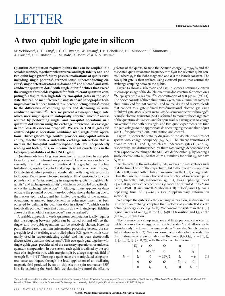
Figure 1a shows a schematic and Fig. 1b shows a scanning electronmicroscope image of the double-quantum-dot structure fabricated on a28Si epilayer with a residual 29Si concentration of 800 p.p.m. (ref. 14).The device consists of three aluminium layers, nine aluminium gates, analuminium lead for ESR control21, and source, drain and reservoir leadsthat connect to a gate-induced two-dimensional electron gas usingmultilevel gate-stack silicon metal–oxide–semiconductor technology22.A single-electron transistor (SET) is formed to monitor the charge stateof the quantum-dot system and for spin read-out using spin-to-chargeconversion23. For both our single- and two-qubit experiments, we tunethe gate voltages to the appropriate dc operating regime and then adjustgate G1 for qubit read-out, initialization and control.
Figure 1c shows the stability diagram of the double-quantum-dotsystem with charge occupancy (N2, N1). The charge transitions ofquantum dots D1 and D2, which are underneath gates G1 and G2,respectively, are distinguished by their gate voltage dependence andtheir capacitive coupling to the SET. We define qubit Q1 by loading asingle electron into D1, so that N1 5 1; similarly for qubit Q2, we haveN2 5 1.
To characterize the individual qubits, we bias the gate voltages suchthat the tunnel time of the respective qubit to the reservoir is approxi-mately 100ms and both qubits are measured in the (1, 1) charge state.Clear Rabi oscillations are observed as a function of microwave pulsetime tp for both qubits, as shown in Fig. 1d. Q1 has a dephasing time ofT�2 ~120 ms, with a coherence time T2 that can be extended up to 28 msusing CPMG (Carr–Purcell–Meiboom–Gill) pulses9, and Q2 has adephasing time of T�2 ~61 ms (see Supplementary Informationsection 3).
We couple the qubits via the exchange interaction, as discussed inref. 2, with an exchange coupling that is electrically controlled via thedetuning energy E (see Fig. 2a, b). We control the system in the (1, 1)region, and read out Q2 at the (1, 1)–(0, 1) transition and Q1 at the(0, 1)–(0, 0) transition.
The presence of a sharp interface and large perpendicular electricfields increases the energy of all excited states24, and allows us toconsider only the lowest five energy states16 (see also SupplementaryInformation section 2). We can consequently describe the system inthe rotating-wave approximation in the basis [Q2, Q1], Y 5 [j", "æ,j", #æ, j#, "æ, j#, #æ, j0, 2æ], with the effective Hamiltonian
H ~
EZ{n V V 0 0
V dEZ=2 0 V t0
V 0 {dEZ=2 V {t0
0 V V {EZzn 0
0 t0 {t0 0 U{E
26666664
37777775ð1Þ
1Centre for Quantum Computation and Communication Technology, School of Electrical Engineering and Telecommunications, The University of New South Wales, Sydney, New South Wales 2052,Australia. 2School of Fundamental Science and Technology, Keio University, 3-14-1 Hiyoshi, Kohoku-ku, Yokohama 223-8522, Japan.
4 1 0 | N A T U R E | V O L 5 2 6 | 1 5 O C T O B E R 2 0 1 5
G2015 Macmillan Publishers Limited. All rights reserved
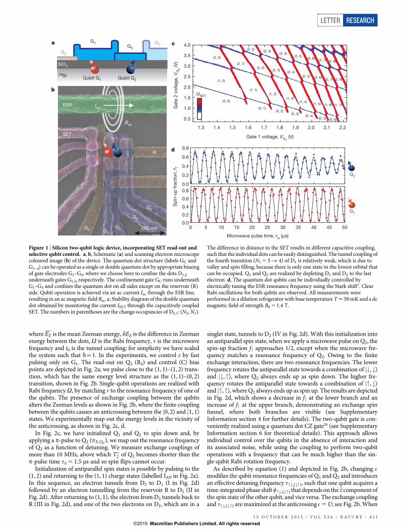
where EZ is the mean Zeeman energy, dEZ is the difference in Zeemanenergy between the dots, V is the Rabi frequency, n is the microwavefrequency and t0 is the tunnel coupling; for simplicity we have scaledthe system such that �h~1. In the experiments, we control e by fastpulsing only on G1. The read-out on Q2 (R2) and control (C) biaspoints are depicted in Fig. 2a; we pulse close to the (1, 1)–(1, 2) trans-ition, which has the same energy level structure as the (1, 1)–(0, 2)transition, shown in Fig. 2b. Single-qubit operations are realized withRabi frequency V, by matching n to the resonance frequency of one ofthe qubits. The presence of exchange coupling between the qubitsalters the Zeeman levels as shown in Fig. 2b, where the finite couplingbetween the qubits causes an anticrossing between the j0, 2æ and j1, 1æstates. We experimentally map out the energy levels in the vicinity ofthe anticrossing, as shown in Fig. 2c, d.
In Fig. 2c, we have initialized Q1 and Q2 to spin down and, byapplying a p-pulse to Q2 (pX,Q2
), we map out the resonance frequencyof Q2 as a function of detuning. We measure exchange couplings ofmore than 10 MHz, above which T�2 of Q2 becomes shorter than thep-pulse time tp 5 1.5 ms and so spin flips cannot occur.
Initialization of antiparallel spin states is possible by pulsing to the(1, 2) and returning to the (1, 1) charge states (labelled IAP in Fig. 2a).In this sequence, an electron tunnels from D2 to D1 (I in Fig. 2d)followed by an electron tunnelling from the reservoir R to D2 (II inFig. 2d). After returning to (1, 1), the electron from D2 tunnels back toR (III in Fig. 2d), and one of the two electrons on D1, which are in a
singlet state, tunnels to D2 (IV in Fig. 2d). With this initialization intoan antiparallel spin state, when we apply a microwave pulse on Q2, thespin-up fraction f" approaches 1/2, except when the microwave fre-quency matches a resonance frequency of Q2. Owing to the finiteexchange interaction, there are two resonance frequencies. The lowerfrequency rotates the antiparallel state towards a combination of j#, #æand j#, "æ, where Q2 always ends up as spin down. The higher fre-quency rotates the antiparallel state towards a combination of j", #æand j", "æ, where Q2 always ends up as spin up. The results are depictedin Fig. 2d, which shows a decrease in f" at the lower branch and anincrease of f" at the upper branch, demonstrating an exchange spinfunnel, where both branches are visible (see SupplementaryInformation section 4 for further details). The two-qubit gate is con-veniently realized using a quantum dot CZ gate20 (see SupplementaryInformation section 6 for theoretical details). This approach allowsindividual control over the qubits in the absence of interaction andits associated noise, while using the coupling to perform two-qubitoperations with a frequency that can be much higher than the sin-gle-qubit Rabi rotation frequency.
As described by equation (1) and depicted in Fig. 2b, changing Emodifies the qubit resonance frequencies of Q1 and Q2 and introducesan effective detuning frequency n"#,(#"), such that one qubit acquires atime-integrated phase shift w"#,(#") that depends on the z component ofthe spin state of the other qubit, and vice versa. The exchange couplingand n"#,(#") are maximized at the anticrossing E5 U; see Fig. 2b. When
1.3 1.4 1.5 1.6 1.7 1.8 1.9 2.0 2.1 2.2
0.5
1.0
1.5
2.0
2.5
3.0
3.5
4.0
Gate
2 v
oltag
e, V
G2 (V
)
Gate 1 voltage, VG1
(V)
a
d
ESR
200 nm
SET
G3
G4
R
b
Q1
Q2
0.0
0.2
0.4
0.6
0.8
Sp
in-u
p f
ractio
n, f ↑
(0, 0)
(1, 1)
(2, 2)
(3, 3)
(1, 0)
(2, 0)
(2, 3)
(1, 2)
(1, 3)
(2, 1)
(1, 4)(1, 5) (1, 6) (1, 7)
(2, 4)
(2, 5) (2, 6)
(3, 4)(3, 5)
(2, 7)
(3, 6)(3, 7)
(0, 1)(0, 2)
(0, 3)(0, 4)
(3, 8)
(3, 2)
(0, 5) (0, 6)B
ac
ΔISET
c
G1
GC
G2
Iac
0 5 10 15 20 25 30 35 40 45 500.0
0.2
0.4
0.6
0.8
Microwave pulse time, τp (μs)
(2, 8)
28Si
SiO2
Qubit Q1
Qubit Q2
GC
G3G
2
G1
Figure 1 | Silicon two-qubit logic device, incorporating SET read-out andselective qubit control. a, b, Schematic (a) and scanning electron microscopecoloured image (b) of the device. The quantum dot structure (labels GC andG1–4) can be operated as a single or double quantum dot by appropriate biasingof gate electrodes G1–G4, where we choose here to confine the dots D1,2
underneath gates G1,2, respectively. The confinement gate GC runs underneathG1–G3 and confines the quantum dot on all sides except on the reservoir (R)side. Qubit operation is achieved via an ac current Iac through the ESR line,resulting in an ac magnetic field Bac. c, Stability diagram of the double quantumdot obtained by monitoring the current ISET through the capacitively coupledSET. The numbers in parentheses are the change occupancies of D2,1: (N2, N1).
The difference in distance to the SET results in different capacitive coupling,such that the individual dots can be easily distinguished. The tunnel coupling ofthe fourth transition (N1 5 3 R 4) of D1 is relatively weak, which is due tovalley and spin filling, because there is only one state in the lowest orbital thatcan be occupied. Q1 and Q2 are realized by depleting D1 and D2 to the lastelectron. d, The quantum dot qubits can be individually controlled byelectrically tuning the ESR resonance frequency using the Stark shift9. ClearRabi oscillations for both qubits are observed. All measurements wereperformed in a dilution refrigerator with base temperature T < 50 mK and a dcmagnetic field of strength B0 5 1.4 T.
1 5 O C T O B E R 2 0 1 5 | V O L 5 2 6 | N A T U R E | 4 1 1
LETTER RESEARCH
G2015 Macmillan Publishers Limited. All rights reserved
a CZ operation is performed such that w"#1 w#"5p, the operationdiffers only by an overall phase from the basis CZ gate25. This overallphase can be removed using single-qubit pulses or via voltage pulsesexploiting the Stark shift9. To realize a CNOT operation using the CZgate, a CZ(p) rotation is performed in between two p/2-pulses on Q2
that have a phase difference w"#.
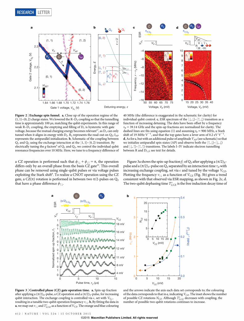
Figure 3a shows the spin-up fraction f" of Q2 after applying a (p/2)X-pulse and a (p/2)Y-pulse on Q2 separated by an interaction time tZ withincreasing exchange coupling, set via E and tuned by the voltage VCZ.Plotting the frequency n"# as a function of VCZ (Fig. 3b) gives a trendconsistent with that observed via ESR mapping, as shown in Fig. 2c, d.The two-qubit dephasing time T�2,CZ is the free induction decay time of
1.64 1.66 1.68 1.70 1.72 1.74 1.76
2.1
2.2
2.3
Gate
2 v
oltag
e, V
G2 (V
)
Gate 1 voltage, VG1
(V)
Q2
b c d
f↑1
0
EZ
Q2 E
Z
Q1
ϵ =
U
VG
1
VP
VP
πX,Q2
VAP
πX,Q2
I
IVR
II
III
f↑1
0
Q1
hν↓↑hν↑↓
(1, 1)
(0, 2)
(0, 1)
(1, 2)
ϵ
ΔISET
a
R2 C
15 20 25 30 35 400
1
2
3
4
5
6
7
8
9
10
Voltage, VP (mV)
50 55 60 65 70 75–16
–14
–12
–10
–8
–6
–4
Fre
qu
en
cy, ν
– ν
0 (M
Hz)
Voltage, VP (mV)
IAP
IAP
R2CR
2C
VP
VAP
|↑, ↑⟩
|0, 2⟩
|↓, ↑ ⟩|↑, ↓⟩E
nerg
y, E
Detuning energy, ϵ
|↓, ↓⟩
ES
R
Figure 2 | Exchange spin funnel. a, Close up of the operation regime of the(1, 1)–(0, 2) charge states. We lowered the R–D2 coupling so that the tunnellingtime is approximately 100 ms, matching the qubit experiments. In this range ofweak R–D1 coupling, the emptying and filling of D1 is hysteretic with gatevoltage, because the mutual charging energy becomes relevant27, as D1 can onlytunnel when it aligns in energy with D2. R2 represents the read-out on Q2; IAP
represents the antiparallel initialization. b, Schematic of the coupling betweenQ1 and Q2 using the exchange interaction at the | 1, 1æ– | 0, 2æ transition. Byelectrically tuning the g factors9 of Q1 and Q2, we control the individual qubitresonance frequencies over 10 MHz. Here, we tune to a frequency difference of
40 MHz (the difference is exaggerated in the schematic for clarity) forindividual qubit control. c, ESR spectrum of the |#, #æ– |", #æ transition as afunction of increasing detuning. The data have been offset by a frequencyn0 5 39.14 GHz and the spin-up fractions are normalized for clarity. Thedashed lines are fits using equation (1) and assuming t0 5 900 MHz, a Starkshift of 19 MHz V21, and that the top gates have a lever arm of 0.2 eV V21.d, As for c, but with an additional pulse of amplitude VAP (see schematic) so thatwe initialize antiparallel spin states (AP) and observe both the |", #æ– |#, #æand |#, "æ– |", "æ transitions. The labels I–IV indicate electron tunnellingbetween R and D1,2; see text for details.
0 5 10 15 200
1
2
3
4
VCZ
(mV)
VCZ
(mV)
0.0
0.1
0.2
0.3
0.4a
ES
R
(π/2)Y,Q2(π/2)X,Q2
VG
1
VP
VCZ
0 5 10 15
Pulse time, τZ (μs)
No
rmaliz
ed
sp
in-u
p f
ractio
n, f ↑
1
0
1
0
1
0
1
0
1
0
1
0
1
0
b
(T*2
,CZ ) –
1 (MH
z)
NC
Z
ν ↑↓
(MH
z)
0 5 10 15 200
5
10
15
20
τZ
R2C
18 mV
16 mV
14 mV
12 mV
11 mV
8 mV
4 mV
VCZ
Figure 3 | Controlled phase (CZ) gate operation time. a, Spin-up fractionafter applying a (p/2)X-pulse, a CZ operation and a (p/2)Y-pulse, for increasingqubit interaction. The exchange coupling is controlled via E, set with VG1 ,resulting in a tunable two-qubit operation frequency n"#. b, By fitting the data ina, we map out n"# and T�2,CZ as a function of VCZ. The orange and blue colouring
and the arrows indicate the axis each data set corresponds to; the colouringof the data corresponds to that in c, indicating VCZ. The inset shows the numberof possible CZ rotations NCZ. Although T�2,CZ decreases with coupling, thenumber of possible two-qubit rotations continues to increase.
4 1 2 | N A T U R E | V O L 5 2 6 | 1 5 O C T O B E R 2 0 1 5
RESEARCH LETTER
G2015 Macmillan Publishers Limited. All rights reserved

the two-qubit system. At large values of detuning (E R ‘) or when theinteraction vanishes (t0 R 0), T�2,CZ reduces to the single-qubit RamseyT�2 . We obtain T�2,CZ by fitting an exponential to the decay of theoscillations in Fig. 3a. These values of T�2,CZ are plotted along withthe measured n"# values in Fig. 3b. We find that the two-qubit dephas-ing rate
�T�2,CZ
�{1rises in step with the exchange coupling and n"#,
which is to be expected because dn:;�dV also increases with n"#,
meaning that the qubit system becomes increasingly sensitive toelectrical noise26. Despite this, the total number of oscillationsNCZ~n:;T�2,CZ also increases with n"#, as shown in Fig. 3b. InSupplementary Information section 7, we show an optimized sequencewhere T�2,CZ~8:3 ms and n"#5 3.14 MHz, such that NCZ . 26.
For all of the experiments described in Figs 2 and 3, we performedread-out only on Q2, owing to its proximity to the reservoir used forspin selective read-out. However, to demonstrate a two-qubit CNOTgate it is desirable to read out the state of both qubits, allowing theobservation of non-classical correlations. This requires a more com-plex pulsing protocol on G1 (Fig. 4a), to first read Q2 at thecharge transition (0, 0)–(0, 1), subsequently read and initialize Q1 at
the (0, 1)–(1, 1) transition, and initialize Q2 at the (0, 0)–(0, 1) trans-ition. The read-out (R1,2) and control (C) bias points are shown on thecharge stability map in Fig. 4b. Following two-qubit read-out of theprevious state, the system is prepared as j#, #æ, after which single-qubitrotations are applied to each qubit to prepare any desired initial two-qubit state.
Figure 4c shows the measured states of Q1 and Q2 after applying theCZ gate as a function of tZ, with Q1 initialized to j"æ (top panel) and j#æ(bottom panel). As expected, the control qubit Q1 (red) is not per-turbed when exchange is turned on because it is in a basis state; how-ever, the target qubit Q2 (blue) is initialized to 1ffiffi
2p j:izj:ið Þ with a
(p/2)X-pulse on Q2 and so rotates about the equator of the Blochsphere when exchange is turned on for time tZ. The strength of theexchange coupling is set so that Q2 rotates about the Bloch sphere atdouble the frequency for Q1 5 j#æ than for Q1 5 j"æ; this is reflected inthe final state of Q2 plotted in Fig. 4c (see Supplementary Informationsection 8 for further details). A CZ gate is realized at tZ 5 480 ns, whenw"#1 w#"5p, and this is converted to a CNOT gate (the target qubit is
0 1 2 3 4 50.0
0.1
0.2
0.3
0.4
0.5
0.60.0
0.1
0.2
0.3
0.4
0.5
0.6
0.0
0.1
0.2
0.3
0.4
0.5
0.6
0 1 2 3 4 50.0
0.1
0.2
0.3
0.4
0.5
0.6
0.0 0.5 1.0 1.5 2.0 2.5 3.00.0
0.4
0.8
Sp
in-u
p f
ractio
n, f ↑
Sp
in-u
p f
ractio
n, f ↑
Interaction time, τZ (μs)
0.0
0.4
0.8
Q1
Q2
Q1
Q2
Tw
o-s
pin
pro
bab
ilities
a
ES
R
CZ
VG
1
τZ
VCZ
ReadQ
2Read/
initialize
Q1
InitializeQ
2
Q2
Q1
Q2
Read/initialization Single- and two-qubit control
1.8 1.9 2.0
2.0
2.1
2.2
2.3
2.4
2.5
VG
2 (V
)
VG1
(V)
R1
R2 C
ΔISETR
1
C
R2 R
2
C
VP
b
(π/2)X (π/2)Xφ↓↑ (τZ)
(π/2)X (π/2)Xφ↑↓ (τZ)
c
CNOT
2π
Q2
Q
1
Q2
Q
1
Q2
Q
1
(1, 1)
(0, 0)
(1, 2)(1, 0)
(0, 1)
VP
VCZ
Q1 microwave pulse time, τ
p (μs)
dπ
CNOTInitialization
τp, Q1
CNOT
Initialization
πX
Figure 4 | Two-spin correlations for a two-qubit logic gate. a, Pulsingprotocol for two-qubit read-out and single- and two-qubit operations. Afterread-out of Q2 (R2) and Q1 (R1), we pulse back to (R2) to ensure properinitialization. Individual qubit operations are performed with high E, whereasthe CZ operation occurs in the presence of interaction. b, Stability diagramshowing the operation regime. c, Spin-up fraction of both qubits afterinitializing Q1 spin up (top) and spin down (bottom) using a microwave pulseand applying a controlled rotation using Q2 as the target qubit. A CNOT gate isachieved in 480 ns, as indicated by the dotted purple line (see inset for the
corresponding Bloch sphere animation). d, Two-spin probabilities as functionsof the microwave pulse length on Q1 after applying a CNOT gate (see inset forthe corresponding Bloch sphere animation), showing clear anticorrelationsbetween the two qubit spin states. The different plots correspond to differentspin states of Q1,2, as indicated. The black lines correspond to fits based on aCNOT gate, and include the experimental read-out errors (see SupplementaryInformation section 9). The green dotted lines correspond to the intendedmaximally entangled states.
1 5 O C T O B E R 2 0 1 5 | V O L 5 2 6 | N A T U R E | 4 1 3
LETTER RESEARCH
G2015 Macmillan Publishers Limited. All rights reserved

flipped when the control qubit is j#æ) by applying (p/2)X-pulses on Q2
before and after the CZ.We use the CNOT gate to create an entangled state of Q1 and Q2. To
realize this, we initialize the qubits first to the j#, #æ state, then apply avarying microwave pulse time to rotate Q1 into superposition states,with a Rabi time tRabi 5 2.4 ms, and finally apply the CNOT gate. Todemonstrate the CNOT gate, we convert the individual qubit spin-upfractions into two-spin probabilities; Fig. 4d shows the four possibletwo-spin probabilities. Clear oscillations are observed in the probabil-ities of the antiparallel states, P(j#, "æ) and P(j", #æ), whereas theseoscillations are almost absent in the probabilities of the parallel states,P(j#, #æ) and P(j", "æ), thereby demonstrating the anticorrelationsexpected for the CNOT gate. The hints of oscillations in the symmetricspin states are probably due to read errors (which are included in thefitted line in Fig. 4d, see also Supplementary Information section 9);our current visibilities are not sufficient to demonstrate violation of theBell inequality.
Future experiments will include improvements to the read-out fide-lities, thus facilitating full two-qubit tomography. The qubit controlfidelities could be further improved by lowering the sensitivity toelectrical noise. Although these silicon qubits represent the smallestscalable two-qubit system reported so far, the complete fabricationprocess is compatible with standard CMOS (complementary metal–oxide–semiconductor) technology, and is also consistent with currenttransistor feature sizes, offering the prospect of realizing a large-scalequantum processor using the same silicon manufacturing technologiesthat have enabled the current information age.
Received 7 November 2014; accepted 22 July 2015.
Published online 5 October 2015.
1. DiVincenzo, D. P. The physical implementation of quantum computation. Fortschr.Phys. 48, 771–783 (2000).
2. Loss, D.& DiVincenzo,D.P.Quantumcomputation withquantumdots. Phys. Rev. A57, 120–126 (1998).
3. Kok, P. et al. Linear optical quantum computing with photonic qubits. Rev. Mod.Phys. 79, 135–174 (2007).
4. Brown, K. R. et al. Single-qubit-gate error below 1024 in a trapped ion. Phys. Rev. A84, 030303 (2011).
5. Barends, R. et al. Superconducting quantum circuits at the surface code thresholdfor fault tolerance. Nature 508, 500–503 (2014).
6. Waldherr, G. et al. Quantum error correction in a solid-state hybrid spin register.Nature 506, 204–207 (2014).
7. Dolde, F. et al. High-fidelity spin entanglement using optimal control. NatureCommun. 5, 3371 (2014).
8. Muhonen, J. T. et al. Storing quantum information for 30 seconds in ananoelectronic device. Nature Nanotechnol. 9, 986–991 (2014).
9. Veldhorst, M. et al. An addressable quantum dot qubit with fault-tolerant fidelity.Nature Nanotechnol. 9, 981–985 (2014).
10. Fowler, A., Marlantoni, M., Martinis, J. M. & Cleland, A. N. Surface codes: towardspractical large-scale quantum computation. Phys. Rev. A 86, 032324 (2012).
11. Shulman, M. D. et al. Demonstration of entanglement of electrostatically coupledsinglet-triplet qubits. Science 336, 202–205 (2012).
12. Nowack, K. C. et al. Single-shot correlations and two-qubit gate of solid-state spins.Science 333, 1269–1272 (2011).
13. Brunner, R. et al. Two-qubit gate of combined single-spin rotation and interdotexchange in a double quantum dot. Phys. Rev. Lett. 107, 146801 (2011).
14. Itoh, K.M. &Watanabe,H. Isotope engineering of siliconanddiamond for quantumcomputing and sensing applications. Mater. Res. Soc. Commun. 4, 143–157(2014).
15. Koppens, F. H. L. et al. Driven coherent oscillations of a single electron spin in aquantum dot. Nature 442, 766–771 (2006).
16. Petta, J. R. et al. Coherent manipulation of coupled electron spins insemiconductor quantum dots. Science 309, 2180–2184 (2005).
17. Medford, J. et al. Self-consistent measurement and state tomography of anexchange-only spin qubit. Nature Nanotechnol. 8, 654–659 (2013).
18. Maune, B. M. et al. Coherent singlet-triplet oscillations in a silicon-based doublequantum dot. Nature 481, 344–347 (2012).
19. Kawakami, E.et al. Electrical control of a long-livedspinqubit in aSi/SiGe quantumdot. Nature Nanotechnol. 9, 666–670 (2014).
20. Meunier, T., Calado, V. E. & Vandersypen, L. M. K. Efficient controlled-phase gate forsingle-spin qubits in quantum dots. Phys. Rev. B 83, 121403(R) (2011).
21. Dehollain, J. P. et al. Nanoscale broadband transmission lines for spin qubitcontrol. Nanotechnology 24, 015202 (2013).
22. Angus, S. J., Ferguson, A. J., Dzurak, A. S. & Clark, R. G. Gate-defined quantum dotsin intrinsic silicon. Nano Lett. 7, 2051–2055 (2007).
23. Elzerman, J. M. et al. Single-shot read-out of an individual electron spin in aquantum dot. Nature 430, 431–435 (2004).
24. Yang, C. H. et al. Spin-valley lifetimes in a silicon quantum dot with tunable valleysplitting. Nature Commun. 4, 2069 (2013).
25. Ghosh, J. et al. High-fidelity controlled-sZ gate for resonator-basedsuperconducting quantum computers. Phys. Rev. A 87, 022309 (2013).
26. Dial, O. E. et al. Charge noise spectroscopy using coherent exchange oscillations ina singlet-triplet qubit. Phys. Rev. Lett. 110, 146804 (2013).
27. Yang, C. H. et al. Charge state hysteresis in semiconductor quantum dots. Appl.Phys. Lett. 105, 183505 (2014).
Supplementary Information is available in the online version of the paper.
Acknowledgements We thank S. Bartlett for discussions and C. M. Cheng forcontributions to the preparation of the experimental setup. We acknowledge supportfrom the Australian Research Council (CE11E0001017), the US Army Research Office(W911NF-13-1-0024) and the NSW Node of the Australian National FabricationFacility. M.V. acknowledges support from the Netherlands Organization for ScientificResearch (NWO) through a Rubicon Grant. The work at Keio was supported in part bythe Grant-in-Aid for Scientific Research by MEXT, in part by NanoQuine, in part byFIRST and in part by the JSPS Core-to-Core Program.
Author Contributions M.V., C.H.Y. and J.C.C.H. performed the experiments. M.V. andF.E.H. fabricated the devices. K.M.I. prepared and supplied the 28Si epilayer wafer. W.H.,J.P.D., J.T.M., S.S andA.L. contributed to the preparationof the experiments. M.V., C.H.Y.,A.M. and A.S.D. designed the experiment and discussed the results. M.V. analysed theresults. M.V. and A.S.D. wrote the manuscript with input from all co-authors.
Author Information Reprints and permissions information is available atwww.nature.com/reprints. The authors declare no competing financial interests.Readers are welcome to comment on the online version of the paper. Correspondenceand requests for materials should be addressed to M.V. ([email protected]) orA.S.D. ([email protected]).
4 1 4 | N A T U R E | V O L 5 2 6 | 1 5 O C T O B E R 2 0 1 5
RESEARCH LETTER
G2015 Macmillan Publishers Limited. All rights reserved