lehrstuhl für technische physik – e d
TRANSCRIPT

Annual ReportJahresbericht 2013
WMI
Walther–Meißner–Institut
für Tieftemperaturforschung
Bayerische Akademie der Wissenschaften

Contact:
Prof. Dr. Rudolf GrossWalther–Meißner–Institut für TieftemperaturforschungBayerische Akademie der WissenschaftenandLehrstuhl für Technische Physik – E23
Technische Universität München
Address:
Walther–Meißner–Str. 8 Phone: +49 – (0)89 289 14201
D - 85748 Garching Fax: +49 – (0)89 289 14206
GERMANY e–mail: [email protected]–address: http://www.wmi.badw.de
Secretary’s Office and Administration:
Emel Dönertas Phone: +49 – (0)89 289 14202
Fax: +49 – (0)89 289 14206
e–mail: [email protected]@wmi.badw.de
Ludwig Ossiander Phone: +49 – (0)89 289 14205
Fax: +49 – (0)89 289 14206
e–mail: [email protected]@wmi.badw.de


Annual Report 2013 1
Preface
Dear colleagues, friends, partners, and alumni of the Walther-Meißner-Institute for Low Tem-perature Research (WMI) of the Bavarian Academy for Sciences and Humanities (BAdW)!
The scientists and students of WMI are pleased to present to you their Annual Report 2013.The report intends to provide you an overview on our last year’s teaching and research activ-ities, ranging from fundamental studies in solid state physics, application oriented research,and materials science to technological developments in low temperature, thin film and nano-technology. Our research interests cover superconductivity and superfluidity, magnetism,ordering and emergent phenomena in correlated electron systems, spin electronics and spincaloritronics, as well as quantum information processing and quantum coherence in solid statesystems. As every year, our Annual Report comes early to give you a timely piece of infor-mation. It is aiming to provide not only concise summaries of our ongoing research projectsand their major results, but also information on our teaching activities as well as statisticaldata about publications, completed and ongoing Ph.D., diploma, master and bachelor theses,collaborations, funding, and recent developments in infrastructure and experimental facilities.
After the busy year 2012 with the evaluation of the Excellence Cluster Nanosystems InitiativeMunich (NIM), a review of the research strategy and performance of the Bavarian Academyfor Sciences and Humanities (BAdW), as well as an midterm review of the EU network Cir-cuit and Cavity Quantum Electro-Dynamics (CCQED), the year 2013 fortunately was lessdemanding regarding review procedures and therefore more productive concerning the sci-entific research performed at WMI. Nevertheless, we have been successful also in 2013 inextending our long-term collaborative research projects. The Transregional Collaborative Re-search Center TRR 80 “From Correlations to Functionality” was granted funding for anotherfour-year period from 2014 until 2017. The same ist true for the Priority Program SPP 1450on “Superconductivity in Iron-Based Compounds”, which was receiving funding for the pe-riod from 2014 to 2016. Moreover, in 2013 a new project entitled Exotic Superconductivityin Strongly Anisotropic Correlated Organic Metals in the Vicinity of Insulating Phases hasbeen granted by the German Research Foundation (DFG), the EU Collaborative Project enti-tled “Quantum Propagating Microwaves in Strongly Coupled Environments – PROMISCE”had a successful midterm review, and finally our application for an International PhD Schoolof Excellence (IDK) entitled “Exploring Quantum Matter (EQM)” within the Elite-NetzwerkBayern was evaluated very positively. We hope that funding for this new graduate school,which we applied for together with Max-Planck Institut für Quantenoptik (MPQ), Ludwig-Maximilians Universität München (LMU) and Technische Universität München (TUM), willstart early in 2014.
Our successful research in 2013 is reflected in more than 30 ISI-listed publications, new ex-tramural funding, and fruitful collaborations with international research institutions and in-dustry. The high international visibility of WMI is documented by more than 1300 citationsof our publications in 2013 and a large number of invited presentations at national and in-ternational conferences. WMI also has organized national and international workshops andconferences, in this way further promoting its scientific visibility. One of the most importantassets of WMI is the large number or talented and dedicated students, working in meanwhilecrowded laboratories and offices. In this year, the total number of student helpers, bachelor,master/diploma and PhD students was exceeding 50 and thus reaching a new all-time recordvalue. In 2013, 19 bachelor, 8 master/diploma and 4 PhD theses were completed, while 14
master/diploma and 18 PhD students are still ongoing with their work. Without any doubt,our successful research would not be possible without the dedicated and hard work of allscientific and technical staff as well as doctorate, diploma/master and bachelor students. Inthe same way, an important prerequisite of success in science is the continuous support by
2013

2 Walther–Meißner–Institut
various funding agencies. In this context we gratefully acknowledge financial support fromthe BAdW, the DFG, the Bavarian Ministry for Science and Arts, the BMBF and the EU. Afurther key to our success in research is the recruitment of outstanding, scientifically indepen-dent group leaders with complementary research interests and technical expertise, a processwhich is supported and monitored by the scientific advisory board of WMI. We are stronglycommitted to support and promote young scientists in their career.
Success in science also has some negative aspects. Carrying out a large number or researchprojects results in a considerable increase of the basic running costs not covered by third-partyfunding. Hence, although we succeeded to keep the third-party funding at a high level ofabout 40% of our full cost budget since several years, the budget situation of WMI is becomingincreasingly difficult and no longer financially viable. This unfortunate development is mainlycaused by the rapid increase of costs for energy. For example, at WMI the costs for electricityincreased by a factor of about four within the last 10 years at an almost constant full costbudget. For 2014, we will have to pay probably 150 kEuro only for the so-called EEG-Umlage.The consequences are missing investments in the technical infrastructure and replacements ofimportant instruments. It is high time that the Bavarian Ministry for Science and Arts takesappropriate measures to keep up the international competitiveness of WMI.
I hope that our Annual Report 2013 inspires your interest in WMI. I take this opportunityto thank all the colleagues, guests, students, post–docs and cooperating partners, who con-tributed to our research and teaching activities within the last year, and last but not least allour friends and sponsors for their interest, trust and continuous support.
Garching, December 2013Rudolf Gross
the majority of the WMI team members
© Walther-Meißner-Institut
Contents
Preface . . . . . . . . . . . . . . . . . . . . . . . . . . . . . . . . . . . . . . . . . . . . . . 1
The Walther–Meißner–Institute . . . . . . . . . . . . . . . . . . . . . . . . . . . . . . . . 5
Scientific Reports: 9
Joint Research Projects 9
The Collaborative Research Center 631 . . . . . . . . . . . . . . . . . . . . . . . . . . . . 11
The Cluster of Excellence “Nanosystems Initiative Munich – NIM” . . . . . . . . . . . 15
The Transregional Collaborative Research Center TRR 80 . . . . . . . . . . . . . . . . . 19
The DFG Priority Program SPP 1285 “Semiconductor Spintronics” . . . . . . . . . . . 20
The DFG Priority Program SPP 1458 “Superconductivity in Iron-Based Compounds” 23
The DFG Priority Program SPP 1538 “Spin Caloric Transport” . . . . . . . . . . . . . . 25
The EU Projects “CCQED” and “PROMISCE” . . . . . . . . . . . . . . . . . . . . . . . 27
Basic Research 31
Time-domain experiments on the quantum switch . . . . . . . . . . . . . . . . . . . . . 33
Switching dynamics of electromechanically induced transparency . . . . . . . . . . . 36
Analysis of the subdominant d wave pairing channel in iron based superconductors . 39
Phase fluctuations, gauge invariance and the Anderson Higgs mechanism in noncentrosymmetric superconductors . . . . . . . . . . . . . . . . . . . . . . . . . . . 41
Phonon anomalies at the helimagnetic phase transition in MnSi . . . . . . . . . . . . . 45
Fermi surface transformation in the electron-doped cuprate superconductor NCCOdetected by high-field Hall effect studies . . . . . . . . . . . . . . . . . . . . . . . 47
Quantum and classical magnetoresistance oscillations in an organic superconductorin the proximity of the Mott transition . . . . . . . . . . . . . . . . . . . . . . . . . 50
Low temperature phase diagram of kappa (BETS)2FeCl4 . . . . . . . . . . . . . . . . . 52
Spin pumping in the strong coupling regime . . . . . . . . . . . . . . . . . . . . . . . . 54
Spin Hall magnetoresistance . . . . . . . . . . . . . . . . . . . . . . . . . . . . . . . . . . 57
Magnon, phonon and electron temperature profiles and the spin Seebeck effect inmagnetic insulator/normal metal hybrid structures . . . . . . . . . . . . . . . . . 60
3

4 Walther–Meißner–Institut
Application–Oriented Research 63
Superconducting microwave resonators with tunable coupling . . . . . . . . . . . . . . 65
Squeezed coherent states with flux-driven Josephson parametric amplifier . . . . . . . 67
Noise properties of a flux-driven Josephson parametric amplifier in the degeneratemode . . . . . . . . . . . . . . . . . . . . . . . . . . . . . . . . . . . . . . . . . . . . 69
Materials, Thin Film and Nanotechnology, Experimental Techniques 71
Pyrochlore iridates: candidates for the realization of Weyl nodes . . . . . . . . . . . . 73
Progress in the WMI Quantum Laboratory . . . . . . . . . . . . . . . . . . . . . . . . . 75
Cryogen free dilution fridge with large sample stage . . . . . . . . . . . . . . . . . . . 77
Vibrations in a dry fridge: Surprise, surprise! . . . . . . . . . . . . . . . . . . . . . . . . 79
Experimental Facilities 81
Overview of Key Experimental Facilities and Infrastructure . . . . . . . . . . . . . . . 83
Publications 97
Books 101
Bachelor, Master, and PhD Theses 103
Research Projects, Workshops, Collaborations, Stays abroad etc. 109
Invited Conference Talks and Seminar Lectures 117
Appointments, Honors and Awards, Membership in Advisory Boards, etc. 123
Seminars, Courses, Lectures and other Scientific Activities 125
Staff of the Walther-Meißner-Institute 137
Guest Researchers 139
Commission for Low Temperature Physics 141
© Walther-Meißner-Institut
Annual Report 2013 5
The Walther–Meißner–Institute
General Information
The Walther–Meißner–Institute for Low Temperature Research (WMI) is operated by the Com-mission for Low Temperature Research of the Bavarian Academy of Sciences and Humanities(BAdW). The commission was founded in 1946 on Walther Meißner’s initiative, who waspresident of BAdW from 1946 to 1950. The Commissions (Research Groups) of the Academyare set up in order to carry out long–term projects, which are too ambitious for the lifetimeor capacity of any single researcher, or which require the collaboration of specialists in vari-ous disciplines. At present, the Bavarian Academy of Sciences and Humanities consists of 36
Commissions with more than 300 employees.
The Commission for Low Temperature Research of the BAdW started its research activitiesin 1946 in the Herrsching barracks. After the retirement of Walther Meißner in 1952, HeinzMaier-Leibnitz, who followed Walther Meißner on the Chair for Technical Physics of the Tech-nische Universität München, became the new head of the Commission for Low TemperatureResearch. In 1967, the commission moved to the Garching research campus after the construc-tion of the new "Zentralinstitut für Tieftemperaturforschung" (ZTTF) was completed (director:Prof. Heinz Maier-Leibnitz, technical director: Prof. Franz Xaver Eder). Until 1972, the theorygroup of the Institute Laue Langevin was hosted at the ZTTF. In 1980, Prof. Dr. Klaus Andresbecame the new director of the ZTTF again associated with the Chair for Technical Physics(E23) at the Technische Universität München, followed by Prof. Dr. Rudolf Gross in 2000. In1982, the ZTTF was renamed into Walther-Meißner-Institute for Low Temperature Research(WMI) on the occasion of Walther Meißner’s 100. birthday.
As already mentioned, it is a long tradition that WMI hosts the Chair for Technical Physics(E 23) of the Technische Universität München (TUM) with the director of the WMI beinga full professor at the Faculty of Physics of TUM. However, there are also close ties withthe Ludwig-Maximilians-Universität (LMU). Between 2004 and 2010, WMI hosted a scanningprobe division with the head of this division being a professor at the Ludwig-Maximilians-Universität (LMU). In this way a tight collaboration has been established between WMI andresearch groups of both Munich universities, joining technological and human resources inthe fields of experimental and theoretical solid-state and condensed matter physics, low tem-perature techniques, materials science as well as thin film and nanotechnology. Noteworthy,the WMI supplies liquid helium to more than 25 research groups at both Munich universitiesand provides the technological basis for low temperature research.
Research Activities
The research activities of the Walther–Meißner–Institute are focused on low temperature solid-state and condensed matter physics (see reports below). The research program is devoted toboth fundamental and applied research and also addresses materials science, thin film andnanotechnology aspects. With respect to basic research the main focus of the WMI is on
• superconductivity and superfluidity,• magnetism, spin transport, spin mechanics and spin caloritronics,• quantum phenomena and quantum coherence in mesoscopic systems and nanostruc-
tures,• circuit-quantum electrodynamics and circuit-nanomechanics,• ordering and emergent phenomena in correlated electron systems,• and the general properties of metallic systems at low and very low temperatures.
2013

6 Walther–Meißner–Institut
The WMI also conducts applied research in the fields of
• solid-state quantum information processing systems,• superconducting and spintronic devices,• oxide electronics,• multi-functional and multiferroic materials,• and the development of low and ultra low temperature systems and techniques.
With respect to materials science, thin film and nanotechnology the research program isfocused on
• the synthesis of superconducting and magnetic materials,• the single crystal growth of oxide materials,• the thin film technology of complex oxide heterostructures including multifunctional
and multiferroic material systems,• and the fabrication of superconducting, magnetic, and hybrid nanostructures.
The WMI also develops and operates systems and techniques for low and ultra–low tempera-ture experiments. A successful development have been dry mK-systems that can be operatedwithout liquid helium by using a pulse-tube refrigerator for precooling. Meanwhile, these sys-tems have been successfully commercialized by the company VeriCold Technologies GmbHat Ismaning, Germany, which was taken over by Oxford Instruments in 2007. As furthertypical examples we mention a nuclear demagnetization cryostat for temperature down tobelow 100 µK, or very flexible dilution refrigerator inserts for temperatures down to about20 mK mK fitting into a 2 inch bore. These systems have been engineered and fabricated at theWMI. Within the last years, several dilution refrigerators have been provided to other researchgroups for various low temperature experiments. The WMI also operates a helium liquifierwith an annual capacity of well above 150.000 liters and supplies both Munich universitieswith liquid helium. To optimize the transfer of liquid helium into transport containers theWMI has developed a pumping system for liquid helium that is commercialized in collabora-tion with a company.
To a large extent the research activities of WMI are integrated into national and internationalresearch projects such as Clusters of Excellence, Collaborative Research Centers, ResearchUnits, or EU projects. The individual research groups of WMI offer a wide range of attrac-tive research opportunities for diploma (graduate) students, PhD students and postdoctoralfellows.
Experimental Facilities and Resources
The WMI is equipped with state of the art facilities for the preparation and characterization ofsuperconducting and magnetic materials as well as for various low and ultra–low temperatureexperiments. The main experimental and technological resources of WMI are listed in thefollowing.
Materials Preparation and Fabrication of Nanostructures
• Laser Molecular Beam Epitaxy (L-MBE) system for oxide heterostructures (equippedwith in–situ RHEED, Omicron AFM/STM system, atomic oxygen/nitrogen source,infrared-laser heating system, metallization)
• molecular beam epitaxy (MBE) system for metallic systems• UHV magnetron sputtering systems for metals (e.g. Nb, Al, NiPd, ... )
© Walther-Meißner-Institut

Annual Report 2013 7
• magnetron sputtering system for oxide heteroepitaxy (equipped with four sputteringguns and an oxygen ion gun)
• reactive ion etching (RIE) system, Plasmalab 80 Plus with ICP plasma source, OxfordInstruments Plasma Technology
• ion beam etching (IBE) system equipped with a LN2 cooled sample holder• polishing machine for substrate preparation• ultrasonic bonding machine• 50 m2 class 1000 clean room facility• optical lithography (Süss maskaligner MJB 3 and projection lithography)• electron beam lithography (based on Philips XL 30 SFEG scanning electron microscope
and Raith Elphy Plus lithography system including a laser stage)• four-mirror image furnace for crystal growth
Characterization
• 2–circle x–ray diffractometer (Bruker D8 Advance, sample temperature up to 1 600C)
• high resolution 4–circle x–ray diffractometer with Göbel mirror and Ge monochromator(Bruker D8 Discover)
• scanning electron microscope with EDX analysis• UHV room temperature AFM/STM system• 2048 u high resolution mass spectrometer (Fa. Pfeiffer, cross-beam ion source, SEM)• Low Energy Electron Diffraction (SPECTA-LEED, Fa. Omicron)• two Raman spectroscopy systems (1.5 to 300 K, in-situ sample preparation)• SQUID magnetometer (Quantum Design, 1.5 to 700 K, up to 7 T)• several high field magnet systems (up to 17 T Tesla) with variable temperature inserts• 7 T split coil magnet systems with optical access and variable temperature insert• 3D vector magnet (2/2/6 Tesla) with variable temperature inserts• experimental set–ups for the measurement of noise including low noise SQUID ampli-
fiers and signal analyzers• high-frequency network analyzers (up to 40 GHz) and various microwave components
(sources, mixers, circulators, attenuators) for the determination of high frequency pa-rameters
• ultra-sensitive microwave receiver for state tomography of quantum microwaves (dualpath method with FPGA signal processing)
• high-frequency cryogenic probing station (up to 20 GHz, T > 4 K)• magnetooptical Kerr effect (MOKE) system• ferromagnetic resonance (FMR) system
Low temperature systems and techniques
• 5 K-Scanning Tunneling Microscope (low temperature STM, Fa. Omicron)• several 3He/4He dilution refrigerator inserts for temperatures down to 10 mK• “dry” mK-cooler based on a dilution refrigerator with pulse-tube precooling• “dry” dilution refrigerator with a base temperature of about 10 mK equipped with a 3D
vector magnet (1/1/6 Tesla)• ultra–low temperature facility for temperatures down to below 100 µK based on a nu-
clear demagnetization cryostat• experimental set–ups for the measurement of specific heat, magnetization, thermal ex-
pansion as well as electrical and thermal transport properties as a function of tempera-ture, magnetic field and pressure
2013

8 Walther–Meißner–Institut
© Walther-Meißner-Institut

Joint Research Projects
TRR 80
SPP 1285 SPP 1458 SPP 1538
9


Annual Report 2013 11
The Collaborative Research Center 631
F. Deppe, R. Gross, H. Hübl, A. Marx1
The Collaborative Research Center 631 (SFB 631) on Solid State Quantum Information Pro-cessing was established in 2003 and extended for a second and a third four-year funding in2007 and 2011, respectively. The third funding period will last until June, 2015.
Since the start of SFB 631 a decade ago, quantum informationscience has developed into a fascinating and one of the mostrapidly growing fields of science and technology. It residesat the interface between physics, mathematics, computer andmaterials science, and engineering. It is concerned with bothfundamental questions and technological developments, aim-ing at the realization of a useful quantum information hard-ware.
At WMI, the study of the physics of solid state quantum sys-tems has developed into a key research field. Besides super-conducting quantum circuits, the research activities of WMI meanwhile include also quantumspin systems and mechanical systems, as well as systems combining different degrees of free-dom in quantum hybrid structures. Our research within SFB 631 does not only provide thefoundations of quantum information systems and quantum technology, but also addresseskey fundamental questions regarding quantum coherence, quantum dynamics and decoher-ence processes in solid state quantum systems. Furthermore, it requires extremely sensitivemeasurements at low and ultra-low temperatures and therefore perfectly fits to the researchprofile of WMI.
The research effort of SFB 631 is highly collaborative and interdisciplinary. To cover the broadspectrum of fundamental and application oriented questions related to solid state quantuminformation systems in a comprehensive way, SFB 631 joins research activities from quan-tum information theory, experimental and theoretical solid state physics, quantum optics,materials science, and nanotechnology. Today, within SFB 631 research groups from theBavarian Academy of Sciences and Humanities (BAdW), the TU Munich (TUM), the Ludwig-Maximilians-University (LMU), the Max-Planck-Institute for Quantum Optics (MPQ), as wellas Augsburg and Regensburg University are collaborating in 17 research projects. At present,SFB 631 joins more than 30 principal investigators and more than 60 Ph.D. and diploma stu-dents, as well as a large number of postdocs and guest scientists. WMI is one of the mainactors, not only being involved in the three projects A3 (Gross, Hübl, Marx), A8 (Gross, Marx,Deppe) and C3 (Hübl), but also providing the coordination of the center from the beginning(spokesman: Rudolf Gross).
Within the project A3 on Superconducting Quantum Circuits as Basic Elements for Quantum In-formation Processing and project A8 on Cavity Quantum Electrodynamics with SuperconductingDevices, the research program of WMI within SFB 631 is focusing on the fabrication andstudy of superconducting quantum information circuits. This includes the fabrication of su-perconducting flux qubits in which quantum mechanical superposition states of clockwiseand counter-clockwise circulating persistent currents are used for the realization of solid statequbits. A particular development of WMI is the realization of flux qubits with tunable gapwhich offer more flexibility in circuit design [1]. These qubits are coupled to superconduct-ing microwave resonators. In this way fascinating quantum electrodynamic experiments withdeliberately designed artificial solid state atoms become possible. Since such experiments are
1This work is supported by the German Research Foundation through SFB 631.
2013

12 Walther–Meißner–Institut
completely analogous to quantum optical experiments on natural atoms in optical resonators,this prospering new field is called circuit quantum electrodynamics (circuit QED). Here, par-ticular goals are the strong and ultra-strong coupling [2] of superconducting qubits to high-quality superconducting microwave resonators, the generation and detection of non-classicalmicrowave states (e.g. Fock or squeezed states), the development of dispersive readout andquantum non-demolition measurements, and the entanglement of superconducting qubits viamultiple resonators. Regarding these research goals the WMI team closely collaborates withthe theory groups at LMU (von Delft), the University of Augsburg (Hänggi), the Universidaddel País Vasco - Euskal Herriko Unibertsitatea at Bilbao (Solano), and the Instituto de FísicaFundamental at Madrid (Garcia-Ripoll), as well as the experimental groups at the NTT Ba-sic Research Laboratories (Semba) and the Nano Electronics Research Laboratories at NECCorporation, Japan (Nakamura, Tsai, Yamamoto). The research work within SFB 631 is alsoclosely linked to the activities within Research Area I of the Cluster of Excellence NanosystemsInitiative Munich (NIM) (see pp. 15–18).
Figure 1: Top: Optical micrograph showing the circuit design of asuperconducting quantum switch. Bottom: Parts of the couplingregion marked in the upper subfigure by the red rectangle shownon an enlarged scale. The green structures represent the inner con-ductors of the two coplanar waveguide resonators, the red ones thegalvanically coupled qubit loop with the three Al/AlOx/Al Joseph-son junctions.
Analogous to the field of cav-ity quantum electrodynamics (cav-ity QED), in circuit QED the inter-action between light and matter isstudied. In 2013, we could realizea central element of superconduct-ing circuit QED, a so-called quan-tum switch [3, 4] providing tunableand switchable coupling betweentwo superconducting resonators viaa superconducting flux quantum bit(see report by A. Baust et al., pp. 33–35). The coupling of the two res-onators via a single flux qubit al-lows for the realization of a tun-able coupling which depends on thequbit state. Most importantly, thetwo resonators can be completelydecoupled by setting the magneticflux through the qubit such thatthe dynamical coupling just com-pensates for the geometric coupling,yielding effective zero coupling be-tween the two resonators. Thequantum switch circuit also can beused to create entangled quantum
states. We successfully implemented a quantum switch consisting of two superconductingcoplanar stripline resonators and a flux qubit, all fabricated on the same chip. Spectroscopymeasurements demonstrated the switching between the coupled and the decoupled state. Thesetup allowed us to achieve an on-off ratio sufficient for many applications in quantum in-formation systems. As shown in the report by A. Baust et al. (see pp. 33–35), we also couldperform time domain experiments on the quantum switch, making the switchable coupling di-rectly observable. In this way we could provide direct experimental evidence for the expectedswitching behavior, as the transfer of energy from one into another resonator controlled bythe qubit state could be directly observed.
In circuit QED architectures with multiple qubits and resonators, meanwhile quantum logicgates have been successfully realized [5, 6]. However, while the requirements for such digital
© Walther-Meißner-Institut

Annual Report 2013 13
quantum computing circuits are still enormous, analog quantum simulation with circuit QEDsystems appears to be a technologically less demanding, and therefore interesting goal. Inanalog quantum simulations, one mimics the Hamiltonian of a system of interest with a circuitoffering a higher degree of controllability than the original system. In this context, one specificproposal is to strongly couple nonlinear resonators to explore Bose-Hubbard physics in thedriven-dissipative regime [7, 8]. For such experiments, a scalable approach to tunable couplingbetween the resonators is strongly desirable. As shown by the report of Wulschner et al. (seepp. 65–66), we achieved promising experimental progress in this direction. We successfullyfabricated two LC microwave resonators coupled via an RF SQUID [9], representing basicbuilding blocks of superconducting quantum simulators.
Figure 2: Reconstructed Wigner functions (color map) of squeezed vac-uum and squeezed thermal states incident at the input port of the mi-crowave beam splitter. p and q are dimensionless quadrature variablesspanning the phase space. The insets show the 1/e-contours of the idealvacuum (blue), the experimental vacuum or thermal states (green), andthe squeezed vacuum or squeezed thermal states (red). (a) Constant30 dB-attenuator temperature of 50 mK. (b) Constant signal gain of 1 dB.Reprinted from Ref. [10].
After having demonstrated forthe first time path entangle-ment of propagating quantummicrowaves using superconduct-ing circuits and quantum signalrecovery techniques [11–13], wesuccessfully realized squeezedcoherent states with a flux-drivenJosephson parametric amplifier(see Ref. [10] and report by L.Zhong et al., pp. 67–68). Joseph-son parametric amplifiers (JPAs)are promising devices to achievelow-noise amplification. In thenon-degenerate mode, JPAs be-have like linear amplifiers withnoise temperature approachingthe standard quantum limit dic-tated by the Heisenberg uncer-tainty relation. In the degener-ate mode, JPAs are phase sen-sitive amplifiers which can am-plify a signal quadrature witha noise temperature below thestandard quantum limit of lin-ear amplifiers, and at the sametime squeeze another quadraturebelow the vacuum fluctuations.In this way, JPAs allowed us tostudy the squeezing physics ofpropagating quantum microwaves. We used the dual-path state reconstruction method devel-oped at WMI [11–13] and applied it to the study of squeezed coherent states generated by aflux-driven JPA [10]. Moreover, we successfully analyzed the noise properties of a flux-drivenparametric amplifier with the WMI dual-path state reconstruction method (see Refs. [12–14]and report by L. Zhong et al., pp. 69–70)
In a fruitful collaboration with the Finley group at Walter Schottky Institute, we depositedNbN thin films by DC magnetron sputtering on [100] GaAs substrates, optimized their quality,and demonstrated their use for efficient single photon detection in the near-infrared [15].Meanwhile the superconducting single photon detectors (SSPDs) have been successfully usedfor the efficient on-chip time resolved detection of quantum dot emission. The quantum lightemitted by the self-assembled InGaAs quantum dots (QDs) was routed into the optical modes
2013

14 Walther–Meißner–Institut
Figure 3: (a) Self assembled InGaAs quantum dots embed-ded in a GaAs ridge waveguide are excited using a heliumneon laser. The light emitted by the quantum dots is detectedeither in a confocal geometry or guided along the waveguideand evanescently coupled into a NbN SSPD. (b) Layer struc-ture of the sample as prepared by molecular beam epitaxyand reactive magnetron sputtering. Reprinted from Ref. [16].
of a GaAs ridge waveguide and detectedon-chip via evanescent coupling to theNbN SSPD [16].
We also considerably extended the experi-mental facilities for ultra low-noise exper-iments on superconducting quantum cir-cuits. As shown in the report by J. Goetzet al. (see pp. 75–76) the new dilutionrefrigerator in the Quantum LaboratoryK04 has been improved regarding cool-ing power. Furthermore, a new liquid he-lium dewar and measurement equipmenthas been installed, allowing now for de-manding experiments on superconduct-ing quantum circuits. The setting up ofa new cryogen-free dilution refrigeratorwith a pulse tube refrigerator (PTR) pre-
cooling and a large sample stage in the Quantum Laboratory K21 is approaching completion.All components for the 1 K-stage and for the dilution circuit have been fabricated in the WMIworkshop and the wiring for thermometry down to the mixing chamber plate has been in-stalled (see report by A. Marx et al., pp. 77–78).
References
[1] M. J. Schwarz, J. Goetz, Z. Jiang, T. Niemczyk, F. Deppe, A. Marx, and R. Gross. Gradiometric flux qubitswith tunable gap. arXiv:1210.3982 (2012).
[2] T. Niemczyk, F. Deppe, H. Huebl, E. P. Menzel, F. Hocke, M. J. Schwarz, J. J. Garcia-Ripoll, D. Zueco, T.Hummer, E. Solano, A. Marx, and R. Gross, Nat Phys 6, 772–776 (2010).
[3] E. Hoffmann. Experiments on Two-Resonator Circuit Quantum Electrodynamics: A Superconducting QuantumSwitch. Ph.D. thesis, TU München (2013).
[4] M. Mariantoni, F. Deppe, A. Marx, R. Gross, F. Wilhelm, and E. Solano, Phys. Rev. B 78, 104508 (2008).[5] E. Lucero, R. Barends, Y. Chen, J. Kelly, M. Mariantoni, A. Megrant, P. O. Malley, D. Sank, A. Vainsencher, J.
Wenner, T. White, Y. Yin, A. N. Cleland, and J. M. Martinis, Nature Phys. 8, 719–723 (2012).[6] A. Fedorov, L. Steffen, M. Baur, M. P. da Silva, and A. Wallraff, Nature 481, 170–172 (2011).[7] M. Leib, and M. J. Hartmann, New J. of Phys. 12, 093031 (2010).[8] M. Leib, F. Deppe, A. Marx, R. Gross, and M. J. Hartmann, New Journal of Physics 14, 075024 (2012).[9] B. Peropadre, D. Zueco, F. Wulschner, F. Deppe, A. Marx, R. Gross, and J. Garcia-Ripoll, Phys. Rev. B 87,
134504 (2013).[10] L. Zhong, E. P. Menzel, R. D. Candia, P. Eder, M. Ihmig, A. Baust, M. Haeberlein, E. Hoffmann, K. Inomata,
T. Yamamoto, Y. Nakamura, E. Solano, F. Deppe, A. Marx, and R. Gross, New Journal of Physics 15, 125013
(2013).[11] E. P. Menzel, R. Di Candia, F. Deppe, P. Eder, L. Zhong, M. Ihmig, M. Haeberlein, A. Baust, E. Hoffmann,
D. Ballester, K. Inomata, T. Yamamoto, Y. Nakamura, E. Solano, A. Marx, and R. Gross, Phys. Rev. Lett. 109,250502 (2012).
[12] E. P. Menzel, F. Deppe, M. Mariantoni, M. A. Araque Caballero, A. Baust, T. Niemczyk, E. Hoffmann, A.Marx, E. Solano, and R. Gross, Phys. Rev. Lett. 105, 100401 (2010).
[13] E. P. Menzel. Propagating Quantum Microwaves: Dual-path State Reconstruction and Path Entanglement. Disser-tation, Technische Universität München (2013).
[14] R. Di Candia, E. P. Menzel, L. Zhong, F. Deppe, A. Marx, R. Gross, and E. Solano. Dual-Path Methods forPropagating Quantum Microwaves. Accepted for publication in New J. of Phys., arXiv:1308.3117 (2013).
[15] G. Reithmaier, J. Senf, S. Lichtmannecker, T. Reichert, F. Flassig, A. Voss, R. Gross, and J. J. Finley, Journal ofApplied Physics 113, 143507 (2013).
[16] G. Reithmaier, S. Lichtmannecker, T. Reichert, P. Hasch, K. Mueller, M. Bichler, R. Gross, and J. J. Finley,Scientific Reports 3, – (2013).
© Walther-Meißner-Institut

Annual Report 2013 15
The Cluster of Excellence “Nanosystems Initiative Munich – NIM”
F. Deppe, S.T.B. Gönnenwein, R. Gross, H. Hübl, A. Marx1
The excellence cluster Nanosystems Initiative Munich (NIM) com-prises internationally recognized expertises in all relevant researchareas of nanosciences, ranging from quantum nanophysics to thecreation and study of nanosystems for biophysics and the life sci-ences. NIM’s overall scientific vision is to integrate nanometer sizedbuilding blocks as well as bio-molecular assemblies into entire func-tional systems.
NIM was launched in 2006. The first six-year fundingperiod of NIM ended in October 2012. After an inter-mediate evaluation, NIM was granted a further five-year funding period until end of 2017. NIM joins re-search groups from LMU Munich, TU Munich, WMI,the University of Augsburg, the Munich Universityof Applied Science, the Max-Planck-Institutes for Bio-chemistry and Quantum Optics, and the DeutschesMuseum. NIM’s future research activities are orga-nized in five research areas (RAs) as shown in thefigure: RA I – Quantum Nanophysics, RA II – Hy-brid Nanosystems, RA III – Nanosystems for En-ergy Conversion, RA IV – Biomolecular Nanosys-tems, and RA V – Biomedical Nanotechnologies. AtWMI, several scientists (Deppe, Gönnenwein, Gross,Hübl, Marx) actively contribute to the ambitious re-search program of the second funding period of NIM.
The physics of quantum nanosystems is one of the main future research directions of NIM,in perfect agreement with the focus of several research activities at WMI. The major contribu-tions of WMI are to RA I: Quantum Nanophysics and RA II: Hybrid Nanosystems. Researcharea I is coordinated by R. Gross of WMI.
Area I: Quantum Nanophysics
... providing the foundations of quantum nanosystems
The scientific program of Research Area I is fo-cused on quantum nanosystems. It aims at themodeling and understanding of such nanosys-tems on a quantum level. The modelling andunderstanding of nanosystems on a quantumlevel is a key prerequisite for their applicationin hybrid devices, energy conversion systemsas well as in biomolecular and biomedical sys-tems. The scientific program of research areaI addresses this fundamental problem by sys-tematically studying quantum systems basedon solid state nanostructures and tailor-mademeso-scale many body systems realized in optical lattices.
A particular objective of the WMI activities within RA I is the systematic study of the interac-tion between nanoscale solid state quantum systems and the modes of electromagnetic fieldson a single quantum level. To this end, we could realize strong coupling between the magnetic
1This work is supported by the German Excellence Initiative via the Nanosystems Initiative Munich (NIM).
2013
16 Walther–Meißner–Institut
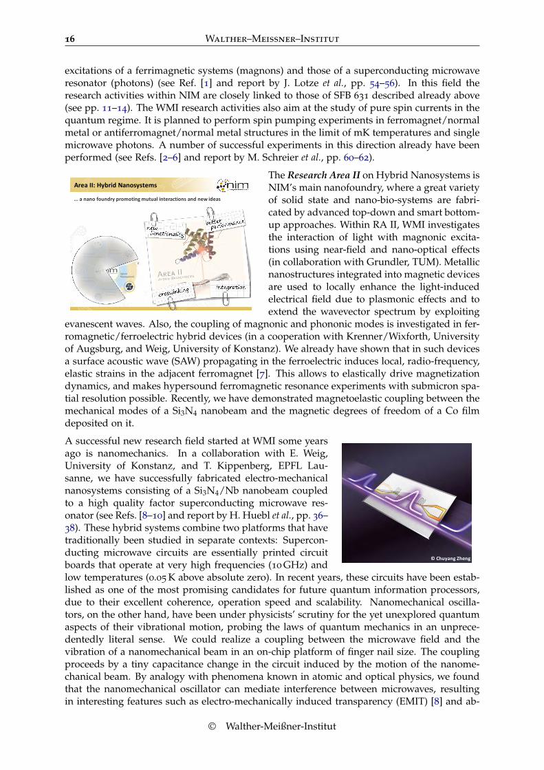
excitations of a ferrimagnetic systems (magnons) and those of a superconducting microwaveresonator (photons) (see Ref. [1] and report by J. Lotze et al., pp. 54–56). In this field theresearch activities within NIM are closely linked to those of SFB 631 described already above(see pp. 11–14). The WMI research activities also aim at the study of pure spin currents in thequantum regime. It is planned to perform spin pumping experiments in ferromagnet/normalmetal or antiferromagnet/normal metal structures in the limit of mK temperatures and singlemicrowave photons. A number of successful experiments in this direction already have beenperformed (see Refs. [2–6] and report by M. Schreier et al., pp. 60–62).
Area II: Hybrid Nanosystems
... a nano foundry promoting mutual interactions and new ideas
The Research Area II on Hybrid Nanosystems isNIM’s main nanofoundry, where a great varietyof solid state and nano-bio-systems are fabri-cated by advanced top-down and smart bottom-up approaches. Within RA II, WMI investigatesthe interaction of light with magnonic excita-tions using near-field and nano-optical effects(in collaboration with Grundler, TUM). Metallicnanostructures integrated into magnetic devicesare used to locally enhance the light-inducedelectrical field due to plasmonic effects and toextend the wavevector spectrum by exploiting
evanescent waves. Also, the coupling of magnonic and phononic modes is investigated in fer-romagnetic/ferroelectric hybrid devices (in a cooperation with Krenner/Wixforth, Universityof Augsburg, and Weig, University of Konstanz). We already have shown that in such devicesa surface acoustic wave (SAW) propagating in the ferroelectric induces local, radio-frequency,elastic strains in the adjacent ferromagnet [7]. This allows to elastically drive magnetizationdynamics, and makes hypersound ferromagnetic resonance experiments with submicron spa-tial resolution possible. Recently, we have demonstrated magnetoelastic coupling between themechanical modes of a Si3N4 nanobeam and the magnetic degrees of freedom of a Co filmdeposited on it.
© Chuyang Zheng
A successful new research field started at WMI some yearsago is nanomechanics. In a collaboration with E. Weig,University of Konstanz, and T. Kippenberg, EPFL Lau-sanne, we have successfully fabricated electro-mechanicalnanosystems consisting of a Si3N4/Nb nanobeam coupledto a high quality factor superconducting microwave res-onator (see Refs. [8–10] and report by H. Huebl et al., pp. 36–38). These hybrid systems combine two platforms that havetraditionally been studied in separate contexts: Supercon-ducting microwave circuits are essentially printed circuitboards that operate at very high frequencies (10 GHz) andlow temperatures (0.05 K above absolute zero). In recent years, these circuits have been estab-lished as one of the most promising candidates for future quantum information processors,due to their excellent coherence, operation speed and scalability. Nanomechanical oscilla-tors, on the other hand, have been under physicists’ scrutiny for the yet unexplored quantumaspects of their vibrational motion, probing the laws of quantum mechanics in an unprece-dentedly literal sense. We could realize a coupling between the microwave field and thevibration of a nanomechanical beam in an on-chip platform of finger nail size. The couplingproceeds by a tiny capacitance change in the circuit induced by the motion of the nanome-chanical beam. By analogy with phenomena known in atomic and optical physics, we foundthat the nanomechanical oscillator can mediate interference between microwaves, resultingin interesting features such as electro-mechanically induced transparency (EMIT) [8] and ab-
© Walther-Meißner-Institut

Annual Report 2013 17
sorption (EMIA) [9, 10], and can be exploited to control the propagation of microwave signals.In particular, we could create spectrally extremely sharp transmission windows (linewidth10 Hz) for microwave radiation, which are accompanied by very long delays on the order of10 milliseconds [8–10]. We also addressed more subtle questions with regard to the possi-ble temporal dynamics of the control that have been debated among experts, and found fullagreement with their expectations [8, 10]. Another important result was that our system iscapable of operating in a regime in which decoherence, a potentially detrimental effect for theprocessing of quantum information, is not a critical issue. In summary, we developed a plat-form to manipulate wave propagation in a fully integrated architecture without the need ofphoton detection and regeneration. Its implications extend to the field of quantum computingand quantum information processing.
Exploiting New Media and
Getting Trained in Science 2.0
in an ENB PhD School Setting up an
E-Library of Excellence
in Exchange with International Doctoral Training Centres and
Partners at the Austrian Academy of Sciences in Vienna and Innsbruck, at
ETH-Zurich, ICFO in Barcelona, Imperial College London, Caltech,
and Harvard University etc.
Exploring Quantum Matter (EQM) Application for an International PhD School of Excellence (IDK) within Elite-Netzwerk Bayern
Full Proposal
Max-Planck Institut für Quantenoptik (MPQ) Bayerische Akademie der Wissenschaften Walter-Schottky Institut Zentrum für Nanotechnologie & Nanomaterialien Ludwig-Maximilians Universität München (LMU) Technische Universität München (TUM)
In order to unite the unique competences inquantum physics in Munich and extend theminto an international excellence network of doc-toral training centres with partners at the Aus-trian Academy of Science in Vienna and Inns-bruck, at ETH Zurich, ICFO Barcelona, Im-perial College London, Caltech, and Harvard,we applied for an International PhD Schoolof Excellence (IDK) entitled “Exploring Quan-tum Matter (EQM)” within Elite-Netzwerk Bay-ern in 2013. The proposal has been evaluatedvery positively and the final decision on fund-ing will be made in January 2014. The partic-ipating institutions are Max-Planck Institut fürQuantenoptik (MPQ), Walther-Meißner-Institutof BAdW, Walter-Schottky Institut, Ludwig-Maximilians Universität München (LMU), andTechnische Universität München (TUM). Ex-ploring Quantum Matter from few-body inter-actions to artificial many-body systems will pro-vide a common research focus to unite the com-
petences of leading research groups in Munich in an interdisciplinary, professional and uni-fied manner: quantum many-body systems will be studied in experimental and theoreticalphysics, material science, mathematics, computer science, and chemistry.
The particular focus of WMI within the applied International PhD School of Excellence willbe “Scalable networks of solid-state quantum circuits”, which are becoming increasinglyattractive for quantum simulations. For example, networks of nonlinear superconductingtransmission line resonators or optical nanocavities can be used as scalable quantum simula-tors for the Bose-Hubbard Hamiltonian. The resonators are made nonlinear by a controllablecoupling to superconducting or semiconductor quantum bits, thereby forming harmonic os-cillators with tunable Kerr nonlinearity. Networks of these entities would be particularly wellsuited for accessing the strongly correlated regime and for investigating quantum many-bodydynamics of interacting particles under the influence of driving and dissipation. Solid statequantum circuits with multiple drives are another attracting system. E.g., superconductingquantum bits strongly coupled to a resonator field mode and subjected to multiple classicaldrives can be used for quantum simulations of relativistic quantum physics (e.g. dynamics ofthe Dirac equation, Klein paradox). The key advantage is the controllability of the relevantphysical parameters via the strength of the longitudinal and two transverse drives. Moreover,quantum bits with two-tone multiple drives can be used for quantum simulation of strongand ultra-strong coupling dynamics.
2013
18 Walther–Meißner–Institut
References
[1] H. Huebl, C. W. Zollitsch, J. Lotze, F. Hocke, M. Greifenstein, A. Marx, R. Gross, and S. T. B. Goennenwein,Phys. Rev. Lett. 111, 127003 (2013).
[2] H. Nakayama, M. Althammer, Y.-T. Chen, K. Uchida, Y. Kajiwara, D. Kikuchi, T. Ohtani, S. Geprägs, M.Opel, S. Takahashi, R. Gross, G. E. W. Bauer, S. T. B. Goennenwein, and E. Saitoh, ArXiv e-prints (2012).arXiv:1211.0098 [cond-mat.mtrl-sci].
[3] S. T. Goennenwein, and G. E. Bauer, Nature Nanotechnology 7, 145–147 (2012).[4] M. Weiler, M. Althammer, F. D. Czeschka, H. Huebl, M. S. Wagner, M. Opel, I.-M. Imort, G. Reiss, A. Thomas,
R. Gross, and S. T. B. Goennenwein, Phys. Rev. Lett. 108, 106602 (2012).[5] F. D. Czeschka, L. Dreher, M. S. Brandt, M. Weiler, M. Althammer, I.-M. Imort, G. Reiss, A. Thomas, W.
Schoch, W. Limmer, H. Huebl, R. Gross, and S. T. B. Goennenwein, Phys. Rev. Lett. 107, 046601 (2011).[6] M. Weiler, L. Dreher, C. Heeg, H. Huebl, R. Gross, M. S. Brandt, and S. T. B. Goennenwein, Phys. Rev. Lett.
106, 117601 (2011).[7] M. Weiler, H. Huebl, F. S. Goerg, F. D. Czeschka, R. Gross, and S. T. B. Goennenwein, Phys. Rev. Lett. 108,
176601 (2012).[8] X. Zhou, F. Hocke, A. Schliesser, A. Marx, H. Huebl, R. Gross, and T. J. Kippenberg, Nat. Phys. 9, 179 (2013).[9] F. Hocke, X. Zhou, A. Schliesser, T. J. Kippenberg, H. Huebl, and R. Gross, New J. Phys. 14, 123037 (2012).
[10] F. Hocke. Microwave Circuit-electrodynamics in a Nanomechanical Hybrid System. Dissertation, TechnischeUniversität München (2013).
© Walther-Meißner-Institut

Annual Report 2013 19
Second Funding Period for the DFG Transregional Collaborative Re-search Center TRR 80 “From Correlations to Functionality”
R. Hackl 1
In November 2013 the Senate of the German Research Foundation (DFG)decided to support the Transregional Collaborative Research Center TRR 80
“From Correlations to Functionality” for another four years in the periodfrom 2014 until 2017. The TRR 80 is a collaboration between the Uni-versity Augsburg (UA) as a lead institution, the Technical University Mu-nich (TUM), the Ludwig-Maximilians University (LMU), and the Walther-Meißner-Institute (WMI). The first funding period (2010–2013) was very suc-cessful and productive yielding more than 200 publications.
The objective is to find new materials having electronic correlations and offering opportuni-ties for functionalities. An important example is the interface of different insulating materialsexhibiting metallic conduction or even superconductivity. Also the introduction of defectsand other inhomogeneities into correlated metals or metal oxides often yields new and un-expected properties that can be used for future applications. The situation is comparable tothat of semiconductor research some 50 years ago when the transition from the observationof new properties over the deliberate modification of the materials to a wealth of applicationsoccurred.
The TRR 80 is a collaboration between materials scientists, experimentalists, and theorists. It isplanned to exploit the enormous possibilities of materials engineering proceeding from singlecrystal growth and thin film deposition to heteroepitaxy and atomically precise structures.Many of the properties are not understood yet and need in-depth experimental studies andtheoretical modeling. The projects of the TRR 80 comprise state of the art preparation tech-niques, a large variety of innovative experimental tools, and various theory projects coveringanalytical and the most advanced numerical techniques.
The WMI contributes with a spectroscopy project which is intended to improve the spatialresolution of light scattering experiments by more than an order of magnitude bridging thegap between the diffraction limit of visible light and scanning tunneling techniques. This isachieved by placing a metallic tip with a typical apex radius of 5 nm into the focus of thelaser, bring it close to the sample surface, and use the near field enhancement of the tip forreducing the scattering volume by three to six orders of magnitude. In this way lattice andtransport properties can be studied on length scales of order 10 nm relevant for most of thenew materials of interest for the TRR 80.
1The work is supported by the DFG via the Transregional Collaborative Research Center TRR 80.
2013
20 Walther–Meißner–Institut
Six Years of Research in the DFG Priority Program SPP 1285“Semiconductor Spintronics”
M. Althammer, S. Geprägs, S. T. B. Goennenwein, R. Gross, M. Opel 1
The use of electron and hole spins for future semiconductor devices is in thefocus of current research. Key prerequisites for the development of novel de-vice concepts for spin electronics and spin optoelectronics are the realizationof an effective injection of spin-polarized charge carriers, as well as the thor-ough understanding of the transport, manipulation, and detection of the spindegree of freedom. To promote research in this field, the German ResearchFoundation (DFG) started a 6-year Priority Program entitled SemiconductorSpintronics (SPP 1285) in July 2007. The general scientific objectives of thisprogram were defined as (i) the efficient injection of spin polarized electrons using para- andferromagnetic semiconductors and ferromagnetic metal clusters, (ii) the transport of electronspins across interfaces and large distances, (iii) the direct manipulation of the orientationof electron spins, (iv) the study of spin-spin-interactions, (v) the development of conceptsfor spintronics and spin-optoelectronics, and (vi) the study of basic principles of spin-basedquantum information processing in semiconductors.
The priority program SPP 1285, consisting of three 2-year funding periods, was supporting 33
single projects in basic and applied research all over Germany. The WMI has been participat-ing in this program from the very beginning in 2007. With our project entitled Spin Injection,Spin Transport, and Controllable Ferromagnetism in Transition Metal-Doped ZnO, the WMI wasgranted funding for all three terms (2007–2009, 2009–2011, and 2011–2013). The key objec-tives of our project included (i) the fabrication of high-quality epitaxial ZnO thin films andheterostructures as well as [ZnO/ferromagnet]n digital alloys tailored to the needs of spin(opto)electronic devices, (ii) the investigation of the spin coherence time in ZnO by opticalpump & probe experiments, (iii) the optical study of electrical spin injection and spin transportin ferromagnet/ZnO heterostructures, and finally (iv) the investigation of the spin dephasingvia all-electrical transport experiments in ZnO-based, vertical spin valve heterostructures. Ourwork in this project resulted in 9 publications in peer-reviewed journals [1–9]. Furthermore,3 PhD students [10–12]. Moreover, 6 diploma or master students finished their theses at theWMI which were fully or to a large extent linked to or funded by this project.
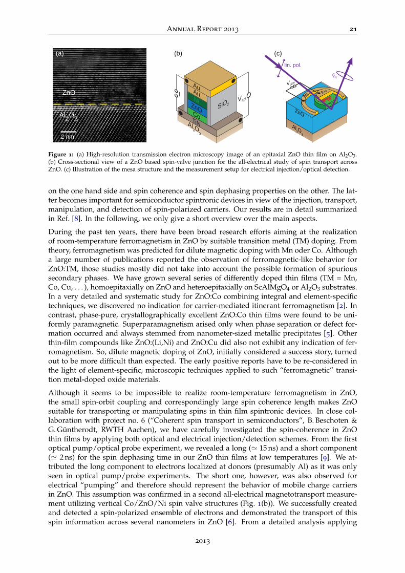
In close collaboration with various project partners in SPP 1285, we have comprehensivelyinvestigated the material system ZnO, making extensive use of our thin film fabrication labs.With funding from the priority program, we equipped our existing ultra-high vacuum lasermolecular beam epitaxy (laser-MBE) system with (i) an upgraded flexible ultra-violet laserbeam optics allowing for the precise variation of the laser fluence, (ii) an upgraded infraredlaser heating system allowing for both high substrate temperatures in UHV environment andrapid temperature changes, and (iii) a new radical source for atomic oxygen and nitrogen [7].We have optimized the deposition parameters for doped and undoped ZnO single thin films,ZnO buffer layers, and ZnO-based multilayer structures. The detailed structural characteri-zation by X-ray and transmission electron microscopy (TEM) analysis showed (see Fig. 1(a))that epitaxial ZnO thin films with high structural quality can be achieved on (0001)-orientedAl2O3 substrates, in spite of the large lattice mismatch of 18% [7]. We have also realizedthe heteroepitaxial growth of ZnO based multilayers as a prerequisite for spin transport ex-periments and the fabrication of spintronic devices [6, 7]. Our research project aimed at themagnetic properties and the possibility of dilute magnetic doping with transition metal ions
1This work is supported by the German Research Foundation via the Priority Program SPP 1285 (projectnumber GR 1132/14).
© Walther-Meißner-Institut
Annual Report 2013 21
ZnO
Al2O
3
j
m Co
Co
lin. pol.
çK
Vbias
Au
2 nm
ZnO
Al O2 3Co
ZnONiAuAu
TiNAl2O
3
SiO2V4pt
I
(a) (b) (c)
Figure 1: (a) High-resolution transmission electron microscopy image of an epitaxial ZnO thin film on Al2O3.(b) Cross-sectional view of a ZnO based spin-valve junction for the all-electrical study of spin transport acrossZnO. (c) Illustration of the mesa structure and the measurement setup for electrical injection/optical detection.
on the one hand side and spin coherence and spin dephasing properties on the other. The lat-ter becomes important for semiconductor spintronic devices in view of the injection, transport,manipulation, and detection of spin-polarized carriers. Our results are in detail summarizedin Ref. [8]. In the following, we only give a short overview over the main aspects.
During the past ten years, there have been broad research efforts aiming at the realizationof room-temperature ferromagnetism in ZnO by suitable transition metal (TM) doping. Fromtheory, ferromagnetism was predicted for dilute magnetic doping with Mn oder Co. Althougha large number of publications reported the observation of ferromagnetic-like behavior forZnO:TM, those studies mostly did not take into account the possible formation of spurioussecondary phases. We have grown several series of differently doped thin films (TM = Mn,Co, Cu, . . . ), homoepitaxially on ZnO and heteroepitaxially on ScAlMgO4 or Al2O3 substrates.In a very detailed and systematic study for ZnO:Co combining integral and element-specifictechniques, we discovered no indication for carrier-mediated itinerant ferromagnetism [2]. Incontrast, phase-pure, crystallographically excellent ZnO:Co thin films were found to be uni-formly paramagnetic. Superparamagnetism arised only when phase separation or defect for-mation occurred and always stemmed from nanometer-sized metallic precipitates [5]. Otherthin-film compounds like ZnO:(Li,Ni) and ZnO:Cu did also not exhibit any indication of fer-romagnetism. So, dilute magnetic doping of ZnO, initially considered a success story, turnedout to be more difficult than expected. The early positive reports have to be re-considered inthe light of element-specific, microscopic techniques applied to such “ferromagnetic” transi-tion metal-doped oxide materials.
Although it seems to be impossible to realize room-temperature ferromagnetism in ZnO,the small spin-orbit coupling and correspondingly large spin coherence length makes ZnOsuitable for transporting or manipulating spins in thin film spintronic devices. In close col-laboration with project no. 6 (“Coherent spin transport in semiconductors”, B. Beschoten &G. Güntherodt, RWTH Aachen), we have carefully investigated the spin-coherence in ZnOthin films by applying both optical and electrical injection/detection schemes. From the firstoptical pump/optical probe experiment, we revealed a long (' 15 ns) and a short component(' 2 ns) for the spin dephasing time in our ZnO thin films at low temperatures [9]. We at-tributed the long component to electrons localized at donors (presumably Al) as it was onlyseen in optical pump/probe experiments. The short one, however, was also observed forelectrical “pumping” and therefore should represent the behavior of mobile charge carriersin ZnO. This assumption was confirmed in a second all-electrical magnetotransport measure-ment utilizing vertical Co/ZnO/Ni spin valve structures (Fig. 1(b)). We successfully createdand detected a spin-polarized ensemble of electrons and demonstrated the transport of thisspin information across several nanometers in ZnO [6]. From a detailed analysis applying
2013
22 Walther–Meißner–Institut
a two-spin channel model with spin-dependent interface resistances, we have derived a spinlifetime of 2.6 ns for these itinerant spins at low temperatures [6]. All these data agreed wellwith the results of our third combined electrical pump/optical probe experiment (Fig. 1(c))where we found a spin dephasing time of ' 1 ns [8].
References
[1] A. Nielsen, A. Brandlmaier, M. Althammer, W. Kaiser, M. Opel, J. Simon, W. Mader, S. T. B. Goennenwein,and R. Gross, Appl. Phys. Lett. 93, 162510 (2008).
[2] M. Opel, K.-W. Nielsen, S. Bauer, S. Goennenwein, J. Cezar, D. Schmeisser, J. Simon, W. Mader, and R. Gross,Eur. Phys. J. B 63, 437–444 (2008).
[3] D. Venkateshvaran, W. Kaiser, A. Boger, M. Althammer, M. S. R. Rao, S. T. B. Goennenwein, M. Opel, and R.Gross, Phys. Rev. B 78, 092405 (2008).
[4] D. Venkateshvaran, M. Althammer, A. Nielsen, S. Geprägs, M. S. Ramachandra Rao, S. T. B. Goennenwein,M. Opel, and R. Gross, Phys. Rev. B 79, 134405 (2009).
[5] A. Ney, M. Opel, T. C. Kaspar, V. Ney, S. Ye, K. Ollefs, T. Kammermeier, S. Bauer, K.-W. Nielsen, S. T. B.Goennenwein, M. H. Engelhard, S. Zhou, K. Potzger, J. Simon, W. Mader, S. M. Heald, J. C. Cezar, F. Wilhelm,A. Rogalev, R. Gross, and S. A. Chambers, New J. Phys. 12, 013020 (2010).
[6] M. Althammer, E.-M. Karrer-Müller, S. T. B. Goennenwein, M. Opel, and R. Gross, Appl. Phys. Lett. 101,082404 (2012).
[7] M. Opel, S. Geprägs, M. Althammer, T. Brenninger, and R. Gross. Laser molecular beam epitaxy of ZnO thinfilms and heterostructures. Accepted for publication in J. Phys. D: Appl. Phys., arXiv:1307.1616 (2014).
[8] M. Opel, S. T. B. Goennenwein, M. Althammer, K.-W. Nielsen, E.-M. Karrer-Müller, S. Bauer, K. Senn, C.Schwark, C. Weier, G. Güntherodt, B. Beschoten, and R. Gross. Zinc Oxide - From Dilute Magnetic Dopingto Spin Transport. Accepted for publication in Phys. Stat. Sol. B, arXiv:1309.5857 (2014).
[9] S. Kuhlen, R. Ledesch, R. de Winter, M. Althammer, S. T. B. Goennenwein, M. Opel, R. Gross, T. A. Wassner,M. S. Brandt, and B. Beschoten. Unambiguous determination of spin dephasing times in ZnO. Submittedfor publication in Phys. Stat. Sol. B, arXiv:1309.6600 (2014).
[10] K.-W. Nielsen. Ursache der magnetischen Kopplung in Kobalt-dotiertem ZnO. Phd thesis, TU München (2008).[11] A. Nielsen. Magnetit – ein Material für die Spinelektronik. Phd thesis, TU München (2009).[12] M. K. Althammer. Spin-transport-phenomena in metals, semiconductors, and insulators. Phd thesis, TU München
(2012).
© Walther-Meißner-Institut
Annual Report 2013 23
Second Funding Period for the DFG Priority Program SPP 1458“Superconductivity in Iron-Based Compounds”
R. Hackl 1
In June 2013 the German Research Foundation (DFG) decided to support the Priority Pro-gram SPP 1450 “Superconductivity in Iron-Based Compounds” for another three years until2016. The funding includes support for approximately 25 research groups in Germany andenables them to organize one workshop, two international conferences, and several mini-workshops for the participating students. One of the coordinators (R.H.) is affiliated with theWalther-Meißner-Institute (WMI) and is principal investigator of the project “Raman study ofthe interrelation of electron dynamics and phase transitions in iron-based superconductors”(HA 2071/7-2).
T
electron dopinghole
p
SDW
SC
SC SCBa1‐xKxFe2As2 Ba(Fe1‐xCox)2As2
BaFe2(As1‐xPx)2
(a) (b)
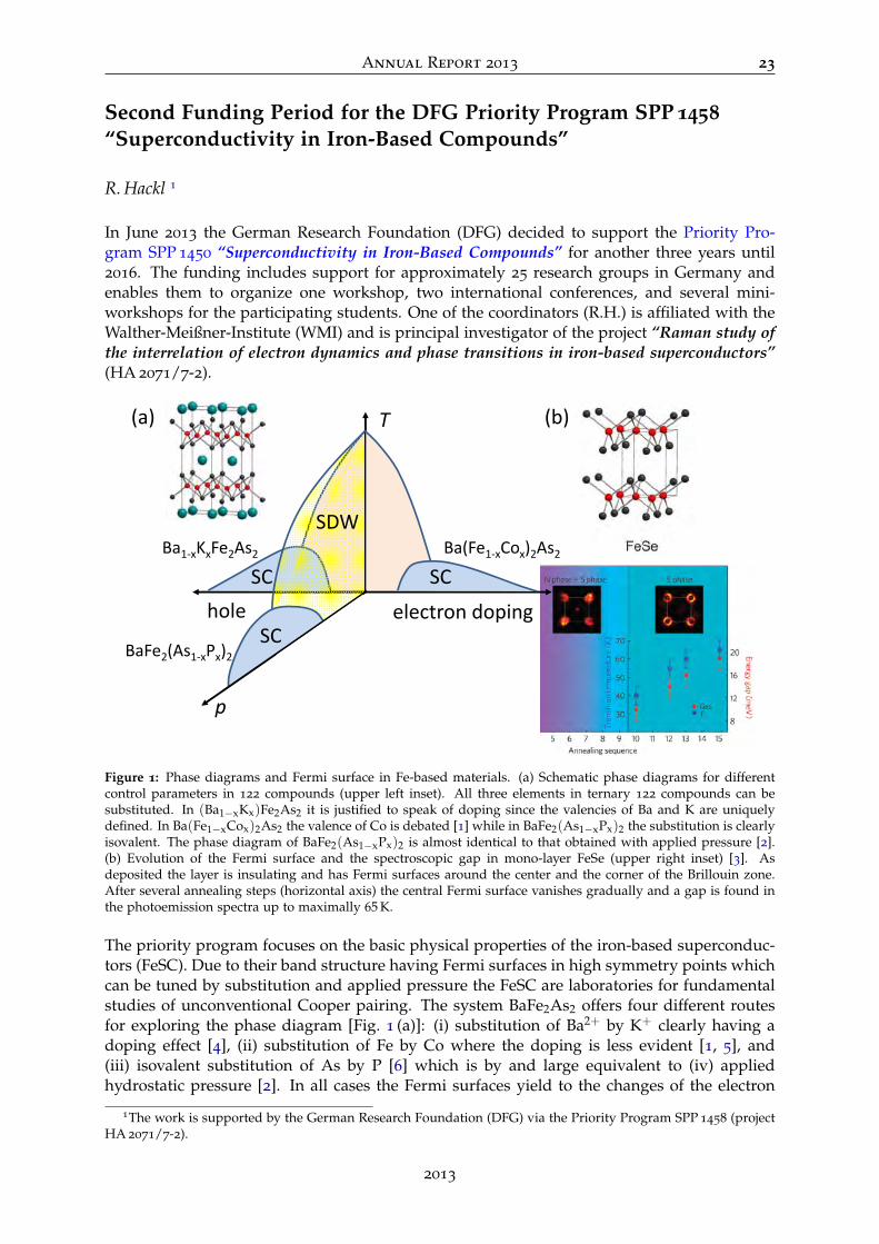
Figure 1: Phase diagrams and Fermi surface in Fe-based materials. (a) Schematic phase diagrams for differentcontrol parameters in 122 compounds (upper left inset). All three elements in ternary 122 compounds can besubstituted. In (Ba1−xKx)Fe2As2 it is justified to speak of doping since the valencies of Ba and K are uniquelydefined. In Ba(Fe1−xCox)2As2 the valence of Co is debated [1] while in BaFe2(As1−xPx)2 the substitution is clearlyisovalent. The phase diagram of BaFe2(As1−xPx)2 is almost identical to that obtained with applied pressure [2].(b) Evolution of the Fermi surface and the spectroscopic gap in mono-layer FeSe (upper right inset) [3]. Asdeposited the layer is insulating and has Fermi surfaces around the center and the corner of the Brillouin zone.After several annealing steps (horizontal axis) the central Fermi surface vanishes gradually and a gap is found inthe photoemission spectra up to maximally 65 K.
The priority program focuses on the basic physical properties of the iron-based superconduc-tors (FeSC). Due to their band structure having Fermi surfaces in high symmetry points whichcan be tuned by substitution and applied pressure the FeSC are laboratories for fundamentalstudies of unconventional Cooper pairing. The system BaFe2As2 offers four different routesfor exploring the phase diagram [Fig. 1 (a)]: (i) substitution of Ba2+ by K+ clearly having adoping effect [4], (ii) substitution of Fe by Co where the doping is less evident [1, 5], and(iii) isovalent substitution of As by P [6] which is by and large equivalent to (iv) appliedhydrostatic pressure [2]. In all cases the Fermi surfaces yield to the changes of the electron
1The work is supported by the German Research Foundation (DFG) via the Priority Program SPP 1458 (projectHA 2071/7-2).
2013
24 Walther–Meißner–Institut
count and the structure. In addition, the various substitutions influence the mean free pathof the carriers in different ways since they are at different distances from the relevant Fe lay-ers. However, in all cases the shapes of the Fermi surfaces have a crucial influence on thesuperconducting and magnetic properties. This influence becomes particularly clear in thechalcogenide FeSe [Fig. 1 (b)]. Here, a single layer FeSe on buffered SrTiO3 shows spectro-scopic evidence of superconductivity if the Fermi surface is tuned so as to solely encircle thecorners of the Brillouin zone. Then a gap is found in the photoemission spectra which closesat approximately 65 K in samples that underwent appropriate annealing protocols and reachesroughly 6kBTc at low temperature [3]. If transport and magnetization measurements can cor-roborate the conjectures from photoemission spectroscopy mono-layer FeSe would break thecurrent record of SmFeAsO reaching 56 K [7] and bring the chalcogenides closer to the centerof future activities.
The project at the WMI focuses on electronic properties in both the magnetic and the su-perconducting state. One of the new developments is the detwinning device for the systemBa(Fe1−xCox)2As2 which undergoes a structural phase transition for x ≤ 0.065. In detwinnedsamples the properties in the spin-density-wave (SDW), phase which is established a fewdegrees below the structural transition, can be studied with light polarizations parallel andperpendicular to the SDW ordering vector, returning clear anisotropies in both the electronicand lattice properties. In addition, the evolution of nematic fluctuations as one of the putativedriving forces of the phase transitions and even superconductivity can be studied in moredetail. The superconducting response in (Ba1−xKx)Fe2As2 allows insight into the momentumdependence of the pairing potential Vk,k′ via excitonic modes inside the gap (contributionby T. Böhm in this Annual Report). These modes which were predicted by Bardasis andSchrieffer [8] and studied in some detail in the context of light scattering [9–11], facilitate thequantification of anisotropies in the pairing potential and were found to be the litmus testfor competing s- and d-wave ground states in the FeSCs [12–14]. Hence the Raman experi-ment can contribute to tracking down the changes in Vk,k′ as a function of the Fermi surfacetopology.
References
[1] H. Wadati, I. Elfimov, and G. A. Sawatzky, Phys. Rev. Lett. 105, 157004 (2010).[2] E. Colombier, S. L. Bud’ko, N. Ni, and P. C. Canfield, Phys. Rev. B 79, 224518 (2009).[3] S. He, J. He, W. Zhang, L. Zhao, D. Liu, X. Liu, D. Mou, Y.-B. Ou, Q.-Y. Wang, Z. Li, L. Wang, Y. Peng, Y.
Liu, C. Chen, L. Yu, G. Liu, X. Dong, J. Zhang, C. Chen, Z. Xu, X. Chen, X. Ma, Q. Xue, and X. J. Zhou, Nat.Mater. 12, 605 (2013).
[4] M. Rotter, M. Tegel, and D. Johrendt, Phys. Rev. Lett. 101, 107006 (2008).[5] A. S. Sefat, R. Jin, M. A. McGuire, B. C. Sales, D. J. Singh, and D. Mandrus, Phys. Rev. Lett. 101, 117004
(2008).[6] J. G. Analytis, J.-H. Chu, R. D. McDonald, S. C. Riggs, and I. R. Fisher, Phys. Rev. Lett. 105, 207004 (2010).[7] K. Ishida, Y. Nakai, and H. Hosono, J. Phys. Soc. Jpn 78, 062001 (2009).[8] A. Bardasis, and J. R. Schrieffer, Phys. Rev. 121, 1050–1062 (1961).[9] A. Zawadowski, J. Ruvalds, and J. Solana, Phys. Rev. A 5, 399–421 (1972).
[10] M. V. Klein, and S. B. Dierker, Phys. Rev. B 29, 4976 (1984).[11] H. Monien, and A. Zawadowski, Phys. Rev. B 41, 8798 (1990).[12] D. J. Scalapino, and T. P. Devereaux, Phys. Rev. B 80, 140512 (2009).[13] F. Kretzschmar, B. Muschler, T. Böhm, R. Hackl, H.-H. Wen, V. Tsurkan, J. Deisenhofer, and A. Loidl. Fermi-
ology and pairing in iron-based superconductors. In WMI Annual Report, 53 (2012).[14] F. Kretzschmar, B. Muschler, T. Böhm, A. Baum, R. Hackl, H.-H. Wen, V. Tsurkan, J. Deisenhofer, and A.
Loidl, Phys. Rev. Lett. 110, 187002 (2013).
© Walther-Meißner-Institut

Annual Report 2013 25
The DFG Priority Program SPP 1538 “Spin Caloric Transport”
S. T. B. Goennenwein, R. Gross, M. Schreier, S. Meyer, J. Lotze, M. Weiler, M. Althammer,H. Huebl, M. Opel, S. Geprägs 1
The field of spin caloritronics addresses the impact of the spin de-gree of freedom on the thermally driven transport properties ofsolid state systems [1]. A few years ago, the notion emerged thatspin caloritronic phenomena are much more than spin-dependentreplica of the well-established, thermo-galvanic effects. One keyinsight from the ensuing research activities is that spin-dependententropy transport does not necessarily require mobile charge car-riers. Rather, entropy transport also is possible via spin excita-tions (magnons), resulting in a new set of spin caloritronic phe-nomena such as the spin Seebeck effect [2] or the spin Nernst ef-fect [3]. Since magnons are present in conductive ferromagnetsjust as well as in so-called magnetic insulators – i.e., in electri-cally insulating materials exhibiting long-range ferromagnetic orferrimagnetic order – the new spin caloritronic effects just men-tioned will be present in particular also in magnetic insulators. In contrast, the conventional,charge-based thermo-galvanic effects must vanish in these materials, since magnetic insula-tors do not contain mobile charges. Magnon-based spin caloritronic effects thus indeed arequalitatively different from the long-known, charge-based thermo-galvanic phenomena.
To stimulate research activities on spin caloric phenomena, the German Research Foundation(DFG) has launched the Priority Program SPP 1538 entitled Spin Caloric Transport (SpinCaT)in 2011. The aim of SPP 1538 is to develop the new research field of spin-related caloriceffects. The Walther-Meißner-Institute (WMI) participates in this program with the projectSpin-dependent Thermo-galvanic Effects. As the first three-year funding period will end inmid 2014, we have already submitted a renewal proposal for the second three year fundingperiod. One focus of our spin caloric transport research activities is on spatially resolved spincaloritronic experiments. As detailed in Ref. [4], we use a focused laser beam to generatea local thermal gradient in magnetic thin films or hybrid heterostructures, and investigatethe resulting spin caloritronic responses [5]. This technique in particular enables spatiallyresolved spin Seebeck effect measurements in magnetic insulator/normal metal hybrids. Wehave pursued and extended this approach, taking advantage of the excellent yttrium irongarnet (Y3Fe5O12, YIG) thin films grown via laser-MBE in house at WMI [6]. This year, wehave substantiated the spatially resolved spin Seebeck experiments by a detailed calculationof the thermal profiles arising in YIG/normal metal hybrids upon laser illumination [7, 8].We furthermore have quantitatively compared the magnitude of the spin Seebeck effect ob-served experimentally in these structures with related, magnon-current based phenomena,namely the spin pumping effect and the spin Hall magnetoresistance [9]. In the second lineof experiments, we have extensively investigated the spin Hall magnetoresistance that we re-cently discovered in YIG/Pt-type hybrid structures [5, 10–12]. As discussed in more detailin the contribution by Meyer et al. on page 57, the spin Hall magnetoresistance arises fromthe interplay between charge currents flowing in the normal metal (Pt) with magnon currents(spin currents) flowing in the magnetic insulator (YIG), and thus is closely related to the ther-mally driven magnon currents observed in spin Seebeck measurements in these structures.It also is important to emphasize that our spin caloritronic experiments viz. their theoretical
1This work is supported by the German Research Foundation via Priority Program SPP 1538 (project numberGO 944/4-1).
2013

26 Walther–Meißner–Institut
interpretation are performed in close collaboration with the groups of Prof. E. Saitoh andProf. G. E. W. Bauer from the Institute for Materials Research, Tohoku University, Sendai,Japan, as well as with collaboration partners within SPP 1538.
Currently, we work towards time-resolved spin Seebeck effect experiments in our YIG/Pthybrid structures, aiming to identify the microscopic mechanisms responsible for the effect.Another important line of work deals with the fabrication and investigation of magnetic insu-lators exhibiting a magnetic compensation point, such as gadolinium iron garnet (Gd3Fe5O12)or dysprosium iron garnet (Dy3Fe5O12). At a certain temperature (the compensation temper-ature), the magnetic moments of the different magnetic sublattices in these materials cancelout exactly. The materials then behave like antiferromagnets in many aspects, enabling ex-ploratory studies of spin caloritronic phenomena in this regime.
References
[1] G. E. W. Bauer, E. Saitoh, and B. J. van Wees, Nat. Mater. 11, 391–399 (2012).[2] K. Uchida, J. Xiao, H. Adachi, J. Ohe, S. Takahashi, J. Ieda, T. Ota, Y. Kajiwara, H. Umezawa, H. Kawai,
G. E. W. Bauer, S. Maekawa, and E. Saitoh, Nat. Mater. 9, 894–897 (2010).[3] K. Tauber, M. Gradhand, D. V. Fedorov, and I. Mertig, Phys. Rev. Lett. 109, 026601 (2012).[4] M. Weiler, M. Schreier, M. Althammer, S. Meyer, H. Huebl, M. Opel, S. Geprägs, R. Gross, S. T. B. Goennen-
wein, I.-M. Imort, G. Reiss, and A. Thomas. Spin and Charge Currents in Magneto-thermal Landscapes. InWMI Annual Report, 68 (2012).
[5] M. Weiler, M. Althammer, F. D. Czeschka, H. Huebl, M. S. Wagner, M. Opel, I.-M. Imort, G. Reiss, A. Thomas,R. Gross, and S. T. B. Goennenwein, Phys. Rev. Lett. 108, 106602 (2012).
[6] M. Althammer, M. S. Wagner, J. Lotze, H. Huebl, S. T. B. Goennenwein, and M. Opel. Epitaxial Yttrium-Iron-Garnet (YIG) Thin Films. In WMI Annual Report, 75 (2011).
[7] M. Schreier, A. Kamra, M. Weiler, J. Xiao, G. E. W. Bauer, R. Gross, and S. T. B. Goennenwein, Phys. Rev. B88, 094410 (2013).
[8] M. Schreier, N. Roschewsky, E. Dobler, S. Meyer, H. Huebl, R. Gross, and S. T. B. Goennenwein, Appl. Phys.Lett. 103, 242404 (2013).
[9] M. Weiler, M. Althammer, M. Schreier, J. Lotze, M. Pernpeintner, S. Meyer, H. Huebl, R. Gross, A. Kamra, J.Xiao, Y.-T. Chen, H. Jiao, G. E. W. Bauer, and S. T. B. Goennenwein, Phys. Rev. Lett. 111, 176601 (2013).
[10] H. Nakayama, M. Althammer, Y.-T. Chen, K. Uchida, Y. Kajiwara, D. Kikuchi, T. Ohtani, S. Geprägs, M.Opel, S. Takahashi, R. Gross, G. E. W. Bauer, S. T. B. Goennenwein, and E. Saitoh, Phys. Rev. Lett. 110,206601 (2013).
[11] M. Althammer, S. Meyer, H. Nakayama, M. Schreier, S. Altmannshofer, M. Weiler, H. Huebl, S. Geprägs, M.Opel, R. Gross, D. Meier, C. Klewe, T. Kuschel, J.-M. Schmalhorst, G. Reiss, L. Shen, A. Gupta, Y.-T. Chen,G. E. W. Bauer, E. Saitoh, and S. T. B. Goennenwein, Phys. Rev. B 87, 224401 (2013).
[12] Y.-T. Chen, S. Takahashi, H. Nakayama, M. Althammer, S. T. B. Goennenwein, E. Saitoh, and G. E. W. Bauer,Phys. Rev. B 87, 144411 (2013).
© Walther-Meißner-Institut
Annual Report 2013 27
The EU Marie Curie Initial Training Network “Circuit and CavityQuantum Electrodynamics (CCQED)”
F. Deppe, R. Gross, A. Marx 1
The key objective of the european network Circuit and CavityQuantum Electro-Dynamics (CCQED) is to investigate the cou-pling between light and matter at its most fundamental level,where one or a few atoms strongly interact with a single mode ofthe electromagnetic field stored in a resonator containing a smallnumber of photons. This research area, named Cavity QuantumElectrodynamics, has been at first investigated with real atoms coupled to microwave or op-tical photons. However, the recent years showed that the very same physics can be studiedin a solid-state architecture, nicknamed Circuit Quantum Electrodynamics, where now artifi-cial atoms made of Josephson junctions are coupled to on-chip superconducting resonators.Both fields made spectacular progress in the past years, with a remarkable diversity of demon-strated physical effects. To list a few, milestones include the direct observation of the quantumjumps of microwave light, the deterministic generation and tomography of arbitrary quantumstates of a resonator by superconducting quantum bits, the evidence of the lamb shift in asolid-state system, the generation of nonlinear photonics with one atom, and the realizationof feedback schemes on single atoms triggered by the detection of single photons.
In 2011, the european network Circuit and Cavity Quantum Electro-Dynamics (CCQED) hasbeen granted 3.5 Million Euros by the European Union through a Marie Curie Action withinthe Seventh Framework Program Initial Training Network ITN-People-2010. The aim of CC-QED is to bridge two communities in physics, in the academic and private sectors, to share,pursue and diffuse within Europe the benefits of collaborations in the science of elementaryquanta. CCQED involves 10 research centres and 3 companies, representing the cutting edgeof research in the quantum electrodynamics of fundamental systems in Europe. The networktrains 12 early stage researchers (Ph.D. students) and 2 experienced researchers (postdocs).They focus on establishing bonds between solid-state and quantum optics physics, strength-ening the communication between theory and experiment, and establishing links betweenfundamental and applied research. Prominent scientists and industry leaders contribute tothe schools and workshops. Special attention is given to the development of complementaryskills, such as communication, presentation, project planning, and management. The WMIcontributes with its expertise on the design, fabrication, and measurement of superconduct-ing quantum circuits. In particular, the focus lies on the exploration of quantum correlationsin the important microwave frequency domain.
At the WMI, we perform experimental studies on propagating microwaves generated us-ing superconducting quantum circuits in a cryogenic environment [1–3]. We demonstratedswitchable coupling between two niobium transmission line resonators (TLR) mediated by asuperconducting flux qubit [4, 5]. For fixed coupling, we investigated the distributed cou-pling [6] and developed a layout for scalable chains of TLR [7, 8]. Transmission measurementsyielded consistent parameters for up to three coupled TLR. These experiments are the basisfor more elaborate studies on thermal entanglement, entanglement scaling laws, and, moregenerally, analog quantum simulations. Furthermore, we measured propagating squeezed mi-crowave light generated by a flux-driven Josephson parametric amplifier. We can consistentlydetect squeezing [9] by using either a single path and sideband mixing or a beam splitter anddual-path state tomography [1–3, 10]. In the latter case, we demonstrated entanglement with
1This work is supported by the EU projects CCQED.
2013

28 Walther–Meißner–Institut
respect to the two beam splitter output paths. Based on this work, we plan teleportation withcontinuous-variable quantum microwaves.
From September 09 to 13, 2013,CCQED has organized theInternational Conference onResonator QED. It took placeat the Kardinal Wendel Hausclose to the English Garden inMunich-Schwabing (organizers:Peter Domokos (Wigner), RudolfGross (WMI), Gerhard Rempe(MPQ) & Tatjana Wilk (MPQ)).It was focussing on (i) singleatom cavity QED, (ii) multi-atomcavity QED, (iii) circuit QED, (iv)
photonic crystal cavity QED, (v) quantum information processing with CCQED systems, (vi)cavity optomechanics, (vii) hybrid circuit or cavity QED systems, and (viii) QED withoutcavity. With more than 140 participants from all over the world, the conference was a majorand very successful event. The final programme comprised 6 tutorials, 28 invited talks, 18
contributed talks and 57 posters. The local CCQED network partners (Max-Planck-Institutefor Quantum Optics and Walther-Meißner-Institute) opened doors for a tour through theirlaboratories. Moreover, the CCQED industry partners invited conference attendees to visittheir facilities or offer to meet their experts. To disseminate research on quantum optics andcircuit QED to a broader public, CCQED organized an evening with a public lecture by Nobellaureate in physics, Serge Haroche on 11
th September at the Ehrensaal of the Deutsches Mu-seum. Subsequently, a panel discussion (presented by Jeanne Rubner, Bayerischer Rundfunk)on “Research & Innovation” with guests from research, politics and industry examined thelink between basic research and innovation. The event attracted more than 150 participants.
The EU small or medium-scale focused research project “Quan-tum Propagating Microwaves in Strongly Coupled Environments(PROMISCE)”
F. Deppe, R. Gross, A. Marx 2
The EU Collaborative Project entitled Quantum Propagating Mi-crowaves in Strongly Coupled Environments – PROMISCE isfunded by the FET-Open Initiative of the EU 7
th Framework Pro-gram since early 2012. It studies the dynamics of microwave pho-tons in quantum circuits, including their interaction with super-conducting qubits, transmission lines and quantum metamateri-als. The aim of PROMISCE is to provide the foundations for a novel research field: propa-gating quantum microwave technologies in strongly and ultrastrongly coupled environments.It emerged from the challenging and controversial idea that microwave photons can inter-act strongly among each other and with their environment, even in the absence of confiningcavities. PROMISCE combines two major innovative and interdisciplinary components. Thefirst one, propagating quantum microwave photonics, focuses on the generation, control, and
2This work is supported by the EU project PROMISCE.
© Walther-Meißner-Institut

Annual Report 2013 29
detection of quantum microwave beams and photons using superconducting quantum cir-cuits. The second one aims at the exploration of interactions between propagating quantummicrowaves and their potential for quantum information processing. The ultimate goal ofPROMISCE is to merge the possibilities of all-optical quantum computing with supercon-ducting circuits. The result should be quantum networks [7, 8] that perform useful tasks suchas scalable quantum gates or quantum simulation of condensed matter and field quantumtheory problems [11].
The research efforts at WMI employ superconducting quantum circuits to explore novel pathsin engineering strong and ultrastrong controlled interactions [12] between propagating mi-crowave photons and their environment as well as among photons themselves. To this end,we aim at the development and understanding of microwave beam splitters [6, 13], whichare an essential component in the manipulation of propagating photons and in particular forthe implementation of single-qubit gates in travelling qubits. Recently, we have witnessed thedevelopment of tunable beam splitters in the optical regime, a novel tool which allows one todynamically control those single qubit gates. Within PROMISCE we develop microwave beamsplitters with a similar degree of tunability. Another research direction within PROMISCE isthe development of a deterministic single photon source, which can be realized either by a reli-ably controlled superconducting qubit in a leaky cavity or a superconducting qubit in an openline with some transverse driving. As WMI is an early player in the field of quantum propa-gating microwave, it contributes with pronounced experimental expertise to PROMISCE.
References
[1] E. P. Menzel, R. Di Candia, F. Deppe, P. Eder, L. Zhong, M. Ihmig, M. Haeberlein, A. Baust, E. Hoffmann,D. Ballester, K. Inomata, T. Yamamoto, Y. Nakamura, E. Solano, A. Marx, and R. Gross, Phys. Rev. Lett. 109,250502 (2012).
[2] E. P. Menzel, F. Deppe, M. Mariantoni, M. A. Araque Caballero, A. Baust, T. Niemczyk, E. Hoffmann, A.Marx, E. Solano, and R. Gross, Phys. Rev. Lett. 105, 100401 (2010).
[3] E. P. Menzel. Propagating Quantum Microwaves: Dual-path State Reconstruction and Path Entanglement. Disser-tation, Technische Universität München (2013).
[4] E. Hoffmann. Experiments on Two-Resonator Circuit Quantum Electrodynamics: A Superconducting QuantumSwitch. Ph.D. thesis, TU München (2013).
[5] M. Mariantoni, F. Deppe, A. Marx, R. Gross, F. Wilhelm, and E. Solano, Phys. Rev. B 78, 104508 (2008).[6] B. Peropadre, D. Zueco, F. Wulschner, F. Deppe, A. Marx, R. Gross, and J. Garcia-Ripoll, Phys. Rev. B 87,
134504 (2013).[7] M. Leib, and M. J. Hartmann, New J. of Phys. 12, 093031 (2010).[8] M. Leib, F. Deppe, A. Marx, R. Gross, and M. J. Hartmann, New Journal of Physics 14, 075024 (2012).[9] L. Zhong, E. P. Menzel, R. D. Candia, P. Eder, M. Ihmig, A. Baust, M. Haeberlein, E. Hoffmann, K. Inomata,
T. Yamamoto, Y. Nakamura, E. Solano, F. Deppe, A. Marx, and R. Gross, New Journal of Physics 15, 125013
(2013).[10] R. Di Candia, E. P. Menzel, L. Zhong, F. Deppe, A. Marx, R. Gross, and E. Solano. Dual-Path Methods for
Propagating Quantum Microwaves. Accepted for publication in New J. of Phys., arXiv:1308.3117 (2013).[11] D. Ballester, G. Romero, J. J. Garcia-Ripoll, F. Deppe, and E. Solano, Phys. Rev. X 2, 021007 (2012).[12] T. Niemczyk, F. Deppe, H. Huebl, E. P. Menzel, F. Hocke, M. J. Schwarz, J. J. Garcia-Ripoll, D. Zueco, T.
Hummer, E. Solano, A. Marx, and R. Gross, Nat Phys 6, 772–776 (2010).[13] M. Haeberlein, D. Zueco, P. Assum, E. Hoffmann, B. Peropadre, J. Garcia-Ripoll, E. Solano, F. Deppe, A.
Marx, and R. Gross. Fast microwave beam splitters from superconducting resonators. Submitted for publi-cation, arXiv:1302.0729 (2013).
2013
30 Walther–Meißner–Institut
© Walther-Meißner-Institut

Basic Research
500 μm
nano-beam: ø ≈ 100 nm
20 μm
microwave resonator
Microwave box (top left) containing a chip with several superconducting coplanar waveguide resonators (topright). The image at the bottom shows an enlarged view of one end of a microwave resonator, where an about100 nm wide Si3N4/Nb nanobeam is coupled to the ground plane of the resonator.
31


Annual Report 2013 33
Time-domain Experiments on the Quantum Switch
A. Baust, E. Hoffmann, M. Haeberlein, P. Eder, H. Huebl, E. Menzel, F. Deppe, A. Marx,R. Gross1
D. Zueco2, J.-J. Garcia-Ripoll3, E. Solano4
During the last decade, superconducting coplanar waveguide resonators and quantum bits(qubits) have not only proven to provide a highly flexible toolbox for the realization of ex-periments giving deep insight into light-matter interaction physics [1, 2], but are also verypromising building blocks for future quantum computing and quantum simulation architec-tures. However, the successful realization of the latter will not only require to increase thenumber of qubits and resonators used in the setup, but will also require tunable and switch-able coupling between these building blocks.
AB,dyng
AB,geog
A BQ
(a)
498 500 502
4
6
8
5
7
9
Dev
iatio
n of
Mag
nitu
de (d
B)
−4
−2
0
2
4
Flux (m )0
f (G
Hz)
S
498 499 500 501 502 503
4.87
4.88
4.89
4.9
4.91
4.92
Mag
nitu
de (d
B)
-140-130-120-110-100-90-80
0Flux (m )
f (G
Hz)
(b)
30 µm
Flux (m )
f (G
Hz)
498 499 500 501 502 503
4.88
4.89
4.9
4.91
Mag
nitu
de (d
B)
-140
-130
-120
-110
-100
-90
-80
0
(c)
(d) (e)
ext
Figure 1: (a) Sketch of the quantum switch with the qubit Q coupled to the resonators A and B. The couplingbetween the resonators is determined by the dynamical and geometric coupling rates. (b) False-color SEM micro-graph of the flux qubit (red) coupled galvanically to the resonators (green). (c) Qubit parameters are extractedfrom a two-tone spectroscopy measurement. (d) Transmission measured through one of the resonators dependingon the magnetic flux and frequency with the qubit in the ground state. The crossings defining the switch set-ting conditions between the two resonant modes are observed. (e) Same transmission measurement for a drivenqubit. No crossing between the modes is observed, indicating that the coupling between the resonators is presentindependent of the applied magnetic flux. (a)-(e) These figures are taken from Ref. [3].
Our approach to realize tunable coupling between two microwave resonators is the quantumswitch [4] which consists of a three-Josephson-junction flux qubit coupled galvanically to twohalf-wave resonators, cf. Fig. 1(a-b). In this setup, two coupling mechanisms between the res-onators have to be considered. The geometric coupling ggeo is determined solely by the circuit
1This work is supported by the German Research Foundation via SFB 631, the German Excellence Initiativevia NIM, the EU Marie Curie Initial Training Network CCQED and the EU Specific Targeted Research ProgramPROMISCE.
2CSIC-Universidad de Zaragoza, Spain.3IFF-CSIC, Madrid, Spain.4Universidad del Pais Vasco UPV/EHU and Ikerbasque, Spain. E.S. acknowledges financial support by
PROMISCE, SCALEQIT, UPV/EHU UFI 11/55 Basque Government IT 472-10 and Spanish MINECO FIS2012-36673-C03-02.
2013

34 Walther–Meißner–Institut
layout, the dynamical coupling gdyn depends on the qubit state and on the qubit transition fre-quency which can be tuned by applying an external magnetic flux to the qubit loop. Themagnetic flux can be adjusted such that the dynamical coupling compensates the geomet-ric coupling, yielding zero coupling between the two resonators (defining the switch settingconditions). For a detailed description of the quantum switch, we refer to Refs. [3, 5].
The qubit parameters are extracted from two-tone spectroscopy as shown in Fig. 1(c). InFig. 1(d), the transmission through one of the two resonators depending on the magnetic fluxapplied to the qubit loop is shown. As expected for coupled harmonic oscillators, two modescan be observed. The frequency of the upper mode depends on the magnetic flux and crossesthe lower mode at the switch setting conditions. However, when the qubit is driven, thecoupling between the two resonators is present independent of the applied flux, cf. Fig. 1(e).These spectroscopic measurements already indicate that the coupling between the resonatorscan be switched on and off by driving the qubit or varying the magnetic flux.
time (µs)
ampl
itude resonator probe pulse
qubit drive pulse
30µs
10µs
resonator probe
qubit drive
chn. 1
chn. 1
chn. 1
chn. 2
(a)
(c)
(b)
0 10 20 30 40 50 0
5
10
15
20
25
30
time (µs)
tran
smis
sion
am
plitu
de (a
.u.)
Figure 2: (a) Pulse pattern for the time-domain probe of thequantum switch. The resonator probe pulse has a length of30 µs. The qubit drive pulse is delayed by 10 µs and is 10 µslong. (b) When the qubit is driven, a decrease in the output sig-nal of the probed resonator is expected as energy is transferredinto the second resonator. Simultaneously, an increase in thesecond resonator output signal is expected. (c) Measured timetraces of the output signals of the two resonators. Decrease(chn. 1) and increase (chn. 2) in the resonator output signalsare observed as expected when the qubit drive is switched on.
Here, we report on a time domain ex-periment making the switchable cou-pling directly observable. To this end,we have set a flux corresponding to theswitch setting condition and have ap-plied a probe pulse (length τres = 30 µs)to one of the resonators at the frequencyof the lower mode ωres = 4.888 GHz.Only 10 µs after applying the resonatorprobe pulse, a strong 10 µs driving pulseis applied to the qubit, switching thecoupling between the resonators on. Aschematic of the pulse sequence is de-picted in Fig. 2(a-b). The output sig-nals of both resonators are detectedtime-resolved using an FPGA-enhancedA/D-converter. The results are shownin Fig. 2(c). After switching on the qubitdrive, the output signal level of the res-onator where the drive pulse is applieddecreases, whereas it increases for theother resonator. This result represents adirect experimental evidence for the ex-pected switching behavior as the trans-fer of energy from one into another res-onator controlled by the qubit state canbe observed.
However, for an ideal quantum switch,one would expect that at the switch set-ting condition the output signal level forthe second resonator is zero when thequbit is in the ground state. Neverthe-less, in our case a finite output signallevel can be observed. We ascribe thisfinding to the fact that, due to the gal-vanic coupling, more than two resonantmodes are present in our sample (data
© Walther-Meißner-Institut
Annual Report 2013 35
not shown), giving rise to an additional coupling channel between the two resonators. Whilethe origin of these additional modes has yet to be understood in full detail, the data shownhere still provide experimental evidence for tunable and switchable coupling between twocoplanar waveguide resonators.
References
[1] A. Wallraff, D. I. Schuster, A. Blais, L. Frunzio, R.-S. Huang, J. Majer, S. Kumar, S. M. Girvin, and R. J.Schoelkopf, Nature 431, 162–167 (2004).
[2] T. Niemczyk, F. Deppe, H. Huebl, E. P. Menzel, F. Hocke, M. J. Schwarz, J. J. Garcia-Ripoll, D. Zueco, T.Hummer, E. Solano, A. Marx, and R. Gross, Nat Phys 6, 772–776 (2010).
[3] E. Hoffmann. Tunable Coupling Between Two Resonators Controlled by a Flux Qubit - The Quantum Switch.In WMI Annual Report, pp. 49–50 (2012).
[4] M. Mariantoni, F. Deppe, A. Marx, R. Gross, F. Wilhelm, and E. Solano, Phys. Rev. B 78, 104508 (2008).[5] E. Hoffmann. Experiments on Two-Resonator Circuit Quantum Electrodynamics: A Superconducting Quantum
Switch. Ph.D. thesis, TU München (2013).
2013

36 Walther–Meißner–Institut
Switching Dynamics of Electromechanically Induced Transparency
H. Huebl, F. Hocke, A. Marx, R. Gross 1
X. Zhou, A. Schliesser, T. J. Kippenberg 2,3
In the field of optomechanics, a light field trapped in an optical resonator dynamically inter-acts with a mechanical degree of freedom, enabling cooling and amplification of mechanicalmotion. This concept of light-matter interaction can be transferred to the microwave (MW)regime combining superconducting MW circuits with nanometer-sized mechanical beams, es-tablishing the class of circuit nano-electromechanics. [1–9]. In this realm, a range of optome-chanical phenomena can be explored. Amongst them are the transduction of the displacementof the mechanical oscillator on the microwave properties with a sensitivity below the level ofthe mechanical zero-point motion, the implementation of microwave sideband cooling to thequantum ground state, and electromechanical amplification of microwave signals [1, 10]. Ad-ditionally, spectroscopy of the coupled microwave-mechanical system leads to interferenceeffects such as the electromechanically induced absorption and transparency [1, 2, 11, 12].Those are important steps towards for the realization of advanced protocols including quan-tum state transfer from the microwave to the mechanical domain [7, 10–14], fast sidebandcooling [15], and routing of classical and quantum microwave signals.
In the following, we consider only the case of red-detuning (∆ = −Ωm) [1, 2] (cf. Fig. 1). In thiscase, a strong drive tone at ωd close to the lower motional sideband of the superconductingmicrowave cavity is applied to the system, while a second, much weaker tone probes themodified cavity resonance at frequency ωp = ωd + Ω. The simultaneous presence of the driveand the probe tones results in a force oscillating at Ω = ωp−ωd. If this difference frequency isclose to the mechanical resonance frequency, Ω ' Ωm, a coherent oscillation of the mechanicalsystem is induced. As a consequence of this oscillation, Stokes and anti-Stokes fields build upat ωd ±Ωm around the strong driving field. Additionally, the microwave resonator acts as anarrow-band filter for these fields. If the system is in the resolved-sideband regime, i.e. if themechanical frequency Ωm exceeds the linewidth κc of the microwave cavity, the Stokes lineat ωd −Ωm < ωc is strongly suppressed because it is off-resonant with the cavity, whereasthe anti-Stokes line at ωd + Ωm ' ωc is enhanced. Moreover, since the anti-Stokes scatteredfield is degenerate with the probe field sent to the cavity, it can lead to destructive interferenceof the two fields, preventing the build-up of an intra-cavity probe field. In consequence, weexpect an increased ”transparency” of the cavity transmission (cf. inset of Fig. 1).
To this end, we investigate the nano-electromechanical hybrid device outlined in Refs. [1, 2]comprised of a superconducting niobium microwave resonator with a resonance frequency ofωc/(2π) = 6.07 GHz and a linewidth of κc/(2π) = 742 kHz and a double layer Si3N4/Nbnanobeam with dimensions of 60 µm× 140 nm× 200 nm, a mechanical resonance frequencyΩm/(2π)) = 1.45 MHz, and a linewidth of Γm/(2π) = 9 Hz. This system thus resides inthe resolved sideband regime as Ωm > κc. The experiments are performed in a dilutionrefrigerator at approximately 170 mK to reduce the initial thermal equilibrium phonon occu-pancy in the mechanical nanobeam. At an even lower temperature, of approximately 30 mK,we observe an increase in the quality factor to 0.6× 10⁶. These temperatures are far belowthe superconducting transition temperature of Nb (9.2 K) and the thermal excitation of themicrowave cavity is significantly suppressed, as hωc/kB = 288 mK, where h is the reducedPlanck constant and kB is the Boltzmann constant.
1The authors acknowledge financial support from the German Excellence Initiative via the “Nanosystems Ini-tiative Munich‘” (NIM).
2École Polytechnique Fédérale de Lausanne (EPFL), CH-1015 Lausanne, Switzerland3T.J.K acknowledges support by the ERC grant SIMP and X.Z. by the NCCR of Quantum Engineering. Samples
were grown and fabricated at the Center of MicroNanotechnology (CMi) at EPFL.
© Walther-Meißner-Institut

Annual Report 2013 37
m
d
drive
m
anti‐Stokes
Stokes
c p
prob
e
= d – c
= p – d
-10 -5 0 5 10-40
-35
-30
-25
-20
-15
trans
mis
sion
(dB
)
(-m)/(2) (kHz)
Figure 1: Microwave excitation configuration and electromechanically induced transparency. The drive tone andthe probe tone are adjusted to the frequencies ωd and ωp, respectively. To detect electromechanically inducedtransparency, the drive tone is set to the red sideband configuration ωd = ωc −Ωm and the probe tone is sweptover the anti-Stokes line. The inset shows the resulting transmission spectra for increasing drive powers. Here, atransparency feature arises and broadens for high drive powers due to the increased effective mechanical dampingrate Γeff.
To access the switching dynamics of the device, we modulate the drive tone and investigatethe response of the probe beam in the time domain. Note, that the system’s response canbe limited both by the dynamics of the mechanical mode amplitude and by the pump field.Figure 2(a) shows the pulse sequence employed to experimentally investigate the dynamics.The continuous wave probe tone is set to the frequency ωp = ωd + Ωm and the drive toneset to ωd is modulated. Using a sufficiently long pulse, we prepare the system in a steadystate situation. After this, we pulse the drive tone with a 50% duty cycle and a pulse lengthof Ton/off.
We find, that the transmission displayed in Fig. 2(b) for short pulse times Ton/off follows themodulation of the pump tone and is determined by the characteristic time constant of the mi-crowave cavity κc. This reveals a counterintuitive regime where the relevant time constant issubstantially faster than the slowest time constant of the problem (that is, the inverse effectivemechanical damping rate, Γm). For longer Ton/off we find, that the mechanical damping rateΓm is at play as shown in Fig. 2(c). During longer ”off” configurations, the mechanical oscil-lation relaxes towards its equilibrium position at the rate of the intrinsic damping rate Γm, sowhen the pump is switched back on, the mechanical oscillation amplitude is not identical tothe steady state configuration present at the end of the preparation pulse. As a consequence,the transparency feature increases back towards its steady state value at a rate of the effec-tive damping rate Γeff, leading to a recovery to a finite probe transmission. Thus, continuousswitching is possible if the loss in the mechanical amplitude due to damping between thesuccessive pump pulses is compensated within the switching period. Note, that in the ”on”state, the transparency window amplitude depends significantly on the mechanical oscillationamplitude (see Fig. 2(b) and (c) in combination with the inset in Fig. 1). Extending the demon-strated temporal control in conjunction with probe pulses allows storage of the probe fieldthrough conversion into a coherent excitation of the mechanical oscillator [16].
To summarize, we have demonstrated that electromechanically induced transparency can beused in electromechanical systems to manipulate the transmission of a microwave signal in afully integrated architecture without the need of photon detection and regeneration. Interest-ingly, the switching can be faster than the timescale of the mechanical oscillator’s energy decayrate, a feature which is also of interest for the implementation of narrow switchable filters inthe microwave domain. Combining the system with the powerful advances in the generation
2013

38 Walther–Meißner–Institut
probe
driveoff
on
off
on
a)
b) c)
Figure 2: Dynamic response of the transparency feature for pulsed drive tone excitation. The frequencies areconfigured as outlined in Fig. 1. Panel a) displays the drive pulse sequence sent to the nano-electromechanicaldevice. The probe tone is operated in a continuous wave operation. Panel b) shows the transmission of the systemfor the on and off times (Ton/off) short as compared to (Γeff)
−1. Evidently, the system responds on much shortertimescales comparable with the inverse cavity decay rate (κc)−1 and is not limited by Γeff. For longer Ton/off wefind, that the mechanical system relaxes during the off period of the pulse, cf. panel (c). Subsequently, when thepulse is switched on again, the system reaches for its steady state value with the effective mechanical dampingrate Γeff.
and detection of single microwave photons may allow for the control over the propagation ofnon-classical states using the electromechanical architecture. Moreover, it provides the basisfor the complete storage and retrieval of a microwave quantum state in long-lived mechanicalexcitations.
References
[1] F. Hocke, X. Zhou, A. Schliesser, T. J. Kippenberg, H. Huebl, and R. Gross, New J. Phys. 14, 123037 (2012).[2] X. Zhou, F. Hocke, A. Schliesser, A. Marx, H. Huebl, R. Gross, and T. J. Kippenberg, Nat. Phys. 9, 179 (2013).[3] F. Marquardt, and S. M. Girvin, Physics 2, 40 (2009).[4] M. Aspelmeyer, S. Gröblacher, K. Hammerer, and N. Kiesel, J. Opt. Soc. Am. B 27, A189–A197 (2010).[5] C. A. Regal, and K. W. Lehnert, J. Phys.: Conf. Ser. 264, 012025 (2011).[6] M. Aspelmeyer, P. Meystre, and K. Schwab, Phys. Today 65, 29–35 (2012).[7] J. D. Teufel, D. Li, M. S. Allman, K. Cicak, A. J. Sirois, J. D. Whittaker, and R. W. Simmonds, Nature 471,
204–208 (2011).[8] T. A. Palomaki, J. W. Harlow, J. D. Teufel, R. W. Simmonds, and K. W. Lehnert, Nature 495, 210–214 (2013).[9] T. A. Palomaki, J. D. Teufel, R. W. Simmonds, and K. W. Lehnert, Science 342, 710 (2013).
[10] F. Massel, T. T. Heikkilaä, J.-M. Pirkkalainen, S. U. Cho, H. Saloniemi, P. J. Hakonen, and M. A. Sillanpää,Nature 480, 351–354 (2011).
[11] S. Weis, R. Rivière, S. Deléglise, E. Gavartin, O. Arcizet, A. Schliesser, and T. J. Kippenberg, Science 330,1520–1523 (2010).
[12] A. H. Safavi-Naeini, T. P. M. Alegre, J. Chan, M. Eichenfield, M. Winger, Q. Lin, J. T. Hill, D. E. Chang, andO. Painter, Nature 472, 69–73 (2011).
[13] O. Romero-Isart, A. C. Pflanzer, M. L. Juan, R. Quidant, N. Kiesel, M. Aspelmeyer, and J. I. Cirac, Phys. Rev.A 83, 013803 (2011).
[14] E. Verhagen, S. Delèglise, S. Weis, A. Schliesser, and T. J. Kippenberg, Nature 482, 63–67 (2012).[15] X. Wang, S. Vinjanampathy, F. W. Strauch, and K. Jacobs, Phys. Rev. Lett. 107, 177204 (2011).[16] T. A. Palomaki, J. W. Harlow, J. D. Teufel, S. R. W., and K. W. Lehnert, Nature 495, 210 (2013).
© Walther-Meißner-Institut

Annual Report 2013 39
Analysis of the Subdominant d-Wave Pairing Channel in Iron-basedSuperconductors
T. Böhm 1, F. Kretzschmar, R. Hackl 2
A.F. Kemper 3, T.P. Devereaux 4
The investigation of the pairing state in iron-based superconductors (FeSC) is of fundamen-tal interest not only for explaining the pairing there but also for studying unconventionalsuperconductivity in general. Taking the FeSC Ba0.6K0.4Fe2As2 it was found that the s+− state
0 1 0 0 2 0 0 3 0 0 4 0 0
0 . 0
0 . 2
0 . 4
0 . 0
0 . 2
0 . 4
0 . 0
0 . 2
0 . 4
( c )
R a m a n S h i f t Ω (c m - 1 )
B 1 g
T C = 3 9 K
B a 0 . 6 K 0 . 6 F e 2 A s 2A 1 g( a )
( b )
∆χ
'' (a
rb. u
nits
) B 2 g
Figure 1: Raman spectra and fits for Ba0.6K0.4Fe2As2.In order to get the response ∆χ′′, the Raman responsein the normal state at 45 K is subtracted from the re-sponse in the superconducting state at 8 K. The insetshows a sketch of the bands in the 1 Fe zone to identifythe response from each band and their contribution tothe complete fit (black). The grey shaded area in B1g isthe spectral weight that is shifted from the pair break-ing region into the excitonic mode.
is favored due to the nesting between the cen-tral hole bands and the electron bands [1, 2].However, since the electron bands reside onhigh symmetry positions the coupling betweenthem is also appreciable and may even be com-parable in magnitude to that between the elec-tron and hole bands.
To gain insight into this topic, Raman exper-iments were performed on optimally dopedBa0.6K0.4Fe2As2 [3]. It was observed that bothcouplings affect the Raman spectra in a waythat can be described quantitatively with a the-oretical model. The experimental data togetherwith the results of the model are presented inFig. 1. The figure shows difference spectra inthe symmetries A1g, B2g and B1g referring tothe 1 Fe Brillouin zone. This selection enablesone to assign a symmetry to the observed fea-tures. For all symmetries the spectra are show-ing a redistribution of spectral weight fromlow to high energies because of the opening ofthe superconducting gap upon cooling [4]. Thenarrow peak at 140 cm−1 only exists in B1g, sothis mode has x2 − y2 symmetry. The super-conductivity is assigned to the dominant s+−coupling between the electron and hole bandsand the d-wave mode to the subdominant cou-pling between the electron bands, which formsan exciton-like Bardasis-Schrieffer [5–8] modein an orthogonal symmetry.
A quantitative analysis should now provethese assumptions and reveal properties ofboth the superconducting gaps and the exci-tonic mode. The theoretical model is based ona realistic band structure as derived from LDA
1Part of the work was performed as visiting researcher at Stanford University during the period December 4,2012 until May 15, 2013. Since September 2013 support came from the DFG (German Research Foundation) viathe priority program SPP1458 (Project number HA 2071/7-2).
2The work was supported by the DFG via the Transregional Collaborative Research Center TRR 80.3Lawrence Berkeley National Laboratory, 1 Cyclotron Road, Berkeley, CA 94720, USA4SIMES, SLAC National Accelerator Laboratory, 2575 Sand Hill Road, Menlo Park, CA 94025, USA
2013

40 Walther–Meißner–Institut
calculations [9, 10] containing five bands as seen in the inset of Fig. 1. To reproduce the Ramanresponse arising from superconductivity a k-dependent gap ∆n(k) was assigned to each bandn [11]. In order to apply the theory to the experiment one starts with the B2g spectrum sincethis one is free from excitonic modes as in B1g and screening effects as in A1g. The response inthis symmetry results predominantly from the gap on the outer electron band (purple) beingtwice as intense as that from the middle hole band (orange). With these gaps fixed, the miss-ing ones can be set using the A1g spectrum. The black curve shows the full response and is ingood agreement with experiment. The gaps are visualized in Fig. 2.
kx
ky
kz
0
100
200
300
0
10
20
30
2∆(k)cm-1 meV
Figure 2: Color-coded magnitudes of the band depen-dent gaps ∆n(k) at the Fermi momentum. The color scaleshows a kz-dependence with maxima at kz=0 for the gapsat the hole bands and an angular dependence with max-ima along kx and ky for those at the electron bands.
All gaps have small anisotropies and nearlythe same magnitude except for that on theouter hole band. The Fermi surface of thisband has a larger cross section than the otherhole bands and thus it is not nested simi-larly well as the others. Consequently themagnitude of the gap is smaller. The struc-ture of the gaps and their magnitude is ingood agreement with ARPES measurements[10, 12].
To reproduce the B1g spectrum, the effect ofthe d-wave coupling must be included. Thisis based on the theoretical work of Scalapinoand Devereaux [6]. Due to the small gapanisotropy on the outer electron band theB1g spectrum without the effect of the dx2−y2-wave channel would have a maximum atapproximately 190 cm−1 and a shoulder at170 cm−1. If the d-wave coupling is switched on, the spectral weight is drained from themaximum into the excitonic mode. The relative strength of the d and s channels explains theenergy of the collective mode and the transfer of spectral weight.
This opens the possibility that an increase of the d-wave beyond the s-wave coupling strengthcould lead to a superconductor with the full d-wave symmetry. One can think of enhancing theinfluence of the electron bands by electron doping and simultaneously reducing the nestingcondition by a mismatch of the electron and hole bands. This is in agreement with a proposalon the basis of FLEX calculations [13], where the s-wave coupling dominates for hole and lowelectron doping while the d-wave coupling prevails for a high electron doping.
References
[1] A. D. Christianson et al., Nature 456, 930–932 (2008).[2] I. I. Mazin et al., Phys. Rev. B 82, 180502 (2010).[3] F. Kretzschmar et al., Phys. Rev. Lett. 110, 187002 (2013).[4] M. V. Klein, and S. B. Dierker, Phys. Rev. B 29, 4976–4991 (1984).[5] A. Bardasis, and J. R. Schrieffer, Phys. Rev. Lett. 7, 472–472 (1961).[6] D. J. Scalapino, and T. P. Devereaux, Phys. Rev. B 80, 140512 (2009).[7] A. Zawadowski, J. Ruvalds, and J. Solana, Phys. Rev. A 5, 399–421 (1972).[8] H. Monien, and A. Zawadowski, Phys. Rev. B 41, 8798–8810 (1990).[9] S. Graser et al., Phys. Rev. B 81, 214503 (2010).
[10] M. Yi et al., Phys. Rev. B 80, 024515 (2009).[11] G. R. Boyd, T. P. Devereaux, P. J. Hirschfeld, V. Mishra, and D. J. Scalapino, Phys. Rev. B 79, 174521 (2009).[12] K. Nakayama et al., EPL (Europhysics Letters) 85, 67002 (2009).[13] H. Ikeda, R. Arita, and J. Kuneš, Phys. Rev. B 81, 054502 (2010).
© Walther-Meißner-Institut
Annual Report 2013 41
Phase Fluctuations, Gauge Invariance and the Anderson–HiggsMechanism in Non–Centrosymmetric Superconductors
Dietrich Einzel and Nikolaj Bittner
Abstract. We formulate a microscopic gauge–invariant theory for the order parameter collec-tive modes applicable to the recently discovered non–centrosymmetric superconductors (NCS)in the clean limit. Besides the gauge mode ωG, common to all superconductors, we can spec-ify a new massive collective mode, which usually occurs in context with phase fluctuations inordinary two–band superconductors, the so–called Leggett mode ωL, for the first time in NCS.Given the existence of these two order parameter collective modes ωG and ωL in NCS, weshow, that they are both required to ensure the charge conservation law. Moreover we studythe electromagnetic response of the pair condensate, which immediately allows for the iden-tification of the condensate plasma mode ωP. The long–range Coulomb interaction is seento distinguish between the order parameter collective modes ωG and ωL with respect to theirparticipation in the Anderson–Higgs mechanism: like in ordinary two–band superconductors,ωG gets shifted to ωP, whereas ωL is seen to remain unaffected.
Introduction. The order parameter of conventional and unconventional superconductors isusually classified in terms of either spin singlet (even parity) or spin triplet (odd parity) bythe Pauli exclusion principle. A necessary prerequisite for such a classification is, however,the existence of an inversion center. Something of a stir has been caused by the discoveryof the bulk superconductors CePt3Si (tetragonal) and Li2PdxPt3−xB (cubic), without inversionsymmetry, to give only two examples, which initiated extensive theoretical and experimentalstudies. The antisymmetric spin–orbit coupling (ASOC) caused by the absence of an inversioncenter implies (i) the lifting of the Kramers degeneracy associated with the splitting into atwo–band structure and (ii) the possibility of a superposition of singlet and triplet contribu-tions to the energy gap matrix. When applied to NCS, the microscopic BCS description ofordinary two–band superconductors has thus to be generalized to include the singlet–tripletmixture of the NCS energy gap matrix. For a comprehensive review of the physics of NCS, thereader is referred to the book entitled Non–centrosymmetric superconductors [1] and referencestherein. In this letter we focus on the order parameter collective modes in NCS associatedwith the phase dynamics. We provide for the first time expressions for the gauge mode fre-quency ωG, the frequency of Leggett’s collective mode ωL as well as for the frequency ωP ofthe condensate plasma mode. The interplay of these collective modes is studied in connec-tion with the electromagnetic response of the pair condensate, with special emphasis on theparticipation of the collective modes in the Anderson–Higgs mechanism [2, 3].
Equilibrium description of NCS. The model Hamiltonian for noninteracting electrons in anon-centrosymmetric crystal reads
H = ∑kσσ′
c†kσ [ξkδσσ′ + γk · τσσ′ ] ckσ′ , (1)
where ξk represents the bare band dispersion, σ, σ′ =↑, ↓ label the spin state and τare the Pauli matrices. The second term describes an ASOC with a vectorial couplingγk. In NCS two important classes of ASOCs are realized which reflect the underlyingpoint group G of the crystal. We shall particularly be interested in the tetragonal pointgroup C4v (application to CePt3Si, for example) and the cubic point group O(432) (ap-plicable to the system Li2PdxPt3−xB). For G = C4v the ASOC reads γk = fl⊥(k × ez) +fl‖ kx ky kz(k2
x − k2y)ez. In the purely two-dimensional case (fl‖ = 0) one recovers what is
known as the Rashba interaction. For the cubic point group G = O(432) γk reads γk =
2013

42 Walther–Meißner–Institut
fl1k− fl3
[kx(k2
y + k2z)ex + ky(k2
z + k2x)ey + kz(k2
x + k2y)ez
]. Diagonalizing the Hamiltonian, one
finds the eigenvalues ξkµ = ξk + µ|γk|, which physically correspond to the lifting of theKramers degeneracy between the two spin states at a given k and hence establish the two–band structure characteristic of NCS metals. Sigrist and co-workers have shown that thepresence of the ASOC generally allows for an admixture of a spin–triplet order parameter toa spin–singlet pairing gap. This implies that we can write down the following ansatz for theenergy gap matrix in spin space ∆kσσ′ = [(∆s(T)1 + dk(T) · τ)iτy]σσ′ where ∆s(T) and dk(T)reflect the singlet and triplet part of the pair potential, respectively. It is then easy to see thatthe ASOC is not destructive for triplet pairing, if one assumes dk ‖ γk. This results in thefollowing ansatz for the gap function on both bands µ = ±1 in terms of a singlet (∆s) and atriplet (∆t) amplitude:
∆kµ = ∆s(T) + µ∆t(T) fk ; fk = |γk|/⟨|γp|
⟩FS≥ 0 . (2)
The gaps ∆s(T) and ∆t(T) are solutions of the following set of coupled self–consistency equa-tions (gpν: Gor’kov pair amplitude):
∆kµ = ∑pν
Γµνkpgpν ; gpν = −θpν∆pν ; θpν =
12Epν
tanhEpν
2kBT, (3)
into which the two–gap weak–coupling model pairing interaction Γµνkp =
−
Γs + Γtµν fk fp − Γm(µ fk + ν fp
)Θ(ε0 − |ξkµ|)Θ(ε0 − |ξpν|) enters. This model inter-
action is governed by the pairing interaction matrix λ (λα = N(0)Γα, α = s, t, m) with the aidof which the equilibrium gap equation assumes the compact form
−λ−1 +
(Ξ0 Ξ1Ξ1 Ξ2
)·(
∆s∆t
)=
(00
)(4)
λ =
(λs −λm−λm λt
); λ−1 =
1|λ|
(λt λmλm λs
).
Here we have defined Ξn = ∑ν=±1
⟨θpν
(ν fp)n⟩
FSwith the index FS denoting the Fermi sur-
face average. Note that in the absence of the off–diagonal elements γncs = Ξ1 − λm/|λ|the respective gap equations for the singlet and triplet components are decoupled. There-fore we expect new physics to emerge from the fact that γncs 6= 0 (cf. Eq. (13)). Inaddition to the (off–diagonal) Gor’kov amplitude gkµ, the equilibrium situation is furtherspecified by the Bogoliubov–Valatin quasiparticle (BVQP) distribution function ν(Ekµ) =
[exp(Ekµ/kBT) + 1]−1 and the diagonal distribution function nkµ = u2kµν(Ekµ) + v2
kµν(−Ekµ),where ukµ and vkµ denote the usual coherence factors. In addition we need to define the twoenergy derivatives Φkµ = −∂nkµ/∂ξkµ and ykµ = −∂ν(Ekµ)/∂Ekµ.
Electromagnetic condensate response. We turn now to the description of a non–equilibriumsituation which, for the time being, is characterized only by a scalar electromagnetic poten-tial Φ(q, ω). In addition there exists a charge fluctuation term ∝ δn, which accounts forthe action of the long–range Coulomb interaction Vq = 4πe2/q2 within the RPA, so thatδξ0 = eΦ(q, ω) + Vqδn(q, ω) with δn = ∑pν δnpν. Here δn(q, ω) represents the total densityresponse of the system to δξ0. The perturbation δξ0 causes both density (δn) and current(j = ∑pν vpν[δnpν + Φpνδξ0]) fluctuations. Moreover, δξ0 induces fluctuations δgkµ of theGor’kov pair amplitude, as well as both amplitude (λ = +1) and phase (λ = −1) fluctuationsof the order parameter δ∆(λ)
kµ = 12 [δ∆kµ + λδ∆∗−kµ]. In what follows, we wish to focus on the
phase fluctuations and decompose δ∆(−)kµ into singlet (δ∆(−)
s ) and triplet (δ∆(−)t ) contributions,
analogous to Eq. (2), according to
δ∆(−)kµ = δ∆(−)
s + µ fkδ∆(−)t . (5)
© Walther-Meißner-Institut
Annual Report 2013 43
This order parameter dynamics can be obtained from a straightforward variation of Eq. (3) [4]
δ∆(−)kµ = ∑
pν
Γµνkpδg(−)pν ; δg(−)kν + θkµδ∆(−)
kµ = ωλkµδξ0 − [ω2 − (q · vkµ)2]λkµ
δ∆(−)kµ
2∆(−)kµ
. (6)
Here we have defined the condensate response or Tsuneto function:
λkµ = 4∆2kµ
θkµ[ω2 − (q · vkµ)
2] + Φkµ(q · vkµ)2
(q · vkµ)2[ω2 − 4ξ2kµ]−ω2[ω2 − 4E2
kµ]. (7)
The physical significance of the Tsuneto function lies in the sum rule, which generates theso–called condensate density χP0 = ∑pµ λpµ = NF ∑ν±1
⟨λpν
⟩FS. The total particle density δn
can be shown to obey the conservation law
ωδn− q · j = ∑pν
λpν
[ω2 − (q · vpν)2] δ∆(−)
kµ
2∆pν−ωδξ0
= 0 (8)
only, if all phase fluctuation modes of the order parameter in Eq. (6) are properly accountedfor. The result for the diagonal phase space density response function δnkµ reads [4]:
δnkµ =
(η2
k ϕk
ω2 − η2k− λk
)δξ0 + ωλkµ
δ∆(−)kµ
2∆kµ≈ −λkδξ0 + ωλkµ
δ∆(−)kµ
2∆kµ, (9)
where in the second equality of Eq. (9) we have ignored the quasiparticle contributions ∝ϕkµ = Φkµ − λkµ to the response. Hence the quantity δnP, which involves exclusively theTsuneto function λkµ,
δnP = −χP0δξ0 + ω ∑pν
λpνδ∆(−)
pν
2∆pν= χ
(0)P δξ0 , (10)
and the function χ(0)P describes the condensate response of the NCS system alone. We expect
that the frequency and wave–vector dependence of χ(0)P (q, ω) contains the information on the
relevant order parameter collective modes in NCS. Defining a = ω2Gq + ω2
Lq and b = ω2Gqω′2Lq,
we find:
χ(0)P = χP0
ω2Gq[ω
2 −ω′2Lq]
ω4 − aω2 + b. (11)
The physical significance of these frequencies lies in the interpretation of ω2Gq as the gauge,
Anderson–Bogoliubov or Nambu–Goldstone mode of NCS
ω2Gq =
∑ν=±⟨λpν(q · vpν)2⟩
FS
∑ν=±⟨λpν
⟩FS
(12)
as well as of ω2Lq (ω′2Lq) as Leggett’s collective mode of NCS
ω2Lq = ω2
L +O(q2) ≈ ω′2Lq ; ω2L = 4γncs
λ0∆2s + λ2∆2
t + 2λ1∆s∆t
λ0λ2 − λ21
. (13)
Here the definitions λn = ∆s∆t ∑ν=±1
⟨λpν(ν fp)n/∆2
pν
⟩FS
have been used. The analysis of
the roots of ω4 − aω2 + b = [ω2 − ω2+][ω
2 − ω2−] immediately leads to ω2
+ = ω2Lq + O(q4)
2013

44 Walther–Meißner–Institut
and ω2− = ω2
Gq +O(q4). Let us now turn to the renormalization of χ(0)P by the long–range
Coulomb interaction. The observation
Vqχ(0)P =
ω2P
[ω2 −ω′2Lq
]ω4 − aω2 + b
; ω2P(q) =
4πne2
m ∑ν
3⟨λpν(q · p)2⟩
FS (14)
allows for the identification of ω2P(q) as an anisotropic condensate plasma frequency of NCS.
Using the abbreviations A = ω2P(q) + ω2
Gq + ω2Lq and B = (ω2
P(q) + ω2Gq)ω
′2Lq, the full density
response assumes a form reminiscent of Eq. (11):
δnP = χPeΦ ; χP = χ(0)P /(1−Vqχ
(0)P ) = χP0
ω2Gq[ω
2 −ω′2Lq]
ω4 − Aω2 + B. (15)
The full condensate density response, also manifested in the condensate dielectric functionεP = 1− Vqχ
(0)P = (ω4 − Aω2 + B)/(ω4 − aω2 + b), is seen to display what is referred to as
the Anderson–Higgs mechanism in the theory of NCS, which consists in the shift of the gaugemode to the plasma frequency (ω2
Pq = ω2P(q) + ω2
Gq), as indicated in the underlined parts ofthe coefficients A and B. The analysis of the roots of ω4 − Aω2 + B = [ω2 −Ω2
+][ω2 −Ω2
−]leads to Ω2
+ = ω2Pq + ω2
Lq−ω′2Lq +O(q4) and Ω2− = ω′2Lq +O(q4). We may therefore state that
the Leggett mode, although being related to the phase dynamics of the NCS order parameter,remains unaffected by the long–range Coulomb interaction and hence does not participatein the Anderson–Higgs mechanism. It should be emphasized that a similar result has beenfound for the case of ordinary two–band superconductors [5].
Conclusions. In summary, we have presented for the first time a comprehensive, gauge–invariant description of the order parameter collective modes (related to fluctuations of thephase) in NCS systems. The relevant modes are found to be (i) the gauge mode ωGq, (ii) theLeggett mode ωLq (ω′Lq) and (iii) the condensate plasma mode ωP(q). In spite of the morecomplex singlet/triplet mixture of the NCS order parameter, the gauge mode and the plasmafrequency have a form similar to the ones derived for ordinary two–band superconductors.The Leggett mode, on the other hand, looks different when compared with its ordinary two–gap counterpart [5]. The validity of the charge conservation law could be proved by account-ing for both order parameter collective modes ωGq and ωLq. The superconducting analogue tothe Higgs mechanism [3] in particle physics could be shown to be at work, in which only thegauge mode participates ω2
Gq → ω2Pq, whereas the Leggett mode does not. Future activities
will include (i) the solution of the gap equation (4), (ii) a comprehensive numerical analysisof the wave–vector and temperature dependence of ωGq and ωLq (ω′Gq) for different crystalsymmetries (O(432), C4v, . . . ) and (iii) a careful investigation of the exotic case of a masslessLeggett mode in the limit γncs → 0, which might simulate the existence of two distinct gaugemodes in NCS.
References
[1] E. Bauer, and M. Sigrist (eds.) Non–centrosymmetric superconductors, Vol. 847 of Lecture Notes in Physics(Springer, Heidelberg, 2012).
[2] P. W. Anderson, Phys. Rev. 130, 439–442 (1963).[3] P. Higgs, Phys. Rev. Lett. 13, 508–509 (1964).[4] For a review of BCS–Nambu kinetic theory see chapter 7 of ref. [1].[5] A. J. Leggett, Prog. Theor. Phys. 36, 901–930 (1966).
© Walther-Meißner-Institut

Annual Report 2013 45
Phonon Anomalies at the Helimagnetic Phase Transition in MnSi
H.-M. Eiter, P. Jaschke, R. Hackl 1
A. Bauer, M. Gangl, C. Pfleiderer 2,3
0 1 0 0 2 0 0 3 0 01 9 4
1 9 6
1 9 8
T e m p e r a t u r e T ( K )
( b )
ωph
(cm-1 )
ωi ( 0 ) + ∆i ( γi = 2 . 5 )3 1 7
3 2 0
3 2 3
3 2 6
p o s i t i o n : B = 0 T B = 4 T
( a )
ωph
(cm-1 )
0 2 0 4 0 6 01 9 6
1 9 7
1 9 8
T e m p e r a t u r e T ( K )
( d )
ωph
(cm-1 )
3 2 3
3 2 4
3 2 5 ωi ( 0 ) + ∆i ( γm a c r o ( T ) ) ( c )
ωph
(cm-1 )
2
4
6
Γp h , i ( T )
Γ ph (c
m-1 )
3
4
5
B = 0 T B = 4 T
Γ ph (c
m-1 )E p h o n o n s
F W H M :
2
3
4
Γ ph (c
m-1 )
3
5
7
Γ ph (c
m-1 )
Figure 1: Temperature dependence of the E phononsin MnSi. Shown are the frequencies (left scale) andwidths (right scale) of the two strongest lines for(a,b) the full temperature range and (c,d) low tem-perature. The linewidth can be described by themodel of anharmonic decay [1] (black lines). The fre-quency change originates in the thermal expansionand can be described by a constant Grüneisen param-eter γi = 2.5 above 35 K (orange line). The dip inthe phonon frequency right above TC (dashed verti-cal line) in the fluctuation disordered regime [2, 3](shaded) can be mimicked using thermodynamic pa-rameters (dashed magenta line). In a magnetic fieldof 4 T (triangles and circles), the phonon anomaliesdisappear.
MnSi is a magnetic material crystallizing inthe non-centrosymmetric B20 structure. Thebroken inversion symmetry gives rise to spin-orbit coupling and the formation of spin he-lices below the ordering temperature TC = 29 K.The competition between the exchange and theDzyaloshinskii-Moriya interactions leads to ad-ditional ordering phenomena such as the cele-brated Skyrmion phase [4] or non-Fermi-liquidphases at high pressure [5]. Recently, the transi-tion at TC was shown to be of the first order [6],raising, among other things, the question as tothe involvement of the lattice.
In our light scattering study we looked in somedetail at the temperature and symmetry depen-dence of the phonons. The results for the Ephonons are compiled in Fig. 1. We do notshow the full spectra but rather the line widthsand the phonon positions as derived from Voigtfitting profiles emulating the convolution of aGaussian (resolution) and a Lorentzian (homo-geneous width) line shape. This is necessarysince, due to the high crystal quality, the intrin-sic line widths of the phonons are close to theresolution of 2 cm−1. While the line widths de-crease smoothly with temperature the phononpositions show various anomalies around andbelow TC. Since the anomalies disappear ina magnetic field of 4 T larger than the criticalfield [4], they can be associated with the heli-magnetic transition.
The line widths of all phonons (including theT2 modes) can be well described by symmetricanharmonic decay [1] in the entire temperaturerange studied (black solid curves). However,the anharmonic decay is insufficient to explainthe shift of the phonons. The major contribu-tion rather comes from the expansion of the lat-tice. Clearly various effects contribute to thecoefficient of thermal expansion α(T) includingthe normal anharmonic processes and magne-tostriction. The experimental results for α(T) directly indicate that the phase transition has
1The work was supported by the DFG via project HA 2071/5 in the coordinated program PAK 405.2Physik-Department E21, Technische Universität München, 85748 Garching3The work was supported by the DFG via project PF 393/10-1 in the coordinated program PAK 405. Current
support comes from the European Commission via the ERC grant 291079 TOPFIT.
2013

46 Walther–Meißner–Institut
a substantial impact on the lattice [7–9]. An influence of magnetism can be detected up to200 K [2, 8]. While we cannot disentangle the various contributions completely, we study therole of the Raman-active phonons.
- 1
0
1
1 0 1 0 0- 1
0
1
E ( 1 9 4 )
( b )
ωph
(T) - ω
i(0) - ∆
(1) i(γ ma
cro(T)
) (cm
-1 )
- 1
0
1
E ( 3 1 8 )
( a )
- 1
0
1
T 2( 3 1 4 )
( c )
ωph
(T) - ω
i(0) - ∆
(1) i(γ ma
cro(T)
) (cm
-1 )
T 2( 1 9 7 )
T e m p e r a t u r e T ( K )
( d )
Figure 2: Difference between the experimentalphonon energies ωph(T) of the four strongestlines and those calculated via Eq. (1) usingγmacro(T). Note the logarithmic temperaturescale. The anomaly at TC has no correspondencein the thermodynamic properties.
The contribution of a phonon mode i to the volumechange is given by the microscopic Grüneisen pa-rameter γi = −∂(ln ωi)/∂(ln V). If we assume thatγi is temperature independent, the equation can beintegrated [10], yielding a relation between the shift∆i(T) and α(T) ∝ V(T),
∆i(T) = ωi(0)
exp[−3γi
∫ T
0α(T′)dT′
]− 1
. (1)
Using the data for α(T) from the literature [9] andsetting γi = 2.5, the orange curves in Fig. 1 are ob-tained being in agreement with the Raman resultsat T > 35 K. Around TC and below, the phononanomalies are not reproduced at all, for instance,the dip in the frequency above TC which is clearlyresolved in Fig. 1 (c) and (d). Therefore we reexam-ine the thermodynamic data [11, 12] and use it tocalculate [13] the macroscopic Grüneisen parameterγmacro. Below 50 K, γmacro is strongly temperaturedependent while it saturates at 2.5 above. First, thisjustifies the choice of γi and, second, if γmacro is sub-stituted tentatively4 for γi in Eq. (1) the dip aboveTC is by and large reproduced. Yet, the recovery ofthe phonon energies at TC and the renormalizationbelow have no correspondence. As shown in detailin Fig. 2 for the two strongest E and T2 phonons,the energy dip above TC vanishes after subtractionof ∆i(T) leaving behind a substantial anomaly at TCand a softening below. Obviously, the phonons re-produce the magnetostriction effects in the param-agnetic phase down to approximately 35 K and possibly even in the fluctuation regime. Inthe vicinity of the phase transition and below volume effects cannot account for the phononanomaly but the phonons may couple directly to the spin order.
References
[1] P. G. Klemens, Phys. Rev. 148, 845–848 (1966).[2] Y. Ishikawa, Y. Noda, Y. J. Uemura, C. F. Majkrzak, and G. Shirane, Phys. Rev. B 31, 5884–5893 (1985).[3] B. Roessli, P. Böni, W. E. Fischer, and Y. Endoh, Phys. Rev. Lett. 88, 237204 (2002).[4] S. Mühlbauer et al., Science 323, 915–919 (2009).[5] C. Pfleiderer, P. Böni, T. Keller, U. K. Rößler, and A. Rosch, Science 316, 1871–1874 (2007).[6] M. Janoschek et al., Phys. Rev. B 87, 134407 (2013).[7] E. Fawcett, J. Maita, and J. Wernick, Intern. J. Magnetism 1, 29–34 (1970).[8] M. Matsunaga, Y. Ishikawa, and T. Nakajima, J. Phys. Soc. Jpn. 51, 1153–1161 (1982).[9] S. M. Stishov et al., J. Phys.: Condens. Matter 20, 235222 (2008).
[10] C. Postmus, J. R. Ferraro, and S. S. Mitra, Phys. Rev. 174, 983–987 (1968).[11] A. E. Petrova, and S. M. Stishov, J. Phys.: Condens. Matter 21, 196001 (2009).[12] A. Bauer, M. Garst, and C. Pfleiderer, Phys. Rev. Lett. 110, 177207 (2013).[13] N. W. Ashcroft, and N. D. Mermin. Solid State Physics (CBS Publishing Asia LTD., 1988).
4Eq. (1) is justified only for constant γ, and γmacro = 2.5 holds only for T > 50 K.
© Walther-Meißner-Institut

Annual Report 2013 47
Fermi surface transformation in the electron-doped cuprate supercon-ductor Nd2−xCexCuO4 detected by high-field Hall effect studies
T. Helm, W. Biberacher, A. Erb, M. V. Kartsovnik, and R. Gross 1
S. Lepault, C. Proust2
In order to clarify the mechanism responsible for the high-temperature superconductivity insuperconducting (SC) cuprates one needs to know the exact nature of the underlying "normal",i.e. nonsuperconducting state. This long-standing issue, however, remains largely controver-sial. Even in the relatively simple case of electron-doped cuprates Ln2−xCexCuO4 (Ln =Nd,Pr, Sm, La), where the SC state emerges in direct neighbourhood of a commensurate antiferro-magnetic (AF) ordering, there is no consensus as to whether the two states coexist and, if yes,then to which extent [1]. A promising approach to resolving this issue is high-field magne-totransport studies, which recently proved extremely useful for exploring the electronic statein cuprates [2–4]. In particular, for the electron-doped system Nd2−xCexCuO4 (NCCO) thequantum oscillations of magnetoresistance (Shubnikov-de Haas, SdH, effect) observed in themagnetic-breakdown regime have given a compelling evidence of a symmetry-broken statepersisting in the overdoped range all the way up to the edge of the SC dome on the x-T phasediagram [3, 5].
Figure 1: The superconducting critical temperature (grey line),Shubnikov-de Haas amplitude (circles), and effective cyclotron mass(in the free electron mass units, stars) plotted versus Ce concentra-tion x in NCCO single crystals.
Interestingly, the SdH effect wasobserved on the optimally dopedand a range of overdoped compo-sitions of NCCO, whereas no oscil-lations have been found in under-doped samples. This can hardlybe attributed to the crystal quality.On the contrary, from the crystalgrowth point of view a higher crys-tal quality is expected the lower thedoping level [6, 7]. Fig. 1 showsthe amplitude of the slow SdH os-cillations (full circles) plotted alongwith the SC critical temperature Tc(grey line) against Ce concentra-tion x. Going from higher to lowerdoping, the oscillation amplitudegrows, in accord with the increas-ing superlattice potential [3], tillx = 0.15. It slightly reduces but stillremains sizable at optimal doping xopt = 0.145. However, a further decrease of x by just 0.5%leads to a dramatic drop of the amplitude below the resolution level. At the same time theeffective cyclotron mass (stars in Fig. 1), extracted from the T-dependence of the oscillationsamplitude, grows with an increasing rate, as x approaches xopt. Such a behavior is reminis-cent of the diverging effective mass effect found in heavy fermion compounds in the vicinityof a quantum critical point [8]. This suggests a significant change in the electronic system ofNCCO occurring very close to optimal doping. In the absence of quantum oscillations belowxopt, one can try to employ another magnetotransport quantity, namely, the Hall resistivity for
1The work was supported by the German Research Foundation grant GR 1132/15. The pulsed field experimentwas supported by EuroMagNET II under the EU Contract No. 228043.
2Laboratoire National des Champs Magnétiques Intenses (LNCMI), CNRS, Toulouse, France
2013

48 Walther–Meißner–Institut
µΩ
Figure 2: (a) Field-dependent Hall resistivity ρxy(B) measured on NCCO samples with different Ce concentrationx at T = 2 K in pulsed magnetic fields. (b) Reconstructed Fermi surface of overdoped NCCO as implied bySdH [3, 5] and Hall effect (present work) experiments. The red line with arrows shows a MB cyclotron orbitencompassing both the hole (red) and electron (blue) Fermi pockets. (c) Pertinent Fermi surface of stronglyunderdoped (x ∼ 0.13) NCCO yielding a large negative Hall resistivity. (d) Hall coefficient RH = ρxy/B calculatedfrom the data in (a) at B = 50 T.
tracking this change.
Hence we have carried out a pulsed-field experiment on the Hall effect in NCCO crystalswith different Ce concentrations around xopt. Examples of the field-dependent Hall resistivityρxy(B) measured at low temperatures (T = 2 K) are presented in Fig. 2(a). The overdoped,x = 0.165, sample shows a weak positive signal, linearly growing with field. It is consistentwith the behavior expected in the magnetic breakdown (MB) regime, when the Hall effectis governed by the large hole-like cyclotron orbit shown by the red line in Fig. 2(b). As theCe concentration approaches the optimal level xopt = 0.145 [6, 7], the MB field increasesto B0 ' 20 T. At B < B0, small electron- and hole-like orbits on the reconstructed Fermisurface provide competing contributions to the Hall conductivity, resulting to a weak negativeρxy(B). At B > B0, the signal turns up, crosses zero, and eventually assumes a linear positiveslope corresponding to the strong MB regime. For x < xopt, the Hall resistivity is negative,indicating the dominant contribution of small electron Fermi pockets, see Fig. 2(c).
Most interestingly, the behavior of the Hall resistivity is found to change abruptly upon cross-ing the optimal doping level: the weak positive slope observed at high fields for x ≥ xoptis replaced by a highly negative signal showing no sign of saturation at the highest fields,as soon as the Ce concentration is reduced by just ≈ 0.3% below xopt.3 To emphasize thischange, Fig. 2(d) shows the x dependence of the Hall coefficient RH = ρxy/B at B = 50 T. Oneclearly observes a sharp step right below xopt, revealing a considerable transformation in theelectronic system.
Taking into account the large negative value of RH and the absence of MB in the underdopedsamples, it is natural to associate the transformation with a large energy gap emerging ona part of the Fermi surface and an accompanied suppression of the hole-like charge carriers.While the exact microscopic origin of this transformation is still to be clarified, it is remarkable
3A weak curvature of the ρxy(B) dependence at fields between 20 and 50 T can be attributed to an unavoidablefinite distribution width (typically ≤ 0.3%) of Ce concentration through the sample volume. Note that at fieldsB > 50 T, ρxy(B) acquires a linear slope extrapolating to zero, cf. the dashed orange straight line in Fig. 2(a).
© Walther-Meißner-Institut
Annual Report 2013 49
that it occurs exactly at the doping level corresponding to the maximum SC critical temper-ature. Further studies of magnetotransport properties such as magnetoresistance anisotropy,Nernst and Seebeck effects as well as magnetization and NMR experiments on high-qualityNCCO crystals around optimal doping level are expected to elucidate the origin of the de-tected transformation and its impact on superconductivity in electron-doped cuprates.
References
[1] N. P. Armitage, P. Fournier, and R. L. Greene, Rev. Mod. Phys. 82, 2421–2487 (2010).[2] L. Taillefer, J. Phys.: Condens. Matter 21, 164212 (2009).[3] M. V. Kartsovnik, T. Helm, C. Putzke, F. W.-F. I. Sheikin, S. Lepault, C. Proust, D. Vignolles, N. Bittner, W.
Biberacher, A. Erb, J. Wosnitza, and R. Gross, New J. Phys. 13, 015001 (2011).[4] B. Vignolle, D. Vignolles, M.-H. Julien, and C. Proust, C. R. Phys. 14, 39–52 (2013).[5] T. Helm, M. V. Kartsovnik, I. Sheikin, M. Bartkowiak, F. Wolff-Fabris, N. Bittner, W. Biberacher, M. Lambacher,
A. Erb, J. Wosnitza, and R. Gross, Phys. Rev. Lett. 105, 247002 (2010).[6] M. Lambacher. Crystal growth and normal state transport of electron doped high temperature superconductors. Phd
thesis, TU München (2008).[7] M. Lambacher, T. Helm, M. Kartsovnik, and A. Erb, Eur. Phys. J. Special Topics 188, 61–72 (2010).[8] P. Gegenwart, Q. Si, and F. Steglich, Nat. Phys. 4, 186–197 (2008).
2013

50 Walther–Meißner–Institut
Quantum and Classical Magnetoresistance Oscillations in an OrganicSuperconductor in the Proximity of the Mott transition
M. V. Kartsovnik, W. Biberacher 1
V. N. Zverev,2 I. Sheikin,3 N. D. Kushch 4
One of the most interesting of recently synthesized crystalline organic conductors is the bi-functional layered compound κ-(BETS)2Mn[N(CN)2]3 [1]. On the one hand, it exhibits a non-trivial interplay between the magnetism of paramagnetic Mn2+ ions in the insulating anionlayers and itinerant spins of the conduction system in the molecular BETS layers, involved ina metal-insulator (MI), most likely Mott transition at 20 K [2]. On the other hand, it displaysa competition and coexistence of the magnetically ordered insulating and superconductingstates [1, 3] typical of strongly correlated materials of current interest such as high-Tc super-conductors. Remarkably, due to very small energy scales corresponding to the competition,it is possible to tune the ground state by a small variation of pressure: an ambient-pressureinsulator becomes a superconductor at P ≈ 500 bar [3].
⊥Ω
Figure 1: Shubnikov-de Haas oscillations in the interlayer magne-toresistance of two samples of κ-(BETS)2Mn[N(CN)2]3. The insetshows the corresponding fast Fourier transform spectra.
To understand the influence of theinsulating ordering instability onthe normal charge carriers and onCooper pairing, it is very impor-tant to know the properties ofthe Fermi surface and their depen-dence on the proximity to the insu-lating state. Magnetoresistance ef-fects, in particular, the Shubnikov-de Haas (SdH) effect and angle-dependent magnetoresistance os-cillations (AMRO) are known to bevery powerful methods of Fermisurface studies in organic metals[4]. Therefore, we have carried outhigh-field magnetoresistance stud-ies of κ-(BETS)2Mn[N(CN)2]3 un-der pressure P = 1.7 kbar. Thispressure places the compound intothe metallic domain of the T − Pphase diagram but rather close tothe Mott-insulating region.
We have found both Shubnikov-de Haas (SdH) oscillations and semiclassical angle-dependentmagnetoresistance oscillations (AMRO) which provided a direct access to the Fermi surfaceof the compound. The frequency of the SdH oscillations (Fig. 1), F ≈ 4300 T, corresponds tothe area of the first Brillouin zone, in agreement with the results of theoretical calculations,taking into account the magnetic breakdown effect. The effective cyclotron mass mc ≈ 7.4m0(where m0 is the free electron mass) is notably higher than in cognate κ-type salts, indicatinga strong influence of electron correlations.
1The work was supported by the German Research Foundation grant No. KA 1652/4-1; the high field mea-surements were supported by the LNCMI-CNRS, member of the European Magnetic Field Laboratory (EMFL).
2Institute of Solid State Physics, Chernogolovka, Russia3Laboratoire National des Champs Magnétiques Intenses (LNCMI), CNRS, Grenoble, France4Institute of Problems of Chemical Physics, Chernogolovka, Russia
© Walther-Meißner-Institut
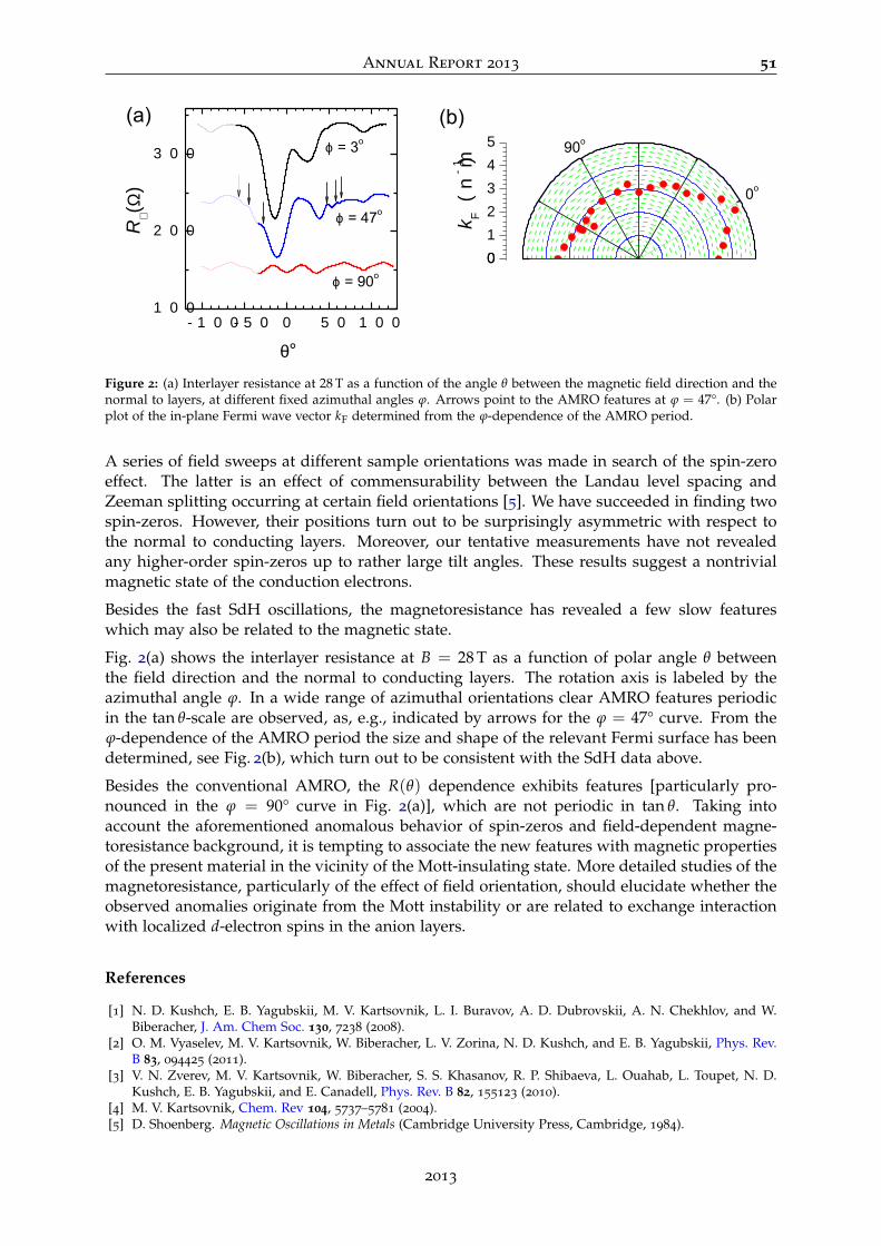
Annual Report 2013 51
012345
012345
k F (nm-1 )
- 1 0 0 - 5 0 0 5 0 1 0 01 0 0
2 0 0
3 0 0
ϕ
ϕ
R ⊥(Ω
)
θ
ϕ
Figure 2: (a) Interlayer resistance at 28 T as a function of the angle θ between the magnetic field direction and thenormal to layers, at different fixed azimuthal angles ϕ. Arrows point to the AMRO features at ϕ = 47°. (b) Polarplot of the in-plane Fermi wave vector kF determined from the ϕ-dependence of the AMRO period.
A series of field sweeps at different sample orientations was made in search of the spin-zeroeffect. The latter is an effect of commensurability between the Landau level spacing andZeeman splitting occurring at certain field orientations [5]. We have succeeded in finding twospin-zeros. However, their positions turn out to be surprisingly asymmetric with respect tothe normal to conducting layers. Moreover, our tentative measurements have not revealedany higher-order spin-zeros up to rather large tilt angles. These results suggest a nontrivialmagnetic state of the conduction electrons.
Besides the fast SdH oscillations, the magnetoresistance has revealed a few slow featureswhich may also be related to the magnetic state.
Fig. 2(a) shows the interlayer resistance at B = 28 T as a function of polar angle θ betweenthe field direction and the normal to conducting layers. The rotation axis is labeled by theazimuthal angle ϕ. In a wide range of azimuthal orientations clear AMRO features periodicin the tan θ-scale are observed, as, e.g., indicated by arrows for the ϕ = 47° curve. From theϕ-dependence of the AMRO period the size and shape of the relevant Fermi surface has beendetermined, see Fig. 2(b), which turn out to be consistent with the SdH data above.
Besides the conventional AMRO, the R(θ) dependence exhibits features [particularly pro-nounced in the ϕ = 90° curve in Fig. 2(a)], which are not periodic in tan θ. Taking intoaccount the aforementioned anomalous behavior of spin-zeros and field-dependent magne-toresistance background, it is tempting to associate the new features with magnetic propertiesof the present material in the vicinity of the Mott-insulating state. More detailed studies of themagnetoresistance, particularly of the effect of field orientation, should elucidate whether theobserved anomalies originate from the Mott instability or are related to exchange interactionwith localized d-electron spins in the anion layers.
References
[1] N. D. Kushch, E. B. Yagubskii, M. V. Kartsovnik, L. I. Buravov, A. D. Dubrovskii, A. N. Chekhlov, and W.Biberacher, J. Am. Chem Soc. 130, 7238 (2008).
[2] O. M. Vyaselev, M. V. Kartsovnik, W. Biberacher, L. V. Zorina, N. D. Kushch, and E. B. Yagubskii, Phys. Rev.B 83, 094425 (2011).
[3] V. N. Zverev, M. V. Kartsovnik, W. Biberacher, S. S. Khasanov, R. P. Shibaeva, L. Ouahab, L. Toupet, N. D.Kushch, E. B. Yagubskii, and E. Canadell, Phys. Rev. B 82, 155123 (2010).
[4] M. V. Kartsovnik, Chem. Rev 104, 5737–5781 (2004).[5] D. Shoenberg. Magnetic Oscillations in Metals (Cambridge University Press, Cambridge, 1984).
2013
52 Walther–Meißner–Institut
Low-temperature phase diagram of κ-(BETS)2FeCl4
M. Kunz, W. Biberacher, K. Neumaier, M.V. Kartsovnik 1
N.D. Kushch 2
In the last years bifunctional organic compounds showing quasi-two-dimensional metallicconduction with strong correlation effects and magnetic ordering are studied intensively. Ofspecial interest among these materials is the family (BETS)2FeX4 with X being Cl or Br. Thesecompounds can crystallize in two modifications called κ and λ differing from each other bythe structure of the molecular layer. At low temperatures all these materials show a transitioninto an antiferromagnetic (AFM) state. While λ-(BETS)2FeCl4 becomes Mott-insulating at theAFM transition, the κ compounds remain metallic. In κ-(BETS)2FeBr4 the AFM transitiontakes place at the Néel temperature TN = 2.5 K. It further shows a superconducting (SC)transition at 1.1 K. This compound was studied extensively in the past years with severalreports on the low-temperature phase diagram, see e.g. [1]. A similar behavior is reportedfor κ-(BETS)2FeCl4. It shows the transition to the AF state at TN ≈ 0.45 K and a possible SCtransition below 200 mK [2]. But up to now there exists no data on the low-temperature phasediagram. The SC transition was observed in ac-susceptibility measurements but not seen inresistance. We have performed a detailed analysis of the low temperature phase diagram ofκ-(BETS)2FeCl4 by measuring the interlayer resistance in magnetic fields down to 25 mK.
0 1 0 0 2 0 0 3 0 0 4 0 0 5 0 0 6 0 02 0
2 5
3 0
3 5
4 0
R ⊥ (m
Ω)
T ( m K )Figure 1: Temperature dependence of the interlayer re-sistance of κ-(BETS)2FeCl4 below 0.6 K.
For this experiment plate-like samples ofκ-(BETS)2FeCl4 were contacted for inter-layer magnetoresistance measurements andcooled down in a dilution refrigeratorequipped with a 2-axes vector magnet. Thesamples used showed a metallic behavior ofresistance on cooling with the resistance ra-tio R(300 K)/R(0.5 K) ≈ 5000. In Fig. 1 thetemperature dependence of the resistance forlow temperatures is plotted. The resistancedrop at ∼ 460 mK is caused by the transitioninto the AFM state. This resistance drop issupposed to be caused by reduced scatter-ing of the conduction electrons due to themagnetic ordering [2]. The sample remainsmetallic at the transition and the slope iseven increased below TN. The deviation froma linear dependence below 200 mK might be the first hint for superconductivity, however noclear SC transition was found for determination of the critical fields.
The resistance drop at the AFM transition has made it possible to track the behavior of theAFM phase boundary by just doing resistance measurements. Therefore a series of magneticfield sweeps at different constant temperatures and temperature sweeps at different constantfields were performed. This was done with magnetic field aligned parallel to each of theprincipal crystal axes. The resulting phase boundaries can be seen in Fig. 2 (note the differentscales). The filled/empty symbols represent points taken from temperature/field sweeps.
The black diamonds in Fig. 2 represent the transition for the magnetic field aligned parallel tothe b-axis (perpendicular to the conducting layers), which is the hardest axis for the AFM or-dering. The AFM state is suppressed by a magnetic field of B ≈ 1.3 T at 160 mK. Interestingly,
1This work was supported by the German Research Foundation by grant number KA 1652/4-1.2Institute of Problems of Chemical Physics, 142432 Chernogolovka, Russia
© Walther-Meißner-Institut

Annual Report 2013 53
the AFM state is apparently enhanced in small magnetic fields. At about 150 mT we find anincrease in TN by ∼ 5 mK in comparison with the zero field value.
0 . 3 0 . 4 0 . 5 0 . 6 0 . 7 0 . 8 0 . 9 1 . 0 0
2 0 0
4 0 0
6 0 0
8 0 0
1 0 0 0
1 2 0 0
1 4 0 0
B (mT
)
T / T N
0
1 0 0
2 0 0
3 0 0
4 0 0
5 0 0
6 0 0
7 0 0
B (mT
)
Figure 2: Phase diagram of κ-(BETS)2FeCl4 for different field directions. Sym-bols are explained in the text.
For a magnetic field alongthe c-axis (black triangles)the transition tempera-ture is not enhanced bythe field and already de-creases notably at 400 mT.Measurements at higherfields along this axis werenot possible due to theweak horizontal coil ofour vector magnet but areplanned for the near fu-ture.
The AFM phase bound-ary changes dramatically,if the field is applied par-allel to the a-axis, which isthe easy axis of the AFMordering, as shown by thered circles in Fig. 2. Herethe transition temperature is decreased strongly already at rather low fields and, at temper-atures below 300 mK (≈ 0.65 TN), another phase line appears. In field sweeps below thistemperature two or, in a narrow temperature interval, even three phase transitions are visi-ble. At low temperatures the system undergoes a spin-flop transition where the AFM spinorientation changes by 90°, which is supposed to be a first order phase transition. The secondAFM phase is suppressed at approximately twice the spin-flop field. Going to higher temper-atures, there exists a bicritical point at T ≈ 0.55 TN above which there is no first order phasetransition any more, but up to T ≈ 0.65 TN the spin-flopped AFM state can still be accesseddue to a reentrant transition. The phase diagram found for the fields along the a-axis looks asa textbook example for uniaxial antiferromagnets along the easy axis [3]. To the best of ourknowledge, this behavior was not reported for any other organic AFM metal including thesister compound κ-(BETS)2FeBr4 [1].
In conclusion, the AFM in κ-(BETS)2FeCl4 shows an interesting behavior in a magnetic fielapplied parallel to the different crystal axes. For fields perpendicular to the conducting layersa small enhancment of the transition temperature at low fields is observed, which, if real, hasnot be explained yet. For fields parallel to the easy axis a spin-flopped AFM phase appears,which has been theoretically predicted but, to our knowledge, not seen in experiments onorganic crystals yet.
References
[1] T. Konoike, S. Uji, T. Terashima, M. Nishimura, S. Yasuzuka, K. Enomoto, H. Fujiwara, B. Zhang, and H.Kobayashi, Phys. Rev. B 70, 094514 (2004).
[2] T. Otsuka, A. Kobayashi, Y. Miyamoto, J. Kiuchi, S. Nakamura, N. Wada, E. Fujiwara, H. Fujiwara, and H.Kobayashi, J. Solid State Chem. 159, 407–412 (2001).
[3] L. Landau, and E. Lifshitz. Electrodynamics of Continuous Media, Vol. 8 of A Course of Theoretical Physics (Perga-mon Press, 1984), 2nd edn.
2013

54 Walther–Meißner–Institut
Spin pumping in the strong coupling regime
J. Lotze, H. Huebl, M. Greifenstein, S. Geprägs, R. Gross, S. T. B. Goennenwein 1
YIG (111)GGG (111) 160 nm
Pt
7 nm
µ0HVDC
YIG epitaxial (111)
YIG single crystal50 nm
Pt
3 nm
µ0HVDC
1 mm
(a) (b)
Figure 1: (a) Sample #1: a 160 nm thick YIG film grown on a gadolin-ium gallium garnet (GGG) substrate and covered by a 7 nm thick Ptlayer. (b) Sample #2: a bulk YIG crystal covered by a YIG epilayer,followed by a thin Pt layer. In both cases, the external magnetic fieldis applied in the film plane and the DC voltage is measured perpen-dicularly to the magnetic field.
Ferromagnetic resonance (FMR) isa powerful tool for the spec-troscopy of ferromagnetic materi-als. The microwave radiation usedto excite FMR is usually enhancedby placing the sample in a reso-nant cavity. The experiments thenare carried out at fixed frequency,while sweeping the magnetic field[1]. In the interpretation of FMRmeasurements, the resonant cav-ity mode and the FMR mode ofthe magnetic sample are thought ofas separate entities, not influencingeach other. This is a valid approx-imation in the weak coupling regime, where the coupling between cavity photons andmagnons in the sample is small. However, this coupling critically depends on the amountof material in the cavity: the effective coupling between the cavity and the magnetic systemis ge f f = g0
√N, where g0 is the coupling of the cavity to a single spin, and N is the number
of spins in the sample [2]. With a sufficiently large sample, this allows us to reach the strongcoupling regime in which g2
e f f > κγ, where κ, γ are the relaxation rates of the cavity andspin system, respectively. Analogously to the the formation of a molecule from two atoms,the photonic and magnonic states then hybridize and photon-magnon superposition statesare created. This is accompanied by a characteristic anticrossing of the dispersion lines of thecavity and FMR modes, according to
ω1,2 = ωr +∆2±√
∆2 + 4g2eff , (1)
where ∆ = ωr −ωFMR = gSµB(B− BFMR)/h is the field dependent detuning [3].
Furthermore, in a ferromagnet/normal metal (FM/NM) bilayer, the resonant excitation of themagnetization creates a spin angular momentum flow – a spin current – from FM to the NMin the so-called spin pumping mechanism [4]. This enables the independent and simultaneousmeasurement of the photonic and the magnonic character of such a hybridized state in a spinpumping experiment: for the measurement of the photonic character the microwave reflectionat the cavity entrance is detected, while the magnonic character is accessible by measuring theDC voltage created by the spin current in the NM through the inverse spin Hall effect [5].
We could show that spin pumping experiments indeed are possible in both the weak and thestrong coupling regime. We simultaneously measured the FMR and spin pumping signalsof two different samples in a resonant cavity as a function of microwave frequency as wellas magnetic field: the first (sample #1) is a 160 nm thin film of ferromagnetic yttrium irongarnet (YIG), grown by pulsed laser deposition on a gadolinium gallium garnet substrateand subsequently covered with a 7 nm film of platinum (Fig.1 (a)). Since the FM layer inthis sample is thin, the coupling to the mode of the resonant cavity is expected to be small.Conversely, in sample #2, a platinum film is evaporated onto a piece of single crystal YIG with
1This work is supported by the German Research Foundation (DFG) via the project SPP 1538 "Spin CaloricTransport" and the German Excellence Initiative via the Nanosystems Initiative Munich (NIM).
© Walther-Meißner-Institut

Annual Report 2013 55
dimensions 1× 5× 1 mm3 (Fig. 1 (b)). This increase in volume of the ferromagnet is expectedto enhance the coupling by a factor of 100 relative to sample #1.
Freq
uenc
y (G
Hz)
9.86
9.85
9.84
-0.2 0.4-0.4 0 0.2Magnetic Field (T)
V DC
(µV
)
0-20-40
20
40
tYIG= 160 nm (#1)
(b)
9.86
9.85
9.84
|S11
|2
0.30.20.10
0.40.50.6(a)
Figure 2: Sample #1: (a) microwave reflection |S11|2 as a function ofmagnetic field and microwave frequency presented in a false colorplot. (b) DC voltage, measured simultaneously, in a false color plot.
The experiments were performedin a microwave cavity operating at9.848 GHz. A magnetic field of upto ±1 T was applied in the filmplane. The microwave radiationused to excite the cavity and spinsystem was provided by a vectornetwork analyzer (VNA) connectedto the cavity. The FMR was de-tected by measuring the microwavereflection S11 with the VNA. Formeasuring the spin pumping volt-age, DC leads were connected tothe sample perpendicularly to themagnetic field (Fig. 1). It wasrecorded by the auxiliary port ofthe VNA after preamplification. Inthis way it is possible to mea-sure both FMR and spin pumping
quickly and simultaneously.
In Fig. 2 (a), the microwave reflection |S11|2 is shown as a function of magnetic field andmicrowave frequency as a false color plot for sample #1. A horizontal line at the resonantfrequency of the cavity is clearly visible. The resonance frequency is in this case clearlyindependent of the applied magnetic field. This is not the case for the spin pumping voltage,also shown as a function of magnetic field and microwave frequency in Fig. 2 (b): at themagnetic field values of ±0.27 T, which are satisfying the ferromagnetic resonance condition,a spin current into the normal metal is excited resulting in a DC voltage clearly apparent asnearly vertical lines. The DC voltage changes sign with the inversion of the magnetic fielddirection as is expected from a inverse spin Hall generated voltage. This result clearly showsthe system to be in the weak coupling regime, as both the cavity and the FMR modes areessentially unperturbed, straight lines.
In contrast, Fig. 3 shows the strongly coupled case resulting from a measurement of sample#2. Panel (a) shows the microwave reflection measured as a function of microwave frequency
Freq
uenc
y (G
Hz)
09.9
10.0
9.8
9.7
-2-4-6
246
-0.2 0.4-0.9 -0.8 -0.7 -0.6 -0.5 -0.4 -0.3 -0.1 0 0.1 0.2 0.3 0.5 0.6 0.7 0.8 0.9Magnetic Field (T)
9.9
10.0
9.8
9.7
∆|S 1
1|2
-0.2-0.3-0.4-0.5
-0.10(a)
(b)
V DC
(µV
)
bulk YIG/Pt (#2)
Figure 3: Sample #2: (a) microwave reflection |S11|2 as a function of magnetic field and microwave frequencypresented in a false color plot. (b) DC voltage, measured simultaneously, in a false color plot.
2013
56 Walther–Meißner–Institut
and magnetic field as a false color plot. Around the ferromagnetic resonance conditions clearanticrossings between the dispersions of the cavity and the FMR modes can be seen, reflectingthe much stronger coupling between the cavity and the magnetic system as compared tosample #1. In addition several bulk spin wave modes are visible, which also couple to themicrowave cavity. This pattern is reproduced in Fig. 3 (b), where the measured DC voltageas a function of microwave frequency and magnetic field is shown. This voltage changessign on magnetic field inversion, as is expected for a inverse spin Hall voltage. However,the spin pumping mechanism cannot account for the DC voltages generated far away fromthe anticrossing fields, due fact that the excitation at those field values is overwhelmingly"photon-like". The DC voltage in the strong coupling limit thus appears to be much richer ascompared to the weak coupling case.
In conclusion, we have demonstrated the ability to record a spin pumping voltage at the sametime as the FMR, as a function of both magnetic field and microwave frequency. Our thinfilm sample shows the expected behavior for the weak coupling limit in both FMR and spinpumping signals. For the strongly coupled case, the FMR is shows the expected anticrossing.The DC signal follows that anticrossing, showing that spin pumping measurements in thestrong coupling regime are indeed possible.
References
[1] C. Poole. Electron Spin Resonance: A Comprehensive Treatise on Experimental Techniques/Second Edition. Doverbooks on physics (Dover Publ., 1983).
[2] D. Walls, and G. Milburn. Quantum Optics. SpringerLink: Springer e-Books (Springer, 2008).[3] H. Huebl, C. W. Zollitsch, J. Lotze, F. Hocke, M. Greifenstein, A. Marx, R. Gross, and S. T. B. Goennenwein,
Phys. Rev. Lett. 111, 127003 (2013).[4] Y. Tserkovnyak, A. Brataas, and G. E. W. Bauer, Phys. Rev. Lett. 88, 117601 (2002).[5] E. Saitoh, M. Ueda, H. Miyajima, and G. Tatara, Appl. Phys. Lett. 88, 182509 (2006).
© Walther-Meißner-Institut
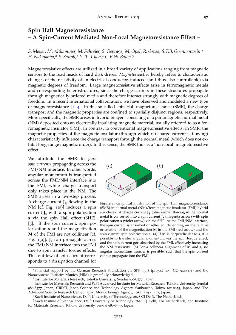
Annual Report 2013 57
Spin Hall Magnetoresistance– A Spin-Current Mediated Non-Local Magnetoresistance Effect –
S. Meyer, M. Althammer, M. Schreier, S. Geprägs, M. Opel, R. Gross, S.T.B. Goennenwein 1
H. Nakayama,2 E. Saitoh,3 Y.-T. Chen,4 G.E.W. Bauer 5
Magnetoresistive effects are utilized in a broad variety of applications ranging from magneticsensors to the read heads of hard disk drives. Magnetoresistive hereby refers to characteristicchanges of the resistivity of an electrical conductor, induced (and thus also controllable) viamagnetic degrees of freedom. Large magnetoresistive effects arise in ferromagnetic metalsand corresponding heterostructures, since the charge carriers in these structures propagatethrough magnetically ordered media and therefore interact strongly with magnetic degrees offreedom. In a recent international collaboration, we have observed and modeled a new typeof magnetoresistance [1–4]. In this so-called spin Hall magnetoresistance (SMR), the chargetransport and the magnetic properties are confined to spatially disjunct regions, respectively.More specifically, the SMR arises in hybrid bilayers consisting of a paramagnetic normal metal(NM) deposited onto an electrically insulating magnetic material, usually referred to as a fer-romagnetic insulator (FMI). In contrast to conventional magnetoresistive effects, in SMR, themagnetic properties of the magnetic insulator (through which no charge current is flowing)characteristically influence the charge transport through the normal metal (which does not ex-hibit long-range magnetic order). In this sense, the SMR thus is a ’non-local’ magnetoresistiveeffect.
JsJ
qNM
FMIM
(b)
s
JsJ
qNM
FMI
(a)M
s
Figure 1: Graphical illustration of the spin Hall magnetoresistance(SMR) in normal metal (NM)/ferromagnetic insulator (FMI) hybridstructures. A charge current Jq (blue arrow) flowing in the normalmetal is converted into a spin current Js (magenta arrow) with spinpolarization s (violet arrow) via the SHE. At the FMI/NM interface,the spin current is absorbed or reflected, depending on the relativeorientation of the magnetization M in the FMI (red arrow) and thespin current spin polarization s. (a) If M is perpendicular to s, it ispossible to transfer angular momentum via the spin torque effect,and the spin current gets absorbed by the FMI, effectively increasingthe NM resistivity. (b) For a collinear alignment of M and s, noangular momentum transfer is possible, such that the spin currentcannot propagate into the FMI.
We attribute the SMR to purespin currents propagating across theFMI/NM interface. In other words,angular momentum is transportedacross the FMI/NM interface intothe FMI, while charge transportonly takes place in the NM. TheSMR arises in a two-step process:A charge current Jq flowing in theNM [cf. Fig. 1(a)] induces a spincurrent Js with a spin polarizations via the spin Hall effect (SHE)[5]. If the spin current, spin po-larization s and the magnetizationM of the FMI are not collinear [cf.Fig. 1(a)], Js can propagate acrossthe FMI/NM interface into the FMIdue to spin transfer torque effects.This outflow of spin current corre-sponds to a dissipation channel for
1Financial support by the German Research Foundation via SPP 1538 (project no. GO 944/4-1) and theNanosystems Initiative Munich (NIM) is gratefully acknowledged.
2Institute for Materials Research, Tohoku University, Sendai 980-8577, Japan.3Institute for Materials Research and WPI Advanced Institute for Material Research, Tohoku University, Sendai
980-8577, Japan; CREST, Japan Science and Technology Agency, Sanbancho, Tokyo 102-0075, Japan, and TheAdvanced Science Research Center, Japan Atomic Energy Agency, Tokai 319 - 1195, Japan.
4Kavli Insitute of Nanoscience, Delft University of Technology, 2628 CJ Delft, The Netherlands.5Kavli Insitute of Nanoscience, Delft University of Technology, 2628 CJ Delft, The Netherlands, and Institute
for Materials Research, Tohoku University, Sendai 980-8577, Japan.
2013
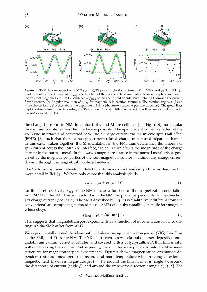
58 Walther–Meißner–Institut
-180° -90° 0° 90° 180°
406.5
406.6
406.7
ρ long
(nΩ
m)
α-90° 0° 90° 180° 270°
406.5
406.6
406.7
ρ long
(nΩ
m)
β-90° 0° 90° 180° 270°
406.5
406.6
406.7
ρ long
(nΩ
m)
γ
h||t
γ
h
j
t
n
hj
t
n
αβ
h
j
t
n
h||-th||j h||t h||-th||n h||-j h||jh||n
1 T 1 T 1 T
(a) (b) (c)
Figure 2: SMR data measured on a YIG (54 nm)/Pt (7 nm) hybrid structure at T = 300 K and µ0H = 1 T: (a)Evolution of the sheet resistivity ρlong as a function of the magnetic field orientation h for an in-plane rotation ofthe external magnetic field. (b) Dependence of ρlong on magnetic field orientation β, rotating H around the currentflow direction. (c) Angular evolution of ρlong for magnetic field rotation around t. The rotation angles α, β andγ are shown in the sketches above the experimental data (the arrows indicate positive direction). The green linesdepict a simulation of the data using the SMR model [Eq.(1)], while the dashed blue lines are a simulation withthe AMR model, Eq. (2).
the charge transport in NM. In contrast, if s and M are collinear [cf. Fig. 1(b)], no angularmomentum transfer across the interface is possible. The spin current is then reflected at theFMI/NM interface and converted back into a charge current via the inverse spin Hall effect(ISHE) [6], such that there is no spin current-related charge transport dissipation channelin this case. Taken together, the M orientation in the FMI thus determines the amount ofspin current across the FMI/NM interface, which in turn affects the magnitude of the chargecurrent in the normal metal. In this way, a magnetoresistance in the normal metal arises, gov-erned by the magnetic properties of the ferromagnetic insulator – without any charge currentflowing through the magnetically ordered material.
The SMR can be quantitatively modeled in a diffusive spin transport picture, as described inmore detail in Ref. [4]. We here only quote that this analysis yields
ρlong = ρ0 + ρ1 (m · t)2 (1)
for the sheet resistivity ρlong of the NM film, as a function of the magnetization orientationm = M/M in the FMI. The unit vector t is in the NM film plane, perpendicular to the directionj of charge current (see Fig. 2). The SMR described by Eq. (1) is qualitatively different from theconventional anisotropic magnetoresistance (AMR) of a polycrystalline, metallic ferromagnet,which obeys
ρlong = ρ0 + ∆ρ (m · j)2 . (2)
This suggests that magnetotransport experiments as a function of m orientation allow to dis-tinguish the SMR effect from AMR.
We experimentally tested the ideas outlined above, using yttrium iron garnet (YIG) thin filmsas the FMI, and Pt as the NM. The YIG films were grown via pulsed laser deposition ontogadolinium gallium garnet substrates, and covered with a polycrystalline Pt thin film in situ,without breaking the vacuum. Subsequently, the samples were patterned into Hall-bar mesastructures for magnetotransport experiments. Figure 2 shows magnetization orientation de-pendent resistance measurements, recorded at room temperature while rotating an externalmagnetic field H with a magnitude µ0H = 1 T around the film normal n (angle α), aroundthe direction j of current (angle β), and around the transverse direction t (angle γ) [3, 7]. The
© Walther-Meißner-Institut

Annual Report 2013 59
green lines in Fig. 2 depict the magnetoresistance expected for SMR according to Eq. (1), whilethe dashed blue lines show the behavior expected for AMR, Eq. (2). Clearly, our experimentaldata is in excellent qualitative as well as quantitative agreement with the SMR theory, whileconventional AMR cannot explain the observed magnetoresistance. In particular, we thuscan exclude magnetoresistive effects in a spin-polarized metallic layer in Pt, induced at theYIG/Pt interface due to the magnetic proximity effect [8], as the origin of the magnetoresis-tance in our YIG/Pt samples. This notion is further corroborated by X-ray magnetic circulardichroism measurements [9]. Let us also mention that the excellent agreement between SMRtheory and experiment is not limited to the sheet resistivity ρlong. Rather, the SMR modelalso quantitatively accounts for the transverse magnetoresistance (misleadingly often calledplanar Hall effect in the literature), as well as the anomalous Hall-effect type magnetogalvanicvoltages observed in our YIG/Pt hybrids. We furthermore could show that the SMR existsnot only in YIG/Pt hybrids, but also in YIG/Au/Pt, YIG/Cu/Pt, Fe3O4/Pt, and NiFe2O4/Ptheterostructures [3]. These results establish the SMR as a universal and robust effect, givingstraightforward access to spin transport parameters such as the spin diffusion length and thespin Hall angle in the normal metal. Moreover, the SMR effect is quantitatively consistentwith other spin-current related phenomena, in particular spin pumping and the spin Seebeckeffect, as discussed in more detail in Ref. [10].
In summary, we have experimentally observed and theoretically modeled a novel magnetore-sistance effect, which is based on pure spin current flow across a FMI/NM interface. Thisso-called spin Hall magnetoresistance is determined by the transmission viz. the reflection ofa pure spin current at a FMI/NM interface, depending on the orientation of the magnetiza-tion in the magnetic insulator with respect to the spin current spin polarization in the normalmetal. Although no charge current can penetrate into the magnetic insulator, its magneticproperties nevertheless characteristically impact the charge transport in the adjacent normalmetal. SMR experiments allow to quantify the spin transport parameters in the normal metal,and provide important complementary information for spin caloritronics experiments in fer-romagnet/normal metal hybrid structures.
References
[1] M. Weiler, M. Althammer, F. D. Czeschka, H. Huebl, M. S. Wagner, M. Opel, I. Imort, G. Reiss, A. Thomas,R. Gross, and S. T. B. Goennenwein, Phys. Rev. Lett. 108, 106602 (2012).
[2] H. Nakayama, M. Althammer, Y.-T. Chen, K. Uchida, Y. Kajiwara, D. Kikuchi, T. Ohtani, S. Geprägs, M.Opel, S. Takahashi, R. Gross, G. E. W. Bauer, S. T. B. Goennenwein, and E. Saitoh, Phys. Rev. Lett. 110,206601 (2013).
[3] M. Althammer, S. Meyer, H. Nakayama, M. Schreier, S. Altmannshofer, M. Weiler, H. Huebl, S. Geprägs, M.Opel, R. Gross, D. Meier, C. Klewe, T. Kuschel, J.-M. Schmalhorst, G. Reiss, L. Shen, A. Gupta, Y.-T. Chen,G. E. W. Bauer, E. Saitoh, and S. T. B. Goennenwein, Phys. Rev. B 87, 224401 (2013).
[4] Y.-T. Chen, S. Takahashi, H. Nakayama, M. Althammer, S. T. B. Goennenwein, E. Saitoh, and G. E. W. Bauer,Phys. Rev. B 87, 144411 (2013).
[5] J. E. Hirsch, Phys. Rev. Lett. 83, 1834–1837 (1999).[6] E. Saitoh, M. Ueda, H. Miyajima, and G. Tatara, Appl. Phys. Lett. 88, 182509 (2006).[7] W. Limmer, M. Glunk, J. Daeubler, T. Hummel, W. Schoch, R. Sauer, C. Bihler, H. Huebl, M. S. Brandt, and
S. T. B. Goennenwein, Phys. Rev. B 74, 205205 (2006).[8] Y. M. Lu, Y. Choi, C. M. Ortega, X. M. Cheng, J. W. Cai, S. Y. Huang, L. Sun, and C. L. Chien, Phys. Rev. Lett.
110, 147207 (2013).[9] S. Geprägs, S. Meyer, S. Altmannshofer, M. Opel, F. Wilhelm, A. Rogalev, R. Gross, and S. T. B. Goennenwein,
Appl. Phys. Lett. 101, 262407 (2012).[10] M. Weiler, M. Althammer, M. Schreier, J. Lotze, M. Pernpeintner, S. Meyer, H. Huebl, R. Gross, A. Kamra, J.
Xiao, Y.-T. Chen, H. Jiao, G. E. W. Bauer, and S. T. B. Goennenwein, Phys. Rev. Lett. 111, 176601 (2013).
2013

60 Walther–Meißner–Institut
Magnon, phonon and electron temperature profiles and the spin See-beck effect in magnetic insulator/normal metal hybrid structures
M. Schreier, M. Weiler, S. Meyer, M. Althammer, M. Opel, S. Geprägs, R. Gross,S. T. B. Goennenwein 1
A. Kamra2, J. Xiao3,4, G. E. W. Bauer5,6
Figure 1: In the (longitudinal) spin Seebeck effect a differ-ence ∆Tme between the temperature Tm of the magnonsin a ferromagnet (FM) and the temperature Te of the elec-trons in a normal metal (NM) causes a spin current js be-tween the ferromagnet and the normal metal that is con-verted into a charge current jjjc ∝ jsxxx × sss by the inversespin Hall effect, where sss = −MMM/|MMM| is the polarizationvector of the spin current and MMM is the magnetizationvector.
The spin Seebeck effect [1, 2] (SSE) allows togenerate pure spin currents from thermal ex-citations. While the spin Seebeck effect itselfhas been experimentally established [1–9],an agreement between experiments and the-ory [10, 11] has proven elusive. In experi-mental publications the average temperaturegradient across the entire sample is usuallyquoted, while the thermodynamic state (lo-cal temperature profile) at the interface atwhich the spin current is generated, couldnot be measured yet. According to the spinSeebeck theory, however, the knowledge ofthe actual temperature difference ∆Tme betweenthe magnon and the electron systems at theferromagnet/normal metal interface is cru-cial, since ∆Tme determines the magnitudeof the spin current [10]. The temperaturedifference ∆Tme arises due to different ther-mal properties and boundary conditions forthe magnons, phonons and electrons in theferromagnet/normal metal hybrids used inexperiments. The phonon (Tp), electron (Te)and magnon (Tm) temperature profiles in asubstrate/ferromagnet/normal metal multi-layer structure are schematically depicted inFig. 1. As detailed in this report, the temper-ature profiles can show discontinuities at the material interfaces due to interface propertiessuch as the Kapitza resistance [12]. Temperature profiles are not easily measurable for a non-equilibrium situation in which magnon, phonon, and electron temperatures differ. To date,an in depth analysis and interpretation of experimental spin Seebeck effect data is possibleonly by modeling the magnon, phonon, and electron temperature profiles based on the rele-vant material parameters. Especially for magnetic insulators the determination of the phonontemperature Tp profile is of central importance in this approach [13, 14].
1Financial support from the German Research Foundation via SPP 1538 “Spin Caloric Transport”, Project No.GO 944/4-1, and the German Excellence Initiative via the Nanosystems Initiative Munich (NIM) is gratefullyacknowledged.
2Kavli Institute of Nanoscience, Delft University of Technology, Delft, The Netherlands.3Department of Physics and State Key Laboratory of Surface Physics, Fudan University, Shanghai, China.4Supported by the National Natural Science Foundation of China (No. 11004036, No. 91121002).5Kavli Institute of Nanoscience, Delft University of Technology, Delft, The Netherlands
Institute for Materials Research and WPI-AIMR, Tohoku University, Sendai, Japan.6Supported by the German Research Foundation via SPP 1538 “Spin Caloric Transport”, Project No. GO
944/4-1 and BA 2954/1-1, FOM (Stichting voor Fundamenteel Onderzoek der Materie), EU-ICT-7 “MACALO”,the ICC-IMR, Grand-in-Aid for Scientific Research (Kakenhi) A 25247056.
© Walther-Meißner-Institut

Annual Report 2013 61
1 0 - 4 1 0 - 5 1 0 - 6 1 0 - 7 1 0 - 8 1 0 - 93 0 0
3 1 0
3 2 0
3 3 0
3 4 0
Temp
eratur
e (K)
( m )
p e m
P tY I GG G G
8 0 7 0 6 0 5 0 4 0 3 0 2 0 1 0 03 3 2
3 3 4
3 3 6
3 3 8
Temp
eratur
e (K)
( n m )
Figure 2: Phonon, electron and magnon temperature distributionsalong the optical axis of the laser beam at 10 mW laser power in aGGG(500 µm)/YIG(54 nm)/Pt(7 nm) sample calculated via 3D FEMfor the entire sample. The inset shows the thin film region.
We have modeled and calcu-lated the phonon, electron andmagnon temperature profiles inferromagnet/normal metal hybridstructures, by solving the heattransport equations with appro-priate boundary conditions utiliz-ing three-dimensional finite ele-ment (3D FEM) solvers (COM-SOL7). Details can be found inRef. [15]. In particular, we explic-itly take into account the heat cur-rent carried by the pumped spincurrent through the interface. Forthe sake of simplicity, we here limitthe discussion to hybrids based onthe ferrimagnetic insulator yttriumiron garnet (Y3Fe5O12, YIG). Themagnon temperature calculationsare based on the work by Sanders and Walton [14] and Xiao et al. [10], that we extensivelyuse with a focus on ultrathin films in which interfacial effects become important for the ther-mal transport. The Tp, Te, and Tm profiles thus obtained yield the temperature difference∆Tme at the magnetic insulator/normal metal interfaces, from which the spin Seebeck volt-age can be inferred [10]. The voltages thus calculated agree well with our spatially resolvedlongitudinal spin Seebeck effect measurements [6, 15].
0 5 1 0 1 5 2 0 2 50
2 5
5 0
7 5
1 0 0
1 2 5
S S E E x p e r i m e n t S S E S i m u l a t i o n
SS
E(La
ser =
1 mW
) (nV)
P t ( n m )Figure 3: Comparison of the observed and computed spin Seebeckvoltages under local laser heating. The open circles depict the samplewith an additional gold layer between the platinum and the YIG. Agood agreement between theory and experiment is found.
Figure 2 shows the phonon, elec-tron, and magnon temperature pro-files induced by local laser illu-mination (laser heating) [6] alongthe film normal x. The phonontemperature (blue line) shows pro-nounced jumps at the interfaces be-tween the individual layer, stem-ming from interfacial thermal re-sistances. This also affects elec-tron and magnon temperature dueto their strong coupling with thephonons. Thereby, the inclusionof interfacial thermal resistanceleads to a substantial increase in∆Tme by about an order of mag-nitude. Nevertheless, we find thatthe coupling between electrons andmagnons across the YIG/Pt inter-face is strong enough as to almosteliminate ∆Tme which is of the order of only a few millikelvins. The strong interaction be-tween electrons and magnons is caused by the energy (heat) transport associated with thespin current, leading to the spin Seebeck effect.
Figure 3 shows a comparison between the voltages measured experimentally in our local
7COMSOL Multiphysics®4.3a
2013
62 Walther–Meißner–Institut
laser heating setup [6, 16] and theoretical values obtained from our simulations for differentYIG/Pt heterostructures of varying layer thicknesses. For a YIG(54 nm)/Pt(7 nm) sample,for example, a voltage VSSE = 74 nV is observed in experiment for Plaser = 1 mW at thesample surface. This compares reasonably well to the VSSE = 37 nV that we obtain from oursimulation. This agreement is not limited to this particular sample as can be seen in Fig. 3.Generally the calculated ∆Tme seem to be somewhat underestimated, possibly owing to themagnon property parameters used [15].
In summary, our detailed temperature profile calculations together with the spin Seebeckeffect theory [10] allow us to quantitatively reproduce the spin Seebeck voltages observed inour experiments. Our model calculations in particular show that thermal coupling betweenthe magnons in the ferromagnet and the electrons in the normal metal notably affects themagnon temperature in the ferromagnet, an issue widely neglected in the literature so far.
References
[1] K. Uchida, S. Takahashi, K. Harii, J. Ieda, W. Koshibae, K. Ando, S. Maekawa, and E. Saitoh, Nature 455,778–781 (2008).
[2] K. Uchida, H. Adachi, T. Ota, H. Nakayama, S. Maekawa, and E. Saitoh, Appl. Phys. Lett. 97, 172505 (2010).[3] K. Uchida, J. Xiao, H. Adachi, J. Ohe, S. Takahashi, J. Ieda, T. Ota, Y. Kajiwara, H. Umezawa, H. Kawai,
G. E. W. Bauer, S. Maekawa, and E. Saitoh, Nat. Mater. 9, 894–897 (2010).[4] K. Uchida, T. Nonaka, T. Ota, and E. Saitoh, Applied Physics Letters 97, 262504 (2010).[5] C. M. Jaworski, J. Yang, S. Mack, D. D. Awschalom, J. P. Heremans, and R. C. Myers, Nat. Mater. 9, 898–903
(2010).[6] M. Weiler, M. Althammer, F. D. Czeschka, H. Huebl, M. S. Wagner, M. Opel, I.-M. Imort, G. Reiss, A. Thomas,
R. Gross, and S. T. B. Goennenwein, Phys. Rev. Lett. 108, 106602 (2012).[7] D. Meier, T. Kuschel, L. Shen, A. Gupta, T. Kikkawa, K. Uchida, E. Saitoh, J.-M. Schmalhorst, and G. Reiss,
Phys. Rev. B 87, 054421 (2013).[8] D. Qu, S. Y. Huang, J. Hu, R. Wu, and C. L. Chien, Phys. Rev. Lett. 110, 067206 (2013).[9] T. Kikkawa, K. Uchida, Y. Shiomi, Z. Qiu, D. Hou, D. Tian, H. Nakayama, X.-F. Jin, and E. Saitoh, Phys. Rev.
Lett. 110, 067207 (2013).[10] J. Xiao, G. E. W. Bauer, K. Uchida, E. Saitoh, and S. Maekawa, Phys. Rev. B 81, 214418 (2010).[11] H. Adachi, J.-i. Ohe, S. Takahashi, and S. Maekawa, Phys. Rev. B 83, 094410 (2011).[12] P. L. Kapitza, Journal of Physics 4, 181–210 (1941).[13] M. I. Kaganov, I. M. Lifshitz, and L. V. Tanatarov, Sov. Phys. JETP 4, 173–178 (1957).[14] D. J. Sanders, and D. Walton, Phys. Rev. B 15, 1489–1494 (1977).[15] M. Schreier, A. Kamra, M. Weiler, J. Xiao, G. E. W. Bauer, R. Gross, and S. T. B. Goennenwein, Phys. Rev. B
88, 094410 (2013).[16] M. Schreier. Spatially resolved spin Seebeck experiments. Master’s thesis, Technische Universität München
(2012).
© Walther-Meißner-Institut

Application–Oriented Research
63

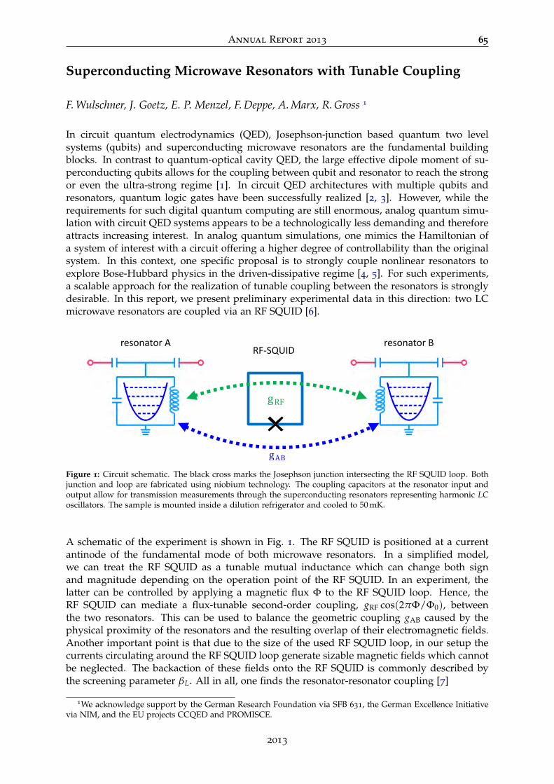
Annual Report 2013 65
Superconducting Microwave Resonators with Tunable Coupling
F. Wulschner, J. Goetz, E. P. Menzel, F. Deppe, A. Marx, R. Gross 1
In circuit quantum electrodynamics (QED), Josephson-junction based quantum two levelsystems (qubits) and superconducting microwave resonators are the fundamental buildingblocks. In contrast to quantum-optical cavity QED, the large effective dipole moment of su-perconducting qubits allows for the coupling between qubit and resonator to reach the strongor even the ultra-strong regime [1]. In circuit QED architectures with multiple qubits andresonators, quantum logic gates have been successfully realized [2, 3]. However, while therequirements for such digital quantum computing are still enormous, analog quantum simu-lation with circuit QED systems appears to be a technologically less demanding and thereforeattracts increasing interest. In analog quantum simulations, one mimics the Hamiltonian ofa system of interest with a circuit offering a higher degree of controllability than the originalsystem. In this context, one specific proposal is to strongly couple nonlinear resonators toexplore Bose-Hubbard physics in the driven-dissipative regime [4, 5]. For such experiments,a scalable approach for the realization of tunable coupling between the resonators is stronglydesirable. In this report, we present preliminary experimental data in this direction: two LCmicrowave resonators are coupled via an RF SQUID [6].
RF-SQUID
gRF
gAB
resonator A resonator B
Figure 1: Circuit schematic. The black cross marks the Josephson junction intersecting the RF SQUID loop. Bothjunction and loop are fabricated using niobium technology. The coupling capacitors at the resonator input andoutput allow for transmission measurements through the superconducting resonators representing harmonic LCoscillators. The sample is mounted inside a dilution refrigerator and cooled to 50 mK.
A schematic of the experiment is shown in Fig. 1. The RF SQUID is positioned at a currentantinode of the fundamental mode of both microwave resonators. In a simplified model,we can treat the RF SQUID as a tunable mutual inductance which can change both signand magnitude depending on the operation point of the RF SQUID. In an experiment, thelatter can be controlled by applying a magnetic flux Φ to the RF SQUID loop. Hence, theRF SQUID can mediate a flux-tunable second-order coupling, gRF cos(2πΦ/Φ0), betweenthe two resonators. This can be used to balance the geometric coupling gAB caused by thephysical proximity of the resonators and the resulting overlap of their electromagnetic fields.Another important point is that due to the size of the used RF SQUID loop, in our setup thecurrents circulating around the RF SQUID loop generate sizable magnetic fields which cannotbe neglected. The backaction of these fields onto the RF SQUID is commonly described bythe screening parameter βL. All in all, one finds the resonator-resonator coupling [7]
1We acknowledge support by the German Research Foundation via SFB 631, the German Excellence Initiativevia NIM, and the EU projects CCQED and PROMISCE.
2013

66 Walther–Meißner–Institut
g = gAB + gRFcos(2πΦ/Φ0)
1 + βL cos(2πΦ/Φ0)(1)
flux (mΦ0)
frequ
ency
(GH
z)
−800 −600 −400 −2006.3
6.35
6.4
6.45
6.5
6.55
6.6
6.65
6.7
−135
−130
−125
−120
−115
−110
−105
−100
−95
−90
trans
mis
sion
mag
nitu
de (d
B)
Figure 2: Transmission magnitude (color code) as a function of prob-ing frequency and applied flux through the RF SQUID loop.
For βL > 1, the RF SQUIDhas multiple metastable operationpoints, which is undesirable fora well-controlled coupling mecha-nism. However, a small βL re-duces gRF because it implies a smallloop size and/or a small criticalcurrent of the RF SQUID junc-tion. Therefore, we choose βLsmaller than, but close to unity.We can clearly see the tunable cou-pling in the transmission measure-ment through one of the resonatorsshown in Fig. 2. In particular, thespacing between the two normalmodes is reduced near half a fluxquantum in the RF SQUID loop. Asthe next step, we plan to optimizethe circuit parameters such that wecan completely decouple the res-onators. Such an improved devicehas potential applications in analogquantum simulations and quantuminformation processing with prop-agating microwave photons. A fur-ther interesting aspect is to drive the coupling at a high frequency. This should allow for theobservation of squeezing and parametric amplification as proposed in Ref. [8].
References
[1] T. Niemczyk, F. Deppe, H. Huebl, E. P. Menzel, F. Hocke, M. J. Schwarz, J. J. Garcia-Ripoll, D. Zueco, T.Huemmer, E. Solano, A. Marx, and R. Gross, Nature Phys. 6, 772–776 (2010).
[2] E. Lucero, R. Barends, Y. Chen, J. Kelly, M. Mariantoni, A. Megrant, P. O. Malley, D. Sank, A. Vainsencher, J.Wenner, T. White, Y. Yin, A. N. Cleland, and J. M. Martinis, Nature Phys. 8, 719–723 (2012).
[3] A. Fedorov, L. Steffen, M. Baur, M. P. da Silva, and A. Wallraff, Nature 481, 170–172 (2011).[4] M. Leib, and M. J. Hartmann, New J. of Phys. 12, 093031 (2010).[5] M. Leib, F. Deppe, A. Marx, R. Gross, and M. J. Hartmann, New. J. of Phys. 14, 075024 (2012).[6] B. Peropadre, D. Zueco, F. Wulschner, F. Deppe, A. Marx, R. Gross, and J. Garcia-Ripoll, Phys. Rev. B 87,
134504 (2013).[7] M. S. Allman, F. Altomare, J. D. Whittaker, K. Cicak, D. Li, A. Sirois, J. Strong, J. D. Teufel, and R. W.
Simmonds, Phys. Rev. Lett. 104, 177004 (2010).[8] L. Tian, M. S. Allman, and R. W. Simmonds, New J. of Phys. 10, 115001 (2008).
© Walther-Meißner-Institut
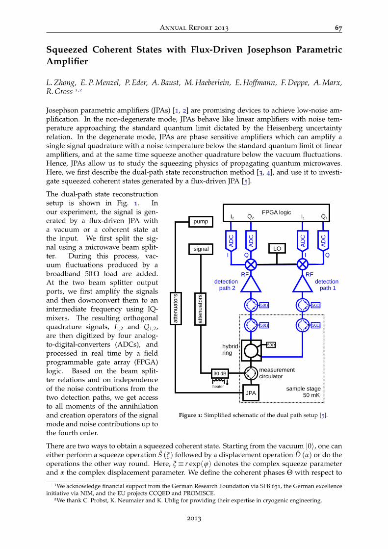
Annual Report 2013 67
Squeezed Coherent States with Flux-Driven Josephson ParametricAmplifier
L. Zhong, E. P. Menzel, P. Eder, A. Baust, M. Haeberlein, E. Hoffmann, F. Deppe, A. Marx,R. Gross 1,2
Josephson parametric amplifiers (JPAs) [1, 2] are promising devices to achieve low-noise am-plification. In the non-degenerate mode, JPAs behave like linear amplifiers with noise tem-perature approaching the standard quantum limit dictated by the Heisenberg uncertaintyrelation. In the degenerate mode, JPAs are phase sensitive amplifiers which can amplify asingle signal quadrature with a noise temperature below the standard quantum limit of linearamplifiers, and at the same time squeeze another quadrature below the vacuum fluctuations.Hence, JPAs allow us to study the squeezing physics of propagating quantum microwaves.Here, we first describe the dual-path state reconstruction method [3, 4], and use it to investi-gate squeezed coherent states generated by a flux-driven JPA [5].
50Ω
50Ω
50Ω 50Ω
50Ω
LOAD
C
AD
C
ADC
AD
C
FPGA logic
JPA
pump
signal
atte
nuat
ors
30 dB
heater
atte
nuat
ors
sample stage 50 mK
hybridring
detection path 2
RFRF
I
I2 Q2 I1 Q1
Q I Q
detection path 1
measurementcirculator
Figure 1: Simplified schematic of the dual path setup [5].
The dual-path state reconstructionsetup is shown in Fig. 1. Inour experiment, the signal is gen-erated by a flux-driven JPA witha vacuum or a coherent state atthe input. We first split the sig-nal using a microwave beam split-ter. During this process, vac-uum fluctuations produced by abroadband 50 Ω load are added.At the two beam splitter outputports, we first amplify the signalsand then downconvert them to anintermediate frequency using IQ-mixers. The resulting orthogonalquadrature signals, I1,2 and Q1,2,are then digitized by four analog-to-digital-converters (ADCs), andprocessed in real time by a fieldprogrammable gate array (FPGA)logic. Based on the beam split-ter relations and on independenceof the noise contributions from thetwo detection paths, we get accessto all moments of the annihilationand creation operators of the signalmode and noise contributions up tothe fourth order.
There are two ways to obtain a squeezed coherent state. Starting from the vacuum |0〉, one caneither perform a squeeze operation S (ξ) followed by a displacement operation D (α) or do theoperations the other way round. Here, ξ≡ r exp(ϕ) denotes the complex squeeze parameterand α the complex displacement parameter. We define the coherent phases Θ with respect to
1We acknowledge financial support from the German Research Foundation via SFB 631, the German excellenceinitiative via NIM, and the EU projects CCQED and PROMISCE.
2We thank C. Probst, K. Neumaier and K. Uhlig for providing their expertise in cryogenic engineering.
2013
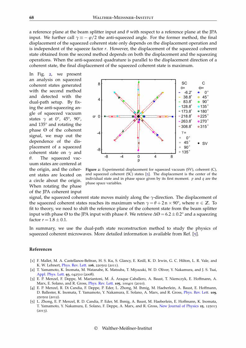
68 Walther–Meißner–Institut
a reference plane at the beam splitter input and θ with respect to a reference plane at the JPAinput. We further call γ≡− ϕ/2 the anti-squeezed angle. For the former method, the finaldisplacement of the squeezed coherent state only depends on the displacement operation andis independent of the squeeze factor r. However, the displacement of the squeezed coherentstate obtained from the second method depends on both the displacement and the squeezingoperations. When the anti-squeezed quadrature is parallel to the displacement direction of acoherent state, the final displacement of the squeezed coherent state is maximum.
-8 -4 0 4 8p
-8
-4
0
4
8
q
SCθ=
83.8o
38.8o
-6.2o
308.8o
263.8o
218.8o
173.8o
128.8o
SV
CΘ=
90o
45o
0 o
315o
270o
225o
180o
135o
γ=
90o
45o
0 o
135o
Figure 2: Experimental displacement for squeezed vacuum (SV), coherent (C),and squeezed coherent (SC) states [5]. The displacement is the center of theindividual state and in phase space given by its first moment. p and q are thephase space variables.
In Fig. 2, we presentan analysis on squeezedcoherent states generatedwith the second methodand detected with thedual-path setup. By fix-ing the anti-squeezing an-gle of squeezed vacuumstates γ at 0°, 45°, 90°,and 135° and rotating thephase Θ of the coherentsignal, we map out thedependence of the dis-placement of a squeezedcoherent state on γ andθ. The squeezed vac-uum states are centered atthe origin, and the coher-ent states are located ona circle about the origin.When rotating the phaseof the JPA coherent inputsignal, the squeezed coherent state moves mainly along the γ-direction. The displacement ofthe squeezed coherent states reaches its maximum when γ= θ + 2 n× 90°, where n ∈ Z. Tofit to theory, we need to shift the reference plane of the coherent state from the beam splitterinput with phase Θ to the JPA input with phase θ. We retrieve ∆Θ= 6.2± 0.2° and a squeezingfactor r = 1.8± 0.1.
In summary, we use the dual-path state reconstruction method to study the physics ofsqueezed coherent microwaves. More detailed information is available from Ref. [5].
References
[1] F. Mallet, M. A. Castellanos-Beltran, H. S. Ku, S. Glancy, E. Knill, K. D. Irwin, G. C. Hilton, L. R. Vale, andK. W. Lehnert, Phys. Rev. Lett. 106, 220502 (2011).
[2] T. Yamamoto, K. Inomata, M. Watanabe, K. Matsuba, T. Miyazaki, W. D. Oliver, Y. Nakamura, and J. S. Tsai,Appl. Phys. Lett. 93, 042510 (2008).
[3] E. P. Menzel, F. Deppe, M. Mariantoni, M. Á. Araque Caballero, A. Baust, T. Niemczyk, E. Hoffmann, A.Marx, E. Solano, and R. Gross, Phys. Rev. Lett. 105, 100401 (2010).
[4] E. P. Menzel, R. Di Candia, F. Deppe, P. Eder, L. Zhong, M. Ihmig, M. Haeberlein, A. Baust, E. Hoffmann,D. Ballester, K. Inomata, T. Yamamoto, Y. Nakamura, E. Solano, A. Marx, and R. Gross, Phys. Rev. Lett. 109,250502 (2012).
[5] L. Zhong, E. P. Menzel, R. D. Candia, P. Eder, M. Ihmig, A. Baust, M. Haeberlein, E. Hoffmann, K. Inomata,T. Yamamoto, Y. Nakamura, E. Solano, F. Deppe, A. Marx, and R. Gross, New Journal of Physics 15, 125013
(2013).
© Walther-Meißner-Institut
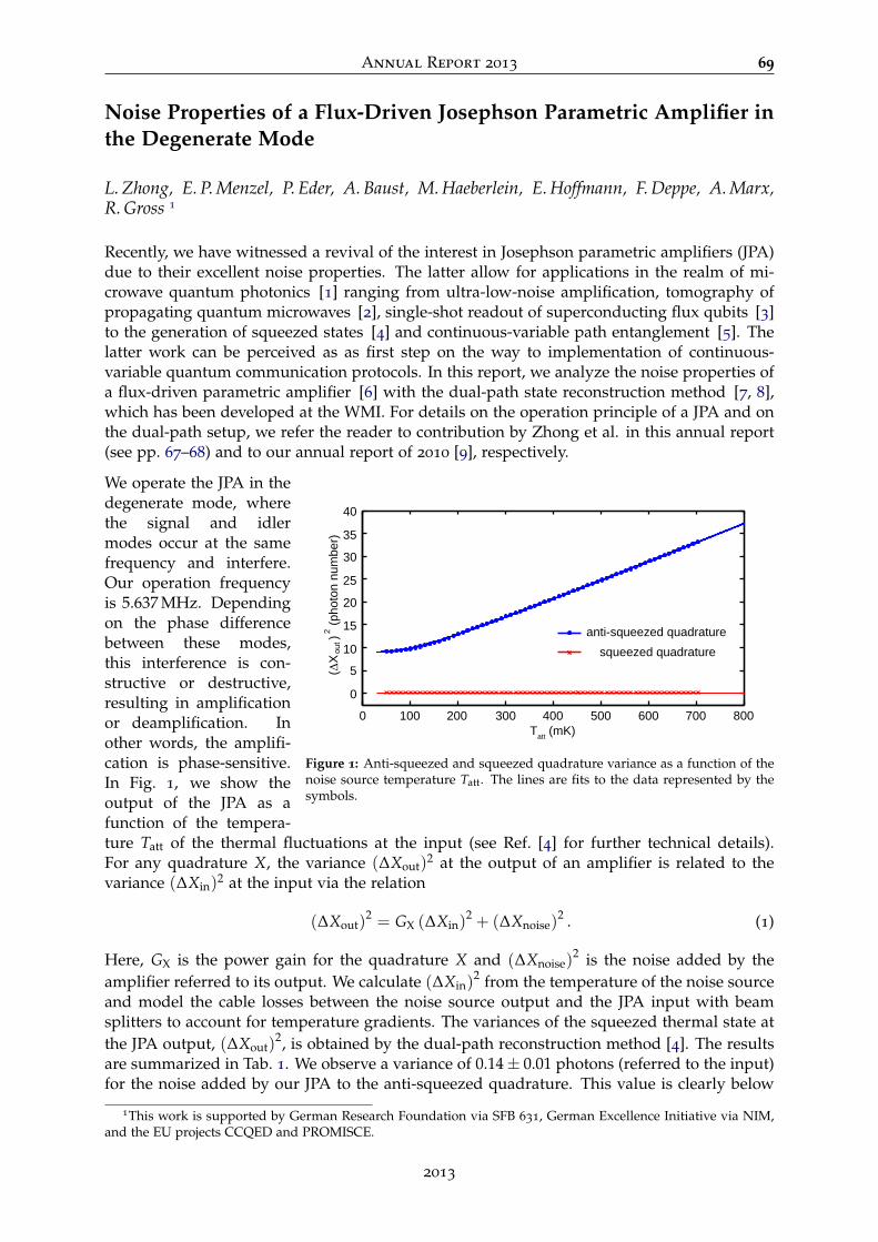
Annual Report 2013 69
Noise Properties of a Flux-Driven Josephson Parametric Amplifier inthe Degenerate Mode
L. Zhong, E. P. Menzel, P. Eder, A. Baust, M. Haeberlein, E. Hoffmann, F. Deppe, A. Marx,R. Gross 1
Recently, we have witnessed a revival of the interest in Josephson parametric amplifiers (JPA)due to their excellent noise properties. The latter allow for applications in the realm of mi-crowave quantum photonics [1] ranging from ultra-low-noise amplification, tomography ofpropagating quantum microwaves [2], single-shot readout of superconducting flux qubits [3]to the generation of squeezed states [4] and continuous-variable path entanglement [5]. Thelatter work can be perceived as as first step on the way to implementation of continuous-variable quantum communication protocols. In this report, we analyze the noise properties ofa flux-driven parametric amplifier [6] with the dual-path state reconstruction method [7, 8],which has been developed at the WMI. For details on the operation principle of a JPA and onthe dual-path setup, we refer the reader to contribution by Zhong et al. in this annual report(see pp. 67–68) and to our annual report of 2010 [9], respectively.
squeezed quadratureanti-squeezed quadrature
0 100 200 300 400 500 600 700 800
0
5
10
15
20
25
30
35
40
Tatt (mK)
(ΔX
out
) (
phot
on n
umbe
r)
2
Figure 1: Anti-squeezed and squeezed quadrature variance as a function of thenoise source temperature Tatt. The lines are fits to the data represented by thesymbols.
We operate the JPA in thedegenerate mode, wherethe signal and idlermodes occur at the samefrequency and interfere.Our operation frequencyis 5.637 MHz. Dependingon the phase differencebetween these modes,this interference is con-structive or destructive,resulting in amplificationor deamplification. Inother words, the amplifi-cation is phase-sensitive.In Fig. 1, we show theoutput of the JPA as afunction of the tempera-ture Tatt of the thermal fluctuations at the input (see Ref. [4] for further technical details).For any quadrature X, the variance (∆Xout)2 at the output of an amplifier is related to thevariance (∆Xin)2 at the input via the relation
(∆Xout)2 = GX (∆Xin)
2 + (∆Xnoise)2 . (1)
Here, GX is the power gain for the quadrature X and (∆Xnoise)2 is the noise added by the
amplifier referred to its output. We calculate (∆Xin)2 from the temperature of the noise source
and model the cable losses between the noise source output and the JPA input with beamsplitters to account for temperature gradients. The variances of the squeezed thermal state atthe JPA output, (∆Xout)
2, is obtained by the dual-path reconstruction method [4]. The resultsare summarized in Tab. 1. We observe a variance of 0.14± 0.01 photons (referred to the input)for the noise added by our JPA to the anti-squeezed quadrature. This value is clearly below
1This work is supported by German Research Foundation via SFB 631, German Excellence Initiative via NIM,and the EU projects CCQED and PROMISCE.
2013

70 Walther–Meißner–Institut
Table 1: Results of the dual-path analysis of the JPA gain and the noise along the squeezed (sq) and anti-squeezed(anti) quadratures. The error bars describe the statistical error obtained from the fitting procedure. (∆Xnoise)
2 isgiven in units of photon number.
X GX (dB) (∆Xnoise)2 (∆Xnoise)
2 /GXsq −11.7± 0.3 0.06± 0.01 –anti 13.7± 0.1 – 0.14± 0.01
the standard quantum limit for a single quadrature of a phase-insensitive amplifier, whichis 0.25 photons for our quadrature definition. The relevant noise number for the use of theJPA as a squeezer is the noise it adds to the squeezed quadrature at the JPA output, which is0.06 photons.
In summary, we have verified that our JPA, when operated as a phase-sensitive device, addsless noise to the amplified quadrature than an ideal phase-insensitive amplifier. This propertyis of utmost importance for high efficiency photon detection, state tomography and quantumcommunication applications in the microwave domain.
References
[1] Y. Nakamura, and T. Yamamoto, IEEE Photon. J. 5, 0701406 (2013).[2] F. Mallet, M. A. Castellanos-Beltran, H. S. Ku, S. Glancy, E. Knill, K. D. Irwin, G. C. Hilton, L. R. Vale, and
K. W. Lehnert, Phys. Rev. Lett. 106, 220502 (2011).[3] Z. R. Lin, K. Inomata, W. D. Oliver, K. Koshino, Y. Nakamura, J. S. Tsai, and T. Yamamoto, Appl. Phys. Lett.
103, 132602 (2013).[4] L. Zhong, E. P. Menzel, R. D. Candia, P. Eder, M. Ihmig, A. Baust, M. Haeberlein, E. Hoffmann, K. Inomata,
T. Yamamoto, Y. Nakamura, E. Solano, F. Deppe, A. Marx, and R. Gross, New Journal of Physics 15, 125013
(2013).[5] E. P. Menzel, R. Di Candia, F. Deppe, P. Eder, L. Zhong, M. Ihmig, M. Haeberlein, A. Baust, E. Hoffmann,
D. Ballester, K. Inomata, T. Yamamoto, Y. Nakamura, E. Solano, A. Marx, and R. Gross, Phys. Rev. Lett. 109,250502 (2012).
[6] T. Yamamoto, K. Inomata, M. Watanabe, K. Matsuba, T. Miyazaki, W. D. Oliver, Y. Nakamura, and J. S. Tsai,Appl. Phys. Lett. 93, 042510 (2008).
[7] E. P. Menzel, F. Deppe, M. Mariantoni, M. Á. Araque Caballero, A. Baust, T. Niemczyk, E. Hoffmann, A.Marx, E. Solano, and R. Gross, Phys. Rev. Lett. 105, 100401 (2010).
[8] R. Di Candia, E. P. Menzel, L. Zhong, F. Deppe, A. Marx, R. Gross, and E. Solano. Dual-Path Methods forPropagating Quantum Microwaves. Accepted for publication in New J. of Phys., arXiv:1308.3117 (2013).
[9] A. Baust, E. P. Menzel, T. Niemczyk, E. Hoffmann, M. Häberlein, F. Deppe, A. Marx, R. Gross, K. Inomata,T. Yamamoto, and Y. Nakamura. Characterization of a Flux-Driven Josephson Parametric Amplifier. In WMIAnnual Report, 34–35 (2010).
© Walther-Meißner-Institut
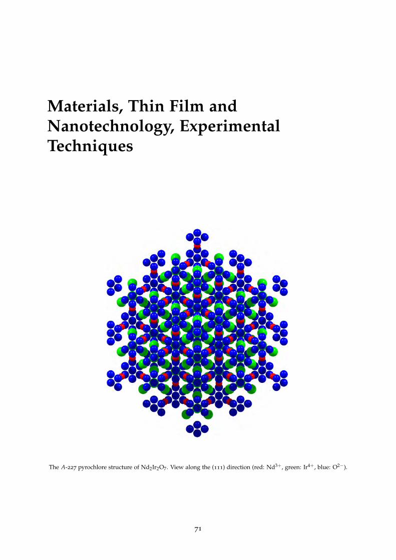
Materials, Thin Film andNanotechnology, ExperimentalTechniques
The A-227 pyrochlore structure of Nd2Ir2O7. View along the (111) direction (red: Nd3+, green: Ir4+, blue: O2−).
71


Annual Report 2013 73
Pyrochlore Iridates: Candidates for the Realization of Weyl Nodes?
S. Geprägs, A. Wörfel, M. Lammel, A. Habel, K. Helm-Knapp, M. Opel, R. Gross
Pyrochlore iridates A2Ir2O7 (A = Y or rare earth ion) offer a promising playground for thestudy of strong spin-orbit coupling, electronic correlations, and band topology effects. Novelphases such as axial or topological insulators have been predicted for these compounds [1].In particular, Nd2Ir2O7 is proposed to exhibit Weyl semimetal nodes [2] where two non-degenerated bands touch each other, creating a local linear dispersion in analogy to graphene.However, these nodes occur inside a fully three-dimensional solid and are topologically pro-tected, making Weyl states absolutely robust to perturbations [3].
100
101
1 10 100
100
T (K)
R(m
Ω)
µ0H=0Tµ0H=15T
M(k
A/m
)
FCZFC
µ0H=100mT
(a)
(b)
Figure 1: Temperature dependence of (a) the elec-tric resistance measured at different magnetic fieldsand (b) the magnetization recorded at µ0H = 100 mTunder zero field-cooled (ZFC) and field-cooled (FC)conditions for polycrystalline Nd2Ir2O7. The metal-to-insulator transition at T ' 33 K is marked by theblue dashed line. The inset in (a) shows the crystallo-graphic unit cell of the pyrochlore structure (red: Nd,green: Ir, blue: O). The corner-sharing tetrahedra ofthe Nd3+ ions are highlighted in the inset of (b).
In the cubic pyrochlore iridates, the magneticA3+ and Ir4+ ions reside on two distinct inter-penetrating sublattices of corner-sharing tetra-hedra (see insets of Fig. 1) [4]. Due to thethreefold rings in the two sublattices, the mag-netic interaction is highly frustrated. With in-creasing ionic radius of the A3+ ion, differ-ent ground states of A2Ir2O7 were observedin the pioneering work of Matsuhira et al. [5].While for Pr2Ir2O7 the ground state is metallic,a metal-insulator transition (MIT) was observedfor heavier rare earth ions like A = Nd, Sm, orEu at low temperatures. This MIT is accompa-nied by a bifurcation of the magnetic suscep-tibility under field-cooled (FC) and zero field-cooled (ZFC) conditions, suggesting the exis-tence of a magnetic long-range ordered state fortemperatures T < TMIT [6]. However, recentlya different temperature dependence of the elec-tric resistivity as well as the remanent magneti-zation was reported for Nd2Ir2O7 [7, 8].
To resolve this discrepancy, we fabricated poly-crystalline bulk samples of Nd2Ir2O7 by a stan-dard solid state reaction, using Nd2O3 and Irpowder as starting materials. The stoichiomet-ric mixture was reacted at temperatures be-tween 900
C and 1125C with several interme-
diate grindings. From X-ray diffraction, no par-asitic phases were detected. The lattice constantof bulk Nd2Ir2O7 was determined by Nelson-Riley extrapolation to a = (1.0376± 0.0001) nm,which is comparable to literature values [7]. The temperature dependence of the electric resis-tance was measured using a standard van der Pauw geometry. Figure 1(a) reveals a clear MITat around TMIT ' 33 K. Furthermore, a negative magnetoresistance was detected for tempera-tures T < TMIT. From SQUID magnetometry, the magnetization as a function of temperaturediffers for T < TMIT, depending on zero field-cooled or field-cooled conditions (cf. Fig. 1(b)).These results point to the presence of a magnetic long-range order below TMIT, confirming theinitial measurements by Matsuhira et al. [5]. However, the origin of the MIT is still unclearand has to be investigated in the future.
Measurements of the optical conductivity by Ueda et al. [9] revealed that Nd2Ir2O7 is indeed
2013

74 Walther–Meißner–Institut
close to a Weyl semimetal state, but still behaves like a Mott insulator at low temperatures.To stabilize such a Weyl semimetal state in Nd2Ir2O7, one might take advantage of epitaxialstrain in thin film samples. One prominent example is HgTe which shows a transition froma normal to a topological insulator when strained. For the first time in literature, we reporthere on epitaxial Nd2Ir2O7 thin films deposited on single crystalline Y:ZrO2 (YSZ) substratesby pulsed laser deposition from a stoichiometric, polycrystalline target [10]. The growth pa-rameters were optimized with respect to the crystalline properties of the Nd2Ir2O7 thin films.Optimum growth was obtained for a substrate temperature of 750C, an oxygen atmosphereof 25× 10−3 mbar, and a laser fluence of 2 J/cm2.
-0.01 0.00 0.01I (cps) qH (rlu)
107 103
0.94
0.96
0.98
1.00
1.02
q L(r
lu)
102
104
106
qL=0.9866
qL=1.0
q H=0
.0I(
cps)
Figure 2: Reciprocal space map and correspondingq-scans of a 27.5 nm thick Nd2Ir2O7 film on a YSZsubstrate around the YSZ(111) reflection.
The structural properties of the thin film sam-ples were investigated by high-resolution X-ray diffractometry. Figure 2 displays diffrac-tion scans around the YSZ(111) reflection froma 27.5 nm thick Nd2Ir2O7 thin film. Obviously,the reciprocal space map as well as the cor-responding qL-scan at qH = 0.0 depicted inthe left panel of Fig. 2 reveal a high crystallinequality, since finite thickness fringes are visibleover the whole investigated reciprocal space,demonstrating an excellent coherent growth.Furthermore, the thin film exhibits a low mo-saic spread which can be quantified by the fullwidth at half maximum (FWHM) of the qH-scan measured at qL = 0.9866 rlu, shown inthe upper panel of Fig. 2. A value of FWHM= 6.809× 10⁻⁴ rlu is obtained, corresponding to0.04
for standard ω rocking curve scans. Thus,the X-ray diffraction measurements indicate acoherent growth with low interface and surfaceroughness. The latter is further evidenced by
atomic force microscopy measurements (not shown here) which reveal a surface roughness ofonly 0.7 nm (rms value).
In forthcoming experiments, we will systematically investigate the magnetic and magneto-electric transport properties as a function of the strain state in Nd2Ir2O7 thin films. To thisend, the key objective is to possibly tune the ground state of Nd2Ir2O7 from a Mott insulatorstate to a Weyl semimetal.
References
[1] X. Wan, A. M. Turner, A. Vishwanath, and S. Y. Savrasov, Phys. Rev. B 83, 205101 (2011).[2] G. Chen, and M. Hermele, Phys. Rev. B 86, 235129 (2012).[3] L. Lu, L. Fu, J. D. Joannopoulos, and M. Soljacic, Nature Photon. 7, 294–299 (2013).[4] J. S. Gardner, M. J. P. Gingras, and J. E. Greedan, Rev. Mod. Phys. 82, 53–107 (2010).[5] K. Matsuhira, M. Wakeshima, Y. Hinatsu, and S. Takagi, J. Phys. Soc. Jpn. 80, 094701 (2011).[6] K. Tomiyasu, K. Matsuhira, K. Iwasa, M. Watahiki, S. Takagi, M. Wakeshima, Y. Hinatsu, M. Yokoyama, K.
Ohoyama, and K. Yamada, J. Phys. Soc. Jpn. 81, 034709 (2012).[7] S. M. Disseler, C. Dhital, T. C. Hogan, A. Amato, S. R. Giblin, C. de la Cruz, A. Daoud-Aladine, S. D. Wilson,
and M. J. Graf, Phys. Rev. B 85, 174441 (2012).[8] S. M. Disseler, S. R. Giblin, C. Dhital, K. C. Lukas, S. D. Wilson, and M. J. Graf, Phys. Rev. B 87, 060403
(2013).[9] K. Ueda, J. Fujioka, Y. Takahashi, T. Suzuki, S. Ishiwata, Y. Taguchi, and Y. Tokura, Phys. Rev. Lett. 109,
136402 (2012).[10] M. R. Lammel. Nd2Ir2O7: A new Weyl semimetal? Bachelor thesis, TU München (2013).
© Walther-Meißner-Institut

Annual Report 2013 75
Progress in the WMI Quantum Laboratory K04
J. Goetz, F. Wulschner, J. Höß, K. Neumaier, C. Probst, F. Deppe, A. Marx, R. Gross 1
Figure 1: Photograph of the dilution refrigerator with the new dewar dur-ing the experiment.
Last year, we reported onfirst cool-downs of a new liq-uid helium-precooled dilutionrefrigerator designed for ex-periments on superconduct-ing quantum circuits. Thenew fridge is set up inthe WMI Quantum Labora-tory K04 [1]. In 2013, the sys-tems has been completed andoptimized. Here, we report onthe improvement of the cool-ing power as well as the in-stallation of a new liquid he-lium dewar and measurementequipment (see Fig. 1). Thesesteps have lead to first success-ful experiments (see report byF. Wulschner et al., pp. 65–66).
By installing a suitable bypassbetween the exhaust of theturbomolecular pump and themechanical prepump we haveimproved the cooling powerof the new dilution refrigera-tor. By this simple measurewe avoid to pump through thegas handling system with itslarge flow impedance. Thisimpedance reduction results in a lower pressure at the output of the distillation line whichallows for a larger 3He throughput. With this improvement, the cooling power of the mixingchamber was increased by a factor of almost two to 140 µW at 100 mK.
Additionally, we have equipped the cryostat with eight coaxial measurement lines down to themixing chamber stage suitable for microwave frequencies. These lines are thermally anchoredat 4 K, 1.5 K, the still plate (200 mK), and the sample stage. We use low-loss silver-coatedcopper-clad steel cables from room temperature to the 4 K-stage. As a consequence, the he-lium consumption increases by 5 l per day. From the 4 K stage to the sample stage, we usephosphor bronze cables with niobium center conductor. Currently, four of the lines are usedas attenuated input lines and four as output lines. The latter are passing a series of cold cir-culators and four ultra low-noise high electron mobility transistor (HEMT) amplifiers. In thisway, we can mount up to four samples simultaneously to the sample stage. For the future it isplanned to expand the number of input lines to be able to set up more complex experiments.
To provide more space at the sample stage, a larger vacuum pot is used. In this way, we canextend the length of the sample stage from 5 cm to approximately 30 cm (see Fig. 2). In this
1We acknowledge financial support from the German Research Foundation via SFB 631, the German ExcellenceInitiative via NIM, and the EU projects CCQED and PROMISCE.
2013
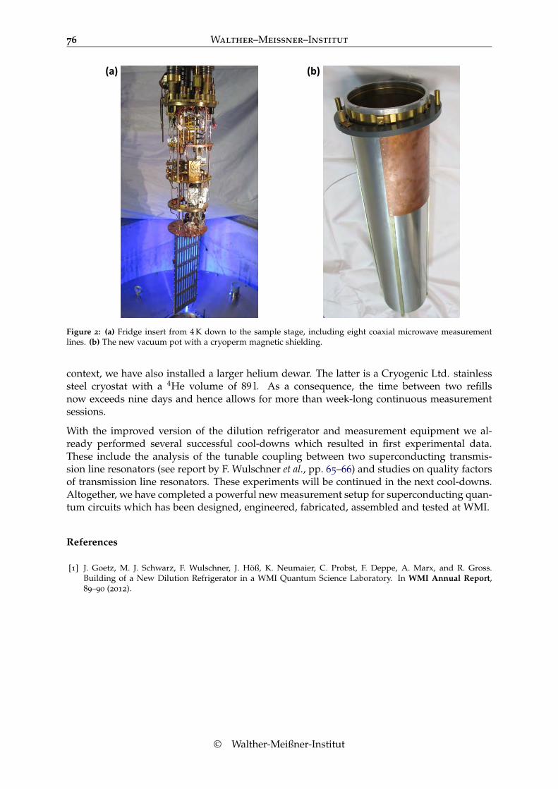
76 Walther–Meißner–Institut
(a) (b)
Figure 2: (a) Fridge insert from 4 K down to the sample stage, including eight coaxial microwave measurementlines. (b) The new vacuum pot with a cryoperm magnetic shielding.
context, we have also installed a larger helium dewar. The latter is a Cryogenic Ltd. stainlesssteel cryostat with a 4He volume of 89 l. As a consequence, the time between two refillsnow exceeds nine days and hence allows for more than week-long continuous measurementsessions.
With the improved version of the dilution refrigerator and measurement equipment we al-ready performed several successful cool-downs which resulted in first experimental data.These include the analysis of the tunable coupling between two superconducting transmis-sion line resonators (see report by F. Wulschner et al., pp. 65–66) and studies on quality factorsof transmission line resonators. These experiments will be continued in the next cool-downs.Altogether, we have completed a powerful new measurement setup for superconducting quan-tum circuits which has been designed, engineered, fabricated, assembled and tested at WMI.
References
[1] J. Goetz, M. J. Schwarz, F. Wulschner, J. Höß, K. Neumaier, C. Probst, F. Deppe, A. Marx, and R. Gross.Building of a New Dilution Refrigerator in a WMI Quantum Science Laboratory. In WMI Annual Report,89–90 (2012).
© Walther-Meißner-Institut
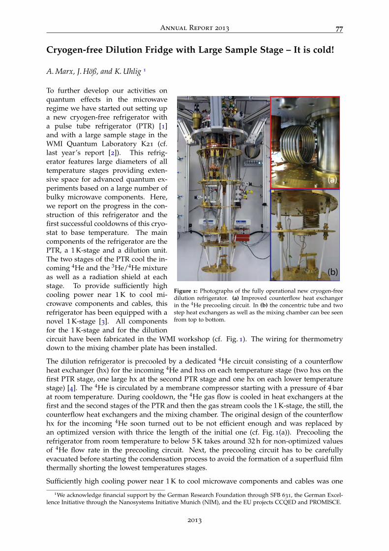
Annual Report 2013 77
Cryogen-free Dilution Fridge with Large Sample Stage – It is cold!
A. Marx, J. Höß, and K. Uhlig 1
Figure 1: Photographs of the fully operational new cryogen-freedilution refrigerator. (a) Improved counterflow heat exchangerin the 4He precooling circuit. In (b) the concentric tube and twostep heat exchangers as well as the mixing chamber can bee seenfrom top to bottom.
To further develop our activities onquantum effects in the microwaveregime we have started out setting upa new cryogen-free refrigerator witha pulse tube refrigerator (PTR) [1]and with a large sample stage in theWMI Quantum Laboratory K21 (cf.last year’s report [2]). This refrig-erator features large diameters of alltemperature stages providing exten-sive space for advanced quantum ex-periments based on a large number ofbulky microwave components. Here,we report on the progress in the con-struction of this refrigerator and thefirst successful cooldowns of this cryo-stat to base temperature. The maincomponents of the refrigerator are thePTR, a 1 K-stage and a dilution unit.The two stages of the PTR cool the in-coming 4He and the 3He/4He mixtureas well as a radiation shield at eachstage. To provide sufficiently highcooling power near 1 K to cool mi-crowave components and cables, thisrefrigerator has been equipped with anovel 1 K-stage [3]. All componentsfor the 1 K-stage and for the dilutioncircuit have been fabricated in the WMI workshop (cf. Fig. 1). The wiring for thermometrydown to the mixing chamber plate has been installed.
The dilution refrigerator is precooled by a dedicated 4He circuit consisting of a counterflowheat exchanger (hx) for the incoming 4He and hxs on each temperature stage (two hxs on thefirst PTR stage, one large hx at the second PTR stage and one hx on each lower temperaturestage) [4]. The 4He is circulated by a membrane compressor starting with a pressure of 4 barat room temperature. During cooldown, the 4He gas flow is cooled in heat exchangers at thefirst and the second stages of the PTR and then the gas stream cools the 1 K-stage, the still, thecounterflow heat exchangers and the mixing chamber. The original design of the counterflowhx for the incoming 4He soon turned out to be not efficient enough and was replaced byan optimized version with thrice the length of the initial one (cf. Fig. 1(a)). Precooling therefrigerator from room temperature to below 5 K takes around 32 h for non-optimized valuesof 4He flow rate in the precooling circuit. Next, the precooling circuit has to be carefullyevacuated before starting the condensation process to avoid the formation of a superfluid filmthermally shorting the lowest temperatures stages.
Sufficiently high cooling power near 1 K to cool microwave components and cables was one
1We acknowledge financial support by the German Research Foundation through SFB 631, the German Excel-lence Initiative through the Nanosystems Initiative Munich (NIM), and the EU projects CCQED and PROMISCE.
2013
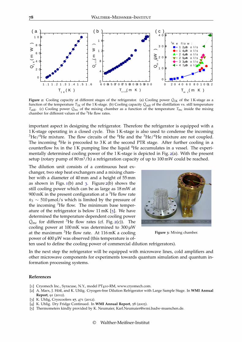
78 Walther–Meißner–Institut
1 . 1 1 . 2 1 . 3 1 . 4 1 . 5 1 . 60
2 0
4 0
6 0
8 0
1 0 0
0 2 0 4 0 6 0 8 0 1 0 0 1 2 00
1 0 0
2 0 0
3 0 0
4 0 0
6 0 0 6 5 0 7 0 0 7 5 0 8 0 0 8 5 0 9 0 00
4
8
1 2
1 6
( b )
Q 1K
(mW)
T 1 K ( K )
( a )
Q mc (µ
W)
T m c ( m K )
3 H e f l o w : 1 2 1 µm o l / s 1 4 7 µm o l / s 2 4 8 µm o l / s 2 9 4 µm o l / s 3 3 6 µm o l / s 4 7 0 µm o l / s
( c )
Q still (m
W)T s t i l l ( m K )
Figure 2: Cooling capacity at different stages of the refrigerator. (a) Cooling power Q1K of the 1 K-stage as afunction of the temperature T1K of the 1 K-stage. (b) Cooling capacity Qstill of the distillation vs. still temperatureTstill. (c) Cooling power Qmc of the mixing chamber as a function of the temperature Tmc inside the mixingchamber for different values of the 3He flow rates.
important aspect in designing the refrigerator. Therefore the refrigerator is equipped with a1 K-stage operating in a closed cycle. This 1 K-stage is also used to condense the incoming3He/4He mixture. The flow circuits of the 4He and the 3He/4He mixture are not coupled.The incoming 4He is precooled to 3 K at the second PTR stage. After further cooling in acounterflow hx in the 1 K pumping line the liquid 4He accumulates in a vessel. The experi-mentally determined cooling power of the 1 K-stage is depicted in Fig. 2(a). With the presentsetup (rotary pump of 80 m3/h) a refrigeration capacity of up to 100 mW could be reached.
Figure 3: Mixing chamber.
The dilution unit consists of a continuous heat ex-changer, two step heat exchangers and a mixing cham-ber with a diameter of 40 mm and a height of 55 mmas shown in Figs. 1(b) and 3. Figure 2(b) shows thestill cooling power which can be as large as 18 mW at900 mK in the present configuration at a 3He flow raten3 ∼ 510 µmol/s which is limited by the pressure ofthe incoming 3He flow. The minimum base temper-ature of the refrigerator is below 11 mK [5]. We havedetermined the temperature dependent cooling powerQmc for different 3He flow rates (cf. Fig. 2(c)). Thecooling power at 100 mK was determined to 300 µWat the maximum 3He flow rate. At 116 mK a coolingpower of 400 µW was observed (this temperature is of-ten used to define the cooling power of commercial dilution refrigerators).
In the next step the refrigerator will be equipped with microwave lines, cold amplifiers andother microwave components for experiments towards quantum simulation and quantum in-formation processing systems.
References
[1] Cryomech Inc., Syracuse, N.Y., model PT410-RM, www.cryomech.com.[2] A. Marx, J. Höß, and K. Uhlig. Cryogen-free Dilution Refrigerator with Large Sample Stage. In WMI Annual
Report, 91 (2012).[3] K. Uhlig, Cryocoolers 17, 471 (2012).[4] K. Uhlig. Dry Fridge Continued. In WMI Annual Report, 58 (2005).[5] Thermometers kindly provided by K. Neumaier, [email protected].
© Walther-Meißner-Institut
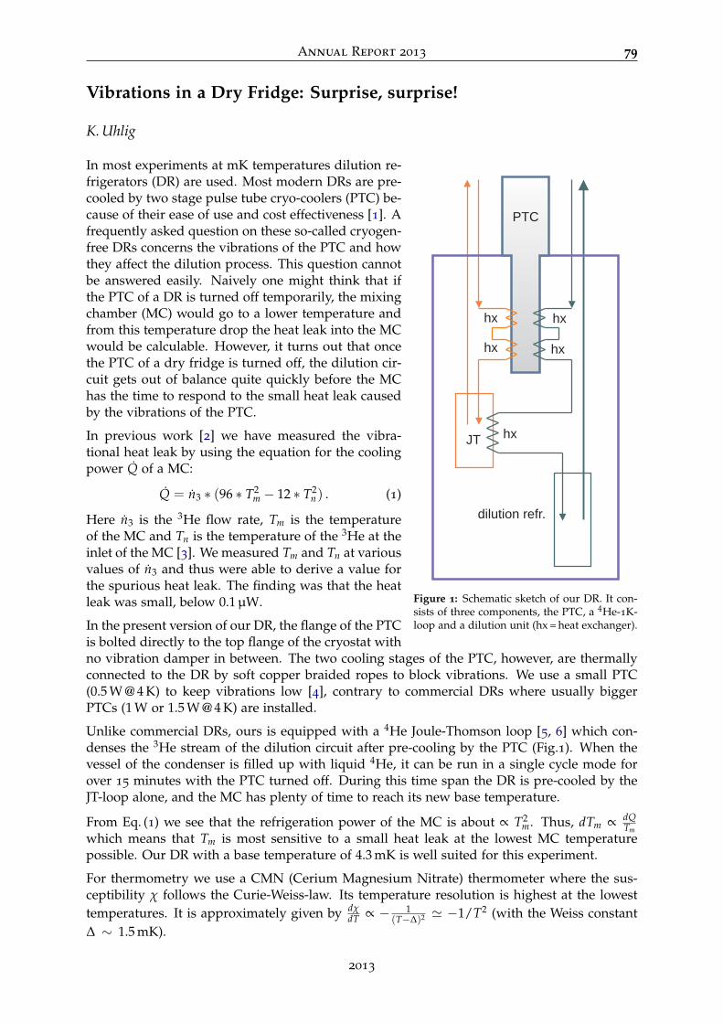
Annual Report 2013 79
Vibrations in a Dry Fridge: Surprise, surprise!
K. Uhlig
JT
PTC
dilution refr.
hx
hx hx
hx
hx
Figure 1: Schematic sketch of our DR. It con-sists of three components, the PTC, a 4He-1K-loop and a dilution unit (hx = heat exchanger).
In most experiments at mK temperatures dilution re-frigerators (DR) are used. Most modern DRs are pre-cooled by two stage pulse tube cryo-coolers (PTC) be-cause of their ease of use and cost effectiveness [1]. Afrequently asked question on these so-called cryogen-free DRs concerns the vibrations of the PTC and howthey affect the dilution process. This question cannotbe answered easily. Naively one might think that ifthe PTC of a DR is turned off temporarily, the mixingchamber (MC) would go to a lower temperature andfrom this temperature drop the heat leak into the MCwould be calculable. However, it turns out that oncethe PTC of a dry fridge is turned off, the dilution cir-cuit gets out of balance quite quickly before the MChas the time to respond to the small heat leak causedby the vibrations of the PTC.
In previous work [2] we have measured the vibra-tional heat leak by using the equation for the coolingpower Q of a MC:
Q = n3 ∗ (96 ∗ T2m − 12 ∗ T2
n) . (1)
Here n3 is the 3He flow rate, Tm is the temperatureof the MC and Tn is the temperature of the 3He at theinlet of the MC [3]. We measured Tm and Tn at variousvalues of n3 and thus were able to derive a value forthe spurious heat leak. The finding was that the heatleak was small, below 0.1 µW.
In the present version of our DR, the flange of the PTCis bolted directly to the top flange of the cryostat withno vibration damper in between. The two cooling stages of the PTC, however, are thermallyconnected to the DR by soft copper braided ropes to block vibrations. We use a small PTC(0.5 W @ 4 K) to keep vibrations low [4], contrary to commercial DRs where usually biggerPTCs (1 W or 1.5 W @ 4 K) are installed.
Unlike commercial DRs, ours is equipped with a 4He Joule-Thomson loop [5, 6] which con-denses the 3He stream of the dilution circuit after pre-cooling by the PTC (Fig.1). When thevessel of the condenser is filled up with liquid 4He, it can be run in a single cycle mode forover 15 minutes with the PTC turned off. During this time span the DR is pre-cooled by theJT-loop alone, and the MC has plenty of time to reach its new base temperature.
From Eq. (1) we see that the refrigeration power of the MC is about ∝ T2m. Thus, dTm ∝ dQ
Tmwhich means that Tm is most sensitive to a small heat leak at the lowest MC temperaturepossible. Our DR with a base temperature of 4.3 mK is well suited for this experiment.
For thermometry we use a CMN (Cerium Magnesium Nitrate) thermometer where the sus-ceptibility χ follows the Curie-Weiss-law. Its temperature resolution is highest at the lowesttemperatures. It is approximately given by dχ
dT ∝ − 1(T−∆)2 ' −1/T2 (with the Weiss constant
∆ ∼ 1.5 mK).
2013
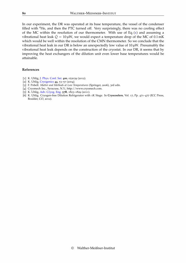
80 Walther–Meißner–Institut
In our experiment, the DR was operated at its base temperature, the vessel of the condenserfilled with 4He, and then the PTC turned off. Very surprisingly, there was no cooling effectof the MC within the resolution of our thermometer. With use of Eq. (1) and assuming avibrational heat leak Q = 10 µW, we would expect a temperature drop of the MC of 0.1 mKwhich would be well within the resolution of the CMN thermometer. So we conclude that thevibrational heat leak in our DR is below an unexpectedly low value of 10 µW. Presumably thevibrational heat leak depends on the construction of the cryostat. In our DR, it seems that byimproving the heat exchangers of the dilution unit even lower base temperatures would beattainable.
References
[1] K. Uhlig, J. Phys. Conf. Ser. 400, 052039 (2012).[2] K. Uhlig, Cryogenics 44, 53–57 (2004).[3] F. Pobell. Matter and Methods at Low Temperatures (Springer, 2006), 3rd edn.[4] Cryomech Inc., Syracuse, N.Y.; http://www.cryomech.com.[5] K. Uhlig, Adv. Cryog. Eng. 57B, 1823–1829 (2011).[6] K. Uhlig. Cryogen-free Dilution Refrigerator with 1K Stage. In Cryocoolers, Vol. 17, Pp. 471–477 (ICC Press,
Boulder, CO, 2012).
© Walther-Meißner-Institut
Experimental Facilities
81

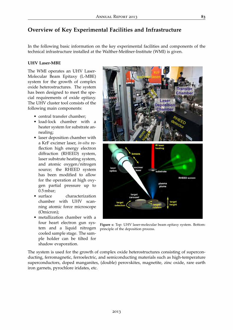
Annual Report 2013 83
Overview of Key Experimental Facilities and Infrastructure
In the following basic information on the key experimental facilities and components of thetechnical infrastructure installed at the Walther-Meißner-Institute (WMI) is given.
TransferChamber
LaserDepositionChamber
laserport
RHEEDdetector
atom
sour
ce
KrFexcimer laser
Figure 1: Top: UHV laser-molecular beam epitaxy system. Bottom:principle of the deposition process.
UHV Laser-MBE
The WMI operates an UHV Laser-Molecular Beam Epitaxy (L-MBE)system for the growth of complexoxide heterostructures. The systemhas been designed to meet the spe-cial requirements of oxide epitaxy.The UHV cluster tool consists of thefollowing main components:
• central transfer chamber;• load-lock chamber with a
heater system for substrate an-nealing;
• laser deposition chamber witha KrF excimer laser, in-situ re-flection high energy electrondiffraction (RHEED) system,laser substrate heating system,and atomic oxygen/nitrogensource; the RHEED systemhas been modified to allowfor the operation at high oxy-gen partial pressure up to0.5 mbar;
• surface characterizationchamber with UHV scan-ning atomic force microscope(Omicron);
• metallization chamber with afour heart electron gun sys-tem and a liquid nitrogencooled sample stage. The sam-ple holder can be tilted forshadow evaporation.
The system is used for the growth of complex oxide heterostructures consisting of supercon-ducting, ferromagnetic, ferroelectric, and semiconducting materials such as high-temperaturesuperconductors, doped manganites, (double) perovskites, magnetite, zinc oxide, rare earthiron garnets, pyrochlore iridates, etc.
2013

84 Walther–Meißner–Institut
Figure 2: Pulsed Laser Deposition (PLD): Whenthe pulse of the UV laser (KrF excimer laser,248 nm) hits the target, the target material is ab-lated and the so-called laser “plume” containinghighly excited atoms and molecules is formed.
The original laser molecular beam epitaxy system(laser-MBE) designed already in 1995/96 has beencontinuously upgraded and modified until now.In particular, the substrate heating system and thetemperature control unit were changed from a re-sistive radiation heater to an infrared laser heatingsystem (see Fig. 3, left) including a pyrometer fordetermining the sample temperature. In addition,a source for atomic oxygen and nitrogen has beeninstalled. The main advantage of the new heatingsystem is that only the substrate is heated whilethe surrounding parts are hardly affected (Fig. 3,right). In this way one can achieve a substantiallybetter vacuum at temperatures well above 1000 C.The achievable substrate temperature is limited bythe melting point and the size of the substrate ma-terial (approx. 1410 C for a 5× 5 mm2 silicon sub-strate). The laser heating system has already beensuccessfully used for removing the amorphous sil-icon oxide layer from the surface of silicon sub-strates at 1150 C.
Figure 3: Components of the laser heating system: The substrate is heated using an IR diode laser head that islocated in a separate box far away from the deposition chamber (left). The laser light is brought to the substrate(right) via an optical fiber.
We have further developed and installed a home-made telescope zoom optics for the pulsedUV laser light, consisting of in total five lenses on sliding lens holders allowing for a movementover a total distance of 1200 mm. The lens holders are attached to independent stepper motors,each connected to a controller providing an accurate positioning precision. The controllersare driven via a PC, thus allowing for a full automation of the lens system itself. With thistelescope zoom optics we are able to change the area of the UV laser spot on the target,resulting in an accessible range of laser fluences from ρL = 0.5 J/cm2 to 5 J/cm2. To maintaina stable laser fluence at the target, we have installed a so-called intelligent window (PVDProducts) at the laser entrance port combining two unique features. First, it keeps the innerside of the entrance window free of coatings by blocking the ablated plasma plume via arotatable disc consisting of UV grade fused silica. Second, an insertable mirror positionedin the light path after the disc allows to guide the incoming UV laser pulse through a sidewindow, where its energy is determined by a pyroelectric detector. These measures helpto improve the deposition processes by accurately monitoring ρL as one of the most criticalprocess parameters.
© Walther-Meißner-Institut

Annual Report 2013 85
UHV Electron Beam Evaporation System
Figure 4: (a) Photograph of the UHV electron beam evaporation system. (b) Manipulator with UHV steppingmotors for automated and precise sample tilt and options for rotation.
The UHV metal MBE system allows for the growth of high quality metallic thin films byelectron beam evaporation and molecular beam epitaxy. The system is optimized for thefabrication of superconducting persistent current qubits by aluminum shadow evaporation. Itis equipped with an improved substrate holder allowing for multi-angle shadow evaporation.The main components of the system are:
• UHV system with a process chamber with a base pressure of ∼ 1× 10⁻⁸ mbar pumpedby a 1000 l/s turbo molecular pump with magnetic suspension of the rotor adequate forcorrosive gases.
• Load-lock chamber equipped with a magnetic transfer system (push-pull positioner) forsample transfer without breaking the vacuum in the process chamber.
• Downstream pressure control by an adaptive pressure controlled gate valve.• Electron beam evaporator with six 8 cm3 crucibles embedded in a linearly movable water
cooled rail providing six different materials.• Film thickness measurement and closed loop evaporation rate control by a quartz crystal
microbalance in combination with the evaporation controller.• Effusion cell for molecular beam epitaxy processes.• Ion sputtering gun for in-situ sample cleaning• Manipulator with UHV stepping motors for automated and precise sample tilt and op-
tions for rotating and cooling the sample.
A precise and reproducible tilt of the sample is realized by a sample manipulator with processspecific degrees of freedom. The downstream pressure control allows for a fast adjustmentand precise control of the oxygen partial pressure. This is crucial for a well-defined oxidationprocess of the Josephson junctions barriers. The entire process can be performed fully auto-mated via a touch screen and is controlled by a LabView program. Up to six effusion cells canbe optionally added to the system allowing for further materials. The manipulator allows forfurther degrees of freedom that can be used to align the sample to the effusion cells, the ionsputtering gun and to measuring equipment such as ellipsometry or RHEED.
2013

86 Walther–Meißner–Institut
Single Crystal Growth and Synthesis of Bulk Materials
Figure 5: The four-mirror image furnace installed at thecrystal laboratory of the WMI. Crystals can be grown bythe floating zone and traveling solvent floating zone tech-niques at temperatures up to 2200 C and pressures up to10 bar.
Transition metal oxides are of great inter-est due to their various interesting physicalproperties (e.g. high temperature supercon-ductivity, colossal magnetoresistance, ferro-electricity, nonlinear optical properties etc.)and their high potential for applications.Therefore, the WMI operates a laboratory forthe synthesis of bulk materials and singlecrystals of transition metal oxides. Besidesvarious chamber- and tube furnaces a four-mirror image furnace is used for the crys-tal growth of various oxide systems. Withthis furnace crystals of many different com-pounds of the high temperature supercon-ductors and various other transition metaloxides have been grown as single crystals us-ing the traveling solvent floating zone tech-nique. The furnace consists basically of 4
elliptical mirrors with a common focus onthe sample rod and with halogen lamps intheir other focus. By irradiation of the fo-cused light the sample rod is locally heatedand eventually molten. The molten zone canbe moved up and down along the entire sam-ple rod under simultaneous rotation. Due tothe anisotropic growth velocity a preferen-tial growth of those grains with the fastestgrowth velocity along the pulling directionis obtained and the formerly polycrystallinerod is transformed into a single crystal. Single crystal growth can be performed with thisfurnace at maximum temperatures up to 2200 C in the pressure range from 10−5 mbar up to10 bar and in oxidizing, reducing as well as inert atmosphere.
Figure 6: Left: Central part of the image furnace with four elliptical mirrors. In the center one can see thequartz tube with a polycrystalline rod. Right: View on the molten zone of Pr2−xCexCuO4 (melting point: 1280 C)obtained by a CCD camera.
© Walther-Meißner-Institut

Annual Report 2013 87
Figure 7: The two-circle X-ray diffractometer Bruker D8 Advance.
The X-ray diffraction systems
For X-ray analysis the Walther-Meissner-Institute operates twoX-ray diffractometers (BrukerD8 Advance and D8 Discover).The two-circle system is usedfor powder diffraction. In thissystem the samples can beheated in oxygen atmosphereup to 1600 C. It is equippedwith a Göbel mirror and anarea detector to save measuringtime. The second system isa high resolution four-circlediffractometer that can be usedfor reciprocal space mappings. Itis equipped with a Göbel mirrorand an asymmetric two-fold Gemonochromator and allows forthe texture analysis of thin filmsuperlattices and single crys-talline materials. In both systemsmeasurements can be carried outfully computer controlled.
Beside these two Bruker X-raysystems a Laue camera for sin-gle crystal analysis and a Debye-Scherrer camera are available.
Figure 8: Left: High temperature sample holder of the D8 Advance system. Right: Four-circle high resolutionX-ray diffractometer Bruker D8 Discover.
2013

88 Walther–Meißner–Institut
Figure 9: Quantum Design SQUID magnetometer.
The SQUID magnetometer
For the analysis of the magneticproperties of materials, a QuantumDesign SQUID magnetometer sys-tem (Fig. 9) is operated at the WMI.The SQUID magnetometer allowsfor measurements in the tempera-ture regime from 1.8 to 400 K andprovides excellent sensitivity par-ticularly in the low field regime.Due to the excellent sensitivity ofthe system, thin film samples witha very small sample volume canbe analyzed. The SQUID magne-tometer is equipped with a super-conducting solenoid allowing for amaximum field of 7 T. At present,
the magnetometer is used for the characterization of magnetic and superconducting materials(both in bulk and thin film form). Examples are the cuprate high temperature superconduc-tors, the doped manganites, magnetite, the double perovskites, magnetic semiconductors, ormultiferroics.
Figure 10: High field laboratory with Oxford 17 T magnet system.
The High Field Laboratory
Transport and thermody-namic properties of samplesare often studied as a functionof the applied magnetic field.For such measurements sev-eral superconducting magnetsare available at the WMI. Twoof them (8/10 and 15/17 Teslamagnet system) are locatedin the high magnetic fieldlaboratory in the basementof the WMI. The magnetsystems are installed belowthe floor level to facilitatethe access to the top flangeand the change of the samplesticks. The magnet systemsare decoupled from the build-ing to avoid noise due tomechanical vibrations. A variety of sample holders can be mounted allowing for e.g. samplerotation during the measurement. For standard sample holders the accessible temperatureregime is 1.5 K < T < 300 K. However, also 3He/4He dilution refrigerator inserts (T > 20 mK)or high temperature units (T < 700 K) can be mounted. All measurements are fully computercontrolled (by the use of the LabView software tool) allowing for remote control and almostcontinuous measurements.
Since 2012, a 3D vector magnet with variable temperature insert, allowing for 2 T in-plane and6 T out-of-plane magnetic fields is available for thermal and electrical transport experiments.A further 3D vector magnet allowing for 1 T in-plane and 6 T out-of-plane magnetic fields is
© Walther-Meißner-Institut

Annual Report 2013 89
installed in the WMI Quantum Laboratories as part of a cryogen-free dilution system (seepage 93).
Figure 11: Top: Part of the clean room facility with optical lithographyequipment and clean room benches. Bottom: Resist coater and hot plates.
The Clean Room Facility
For the fabrication of nano-structures and superconduct-ing as well as spintronic de-vices the WMI operates a class1000 clean room facility withan area of about 50 m2. Thisclean room facility has beenput into operation at the WMIwithin the year 2001. Theclean room is subdivided intotwo parts for photolithogra-phy and electron beam lithog-raphy, respectively. The cleanroom facility is equippedwith the standard tools forphotolithography such as re-sist coaters, hot plates, wetbenches, a Karl Süss MJB3
mask aligner and an opti-cal projection lithography sys-tem. The technical infrastruc-ture for the clean room is lo-cated in the basement of theWMI directly below the cleanroom area.
Since 2005 the clean room alsois equipped with a reactiveion etching system, Plasmalab80 Plus with ICP plasmasource (Oxford InstrumentsPlasma Technology).
2013

90 Walther–Meißner–Institut
Figure 12: Top: Philips XL 30 SFEG Scanning Electron Microscope withRaith Elphy Plus Lithography System. Bottom: Raith Laser Stage.
Electron Beam Lithography
The Electron Beam Lithogra-phy System is installed in thesecond part of the clean roomfacility. It consists of a PhilipsXL 30 SFEG scanning elec-tron microscope (SEM) witha Raith Elphy Plus electronbeam lithography system anda laser interferometer tablefor precise stitching of writingfields.
The SEM is equipped with ahot field emitter and typicallyprovides a beam diameter ofless than 1.5 nm at ≥ 10 keVor about 2.5 nm at 1 keV. Thelithography unit allows thefabrication of nanostructuresdown to about 10 nm. Wehave realized the controlledfabrication of metallic strippatterns with a strip widthof about 20 nm. The elec-tron beam lithography is usedfor the fabrication of nanos-tructures in metallic and ox-ide systems required for thestudy of quantum effects inmesoscopic samples.
© Walther-Meißner-Institut

Annual Report 2013 91
Figure 13: Top: Süss MJB 3 maskaligner for optical lithography. Bottom:Optical projection lithography based on an optical microscope.
Optical Lithography
For photolithography, a KarlSüss MJB 3 maskaligner oran optical microscope basedprojection system are used.The maskaligner operates inthe 1 : 1 soft or hard con-tact mode and uses chromiummetal masks. In the projec-tion system the mask patternis demagnified by a factor of5 to 100. Therefore, cheap foilmasks can be used. With bothsystems microstructures witha lateral dimension down to1 µm can be fabricated.
2013

92 Walther–Meißner–Institut
Low and Ultra-Low Temperature Facilities
Figure 14: The “dry” dilution re-frigerator of the WMI.
Figure 15: Low-temperature unit ofa WMI dilution refrigerator readyto go into a cryostat.
At the WMI, we haveconstructed the first dilu-tion refrigerator with pulsetube pre-cooling for ultra-low temperature experi-ments. This type of re-frigerator works withoutcryo-liquids, and thus isa lot more practical, moreeconomical and more re-liable than cryostats withliquid helium pre-cooling.These days, all major cryo-engineering companies areoffering commercial ver-sions of this Millikelvincooler, and these so-called"dry" refrigerators outsellconventional refrigeratorsby a wide margin. Thegeneral construction con-cept of most manufactur-ers is unchanged from ouroriginal prototype, wherethe refrigerator consists of three basic components. The first cooling stage is a commer-cial pulse tube cryocooler which reaches a base temperature of 2.5 K. The second stage isa Joule-Thomson stage, and the last stage is a dilution refrigeration stage, where the lowesttemperature of the cryostat is about 0.01 K (Fig. 14).
Figure 16: Two mixing chamber mounting plates with silver sponges.Those are needed to overcome the thermal resistance (Kapitza resistance)between the liquid 3,4He and the mounting plate of the mixing chamber.To fabricate the mounting of the sponge (square pins embedded in thesponge) a spark erosion technique has been employed.
In many low temperature ap-plications high refrigerationcapacities are required. Ourdesign allows for a high circu-lation rate of 3He which in theend determines the coolingpower of a dilution refrigera-tor. Presently our "dry" fridgereaches a refrigeration capac-ity of 700 µW at a tempera-ture of the mixing chamber of0.1 K, seven times the coolingpower of the WMI nuclear de-magnetization cryostat. Goalsof our present work are a fur-ther increase of cooling powerand a lower base temperatureof the dry dilution refrigera-
tor. For a more detailed report, please see page 77.
A smaller version of our cryogen-free fridge has become commercially available by OxfordInstruments (formerly VeriCold Technologies, Ismaning). It has a refrigeration capacity of 250 µW
© Walther-Meißner-Institut

Annual Report 2013 93
at a mixing chamber temperature of 0.1 K (Fig. 15).
The WMI also develops and fabricates dilution refrigerator inserts for temperatures down toabout 20 mK. The inserts fit into all cryogenic systems (e.g. superconducting magnets) havinga two inch bore. They allow fast sample change and rapid cool down cycles of less than fivehours. The dilution refrigerator inserts are engineered and fabricated in-house and are alsoprovided to other low temperature laboratories for ultra-low temperature experiments.
Millikelvin Temperatures in Combination with 3D Vector Magnetic-Fields
Figure 17: The dilution refrigerator with the 3Dvector magnet located in the Quantum Labora-tories.
Part of the Quantum Laboratories at the Walther-Meißner-Institut is a cryogen-free dilution refriger-ator equipped with a 3D vector magnet allowingfor 1 T in-plane and 6 T out-of-plane magnetic fields.Additional microwave coaxial lines allow for the mi-crowave spectroscopy up to 18 GHz under these ex-perimental conditions.
Scientifically, several directions in the field of funda-mental light-matter interaction are envisaged:
(i) Circuit quantum electrodynamics (circuit QED),where superconducting qubits form hybrids withmicrowave resonators. These experiments are timeconsuming, because quantum effects arise in thelimit of low excitation numbers. Hereby, challengingrequirements are imposed on the detection systemsallowing to detect microwave signals in the attowattregime.
Figure 18: Inside of the dilu-tion system. The windows ofthe 4 K and the still shield areremoved providing access tothe low temperature stages.
(ii) Storage of quantum states. One possibility is the transfer ofthe quantum information contained in photons to long-lived spinstates. Additionally, exchange coupled systems or ferromagetic sys-tems come into focus, because the effective coupling strength scaleswith the square-root of the number of spins contributing. In gen-eral, we study the light-matter interaction with long-lived spin sys-tems and integrate superconducting quantum circuits.
(iii) Spin systems. Here, the investigations are not limited to para-magnetic spin systems, but will be extended to exchange coupled(ferro-) magnetic systems. Hereby, magnetization damping can beinvestigated as a function of temperature, frequency and magneticfield direction.
(iv) Circuit electro-mechanical hybrid systems consisting of a nano-mechanical element coupled to a superconducting microwave res-onator. In this context, sideband cooling of the mechanical systeminto its ground state and pulsed spectroscopy of hybrid system areperformed and will be extended.
2013
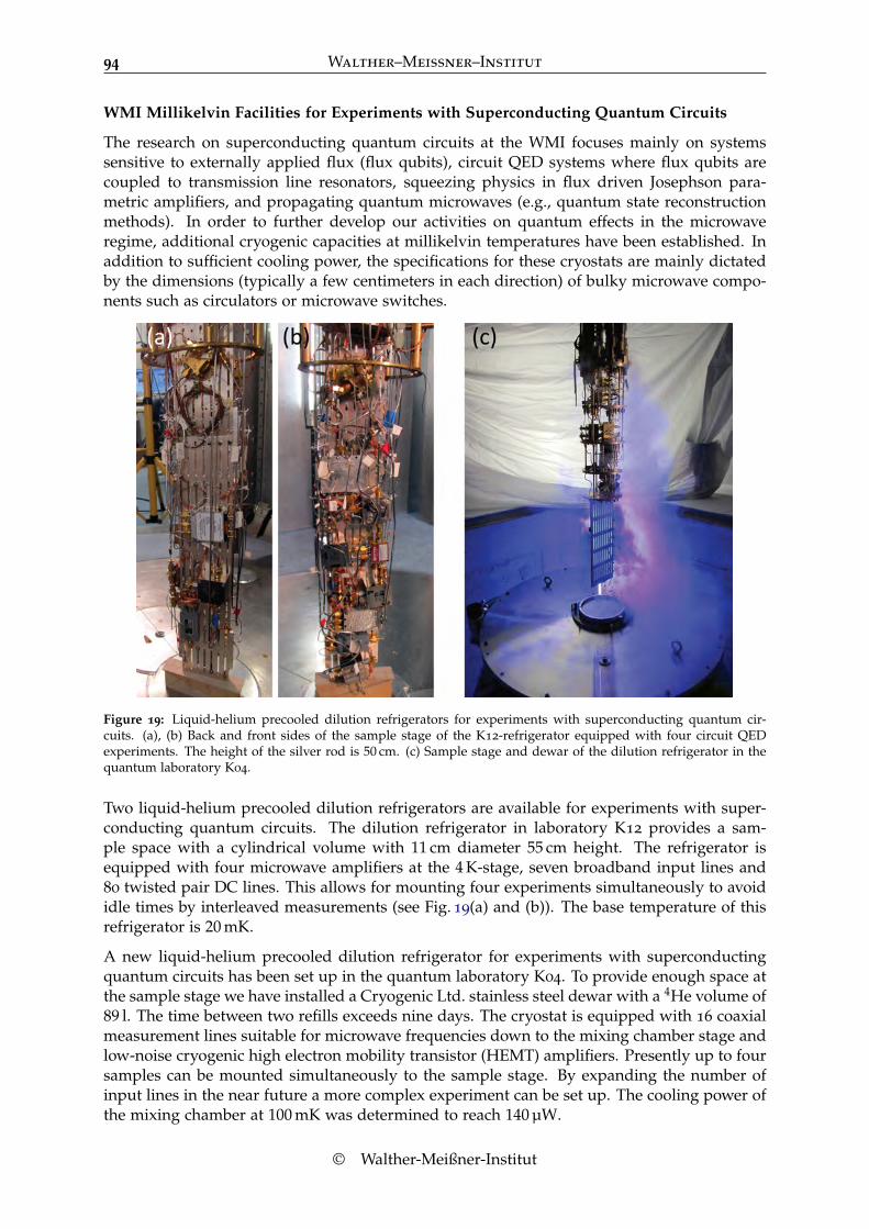
94 Walther–Meißner–Institut
WMI Millikelvin Facilities for Experiments with Superconducting Quantum Circuits
The research on superconducting quantum circuits at the WMI focuses mainly on systemssensitive to externally applied flux (flux qubits), circuit QED systems where flux qubits arecoupled to transmission line resonators, squeezing physics in flux driven Josephson para-metric amplifiers, and propagating quantum microwaves (e.g., quantum state reconstructionmethods). In order to further develop our activities on quantum effects in the microwaveregime, additional cryogenic capacities at millikelvin temperatures have been established. Inaddition to sufficient cooling power, the specifications for these cryostats are mainly dictatedby the dimensions (typically a few centimeters in each direction) of bulky microwave compo-nents such as circulators or microwave switches.
Figure 19: Liquid-helium precooled dilution refrigerators for experiments with superconducting quantum cir-cuits. (a), (b) Back and front sides of the sample stage of the K12-refrigerator equipped with four circuit QEDexperiments. The height of the silver rod is 50 cm. (c) Sample stage and dewar of the dilution refrigerator in thequantum laboratory K04.
Two liquid-helium precooled dilution refrigerators are available for experiments with super-conducting quantum circuits. The dilution refrigerator in laboratory K12 provides a sam-ple space with a cylindrical volume with 11 cm diameter 55 cm height. The refrigerator isequipped with four microwave amplifiers at the 4 K-stage, seven broadband input lines and80 twisted pair DC lines. This allows for mounting four experiments simultaneously to avoididle times by interleaved measurements (see Fig. 19(a) and (b)). The base temperature of thisrefrigerator is 20 mK.
A new liquid-helium precooled dilution refrigerator for experiments with superconductingquantum circuits has been set up in the quantum laboratory K04. To provide enough space atthe sample stage we have installed a Cryogenic Ltd. stainless steel dewar with a 4He volume of89 l. The time between two refills exceeds nine days. The cryostat is equipped with 16 coaxialmeasurement lines suitable for microwave frequencies down to the mixing chamber stage andlow-noise cryogenic high electron mobility transistor (HEMT) amplifiers. Presently up to foursamples can be mounted simultaneously to the sample stage. By expanding the number ofinput lines in the near future a more complex experiment can be set up. The cooling power ofthe mixing chamber at 100 mK was determined to reach 140 µW.
© Walther-Meißner-Institut

Annual Report 2013 95
Figure 20: Dry dilution refrigerator with a large samplespace.
A new cryogen-free dilution refrigeratorwith a pulse tube refrigerator (PTR) andwith a large sample stage has been set upin the quantum laboratory K21 using thelongstanding experience in dry dilution re-frigerators at the WMI. This refrigerator fea-tures large diameters (tens of centimeters) ofall temperature stages providing extensivespace for advanced quantum experiments.The main components of the refrigerator arethe PTR, a 1 K-stage and a dilution unit.The two stages of the PTR cool the incom-ing 4He and the 3He/4He mixture as well asone radiation shield at each stage. To pro-vide sufficiently high cooling power near 1 Kto cool microwave components and cables,this refrigerator has been equipped with a1 K-stage operating in a closed cycle. A re-frigeration capacity of the 1 K-stage of up to100 mW could be reached. The dilution re-frigerator is precooled by a dedicated 4Hecircuit. The minimum base temperature ofthe refrigerator is below 11 mK. The coolingpower at 100 mK was determined to reach300 µW at the maximum 3He flow rate.
2013

96 Walther–Meißner–Institut
© Walther-Meißner-Institut
Annual Report 2013 97
Publications
1. Alternative route to charge density wave formation in multiband systemssH.-M. Eiter, M. Lavagnini, R. Hackl, E.A. Nowadnick, A.F. Kemper, T.P. Devereaux, J.-H. Chu,J.G. Analytis, I.R. Fisher, L. DegiorgiPNAS 110, 64-69 (2013).
2. Tunable Coupling Engineering Between Superconducting Resonators: From Sidebands toEffective Gauge FieldsBorja Peropadre, David Zueco, Friedrich Wulschner, Frank Deppe, Achim Marx, Rudolf Gross,and Juan José García-RipollPhys. Rev. B 87, 134504 (2013).
3. Slowing, advancing and switching of microwave signals using circuit nanoelectromechanicsX. Zhou, F. Hocke, A. Schliesser, A. Marx, H. Huebl, R. Gross, and T. J. KippenbergNature Physics 9, 179-184 (2013).
4. Der Mann, mit dem die Kälte kam – Walther Meißner und die Tieftemperaturphysik inDeutschlandW. Buck, D. Einzel, R. GrossPhysik Journal 12, No. 5, 37–41 (2013).
5. Cryogen-free dilution refrigerator with 1 K-stageKurt UhligCryocoolers 17, 471 (2013).
6. Optimisation of NbN thin films on GaAs substrates for in-situ single photon detection instructured photonic devicesGünther Reithmaier, Jörg Senf, Stefan Lichtmannecker, Thorsten Reichert, Fabian Flassig, AndrejVoss, Rudolf Gross, Jonathan FinleyJ. Appl. Phys. 113, 143507 (2013).
7. High Cooperativity in Coupled Microwave Resonator Ferrimagnetic Insulator HybridsHans Huebl, Christoph Zollitsch, Johannes Lotze, Fredrik Hocke, Moritz Greifenstein, AchimMarx, Sebastian T. B. Goennenwein, and Rudolf GrossPhys. Rev. Lett. 111, 127003 (2013).
8. Gradiometric flux qubits with tunable gapM. J. Schwarz, J. Goetz, Z. Jiang, T. Niemczyk, F. Deppe, A. Marx, R. GrossNew J. Phys. 15, 045001 (2013).
9. Spin Hall Magnetoresistance Induced by a Non-Equilibrium Proximity EffectH. Nakayama, M. Althammer, Y.-T. Chen, K. Uchida, Y. Kajiwara, D. Kikuchi, T. Ohtani, S.Geprägs, M. Opel, S. Takahashi, R. Gross, G. E. W. Bauer, S. T. B. Goennenwein, E. SaitohPhys. Rev. Lett. 110, 206601 (2013).
10. Raman-Scattering Detection of Nearly Degenerate s-Wave and d-Wave Pairing Channels inIron-Based Ba0.6K0.4Fe2As2 and Rb0.8Fe1.6Se2 SuperconductorsFlorian Kretzschmar, Bernhard Muschler, Thomas Böhm, Andreas Baum, Rudi Hackl, Hai-HuWen, Vladimir Tsurkan, Joachim Deisenhofer, Alois LoidlPhys. Rev. Lett. 110, 187002 (2013).
11. On-chip time resolved detection of quantum dot emission using integrated superconductingsingle photon detectorsGünther Reithmaier, Stefan Lichtmannecker, Thorsten Reichert, Peter Hasch, Kai Müller, MaxBichler, Rudolf Gross, Jonathan J. FinleyScientific Reports 3, 1901 (2013).
12. Fast microwave beam splitters from superconducting resonatorsM. Haeberlein, D. Zueco, P. Assum, T. Weißl, E. Hoffmann, B. Peropadre, J.J. Garcia-Ripoll, E.Solano, F. Deppe, A. Marx, R. GrossarXiv:1302.0729, submitted for publication (2013).
13. Theory of spin Hall magnetoresistance
2013

98 Walther–Meißner–Institut
Yan-Ting Chen, Saburo Takahashi, Hiroyasu Nakayama, Matthias Althammer, Sebastian T. B.Goennenwein, Eiji Saitoh, Gerrit E. W. BauerPhys. Rev. B 87, 144411 (2013).
14. Quantitative Study of the Spin Hall Magnetoresistance in Ferromagnetic Insulator/NormalMetal HybridsM. Althammer, S. Meyer, H. Nakayama, M. Schreier, S. Altmannshofer, M. Weiler, H. Huebl, S.Geprägs, M. Opel, R. Gross, D. Meier, C. Klewe, T. Kuschel, J.-M. Schmalhorst, G. Reiss, L. Shen,A. Gupta, Y.-T. Chen, G.E.W. Bauer, E. Saitoh, S.T.B. GönnenweinPhys. Rev. B 87, 224401 (2013).
15. Converse Magnetoelectric Effects in Fe3O4/BaTiO3 Multiferroic HybridsS. Geprägs, D. Mannix, M. Opel, S.T.B. Goennenwein, R. GrossPhys. Rev. B 88, 054412 (2013).
16. Magnon, phonon, and electron temperature profiles and the spin Seebeck effect in magneticinsulator/normal metal hybrid structuresMichael Schreier, Akashdeep Kamra, Mathias Weiler, Jiang Xiao, Gerrit E. W. Bauer, RudolfGross, Sebastian T. B. GoennenweinPhys. Rev. B 88, 094410 (2013).
17. Localized states in the Mott insulator κ-(BEDT-TTF)2Cu[N(CN)2]Cl as probed by photolumi-nescenceN. Drichko, R. Hackl, and J. SchlueterPhys. Rev. B 88, 115109 (2013).
18. Separation of semiconducting and ferromagnetic FeSi2-nanoparticles by magnetic filteringWilli Aigner, Sabrina Niesar, Ervin Mehmedovic, Matthias Opel, Friedrich E. Wagner, HartmutWiggers, Martin StutzmannJ. Appl. Phys. 114, 134308 (2013).
19. Two-Fluid Description of Two-Band SuperconductorsNikolaj Bittner and Dietrich EinzelJ. Low Temp. Phys. 174, 184-206 (2014).
20. Experimental test of the spin mixing interface conductivity conceptMathias Weiler, Matthias Althammer, Michael Schreier, Johannes Lotze, Matthias Pernpeintner,Sibylle Meyer, Hans Huebl, Rudolf Gross, Akashdeep Kamra, Jiang Xiao, Yan-Ting Chen, HuJunJiao, Gerrit E. W. Bauer, Sebastian T. B. GoennenweinPhys. Rev. Lett. 111, 176601 (2013).
21. Electrically Detected Double Electron-Electron Resonance: Exchange Interaction of 31PDonors and Pb0 Defects at the Si/SiO2 InterfaceMax Suckert, Felix Hoehne, Lukas Dreher, Markus Kuenzl, Hans Huebl, Martin Stutzmann, Mar-tin S. BrandtMolecular Physics 111, 2690-2695 (2013).
22. Thermopower enhancement by encapsulating cerium in clathrate cagesA. Prokofiev, A. Sidorenko, K. Hradil, M. Ikeda, R. Svagera, M. Waas, H. Winkler, K. Neumaier,and S. PaschenNature Mater. 12, 1096-1101 (2013).
23. Charge Inhomogeneity in Electron-Doped Pr1.85Ce0.15CuO4 Determined with 63Cu NMRMichael Jurkutat, Jürgen Haase, Andreas ErbJ. Supercond. Nov. Magn. 26, 2685-2688 (2013).
24. Growth of high-purity scintillating CaWO4 single crystals for the low-temperature direct darkmatter search experiments CRESST-II and EURECAA. Erb, J.-C. LanfranchiCryst. Eng. Comm. 15, 2301-2304 (2013).
25. Squeezing with a flux-driven Josephson parametric amplifierL. Zhong, E. P. Menzel, R. Di Candia, P. Eder, M. Ihmig, A. Baust, M. Haeberlein, E. Hoffmann,K. Inomata, T. Yamamoto, Y. Nakamura, E. Solano, F. Deppe, A. Marx, R. Gross
© Walther-Meißner-Institut

Annual Report 2013 99
New J. Phys. 15, 125013(2013).
26. The EDMR Microscope - Combining Conductive Atomic Force Microscopy with ElectricallyDetected Magnetic ResonanceKonrad Klein, Benedikt Hauer, Benedikt Stoib, Markus Trautwein, Sonja Matich, Hans Huebl,Oleksandr Astakhov, Friedhelm Finger, Robert Bittl, Martin Stutzmann, Martin S. BrandtRev. Sci. Instrum. 84, 103911 (2013).
27. Current Heating Induced Spin Seebeck EffectMichael Schreier, Niklas Roschewsky, Erich Dobler, Sibylle Meyer, Hans Huebl, Rudolf Gross,Sebastian T. B. GoennenweinAppl. Phys. Lett. 103, 242404 (2013).
28. Spin pumping and spin currents in magnetic insulatorsM. Weiler, G. Woltersdorf, M. Althammer, H. Huebl, S. T. B. GoennenweinIn: Recent Advances in Magnetic Insulators - From Spintronics to Microwave Applications, Eds.Mingzhong Wu and Axel Hoffmann, Solid State Physics 64, 123-156 (2013).
29. Angle-dependent spin wave resonance spectroscopy of (Ga,Mn)As filmsL. Dreher, C. Bihler, E. Peiner, A. Waag, W. Schoch, W. Limmer, S. T. B. Goennenwein, M. S.BrandtPhys. Rev. B 87, 224422 (2013).
30. Festkörperphysik: Aufgaben und LösungenR. Gross, A. Marx, D. EinzelOldenbourg Wissenschaftsverlag München (2013), ISBN 978-3-486-77134-3.
31. Laser molecular beam epitaxy of ZnO thin films and heterostructuresMatthias Opel, Stephan Geprägs, Matthias Althammer, Thomas Brenninger, Rudolf GrossJ. Phys. D: Appl. Phys. 47, 034002 (2014).
32. Interactions and Chemical Transformations of Coronene Inside and Outside Carbon Nano-tubesBea Botka , Melinda E. Füstös , Hajnalka M. Tóháti , Katalin Németh , Gyöngyi Klupp , ZsoltSzekrényes , Dorina Kocsis , Margita Utczás , Edit Székely , Tamás Váczi , György Tarczay , RudiHackl , Thomas W. Chamberlain , Andrei N. Khlobystov, and Katalin KamarásSmall, advance online publication (2013).
33. Strain-controlled nonvolatile magnetization switchingStephan Geprägs, Andreas Brandlmaier, Martin S. Brandt, Rudolf Gross, Sebastian T.B. Goen-nenweinSolid State Commun., advance online publication (2013).
34. Comment on “Pt magnetic polarization on Y3Fe5O12 and magnetotransport characteristics”Stephan Geprägs, Sebastian T.B. Goennenwein, Marc Schneider, Fabrice Wilhelm, KatharinaOllefs, Andrei Rogalev, Matthias Opel, Rudolf GrossarXiv:1307.4869, submitted for publication (2013).
35. Real Time Electrical Detection of Coherent Spin OscillationsF. Hoehne, C. Huck, M. S. Brandt, H. HueblarXiv:1307.7413, submitted for publication (2013).
36. Dual-Path Methods for Propagating Quantum MicrowavesR. Di Candia, E. P. Menzel, L. Zhong, F. Deppe, A. Marx, R. Gross, E. SolanoNew. J. Phys. 16, 015001 (2014).
37. Time resolved spin Seebeck effect experiments as a probe of magnon-phonon thermalizationtimeNiklas Roschewsky, Michael Schreier, Akashdeep Kamra, Felix Schade, Kathrin Ganzhorn,Sibylle Meyer, Hans Huebl, Stephan Geprägs, Rudolf Gross, Sebastian T. B. GoennenweinarXiv:1309.3986, submitted for publication (2013).
38. Zinc Oxide - From Dilute Magnetic Doping to Spin TransportMatthias Opel, Sebastian T.B. Goennenwein, Matthias Althammer, Karl-Wilhelm Nielsen, Eva-Maria Karrer-Müller, Sebastian Bauer, Konrad Senn, Christoph Schwark, Christian Weier, Gernot
2013

100 Walther–Meißner–Institut
Güntherodt, Bernd Beschoten, Rudolf GrossarXiv:1309.5857, accepted for publication in Physica Status Solidi B (2013).
39. Unambiguous Determination of Spin Dephasing Times in ZnOSebastian Kuhlen, Ralph Ledesch, Robin de Winter, Matthias Althammer, Sebastian T.B. Goen-nenwein, Matthias Opel, Rudolf Gross, Thomas A. Wassner, Martin S. Brandt, Bernd BeschotenarXiv:1309.6600, submitted for publication (2013).
40. Magnetic quantum oscillations in the charge-density-wave state of the organic metals α-(BEDT-TTF)2MHg(SCN)4 with M = K and TlM. V. Kartsovnik, V. N. Zverev, D. Andres, W. Biberacher, T. Helm, P. D. Grigoriev, R. Ramaza-shvili, N. D. Kushch, H. MüllerarXiv:1311.5744, submitted for publication (2013).
41. Single crystal growth of the high temperature superconducting oxidesAndreas Erbto be published in: Handbook of Applied Superconductivity (Wiley-VCH, 2014).
42. Nano- and microstructures of magnetic field guided maghemite nanoparticles in thin diblockcopolymer filmsYuan Yao, Ezzeldin Metwalli, Martin A. Niedermeier, Matthias Opel, Chen Lin, Jing Ning, JanPerlich, Stephan V. Roth, Peter Müller-BuschbaumACS Applied Materials & Interfaces, submitted (2013).
43. Dry dilution refrigerator with He-4 precool loopKurt UhligAdv. In Cry. Eng. 59, submitted (2013).
1996 2000 2004 2008 20120
200
400
600
800
1000
1200
nu
mb
er o
f ci
tati
on
s
year
ISI Web of ScienceWalther-Meißner-Institut
The accompanying di-agram shows the de-velopment of the to-tal number of citationsper year of papers pub-lished by members ofWMI since 1995. Thisnumber has more thandoubled within the lastten years and is exceed-ing 1 300 in 2013.
© Walther-Meißner-Institut
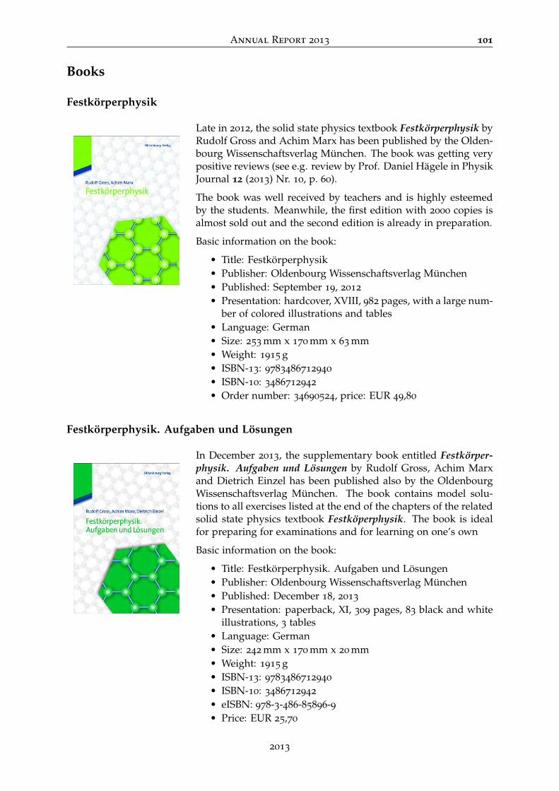
Annual Report 2013 101
Books
Festkörperphysik
Late in 2012, the solid state physics textbook Festkörperphysik byRudolf Gross and Achim Marx has been published by the Olden-bourg Wissenschaftsverlag München. The book was getting verypositive reviews (see e.g. review by Prof. Daniel Hägele in PhysikJournal 12 (2013) Nr. 10, p. 60).
The book was well received by teachers and is highly esteemedby the students. Meanwhile, the first edition with 2000 copies isalmost sold out and the second edition is already in preparation.
Basic information on the book:
• Title: Festkörperphysik• Publisher: Oldenbourg Wissenschaftsverlag München• Published: September 19, 2012
• Presentation: hardcover, XVIII, 982 pages, with a large num-ber of colored illustrations and tables
• Language: German• Size: 253 mm x 170 mm x 63 mm• Weight: 1915 g• ISBN-13: 9783486712940
• ISBN-10: 3486712942
• Order number: 34690524, price: EUR 49,80
Festkörperphysik. Aufgaben und Lösungen
In December 2013, the supplementary book entitled Festkörper-physik. Aufgaben und Lösungen by Rudolf Gross, Achim Marxand Dietrich Einzel has been published also by the OldenbourgWissenschaftsverlag München. The book contains model solu-tions to all exercises listed at the end of the chapters of the relatedsolid state physics textbook Festköperphysik. The book is idealfor preparing for examinations and for learning on one’s own
Basic information on the book:
• Title: Festkörperphysik. Aufgaben und Lösungen• Publisher: Oldenbourg Wissenschaftsverlag München• Published: December 18, 2013
• Presentation: paperback, XI, 309 pages, 83 black and whiteillustrations, 3 tables
• Language: German• Size: 242 mm x 170 mm x 20 mm• Weight: 1915 g• ISBN-13: 9783486712940
• ISBN-10: 3486712942
• eISBN: 978-3-486-85896-9• Price: EUR 25,70
2013

102 Walther–Meißner–Institut
© Walther-Meißner-Institut

Annual Report 2013 103
Theses, Appointments, Honors and Awards, Membership in Advi-sory Boards, etc.
Completed and ongoing Ph.D. Theses
Completed Ph.D. Theses:
1. Experiments on Two-Resonator Circuit Quantum Electrodynamics: A Superconduct-ing Quantum SwitchElisabeth Hoffmann, TU München, May 2013.
2. Microwave Circuit-electrodynamics in a Nanomechanical Hybrid SystemFredrik Hocke, TU München, September 2013.
3. High Magnetic Field Properties of Electron-doped Cuprate SuperconductorsToni Helm, TU München, September 2013.
4. Propagating Quantum Microwaves: Dual-path State Reconstruction and Path Entan-glementEdwin Peter Kurt Menzel, TU München, December 2013.
Ongoing Ph.D. Theses:
5. Wechselwirkung zwischen Spin-, Gitter- und Ladungsfreiheitsgraden in korreliertenMetallen ohne InversionszentrumHans-Martin Eiter, TU München, since October 2008.
6. Superconducting Flux Qubits with Tunable GapManuel Schwarz, TU München, since June 2009.
7. All Optical Quantum ComputingMax Häberlein, TU München, since December 2009.
8. Raman-Untersuchungen an stark korrelierten Systemen mit hoher OrtsauflösungFlorian Kretschmar, TU München, since January 2010.
9. Vibrational Investigations of Luminescence MoleculesNitin Chelwani, TU München, since September 2010.
10. Time-Domain Measurements on Ultra-strong-coupled Qubit-Resonator SystemsAlexander Baust, TU München, since October 2010.
11. Spinabhängige thermogalvanische Effekte in ferromagnetischen DünnschichtenJohannes Lotze, TU München, since April 2011.
12. Generation and Detection of Quantum Correlations in Circuit QED SystemsLing Zhong, TU München, since November 2011.
13. Superconducting Quantum Circuits for Qunatum Electrodynamics ExperimentsKarl Friedrich Wulschner, TU München, since January 2012.
14. Circuit Quantum Electrodynamics Experiments with Tunable Flux QubitsJan Goetz, TU München, since January 2012.
15. Single Excitation Transfer in the Quantum Regime: A Spin-Based Solid State Ap-proachChristoph Zollitsch, TU München, since January 2012.
16. Untersuchung der verschiedenen Phasen eisenbasierter Supraleiter mittels Raman-StreuungAndreas Baum, TU München, since April 2012.
17. Superconducting Properties of Organic Metals in the Vicinity of Ordering Instabili-tiesMichael Kunz, TU München, since August 2012.
2013

104 Walther–Meißner–Institut
18. Quantum Information Processing with Propagating Quantum MicrowavesPeter Eder, TU München, since November 2012.
19. Coupled Electro-Nanomechanical SystemsMatthias Pernpeintner, TU München, since November 2012.
20. Spin Transport in Ferrromagnetic MicrosturcturesMichael Schreier, TU München, since December 2012.
21. Spin dynamics and spin transport in solid state systemsHannes Maier-Flaig, TU München, since November 2013.
22. Circuit Quantum Electrodynamics with Three-dimensional CavitiesEdwar Xie, TU München, since December 2013.
The following Ph.D. students of the Walther-Meißner-Institute have finished their Ph.D. thesesin 2013:
Toni Helm
Elisabeth HoffmannEdwin Menzel
Fredrik Hocke
© Walther-Meißner-Institut

Annual Report 2013 105
Completed and ongoing Diploma, Bachelor, Master Theses
Completed Master and Diploma Theses:
1. Optimization of Josephson Junction Nanofabrication for Superconducting QuantumCircuitsFranz Sterr, Diplomarbeit, TU München, March 2013.
2. Spin Dynamics in an AntiferromagnetMarc Philipp Ross, Diplomarbeit, TU München, March 2013.
3. Development of a Time-correlated Single Photon Counting System Based on X-rayExcitation and Temporal Characterization of Ultra-fast ScintillatorsTobias Lamm, Masterarbeit, TU München, July 2013.
4. Spin Hall Magnetoresistive NoiseFriedrich Paul Witek, Masterarbeit, TU München, August 2013.
5. Magnetic properties of high quality single crystals of the electron underdoped cupratesuperconductor Nd2−xCexCuO4+δ
Alma Gabriela Dorantes Palacios, LMU München, October 2013.6. Ferroic Emitter Devices for Spin Polarized Electron Emission
Stefan Hohenberger, Masterarbeit, Joint International Graduate Program Advanced Ma-terials Science, TU München/LMU München/Universität Augsburg, November 2013.
7. Optimized Fabrication Process for Nanoscale Josephson Junctions Used in Supercon-ducting Quantum CircuitsEdwar Xie, Masterarbeit, TU München, November 2012.
8. Design and Characterization of a Superconducting Beam Splitter for Quantum Infor-mation ProcessingFerdinand Loacker, Diplomarbeit, TU München, Dezember 2013.
Completed Bachelor Theses:
9. Organic superconductor as a low-temperature pressure gaugeIsmail Achmed-Zade, Bachelor-Thesis, TU München, 2013.
10. Impedanzangepasste Widerstandsmessungen bei Frequenzen im Gigahertz-BereichKorbinian Baumgärtl, Bachelor-Thesis, TU München, 2013.
11. Vector Modulation of Microwaves for Circuit QED ExperimentsStefan Gantner, Bachelor-Thesis, TU München, 2013.
12. Gap suppression in superconducting cylinders: analytic results from the Ginzburg-Landau theoryLuzia Höhlein, Bachelor-Thesis, TU München, 2013.
13. Spin Hall-Magnetoresistance in FMI/NM/FMI-TrilayersDominik Irber, Bachelor-Thesis, TU München, 2013.
14. Charakterisierung nanomechanischer Balken mittels optischer InterferometrieMoritz Jung, Bachelor-Thesis, TU München, 2013.
15. Torque Magnetometry With Quartz Tuning ForksStefan Klimesch, Bachelor-Thesis, TU München, 2013.
16. Nd2Ir2O7: Ein neues Weyl-Halbmetall?Michaela Renate Lammel, Bachelor-Thesis, TU München, 2013.
17. Atomic Force Microscopy on Nano-Scale Josephson ContactsDominik Martin Müller, Bachelor-Thesis, TU München, 2013.
18. Interference Effects on Superconducting Coplanar Waveguide StructuresHans Gürtner, Bachelor-Thesis, TU München, 2013.
2013
106 Walther–Meißner–Institut
19. Fabrication and Characterization of Y3Fe5O12/Pt/Y3Fe5O12 Trilayers for Spin CurrentBased ExperimentsFelix Schade, Bachelor-Thesis, TU München, 2013.
20. Fast-Fourier-Transform-Based Electrical Noise MeasurementsAlexander Schade, Bachelor-Thesis, TU München, 2013.
21. Hall Effect Measurements in YIG/Pt HybridsRichard Schlitz, Bachelor-Thesis, TU München, 2013.
22. Herstellung und Charakterisierung von Y3Fe5O12-Pt Bilagen für Spinstrom basierteExperimenteMarc Schneider, Bachelor-Thesis, TU München, 2013.
23. Joule Heating Induced Spin-Seebeck EffectErich Dobler, Bachelor-Thesis, TU München, 2013.
24. Starke Kopplung in Hybridsystemen aus einem Ferrimagnet und einem supraleiten-den MikrowellenresonatorChristian Vogl, Bachelor-Thesis, TU München, 2013.
25. Spitzenverstärkte Raman-Streuung (TERS)Roland Richter, Bachelor-Thesis, TU München, 2013.
26. Phononen in entzwillingtem BaFe2As2Daniel Jost, Bachelor-Thesis, TU München, 2013.
27. Untersuchung von BaFe2As2 unter dem Einfluss von uniaxialem DruckAli Özkü, Bachelor-Thesis, TU München, 2013.
Ongoing Master and Diploma Theses:
28. SpinkaloritronikMathias Frank, Masterarbeit, TU München, since November 2012.
29. High-field Normal State Magnetotransport Properties of Electron Doped Cuprate Su-perconductorsVassilios Tzanos, Masterarbeit, TU München, since March 2013.
30. NanomechanikRasmus Holländer, TU München, since March 2013.
31. Time-resolved Spin-Seebeck EffectNiklas Roschewsky, Masterarbeit, TU München, since March 2013.
32. Magnetoelektrische Effekte in multifunktionalen SchichtstrukturenBastian Stibbe, Diplomarbeit, TU München, since May 2013.
33. Bestimmung thermischer Materialparameter an Dünnschicht-SolarzellenValentin Kunkel, Masterarbeit, TU München, since June 2013.
34. Untersuchung der konkurrierenden Phasen in unkonventionellen SupraleitungAndreas Walter, Masterarbeit, TU München, since October 2013.
35. Topological Phases in Pyroclore IridatesAndreas Wörfel, Masterarbeit, TU München, since October 2013.
36. Thin Film Fabrication for Spin Current and Spin Caloritronic ExperimentsFrancesco Della Colletta, Masterarbeit, TU München, since October 2013.
37. Magnetotransport Studies of Organic Superconductors Containing Paramagnetic IonsLudwig Schaidhammer, Masterarbeit, TU München, since November 2013.
38. Tunable Beam Splitter: Time Domain MeasurementsFabian Kössel, Masterarbeit, TU München, since November 2013.
39. Engineering the State of Light Using Gradiometric Flux Qubits with Tunable-GapPhilipp Summer, Masterarbeit, TU München, since November 2013.
© Walther-Meißner-Institut

Annual Report 2013 107
40. Control of the Phonon Population in Nano-electromechanical Hybrid SystemsAnh Tu Bohn, Masterarbeit, TU München, since November 2013.
41. Coherent Manipulation of Phosphorus Donor Spins in Silicon at Low TemperaturesKai Müller, Masterarbeit, TU München, since November 2013.
42. Spin-dependent Electronic Transport in Yttrium iron garnetRoland Rösslhuber, Masterarbeit, TU München, since November 2013.
43. Chains of Tunable and Nonlinear Superconducting ResonatorsUdo Schaumburger, Masterarbeit, TU München, since December 2013.
44. On-chip Quantum Beam-Splitter and Microwave InterferometerMichael Fischer, Masterarbeit, TU München, since December 2013.
2013

108 Walther–Meißner–Institut
© Walther-Meißner-Institut
Annual Report 2013 109
Research Projects and Cooperations
A large number of our research projects are benefiting from the collaboration with externalgroups in joint research projects, as well as from individual collaborations, exchange programsand visitors. Most collaborations are based on joint projects, which are funded by differentresearch organizations (see list below). A considerable number of collaborations also existswith universities, other research institutions and industry without direct financial support.
Funded Projects
A. German Research Foundation: Excellence Initiative
Cluster of Excellence “Nanosystems Initiative Munich”
1. Project Area I: Quantum NanophysicsF. Deppe, S.T.B. Gönnenwein, R. Gross, H. Huebl, A. Marx
2. Project Area II: Hybrid NanosystemsS.T.B. Gönnenwein, R. Gross, H. Huebl
B. German Research Foundation: Collaborative Research Centers
Collaborative Research Center 631: “Solid-State Quantum Information Processing: Physical Con-cepts and Materials Aspects”
1. Project A3: Superconducting Quantum Circuits as Basic Elements for Quantum InformationProcessingR. Gross, A. Marx
2. Project A8: Cavity Quantum Electrodynamics with Superconducting DevicesA. Marx, R. Gross
3. Project C3: Fundamentals of Quantum Logic Gates in SiliconM. Brandt, H. Huebl, M. Stutzmann
4. Project S: Coordination of the Collaborative Research CenterR. Gross
Transregional Collaborative Research Center TRR 80: “From Electronic Correlations to Func-tionality”
1. Project A2: Spatially and Momentum Resolved Raman Studies of Correlated SystemsR. Hackl
C. German Research Foundation: Priority Programs
1. Spin-dependent thermo-galvanic effects: experimentwithin the DFG Priority Program 1538 Spin-Caloric Transport – SpinCATS.T.B. Gönnenwein, R. Gross (Az. GO 944/4-1)
2. Project: Raman study of electron dynamics and phase transitions in iron-pnictide compoundswithin the DFG Priority Program 1458 “High-Temperature Superconductivity in Iron-Pnictides”R. Hackl, R. Gross, B. Büchner, D. Johrendt, C. Honerkamp (Az. HA 2071/7-1, HA2071/7-2)
2013

110 Walther–Meißner–Institut
3. Project: Spin injection, spin transport and controllable ferromagnetism in transition metal dopedZnOwithin the DFG Priority Program 1285 “Halbleiter-Spinelektronik”R. Gross, S.T.B. Gönnenwein, M. Opel (Az. GR 1132/14-1, GR 1132/14-2, GR 1132/14-3)
D. German Research Foundation: Research Projects
1. Project: Exotic Superconductivity in Strongly Anisotropic Correlated Organic Metals in theVicinity of Insulating PhasesM. Kartsovnik, W. Biberacher, R. Gross (Az. KA 1652/4-1)
2. Project: Doping Dependent Evolution of the Fermi Surface and Competing Ordering Phenomenain Superconducting CupratesR. Gross, M. Kartsovnik, A. Erb (Az. GR 1132/15-1)
3. Project: Interaction Between Spin, Lattice, and Charge in Non-Centrosymmetric CorrelatedMetalsR. Hackl, R. Gross (Az. HA 2071/5-1)
E. European Union
1. EU Collaborative Project (call identifier FP7-ICT-2011-C), project title Quantum Propagat-ing Microwaves in Strongly Coupled Environments – PROMISCEF. Deppe, A. Marx, R. Gross, Grant Agreement no. 284566
partners: several European Universities and research facilities.2. Marie Curie Network for Initial Training (call identifier FP7-PEOPLE-2010-ITN), project
title Circuit and Cavity Quantum Electrodynamics (CCQED)R. Gross, A. Marx, F. Deppe, Grant Agreement No. PITN-GA-2010-264666
partners: several European Universities and research facilities.3. Marie Curie Network for Initial Training (call identifier FP7-PEOPLE-2009-ITN), project
title Cavity-confined Luminophores for Advanced Photonic Materials: A Training Action forYoung Researchers (FINELUMEN)R. Hackl, Grant Agreement Number PITN-GA-2008-215399
partners: several European Universities and research facilities.
F. Bavaria California Technology Center (BaCaTeC)
1. Project: Nematic Order and New Phases in Quantum MaterialsR. Hackl,partners: Profs. Thomas Devereaux, Steve Kivelson, and Sri Raghu (Stanford University)
G. German Academic Exchange Service
1. Project-based Personnel Exchange Programme (PPP) with Serbia (project 56267076: Fe-based superconductors), collaboration with the Institute of Physics, University of Bel-grade (Dr. Z.V. Popovic)R. Hackl
H. Others
© Walther-Meißner-Institut

Annual Report 2013 111
Conferences and Workshops
The Walther-Meißner-Institute has organized/co-organized the following conferences, work-shops and symposia in 2013:
International Conference on Resonator QED(September 09–13, 2013, Munich, Germany)
The conference was organized bythe EU Marie Curie Network CC-QED. It took place at the KardinalWendel Haus (Mandlstraße 23, 80802
München) close to the English Gar-den in Munich-Schwabing. It was fo-cussing on the following topics: (i) Sin-gle atom cavity QED, (ii) Multi-atomcavity QED, (iii) Circuit QED, (iv) Pho-tonic crystal cavity QED, (v) Quantuminformation processing with CCQEDsystems, (vi) Cavity optomechanics,(vii) Hybrid circuit or cavity QED sys-tems, (viii) QED without cavity. Withmore than 140 participants from allover the world, the conference was amajor and very successful event. Thefinal programme comprised 6 tutorials,28 invited talks, 18 contributed talksand 57 posters. The local CCQED net-work partners (Max-Planck-Institutefor Quantum Optics and Walther-Meißner-Institute) opened doors for atour through their laboratories. More-over, the CCQED industry partners in-vited conference attendees to visit theirfacilities or offer to meet their experts.
To disseminate research on quantumoptics and circuit QED to a broaderpublic, CCQED organized an eveningwith a public lecture by Nobel lau-reate in physics, Serge Haroche on11
th September at the Ehrensaal of theDeutsches Museum. Subsequently, apanel discussion (presented by JeanneRubner, Bayerischer Rundfunk) on“Research & Innovation” with guestsfrom research, politics and industry ex-amined the link between basic researchand innovation. The event attractedmore than 150 participants.
2013

112 Walther–Meißner–Institut
510. Wilhelm und Else Heraeus-Seminar “Non-Magnetic Control of Spin – Funda-mental Physics and Materials Design”(January 07 – 09, 2013, Bad Honnef, Germany)
The 510. WEH-Seminar was co-organized by Sebastian Gönnenwein (Walther-Meißner-Institut), Christian Heiliger (Universität Gießen), and Diemo Ködderitzsch (LMU München).
Magnetic materials playan important role in to-day’s high tech devices,for example in hard diskdrives, in magnetic sen-sors, or in magnetic actua-tors. Hereby, the magneticproperties are usually con-trolled or adjusted via the
application of external magnetic fields. While this conventional magnetic-field control ofmagnetism approach is very natural and straightforward, it suffers from severe drawbacks. Inparticular, it is difficult to locally generate the required magnetic fields, such that the magnetic-field control of magnetism can not be scaled to modern, nm-scale devices.
In recent years, alternative schemes enabling a control of magnetic moments or spins bymeans of non-magnetic control parameters have emerged. These non-magnetic control ofspin schemes take advantage, e.g., of electric fields, magneto-electric coupling, elastic strains,or thermal gradients the manipulate the magnetic properties. The corresponding multifunc-tional structures (comprising constituents with both magnetic as well as a non-magnetic func-tionality) offer intriguing new physics and material science insights and challenges.
The key intention of the 510. WEH-Seminar was to address and compare the main non-magnetic control of spin schemes currently investigated, and to discuss possible extensionsor new concepts. In addition to the fundamental physics and theoretical concepts underlyingthe different approaches, materials and device considerations will play an important role. Theseminar gave an overview over the rapidly developing field of non-magnetic spin control,while providing ample time for discussions and scientific networking.
Symposium on “Strong Coupling in Solid State Quantum Systems”, Spring Meet-ing of the Condensed Matter Section of the German Physical Society(March 10 – 14, 2013, Regensburg, Germany)
Regensburg 2013 - wissenschaftliches Programm
Bereiche I Tage I Auswahl I Suche I Aktualisierungen I Downloads I Hilfe
SYSC: Symposium Strong Coupling in Solid State Quantum Systems
SYSC 1: Strong Coupling in Solid State Quantum Systems (SYSC)
Dienstag, 12. März 2013, 09:30-12:00, H1
Hans Hübl and SebastianGönnenwein of WMI orga-nized a highly successfulsymposium on Strong Cou-pling in Solid State QuantumSystems within the SpringMeeting of the CondensedMatter Section of the Ger-man Physical Society.
© Walther-Meißner-Institut
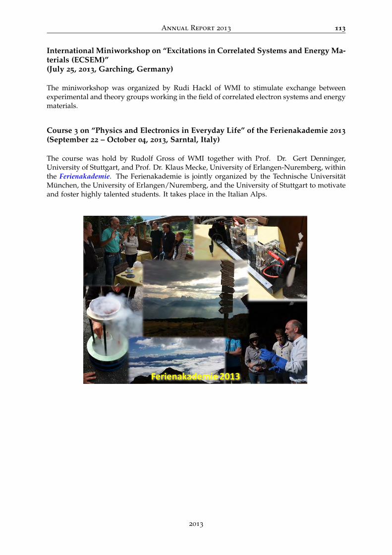
Annual Report 2013 113
International Miniworkshop on “Excitations in Correlated Systems and Energy Ma-terials (ECSEM)”(July 25, 2013, Garching, Germany)
The miniworkshop was organized by Rudi Hackl of WMI to stimulate exchange betweenexperimental and theory groups working in the field of correlated electron systems and energymaterials.
Course 3 on “Physics and Electronics in Everyday Life” of the Ferienakademie 2013(September 22 – October 04, 2013, Sarntal, Italy)
The course was hold by Rudolf Gross of WMI together with Prof. Dr. Gert Denninger,University of Stuttgart, and Prof. Dr. Klaus Mecke, University of Erlangen-Nuremberg, withinthe Ferienakademie. The Ferienakademie is jointly organized by the Technische UniversitätMünchen, the University of Erlangen/Nuremberg, and the University of Stuttgart to motivateand foster highly talented students. It takes place in the Italian Alps.
Ferienakademie 2013
2013

114 Walther–Meißner–Institut
Collaborations
Other collaborations without direct project funding involve:
• Stanford University, Stanford, USA (T.P. Devereaux, M. Greven, Z.-X. Shen, I. Fisher, B.Moritz)
• Universidad del País Vasco and Ikerbasque Foundation, Bilbao, Spain (E. Solano)• Instituto de Fisica Fundamental, Madrid, Spain (Prof. Dr. J.J. Garcia-Ripoll)• Central Research Institute of the Electric Power Industry, Tokyo, Japan (Dr. S. Ono, Dr.
Y. Ando)• Green Innovation Research Laboratories, NEC Corporation, Japan (Y. Nakamura, J.S.
Tsai, K. Inomata, T. Yamamoto)• University of Tohoku, Sendai, Japan (Gerrit E.W. Bauer, Eiji Saitoh)• European Synchrotron Radiation Facility (ESRF), Grenoble (H. Müller, D. Mannix, F.
Wilhelm, K. Ollefs)• Materials Science Research Centre, IIT Madras, India (M.S. Ramachandra Rao)• Raja Ramanna Centre for Advanced Technology, Indore, India (Lalit M. Kukreja)• ETH-Zurich, Switzerland (A. Wallraff, L. Degiorgi, R. Monnier, Dr. M. Lavagnini)• Chalmers University of Technology Gothenburg, Sweden (P. Delsing)• MINT Center, University of Alabama (A. Gupta)• Materials Physics Laboratory, Helsinki University of Technology, Finland (T. Heikkilä)• Kavli Institute of NanoScience, Delft University of Technology, Delft, The Netherlands
(T.M. Klapwijk, G.E.W. Bauer)• High-Magnetic-Field Laboratory, Grenoble, France (I. Sheikin)• High Magnetic Field Laboratory, Toulouse (C. Proust, D. Vignolles)• B. Verkin Institute for Low Temperature Research and Engineering, Kharkov, Ukraine
(V.G. Peschansky)• Landau Institute for Theoretical Physics, Chernogolovka, Russia (P. Grigoriev)• Clarendon Laboratory, University of Oxford, England (A. Karenowska)• Russian Academy of Sciences, Chernogolovka, Russia (N. Kushch, A. Palnichenko)• High Magnetic Field Laboratory, Dresden (E. Kampert, J. Wosnitza)• National High Magnetic Field Laboratory, Tallahassee, USA (J. Brooks)• University of Bonn, Germany (Prof. Dr. W. Mader)• IFW Dresden, Germany (B. Büchner, J. Fink, S.V. Borisenko, M. Knupfer)• Max-Planck-Institut für Festkörperforschung, Stuttgart (B. Keimer, L. Boeri)• University of Tübingen, Germany (R. Kleiner, D. Kölle)• University of Würzburg, Germany (W. Hanke, F. Assaad, C. Honerkamp, M. Potthoff)• University of Augsburg, Germany (P. Hänggi, A. Wixforth, A. Kampf, A. Loidl, J. Deisen-
hofer, V. Tsurkan)• University of Hamburg, Germany (G. Meier, W. Wurth)• University of Leipzig, Germany (J. Haase)• Abt. Halbleiterphysik, University of Ulm, Germany (W. Limmer)• RWTH Aachen, Germany (G. Güntherodt, B. Beschoten)• Georg-August-Universität, Göttingen, Germany (M. Münzenberg)• Institut für Experimentelle und Angewandte Physik, Universität Regensburg, Germany
© Walther-Meißner-Institut

Annual Report 2013 115
(Christian Back, Georg Woltersdorf)• Universität Bielefeld, Germany (G. Reiss, A. Thomas)• University of British Columbia, Vancouver, Canada (D. Bonn, A. Damascelli)• Technische Universität München, Physics Department, Germany (D. Grundler, Ch. Pflei-
derer, F.C. Simmel, Jean Come Lanfranchi)• Walter Schottky Institut, TU München, Germany (G. Abstreiter, M. Stutzmann, J. Finley,
M. Brandt, A. Holleitner)• Ludwig-Maximilians-Universität München, Physics Department, Germany (J.P. Kot-
thaus, J. von Delft, E. Frey, J. Rädler, S. Ludwig)• Ludwig-Maximilians-Universität München, Chemistry Department, Germany (Hubert
Ebert, Diemo Ködderitzsch)• Departamento de Fisica de la Materia Condensada, Universidad de Zaragoza, Spain (L.
Morellon, J.M. de Teresa, D. Zueco)• EPFL Lausanne, Switzerland (T. Kippenberg, H. Ronnov)• University of New South Wales, Sydney, Australia (M. Simmons, A. Morello)• McMaster University, Hamilton, Canada (J.P. Carbotte)• Technische Universität Graz, Austria (E. Schachinger)• Universität Konstanz (A. Leitenstorfer, E. Weig, J. Demsar, A. Pashkin)• BMW Group, Munich, Germany (J. Schnagl)• Siemens AG, CT MM 2, Munich, Germany (R. Matz, W. Metzger)• Attocube, Munich, Germany (K. Karrai, D. Andres, E. Hoffmann)• THEVA Dünnschichttechnik, Ismaning, Germany (W. Prusseit)• Institut für Halbleiter- und Festkörperphysik, Johannes-Kepler-Universität Linz, Austria
(A. Ney)• Lehrstuhl für Technische Elektronik, Technische Universität München (M. Becherer)• Institut für Angewandte Photophysik, Technische Universität Dresden (L. Eng, D. Köh-
ler, J. Becherer)• Jülich Centre for Neutron Science JCNS (S. Pütter)• Université de Toulouse, Laboratoire de Physique Théorique, Toulouse, France (R. Ra-
mazashvili)• Lawrence Berkeley National Laboratory, Berkeley, USA (A. F. Kemper)• University of Belgrade, Belgrade, Serbia (Z. Popovic, N. Lazarevic, D. Tanaskovic)• University of Aveiro, Portugal (N. A. Sobolev)• Macquarie University, MQ Research Centre for Quantum Science and Technology, Aus-
tralia (J. Twamley)• Instituto de Ciencia de Materiales de Sevilla, Spain (J. Poyato, J.L. Perez-Rodriguez)• Research Institute for Solid State Physics and Optics, Hungarian Academy of Sciences,
Budapest, Hungary (K. Kamaras, I. Tüttö, J. Balogh)• University of Rome “La Sapienza”, Rome, Italy (S. Caprara, C. Di Castro, M. Grilli)• Hungarian Academy of Sciences, Budapest University of Technology and Economics,
Budapest, Hungary (A. Virosztek, A. Zawadowski, G. Mihály)
2013
116 Walther–Meißner–Institut
Stays abroad
Extended visits of members of the Walther-Meißner-Institute at foreign research laboratories:
1. Rudi HacklStanford University and Stanford Institute for Materials and Energy Science, Stanford,USA24. 03. - 12. 04. 2013, 19. 06. - 03. 07. 2013
2. Toni HelmHigh Magnetic Field Laboratory, Toulouse, France07. 04. - 12. 04. 2013
3. Toni HelmHigh Magnetic Field Laboratory, Dresden, Germany29. 08. - 07. 09. 2013
4. Mark Kartsovnik, Toni Helm, Vasilis TzanosHigh Magnetic Field Laboratory, Grenoble, France20. 04. - 29. 04. 2013
5. Mark KartsovnikHigh Magnetic Field Laboratory, Grenoble, France08. 10. - 16. 10. 2013
6. Vasilis TzanosHigh Magnetic Field Laboratory, Grenoble, France18. 08. - 26. 08. 2013
7. Alexander BaustNEC Corporation, Smart Energy Research Laboratories, Tsukuba, Ibaraki, Japan19. 08. - 18. 10. 2013
© Walther-Meißner-Institut
Annual Report 2013 117
Conference Talks and Seminar Lectures
Andreas Baum
1. Phonons in twin-free BaFe2As2International Miniworkshop on “Excitations in Correlated Systems and Energy Materials (EC-SEM)” Walther-Meißner-Institut, Garching, Germany.25. 07. 2013
2. Lattice dynamics in detwinned BaFe2As2 as observed via Raman scatteringSpring Meeting of the DPG, Regensburg, Germany.12. 03. 2013
Alexander Baust
1. Tunable Coupling between Two Resonators Controlled by a Flux Qubit: the Quantum SwitchSpring Meeting of the DPG, Regensburg, Germany.13. 03. 2013
2. Tunable Coupling between Two Resonators Controlled by a Flux Qubit: the Quantum SwitchAPS March Meeting, Baltimore, USA.21. 03. 2013
Thomas Böhm
1. Band structure and superconductivity in Ba1−xKxFe2As2International Miniworkshop on “Excitations in Correlated Systems and Energy Materials (EC-SEM)”, Walther-Meißner-Institut, Garching, Germany.25. 07. 2013
2. Superconducting gaps and collective mode in Ba0.6K0.4Fe2As2 as detected in Raman spec-troscopyStanford Institute for Materials and Energy Science, Stanford National Accelerator Laboratory,Stanford, USA.13. 05. 2013
3. Subdominant d-wave pairing in BKFAInstitute of Physics, University of Belgrade, Belgrade, Serbia.10. – 14. 12. 2013
Nitin Chelwani
1. Progress report on tip-enhanced Raman scatteringInternational Miniworkshop on “Excitations in Correlated Systems and Energy Materials (EC-SEM)”, Walther-Meißner-Institut, Garching, Germany.25. 07. 2013
Frank Deppe
1. From squeezed microwave light to path entanglementInvited talk, Conference on Resonator QED, Munich, Germany.09. – 13. 09. 2013
2. Tunable and switchable coupling between two superconducting transmission line resonatorsInvited talk, NIM Workshop “Young Ideas in Nanoscience”, Munich, Germany-19. – 20. 11. 2013
Hans-Martin Eiter
1. Helical magnetic order in MnSiInternational Miniworkshop on “Excitations in Correlated Systems and Energy Materials (EC-SEM)”, Walther-Meißner-Institut, Garching, Germany-25. 07. 2013
Andreas Erb
1. Crystal growth of superconducting and magnetically ordering oxides using the TSFZ tech-nique
2013
118 Walther–Meißner–Institut
Workshop on “Floating Zone Technique”, Leibniz Institute for Solid State and Materials ResearchDresden, Germany.20. - 22. 02. 2013
2. Growth of High-Purity CaWO4 Single Crystals for the Low-Temperature Dark Matter Re-search Experiments CRESST and EURECACollaborative Conference on Crystal Growth (3CG), Cancun, Mexico.10. – 13. 06. 2013
3. Crystal Growth of various Oxides using the TSFZ TechnigueDGKK-Arbeitskreis-Treffen “Intermetallische und oxidische Systeme mit Spin und Ladungskor-relationen”, Vienna, Austria.26. – 27. 09. 2013
4. Single crystal growth of various oxide materials for basic research and applicationsPhysik-Kolloquium, Universität Leipzig, Germany.10. 12. 2013
Stephan Geprägs1. Magnetoelastic and Magnetoelectric Effects in Extrinsic Multiferroic Hybrid Structures
510. WE-Heraeus-Seminar, Bad Honnef, Germany.06. – 09. 01. 2013
Sebastian Gönnenwein1. Spin Currents in Magneto-Thermal Landscapes
12th Joint Intermag/MMM Conference, Chicago, USA-17. 01. 2013
2. Spin Currents in Magneto-Thermal LandscapesTrends in Nanoscience 2013, Kloster Irsee, Irsee, Germany-27. 02. 2013
3. Spin Mechanics in Ferromagnet/Ferroelectric Hybrid StructuresMarch Meeting of the American Physical Society, Baltimore, USA-20. 03. 2013
4. Spin Current-Based Experiments in Ferromagnet/Normal Metal HybridsSeminarvortrag im SFB-Kolloquium, Universität Hamburg, Germany07. 05. 2013
5. Experimental Test of the Spin Mixing Interface Conductivity ConceptSpin Caloritronics V, Columbus, USA.23. 05. 2013
6. Spin Currents in Ferromagnet/Normal Metal HybridsQuantum NanoScience Seminar, TU Delft, The Netherlands.26. 06. 2013
7. Spin Seebeck ExperimentsGordon Research Conference on Spin Dynamics in Nanostructures, Hong Kong, China.18. 08. 2013
8. Charge and Spin Currents in Hybrid StructuresThe Kavli Institute for Theoretical Physics Program Sprintronics: Progress in Theory, Materialsand Devices, UC Santa Barbara, USA.10. 10. 2013
9. Spin Currents in Ferromagnet/Normal Metal Hybrid StructuresPhysik-Kolloquium, Universität Dortmund, Germany.12. 11. 2013
10. Spin Currents in Ferromagnet/Normal Metal Hybrid StructuresSeminar of the Institute of Condensed Matter, École Polytechnique Féderale de Lausanne,Switzerland.27. 11. 2013
Jan Goetz1. Tunable gradiometric flux qubits in circuit-QED experiments
Spring Meeting of the DPG, Regensburg, Germany.10. - 15. 03. 2013
© Walther-Meißner-Institut
Annual Report 2013 119
Rudolf Gross
1. Quantum X-tronics: From Quantifiable to QuantumR. Gross24. Edgar-Lüscher-Seminar, “Neues aus der Festkörperphysik”02 – 08 February, 2013, Klosters, Switzerland.
2. Fermi Surfaces in Electron-Doped Cuprate SuperconductorsR. GrossInvited Talk, Workshop on “Strongly Correlated Transition Metal Compounds”06 – 08 March, 2013, Cologne, Germany.
3. Hochtemperatur-SupraleitungR. GrossInvited Tutorial, 37. Edgar-Lüscher Physikseminar über “Zukunftsmaterialien”12 – 14 April, 2013, Zwiesel, Germany.
4. Quantum Spin Physics with Magnetic NanostructuresR. Gross15. 05. 2013
Kolloquium der Fakultät für Physik, Universität Duisburg-Essen, Germany.5. Exploring the Quantum with Superconducting Circuits
R. GrossInvited Talk, 4. International Conference on Quantum Metrology15 – 17 May, 2013, Poznan, Poland.
6. Exploring the Quantum with Superconducting CircuitsR. Gross25. 06. 2013
Großes Physikalisches Kolloquium, Universität zu Köln, Germany.7. Exploring Pure Spin Currents and Quantum Spin Physics
R. GrossPlenary Talk, International Conference on Nanoscale Magnetism (ICNM-2013)02 – 06 September, 2013, Istanbul, Turkey.
8. Nano- und QuantensystemeR. Gross19. 10. 2013
Public Lecture, Day of Open House, Garching, Germany.9. Superconducting Quantum Hybrid Systems
R. GrossInvited Talk, 545. WE-Heraeus-Seminar “Superconducting Proximity and Josephson Effects inNanoscale Systems”19 – 22 November, 2013, Bad Honnef, Germany.
10. Physics with Pure Spin CurrentsR. Gross10. 12. 2013
Colloquium of the Indian Institute of Technology Madras, Chennai, India.11. Semiconductor-Superconductor Hybrids for Circuit Nano-Electromechanics
R. GrossInvited Talk, 17
th International Workshop on “The Physics of Semiconductor Devices”10 – 13 December, 2013, Amity University, Uttar Pradesh, India.
12. Circuit Nano-ElectromechanicsR. GrossPlenary Talk, International Conference of the International Union of Materials Research Societies,IUMRS-ICA 2013
16 – 20 December, 2013, Bangalore, India.
Rudolf Hackl
1. A light scattering study of the evolution of pairing in Fe-based superconductorsSpring Meeting of the DPG, Regensburg, Germany14. 03. 2013
2013

120 Walther–Meißner–Institut
2. Charge density wave formation in multiband systemsAPS March Meeting, Baltimore, USA22. 03. 2013
3. Collective Excitations in Superconductors and Density Wave SystemsColloquium at the Stanford Institute for Materials and Energy Science, Stanford National Accel-erator Laboratory, Stanford, USA.29. 03. 2013
4. Fermi surface topology and superconductivity in Fe-based materialsInternational Conference on SQuantum in Complex Matter - SuperstripesT, Ischia, Italy.30. 05. 2013
5. Spectroscopic evidence of coherence phenomena in superconductorsInvited talk at the 6th internal biennial science meeting of the MLZ, Grainau, Germany.12. 06. 2013
6. Raman scattering experiments on gap and collective excitations in Fe-based superconductorsInvited talk, International Conference on Spectroscopic in Novel Superconductors (SNS 2013),Berkeley, USA.28. 06. 2013
7. Raman scattering in high-Tc superconductorsFestkolloquium on the occasion of the 70th birthday of Werner Hanke and inauguration of theWilly Wien Center, Würzburg, Germany.19. 07. 2013
8. Light scattering experiments in diamond anvil cellsMLZ Garching, Germany.10. 12. 2013
9. Electronic Raman scattering and the CDW in RTe3Institute of Physics, University of Belgrade, Belgrade, Serbia.10. – 14. 12. 2013
Toni Helm1. High-field magnetotransport in electron doped High-Tc Superconductors
Lawrence Berkeley National Laboratory, Berkeley, USA.26. 04. 2013
2. Correlations between superconductivity and symmetry-breaking instabilities in the n-dopedcuprate Nd2−xCexCuO4 probed by high-field magnetotransportEMFL User Meeting, Nijmegen, The Netherlands.12. – 13. 06. 2013
Hans Hübl1. Coupling Phosphorus Donors and Microwave Resonators
Silicon Quantum Electronics, Grenoble, France.07. – 08. 02. 2013
2. Two-tone experiments and time domain control in circuit nano-electromechanics high coop-erativity in coupled microwave resonator – ferromagnetic insulator hybridsAPS Spring Meeting, Baltimore, USA.18. – 22. 03. 2013
3. Two-tone experiments and time domain control in circuit nano-electromechanicsSpring Meeting of the DPG, Regensburg, Germany.10. – 15. 03. 2013
4. High cooperativity in coupled microwave resonator – ferromagnetic insulator hybridsGRC Spin Dynamics in Nanostructures, Hong Kong, China.18. – 23. 08. 2013
5. Nano-Opto-Mechnics at Microwave FrequenciesInvited talk, Young Ideas in Nanoscience (NIM), Munich, Germany.19. – 20. 11. 2013
Mark Kartsovnik1. Correlation between Fermi surface transformations and superconductivity in an electron-
doped high-Tc superconductors
© Walther-Meißner-Institut

Annual Report 2013 121
Invited talk, International Conference on “Quantum in Complex Matter”, Superstripes 2013, Is-chia, Italy.27. 05. – 01. 06. 2013
2. Molecular organic metals: a playground for electronic interactions and instabilitiesInvited talk, International Symposium “NANO-2013, Knowledge Society: mutual influence andinterference of science and society”, Chisinau, Moldova.13. – 16. 09. 2013
Florian Kretzschmar
1. Fluctuations and spin density wave (SDW) order in BaFe2As2International Miniworkshop on “Excitations in Correlated Systems and Energy Materials (EC-SEM)”, Walther-Meißner-Institut, Garching, Germany.25. 07. 2013
2. Evidence of competing s and d-wave pairing channels in iron-based superconductorsAPS March Meeting, Baltimore, USA.21. 03. 2013
3. Evidence of competing s and d-wave pairing channels in iron-based superconductorsStanford Institute for Materials and Energy Science, Stanford National Accelerator Laboratory,Stanford, USA.28. 03. 2013
Edwin Menzel
1. Entanglement of Continuous-Variable Quantum MicrowaveSpring Meeting of the DPG, Regensburg, Germany.10. - 15. 03. 2013
Matthias Opel
1. Spin Transport and Spin Dephasing in Zinc OxideSpring Meeting of the DPG, Regensburg, Germany.11. 03. 2013
2. Absence of an induced magnetic moment in Pt on Y3Fe5O12 (YIG)Joint European Magnetic Symposia (JEMS), Rhodos, Greece.29. 08. 2013
3. Electrical Spin Transport and Spin Relaxation in Zinc OxideInternational Workshop on “Semiconductor Spintronics” & Final Meeting of the DFG PriorityProgram SPP 1285 “Halbleiter-Spintronik”, Würzburg, Germany.30. 09. 2013
Erwin Schuberth
1. YbRh2Si2 at ultra-low temperaturesTechnical University, Vienna, Austria.23. – 24. 01. 2013
Kurt Uhlig
1. Dry dilution refrigerator with He-4 precool loopCryogenic Engineering Conference 2013, Anchorage, Alaska.19. 07. 2013
2013

122 Walther–Meißner–Institut
© Walther-Meißner-Institut

Annual Report 2013 123
Appointments, Membership in Advisory Boards, etc.
1. Werner Biberacher is member of the Scientific Council of the High Magnetic Field Lab-oratory (LNCMI) Grenoble/Toulouse, France.
2. Dietrich Einzel is one of the four spokesmen of the scientific staff of the BavarianAcademy of Sciences and Humanities.
3. Sebastian Gönnenwein is associate member of the Cluster of Excellence NanosystemsInitiative Munich (NIM).
4. Rudolf Gross is member of the International Advisory Committee of the InternationalConference M2S HTSC 2015, Geneva, Switzerland.
5. Rudolf Gross is member of the International Advisory Committee of the 4th Interna-tional Conference on Superconductivity and Magnetism-ICSM2014, Antalya, Turkey.
6. Rudolf Gross is member of the Scientific Advisory Board of the Leibniz Institute forSolid-State and Materials Research, Dresden.
7. Rudolf Gross is member of the Kuratorium of the Physik Journal of the German PhysicalSociety.
8. Rudolf Gross is member of the selection committee of the Stern-Gerlach-Medal of theGerman Physical Society.
9. Rudolf Gross is deputy spokesman of the division of Low Temperature Physics of theCondensed Matter Section of the German Physical Society.
10. Rudolf Gross is spokesman of the Collaborative Research Center 631 on Solid State Quan-tum Information Processing of the German Research Foundation.
11. Rudolf Gross is member of the Executive Board of the Cluster of Excellence NanosystemsInitiative Munich (NIM) and coordinator of the Research Area 1 on Quantum Nanosystems.
12. Rudolf Gross is member of the Board of Editors of the European Physical Journal B.
13. Rudolf Hackl is deputy coordinator of the DFG Priority Program SPP 1458 on “HighTemperature Superconductivity in the Iron Pnictides”.
14. Rudolf Hackl is member of the evaluation board of the neutron source Heinz Maier-Leibnitz (FRM II).
15. Mark Kartsovnik is member of the Selection Committee of EMFL (European MagneticField Laboratories) and of the International Advisory Committee of the 10th Interna-tional Symposium on Crystalline Organic Metals Superconductors and Ferromagnets(ISCOM2013)
2013

124 Walther–Meißner–Institut
© Walther-Meißner-Institut
Annual Report 2013 125
Lectures, Seminars, Courses and other Scientific Activities
Several members of Walther-Meißner-Institute give lectures and seminars at the TechnischeUniversität München.
Lectures
Dietrich Einzel
WS 2012/2013 • Mathematische Methoden der Physik I (Mathematical Methods ofPhysics I)
• Übungen zu Mathematische Methoden der Physik I (MathematicalMethods of Physics I, Problem Sessions)
• WMI-Seminar über aktuelle Fragen der Tieftemperatur-Festkörperphysik (WMI Seminar on Current Topics of Low Tem-perature Solid-State Physics, with R. Gross, S.B.T. Gönnenwein, H.Hübl, A. Marx, M. Opel, R. Hackl)
• Seminar: Advances in Solid-State Physics (with R. Gross, M. Opel, A.Marx, S.T.B. Gönnenwein)
SS 2013 • Mathematische Methoden der Physik II (Mathematical Methods ofPhysics II)
• Übungen zu Mathematische Methoden der Physik II (MathematicalMethods of Physics II, Problem Sessions)
• WMI-Seminar über aktuelle Fragen der Tieftemperatur-Festkörperphysik (WMI Seminar on Current Topics of Low Tem-perature Solid-State Physics, with R. Gross, S.B.T. Gönnenwein, H.Hübl, A. Marx, M. Opel, R. Hackl)
• Seminar: Advances in Solid-State Physics (with R. Gross, M. Opel, A.Marx, S.T.B. Gönnenwein)
WS 2013/2014 • Mathematische Methoden der Physik I (Mathematical Methods ofPhysics I)
• Übungen zu Mathematische Methoden der Physik I (MathematicalMethods of Physics I, Problem Sessions)
• WMI-Seminar über aktuelle Fragen der Tieftemperatur-Festkörperphysik (WMI Seminar on Current Topics of Low Tem-perature Solid-State Physics, with R. Gross, S.B.T. Gönnenwein, H.Hübl, A. Marx, M. Opel, R. Hackl)
• Seminar: Advances in Solid-State Physics (with R. Gross, M. Opel, A.Marx, S.T.B. Gönnenwein)
Frank Deppe
WS 2012/2013 • Supraleitung und Tieftemperaturphysik I (Superconductivity and LowTemperature Physics I, with R. Gross)
• Übungen zu Supraleitung und Tieftemperaturphysik I (Superconduc-tivity and Low Temperature Physics I, Problem Sessions)
• Seminar: Advances in Solid-State Physics (with R. Gross, M. Opel, A.Marx, S.T.B. Gönnenwein, D. Einzel)
• Seminar: Supraleitende Quantenschaltkreise (mit R. Gross, A. Marx)(Seminar on Superconducting Quantum Circuits)
2013

126 Walther–Meißner–Institut
SS 2013 • Supraleitung und Tieftemperaturphysik II (Superconductivity andLow Temperature Physics II, with R. Gross)
• Übungen zu Supraleitung und Tieftemperaturphysik II (Superconduc-tivity and Low Temperature Physics II, Problem Sessions)
• Angewandte Supraleitung: Josephson Effekte, supraleitende Elek-tronik und supraleitende Quantenschaltkreise (Applied Superconduc-tivity: Josephson Effects, Superconducting Electronics and Supercon-ducting Quantum Circuits, with R. Gross)
• Seminar: Advances in Solid-State Physics (with R. Gross, M. Opel, A.Marx, S.T.B. Gönnenwein, D. Einzel)
• Seminar: Supraleitende Quantenschaltkreise (mit R. Gross, A. Marx)(Seminar on Superconducting Quantum Circuits)
WS 2013/2014 • Seminar: Advances in Solid-State Physics (with R. Gross, M. Opel, A.Marx, S.T.B. Gönnenwein, D. Einzel)
• Seminar: Supraleitende Quantenschaltkreise (mit R. Gross, A. Marx)(Seminar on Superconducting Quantum Circuits)
Rudolf Gross
WS 2012/2013 • Supraleitung und Tieftemperaturphysik I (Superconductivity and LowTemperature Physics I)
• Übungen zu Supraleitung und Tieftemperaturphysik I (Superconduc-tivity and Low Temperature Physics I, Problem Sessions)
• WMI-Seminar über aktuelle Fragen der Tieftemperatur-Festkörperphysik (WMI Seminar on Current Topics of Low Tem-perature Solid-State Physics, with D. Einzel, S.T.B. Gönnenwein, R.Hackl, H. Hübl, A. Marx, M. Opel)
• Seminar: Advances in Solid-State Physics (with D. Einzel, S.T.B. Gön-nenwein, R. Hackl, H. Hübl, A. Marx, M. Opel)
• Seminar: Superconducting Quantum Circuits (with F. Deppe, A. Marx)• Festkörperkolloquium (Colloquium on Solid-State Physics, with D.
Einzel)SS 2013 • Supraleitung und Tieftemperaturphysik II (Superconductivity and
Low Temperature Physics II)• Übungen zu Supraleitung und Tieftemperaturphysik II (Superconduc-
tivity and Low Temperature Physics II, Problem Sessions)• Angewandte Supraleitung: Josephson Effekte, supraleitende Elek-
tronik und supraleitende Quantenschaltkreise (Applied Superconduc-tivity: Josephson Effects, Superconducting Electronics and Supercon-ducting Quantum Circuits, with F. Deppe)
• Übungen zu Angewandte Supraleitung: Josephson Effekte, supraleit-ende Elektronik und supraleitende Quantenschaltkreise (Applied Su-perconductivity: Josephson Effects, Superconducting Electronics andSuperconducting Quantum Circuits, Problem Sessions, with F. Deppe)
• Seminar: Advances in Solid-State Physics (with D. Einzel, S.T.B. Gön-nenwein, R. Hackl, H. Hübl, A. Marx, M. Opel)
• WMI-Seminar über aktuelle Fragen der Tieftemperatur-Festkörperphysik (WMI Seminar on Current Topics of Low Tem-perature Solid-State Physics, with D. Einzel, S.T.B. Gönnenwein, R.Hackl, H. Hübl, A. Marx, M. Opel)
© Walther-Meißner-Institut

Annual Report 2013 127
• Seminar: Superconducting Quantum Circuits (with F. Deppe, A. Marx)• Festkörperkolloquium (Colloquium on Solid-State Physics, with D.
Einzel)• Ferienakademie: Kurs 3 “Physik und Elektronik im Alltag” (Ferien-
akademie: Course 3 “Physics and Electronics in Everyday Life”)WS 2013/2014 • Physik der Kondensierten Materie I (Condensed Matter Physics I)
• Übungen zu Physik der Kondensierten Materie I (Condensed MatterPhysics I, Problem Sessions, with S. Geprägs)
• WMI-Seminar über aktuelle Fragen der Tieftemperatur-Festkörperphysik (WMI Seminar on Current Topics of Low Tem-perature Solid-State Physics, with D. Einzel, S.T.B. Gönnenwein, R.Hackl, H. Hübl, A. Marx, M. Opel)
• Seminar: Advances in Solid-State Physics (with D. Einzel, S.T.B. Gön-nenwein, R. Hackl, H. Hübl, A. Marx, M. Opel)
• Seminar: Superconducting Quantum Circuits (with F. Deppe, A. Marx)• Festkörperkolloquium (Colloquium on Solid-State Physics, with D.
Einzel)
Sebastian T.B. Gönnenwein
WS 2012/2013 • Seminar: Advances in Solid-State Physics (with R. Gross, A. Marx, M.Opel)
• Magnetismus (Magnetism)• Übungen zu Magnetismus (Magnetism, Problem Sessions)• WMI-Seminar über aktuelle Fragen der Tieftemperatur-
Festkörperphysik (WMI Seminar on Current Topics of Low Tem-perature Solid State Physics, with R. Gross, D. Einzel, H. Hübl, A.Marx, M. Opel, R. Hackl)
• Seminar zu aktuellen Fragen der Magneto- und Spinelektronik (Sem-inar on Current Topics in Magneto and Spin Electronics, with M.Brandt, H. Hübl)
SS 2013 • Seminar: Advances in Solid-State Physics (with R. Gross, A. Marx, M.Opel)
• Spin Electronics• Übungen zu Spin Electronics (Exercises to Spin Electronics)• WMI-Seminar über aktuelle Fragen der Tieftemperatur-
Festkörperphysik (WMI Seminar on Current Topics of Low Tem-perature Solid State Physics, with R. Gross, D. Einzel, H. Hübl, A.Marx, M. Opel, R. Hackl)
• Seminar zu aktuellen Fragen der Magneto- und Spinelektronik (Sem-inar on Current Topics in Magneto and Spin Electronics, with M.Brandt, H. Hübl)
WS 2013/2014 • Seminar: Advances in Solid-State Physics (with R. Gross, A. Marx, M.Opel)
• Magnetismus (Magnetism)• Übungen zu Magnetismus (Magnetism, Problem Sessions)• WMI-Seminar über aktuelle Fragen der Tieftemperatur-
Festkörperphysik (WMI Seminar on Current Topics of Low Tem-perature Solid State Physics, with R. Gross, D. Einzel, H. Hübl, A.Marx, M. Opel, R. Hackl)
2013
128 Walther–Meißner–Institut
• Seminar zu aktuellen Fragen der Magneto- und Spinelektronik (Sem-inar on Current Topics in Magneto and Spin Electronics, with M.Brandt, H. Hübl)
Rudi Hackl
WS 2012/2013 • Seminar: Advances in Solid-State Physics (with R. Gross, S.T.B. Gön-nenwein, H. Hübl, A. Marx, M. Opel)
• WMI-Seminar über aktuelle Fragen der Tieftemperatur-Festkörperphysik (WMI Seminar on Current Topics of Low Tem-perature Solid-State Physics, with R. Gross, S.B.T. Gönnenwein, H.Hübl, A. Marx, M. Opel, D. Einzel)
WS 2013/2014 • Low Temperature Physics and Superconductivity I (with R. Gross)• Exercises to Low Temperature Physics and Superconductivity I• Seminar: Advances in Solid-State Physics (with R. Gross, S.T.B. Gön-
nenwein, H. Hübl, A. Marx, M. Opel)• WMI-Seminar über aktuelle Fragen der Tieftemperatur-
Festkörperphysik (WMI Seminar on Current Topics of Low Tem-perature Solid-State Physics, with R. Gross, S.B.T. Gönnenwein, H.Hübl, A. Marx, M. Opel, D. Einzel)
Hans Hübl
WS 2012/2013 • Seminar: Spin Caloritronics and Spin Pumping• Seminar: Advances in Solid-State Physics (with R. Gross, D. Einzel,
S.T.B. Gönnenwein, A. Marx, M. Opel)• WMI-Seminar über aktuelle Fragen der Tieftemperatur-
Festkörperphysik (WMI Seminar on Current Topics of Low Tempera-ture Solid State Physics, with R. Gross, D. Einzel, S.T.B. Gönnenwein,A. Marx, M. Opel, R. Hackl)
• Seminar zu aktuellen Fragen der Magneto- und Spinelektronik (Sem-inar on Current Topics in Magneto and Spin Electronics, with S.T.B.Gönnenwein, M. S. Brandt)
SS 2013 • Seminar: Spin Caloritronics and Spin Pumping• Seminar: Advances in Solid-State Physics (with R. Gross, D. Einzel,
S.T.B. Gönnenwein, A. Marx, M. Opel)• WMI-Seminar über aktuelle Fragen der Tieftemperatur-
Festkörperphysik (WMI Seminar on Current Topics of Low Tempera-ture Solid State Physics, with R. Gross, D. Einzel, S.T.B. Gönnenwein,A. Marx, M. Opel, R. Hackl)
• Seminar zu aktuellen Fragen der Magneto- und Spinelektronik (Sem-inar on Current Topics in Magneto and Spin Electronics, with S.T.B.Gönnenwein, M. S. Brandt)
WS 2013/2014 • Seminar: Spin Caloritronics and Spin Pumping• Seminar: Advances in Solid-State Physics (with R. Gross, D. Einzel,
S.T.B. Gönnenwein, A. Marx, M. Opel)• WMI-Seminar über aktuelle Fragen der Tieftemperatur-
Festkörperphysik (WMI Seminar on Current Topics of Low Tempera-ture Solid State Physics, with R. Gross, D. Einzel, S.T.B. Gönnenwein,A. Marx, M. Opel, R. Hackl)
© Walther-Meißner-Institut
Annual Report 2013 129
• Seminar zu aktuellen Fragen der Magneto- und Spinelektronik (Sem-inar on Current Topics in Magneto and Spin Electronics, with S.T.B.Gönnenwein, M. S. Brandt)
Anton Lerf
WS 2012/2013 • Moderne Aspekte der Chemie für Physiker I (Modern Aspects ofChemistry for Physicists I)
2013

130 Walther–Meißner–Institut
ïz£
The WMI Seminars
The Friday Seminar –Walther-Meißner-Seminar on Current Topics in Low Temperature Physics
WS 2012/2013:
1. Dynamics in Quantum AntiferromagnetsProf. Dr. Goetz Uhrig, Lehrstuhl für Theoretische Physik I, Technische Universität Dortmund,Germany26. 11. 2012
2. Exotic phases of matter: from critical metals to chiral magnetsProf. Dr. Markus Garst, Institut für Theoretische Physik, Universität zu Köln, Germany03. 12. 2012
3. Quantum Transport in Hybrid NanosystemsProf. Dr. Jürgen König, Fakultät für Physik, Universität Duisburg-Essen, Germany04. 12. 2012
4. A Quantum Impurity Perspective on Strongly Correlated SystemsProf. Dr. Walter Hofstetter, Institut für Theoretische Physik, Johann Wolfgang Goethe-UniversitätFrankfurt, Germany10. 12. 2012
5. Progress in Quantum Monte Carlo Simulations: recent highlights and future prospectsProf. Dr. Lode Pollet, Theoretische Nanophysik, LMU München, Germany23. 01. 2013
6. Be Entrepreneurial! Opportunities for founders at TUMHarald Jenull, UnternehmerTUM GmbH, Garching, Germany01. 02. 2013
7. Raman Scattering in Multiband SystemsDr. Elizabeth A. Nowadnick, Stanford Institute for Materials and Energy Sciences (SIMES),Stanford University, Stanford, USA08. 02. 2013
8. Giant and reversible extrinsic magnetocaloric effects in manganite films due to strainDr. Neil D. Mathur, Department of Materials Science and Metallurgy, University of Cambridge,United Kingdom18. 02. 2013
SS 2013:
9. Magnetism studies in TM-doped ZnO-based structuresProf. Dr. Nikolai Sobolev, Departamento de Fisica, Universidade De Aveiro, Portugal26. 04. 2013
10. Multiband, paramagnetic effects and vortices in KFe2As2Dr. Frédéric Hardy, Karlsruher Institut für Technologie (KIT), Karlsruhe17. 05. 2013
11. Superconducting Artificial Atom with Two Degrees of FreedomDr. Olivier Buisson, Institut Neel, CNRS & Université Joseph Fourier & INP-Grenoble, France24. 05. 2013
12. Towards a spin-ensemble quantum memory for superconducting qubitsDr. Patrice Bertet, Research Group in Quantum Electrics, Gif-sur-Yvette, France07. 06. 2013
13. Geometric phases for robust quantum gates in circuit QEDDr. Stefan Filipp, Laboratorium für Festkörperphysik, ETH Zürich, Switzerland14. 06. 2013
14. Calculating the Electronic Structure of Materials with Strong Electronic Coulomb Correla-tions from First Principles? – Where do we stand?
© Walther-Meißner-Institut

Annual Report 2013 131
Prof. Dr. Silke Biermann, Centre de Physique Théorique – UMR 7644 EPFL, Lausanne, Switzer-land21. 06. 2013
15. Fluxons for quantum circuitsDipl.-Phys. Kirill Fedorov, Karlsruhe Institute of Technology, Karlsruhe, Germany21. 06. 2013
16. Quantum corrections for low temperature electrical conductivity of SixZn1−xO thin filmsProf. Dr. Lalit Kukreja, Laser Materials Processing Division, Raja Ramanna Centre for AdvancedTechnology, Indore, India28. 06. 2013
17. Listening to the brain with high-Tc SQUIDsProf. Dr. Dag Winkler, Chalmers University of Technology, Göteborg, Sweden05. 07. 2013
18. Acoustic Microscopy as a Probe for MagnonsProf. Dr. Andrew Briggs, University of Oxford, United Kingdom10. 07. 2013
19. New Directions in Spin Current Research at NIST, BoulderProf. Dr. Tom Silva, The National Institute of Standards and Technology Boulder, Colorado, USA29. 07. 2013
20. Raman scattering study in alkali-doped transition metal selenidesDr. Nenad Lazarevic, Institute of Physics, University of Belgrade, Serbia05. 09. 2013
21. Nanomechanics in the quantum regime-from quantum optics with phonons to hybrid quan-tum systemsDr. Jörg Bochmann, University of California, Santa Barbara, USA16. 09. 2013
WS 2013/2014:
22. Single-shot readout of superconducting flux qubit using a Josephson parametric amplifierDr. Tsuyoshi Yamamoto, NEC Smart Energy Research Laboratories, NEC Corporation Tsukuba,Ibaraki, Japan16. 10. 2013
23. Hunds Metallicity in Iron-based SuperconductorsDr. Markus Aichhorn, Institute of Theoretical and Computational Physics, Technische Univer-sität Graz, Austria08. 11. 2013
24. Fine structure of the Kondo resonance in ultraclean carbon nanotube quantum dotsDr. Andreas Hüttel, Institut für Experimentelle und Angewandte Physik, Universität Regens-burg, Germany15. 11. 2013
25. Superconducting qubits: sidebands, cavities, and vorticesProf. Dr. Britton Plourde, Physics Departments, Syracuse University, Syracuse, USA22. 11. 2013
Topical Seminar on Advances in Solid State Physics –WS 2012/2013, SS 2013 and WS 2013/2014
WS 2012/2013:
1. Preliminary discussion and assignment of topicsR. Gross, Walther-Meißner-Institut16. 10. 2012, 23. 10. 2012
2. Spin Seebeck InsulatorNiklas Roschewsky, Technische Universität München20. 11. 2012
2013

132 Walther–Meißner–Institut
3. Response and collective modes in non-cetrosymmetric superconductorsNikolaj Bittner, Walther-Meißner-Institut27. 11. 2012
4. Determination of the energy gap in superconductors via scanning tunneling spectroscopyAndreas Walter, Technische Universität München04. 12. 2012
5. Quantum coherent coupling of a mechanical oscillator to an optical cavity modeMarco Bobinger, Technische Universität München11. 12. 2012
6. Storing Quantum Information in Spin Systems – Concepts and PerspectivesJochen Bissinger, Technische Universität München18. 12. 2012
7. Inverse Spin Hall EffectJohannes Mendil, Technische Universität München15. 01. 2013
8. Electrical control of the ferromagnetic phase transition in cobalt at room temperaturePhilipp Metzner, Technische Universität München22. 01. 2013
SS 2013:
9. Preliminary discussion and assignment of topicsRudolf Gross, Walther-Meißner-Institut, Garching16. 04. 2013, 23. 04. 2013
10. How to write a bachelor thesisRudolf Gross, Walther-Meißner-Institut, Garching30. 04. 2013
11. Nanoscale magnetic sensing and imagingHannah Schamoni, Technische Universität München28. 05. 2013
12. Electronic readout of a single nuclear spin using a molecular spin transistorAlexander Backs, Technische Unversität München11. 06. 2013
13. Magnetization mapping with the anomalous Nernst effect (ANE)Klara Beltinger, Technische Unversität München25. 06. 2013
14. Organic superconductor as a low-temperature pressure gaugeIsmail Achmed-Zade, Technische Universität München25. 06. 2013
15. Pressure sensors based on Carbon Nanotubes (CNTs)Philipp Köhler, Technische Universität München02. 07. 2013
16. Study of BaFe2As2 with applied hydrostatic pressureAli Özkü, Technische Universität München08. 07. 2013
17. Effect of uniaxial pressure on the phase transition in BaFe2As2Daniel Jost, Technische Universität München08. 07. 2013
18. Photonic quantum simulatorsLujun Wang, Technische Universität München09. 07. 2013
19. Magnetic Field Controlled Reconfigurable Semiconductor LogicAndreas Wörfel, Technische Universität München16. 07. 2013
20. Memristive Devices for ComputingStephan Saller, Technische Universität München23. 07. 2013
© Walther-Meißner-Institut

Annual Report 2013 133
WS 2013/2014:
21. Preliminary discussion and assignment of topicsR. Gross, Walther-Meißner-Institut15. 10. 2013, 22. 10. 2013
22. Heat Flux between Nanosystems and Entropy Produced by Thermal FluctuationsGustav Andersson, Technische Universität München12. 11. 2013
23. Exciting Andreev pairs in a superconducting atomic contactSheng-da Wang, Technische Universität München19. 11. 2013
24. Storing Information in Magnetic SkyrmionsJohannes Lang, Technische Universität München26.11.2013
25. One Year Research in AlabamaMatthias Althammer, Walther-Meißner-Institut, Garching03. 12. 2013
26. Bounding the pseudogap with a line of phase transitions in YBa2Cu3O6+δ
Vasileios Tzanos, Walther-Meißner-Institut, Garching10. 12. 2013
27. Extremely Large Magnetoresistance in the Nonmagnetic Metal PdCoO2Ludwig Schaidhammer, Technische Universität München14. 01. 2014
28. Ultrahigh Magnetoresistance at Room Temperature in Molecular WiresFlorian Schäble, Technische Universität München21. 01. 2014
Topical Seminar: Spin Caloritronics and Spin Pumping –WS 2012/2013, SS 2013
WS 2012/2013:
1. Preliminary discussion and assignment of topicsHans Hübl, Walther-Meißner-Institut17. 10. 2012, 24. 10. 2012
2. Thermoelectric effects without a spinJulia Winnerl, Technische Universität München05. 12. 2012
3. Ferromagnetic ResonanceAndreas Rauscher, Technische Universität München19. 12. 2012
4. Spin Hall effectFriedrich Witek, Technische Universität München09. 01. 2013
5. Spin Seebeck effectHans Hübl, Walther-Meißner-Institut16. 01. 2013
6. Spin Peltier effectAndreas Duensing, Technische Universität München23. 01. 2013
SS 2013:
7. Preliminary discussion and assignment of topicsHans Hübl, Walther-Meißner-Institut17. 04. 2013, 24. 04. 2013
2013

134 Walther–Meißner–Institut
8. Electron Spin Resonance SpectrometersJonannes Ehrmaier, Technische Universität München16. 05. 2013
9. Strong Coupling in Spin EnsemblesKathrin Ganzhorn, Technische Universität München23. 05. 2013
10. Equation of Motion of Paramagnetic Spin SystemsKai Müller, Technische Universität München06. 06. 2013
11. Spin Mechanics – The Static LimitMalte Kremmser, Technische Universität München13. 06. 2013
12. Torque Magnetometry with Quartz Tuning ForksStefan Klimesch, Technische Universität München13. 06. 2013
13. Fabrication of Pyrochlore Iridate Thin FilmsMichaela Lammel, Technische Universität München20. 06. 2013
14. Strong Coupling in Exchange Coupled Spin SystemsChristian Vogl, Technische Universität München27. 06. 2013
15. Transport in Graphene NanoribbonsMarkus Manz, Technische Universität München04. 07. 2013
16. Impedance-Matched Electrical Study of Magnetization DynamicsKorbinian Baumgärtl, Technische Universität München04. 07. 2013
17. Determination of the Spin Diffusion Length in Ferromagnetic Insulator / Metal Thin FilmStructuresRichard Schlitz, Technische Universität München11. 07. 2013
18. Spin Hall Magnetoresistance in F/N/F TrilayersDominik Irber, Technische Universität München11. 07. 2013
19. Fabrication of the Ferromagnetic Insulator / Normal Metal Hybrid StructuresMarc Schneider, Technische Universität München18. 07. 2013
20. Fabrication of FMI/NM/FMI TrilayersFelix Schade, Technische Universität München18. 07. 2013
Topical Seminar on Superconducting Quantum Circuits –WS 2012/2013, SS 2013 and WS 2013/2014
WS 2012/2013:
1. Preliminary discussion and assignment of topicsF. Deppe, A. Marx, R. Gross, Walther-Meißner-Institut16. 10. 2012, 23. 10. 2012
2. Hybrid circuit cavity quantum electrodynamics with a micromechanical resonatorFredrik Hocke, Walther-Meißner-Institut, Garching13. 11 .2012
3. Progress ReportFranz Sterr, Walther-Meißner-Institut, Garching20. 11. 2012
4. Computing prime factors with a Josephson phase qubit quantum precessorStefan Zenger, Technische Universität München
© Walther-Meißner-Institut

Annual Report 2013 135
27. 11. 2012
5. Observation of Entanglement between Itinerant Microwave Photons and a SuperconductingQubitMiriam Müting, Technische Universität München11. 12. 2012
6. Stabilizing Rabi oscillations in a superconducting qubit using quantum feedbackMichael Fischer, Technische Universität München08. 01. 2013
7. Quantum Simulation of Tunneling in Small SystemsJan Goetz, Walther-Meißner-Institut, Garching22. 01. 2013
8. Josephson junction embedded transmission-line resonators: from Kerr medium to in-linetransmonFriedrich Wulschner, Walther-Meißner-Institut, Garching05. 02. 2013
9. A Josephson quantum electron pumpLing Zhong, Walther-Meißner-Institut, Garching19. 02. 2013
SS 2013:
10. Preliminary discussion and assignment of topicsF. Deppe, A. Marx, R. Gross, Walther-Meißner-Institut16. 04. 2013
11. Vacuum Rabi Splitting in a Semiconductor Circuit QED SystemsElisabeth Hoffmann, Walther-Meißner-Institut, Garching23. 04. 2013
12. Realization of Deterministic Quantum Teleportation with Solid State QubitsPeter Eder, Walther-Meißner-Institut, Garching30. 04. 2013
13. Simulating accelerated atoms coupled to a quantum fieldJan Goetz, Walther-Meißner-Institut, Garching14. 05. 2013
14. A wideband, low-noise superconducting amplifier with high dynamic rangeLing Zhong, Walther-Meißner-Institut, Garching28. 05. 2013
15. Superconducting resonators for experiments with flux qubits / Setup of a microwave interfer-ometerHans-Peter Gürtner, Stefan Gantner, Technische Universität München04. 06. 2013
16. Nanoscale Josephson junction fabrication for flux qubits / Atomic force microscopy onnanoscale Josephson junctionsEdwar Xie / Dominik Müller, Walther-Meißner-Institut, Garching / Technische UniversitätMünchen11. 06. 2013
17. Probing Correlations, Indistinguishability and Entanglement in Microwave Two-Photon In-terferenceKarl Friedrich Wulschner, Walther-Meißner-Institut, Garching18. 06. 2013
18. Catch and Release of Microwave Photon StatesUdo Schaumburger, Technische Universität München25. 06. 2013
19. Coherent state transfer between itinerant microwave fields and a mechanical oscillatorMatthias Pernpeintner, Walther-Meißner-Institut, Garching02. 07. 2013
20. Multimode mediated qubit-qubit coupling and dark-state symmetries in circuit quantum elec-trodynamics
2013

136 Walther–Meißner–Institut
Max Häberlein, Walther-Meißner-Institut, Garching09. 07. 2013
21. Towards on-chip superconducting interferometerFerdinand Loacker, Walther-Meißner-Institut, Garching16. 07. 2013
WS 2013/2014:
22. Preliminary discussion and assignment of topicsF. Deppe, A. Marx, R. Gross, Walther-Meißner-Institut15. 10. 2013, 22. 10. 2013
23. Progress ReportKirill Fedorov, Ling Zhong, Walther-Meißner-Institut, Garching26. 11. 2013
24. Electron spin resonance detected by a superconducting qubitAlexander Baust, Christoph Zollitsch, Walther-Meißner-Institut, Garching10. 12. 2013
25. Nonlinear optics quantum computing with circuit QEDEdwin Menzel, Max Häberlein, Walther-Meißner-Institut, Garching07. 01. 2014
26. Dc SQUID coupled to mechanical oscillatorMatthias Pernpeintner, Karl Friedrich Wulschner, Walther-Meißner-Institut, Garching21. 01. 2014
27. Towards Realizing a Quantum Memory for a Superconducting Qubit: Storage and Retrievalof quantum statesManuel Schwarz, Jan Goetz, Walther-Meißner-Institut, Garching04. 02. 2014
C: Solid State Colloquium
The WMI has organized the Solid-State Colloquium of the Faculty of Physics in WS 2012/2013,SS 2013, and WS 2013/2014. The detailed program can be found on the WMI webpage:http://www.wmi.badw-muenchen.de/teaching/Seminars/fkkoll.html.
© Walther-Meißner-Institut

Annual Report 2013 137
Staff of the Walther-Meißner-Institute
DirectorProf. Dr. Rudolf Gross
Deputy Director Technical DirectorDr. Werner Biberacher Dr. Achim Marx
Administration/Secretary’s OfficeLudwig Ossiander Emel Dönertas
Scientific StaffDr. Matthias Althammer Dipl.-Phys. Andreas BaumDr. Frank Deppe Dipl.-Phys. Alexander BaustPriv.-Doz. Dr. habil. Dietrich Einzel Dipl.-Phys. Thomas BöhmProf. Dr. Andreas Erb Dipl.-Phys. Nitin ChelwaniDr. Kirill Fedorov Dipl.-Phys. Peter EderDr. Stephan Geprägs Dipl.-Phys. Hans-Martin EiterPriv.-Doz. Dr. habil. Sebastian Gönnenwein Dipl.-Phys. Jan GoetzPriv.-Doz. Dr. habil. Rudolf Hackl Dipl.-Phys. Max HäberleinDr. Hans Hübl Dipl.-Phys. Florian KretzschmarDr. Mark Kartsovnik Dipl.-Phys. Michael KunzDr. Edwin Menzel Dipl.-Phys. Johannes LotzeDr. Matthias Opel Dipl.-Phys. Hannes Maier-Flaig
Dipl.-Phys. Sibylle MeyerDipl.-Phys. Matthias PernpeintnerDipl.-Phys. Michael SchreierDipl.-Phys. Manuel SchwarzDipl.-Phys. Karl Friedrich WulschnerDipl.-Phys. Edward XieDipl.-Phys. Ling ZhongDipl.-Phys. Christoph Zollitsch
Technical StaffPeter Binkert Robert MüllerThomas Brenninger, M.Sc. Jan NaundorfDipl.-Ing. (FH) Ulrich Guggenberger Georg NitschkeDieter Guratzsch Christian ReichlmeierAstrid Habel Alexander RösslKaren Helm-Knapp Harald SchwaigerDipl.-Ing. (FH) Josef Höss Helmut ThiesJulius Klaus Siegfried Wanninger
AssistantsSybilla Plöderl Brigitte Steinberg
2013

138 Walther–Meißner–Institut
Permanent GuestsProf. Dr. B. S. ChandrasekharDr. Robert Doll Dr. Christian ProbstDr. Karl Neumaier Prof. Dr. Erwin SchuberthDr. Kurt Uhlig
© Walther-Meißner-Institut

Annual Report 2013 139
Guest Researchers
1. Prof. Dr. B.S. Chandrasekharpermanent guest
2. Dr. Robert Dollpermanent guest
3. Dr. Karl Neumaierpermanent guest
4. Dr. Christian Probstpermanent guest
5. Prof. Dr. Erwin Schuberthpermanent guest
6. Dr. Kurt Uhligpermanent guest
7. Evgeniy Zamburg, Taganrog Institute of Technology, Southern Federal University,Taganrog, Russia01. 10. 2012 - 28. 02. 2013
8. Daniil Vakulov, Taganrog Institute of Technology, Southern Federal University, Tagan-rog, Russia19. 01. - 04. 02. 2013
9. David Zueco, Universidad de Zaragoza, Spain26. 01. - 03. 02. 2013
10. Isaac Fernando Quijandria Diaz, Universidad de Zaragoza, Spain26. 01. - 03. 02. 2013
11. Dr. Alexander Kemper, Lawrence Berkeley Laboratory, USA06. 02. - 09. 02. 2013
12. Dr. Elizabeth Nowadnick, Stanford University, Stanford, USA06. 02. - 09. 02. 2013
13. Dr. Neil D. Mathur, University of Cambridge, U.K.17. 02. - 18. 02. 2013
14. Julen Simon Pedernales, Universidad del Pais Vasco, Bilbao, Spain25. 02. - 09. 03. 2013, 14. 09. - 21. 09. 2013
15. Dr. Jorge Casanova, Universidad del Pais Vasco, Bilbao, Spain25. 02. - 09. 03. 2013
16. Akashdeep Kamra, Kavli Institute of Nanoscience, Delft University of Technology, Delft,The Netherlands08. 04. - 09. 06. 2013
17. Prof. Enrique Solano, Universidad del Pais Vasco, Bilbao, Spain17. 04. - 19. 04. 2013
18. Prof. Nikolei Sobolev, University of Aveiro, Portugal25. 04. - 26. 04. 2013
19. Roberto Di Candia, Universidad del Pais Vasco, Bilbao, Spain05. 05. - 12. 05. 2013, 26. 06. - 03. 07. 2013, 14. 09. - 21. 09. 2013
20. Prof. Lalit M. Kukreja, Raja Ramanna Centre for Advanced Technology, Indore, India26. 06. - 28. 06. 2013
21. Dr. Natasha Kushch, Institute of Problems of Chemical Physics, Chernogolovka, Russia26. 06. - 02. 07. 2013
22. Prof. Juan Poyato Ferrera, Instituto de Ciencia de Materiales, Sevilla, Spain
2013

140 Walther–Meißner–Institut
01. 07. - 30. 07. 2013
23. Dr. Brain Moritz, Stanford Institute of Materials and Energy Science, Stanford, USA23. 07. - 27. 07. 2013
24. Prof. Zoran Popovic, University of Belgrade, Belgrade, Serbia01. 09. - 07. 09. 2013
25. Dr. Nedad Lazarevic, University of Belgrade, Belgrade, Serbia01. 09. - 07. 09. 2013, 18. 11. - 23. 11. 2013
26. Prof. Vladimir Zverev, Institute of Solid Physics, Chernogolovka, Russia25.09. - 26.10.2013
27. Dr. Darko Tanaskovic, University of Belgrade, Belgrade, Serbia18. 11. - 23. 11. 2013
28. Milan Radonjic, University of Belgrade, Belgrade, Serbia18. 11. - 23. 11. 2013
29. Prof. Alfred Zawadowski, Budapest University of Technology and Economics, Budapest,Hungary01. 12. - 07. 12. 2013
© Walther-Meißner-Institut

Annual Report 2013 141
Commission for Low Temperature Physics
Members of the Commission for Low Temperature Research of the Bavarian Academy ofSciences and Humanities:
Vollhardt, Dieter, chairman (Universität Augsburg)Abstreiter, Gerhard, deputy chairman (Technische Universität München)Bloch, Immanuel (Ludwig-Maximilians-Universität München)Gross, Rudolf (Walther-Meißner-Institut)Kaiser, Wolfgang (Technische Universität München)Hänsch, Theodor (Max-Planck-Institut für Quantenoptik, Garching)Schwoerer, Markus (Universität Bayreuth)Weiss, Dieter (Universität Regensburg)
2013

142 Walther–Meißner–Institut
© Walther-Meißner-Institut