led mantech 2010 - ectcectc.net/files/63/2michael_mclaughlin.pdfgan on si and sapphire led at ......
TRANSCRIPT

© 2012• 1
Copyrights © Yole Développement SA. All rights reserved. © 2012• 1
Copyrights © Yole Développement SA. All rights reserved.
LED Manufacturing:
Could Silicon Displace Sapphire?
75 cours Emile Zola, F-69100 Lyon-Villeurbanne, France
Tel: +33 472 83 01 80 – Fax: +33 472 83 01 83
Web: http://www.yole.fr
OSRAM OSRAM Aixtron OSRAM CREE Lumileds Verticle Inc Cascade Microtec

© 2012• 2
Copyrights © Yole Développement SA. All rights reserved.
LED Prices: where do we stand?
LED price already “right” for some applications
but need further improvements for others.
<$1 $3-5 $10-$30
*All sources: 60 W equivalent ~ 800 lumens, warm White, tier 1 brand only, typical price in the US

© 2012• 3
Copyrights © Yole Développement SA. All rights reserved.
Luminaire Cost Structure
The packaged LED is only one contributor but
represents the single largest BOM opportunity:
Downlight picture: CREE LR6, Cost breakdown from DOE SSL roundtable 2011, Packaged LED pictures: Cree, Everlight, Osram, Philips Lumileds.
LED Component
45%

© 2012• 4
Copyrights © Yole Développement SA. All rights reserved.
The Path to Cost Reduction
Cost =
LED performance
• Higher Efficiency (lumen/W)
• More light / chip (driving current)
$$
Lumen
Manufacturing Cost
• Higher equipment throughput
• Higher yields
• Economy of scale
• Materials
>2-4x ?
2-3x ?

© 2012• 5
Copyrights © Yole Développement SA. All rights reserved.
2010-2013 Trends
Significant ASP drop with performance improvements…
…but more is needed for massive adoption in some
applications
Low power Side view, 0.4 to 0.8t
High power “1W – single chip”
Mid power “5630 / “6030
Mid-High power “7030 / 7020”

© 2012• 6
Copyrights © Yole Développement SA. All rights reserved.
Packaged LED Cost Structure
Example of a high power 1W HB-LED cost structure
(Source: Yole, System plus consulting)
Front
End
Osram
Si wafers are less expensive than sapphire
Is this really the incentive?
© 2012• 7
Copyrights © Yole Développement SA. All rights reserved.
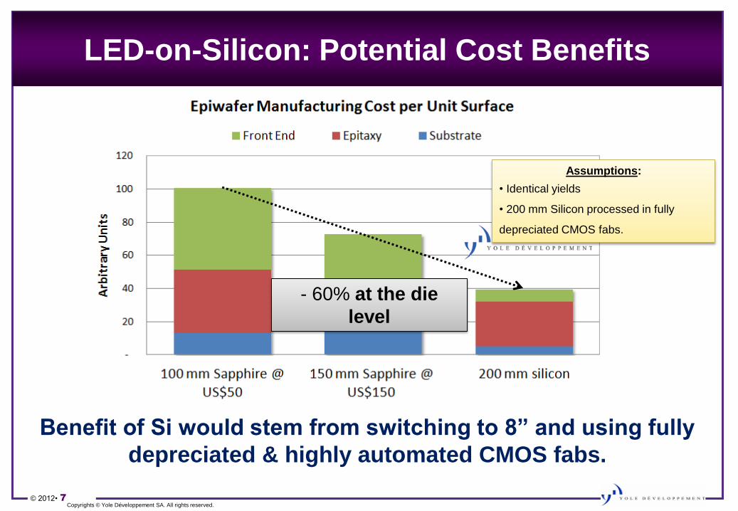
LED-on-Silicon: Potential Cost Benefits
Benefit of Si would stem from switching to 8” and using fully
depreciated & highly automated CMOS fabs.
Assumptions:
• Identical yields
• 200 mm Silicon processed in fully
depreciated CMOS fabs.
- 60% at the die
level

© 2012• 8
Copyrights © Yole Développement SA. All rights reserved.
Is Silicon Taking Over (yet)?
Silicon 2” 4” 6”
Sapphire, SiC ?

© 2012• 9
Copyrights © Yole Développement SA. All rights reserved.
Potential Benefits:
CMOS processing Wafer Price Higher Thermal
Conductivity
Non Transparent
Material
• Mature, efficient
(automated) & high
yield
• Large process
toolbox
Silicon is cheaper
than sapphire and
will likely remain so.
Better
Temperature
Homogeneity
More accurate
Surface
Temperature
Measurement
• Low cost: up to
10x improvement
vs. 2” sapphire (!?)
• New LED
structures ?
• Low wafer price
• 200 mm available
• But not semi
standard (yet?)
Improved
Binning Yield ?
Improved
Run/Run
repeatability ?
Direct manufacturing cost Potential yield benefits

© 2012• 10
Copyrights © Yole Développement SA. All rights reserved.
Main Challenges:
Lattice
Mismatch
Thermal Expansion
Coefficient
Mismatch
Melt Back
Blue Light
Absorption by
Wafer
Impact Epitaxial
Defect
• Wafer Bow • In-homogeneity
• Layer Cracking
Poor epitaxy Poor light
output
Sapphire
Bad Bad No No
Silicon
Worse Much worse Yes
Yes

© 2012• 11
Copyrights © Yole Développement SA. All rights reserved.
Main Challenge: TEC Mismatch
Before Epitaxy: During Epitaxy:
Hot
Cold Cold
Wafer
After epitaxy:
Stress!
Inhomogeneity
low binning yields
GaN layer
Cracking
Laytec Lattice Power
Solutions: Strain management layers, patterned
substrates, nanostructures…

© 2012• 12
Copyrights © Yole Développement SA. All rights reserved.
Main Challenges:
Lattice
Mismatch
Thermal Expansion
Coefficient
Mismatch
Melt Back
Blue Light
Absorption
by Wafer
Impact Epitaxial
Defect
• Wafer Bow • Inhomogeneity
• Layer Cracking
Poor epitaxy Poor light
output
Sapphire
Bad Bad No No
Silicon
Worse
Much worse Yes Yes

© 2012• 13
Copyrights © Yole Développement SA. All rights reserved.
Conditions for Success
#1: Must equal LED on Sapphire
performance.
© 2012• 14
Copyrights © Yole Développement SA. All rights reserved.
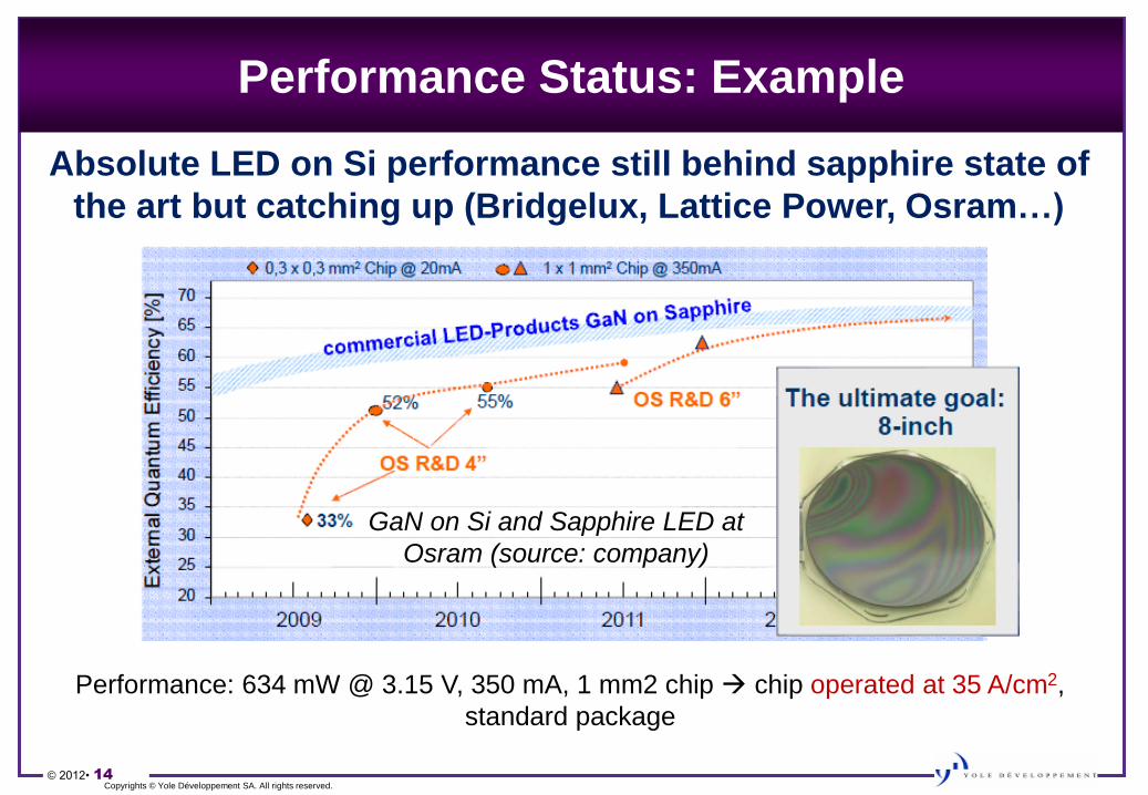
Performance Status: Example
Absolute LED on Si performance still behind sapphire state of
the art but catching up (Bridgelux, Lattice Power, Osram…)
GaN on Si and Sapphire LED at
Osram (source: company)
Performance: 634 mW @ 3.15 V, 350 mA, 1 mm2 chip chip operated at 35 A/cm2,
standard package

© 2012• 15
Copyrights © Yole Développement SA. All rights reserved.
Conditions for Success
#2: Must reach manufacturing
yields similar to
sapphire/SiC.

© 2012• 16
Copyrights © Yole Développement SA. All rights reserved.
Manufacturing & Binning Yields
Main Issue:
Wafer bow during epitaxy.
Getting worse with larger diameter!
Solutions include thicker wafers, curved pockets: requires
extremely stable and reproducible process
Wafer mapping of the Photoluminescence of Multi Quantum Wells with wafers seating in pockets with
different shapes. Source: Aixtron

© 2012• 17
Copyrights © Yole Développement SA. All rights reserved.
Are Yields Still important if Processing Since
CMOS Processing is Cheaper?
Yes: bad die carry the same cost as good ones!
Yields currently still lower than on 4” or 6” sapphire

© 2012• 18
Copyrights © Yole Développement SA. All rights reserved.
Conditions for Success
#3: Must be compatible with
CMOS, ideally on 200 mm
wafers (China: 150 mm fabs
also available)

© 2012• 19
Copyrights © Yole Développement SA. All rights reserved.
Compatibility with CMOS Fabs
Diameter Epiwafer Bow Wafer
Thickness Contamination
Wafer
Reflectivity
6” mininum
≥8” better < 50 – 60 um
725 um
(200 mm wafers) No gold
Reflective
surface
LED
on
Al2O3
Available but
(still)
expensive
Can be managed
but need very
thicker wafers
6”: 1 to 1.3 mm
Not compatible!
Used for bonding
and other layers
Incompatible
with equipment
sensors and
automations
LED
on Si
Available and
cheap.
150, 200,
300 mm
OK with strain
management
layers.
> 725 um: can
be thinned down
Used for bonding
and other layers
OK

© 2012• 20
Copyrights © Yole Développement SA. All rights reserved.
Conditions for Success: Summary
• Performance Must equal LED on Sapphire.
– Coming close.
• Must reach yields similar to Sapphire/SiC
– Still far away and needing significant improvement
• Must be CMOS compatible, 200 mm preferable
– Still some efforts needed
?
?
Incentive for LED-On-Si is COST not performance!

© 2012• 21
Copyrights © Yole Développement SA. All rights reserved.
Players and Recent News
• Most LED makers have LED on Si research programs:
– OSRAM
– Philips Lumileds
– Samsung
– Bridgelux + Toshiba
– Epistar
– Lattice Power
– TSMC…
• Multiple startups (e.g.: Aledia…)
• Bridgelux/Toshiba, Lattice Power, Plessey committed to Si transition.
Samsung also has strong incentive (CMOS fabs available)
• Most still undecided or in “defensive mode”
• New LED industry business models?
– Azzurro offering GaN on Si templates or full LED epiwafers fabless LED
makers.
Bridgelux 8” LED
Epiwafer
Osram 6” LED
Epiwafer Lattice Power
Led-On-Si chip

© 2012• 22
Copyrights © Yole Développement SA. All rights reserved.
Players and Recent News
Mixed signals at TSMC and Epistar:
TSMC: – “it is difficult for 8-inch Si-substrate GaN wafers to replace sapphire wafers to become
mainstream LED material because the former's manufacturing process is complicated and
brightness of LED chips is lower” – Jacob Tam, President TSMC Solid State Lighting, January
2013.
– “It is understood that in the current stage, TSMC Solid State Lighting GaN-on-Silicon and
sapphire substrate LED production line revenue is 50%, differentiated by using high-power and
low-power LEDs” – Digitime April 2013.
EPISTAR:
– Epistar transferred its GaN LED structure to an Si with Azzurro templates in just 16 weeks.
While Epistar has not announced plans for production of GaN-on-Si LEDs – PR Oct 2012
– Chairman Lee Biing-jye, indicated that yield rates for Si-substrate GaN wafers are still low and
Epistar is developing production technology for breakthrough”. - Digitime. Jan 2013
© 2012• 23
Copyrights © Yole Développement SA. All rights reserved.
Players and Recent News
But others moving on:
Bridgelux (US)/ Toshiba (JP):
• December 2012: Toshiba says it is shipping GaN-on-SI LEDs but no evidence yet of
products that use the LEDs have been verified on the market
• April 2013: Bridgelux sells silicon IP to Toshiba.
Plessey (UK)
• March 2013: Plessey announces shipment of GaN-on-Si LEDs using 6-in wafers but
first products only offer flux output in the 1-3-lm range 15-36 lm/W at 3.3V / 25 mA)
• Target for next product release: 60-70 lm/W
Lattice Power:
• Feb 2013: volume production of high power chips but still on 2” Si wafers. Not much
cost saving vs. sapphire but plan to switch to 6” soon.
• Currently run 15k to 20k wafers per month.

© 2012• 24
Copyrights © Yole Développement SA. All rights reserved.
Start-up or LED
company willing to
scale up capacity
without massive
CAPEX “Fabless”
model
Will LED-on-Si Happen?
• Still some technology hurdles: yields, full CMOS compatibility.
• LED on Si better suited for some type of LEDs than others and
breakeven point not the same for all manufacturers.
Large Semiconductor
company with existing
CMOS capacity
willing to enter the
LED Market
Tier one LED Maker
with advanced LED
on sapphire
technology and large
installed capacity
If technology hurdles are cleared, LED-On-Si will be adopted
by some LED manufacturers but not necessarily become
the standard.

© 2012• 25
Copyrights © Yole Développement SA. All rights reserved.
Will LED-on-Si Happen?
• It’s a cost game ($/lumen)!
• Si enables 200 mm in CMOS fabs
• Sapphire/SiC = moving targets!
Price
declining 8” possible (?)
Performance improving
(epitaxy, PSS…)
(Yole Developpement) Monocrystal DOE Roadmap
Maybe…

© 2012• 26
Copyrights © Yole Développement SA. All rights reserved.
Our Scenario
• If technology hurdles are cleared, LED-on-Si will be adopted by some LED maker, but
not necessarily become the industry standard.
Scenario #1:
Current LED-on-Si
proponent fails to move to
mass manufacturing.
Industry refocuses attention
on Sapphire, stimulating
adoption of 6” wafers and
possibly resuming R&D
effort on 8”
Scenario #2:
Current LED-on-Si
proponent successfully
moves to mass
manufacturing but fails to
generate massive cost
benefits and differentiations
LED-On Si adoption
remains limited to these few
companies. The bulk of the
industry continues
leveraging on its sapphire
(or SiC) platform
Scenario #3:
Current LED-on-Si
proponent are successful
and demonstrate
differentiating cost benefits
The rest of the industry tries
to emulate this success and
eventually massively
switches to LED-on-Si
complete disruption of the
sapphire wafer industry

© 2012• 27
Copyrights © Yole Développement SA. All rights reserved.
THANK YOU!
www.i-micronews.com
www.yole.fr
Contacts (US):
Michael McLaughlin: [email protected]
650-931-2552