lecture notesvemu.org/uploads/lecture_notes/30_12_2019_597530649.pdfthe 8086 microprocessor is...
TRANSCRIPT

Microprocessors & Microcontrollers N.KIRAN KUMAR
LECTURE NOTES
ON
MICROPROCESSORS & MICROCONTROLLERS(15A04607)
III B. Tech II Semester
Prepared byMr. N. KIRAN KUMAR, Asst. Professor
DEPT. OF ECE
1
Microprocessors & Microcontrollers N.KIRAN KUMAR
Syllabus
JAWAHARLAL NEHRU TECHNOLOGICAL UNIVERSITY ANANTAPURB. Tech III-II Sem. (ECE)
15A04607MICROPROCESSORS AND MICROCONTROLLERS
Course Outcomes:
After completion of this subject the students will be able to :
1. Do programming with 8086 microprocessors2. Understand concepts of Intel x86 series of processors3. Program MSP 430 for designing any basic Embedded System4. Design and implement some specific real time applications Using MSP 430 low power microcontroller.
UNIT IIntroduction-8086 Architecture-Block Diagram, Register Organization, Flag Register, Pin Diagram,Timing and Control Signals, System Timing Diagrams, Memory Segmentation, Interrupt structure of 8086and Interrupt Vector Table. Memory organization and memory banks accessing.
UNIT IIInstruction Formats -Addressing Modes-Instruction Set of 8086, Assembler Directives- Macros andProcedures.- Sorting, Multiplication, Division and multi byte arithmetic code conversion. StringManipulation instructions-Simple ALPs.
UNIT IIILow power RISC MSP430 – block diagram, features and architecture, variants of the MSP430 family viz.MSP430x2x, MSP430x4x, MSP430x5x and their targeted Applications, MSP430x5x series block diagram,Addressing modes, Instruction set Memory address space, on-chip peripherals (analog and digital), andRegister sets. Sample embedded system on MSP430 microcontroller.
UNIT-IVI/O ports pull up/down resistors concepts, Interrupts and interrupt programming, Watchdog timer, Systemclocks, Low Power aspects of MSP430: low power modes, Active vs Standby current consumption,FRAM vs Flash for low power & reliability. Timer & Real Time Clock (RTC), PWM control, timinggeneration and measurements. Analog interfacing and data acquisition: ADC and Comparator in MSP430,data transfer using DMA.
UNIT-V
2
Microprocessors & Microcontrollers N.KIRAN KUMAR
Serial communication basics, Synchronous/Asynchronous interfaces (like UART, USB, SPI, and I2C).UART protocol, I2C protocol, SPI protocol. Implementing and programming UART, I2C, SPI interfaceusing MSP430, Interfacing external devices. Implementing Embedded Wi-Fi using CC3100
UNIT-IIntroductionDefinition
The microprocessor is a multipurpose, programmable device(IC) that reads binary instructionsfrom the memory and process the data according to the instructions and then produces the output.
Features of Microprocessor
Some of the features of any microprocessor are-
Cost effective: The microprocessor chips are available at low prices and results its low cost.
Size: The microprocessor is of small size chip, hence it is portable.
Low power consumption: Microprocessors are manufactured by using metal oxide semiconductor technology, which haslow power consumption.
Versatility: The microprocessors are versatile as the same chips in number of applications can be used by configuring thesoftware program.
Reality: The failure rate of an IC in microprocessors is very low, hence it is reliable.
Microprocessors Characteristics These are the most important defining characteristics of a microprocessor −
Clock speed
Instruction set Word size
Clock SpeedEvery microprocessor has an internal clock that regulates the speed at which it executes
instructions and also synchronizes it with other components. The speed at which the microprocessorexecutes instructions is called clock speed. It determines the number of operations per second theprocessor can perform. Clock speeds are measured in MHz or GHz where 1 MHz means 1 million cyclesper second whereas 1 GHz equals to 1 billion cycles per second. Here cycle refers to single electric signalcycle.
Currently microprocessors have clock speed in the range of 3 GHz, which is maximum that currenttechnology can attain. Speeds more than this generate enough heat to damage the chip itself. To overcomethis, manufacturers are using multiple processors working in parallel on a chip.
Instruction Set
Each microprocessor is designed to execute a specific group of operations. This group of operationsis called an instruction set. This instruction set defines what the microprocessor can and cannot do. Theprograms can be written for microprocessor based on its instruction set.
3

Microprocessors & Microcontrollers N.KIRAN KUMAR
Word SizeNumber of bits that can be processed by a processor in a single instruction is called its word size.
Word size determines the amount of RAM that can be accessed at one go and total number of pins on themicroprocessor. Total number of input and output pins in turn determines the architecture of themicroprocessor. It depends upon the width of internal data bus, registers, ALU, etc.
An 8-bit microprocessor can process 8-bit data at a time. The word size or word length rangesfrom 4 bits to 64 bits depending upon the type of the microcomputer.
8086 Microprocessor Features:
The 8086 microprocessor is a 16 bit microprocessor. The term “16 bit” means that its arithmetic logic unit, internal registers and most of its instructions
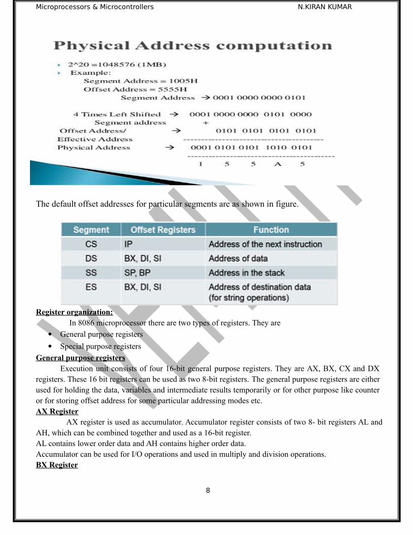
are designed to work with 16 bit binary words. The 8086 microprocessor has a 16 bit data bus. It can read data from or write data to memory or ports either 16 bits or 8 bits at a time. The 8086 microprocessor has a 20 bit address bus, so it can directly access 2^20 or 1,048,576 (1
MB) memory locations. The 8086 microprocessor can generate 16 bit I/O address; hence it can access 2^16 or 65536 ports. It performs the arithmetic and logical operations on bit, byte, word and decimal numbers including
multiplication and division. The 8086 microprocessor is designed to operate in two modes, the minimum mode and the
maximum mode. When only one CPU is used in the system, the 8086 microprocessor operates in the minimum
mode. In multiprocessor system, 8086 microprocessor operates in the maximum mode. The 8086 microprocessor supports multiprogramming ability.
Architecture of the 8086 microprocessorThe 8086 microprocessor is divided into two functional units, the Bus Interface Unit (BIU) and
the Execution Unit (EU). These two units can work simultaneously to increase system throughput. Thethroughput is a measure of number of instructions executed per unit time.Execution Unit (EU)
The EU contains ALU, Control Unit and registers. This feature enables the EU to executeinstructions and perform arithmetic and logical operations.
Functions of EU
fetch the instructions decode the instructions execute the instructions
Components of EU
General purpose registers Pointers and Index Registers Flag Registers
4

Microprocessors & Microcontrollers N.KIRAN KUMAR
Arithmetic Logic Unit (ALU) Instruction Decoder Control unit
General purpose registers:Execution unit consists of four 16-bit registers. They are AX, BX, CX and DX registers. These 16
bit registers can be used as two 8-bit registers. The general purpose registers are either used for holdingthe data, variables and intermediate results temporarily or for other purpose like counter or for storingoffset address for some particular addressing modes etc.
Pointer registers:There are three pointer registers. They are BP, SP and IP. These registers are 16 bit registers. The main
purpose of these registers is to store the offset address.Index registers:
There are two index registers available in 8086. They are SI and DI. These registers are 16 bitregisters. The main purpose of these registers is to store the source and destination addresses.
Arithmetic and logical unitArithmetic and logical unit performs all arithmetic and logical operations. The results of ALU
are stored in the accumulator.Instruction decoder
5

Microprocessors & Microcontrollers N.KIRAN KUMAR
The instructions from pre fetch instruction queue are taken and decoded in execution unit andthen the control signals are generated in the control circuit and then the instructions are executed.
Control unitExecution unit contains control circuit for controlling the internal operations. The control
signals are generated in the control unit.Bus Interface Unit (BIU)
The BIU sends out the address, fetches the instructions from the memory; read data from ports,and memory and writes data to the ports and memory. It provides a 16 bit bidirectional data bus and 20 bitaddress bus. The BIU is responsible for performing all external bus operations for execution unit.
Functions of BIU
Sends address to the Memory or I/O unit. Fetches instructions from Memory. Reads data from ports or Memory. Writes data on ports or Memory. Supports instruction queuing. Provides address relocation facility.
Components of BIU
Instruction Queue. Segment registers. Instruction Pointers. Address summer.
Instruction queueBIU contains an instruction queue. The size of instruction queue is 6 bytes and it follows FIFO
order. When the EU executes instructions, the BIU gets up to 6 bytes of the next instruction and storesthem in the instruction queue and this process is called instruction pre fetch. This is a process to speed upthe processor. These instructions are used in pipelining.
Pipelining is a process of fetching the next instruction while current instruction is executing.Segment Registers
In order to access the segments there are segment registers. The four segment register in 8086 are
Code segment register (CS)
Data segment register (DS)
Extra segment register (ES)
Stack segment register (SS)
Code segment register (CS): This is used for addressing memory location in the code segment of the memory, where the
executable program is stored. Code segment register contains the base address or starting address of codesegment.Data segment register (DS):
This register points to the data segment of the memory where the data is stored. Data segmentregister contains the base address or starting address of data segment.
6
Microprocessors & Microcontrollers N.KIRAN KUMAR
Extra Segment Register (ES): This register also refers to a segment in the memory which is another data segment in the
memory. Extra segment register contains the base address or starting address of extra segment.
Stack Segment Register (SS): This is used for addressing stack segment of the memory. The stack segment is that segment of
memory which is used to store stack data. Stack segment register contains the base address or startingaddress of stack segment.Instruction pointer (IP):
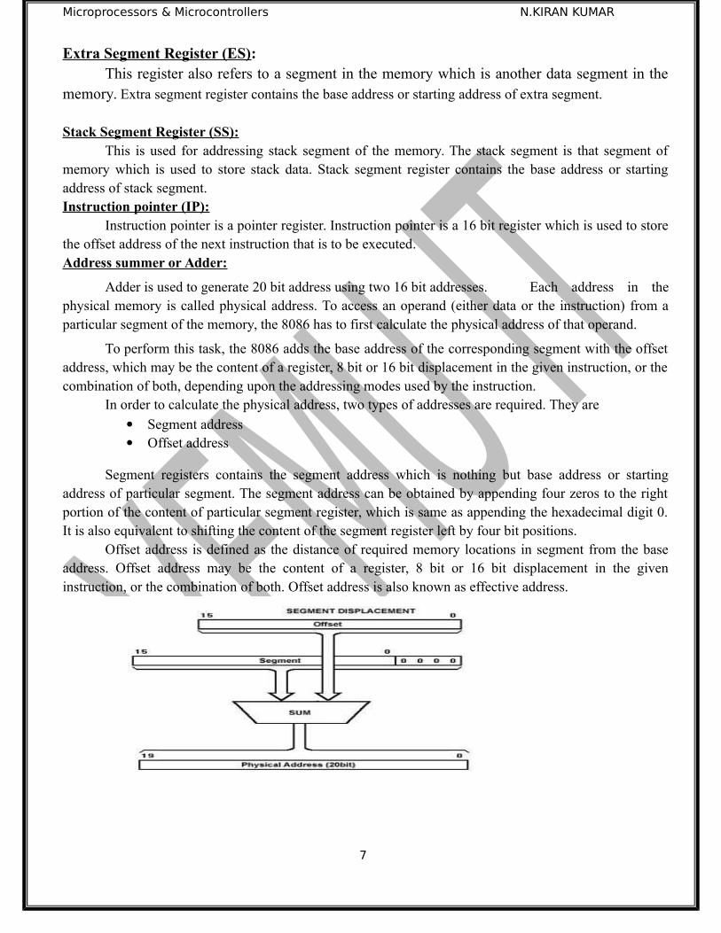
Instruction pointer is a pointer register. Instruction pointer is a 16 bit register which is used to storethe offset address of the next instruction that is to be executed.Address summer or Adder:
Adder is used to generate 20 bit address using two 16 bit addresses. Each address in thephysical memory is called physical address. To access an operand (either data or the instruction) from aparticular segment of the memory, the 8086 has to first calculate the physical address of that operand.
To perform this task, the 8086 adds the base address of the corresponding segment with the offsetaddress, which may be the content of a register, 8 bit or 16 bit displacement in the given instruction, or thecombination of both, depending upon the addressing modes used by the instruction.
In order to calculate the physical address, two types of addresses are required. They are
Segment address Offset address
Segment registers contains the segment address which is nothing but base address or startingaddress of particular segment. The segment address can be obtained by appending four zeros to the rightportion of the content of particular segment register, which is same as appending the hexadecimal digit 0.It is also equivalent to shifting the content of the segment register left by four bit positions.
Offset address is defined as the distance of required memory locations in segment from the baseaddress. Offset address may be the content of a register, 8 bit or 16 bit displacement in the giveninstruction, or the combination of both. Offset address is also known as effective address.
7
Microprocessors & Microcontrollers N.KIRAN KUMAR
The default offset addresses for particular segments are as shown in figure.
Register organization:In 8086 microprocessor there are two types of registers. They are
General purpose registers
Special purpose registers
General purpose registersExecution unit consists of four 16-bit general purpose registers. They are AX, BX, CX and DX
registers. These 16 bit registers can be used as two 8-bit registers. The general purpose registers are eitherused for holding the data, variables and intermediate results temporarily or for other purpose like counteror for storing offset address for some particular addressing modes etc.AX Register
AX register is used as accumulator. Accumulator register consists of two 8- bit registers AL andAH, which can be combined together and used as a 16-bit register. AL contains lower order data and AH contains higher order data.Accumulator can be used for I/O operations and used in multiply and division operations.BX Register
8

Microprocessors & Microcontrollers N.KIRAN KUMAR
BX register is known as Base register. Base register consists of two 8-bit registers BL and BH,which can be combined together and used as a 16-bit register. BX register is used to hold offset address forforming physical address in case of addressing modes. CX Register
CX register is known as Count Register. Count register consists of two 8-bit registers CL andCH, which can be combined together and used as a 16-bit register. CX register is used to hold the countvalue while executing the repeated string instructions and loop instructions. CL is used to hold the countvalue while executing the shift /rotate instructions. The count value indicates the number of times the samecode has to be executed when LOOP instruction is used, and the number of times the data has to be shiftedwhen rotate/ shift instruction is used.DX Register
DX register is known as Data Register. Data register consists of two 8-bit registers DL andDH, which can be combined together and used as a 16-bit register. Data register can be used as a portnumber in I/O operations when executing IN/OUT instructions. Data register is used to hold a part ofresult during multiplication operation and a part of dividend before a division operation.Special purpose registers:
There are three types of special purpose registers. They are pointer registers, index registers andflag registers. Pointer Registers The 16 bit pointers registers in 8086 microprocessor are IP, BP, and SP. Among pointer registersSP and BP registers are located in EU and IP register is located in BIU. The main purpose of pointerregisters is to hold the offset address. The pointer registers can also be used as general purpose registers. BP Register
BP register is known as base pointer. Base pointer is a 16 bit register and used to hold the offsetaddress of the data to be read from or written into the stack segment.SP Register
SP Register is known as stack pointer. SP Register is a 16 bit register and used to hold the offsetaddress of the data stored in the top of the stack. Sp is used along with SS register to decide the address atwhich the data is to be pushed or popped during the execution of PUSH/ POP instructions.IP Register
IP Register is known as instruction pointer. It is 16 bit register which is used to store the offsetaddress of the next instruction that is to be executed.Index Registers
Index registers are 16 bit registers which are used to store the offset address. Index registers areSI and DI registers. These registers are also used as general purpose registers.SI Register
SI Register is known as source index register or source register which contains the source addressof the data segment. It is a 16 bit register. SI register is used in string manipulations.DI Register
DI Register is known as destination index register or destination register which contains thedestination address of the data segment / extra segment. It is a 16 bit register. DI register is used in stringmanipulations.Flag Register
9

Microprocessors & Microcontrollers N.KIRAN KUMAR
Flag register indicates the status of the ALU results. A 16 flag register is used in 8086. It is divided intotwo parts
(a) Conditional code or status flags(b) Machine control flags
Condition code flagThe condition code flag is the lower byte of the 16-bit flag register. It contains 6 flags namely carry
flag (CF), parity flag (PF), auxiliary carry flag (AF), zero flag (ZF), sign flag (SF) and overflow flag (OF).Control flag
The control flag is the higher byte of the flag register. It contains three flags namely direction flag(D), interrupt flag (I) and trap flag (T).The complete bit configuration of 8086 is shown in the figure.
Carry Flag: Carry flag is set (CF=1), when there is a carry of MSB is generated in case of addition orborrow in case of subtraction. Otherwise it is said to be reset (CF=0).
Parity Flag: Parity flag is set (PF=1), if the lower byte of the result contains even number of 1’s. If there isodd number of 1’s in the result it is said to be reset (PF=0).
Sign Flag: Sign flag is set (SF=1), when the result of any computation is negative, otherwise it is said to bereset (SF=0).
Zero Flag: Zero flag is set (ZF=1), if the result of computation is zero. Otherwise it is said to be reset(ZF=0).
Auxiliary Carry Flag: Auxiliary flag is set (AF=1), if there is a carry is generated in the lowest nibble, i.e,bit three during addition, or borrow is generated in the lowest nibble, i.e, bit three, during subtraction.Otherwise it is said to be reset (AF=0).Over flow Flag: Overflow flag is set (OF=1), if an overflow occurs, i.e, if the result of a signed operation islarge enough to accommodate in a destination register. The result is of more than 7-bits in size in case of 8-bit signed operation and more than 15-bits in size in case of 16-bit sign operations, and then the overflowwill be set. Otherwise it is said to be reset (OF=0).Trap Flag: Trap flag is set (TF=1), when the processor enters the single step execution mode. Otherwise itis said to be reset (TF=0).
10

Microprocessors & Microcontrollers N.KIRAN KUMAR
Interrupt Flag: Interrupt flag is set (IF=1), when the interrupt requests are recognized by themicroprocessor, otherwise they are said to be reset (IF=0).Direction Flag: Direction flag is used by string instructions. This flag is said to be set (DF=1), when thestring is processed from the highest address towards the lowest address, i.e., auto decrementing mode.Direction flag is reset (DF=0), when the string is processed from the lowest address to the highest address,i.e., auto incrementing mode.
8086 Pin diagram
POWER SUPPLY :
8086 uses 5V DC power supply at VCC pin 40, and uses ground at VSS pin 1 and 20 for its properoperation.
CLOCK SIGNAL:
Clock signal is provided through Pin-19. It provides timing to the processor for operations. Itsfrequency is different for different versions, i.e. 5MHz, 8MHz and 10MHz.
ADDRESS/DATA BUS ( AD0-AD15 ):
These are 16 address/data bus which are multiplexed. AD0-AD7 carries low order byte data andAD8-AD15 carries higher order byte data. During the first clock cycle, it carries 16-bit address and afterthat it carries 16-bit data.
ADDRESS/STATUS BUS (A16-A19/S3-S6):
These are 4 address/status buses which are multiplexed. During the first clock cycle, it carries 4-bit address and later it carries status signals. The status of the interrupt enable flag bit (displayed on S5) is
11

Microprocessors & Microcontrollers N.KIRAN KUMAR
updated at the beginning of each clock cycle. The status line S6 is always low. The S4 and S3 combinedlyindicate which segment register is presently being used for memory access.
S4 S3 Function0 0 Extra segment0 1 Stack segment1 0 Code segment1 1 Data segment
S7/ :
BHE stands for Bus High Enable. It is available at pin 34 and used to indicate the transfer of datausing higher order data bus D8-D15. It also indicates whether whole word or byte is transferred. During
the first clock cycle is a low and remaining cycle status signal S7 is available.
BHE bar S7 Function 0 0 Whole word0 1 Upper byte from or to odd address1 0 Upper byte from or to even address1 1 None
RD:
It is available at pin 32 and is used to read the data for Read operation. It performs read operationeither from memory or IO device.
READY:
It is available at pin 32. It is an acknowledgement signal from slow I/O devices that data transfer iscompleted. It is an active high signal. When it is high, it indicates that the device is ready to transfer data.When it is low, it indicates wait state.
RESET:
It is available at pin 21 and is used to restart the execution. It causes the processor to immediatelyterminate its present activity. This signal is active high for the first 4 clock cycles to RESET themicroprocessor.
INTR:
It is available at pin 18. It is an interrupt request signal, which is sampled during the last clockcycle of each instruction to determine the availability interrupt. If interrupt request is pending theprocessor enters into interrupt acknowledge cycle. This can be done by enabling the interrupt flag. INTRis a level triggered interrupt.
NMI:
It stands for non-maskable interrupt and is available at pin 17. It is an edge triggered input, whichcauses an interrupt request to the microprocessor. A transition from low to high initiates the interruptresponse at the end of the instruction.
12

Microprocessors & Microcontrollers N.KIRAN KUMAR
RESET: This input causes the processor to terminate the current activity and start
execution from FFFF0 H. The signal is active high and must be active for at least fourclock cycles. It restarts execution when the RESET returns low. RESET is also internally synchronized.
TEST bar:
This input is examined by a 'WAIT' instruction. If the TEST input goes low, execution willcontinue, else, the processor remains in an idle state.
MN/ MX bar:
It stands for Minimum/Maximum mode and is available at pin 33. It indicates which type of modethe processor is to operate. When it is high, it operates in the minimum mode and when it is low itoperates in maximum mode.
INTA bar:
It is an interrupt acknowledgement signal and is available at pin 24. When the microprocessorreceives this signal, it has to accept the interrupt.
ALE:
It stands for address enable latch and is available at pin 25. A positive pulse is generated each timethe processor begins any operation. This signal indicates the availability of a valid address on the addressbus.
DEN bar:
It stands for Data Enable and is available at pin 26. It is used to enable Transreceiver and indicatesthat data is available on the data bus. The transceiver is a device used to separate data from themultiplexed address/data bus.
DT/R bar:
It stands for Data Transmit/Receive signal and is available at pin 27. It decides the direction of dataflow through the transreceiver. When it is high, data is transmitted out and when it is low data is received.
M/ :
This signal is used to distinguish between memory and I/O operations. When it is high, it indicatesI/O operation and when it is low indicates the memory operation. It is available at pin 28.
WR bar:
It stands for write signal and is available at pin 29. It is used to write the data into the memory orthe output device depending on the status of M/IO signal.
HOLD:
This signal indicates to the processor that external devices are requesting to access the address/databuses. It is available at pin 31.HOLD signal is used in DMA (Direct Memory Access) operation.
HLDA:13

Microprocessors & Microcontrollers N.KIRAN KUMAR
It stands for Hold Acknowledgement signal and is available at pin 30. This signal acknowledgesthe HOLD signal. This acknowledgement signal is sent by the processor to other devices when it receivesHOLD request signal. HLDA signal is used in DMA (Direct Memory Access) operation.
QS1 and QS0:
These are queue status signals and are available at pin 24 and 25. These signals provide thestatus of instruction queue. Their conditions are shown in the following table
QS0 QS1 Status
0 0 No operation
0 1 First byte of op code from the queue
1 0 Empty the queue
1 1 Subsequent byte from the queue
S0, S1, S2:
These are the status signals that provide the status of operation, which is used by the BusController 8288 to generate memory & I/O control signals. These are available at pin 26, 27, and 28.Following is the table showing their status –
S2 S1 S0 Status
0 0 0 Interrupt acknowledgement
0 0 1 I/O Read
0 1 0 I/O Write
0 1 1 Halt
1 0 0 Op code fetch
1 0 1 Memory read
14

Microprocessors & Microcontrollers N.KIRAN KUMAR
1 1 0 Memory write
1 1 1 Passive
LOCK:
When this signal is active, it indicates to the other processers to prevent the access of system bus. Itis activated using the LOCK prefix on any instruction and remains active until completion of the nextinstruction.
RQ/GT1 and RQ/GT0:
These are the Request/Grant signals used by the other processors requesting the CPU to release thesystem bus in case of DMA (Direct Memory Access) operations. When the RQ0/RQ1 request signal isreceived by processor, then processor sends acknowledgment signal through GT0/GT1. RQ/GT0 has ahigher priority than RQ/GT1.
Timing and control signals:
Timing and control signals are minimum mode pin signals and maximum mode pin signals.
Minimum mode pin signals
HOLD
HLDA
WR BAR
M/
DT/R BAR
DEN BAR
INTA BAR
Maximum mode pin signals
RQ/GTO BAR
RQ/GT1 BAR
LOCK
S2 BAR
S1 BAR
S0 BAR
15

Microprocessors & Microcontrollers N.KIRAN KUMAR
QS1
QS0
System timing diagrams:
The timing diagram provides information about the various conditions of signals such as high/low,when a machine cycle is being executed. Without the knowledge of timing diagram it is not possible tomatch the peripheral devices to the microprocessors. These peripheral devices includes memories, portsetc. Such devices can only be matched with microprocessors with the help of timing diagram.Machine cycle : A basic microprocessor operation such as reading a byte from memory or writing a byteto a port is called a machine cycle (Bus cycle). A machine cycle consists of at least 4 clock cycles/ clockstates (T-states) for accessing the data.Instruction cycle: The time a microprocessor requires to fetch and execute an entire instruction isreferred to as an instruction cycle. An instruction cycle consists of one or more machine cycles.T-state: T-state is nothing but one subdivision of the operation performed in one clock period. Thesesubdivisions are internal state of the microprocessor synchronized with system clock.
So, an instruction cycle is made up of machine cycles, and a machine cycle is made up of states.The time for the state is determined by the frequency of the clock signal.
The 8086 has a combined address and data bus commonly referred as a time multiplexed addressand data bus. The main reason behind multiplexing address and data over the same pins is the maximumutilization of processor pins and it facilitates the use of 40 pin standard DIP package. The bus can be demultiplexed using a few latches and transreceivers, when ever required. Basically, all the processor buscycles consist of at least four clock cycles. These are referred to as T1, T2, T3, and T4. The address istransmitted by the processor during T1. It is present on the bus only for one cycle.
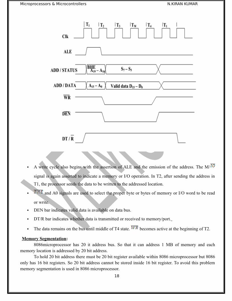
Read cycle
16

Microprocessors & Microcontrollers N.KIRAN KUMAR
• The read cycle begins in T1 with the assertion of address latch enable (ALE) signal and also M /
signal. During the negative going edge of this signal, the valid address is latched on the local
bus. From T1 to T4, the M/ signal indicate a memory or I/O operation is to be performed..
• and A0 signals are used to select the proper byte or bytes of memory or I/O word to be read
or write.
• At T2, the address is removed from the local bus and is sent to the output. The read ( ) control
signal is also activated in T2.
• The read ( ) signal causes the address device to enable its data bus drivers. After goes low,
the valid data is available on the data bus.
• The addressed device will drive the READY line high. When the processor returns the read signalto high level.
• DEN bar indicates valid data is available on data bus.
• DT/R bar indicates whether data is transmitted or received to memory/port.
Write cycle
17
Microprocessors & Microcontrollers N.KIRAN KUMAR
• A write cycle also begins with the assertion of ALE and the emission of the address. The M/
signal is again asserted to indicate a memory or I/O operation. In T2, after sending the address in
T1, the processor sends the data to be written to the addressed location.
• and A0 signals are used to select the proper byte or bytes of memory or I/O word to be read
or write.
• DEN bar indicates valid data is available on data bus.
• DT/R bar indicates whether data is transmitted or received to memory/port.
• The data remains on the bus until middle of T4 state. becomes active at the beginning of T2.
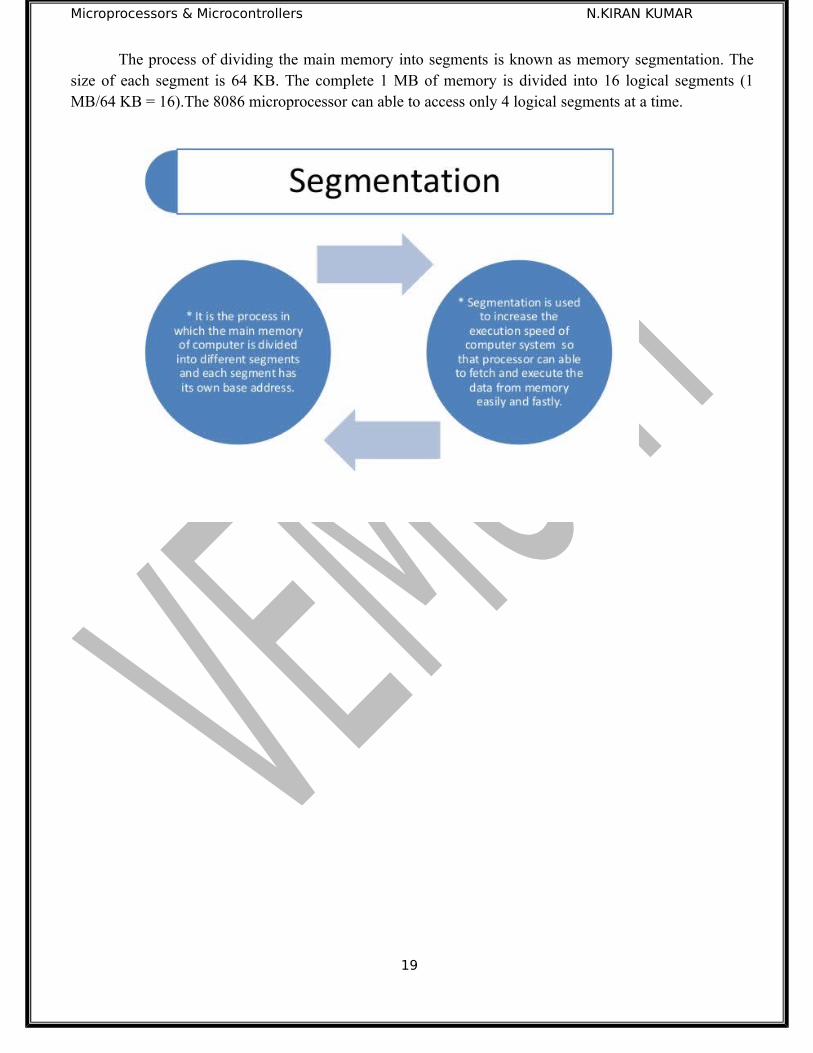
Memory Segmentation:8086microprocessor has 20 it address bus. So that it can address 1 MB of memory and each
memory location is addressed by 20 bit address.To hold 20 bit address there must be 20 bit register available within 8086 microprocessor but 8086
only has 16 bit registers. So 20 bit address cannot be stored inside 16 bit register. To avoid this problemmemory segmentation is used in 8086 microprocessor.
18
Microprocessors & Microcontrollers N.KIRAN KUMAR
The process of dividing the main memory into segments is known as memory segmentation. Thesize of each segment is 64 KB. The complete 1 MB of memory is divided into 16 logical segments (1MB/64 KB = 16).The 8086 microprocessor can able to access only 4 logical segments at a time.
19

Microprocessors & Microcontrollers N.KIRAN KUMAR
Interrupt structure of 808620

Microprocessors & Microcontrollers N.KIRAN KUMAR
INTERRUPTIn general, the process of interrupting the normal program execution to carry out a specific
task/work is referred to as interrupt. The interrupt is initiated by a signal generated by an external device or
by a signal generated internal to the processor.OCCURRENCE OF INTERRUPTThe processor can be interrupted in the following ways
i) by an external signal generated by a peripheral,ii) by an internal signal generated by a special instruction in the program,iii) by an internal signal generated due to occurrence of some condition.
EXTERNAL SIGNAL An 8086 can get interrupt from an external signal applied to the Non Mask able Interrupt (NMI)
input pin, or the interrupt (INTR) input pin.SPECIAL INSTRUCTION
8086 supports a special instruction, INT to execute special program. At the end of interrupt service
routine, execution is usually returned to the interrupted program.
CONDITION PRODUCED BY THE INSTRUCTIONAn 8086 is interrupted by the some condition produced in the 8086 by the execution of an
instruction.For example divide by zero: program execution will automatically be interrupted if you attempt to
divide an operand by zero.At the end of each instruction cycle 8086 checks to see if there is any interrupt request. If
so, 8086 responds to interrupt by performing series of actions.Interrupt process
When a microprocessor receives an interrupt signal it stops executing current normal program,
save the status (or content) of various registers (IP, CS and flag registers in case of 8086) in stack and then
the processor executes a subroutine/procedure in order to perform the specific task/work requested by the
interrupt. The subroutine/procedure that is executed in response to an interrupt is also called Interrupt
Service Subroutine. (ISR). At the end of ISR, the stored status of registers in stack is restored to respective
registers, and the processor resumes the normal program execution from the point {instruction) where it
was interrupted.
21

Microprocessors & Microcontrollers N.KIRAN KUMAR
INTERRUPT
CYCLE OF
8086
1. It
decrements stack pointer by 2 and pushes the flag register on the stack.2. It disables the INTR interrupt input by clearing the interrupt flag (IF) in flag register.3. It resets the trap flag in the flag register.4. It decrements the stack pointer by 2 and pushes the current code segments register contents
on the stack.5. It decrements the stack pointer by 2 and pushes the current instruction pointer contents on
the stack.6. It does an indirect far jump at the start of the procedure by loading the CS and IP values for
the start of the interrupt service routine (ISR).
An IRET instruction at the end of the interrupt service procedure returns execution to the main program.CLASSIFICATION OF INTERRUPTS
In general the interrupts can be classified in the following three ways:1. Hardware and software interrupts2. Vectored and Non Vectored interrupt:3. Mask able and Non Mask able interrupts.HARDWARE INTERRUPTS
The interrupts initiated by external hardware by sending an appropriate signal to the Interrupt pin
of the processor is called hardware interrupt. The 8086 processor has two Interrupt pins INTR and NMI. The interrupts initiated by applying
appropriate signal to these pins are called hardware interrupts of 8086.SOFTWARE INTERRUPTS
22

Microprocessors & Microcontrollers N.KIRAN KUMAR
The software interrupts are program instructions. These instructions are inserted at desired
locations in a program. While running a program, if software interrupt instruction is encountered then the
processor initiates an interrupt. The 8086 processor has 256 types of software interrupts. The software interrupt instruction is INT
n, where n is the type number in the range 0 to 255.VECTORED INTERRUPTS
When an interrupt signal is accepted by the processor, if the program control automatically
branches to a specific address (called vector address) then the interrupt is called vectored interrupt. The
automatic branching to vector address is predefined by the manufacturer of processors. (In these vector
addresses the interrupt service subroutines (ISR) are stored). NON-VECTORED INTERRUPTS
In non-vectored interrupts the interrupting device should supply the address of the ISR to be
executed in response to the interrupt. In 8086 there are 17 vectored interrupts. The vector address for an
8086 interrupt is obtained from a vector table implemented in the first 1kb memory space (00000h to
03FFFh). MASKABLE AND NON MASKABLE INTERRUPTS
The processor has the facility for accepting or rejecting hardware interrupts. Programming the
processor to reject an interrupt is referred to as masking or disabling and programming the processor to
accept an interrupt is referred to as unmasking or enabling. In 8086 the interrupt flag (IF) can be set to unmask or enable all hardware interrupts and IF is
cleared to zero to mask or disable a hardware interrupts except NMI.The interrupts whose request can be either accepted or rejected by the processor are called
maskable interrupts. The interrupts whose request has to be definitely accepted (or cannot be rejected) by the processor
are called non-maskable interrupts. Whenever a request is made by non-maskable interrupt, the processor
has to definitely accept that request and service that interrupt by suspending its current program and
executing an ISR. In 8086 processor all the hardware interrupts initiated through INTR pin are maskable by clearing
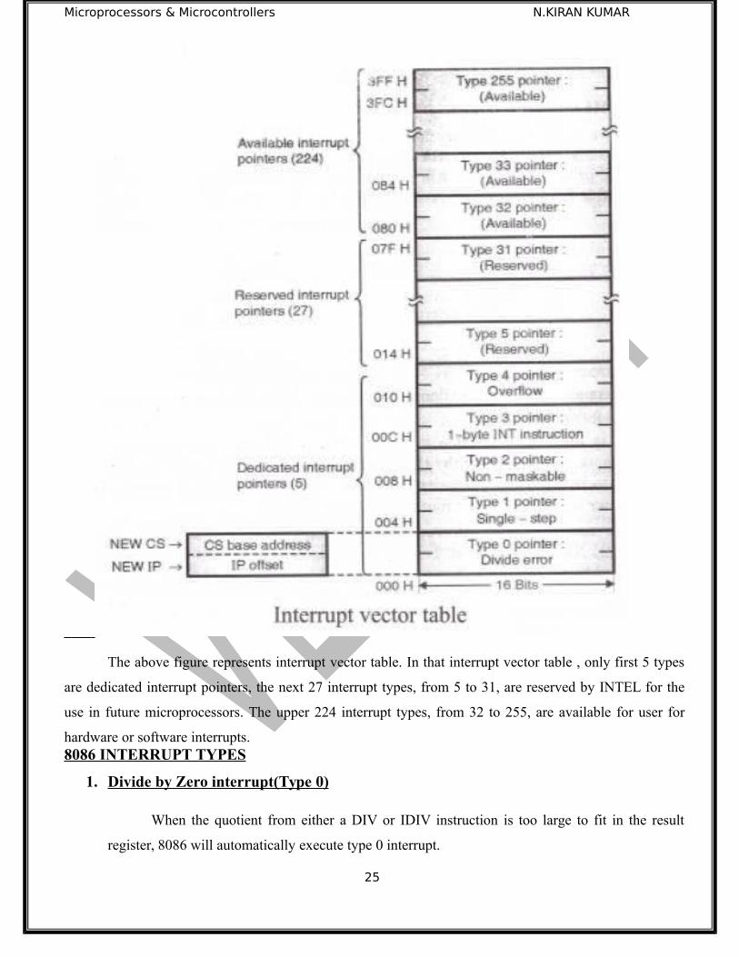
interrupt flag (IF). The interrupt initiated through NMI pin and all software interrupts are non-maskable. INTERRUPT VECTOR TABLE
The first 1Kbyte of memory of 8086 (00000 to003FF) is set aside as a table for storing the starting
addresses of Interrupt Service Routines (ISR). The starting address of an ISR is often called the Interrupt
Vector or Interrupt Pointer. The block of memory is referred as Interrupt Vector Table.
When 8086 responds to an interrupt, it gets the new values of CS and IP registers from four
memory addresses. Since 4 bytes are required to store the CS and IP values for each interrupt service
routines.
23

Microprocessors & Microcontrollers N.KIRAN KUMAR
The figure shows how 256 interrupts are arranged in the memory table. Each interrupt type is given
a number from 0 to 255 and the address of each interrupt is found by multiplying the type by 4. Example: For type 11, the interrupt address is 11*4=44=0002C H
For type 2, the interrupt address is 2*4=8=00008HThese 256 interrupts are groups as three types of interrupts, namely
Dedicated interrupts Reserved interrupts Available interrupts
Dedicated interrupts:There are 5 dedicated interrupts in 8086 microprocessor. The interrupts from type 0 to type 4 are
known as dedicated interrupts. These interrupts are dedicated to particular application so it is named asdedicated interrupts.
Reserved interrupts:There are 27 reserved interrupts in 8086 microprocessor. The interrupts from type 5 to type 31 are
known as reserved interrupts. These interrupts are reserved for future purpose, so it is named as reservedinterrupts.
Available interrupts:There are 224 reserved interrupts in 8086 microprocessor. The interrupts from type 32 to type 255
are known as reserved interrupts. These interrupts are available for users, so it is named as availableinterrupts.
24
Microprocessors & Microcontrollers N.KIRAN KUMAR
The above figure represents interrupt vector table. In that interrupt vector table , only first 5 types
are dedicated interrupt pointers, the next 27 interrupt types, from 5 to 31, are reserved by INTEL for the
use in future microprocessors. The upper 224 interrupt types, from 32 to 255, are available for user for
hardware or software interrupts.8086 INTERRUPT TYPES
1. Divide by Zero interrupt(Type 0)
When the quotient from either a DIV or IDIV instruction is too large to fit in the result
register, 8086 will automatically execute type 0 interrupt.
25
Microprocessors & Microcontrollers N.KIRAN KUMAR
2. Single Step Interrupt(Type 1)
The type 1 interrupt is then single step trap. In the single step mode, the system will execute
one instruction and wait for further direction from user. Then user can examine the contents of
registers and memory locations and if they are correct, user can tell the system to execute the next
instruction. This feature is useful for debugging assembly language program.
An 8086 system is used in single step mode by setting the trap flag. If trap flag is set, the
8086 will automatically execute a type 1 interrupt after execution of each instruction.
3. Non Maskable Interrupt (Type 2)
As the name suggests, this interrupt cannot be disabled by any software instruction. This
interrupt is activated by low to high transition on NMI input pin. In response 8086 will do a type 2
interrupt.
The characteristics of NMI are as follows:
These interrupts are known as non-maskable types.
These interrupts have highest priority than INTR interrupt.
These interrupts are edge triggered which are low to high transition.
In order to function they must remain high for at least 2 cycles of CLK.
These interrupts do not send out any form of acknowledgements.4. Breakpoint Interrupt (Type 3)
The type 3 interrupt is used to implement breakpoint function in the system. This type of
interrupt indicates termination of the program. The type 3 interrupt is produced by execution of
INT 3 instruction.
5. Overflow Interrupt (Type 4)
The type 4 interrupt is used to check overflow condition after any signed arithmetic
operation in the system. The 8086 overflow flag, OF, will be represented in the destination register
or memory location.
Memory organization & memory banks accessing8086 is a 16 bit microprocessor and hence can access two bytes of data in one memory. But
commercially available memory chips are only one byte size, ie. They can store only one byte in amemory location. Obviously, to store 16 bit data, two successive memory locations are used and lowerbyte of 16 bit data can be stored in first memory location while the second byte is stored in next memorylocation.
26
Microprocessors & Microcontrollers N.KIRAN KUMAR
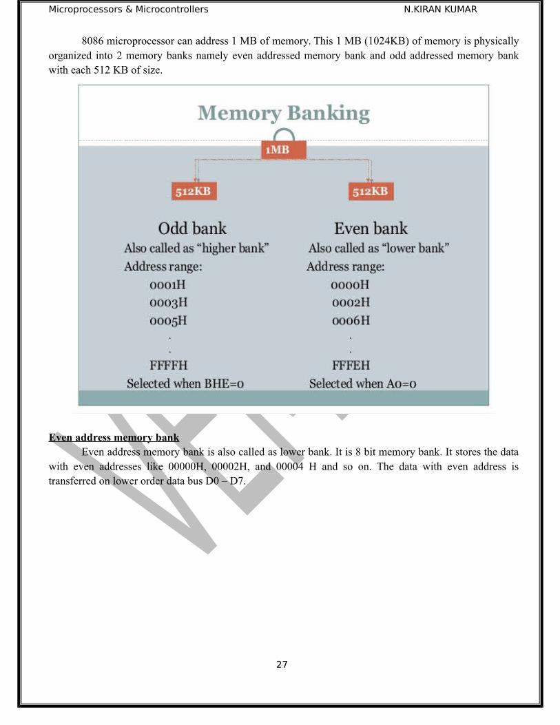
8086 microprocessor can address 1 MB of memory. This 1 MB (1024KB) of memory is physicallyorganized into 2 memory banks namely even addressed memory bank and odd addressed memory bankwith each 512 KB of size.
Even address memory bankEven address memory bank is also called as lower bank. It is 8 bit memory bank. It stores the data
with even addresses like 00000H, 00002H, and 00004 H and so on. The data with even address istransferred on lower order data bus D0 – D7.
27
Microprocessors & Microcontrollers N.KIRAN KUMAR
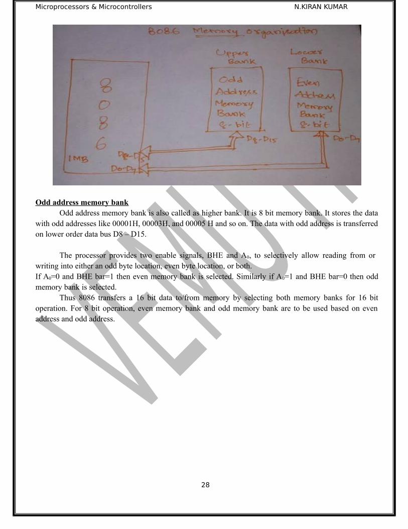
Odd address memory bankOdd address memory bank is also called as higher bank. It is 8 bit memory bank. It stores the data
with odd addresses like 00001H, 00003H, and 00005 H and so on. The data with odd address is transferredon lower order data bus D8 – D15.
The processor provides two enable signals, BHE and A0, to selectively allow reading from orwriting into either an odd byte location, even byte location, or both. If A0=0 and BHE bar=1 then even memory bank is selected. Similarly if A0=1 and BHE bar=0 then oddmemory bank is selected.
Thus 8086 transfers a 16 bit data to/from memory by selecting both memory banks for 16 bitoperation. For 8 bit operation, even memory bank and odd memory bank are to be used based on evenaddress and odd address.
28

Microprocessors & Microcontrollers N.KIRAN KUMAR
UNIT-II8086 Addressing modes
The addressing mode indicates the way of locating the data or operands in the memory. It alsospecifies the way in which the data or operand is accessed from the memory.Types of addressing modes
Immediate addressing mode Register addressing mode Data memory addressing mode Program memory addressing mode Stack memory addressing mode
Immediate addressing modeIn immediate addressing mode, the data is specified in the instruction. The data can be 8 bit or 16
bit data.Example:
MOV AL, 50H; move the data 50H to AL MOV BX, 230A H; move the data 230aH to BX
Register addressing modeIn register addressing mode, the data is present in the register and this data is moved and the result
is stored in the register.
Example: MOV AL, BL; Move the content of BL to AL MOV CX, BX; Move the content of BX to CX ADD CL,BL; Add the contents of CL and BL and store the result in CL ADD BX, DX; Add the contents of BX and DX and the results is stored in DX
Data memory addressing modes:In data memory addressing mode the data can be accessed through offset address. The term effective
address (EA) represents the offset address of the data within a segment, which is obtained by differentmethods, depending upon the addressing mode that is used in the instruction.Let us consider the various register values for discussion of data memory addressing modes-
29
Microprocessors & Microcontrollers N.KIRAN KUMAR
REGISTER CS DS SS ES BX BP SI DIVALUE 1000H 3000H 4000H 6000H 2000H 1500H 2500H 3500H
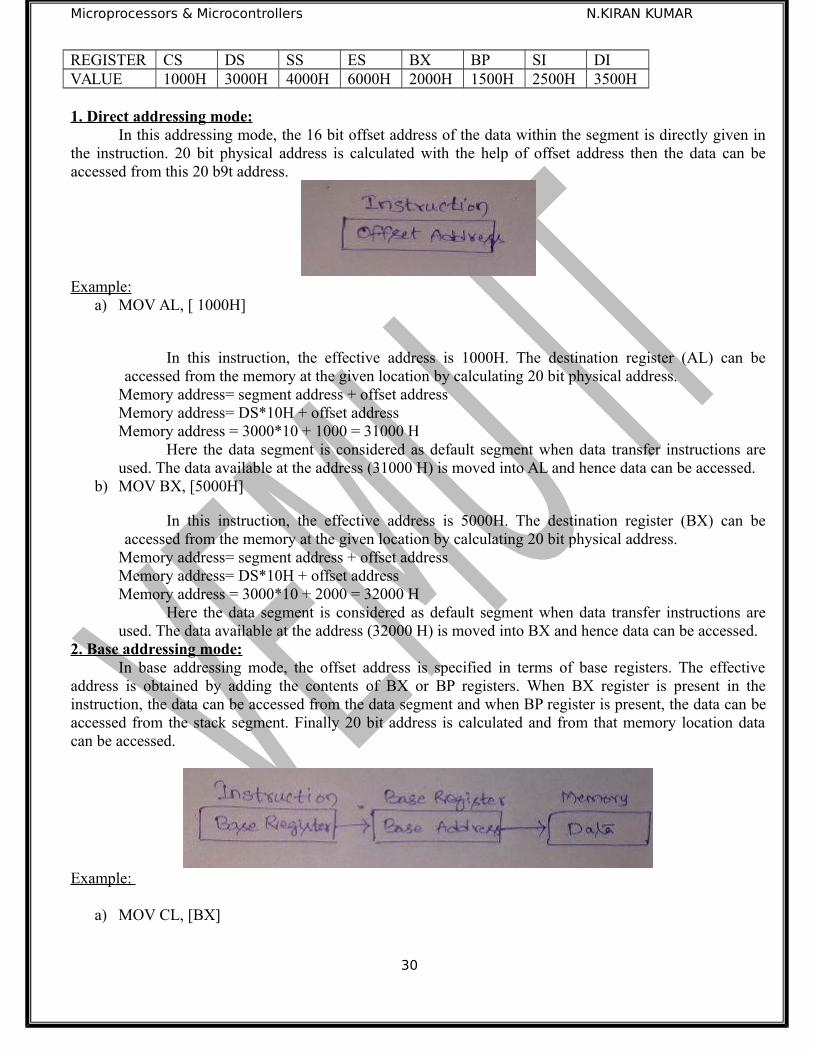
1. Direct addressing mode:In this addressing mode, the 16 bit offset address of the data within the segment is directly given in
the instruction. 20 bit physical address is calculated with the help of offset address then the data can beaccessed from this 20 b9t address.
Example:a) MOV AL, [ 1000H]
In this instruction, the effective address is 1000H. The destination register (AL) can beaccessed from the memory at the given location by calculating 20 bit physical address.
Memory address= segment address + offset addressMemory address= DS*10H + offset addressMemory address = 3000*10 + 1000 = 31000 H
Here the data segment is considered as default segment when data transfer instructions areused. The data available at the address (31000 H) is moved into AL and hence data can be accessed.
b) MOV BX, [5000H]
In this instruction, the effective address is 5000H. The destination register (BX) can beaccessed from the memory at the given location by calculating 20 bit physical address.
Memory address= segment address + offset addressMemory address= DS*10H + offset addressMemory address = 3000*10 + 2000 = 32000 H
Here the data segment is considered as default segment when data transfer instructions areused. The data available at the address (32000 H) is moved into BX and hence data can be accessed.
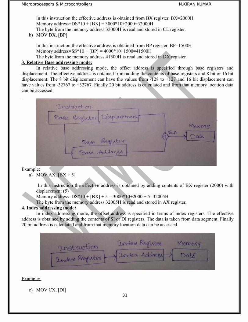
2. Base addressing mode:In base addressing mode, the offset address is specified in terms of base registers. The effective
address is obtained by adding the contents of BX or BP registers. When BX register is present in theinstruction, the data can be accessed from the data segment and when BP register is present, the data can beaccessed from the stack segment. Finally 20 bit address is calculated and from that memory location datacan be accessed.
Example:
a) MOV CL, [BX]
30
Microprocessors & Microcontrollers N.KIRAN KUMAR
In this instruction the effective address is obtained from BX register. BX=2000HMemory address=DS*10 + [BX] = 3000*10+2000=32000HThe byte from the memory address 32000H is read and stored in CL register.
b) MOV DX, [BP]
In this instruction the effective address is obtained from BP register. BP=1500HMemory address=SS*10 + [BP] = 4000*10+1500=41500HThe byte from the memory address 41500H is read and stored in DX register.
3. Relative Base addressing mode:In relative base addressing mode, the offset address is specified through base registers and
displacement. The effective address is obtained from adding the contents of base registers and 8 bit or 16 bitdisplacement. The 8 bit displacement can have the values from -128 to +127 and 16 bit displacement canhave values from -32767 to +32767. Finally 20 bit address is calculated and from that memory location datacan be accessed.
Example:a) MOV AX, [BX + 5]
In this instruction the effective address is obtained by adding contents of BX register (2000) withdisplacement (5)Memory address=DS*10 + [BX] + 5 = 3000*10+2000 + 5=32005HThe byte from the memory address 32005H is read and stored in AX register.
4. Index addressing mode:In index addressing mode, the offset address is specified in terms of index registers. The effective
address is obtained by adding the contents of SI or DI registers. The data is taken from data segment. Finally20 bit address is calculated and from that memory location data can be accessed.
Example:
c) MOV CX, [DI]31
Microprocessors & Microcontrollers N.KIRAN KUMAR
In this instruction the effective address is obtained from DI register. DI=3500HMemory address=DS*10 + [DI] = 3000*10+3500=33500HThe byte from the memory address 33500H is read and stored in CX register.
d) MOV BL, [SI]
In this instruction the effective address is obtained from SI register. SI=2500HMemory address=DS*10 + [SI] = 3000*10+2500=32500HThe byte from the memory address 32500H is read and stored in BL register.
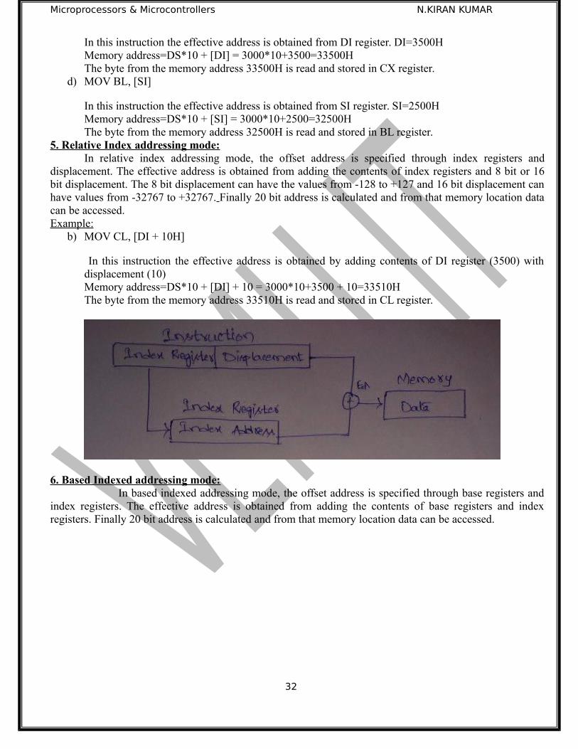
5. Relative Index addressing mode:In relative index addressing mode, the offset address is specified through index registers and
displacement. The effective address is obtained from adding the contents of index registers and 8 bit or 16bit displacement. The 8 bit displacement can have the values from -128 to +127 and 16 bit displacement canhave values from -32767 to +32767. Finally 20 bit address is calculated and from that memory location datacan be accessed.Example:
b) MOV CL, [DI + 10H]
In this instruction the effective address is obtained by adding contents of DI register (3500) withdisplacement (10)Memory address=DS*10 + [DI] + 10 = 3000*10+3500 + 10=33510HThe byte from the memory address 33510H is read and stored in CL register.
6. Based Indexed addressing mode:In based indexed addressing mode, the offset address is specified through base registers and
index registers. The effective address is obtained from adding the contents of base registers and indexregisters. Finally 20 bit address is calculated and from that memory location data can be accessed.
32

Microprocessors & Microcontrollers N.KIRAN KUMAR
Example:a) MOV AX, [BX + SI]
In this instruction the effective address is obtained by adding contents of BX register (2000) and SIregister (2500).Memory address=DS*10 + [BX] + [SI] = 3000*10+2000 + 2500=34500HThe byte from the memory address 34500H is read and stored in AX register.
7. Relative Based Indexed addressing mode:In relative based indexed addressing mode, the offset address is specified through base
registers, index registers and displacement. The effective address is obtained from adding the contents ofbase registers, index registers and displacement. Finally 20 bit address is calculated and from that memorylocation data can be accessed.
Example:a) MOV AX, [BX + SI + 50 H]
In this instruction the effective address is obtained by adding contents of BX register (2000), SIregister (2500) and 50H.Memory address=DS*10 + [BX] + [SI] +50H= 3000*10+2000 + 2500 + 50=34550HThe byte from the memory address 34500H is read and stored in AX register.
33

Microprocessors & Microcontrollers N.KIRAN KUMAR
Program memory addressing modes:The program memory addressing modes are used with the JMP and CALL instructions. These
addressing modes are related to branching instructions, where the flow of control is transferred from onelocation to another location. The data can be accessed from memory based on control transfer.
Based on the control transfer there are two types of addressing modes, they are Intra segment addressing mode Inter segment addressing mode
Intra segment addressing mode:If the flow of control is transferred within the segment then it is said to be intra segment addressing
mode.There are two types of intra segment addressing modes, they are
Direct Intra segment addressing mode Indirect Intra segment addressing mode
Direct Intra segment addressing modeIn this addressing mode, the address to which the control is to be transferred lies within the same
segment in the instruction and appears directly in the instruction as an immediate displacement value. In thisaddressing mode the displacement is calculated relative to the contents of instruction pointer (IP).
The effective address to which control will be transferred is given by the sum of 8 or 16 bitdisplacement and current IP contents. In case of jump instruction, if displacement is 8 bit (-127 to +128)then it is short jump and if the displacement is 16 bits (-32678 to +32677) then it is long jump.Example:JMP SHORT LABELIn direct Intra segment addressing mode:
In this addressing mode, the address to which the control is to be transferred lies within thesame segment in the instruction and but it is passed indirectly in the instruction. In this addressing mode thebranch address is found as the contents of register or memory location.Example:JMP [BX]Inter segment addressing mode:
In this addressing mode the flow of control is transferred from one segment to another segment.There are two types of inter segment addressing modes. They are
Inter segment direct addressing mode Inter segment indirect addressing mode
Inter segment direct addressing modeIn this addressing mode, the flow of control is transferred from one segment to another segment and
it is specified directly in the instruction. The contents of CS and IP are specified directly in the instruction.Example:JMP 5000H, 2000HInter segment indirect addressing mode:
In this addressing mode, the flow of control is transferred from one segment to another segment andit is passed to instruction indirectly ie; the contents of memory block containing four bytes ie; IP (LSB), IP(MSB), CS (LSB), CS (MSB) sequentially.Example:JMP [BX]Stack memory addressing mode:
34
Microprocessors & Microcontrollers N.KIRAN KUMAR
The stack is used to hold data temporarily during program execution and also store the return addressfor procedures and interrupt service routines (ISR). The stack memory is a last in first out (LIFO) memory.Data are placed into stack using the PUSH instruction and taken out using the POP instruction. The CALLinstruction uses the stack to hold the return address for procedure and RET instruction is used to removereturn address from the stack.
The stack segment is maintained by two types of registers; they are pointer register and stacksegment register. Data is pushed into or popped from the stack as word. Whenever a word is pushed intostack, the higher order 8 bits are placed into memory location specified by SP and then the lower order bitsare placed into memory specified by SP. SP is decremented by two locations.
Since SP gets decremented for every push operation, the stack segment is said to be growingdownwards, as for push operations, data are stored in the lower memory addresses in stack segment.
Whenever a word is popped from stack, the lower order 8 bits of word are removed from memorylocation specified by SP and then the higher order bits are removed from memory specified by SP. SP isincremented by two locations.
Example:PUSH AXPUSH DSPOP ESPOP [BX]
Instruction Set of 8086
The 8086 instructions are categorized into the following main types.
i. Data Transfer / Copy Instructions ii. Flag transfer instructionsiii. Arithmetic and Logical Instructions iv. Branch Instructionsv. Loop Instructions vi. Machine Control Instructionsvii. Flag Manipulation Instructions viii. Shift and Rotate Instructions ix. String Instructions
Data Copy / Transfer Instructions:
MOV:
This instruction copies a word or a byte of data from some source to a destination. The destination can be a
register or a memory location. The source can be a register, a memory location, or an immediate number.
The general format of MOV instruction is MOV destination, source
Example:
MOV AX, BX
MOV AX, 5000H
MOV AX, [SI]
MOV AX, [2000H]
35
Microprocessors & Microcontrollers N.KIRAN KUMAR
MOV [734AH], BX
MOV DS, CX
MOV CL, [357AH]
PUSH: Push to Stack
This instruction pushes the contents of the specified register/memory location on to the stack. The
stack pointer is decremented by 2, after each execution of the instruction.
Example:
PUSH AX
PUSH DS
PUSH [5000H]
POP: Pop from Sack
This instruction when executed, loads the specified register/memory location with the contents of
the memory location of which the address is formed using the current stack segment and stack pointer. The
stack pointer is incremented by 2.
Example:
POP AX
POP DS
POP [5000H]
XCHG: Exchange byte or word
This instruction exchanges the contents of the specified source and destination operands. Exchange
instruction can exchange the contents of a register from the contents of a memory location. The source and
destination must be either byte or word.
Example:
XCHG [5000H], AX
XCHG BX, AX
XLAT: Translate byte using look-up table
The XLAT instruction is used to translate a byte in AL from one code to another code. The instruction
replaces a byte in AL register with the byte in the memory at [BX], which is one of the data items present in a
look up table.
Before XLAT instruction is executed, the look up table containing the desired codes must be put in data
segment and offset address of the starting location of the look up table is stored in BX. The code byte to be
36

Microprocessors & Microcontrollers N.KIRAN KUMAR
translated is put in AL. when XLAT is executed now; it adds the content of AL with BX to find the offset
address of the data in look up table. Further the byte in that offset address will be get copied to AL.
Example:
LEA BX, TABLE1
MOV AL, 04H
XLAT
IN: Copy a byte or word from specified port to accumulator.
The IN instruction copies data from a port to the AL or AX register. If 8 bit port is read, the data is stored
in AL and if 16 bit port is read, the data is stored in AX.
The IN instruction has two formats. They are fixed port and variable port.
In fixed port type IN instruction, the 8 bit address of the port is specified directly in the instruction. With this
form, any one of possible ports can be addressed.
Example:
IN AL, 03H
IN AX, 40H
For variable port type IN instruction, the port address is loaded into DX register before the IN instruction. Since
DX is 16 bit register, the port address can be any one of the number between 0000H to FFFF H. Hence 65536
ports can be able to address.
Example:
MOV DX, 0FE H
IN AL, DX
IN AX, DX
OUT: Copy a byte or word from accumulator specified port.
The OUT instruction transfers a byte from AL or a word from AX to specified port. Similar to IN
instruction, OUT instruction has two forms- fixed and variable ports.
Example:
OUT 03H, AL
OUT DX, AX
LEA: Load effective address of operand in specified register.
The general format of LEA instruction is LEA destination, source. This instruction loads the effective
address of the source operand into the destination operand.
Example:
37

Microprocessors & Microcontrollers N.KIRAN KUMAR
LEA BX, ADR
LEA SI, ADR [BX]
LDS: Load pointer to DS
This instruction loads DS register and the specified destination register in the instruction with the content of
memory location specified as a source in the instruction.
Example:
LDS BX, 5000H
LES: Load pointer to ES
This instruction loads ES register and the specified destination register in the instruction with the content of
memory location specified as a source in the instruction.
Example:
LES BX, 5000H
Flag transfer instructions:
LAHF: Load (copy to) AH with the low byte the flag register.
[AH] [Flags low byte]
This instruction copies the lower order byte of the flag register into AH.
SAHF: Stores (copy) AH register to low byte of flag register.
[Flags low byte] [AH]
This instruction stores the content of AH in lower order of the flag register.
PUSHF: Copy flag register to top of stack.
This instruction copies the flag register contents to stack.
POPF: Copy word at top of stack to flag register.
This instruction copies the contents from stack to flag register.
Arithmetic Instructions:
The 8086 provides many arithmetic operations: addition, subtraction, negation, multiplication and
comparing two values.
ADD:
This instruction adds an immediate data or the contents of memory location specified in the register (source) to
the contents of another register (destination) or memory location. The result is in the destination. The source
and destination can be either register or memory location but can’t be both memory locations.
Example:
ADD AX, 0100H
ADD AX, BX
38

Microprocessors & Microcontrollers N.KIRAN KUMAR
ADD AX, [SI]
ADD AX, [5000H]
ADD [5000H], 0100H
ADC: Add with Carry
This instruction performs the same operation as ADD instruction, but adds the carry flag to the
result.
Example
ADC 0100H
ADC AX, BX
ADC AX, [SI]
ADC AX, [5000]
ADC [5000], 0100H
SUB: Subtract
The subtract instruction subtracts the source operand from the destination operand and the result is
left in the destination operand. The source and destination can be either register or memory location but can’t
be both memory locations.
Example:
SUB AX, 0100H
SUB AX, BX
SUB AX, [5000H]
SUB [5000H], 0100H
SBB: Subtract with Borrow
The subtract with borrow instruction subtracts the source operand and the borrow flag (CF) which
may reflect the result of the previous calculations, from the destination operand
Example:
SBB AX, 0100H
SBB AX, BX
SBB AX, [5000H]
SBB [5000H], 0100H
INC: Increment
39

Microprocessors & Microcontrollers N.KIRAN KUMAR
This instruction increases the contents of the specified Register or memory location by 1. Immediate
data cannot be operand of this instruction.
Example
INC AX
INC [BX]
INC [5000H]
DEC: Decrement
The decrement instruction subtracts 1 from the contents of the specified register or memory location.
Example
DEC AX
DEC [5000H]
NEG: Negate
The negate instruction forms 2’s complement of the specified destination in the instruction. The
destination can be a register or a memory location. This instruction can be implemented by inverting each bit
and adding 1 to it.
Example
NEG AL
AL = 0011 0101 35H
Replace number in AL with its 2’s complement
AL = 1100 1011 = CBH
CMP: Compare
This instruction compares the source operand, which may be a register or an immediate data or a
memory location, with a destination operand that may be a register or a memory location. For comparison, it
subtracts the source operand from destination operand but it does not store the result in destination.
Example
CMP BX, 0100H
CMP AX, 0100H
CMP [5000H], 0100H
CMP BX, [SI]
CMP BX, CX
MUL: Unsigned Multiplication Byte or Word
40

Microprocessors & Microcontrollers N.KIRAN KUMAR
This instruction multiplies an unsigned byte in source with unsigned byte in AL or multiplies
unsigned word in source with unsigned word in AX. The source can be either register or memory location. The
result will be stored in AX or DX register.
Example
MUL BH
MUL [DI]
IMUL: Signed Multiplication
This instruction multiplies a signed byte in source operand by a signed byte in AL or a signed word
in source operand by a signed word in AX. The source can be either register or memory location. The result is
stored in AX or DX.
Example
IMUL BH
IMUL CX
IMUL [SI]
CBW: Convert Signed Byte to Word
This instruction copies the sign of a byte in AL to all the bits in AH. AH is then said to be sign
extension of AL.
Example
MOV AX, 4255H AH=42, AL=55
CBW AX=0055 H
In this example, AL=55H is equivalent to 01010101H which means sign bit is 0. Hence after CBW the
sign bit is extended in to AH register. So AH=0055H.
CWD: Convert Signed Word to Double Word
This instruction sets all the bits in DX register to the same sign bit of AX register.
Example
MOV DX, 0000H, 0000 0000 0000 0000
MOV AX, F4ECH, 1111 0100 1110 1100
CWD
Result: DX = 1111 1111 1111 1111
In the above example, the sign bit in AX is 1 so the signed bit is extended to DX register. So DX=1111
1111 1111 1111
DIV: Unsigned division
41
Microprocessors & Microcontrollers N.KIRAN KUMAR
This instruction is used to divide an unsigned word by a byte. The word must be AX and byte can be
from a register or memory location. The quotient is stored in AL and remainder is stored in AH.
This instruction is used to divide an unsigned double word by a word. The double word must be AX or DX
and word can be from a register or memory location. The quotient is stored in AX and remainder is stored in
DX.
Example
DIV CL ; Word in AX / byte in CL ;
Quotient in AL, remainder in AH
DIV CX ; Double word in DX and AX / word in CX, and Quotient in AX, remainder in DX
ASCII & BCD Instructions
Representation of decimal numbers is
ASCII representationBCD representation
Unpacked BCD Packed BCD
ASCII:
When a number is entered in keyboard, microprocessor accepts data in form of ASCII values. For 0 to 9
decimal digits the corresponding ASCII values are 30 to 39. 8086 allows adding these data as they enter the
processor for decimal digits. For example, if 5 and 9 are entered through keyboard, 8086 accepts the data as
35 and 39 ASCII values.
For processing ASCII numbers the following instructions are used
ASCII addition (AAA) ASCII subtraction (AAS) ASCII multiplication (AAM) ASCII division (AAD)
For processing BCD numbers the following instructions are used
Packed BCD addition (DAA) Packed BCD subtraction (DAS)
AAA: ASCII Adjust After Addition
The AAA instruction is executed after an ADD instruction that adds two ASCII coded operand to
give a byte of result in AL. The AAA instruction converts the resulting contents of Al to unpacked decimal
digits. After the addition, the AAA instruction examines the lower 4 bits of AL to check whether it contains
42
Microprocessors & Microcontrollers N.KIRAN KUMAR
valid BCD number in the range 0 to 9 and if it is greater than 9, then 6 is added to it and AH is cleared. If carry
is generated it is added to AH.
AAS: ASCII Adjust AL after Subtraction
This instruction corrects the result in AL register after subtracting two unpacked ASCII operands.
The result is in unpacked decimal format. The procedure is similar to AAA instruction except for the
subtraction of 06 from AL.
AAM: ASCII Adjust after Multiplication
This instruction, after execution, converts the product available In AL into unpacked BCD format.
The AAM instruction, multiplies the two unpacked BCD operands and result is stored in AX.
AAD: ASCII Adjust before Division
This instruction converts two unpacked BCD digits in AH and AL to the equivalent binary number in
AL. This adjustment must be made before dividing the two unpacked BCD digits in AX by an unpacked BCD
byte. In the instruction sequence, this instruction appears Before DIV instruction.
DAA: Decimal Adjust Accumulator
This instruction is used to convert the result of the addition of two packed BCD numbers to a valid
BCD number. The result has to be only in AL. If the lower nibble is greater than 9, after addition or AF is set, it
will add 6 to lower nibble in AL. after adding 6 to lower nibble of AL, if the upper nibble of AL is greater than
9 or carry flag is set, DAA adds 60 to AL.
DAS: Decimal Adjust after Subtraction
This instruction converts the result of the subtraction of two packed BCD numbers to a valid BCD
number. The subtraction has to be in AL only. If the lower nibble is greater than 9, after subtraction or AF is set,
it will subtracts 6 to lower nibble in AL. after subtracting 6 to lower nibble of AL, if the upper nibble of AL is
greater than 9 or carry flag is set, DAA subtracts 60 to AL.
Logical Instructions
AND: Logical AND
This instruction bit by bit ANDs the source operand that may be an immediate register or a memory
location to the destination operand that may a register or a memory location. The result is stored in the
destination operand.
Example
AND AX, 0008H
AND AX, BX
OR: Logical OR
43
Microprocessors & Microcontrollers N.KIRAN KUMAR
This instruction bit by bit ORs the source operand that may be an immediate, register or a memory
location to the destination operand that may a register or a memory location. The result is stored in the
destination operand.
Example
OR AX, 0008H
OR AX, BX
NOT: Logical Invert
This instruction complements the contents of an operand register or a memory location, bit by bit.
Example
NOT AX
NOT [5000H]
XOR: Logical Exclusive OR
This instruction bit by bit XORs the source operand that may be an immediate, register or a memory
location to the destination operand that may a register or a memory location. The result is stored in the
destination operand.
Example
XOR AX, 0098H
XOR AX, BX
TEST: Logical Compare Instruction
The TEST instruction performs a bit by bit logical AND operation on the two operands. The result of
this ANDing operation is not available for further use, but flags are affected.
Example
TEST AX, BX
TEST [0500], 06H
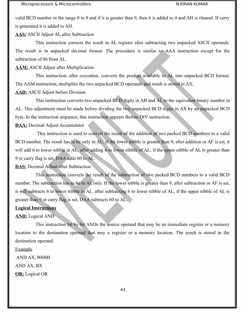
SAL/SHL: SAL / SHL destination, count.
SAL and SHL are two mnemonics for the same instruction. This instruction shifts each bit in the
specified destination to the left and 0 is stored at LSB position. The MSB is shifted into the carry flag. The
destination can be a byte or a word. It can be in a register or in a memory location. The number of shifts is
indicated by count.
44
Microprocessors & Microcontrollers N.KIRAN KUMAR
Example
SAL CX, 1
SAL AX, CL
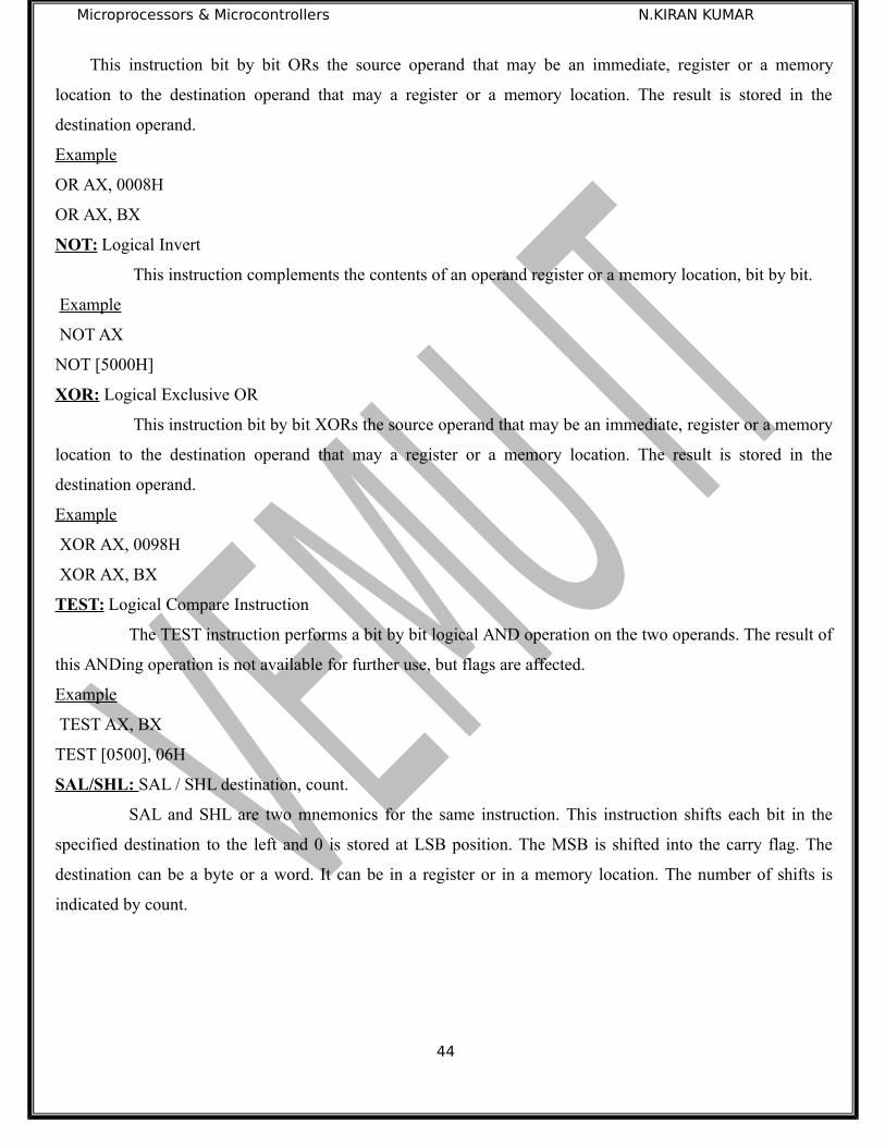
SHR: SHR destination, count
This instruction shifts each bit in the specified destination to the right and 0 is stored at MSB
position. The LSB is shifted into the carry flag. The destination can be a byte or a word. It can be a register or
in a memory location. The number of shifts is indicated by count.
Example
SHR CX, 1
MOV CL, 05H
SHR AX, CL
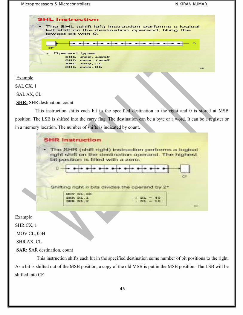
SAR: SAR destination, count
This instruction shifts each bit in the specified destination some number of bit positions to the right.
As a bit is shifted out of the MSB position, a copy of the old MSB is put in the MSB position. The LSB will be
shifted into CF.
45
Microprocessors & Microcontrollers N.KIRAN KUMAR
Example
SAR BL, 1
MOV CL, 04H
SAR DX, CL
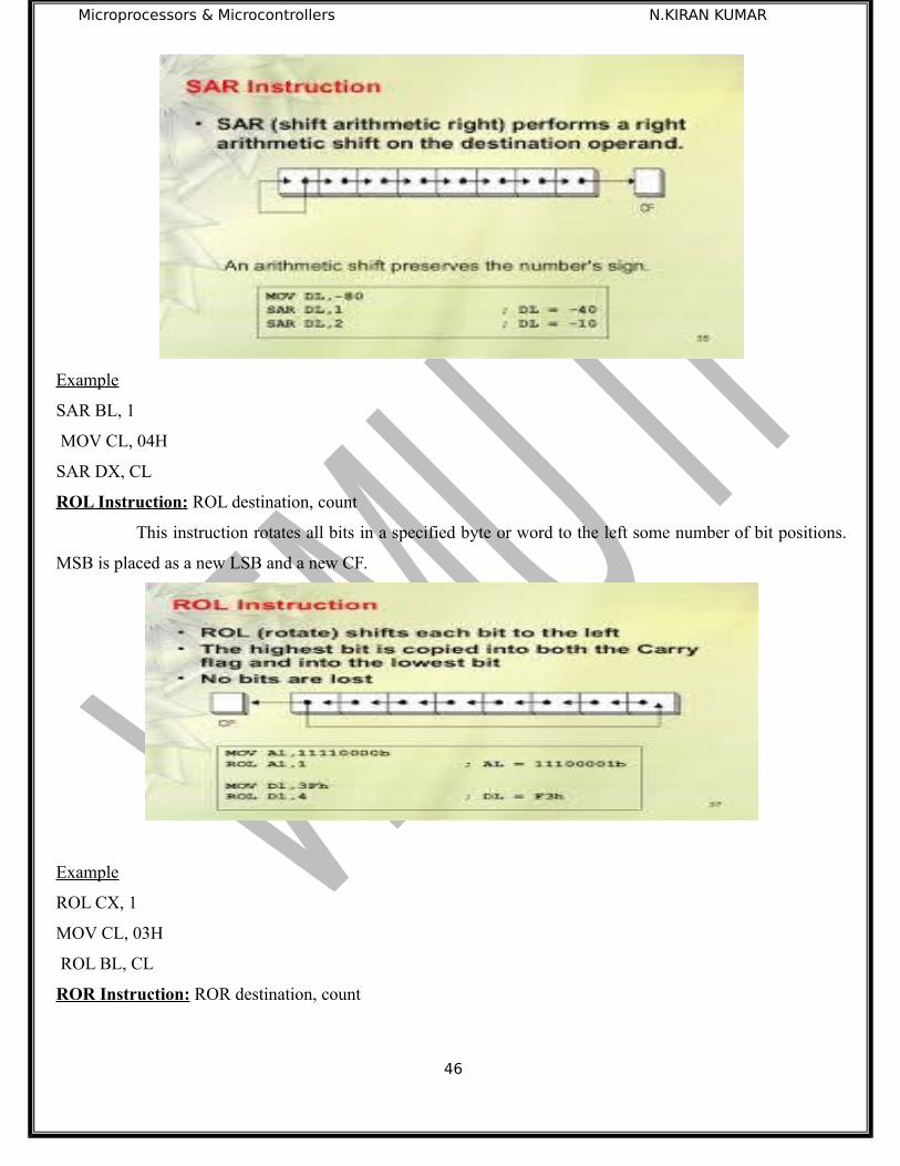
ROL Instruction: ROL destination, count
This instruction rotates all bits in a specified byte or word to the left some number of bit positions.
MSB is placed as a new LSB and a new CF.
Example
ROL CX, 1
MOV CL, 03H
ROL BL, CL
ROR Instruction: ROR destination, count
46
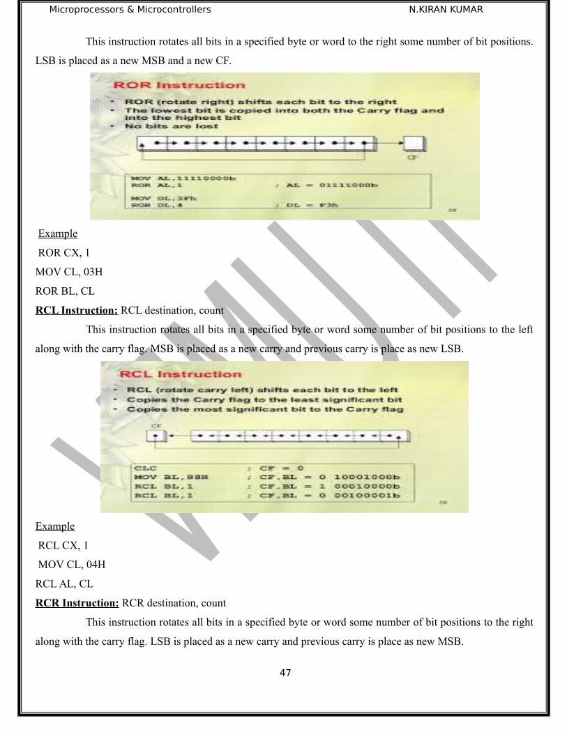
Microprocessors & Microcontrollers N.KIRAN KUMAR
This instruction rotates all bits in a specified byte or word to the right some number of bit positions.
LSB is placed as a new MSB and a new CF.
Example
ROR CX, 1
MOV CL, 03H
ROR BL, CL
RCL Instruction: RCL destination, count
This instruction rotates all bits in a specified byte or word some number of bit positions to the left
along with the carry flag. MSB is placed as a new carry and previous carry is place as new LSB.
Example
RCL CX, 1
MOV CL, 04H
RCL AL, CL
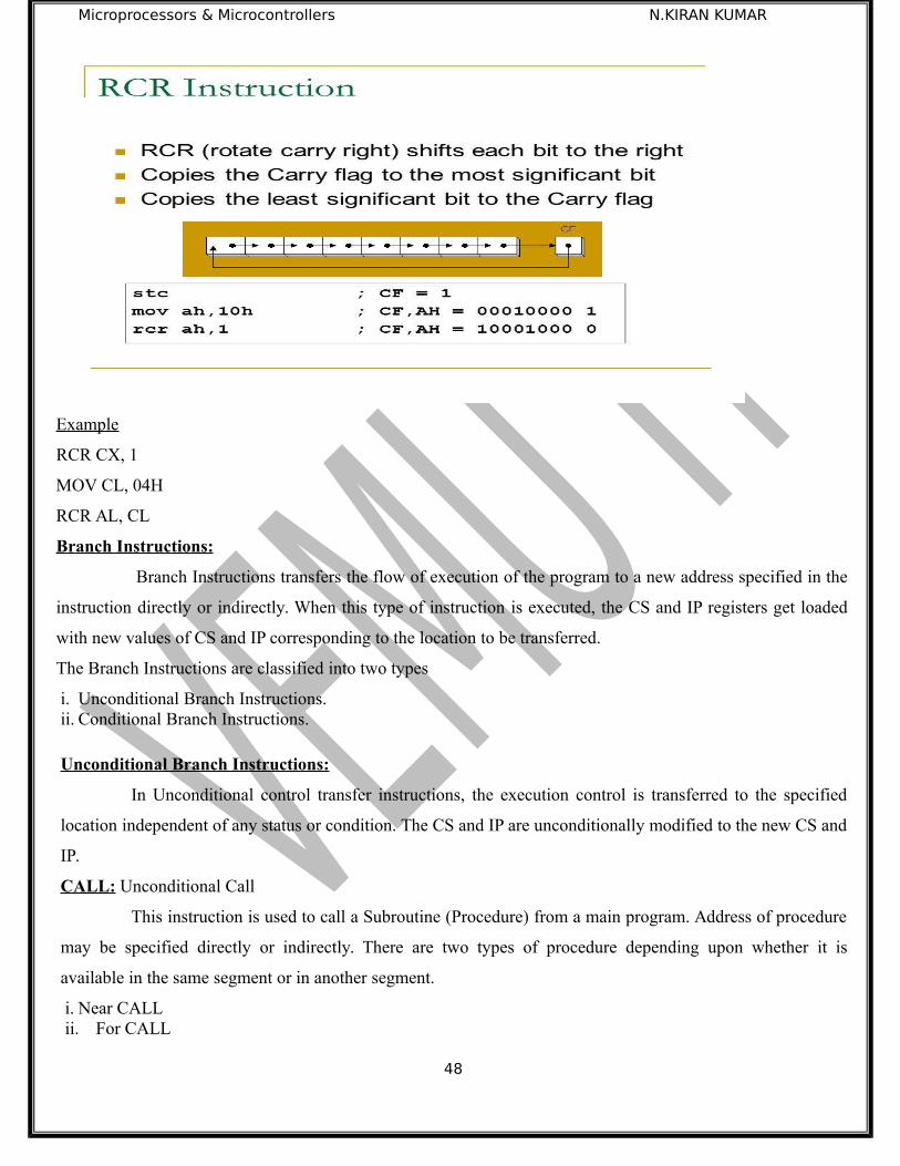
RCR Instruction: RCR destination, count
This instruction rotates all bits in a specified byte or word some number of bit positions to the right
along with the carry flag. LSB is placed as a new carry and previous carry is place as new MSB.
47
Microprocessors & Microcontrollers N.KIRAN KUMAR
Example
RCR CX, 1
MOV CL, 04H
RCR AL, CL
Branch Instructions:
Branch Instructions transfers the flow of execution of the program to a new address specified in the
instruction directly or indirectly. When this type of instruction is executed, the CS and IP registers get loaded
with new values of CS and IP corresponding to the location to be transferred.
The Branch Instructions are classified into two types
i. Unconditional Branch Instructions. ii. Conditional Branch Instructions.
Unconditional Branch Instructions:
In Unconditional control transfer instructions, the execution control is transferred to the specified
location independent of any status or condition. The CS and IP are unconditionally modified to the new CS and
IP.
CALL: Unconditional Call
This instruction is used to call a Subroutine (Procedure) from a main program. Address of procedure
may be specified directly or indirectly. There are two types of procedure depending upon whether it is
available in the same segment or in another segment.
i. Near CALL ii. For CALL
48

Microprocessors & Microcontrollers N.KIRAN KUMAR
On execution this instruction stores the incremented IP & CS onto the stack and loads the CS & IP
registers with segment and offset addresses of the procedure to be called.
RET: Return from the Procedure.
At the end of the procedure, the RET instruction must be executed. When it is executed, the
previously stored content of IP and CS along with Flags are retrieved into the CS, IP and Flag registers from
the stack and execution of the main program continues further.
INT N: Interrupt Type N.
In the interrupt structure of 8086, 256 interrupts are defined corresponding to the types from 00H to
FFH. When INT N instruction is executed, the type byte N is multiplied by 4 and the contents of IP and CS of
the interrupt service routine will be taken from memory block in 0000 segment.
INTO: Interrupt on Overflow
This instruction is executed, when the overflow flag OF is set. This is equivalent to a Type 4
Interrupt instruction.
JMP: Unconditional Jump
This instruction unconditionally transfers the control of execution to the specified address using an
8-bit or 16-bit displacement. No Flags are affected by this instruction.
IRET: Return from ISR
When it is executed, the values of IP, CS and Flags are retrieved from the stack to continue the
execution of the main program.
LOOP: LOOP Unconditionally
This instruction executes the part of the program from the Label or address specified in the
instruction up to the LOOP instruction CX number of times. After each iteration, CX is decremented
automatically and JUMP IF NOT ZERO structure.
Conditional Branch Instructions
When this instruction is executed, execution control is transferred to the address specified relatively
in the instruction, provided the condition implicit in the op code is satisfied. Otherwise execution continues
sequentially.
JZ/JE Label Transfer execution control to address ‘Label’, if ZF=1.
JNZ/JNE Label Transfer execution control to address ‘Label’, if ZF=0
JS Label Transfer execution control to address ‘Label’, if SF=1.
JNS Label Transfer execution control to address ‘Label’, if SF=0.
JO Label Transfer execution control to address ‘Label’, if OF=1.
JNO Label Transfer execution control to address ‘Label’, if OF=0.
49
Microprocessors & Microcontrollers N.KIRAN KUMAR
JNP Label Transfer execution control to address ‘Label’, if PF=0.
JP Label Transfer execution control to address ‘Label’, if PF=1.
JB Label Transfer execution control to address ‘Label’, if CF=1.
JNB Label Transfer execution control to address ‘Label’, if CF=0.
JCXZ Label Transfer execution control to address ‘Label’, if CX=0
Conditional LOOP Instructions
LOOPZ / LOOPE Label
Loop through a sequence of instructions from label while ZF=1 and CX=0.
LOOPNZ / LOOPENE
Label Loop through a sequence of instructions from label while ZF=1 and CX=0.
String Manipulation Instructions
A series of bytes or words available in memory at consecutive locations is referred as String byte or
String word. A String of characters may be located in consecutive memory locations, where each character
may be represented by its ASCII equivalent.
The 8086 supports a set of more powerful instructions for string manipulations for referring to a
string, two parameters are required.
I. Starting and End Address of the String. II. Length of the String.
The length of the string is usually stored as count in the CX register. The incrementing or
decrementing of the pointer, in string instructions, depends upon the Direction Flag (DF) Status. If it is a
Byte string operation, the index registers are updated by one. On the other hand, if it is a word string
operation, the index registers are updated by two.
REP: Repeat Instruction Prefix
This instruction is used as a prefix to other instructions, the instruction to which the REP prefix is provided,
is executed repeatedly until the CX register becomes zero (at each iteration CX is automatically
decremented by one).
i. REPE / REPZ - repeat operation while equal / zero. ii. REPNE / REPNZ - repeat operation while not equal / not zero. These are used for CMPS, SCAS
instructions only, as instruction prefixes.
MOVSB / MOVSW: Move String Byte or String Word
50

Microprocessors & Microcontrollers N.KIRAN KUMAR
Suppose a string of bytes stored in a set of consecutive memory locations is to be moved to another
set of destination locations. The starting byte of source string is located in the memory location whose
address may be computed using SI (Source Index) and DS (Data Segment) contents. The starting address of
the destination locations where this string has to be relocated is given by DI (Destination Index) and ES
(Extra Segment) contents.
CMPS: Compare String Byte or String Word
The CMPS instruction can be used to compare two strings of byte or words. The length of the string
must be stored in the register CX. The contents of source location are subtracted from the destination
location when CMP instruction is executed. If both the byte or word strings are equal, zero Flag is set. The
REP instruction Prefix is used to repeat the operation till CX (counter) becomes zero or the condition
specified by the REP Prefix is False.
SCAN: Scan String Byte or String Word
This instruction scans a string of bytes or words for an operand byte or word specified in the register
AL or AX. The String is pointed to by ES: DI register pair. The length of the string is stored in CX. The DF
controls the mode for scanning of the string. Whenever a match to the specified operand is found in the
string, execution stops and the zero Flag is set. If no match is found, the zero flag is reset.
LODS: Load String Byte or String Word
The LODS instruction loads the AL / AX register by the content of a string pointed to by DS: SI
register pair. The SI is modified automatically depending upon DF, if it is a byte transfer (LODSB), the SI is
modified by one and if it is a word transfer (LODSW), the SI is modified by two. No other Flags are
affected by this instruction.
STOS: Store String Byte or String Word
The STOS instruction Stores the AL / AX register contents to a location in the string pointer by ES:
DI register pair. The DI is modified accordingly; No Flags are affected by this instruction.
The direction Flag controls the String instruction execution, the source index SI and Destination
Index DI are modified after each iteration automatically. If DF=1, then the execution follows auto decrement
mode, SI and DI are decremented automatically after each iteration. If DF=0, then the execution follows
auto increment mode. In this mode, SI and DI are incremented automatically after each iteration.
51
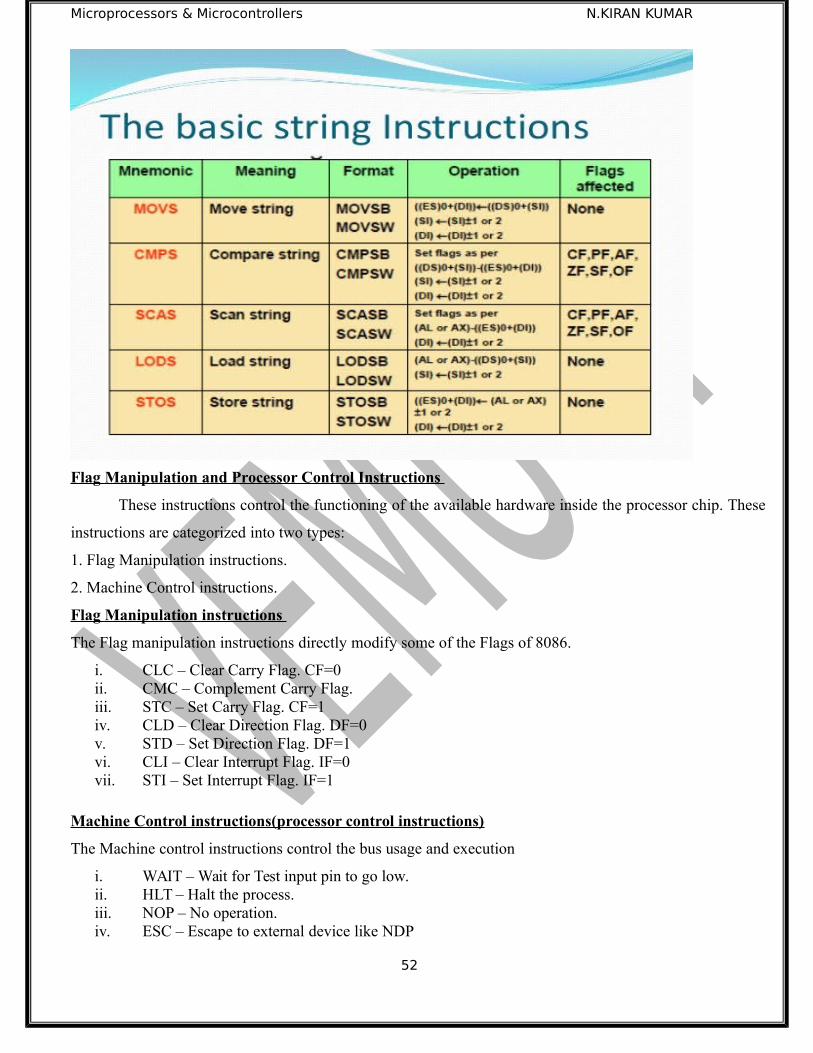
Microprocessors & Microcontrollers N.KIRAN KUMAR
Flag Manipulation and Processor Control Instructions
These instructions control the functioning of the available hardware inside the processor chip. These
instructions are categorized into two types:
1. Flag Manipulation instructions.
2. Machine Control instructions.
Flag Manipulation instructions
The Flag manipulation instructions directly modify some of the Flags of 8086.
i. CLC – Clear Carry Flag. CF=0ii. CMC – Complement Carry Flag. iii. STC – Set Carry Flag. CF=1iv. CLD – Clear Direction Flag. DF=0 v. STD – Set Direction Flag. DF=1vi. CLI – Clear Interrupt Flag. IF=0vii. STI – Set Interrupt Flag. IF=1
Machine Control instructions(processor control instructions)
The Machine control instructions control the bus usage and execution
i. WAIT – Wait for Test input pin to go low. ii. HLT – Halt the process. iii. NOP – No operation. iv. ESC – Escape to external device like NDP
52

Microprocessors & Microcontrollers N.KIRAN KUMAR
v. LOCK – Bus lock instruction prefix
WAIT Instruction:When WAIT instruction is executed it takes microprocessor to idle condition. The CPU will not
do any processing during this condition, until TEST pin becomes low or interrupt is received on INTR orNMI pin.
HLT Instruction:When ever HLT instruction is executed, it causes 8086 to stop fetching and executing instructions.
The 8086 will enter into halt state. The only way to get the processor out of halt state is the interruptsignal on INTR pin or interrupt signal on NMI pin or reset signal on RESET input.NOP Operation:
This instruction simply takes three clock cycles and does no processing. After this it will executethe next instruction. This instruction is used to provide delay between two instructions.ESC Instruction:
When ever this instruction is executed the microprocessor passes the information to othercoprocessor.LOCK Instruction:
This instruction is used as prefix. This prefix makes sure that during execution of the instruction,control of system is not taken by other microprocessor. It prevents the access of system bus from others.Assembly language programming:
Assembly language programs can be converted into machine language programs either bymanually finding the op code for each instruction in the program or by using assembler and executing in8086 based systems.
Since manually finding the op code of each instruction of 8086 is time consuming, the assembleris normally used to converting assembly language programs to machine language programs.
Many assemblers, such as Microsoft Macro Assembler (MASM), Turbo Assembler (TASM), andDOS Assembler are used to convert the 8086 assembly language programs into machine languageprograms.
While using these assemblers, the assembly language program is written using assemblerdirectives. Assembler directives are the commands to the assembler to indicate the size of variable,number of bytes or words to be reserved in the memory, value of a constant, name of the segment, etc., inthe program. Assembler directives are the alphabet strings which are given to the assembler as hints or directions whileconverting assembly language programming to machine language programming.There are two types of statements in an assembly language programming. They are
1. Instructions: These are translated into object codes by the assembler.2. Directives: These give directions to the assembler during assembly process.
Types of assemblers:There are two types of assemblers. They are
One pass assembler: The assembler scans the program statements one by one from left to right
starting with first statement to last statement indicated by end statement. This is called the pass.The purpose of first pass is to provide the assembler the location of labels.
Two pass assembler: The assembler scans the program statements twice. The first scan consists
of labels of addresses. The second scan translates the assembly program to binary codes.
Assembly language program development tools:
53
Microprocessors & Microcontrollers N.KIRAN KUMAR
Editor:An editor is a program which allows creating the file containing the assembly language
statements. The assembly programs are saved as .ASM file.Assembler:
An assembler is a program used to translate assembly language programs to machine languageprograms. It produces . OBJ file.Linker:
A linker is a program used to join several file into large object file. It produces . EXE file so thatthe program becomes executable.Locator:A locator is a program which is used to assign the specific address of where the segments of object codeare to be loaded into memory. It converts .EXE file to .BIN file.Debugger:
A debugger is a program which allows loading .OBJ code program into system memory,executing program and troubleshooting.
Emulator:An emulator is a mixture of hardware and software. It is used to test and debug the hardware and
software of external system.Assembler Directives
In assembly language programming while converting assembly language program to machinelanguage some errors may occur. To overcome these errors hints or directions are to be given to theassembler. These directions or hints are given through Assembler directives.Assembler directives are alphabet strings which are given to assembler as directions.DB - Defined Byte. DD - Defined Double WordDQ - Defined Quad Word DT - Define Ten Bytes DW - Define WordDB - DB directive is used to declare a byte type variable or to store a byte in memory location.Example:1. PRICE DB 49h, 98h, 29h ;
Declare an array of 3 bytes, named as PRICE and initialize.2. NAME DB ‘ABCDEF’ ;
Declare an array of 6 bytes and initialize with ASCII code for letters 3. TEMP DB 100 DUP(?) ;
Set 100 bytes of storage in memory and give it the name as TEMP, but leave the 100 bytesuninitialized. Program instructions will load values into these locations.
DW - The DW directive is used to define a variable of type word or to reserve storage location of typeword in memory. Example: MULTIPLIER DW 437Ah; This declares a variable of type word and named it as MULTIPLIER. This variable is initialized with thevalue 437Ah when it is loaded into memory to run. EXP1 DW 1234h, 3456h, 5678h ; this declares an array of 3 words and initialized with specified values.
54

Microprocessors & Microcontrollers N.KIRAN KUMAR
STOR1 DW 100 DUP (0); Reserve an array of 100 words of memory and initialize all words with 0000.Array is named as STOR1.DD - The DW directive is used to define a variable of type double word or to reserve storage location oftype double word in memory. DQ - The DW directive is used to define a variable of type quad word or to reserve storage location oftype quad word in memory. DT - The DW directive is used to define a variable of type ten words or to reserve storage location oftype ten words in memory. END - END directive is placed after the last statement of a program to tell the assembler that this is theend of the program module. The assembler will ignore any statement after an END directive. Carriagereturn is required after the END directive. ENDP - ENDP directive is used along with the name of the procedure to indicate the end of a procedureto the assembler Example: SQUARE_NUM PROCE; It start the procedure some steps to find the square root of a number SQUARE_NUM ENDP Hear it is the End for the procedure ENDS - This ENDS directive is used with name of the segment to indicate the end of that logic segment. Example: CODE SEGMENT;Hear it start the logic segment containing code. Some instructions statements to perform the logicaloperation CODE ENDS;End of segment named as CODE EVEN - This EVEN directive instructs the assembler to increment the location of the counter to the nexteven address if it is not already in the even address. If the word is at even address 8086 can read amemory in 1 bus cycle. If the word starts at an odd address, the 8086 will take 2 bus cycles to get thedata. A series of words can be read much more quickly if they are at even address. When EVEN is usedthe location counter will simply incremented to next address and NOP instruction is inserted in thatincremented location. Example: DATA1 SEGMENT; Location counter will point to 0009 after assembler reads next statement SALES DB 9 DUP(?);Declare an array of 9 bytes EVEN increment location counter to 000AH RECORD DW 100 DUP( 0 );Array of 100 words will start from an even address for quicker read DATA1 ENDS EQU - This EQU directive is used to give a name to some value or to a symbol. Each time the assemblerfinds the name in the program, it will replace the name with the value or symbol you given to that name. Example: FACTOR EQU 03H;ASSUME The ASSUME directive is used to tell the assembler that the name of the logical segment should be usedfor a specified segment. The 8086 works directly with only 4 physical segments: a Code segment, a datasegment, a stack segment, and an extra segment. Example: ASUME CS: CODE This tells the assembler that the logical segment named CODE contains the instruction statements for theprogram and should be treated as a code segment.
55

Microprocessors & Microcontrollers N.KIRAN KUMAR
ASUME DS: DATA This tells the assembler that for any instruction which refers to a data in the data segment, data will foundin the logical segment DATA. GROUP - The GROUP directive is used to group the logical segments named after the directive into onelogical group segment. LABLE- This directive indicates that name is assigned to the current memory location.NAME- This directive indicates the name given to the program module.OFFSET – This directive determines offset address of the segment.INCLUDE - This INCLUDE directive is used to insert a block of source code from the named file intothe current source module. ORG- This directive is used to indicate the starting memory location of the program.PROC - The PROC directive is used to identify the start of a procedure. The term near or far is used tospecify the type of the procedure. Example: SMART PROC FAR;
This identifies that the start of a procedure named as SMART and instructs the assembler thatthe procedure is far. SMART ENDP
This PROC is used with ENDP to indicate the break of the procedure. PTR - This PTR operator is used to declare the type of label, variable, or memory operand. The operatorPTR is prefixed by either BYTE or WORD. If the prefix is BYTE, particular label, variable, or memoryoperand is treated as an 8 bit quantity, while if the prefix is WORD, it is treated as 16 bit quantity.Example: INC BYTE PTR [BX];
Increment the byte pointed to by BX. This PTR operator can also be used to override thedeclared type of variable. SEGMENT- This directive indicates the start of the logical segment.PUBLIC - The PUBLIC directive is used to instruct the assembler that a specified name or label will beaccessed from other modules. Example: PUBLIC DIVISOR, DIVIDEND;These two variables are public so these are available to all modules. If an instruction in a module refers toa variable in another assembly module, we can access that module by declaring as EXTRN directive. SHORT – This type of directive tells assembler that only 1 byte of displacement is required to jumpinstruction.Example:JMP SHORT MULTIPLYTYPE - TYPE operator instructs the assembler to determine the type of a variable and determines thenumber of bytes specified to that variable. Example: Byte type variable – assembler will give a value 1 Word type variable – assembler will give a value 2 Double word type variable – assembler will give a value 4 ADD BX, TYPE WORD_ ARRAY; MACRO and ENDM:
Suppose a number of instructions occur repeatedly in the main program, the program becomeslengthy. In such situations a macro definition is assigned with repeatedly appearing string of instructions.The process of assigning a label or macro name to repeatedly appearing string of instructions is called
56
Microprocessors & Microcontrollers N.KIRAN KUMAR
macro definition. The macro name is then used throughout the main program to refer to that string ofinstructions.A MACRO can be defined anywhere in a program, using the directive MACRO and ENDM. The ENDMdirective marks the end of the instructions or statements assigned to macro name.EXTRN and PUBLIC:
The directive EXTRN (external) informs the assembler that the procedures, labels, and namesdeclared after this directive have already been defined in some other segments and in the segments wherethey actually appear, they must be declared public, using public directive.
LOCAL:The label, variables, constants or procedures declared LOCAL in a module are to be used only
by that particular module.Global:
The label, variables, constants or procedures declared GLOBAL in a module are to be used byother modules of the program.Modular programming
In a program it may be necessary to perform a particular a task repeatedly. The formulation ofcomplex programs from number of complex sequences called program modules which performs a welldefined task is referred as modular programming.
Large programs are broken into small segments called modules. Each module implements aspecific function and has its own code segment and data segment.
Procedures are useful in such situations. A procedure is a group of instructions that usuallyperforms a task. It forms a reusable section of software which is stored once in memory. This savesmemory space and makes it easier to develop the software. A procedure is a sequence of instructions,which can be employed repeatedly within a longer program.
To make software development faster, it is better to develop and test in the form of smallprogram segments. This splitting does not cause any loss of capability to the program. The advantages ofprocedures over single programs are-
1. It reduces the code length and memory requirement2. It reduces development time as the modifications in the procedures are localized, which can be
debugged and tested separately.3. It supports modular programming methodology and improves the legibility of a programs the flow
of logic is well defined.4. Since it is possible to develop library of procedures for most commonly used task, which can be
shared by users from library, unnecessary duplication of codes can be avoided. A list of librarymodules may be only requirement for the user.
5. Procedure provides a flexible and convenient way of exchanging information between theapplication programs.
In order to handle procedures, operations required by the processor systems are invoking orcalling a procedure ( called program) and returning from the module back to main program ( callingprogram).
It is necessary to provide the input parameters to the procedure when it is called and to returnback to the result after execution. The number of input/output parameters passed to and from theprocedure can vary. Even the parameters to be passed may be control/status information which maynot have peripheral for data transfer.
57

Microprocessors & Microcontrollers N.KIRAN KUMAR
Since the main module and procedure use processor registers/RAM without any difference,they can be used to hold the input as well as output parameter information. If data is small in amountto exchange there is no problem but if large amount of data is to be exchanged then information mustbe stored in memory location and it is necessary to pass address pointer to the module. To reduce thisproblem, stack can be used for passing the parameter.The procedure may be classified as follows:
1. Intra segment procedure( Near procedure)2. Inter segment procedure ( Far procedure )3. Re – entrant procedure4. Recursive procedure
Intra segment procedure (Near procedure)These procedures defined in the same segment of the main program module. They can be
identified by near directive.Inter segment procedure (Far procedure)
These procedures are not defined in main program module but they are defined in othersegment. They can be identified by far directive.Re – entrant procedure
They define the procedure that can be interrupted, used and re entered without losing data.Recursive procedure
These procedures that can be called by themselves and are often used to work with complexdata structures called trees.The instructions that are used to handle the procedures:
1. CALL2. RET3. RETF4. RETN
CALL Instruction:When CALL instruction is executed, the instruction performs the following two operations:
1) Stores the return address to which the procedure will return to the execution.2) Modified the contents of instruction pointer register so that it points to the starting address of the
procedure, depending upon whether it is an intra segment or an inter segment call.
Types of CALL instructions:Direct CALL:
If the procedure is in the same segment then the processor produces the starting address of theprocedure by adding 16 bit displacement contained in the instruction to the contents of IP.
If the procedure is in another segment then IP and CS register contents are changed to transfercontrol to the procedure.In Direct CALL:
If the procedure is in the same segment then the processor produces the starting address of theprocedure by adding 16 bit value specified by any of the general purpose register in the instruction to thecontents of IP.
If the procedure is in another segment then it replaces IP and CS register contents with 16 bitvalues from memory locations whose address is specified by MOD type in the instruction.RET Instruction:
The RET instruction is the last instruction in the procedure. At the end of the procedure, thevalue saved in the stack is loaded back in the IP register to return execution to the calling program so that
58
Microprocessors & Microcontrollers N.KIRAN KUMAR
the control is transferred to the main program. The assembler will automatically code a near RET for anear procedure and a far RET for far procedure.RETF:
This instruction copies the return values from the stack back into the IP and CS registers totransfer control to next line in main program.RETN:
This instruction copies the return values from the stack back into the IP register.Macro
A macro is a group of instructions that performs a task. It is inserted in the program during theassembly process. Macro instructions are provided in the program by the assembler at a point where theyare invoked by using their names. A macro is a sequence of code that needs to be written only once butbasic structure can repeated several times within a module by giving its name.
The code to be repeated is called the prototype code, and the prototype code along with thestatements for referencing and terminating is called the macro definition. The procedure for using amacro is to give macro definition and then declare it at various appropriate points within a program byplacing the statement macro calls. When a macro is encountered by the assembler, the assembler replacesthe call with the macro’s code. It is proceed by a macro definition and completed by a macro terminator.
The macro and endm directives are used to define a macro sequence. The first statement of amacro contains the name and any parameters associated with it. It is termed as definition. The laststatement endm is called terminator. All the statements between name and terminator define a macrobody. When a macro is to be used its name is written. This is called macro call. The assembler replacesthe call with the code. This is called macro expansion.Example:PUSH_ALLMACRO ; Definition PUSH AX ; Macro bodyPUSH BXPUSH CXPUSH DXPUSH DIPUSH SIENDM ; TerminatorComparison between procedure and macro PROCEDURE MACRO
Procedures are called during programexecution
Macros are inserted during assemblyprocess
Procedures are assembled and executedseparately
Macros cannot be executed separately
Procedures reduces memoryrequirements
There will be no change in memoryrequirements for macros
Procedures can be defined anywhereand in any segment
Macros can be defined in the sameprogram
Procedure requires a special CALLstatement
Macros can be used just by using itsname
Procedure can be used by anyassembler
Macros can be used if assemblersupports MACRO features
In procedures parameters can be passedthrough registers and memory or stack
In macros parameters can passed as apart of the statement that calls MACRO
In procedure machine code is put only In macros machine code is generated59

Microprocessors & Microcontrollers N.KIRAN KUMAR
once in memory each time when it is called Procedures can be accessed by CALL
and RETURN mechanism duringprogram execution
Macros can be accessed duringassembly process when a name given toit is defined.
UNIT IIIIntroduction to microcontrollers
A microcontroller is a special digital processor system which is designed for specificapplication. Microcontroller is a single chip micro computer.
A microcomputer consists of digital computer and a microprocessor along with memory,I/O devices, CPU, I/O ports, timers/counters, ADC, DAC, serial ports, interrupt logic, oscillatorcircuit and functional blocks.
A microcontroller is a highly integrated single chip, which consists of on chip CPU(Central Processing Unit), RAM (Random Access Memory), EPROM/PROM/ROM (ErasableProgrammable Read Only Memory), I/O (input/output) – serial and parallel, timers, interruptcontroller.
S .No Microprocessor Microcontroller
1A microprocessor is a generalpurpose device which is a singleVLSI chip called a CPU.
A microcontroller is a dedicated chipwhich is also called single chip computer.
2
A microprocessor do not contain onchip I/O Ports, Timers, Memories etc.
A microcontroller includes RAM, ROM,serial and parallel interface, timers,interrupt circuitry (in addition to CPU) ina single chip.
3It has many instructions to move thedata between memory and CPU.
It has one or two instructions to move thedata between memory and CPU.
4Microprocessor instructions aremainly nibble or byte addressable
Microcontroller instructions are both bitaddressable as well as byte addressable.
5Access times for memory and I/Odevices are more.
Access times for built-in memory and I/Odevices are less.
6Microprocessor based system designis complex and expensive
Microcontroller based system design israther simple and cost effective
7Microprocessor based systemrequires more hardware.
Microcontroller based system requires lesshardware reducing PCB size andincreasing reliability.
8It has single memory for data andcode.
It has separate memory map for data andcode.
9Less number of pins aremultifunctional.
More number of pins are multifunctional.
60

Microprocessors & Microcontrollers N.KIRAN KUMAR
C omputer architectures
RISC and CISC CPU architectures
RISC CISC
Instruction takes one or two cycles Instruction takes multiple cycles
Only load/store instructions are used to accessmemory
In additions to load and store instructions,memory access is possible with otherinstructions also.
Instructions executed by hardware Instructions executed by the micro program
Fixed format instruction Variable format instructions
Few addressing modes Many addressing modes
Few instructions Complex instruction set
Most of the have multiple register banks Single register bank
Highly pipelined Less pipelined
Complexity is in the compiler Complexity in the micro program
Harvard & Von- Neumann CPU architecture
Von Neumann Architecture:
It is named after the mathematician and early computer scientist John Von Neumann.
The computer has single storage system (memory) for storing data as well as program to beexecuted.
It consists of a single set of address/data buses between CPU and memory
Processor needs two clock cycles to complete an instruction. Pipelining the instructions is notpossible with this architecture.
61
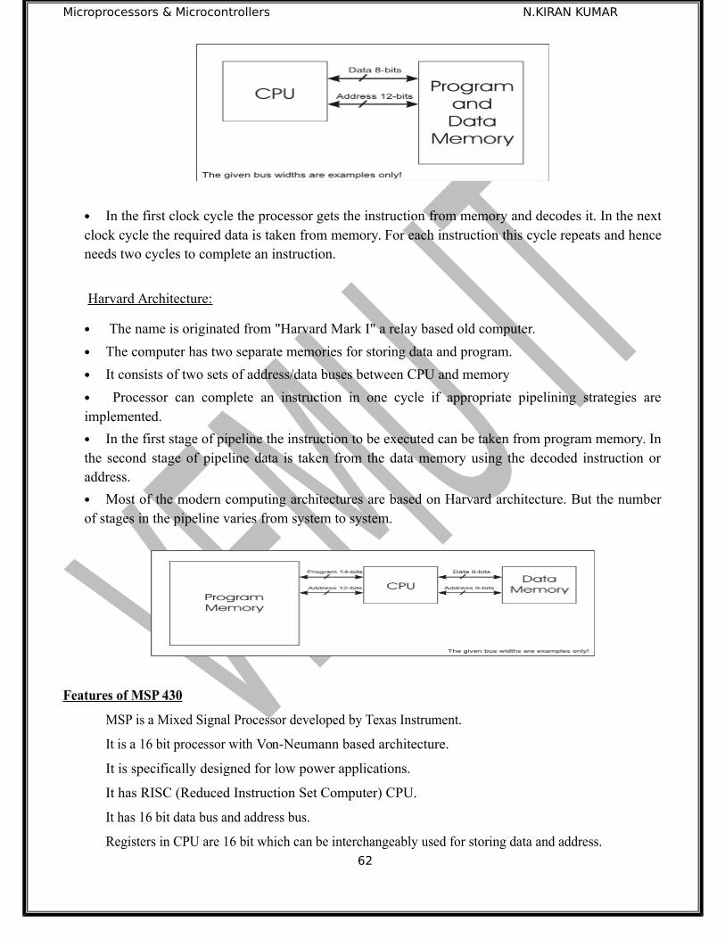
Microprocessors & Microcontrollers N.KIRAN KUMAR
In the first clock cycle the processor gets the instruction from memory and decodes it. In the nextclock cycle the required data is taken from memory. For each instruction this cycle repeats and henceneeds two cycles to complete an instruction.
Harvard Architecture:
The name is originated from "Harvard Mark I" a relay based old computer.
The computer has two separate memories for storing data and program.
It consists of two sets of address/data buses between CPU and memory
Processor can complete an instruction in one cycle if appropriate pipelining strategies areimplemented.
In the first stage of pipeline the instruction to be executed can be taken from program memory. Inthe second stage of pipeline data is taken from the data memory using the decoded instruction oraddress.
Most of the modern computing architectures are based on Harvard architecture. But the numberof stages in the pipeline varies from system to system.
Features of MSP 430
MSP is a Mixed Signal Processor developed by Texas Instrument.
It is a 16 bit processor with Von-Neumann based architecture.
It is specifically designed for low power applications.
It has RISC (Reduced Instruction Set Computer) CPU.
It has 16 bit data bus and address bus.
Registers in CPU are 16 bit which can be interchangeably used for storing data and address.62
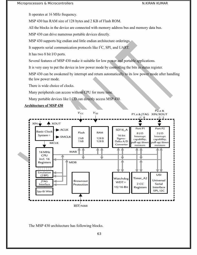
Microprocessors & Microcontrollers N.KIRAN KUMAR
It operates at 16 MHz frequency.
MSP 430 has RAM size of 128 bytes and 2 KB of Flash ROM.
All the blocks in the device are connected with memory address bus and memory data bus.
MSP 430 can drive numerous portable devices directly.
MSP 430 supports big endian and little endian architecture orderings.
It supports serial communication protocols like I2C, SPI, and UART.
It has two 8 bit I/O ports.
Several features of MSP 430 make it suitable for low power and portable applications.
It is very easy to put the device in low power mode by controlling the bits in status register.
MSP 430 can be awakened by interrupt and return automatically to its low power mode after handlingthe low power mode.
There is wide choice of clocks.
Many peripherals can access without CPU for more time.
Many portable devices like LCD can directly access MSP 430.
Architecture of MSP 430
The MSP 430 architecture has following blocks.
63
Microprocessors & Microcontrollers N.KIRAN KUMAR
Clock systemFlash memoryRAMCPUEmulationJTAG InterfaceSPY-Bi WireWatch dog timerBrown out protectionPortA/D converterUSI/SPI/I2CTimer registers
Clock systemThe clock system of MSP 430 provides three clocks namely Master clock (MCLK),
Subsystem Master Clock (SMCLK) and Auxiliary clock (ACLK).
The master clock is used by the CPU and few peripherals.
SMCLK is distributed to peripherals.
ACLK is also distributed to peripherals.
MCLK & SMCLK run at same frequencies which are at mega hertz range. ACLK isderived from a watch crystal and therefore runs at lower frequency.
Memory Code access is always performed on even addresses. Data can be accessed as bytes or words. The addressable memory space is 64 KB
Flash MemoryFlash memory is a widely used, reliable, and flexible nonvolatile memory to store software
code and data in a microcontroller. Word or byte tables can be stored and used without the need tocopy the tables to RAM before using them.
Flash memory can be both programmed and electrically erased.RAM
Random access memory is used to store both code and data. The size of RAM is 128 bytes.RAM starts at 0200h. End address depends on the amount of RAM present and varies by device.
The CPU CoreThe CPU consists of an instruction decoder, arithmetic logic unit, and a register file
(group of registers). The instruction decoder is responsible for translating the numeric programinstructions into processor actions, the arithmetic logic unit carries out additions, subtractions,logical operations and so on. The register file consists of 16, 16 bit registers (a register is simply astorage location inside the processor that can hold a single 16 bit number). The registers are
64
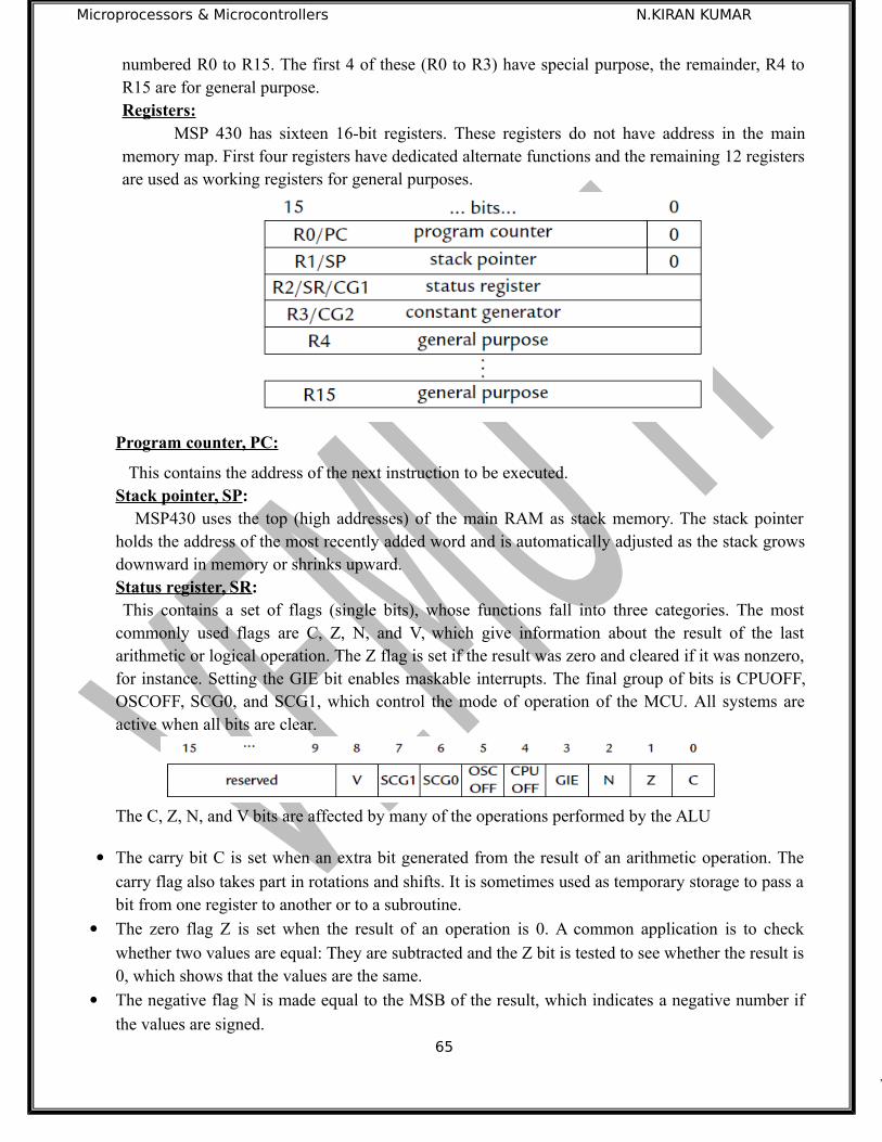
Microprocessors & Microcontrollers N.KIRAN KUMAR
numbered R0 to R15. The first 4 of these (R0 to R3) have special purpose, the remainder, R4 toR15 are for general purpose.Registers:
MSP 430 has sixteen 16-bit registers. These registers do not have address in the mainmemory map. First four registers have dedicated alternate functions and the remaining 12 registersare used as working registers for general purposes.
Program counter, PC:
This contains the address of the next instruction to be executed.Stack pointer, SP:
MSP430 uses the top (high addresses) of the main RAM as stack memory. The stack pointerholds the address of the most recently added word and is automatically adjusted as the stack growsdownward in memory or shrinks upward.Status register, SR: This contains a set of flags (single bits), whose functions fall into three categories. The mostcommonly used flags are C, Z, N, and V, which give information about the result of the lastarithmetic or logical operation. The Z flag is set if the result was zero and cleared if it was nonzero,for instance. Setting the GIE bit enables maskable interrupts. The final group of bits is CPUOFF,OSCOFF, SCG0, and SCG1, which control the mode of operation of the MCU. All systems areactive when all bits are clear.
The C, Z, N, and V bits are affected by many of the operations performed by the ALU
The carry bit C is set when an extra bit generated from the result of an arithmetic operation. The
carry flag also takes part in rotations and shifts. It is sometimes used as temporary storage to pass abit from one register to another or to a subroutine.
The zero flag Z is set when the result of an operation is 0. A common application is to check
whether two values are equal: They are subtracted and the Z bit is tested to see whether the result is0, which shows that the values are the same.
The negative flag N is made equal to the MSB of the result, which indicates a negative number if
the values are signed.65

Microprocessors & Microcontrollers N.KIRAN KUMAR
The signed overflow flag V is set when the result of a signed operation has overflowed, even
though a carry may not be generated.
Enable Interrupts
Setting the general interrupt enable or GIE bit enables maskable interrupts, provided thatthe individual sources of interrupts have themselves been enabled. Clearing the bit disables allmaskable interrupts. There are also non maskable interrupts, which cannot be disabled with GIE.
Control of Low-Power Modes:The CPUOFF, OSCOFF, SCG0, and SCG1 bits control the mode of operation of the MCU.
All systems are fully operational when all bits are clear. Setting combinations of these bits puts thedevice into one of its low-power modes (LPM0 – 4).Constant generator:
This provides the six most frequently used values so that they need not be fetched frommemory whenever they are needed. It uses both R2 and R3 to provide a range of useful values byexploiting the CPU’s addressing modes.General purpose registers: The remaining 12 registers, R4–R15, are general working registers. They may be used for
either data or addresses because both are 16-bit values, which simplify the operation significantly.Emulator:
Emulator, JTAG interface & Spy-Bi wire are used to communicate with desktop computerwhen downloading program and debugging the program. Emulator and simulator is used forchecking the operation of the processor.JTAG:
JTAG Joint Test Action Group is a standardized interface to MSP 430 microcontrollerwith desktop computer that can used for controlling & monitoring during the programmer systemtesting and debugging. JTAG uses 16,24 wires for its operation.Spy-Bi wire:
Spy-Bi wire is used to used to download the software. It requires only two wires. It issimilar to JTAG interface which is also used to communicate MSP430 with desktop computer.
Watchdog timer:Watchdog timer is a safety feature, which resets the processor if any errors or malfunction
occurs in the system. The main purpose of Watchdog timer is to protect the system against failureof the software such as hang or entering into the infinite loop etc. If the selected time intervalexpires, a system reset is generated.
Brown out protection:Brown out protection is used to protect the system if any voltage fluctuations occur in the
system to dangerous level.I/O ports:
I/O ports are used to communicate with the MSP430 by the user or external environment.MSP430 is having no. of GPIO ports and each port size is 8-bit. Each I/O pin is individuallyconfigurable as I/P or O/P pin.
66

Microprocessors & Microcontrollers N.KIRAN KUMAR
A/D converters:Analog signals are converted to digital signals by using ADC. MSP 430 utilizes sigma delta
analog to digital converters to convert analog signal to digital signal.Timers:
Timers are used to generate delays. It can also be used as counters which perform countingoperations. Power supply:
There are GND & VCC connections for power supply. For ground it has 0 V and for VCC itprovides + 5V. MSP 430 is applicable to low power applications it can operate up to 1.8 V to 3.6V.
All the blocks in MSP 430 are connected through Memory address bus (MAB) andMemory data bus (MDB). MAB is unidirectional and MDB is bidirectional.Advantages:
Stack processing capability
RISC architecture
Real time capability with ultra low power consumption
Digitally controlled oscillator controlled
Disadvantages:Number of pins are moreBlock diagram is complexHigh power mode will be operated
MSP 430 FAMILY VARIANTS/ SERIES
Features of Various MSP430 FamiliesMSP430x1xx series
Power specification overview, as low as:
μA RAM retention
0.7 μA real-time-clock mode
200 μA / MIPS active
Features fast wakeup from standby mode in less than 6 μs.
Device parameters
Flash options: 1–60 KB
ROM options: 1–16 KB
RAM options: 128 B–10 KB
GPIO options: 14, 22, 48 pins
67
Microprocessors & Microcontrollers N.KIRAN KUMAR
ADC options: Slope, 10 & 12bitSAR
Other integrated peripherals: 12bit DAC, up to 2 16bit timers, watchdog timer,
brownout reset, SVS, USART module (UART, SPI), DMA, 16×16 multiplier,Comparator A, temperature sensor
Applications: stepper motor controller, wireless mouse, electric meter.
MSP430F2xx seriesPower specification overview, as low as:
μA RAM retention
0.3 μA standby mode (VLO)
0.7 μA real-time-clock mode
220 μA / MIPS active
Feature ultrafast wakeup from standby mode in less than 1 μs
Device parameters
Flash options: 1–120 KB
RAM options: 128 B – 8 KB
GPIO options: 10, 11, 16, 24, 32, and 48 pins
ADC options: Slope, 10 & 12bit SAR, 16 & 24bit Sigma Delta
Other integrated peripherals: operational amplifiers, 12bit DAC, up to 2 16-bit timers,
watchdog timer, brownout reset, SVS, USI module (I²C, SPI), USCI module, DMA,16×16 multiplier, Comparator_A+, temperature sensor
Applications:e-metering
MSP430G2xx seriesUltra Low Power, as low as (@2.2 V):
0.1μA RAM retention
0.4 μA Standby mode (VLO)
0.7 μA real-time-clock mode
220 μA / MIPS active
UltraFast wake-up from Standby Mode in <1 μs
Device parameters
Flash options: 0.5–56 KB
RAM options: 128 B–4 KB
GPIO options: 10, 16, 24, 32 pins
ADC options: Slope, 10bit SAR
Other integrated peripherals: Capacitive Touch I/O, up to 3 16-bit timers, watchdog
timer, brownout reset, USI module (I²C, SPI), USCI module, Comparator_A+, Tempsensor
MSP430x3xx seriesPower specification overview, as low as:
0.1μA RAM retention
68

Microprocessors & Microcontrollers N.KIRAN KUMAR
0.9 μA real-time-clock mode
160 μA / MIPS active
Features fast wakeup from standby mode in less than 6 μs.
Device parameters:
ROM options: 2–32 KB
RAM options: 512 B–1 KB
GPIO options: 14, 40 pins
ADC options: Slope, 14bit SAR
Other integrated peripherals: LCD controller, multiplier
MSP430x4xx seriesPower specification overview, as low as:
0.1μA RAM retention
0.7 μA real-time-clock mode
200 μA / MIPS active
Features fast wakeup from standby mode in less than 6 μs.
Device parameters:
Flash/ROM options: 4 – 120 KB
RAM options: 256 B – 8 KB
GPIO options: 14, 32, 48, 56, 68, 72, 80 pins
ADC options: Slope, 10 & 12bit SAR, 16bit Sigma Delta
Other integrated peripherals: SCAN_IF, ESP430, 12bit DAC, Op Amps, RTC, up to 2
16bit timers, watchdog timer, basic timer, brownout reset, SVS, USART module (UART,SPI), USCI module, LCD Controller, DMA, 16×16 & 32x32 multiplier, Comparator_A,temperature sensor, 8 MIPS CPU Speed
Applications: energy metering, low power applications
MSP430x5xx seriesPower specification overview, as low as:
0.1μA RAM retention
2.5 μA real-time-clock mode
165 μA / MIPS active
Features fast wakeup from standby mode in less than 5 μs.
Device parameters:
Flash options: up to 512 KB
RAM options: up to 66 KB
ADC options: 10 & 12bit SAR
GPIO options: 29, 31, 47, 48, 63, 67, 74, 87 pins
Other integrated peripherals: High resolution PWM, 5 V I/O's, USB, up to 4 16-bit
timers, watchdog timer, Real Time Clock, brownout reset, SVS, USCI module, DMA,32x32 multiplier, Comp B, temperature sensor.
69
Microprocessors & Microcontrollers N.KIRAN KUMAR
Applications: USB, RF connectivity and consumer electronics.
MSP430x6xx seriesPower specification overview, as low as:
0.1μA RAM retention
2.5 μA real-time-clock mode
165 μA / MIPS active
Features fast wakeup from standby mode in less than 5 μs
Device parameters:
Flash options: up to 512 KB
RAM options: up to 66 KB
ADC options: 12bit SAR
GPIO options: 74 pins
Other integrated peripherals: USB, LCD, DAC, Comparator_B, DMA, 32x32 multiplier,
power management module (BOR, SVS, SVM, LDO),watchdog timer, RTC, Tempsensor.
MSP430x5xx Series Block Diagram Unified clock system:
The unified clock system consists of three clock signals namely Master clock, Sub system masterclock and Auxiliary clock.
The master clock is used by the CPU and few peripherals.
SMCLK is distributed to peripherals.
ACLK is also distributed to peripherals.
MCLK & SMCLK run at same frequencies which are at mega hertz range. ACLK isderived from a watch crystal and therefore runs at lower frequency.
Power management module:The power management module is used for supervision of power supply voltages.
DMA (Direct Memory Access):Direct memory access is used when huge amount of data is to be transferred without CPU from
memory to I/O.Watchdog Timer Module:
Watchdog timer is used when fault occurs in the system then watchdog timer resetsautomatically the system. The main purpose of watchdog timer is to protect the system againstfailure of software.Hardware multiplier:
The multiplication operation is supported by a dedicated peripheral module. The moduleperforms operations with 32-, 24-, 16-, and 8-bit operands. The module supports signed andunsigned multiplication as well as signed and unsigned multiply-and-accumulate operations.
70
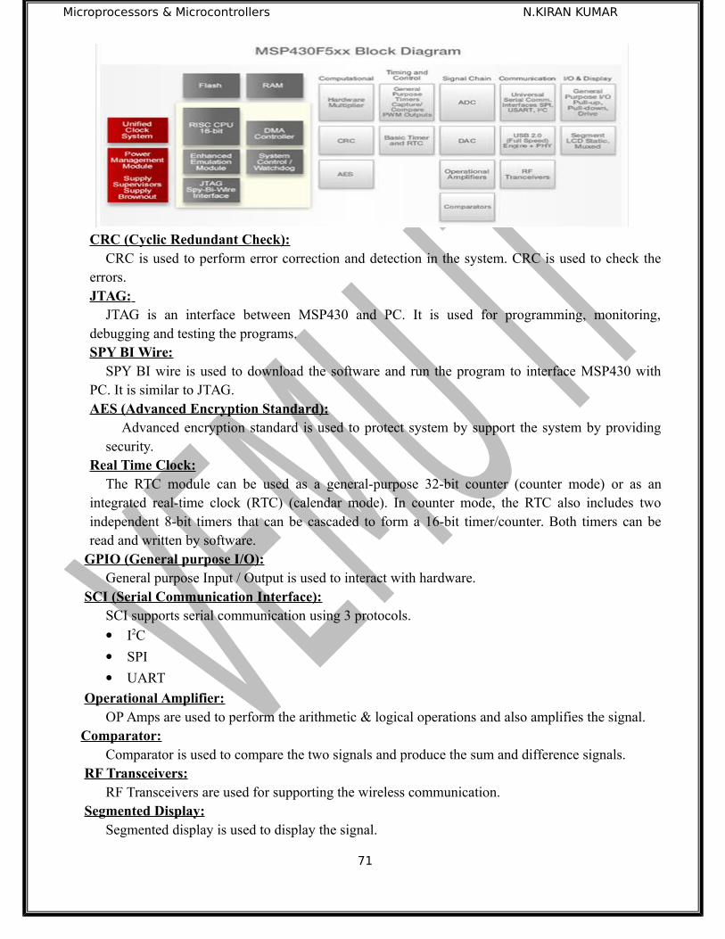
Microprocessors & Microcontrollers N.KIRAN KUMAR
CRC (Cyclic Redundant Check):CRC is used to perform error correction and detection in the system. CRC is used to check the
errors.JTAG:
JTAG is an interface between MSP430 and PC. It is used for programming, monitoring,debugging and testing the programs.SPY BI Wire:
SPY BI wire is used to download the software and run the program to interface MSP430 withPC. It is similar to JTAG.AES (Advanced Encryption Standard):
Advanced encryption standard is used to protect system by support the system by providingsecurity.
Real Time Clock:The RTC module can be used as a general-purpose 32-bit counter (counter mode) or as an
integrated real-time clock (RTC) (calendar mode). In counter mode, the RTC also includes twoindependent 8-bit timers that can be cascaded to form a 16-bit timer/counter. Both timers can beread and written by software.
GPIO (General purpose I/O):General purpose Input / Output is used to interact with hardware.
SCI (Serial Communication Interface):SCI supports serial communication using 3 protocols.
I2C
SPI
UART
Operational Amplifier:OP Amps are used to perform the arithmetic & logical operations and also amplifies the signal.
Comparator:Comparator is used to compare the two signals and produce the sum and difference signals.
RF Transceivers:RF Transceivers are used for supporting the wireless communication.
Segmented Display:Segmented display is used to display the signal.
71

Microprocessors & Microcontrollers N.KIRAN KUMAR
Universal Serial Bus (USB)The features of the USB module include:
• Fully compliant with the USB 2.0 full-speed specification– Full-speed device (12 Mbps) with integrated USB transceiver (PHY)– Supports control, interrupt, and bulk transfers– Supports USB suspend, resume, and remote wakeup
• A power supply system independent from the PMM system– Integrated 3.3-V LDO regulator with sufficient output to power entire MSP430 andsystem circuitry from 5-V VBUS
– Integrated 1.8-V LDO regulator for PHY and PLL– Easily used in either bus-powered or self-powered operation– Current-limiting capability on 3.3-V LDO output
• Internal 48-MHz USB clock– Integrated programmable PLL– Highly-flexible input clock frequencies for use with lowest-cost crystals
• 2KB of dedicated USB buffer space for endpoints• When USB is disabled
– Buffer space is mapped into general RAM, providing additional 2KB to the system– USB interface pins become high-current general purpose I/O pins
I/O Ports and Registers: I/O ports are used to communicate with the MSP430 by the user or external environment.
MSP430 is having no. of GPIO ports (number will vary with family) and each port size is 8-
bit.
Each I/O pin is individually configurable as I/p or o/p pin.
Each I/O pin is having separate pull-up and pull-down resistors, data input and output
registers.
All the I/O pins can be configured as digital I/O pin or module pin.
P1 & P2 ports having interrupt capability.
P1 & P2 interrupts are prioritized with P1.0 is highest and P1.7 is lowest. Similarly for P2
Both P1 & P2 having separate interrupt vector registers P1IV and P2IV respectively.
CPU:CPU has a 16 bit ALU, 4 Special function registers, 12 general function registers The MSP430 CPU includes an arithmetic logic unit (ALU) that handles addition,
subtraction, comparison and logical (AND, OR, XOR) operations ALU operations can affect the overflow, zero, negative, and carry flags in the status register. 12 general purpose registers saves CPU cycles by allowing the storage of frequently used
values and variables instead of using RAM. Registers can hold a word of 16bits
Program counter: The 16-bit Program Counter (PC/R0) points to the next instruction to be read from memory
and executed by the CPU.
72

Microprocessors & Microcontrollers N.KIRAN KUMAR
The Program counter is implemented by the number of bytes used by the instruction (2, 4, or6 bytes, always even).
It is important to note that the PC is aligned at even addresses, because the instructions are 16 bits, even though the individual memory addresses contain 8-bit values.
Stack Pointer: When a subroutine is called the CPU jumps to the subroutine, executes the code then returns
to instruction after the call instruction. It must keep track of the contents of the PC before jumping to the subroutine, so that it can
return afterward. This is the primary purpose of the stack. Some processors use separate hardware for the stack. But MSP430 uses the top of Main RAM. The Stack Pointer (SP/R1) is located in R1. The SP holds the address of most recently added word and is automatically grows downward
in memory. Stack can be used by user to store data for later use(instructions: store by PUSH, retrieve by
POP. Stack can be used by user or by compiler for subroutine parameters (PUSH, POP in calling
routine; addressed via offset calculation on stack pointer (SP) in called subroutine) Stack can be used by subroutine calls to store the program counter value for return at
subroutine's end (RET). Status registers:
The Status Register (SR/R2) is a 16 bit register, and it stores the status and control bits. The system flags are changed automatically by the CPU depending on the result of an operation in a register. The reserved bits of the SR are used to support the constants generator.
73
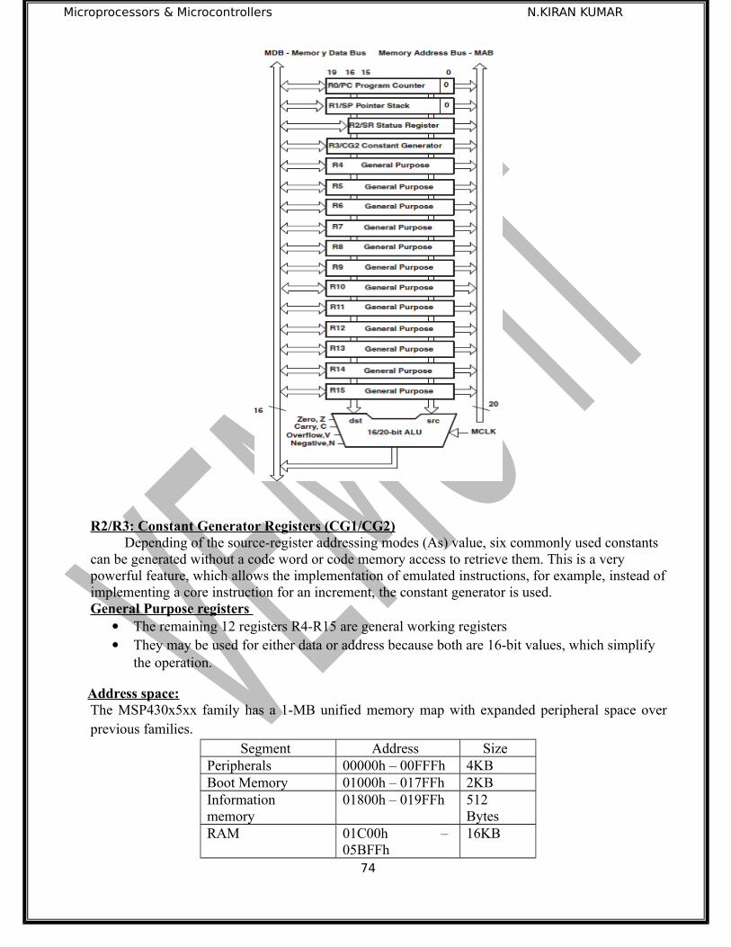
Microprocessors & Microcontrollers N.KIRAN KUMAR
R2/R3: Constant Generator Registers (CG1/CG2) Depending of the source-register addressing modes (As) value, six commonly used constants
can be generated without a code word or code memory access to retrieve them. This is a very powerful feature, which allows the implementation of emulated instructions, for example, instead ofimplementing a core instruction for an increment, the constant generator is used.General Purpose registers
The remaining 12 registers R4-R15 are general working registers They may be used for either data or address because both are 16-bit values, which simplify
the operation.
Address space:The MSP430x5xx family has a 1-MB unified memory map with expanded peripheral space overprevious families.
Segment Address SizePeripherals 00000h – 00FFFh 4KBBoot Memory 01000h – 017FFh 2KBInformationmemory
01800h – 019FFh 512Bytes
RAM 01C00h –05BFFh
16KB
74
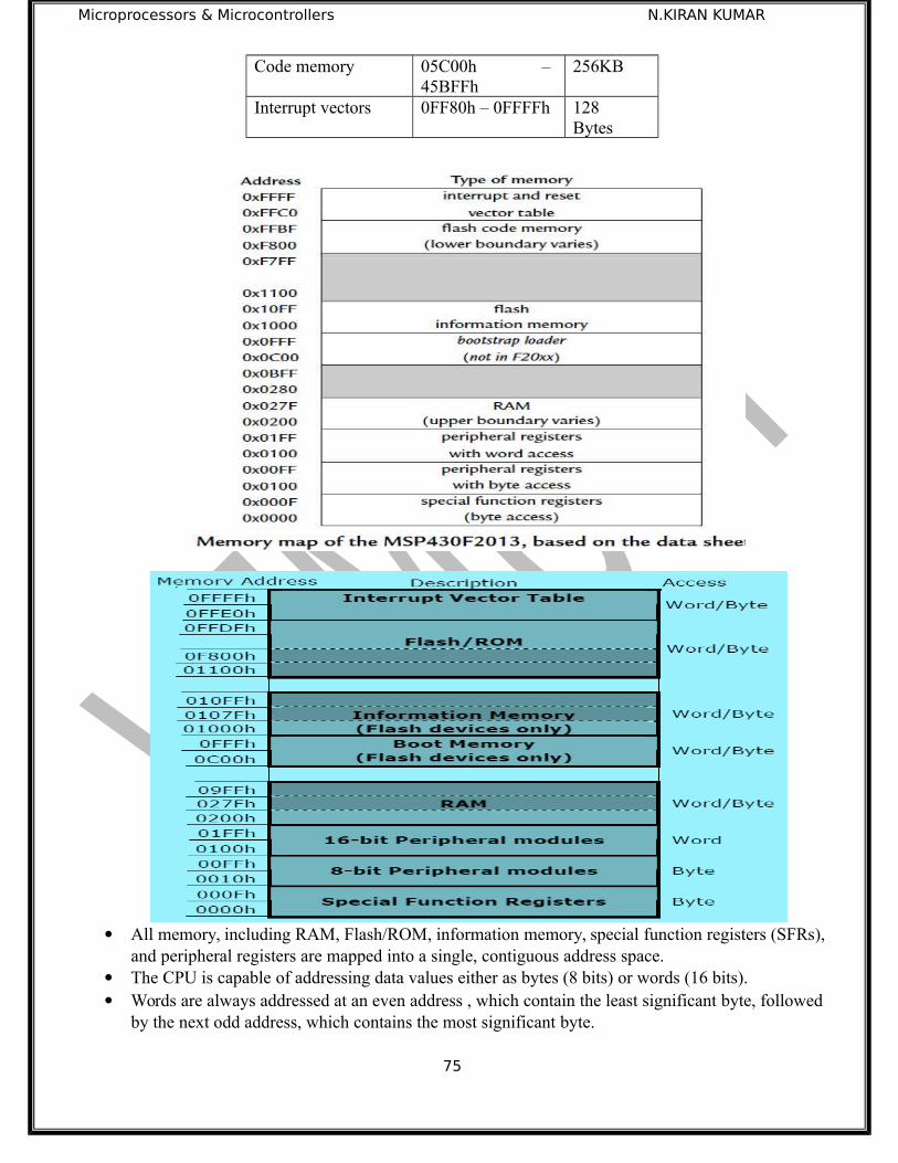
Microprocessors & Microcontrollers N.KIRAN KUMAR
Code memory 05C00h –45BFFh
256KB
Interrupt vectors 0FF80h – 0FFFFh 128Bytes
All memory, including RAM, Flash/ROM, information memory, special function registers (SFRs),and peripheral registers are mapped into a single, contiguous address space.
The CPU is capable of addressing data values either as bytes (8 bits) or words (16 bits). Words are always addressed at an even address , which contain the least significant byte, followed
by the next odd address, which contains the most significant byte.
75

Microprocessors & Microcontrollers N.KIRAN KUMAR
For 8-bit operations, the data can be accessed from either odd or even addresses, but for 16-bit operations, the data values can only be accessed from even addresses
The interrupt vector table is mapped at the very end of memory space (upper 16 words ofFlash/ROM), in locations 0FFE0h through to 0FFFEh. The priority of the interrupt vectorincreases with the word address. It is used to store the addresses of interrupts.
The start address of Flash/ROM depends on the amount of Flash/ROM present on the device.The start address varies between01100h (60k devices) to 0F800h (2k devices) and always runs tothe end of the address space at location 0FFFFh.
Flash can be used for both code and data. Word or byte tables can also be stored and read by theprogram from Flash/ROM. All code, tables, and hard-coded constants reside in this memorySpace.
The MSP430 flash devices contain an address space for information memory. It is like anonboard EEPROM, where variables needed for the next power up can be stored during powerdown. It can also be used as code memory
The MSP430 flash devices contain an address space for boot memory, located between addresses0C00h through to 0FFFh.
The bootstrap loader is located in this memory space, which is an External interface that can beused to program the flash memory in addition to the JTAG.This memory region is not accessibleby other applications, so it cannot be overwritten accidentally.
RAM always starts at address 0200h. The end address of RAM depends on the amount of RAMpresent on the device. RAM is used for both code and data
Peripheral modules consist of all on-chip peripheral registers that are mapped into the addressspace. These modules can be accessed with byte or word instructions, depending if the peripheralmodule is 8-bit or 16-bit respectively.
The 16-bit peripheral modules are located in the address space from addresses 0100 through to01FFh and the 8-bit peripheral modules are mapped into memory from addresses 0010h throughto 00FFh.
The Special Function Registers (SFRs) are located at memory addresses from 0000h to 000Fh.SFRs must be accessed using byte instructions only.
ADDRESSING MODES OF MSP430:
Addressing mode means the way of specifying the operands in an instruction. The MSP430 has
seven addressing modes to interact with the CPU registers. All 16 of these are treated on an almost
equal basis, including the four special-purpose registers R0–R3 or PC, SP, SR/CG1, and CG2.
The MSP430 supports seven addressing modes for the source operand and four addressing
modes for the destination operand. They are
Register mode
Indexed mode
Symbolic mode
Absolute mode
Indirect register mode
76

Microprocessors & Microcontrollers N.KIRAN KUMAR
Indirect auto increment mode
Immediate mode
Register ModeThis uses one or two of the registers in the CPU. It is the most straightforward addressing
mode and is available for both source and destination.
Ex: MOV.W R4, R5 - Move (copy) the contents of source (register R4) to destination (R5).
The registers are specified in the instruction word; no further data are needed. It is also the
fastest mode and this instruction takes only 1 cycle.
Any of the 16 registers can be used for either source or destination but there are some
special cases:
The PC is incremented by 2 while the instruction is being fetched, before it is used as a
source.
The constant generator CG2 reads 0 as a source.
Both PC and SP must be even because they address only words, so the LSB is discarded
if they are used as the destination.
SR can be used as a source and destination in almost the usual way although there are
some details about the behavior of individual bits.
For byte instructions,
Operands are taken from the lower byte; the upper byte is not affected.
The result is written to the lower byte of the register and the upper byte is cleared.
Indexed ModeThe Indexed mode commands are formatted as X(Rn), where X is a constant and Rn is one
of the CPU registers. The absolute memory location is addressed by adding a constant base address
to the contents of a CPU register; the value in the register is not changed.
Ex : MOV.B 3(R5), R4
Move (copy) the contents at source address (3+R5) to destination (register R4)
Indexed addressing can be used for the source, destination, or both. The base addresses, just
the single value 3 here because only one address is indexed, are stored in the words following the
instruction. They cannot be produced by the constant generator.
Symbolic Mode
Symbolic mode allows the assignment of labels to fixed memory locations, so that those
locations can be addressed directly with the assigned label name. For example, suppose that a
77

Microprocessors & Microcontrollers N.KIRAN KUMAR
program uses the variable LoopCtr, which occupies a word. The following instruction stores the
value of LoopCtr in R6 using symbolic mode.
Ex: mov.w LoopCtr ,R6 ; load word LoopCtr into R6
Absolute Mode
It is similar to Symbolic mode, with the difference that the label is preceded by “&”. The
word following the instruction contains the absolute address.
Ex: mov.b &P1IN ,R6 ; load byte P1IN into R6
Where P1IN is the absolute address of the register. This addressing mode is used for special
function and peripheral registers, whose addresses are fixed in the memory map. This addressing
mode can be used for both source and destination operands.
The instruction in above example is written in indexed mode as below:
mov.b P1IN(SR),R6 ; load byte P1IN into R6
Here PIN is already the complete address required so it should be added to a register that
contains 0. The MSP430 mimics this by using the status register SR which provides a constant 0
i.e., it behaves as CG1 when it is used as the base for indexed addressing.
Register indirect mode
This is available only for the source operand and is shown by the symbol @ in front of a
register, @Rn. It means that the contents of Rn are used as the address of the operand. In other
words, Rn holds a pointer rather than a value.
Ex: mov.w @R5 ,R6 ; load word from address (R5)=4 into R6
The address of the source is 4, which is in R5. Thus a word is loaded from address 4 into
R6. The value in R5 is unchanged. This has exactly the same effect as indexed addressing with a
base address of 0 but saves a word of program memory, which also makes it faster.
Indirect addressing cannot be used for the destination so indexed addressing must be used
instead by emulating the instruction as below.
mov.w R6 ,0( R5) ; store word from R6 into address 0+(R5)=4
The penalty is that a word of 0 must be stored in the program memory and fetched from it.
The constant generator cannot be used.
Indirect Autoincrement Mode
This is also applicable only for the source operand and the format is specified with a symbol ‘@’
in front of the register and + sign after it, such as @Rn+. Here, Rn register value is used as data
pointer and increments the register content after the operation by 1 (for byte operations) or 2 (for
word operation).
78

Microprocessors & Microcontrollers N.KIRAN KUMAR
Ex: mov.w @R5+,R6
A word is loaded from address 4 into R6 and the value in R5 is incremented to 6 because a word
(2 bytes) was fetched.
This mode cannot be used for the destination. Instead the main instruction must use indexed
mode with an offset of 0, followed by an explicit increment of the register by 1 or 2. The reverse of
this move therefore needs two instructions:
mov.w R6 ,0( R5) ; store word from R6 into address 0+(R5)=4
incd.w R5 ; R5 += 2
Immediate Mode
In this addressing mode, the immediate data is specified as the operand in the instruction i.e., the
data is readily available as a part instruction that will be fetched from the memory for the
operation.
Immediate mode is used to assign constant values to registers or memory locations. The
immediate data cannot be a destination operand.
Ex: mov.w #0900h,R5
On–chip Peripherals:
FRAM Technology:Ferro electric Random Access Memory is a memory technology that contains the best features of
flash and SRAM. It is a non volatile like flash but it is fast & low power writes.Hardware Multiplier:
79
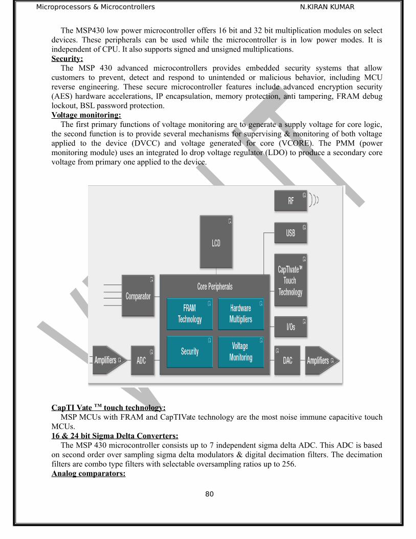
Microprocessors & Microcontrollers N.KIRAN KUMAR
The MSP430 low power microcontroller offers 16 bit and 32 bit multiplication modules on selectdevices. These peripherals can be used while the microcontroller is in low power modes. It isindependent of CPU. It also supports signed and unsigned multiplications.Security:
The MSP 430 advanced microcontrollers provides embedded security systems that allowcustomers to prevent, detect and respond to unintended or malicious behavior, including MCUreverse engineering. These secure microcontroller features include advanced encryption security(AES) hardware accelerations, IP encapsulation, memory protection, anti tampering, FRAM debuglockout, BSL password protection.Voltage monitoring:
The first primary functions of voltage monitoring are to generate a supply voltage for core logic,the second function is to provide several mechanisms for supervising & monitoring of both voltageapplied to the device (DVCC) and voltage generated for core (VCORE). The PMM (powermonitoring module) uses an integrated lo drop voltage regulator (LDO) to produce a secondary corevoltage from primary one applied to the device.
CapTI Vate TM touch technology:MSP MCUs with FRAM and CapTIVate technology are the most noise immune capacitive touch
MCUs.16 & 24 bit Sigma Delta Converters:
The MSP 430 microcontroller consists up to 7 independent sigma delta ADC. This ADC is basedon second order over sampling sigma delta modulators & digital decimation filters. The decimationfilters are combo type filters with selectable oversampling ratios up to 256.Analog comparators:
80

Microprocessors & Microcontrollers N.KIRAN KUMAR
This module supports precision slope ADCs, supply voltage supervision & monitoring of externalanalog signals.Operational amplifiers:
OP amps supports front end analog signal conditioning prior to ADC. OP amp output slew ratecan be configured.LCD drivers:
MSP 430 supports up to 320 segments individual blinking segments control. This controllerincludes a proven core that has been optimized for low power modes.Inputs/Outputs:
MSP 430 is designed to support a variety of need dependent upon specific applications or pinconfigurable settings. I/O pins may e multiplexed with multiple peripherals providing layout andperipheral flexibility.USB:
Development is made easy with USB developer’s package & tools like MSP 430 also uses USBvender.Instruction set:
Generally instruction set is having Op Code Source Operand Destination Operand
Byte, word and address instructions are accessed using the .B, .W or .A extensions. Byteinstructions are used to access byte data or byte peripherals. Word instructions are used to accessword data or word peripherals. If no extension is used, the instruction is a word instruction.
There are two types of instructions. They are Core instructions Emulated instructions
Core instructions that have unique op-codes are decoded by CPU. The Emulated instructionsare instructions that make code easier to write and read data but don’t have op-codes themselvesinstead they are replaced automatically by the assembler with an equivalent core instruction.
There are three core-instruction formats: Double-operand Single-operand Program flow control
Movement instructions:There is only the one ‘mov’ instruction to move data. It can address all of memory as either sourceor destination, including both registers in the CPU and the whole memory map.
mov . w src , dstHere w denotes that the operations can use either bytes or wordsStack Operations:
Stack operations are used to transfer data to stack. The data can be inserted into stack byperforming PUSH operation and the data can be deleted from stack by performing POP operation.
push .w src ; push data onto stack pop .w dst ; pop data off stack.
Arithmetic instructions with two operands:
operationoperands action
81

Microprocessors & Microcontrollers N.KIRAN KUMAR
add .w src , dst add
dst + = src
addc .w src , dst add with carry dst += ( src + C)
adc .w dst add carry bit dst + = C
sub .w src , dst subtract dst - = scr
subc .w src , dst subtract with borrow dst - = (scr+~C)
sbc .w dst Subtract borrow bit dst - = ~C -Emulated
cmp .w src , dst compare , set flags only (dst – scr)
Arithmetic instructions with one operand: All these instructions are emulated, which means the operands is always in destination.
operation operands action
clr .w dst clear dst = 0
dec .w dst decrement dst - -
decd .w dst double decrement dst- = 2
inc .w dst increment dst ++
incd .w dst double increment dst+ = 2 tst .w dst test ( compare with 0) ( dst – 0)
Decimal arithmetic instructions:Decimal arithmetic instructions are used when BCD values are operands.
operation operands action
dadd .w src , dst Decimal add with carry dst+ = src +c
dadc .w dst Decimal add carry bit dst+ =c
Logical instructions with two operands:
operation operands action
and .w src , dst Bitwise AND dst&=scr
xor .w src ,dst Bitwise XOR dst^=scr
bit .w src , dst Bitwise test set flag only
(dst&scr)
bis .w Src, dst Bit set dst|=scr bic .w src , dst Bit clear dst&=~scr
Logical instructions with one operand:
82
Microprocessors & Microcontrollers N.KIRAN KUMAR
There is only one instruction of this type. invert ‘inv’ instruction , also known as onescomplement ,which changes all 0 bits to 1 and 1s to 0
inv.w dst ; invert bitsByte Manipulation:These instructions do not need a suffix because the size of. the operands is fixed. Swpb src
; swap upper and lower bytes (word only)
Sxt src ; extend sign of lower byte (word only)
Operations on bits in status register
operation action
clrc Clear carry bit C=0 clrn Clear negative bit N=0 clrz Clear zero bit Z=0 setc Set carry bit C=1 setn Set negative bit N=1 setz Set zero bit Z=1 dint Disable general interrupts GIE=0
eint Enable general interrupts GIE=1
Shift and rotate instructions:There are three types of shifts
Logical shift: Inserts zeroes for both right and left shifts. arithmetic shift: Inserts zeroes for left shifts but the most significant bit, which carries the
sign, is replicated for right shiftsEx : rla dst ; arithmetic shift left rra src ; arithmetic shift right.
Rotation: Does not introduce or lose any bits; bits are moved out of one end of the registerare passed around to the other.Ex: rlc dst ; rotate left through carry. rrc src ; rotate right through carry
83
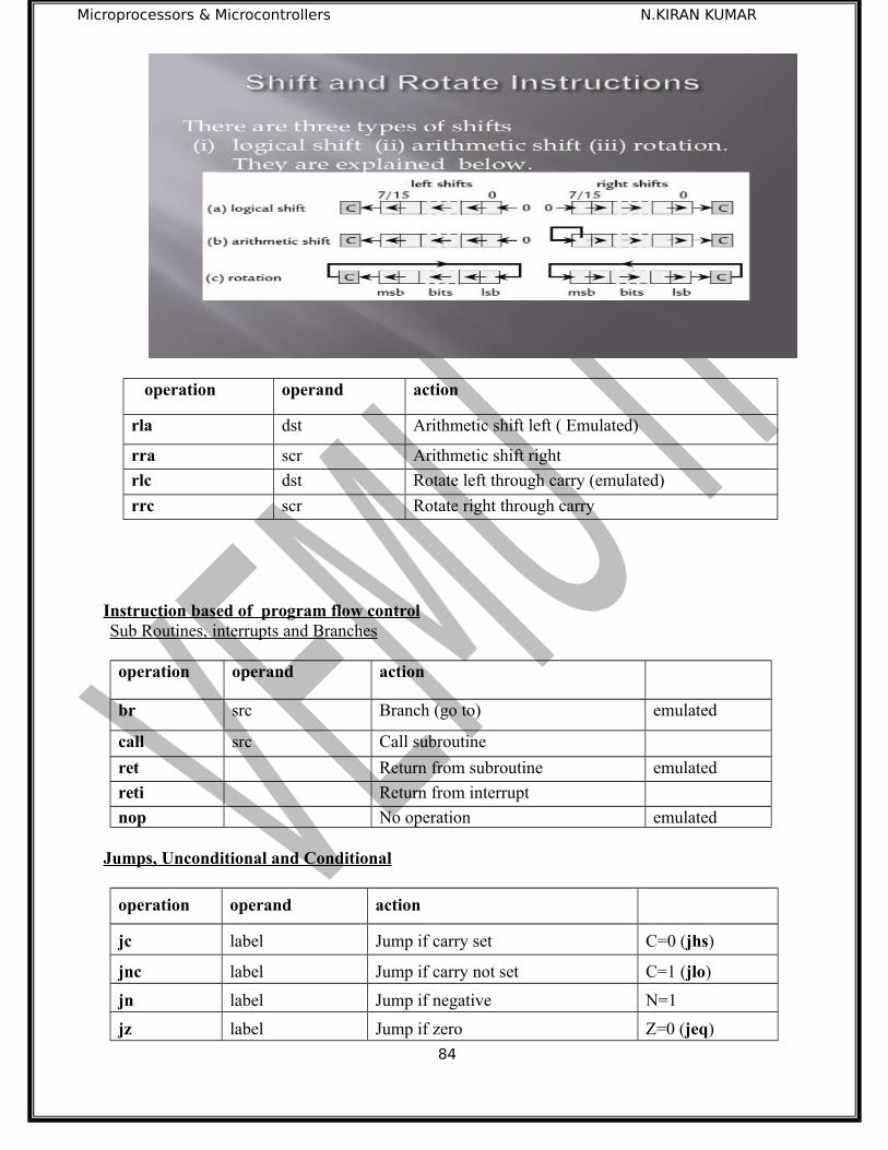
Microprocessors & Microcontrollers N.KIRAN KUMAR
operation operand action
rla dst Arithmetic shift left ( Emulated)
rra scr Arithmetic shift right
rlc dst Rotate left through carry (emulated)
rrc scr Rotate right through carry
Instruction based of program flow controlSub Routines, interrupts and Branches
operation operand action
br src Branch (go to) emulated
call src Call subroutine
ret Return from subroutine emulated
reti Return from interrupt
nop No operation emulated
Jumps, Unconditional and Conditional
operation operand action
jc label Jump if carry set C=0 (jhs)
jnc label Jump if carry not set C=1 (jlo)
jn label Jump if negative N=1
jz label Jump if zero Z=0 (jeq)
84
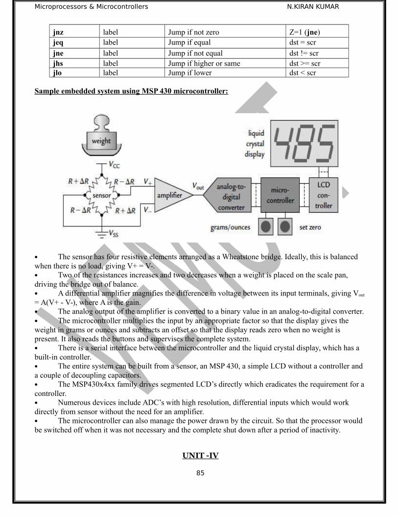
Microprocessors & Microcontrollers N.KIRAN KUMAR
jnz label Jump if not zero Z=1 (jne) jeq label Jump if equal dst = scr
jne label Jump if not equal dst != scr jhs label Jump if higher or same dst >= scr jlo label Jump if lower dst < scr
Sample embedded system using MSP 430 microcontroller:
The sensor has four resistive elements arranged as a Wheatstone bridge. Ideally, this is balanced when there is no load, giving V+ = V-. Two of the resistances increases and two decreases when a weight is placed on the scale pan, driving the bridge out of balance. A differential amplifier magnifies the difference in voltage between its input terminals, giving Vout
= A(V+ - V-), where A is the gain. The analog output of the amplifier is converted to a binary value in an analog-to-digital converter. The microcontroller multiplies the input by an appropriate factor so that the display gives the weight in grams or ounces and subtracts an offset so that the display reads zero when no weight is present. It also reads the buttons and supervises the complete system. There is a serial interface between the microcontroller and the liquid crystal display, which has a built-in controller. The entire system can be built from a sensor, an MSP 430, a simple LCD without a controller and a couple of decoupling capacitors. The MSP430x4xx family drives segmented LCD’s directly which eradicates the requirement for acontroller. Numerous devices include ADC’s with high resolution, differential inputs which would work directly from sensor without the need for an amplifier. The microcontroller can also manage the power drawn by the circuit. So that the processor would be switched off when it was not necessary and the complete shut down after a period of inactivity.
UNIT -IV
85
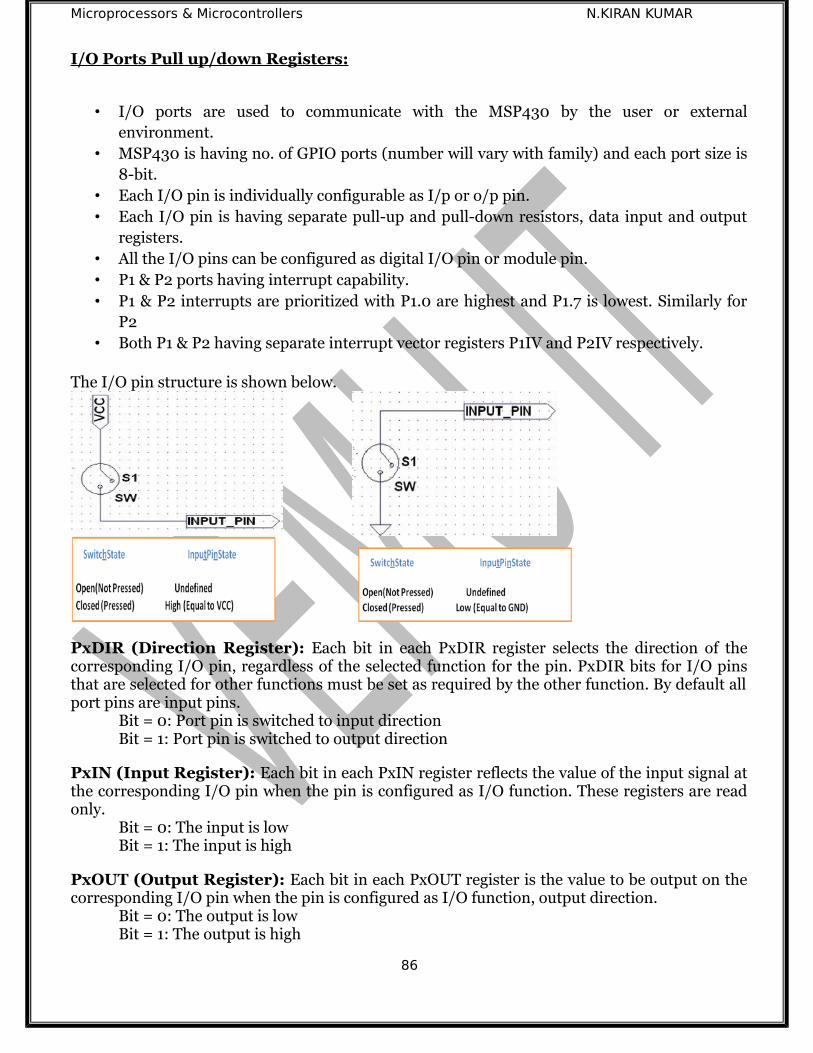
Microprocessors & Microcontrollers N.KIRAN KUMAR
I/O Ports Pull up/down Registers:
• I/O ports are used to communicate with the MSP430 by the user or externalenvironment.
• MSP430 is having no. of GPIO ports (number will vary with family) and each port size is8-bit.
• Each I/O pin is individually configurable as I/p or o/p pin.• Each I/O pin is having separate pull-up and pull-down resistors, data input and output
registers.• All the I/O pins can be configured as digital I/O pin or module pin.• P1 & P2 ports having interrupt capability.• P1 & P2 interrupts are prioritized with P1.0 are highest and P1.7 is lowest. Similarly for
P2• Both P1 & P2 having separate interrupt vector registers P1IV and P2IV respectively.
The I/O pin structure is shown below.
PxDIR (Direction Register): Each bit in each PxDIR register selects the direction of thecorresponding I/O pin, regardless of the selected function for the pin. PxDIR bits for I/O pinsthat are selected for other functions must be set as required by the other function. By default allport pins are input pins.
Bit = 0: Port pin is switched to input directionBit = 1: Port pin is switched to output direction
PxIN (Input Register): Each bit in each PxIN register reflects the value of the input signal atthe corresponding I/O pin when the pin is configured as I/O function. These registers are readonly.
Bit = 0: The input is lowBit = 1: The input is high
PxOUT (Output Register): Each bit in each PxOUT register is the value to be output on thecorresponding I/O pin when the pin is configured as I/O function, output direction.
Bit = 0: The output is lowBit = 1: The output is high
86
Microprocessors & Microcontrollers N.KIRAN KUMAR
If the pin is configured as I/O function, input direction and the pullup/pulldown resistor isenabled, the corresponding bit in the PxOUT register selects pullup or pulldown.
Bit = 0: The pin is pulled downBit = 1: The pin is pulled up
PxREN (Resistor Enable Register): Each bit in each PxREN register enables or disables thepullup/pulldown resistor of the corresponding I/O pin. The corresponding bit in the PxOUTregister selects if the pin is pulled up or pulled down.
Bit = 0: Pullup/pulldown resistor disabledBit = 1: Pullup/pulldown resistor enabled
PxSEL (Selection Register): Port pins are often multiplexed with other peripheral modulefunctions. Each PxSELx bit is used to select the pin function - I/O port or peripheral modulefunction.
Bit = 0: I/O Function is selected for the pinBit = 1: Peripheral module function is selected for the pin
Setting PxSELx = 1 does not automatically set the pin direction. Other peripheral modulefunctions may require the PxDIRx bits to be configured according to the direction needed forthe module function.
PxIE (Interrupt Enable): This read-write register enables interrupts on individual pins.Interrupts on the pins are enabled when their corresponding bits in this register are set. Thisregister is cleared on reset. By default, interrupts are disabled on the port pins.
PxIES (Interrupt Edge Select): This read-write register selects the transition on which aninterrupt occurs. If set, interrupt occurs on a high-to-low transition on the corresponding pin. Ifcleared, an interrupt occurs on a low-to-high transition on the corresponding pin.
PxIFG (Interrupt Flag): Whenever interrupt occurs on the pin then corresponding bitposition is set to ‘1’. This register is cleared by the software before executing RETI instruction inthe ISR.
Bit = 0: No interrupt is pendingBit = 1: An interrupt is pending
Interrupts:
An interrupt is breaking normal program execution. When ever an interrupt occursprocessor runs ISR program. Interrupt can be enabled or disabled. Interrupts can occurred canbe unpredictable when and where it occurs. Interrupts can occur globally, individually orthrough NMI.
Interrupts are commonly used for a range of applications: Urgent tasks that must be executed promptly at higher priority than the main code.
However, it is even faster to execute a task directly by hardware if this is possible. Infrequent tasks, such as handling slow i/o devices. This saves the overhead of regular
polling. Waking the CPU from sleep. This is particularly important in the MSP430, which
typically spends much of its time in a low-power mode and can be awakened only by aninterrupt.
87

Microprocessors & Microcontrollers N.KIRAN KUMAR
The code to handle an interrupt is called an interrupt service routine (ISR). It lookssuperficially like a function but there are a few crucial modifications. The feature that interruptsarise at unpredictable times means that an ISR must carry out its action and clean upthoroughly so that the main code can be resumed without error—it should not be able to tell thatan interrupt occurred.
Each interrupt has a flag, which is raised (set) when the condition for the interruptoccurs.
The MSP430 uses vectored interrupts, which means that the address of each ISR—itsvector—is stored in a vector table at a defined address in memory. In most cases each vector isassociated with a unique interrupt but some sources share a vector.
Each interrupt vector has a distinct priority, which is used to select which vector is takenif more than one interrupt is active when the vector is fetched. The priorities are fixed inhardware and cannot be changed by the user. They are given simply by the address of the vector:A higher address means a higher priority. The reset vector has address 0xFFFE, which gives itthe top priority, followed by 0xFFFC for the single nonmaskable interrupt vector. The vectorsfor the maskable interrupts depend on the peripherals in a particular device and are listed in atable of Interrupt Vector Addresses.
Types of interruptsThe MSP430 offers various interrupt sources, both internal and external. There are three
types of interrupts: Reset
Non-maskable interrupts (NMI)
Maskable interrupts by GIE.
Each one of these interrupts has a priority, determining which interrupt is taken whenmore than one interrupt is pending at any one time. The main difference between non-maskableinterrupts and maskable interrupts is the fact that the non-maskable interrupt (NMI) cannot bedisabled by the General Interrupt Enable (GIE) bit in the Status Register (SR). NMIs are usedfor high priority events such as emergency shutdown of a machine.
Most interrupts are maskable, which means that they are effective only if the generalinterrupt enable (GIE) bit is set in the status register (SR). They are ignored if GIE is clear.Therefore both the enable bit in the module and GIE must be set for interrupts to be generated.
Reset:A reset is a sequence of operations that puts the device into a well-defined state, from
which the user’s program may start. This is obviously necessary when power is first applied. Areset is also generated if the device detects a serious fault in hardware or software from whichthe user’s program cannot be expected to recover. A peculiarity of the MSP430 is that it has twolevels of reset, depending on whether the reset was caused by hardware or software.
Power-on Reset (POR)This is generated by the following severe conditions related to hardware:
The device is powered up. More generally, a POR is raised if the supply voltage drops toso low a value that the device may not work correctly: a brownout.
88
Microprocessors & Microcontrollers N.KIRAN KUMAR
A low external signal on the RST/NMI pin resets the device if the pin is configured for thereset function rather than the non-maskable interrupt. The reset function RST is activeby default.
Larger variants have a more comprehensive supply voltage supervisor (SVS). This isconfigurable, unlike the brownout detector. It sets the SVSFG flag if the voltage fallsbelow the programmed level and can optionally reset the device.
Power-up Clear (PUC)This always follows a power-on reset. It is also generated when software appears to be
out of control in the following ways: The watchdog timer overflows in watchdog mode. The watchdog is active by default and
must either be disabled or regularly cleared before it rolls over. An attempt is made to write to the watchdog control register WDTCTL without the
correct password 0x5A (available as the symbol WDTPW) in the upper byte. A reset istriggered even if the watchdog is disabled or in interval timer mode.
The registers for the flash memory controller, FCTLn, are protected by a password in thesame way as WDTCTL. The value is 0xA5, available as the constant FWKEY. This is toprotect runaway software from corrupting the stored program.
In newer devices, a PUC is triggered by an attempt to fetch an instruction from the rangeof addresses reserved for peripheral registers or to read unimplemented memory.
Non-maskable interrupts (NMI)A non-maskable interrupt can be generated by following sources:
An edge on the RST/NMI pin when configured in NMI mode
An oscillator fault occurs
An access violation to the flash memory
Maskable InterruptsMaskable interrupts are caused by peripherals with interrupt capability. Each maskable
interrupt source can be disabled individually by an interrupt enable bit, or all maskableinterrupts can be disabled by the general interrupt enable (GIE) bit in the status register (SR).
Interrupt Processing:
When an interrupt is requested from a peripheral and the peripheral interrupt enable bitand GIE bit are set, the interrupt service routine is requested. Only the individual enable bitmust be set for non-maskable interrupts to be requested.
Interrupt Acceptance:1. Any currently executing instruction is completed if the CPU was active when the
interrupt was requested. MCLK is started if the CPU was off.2. The PC, which points to the next instruction, is pushed onto the stack.3. The SR is pushed onto the stack.4. The interrupt with the highest priority is selected if multiple interrupts occurred during
the last instruction and are pending for service.
89

Microprocessors & Microcontrollers N.KIRAN KUMAR
5. The interrupt request flag resets automatically on single-source flags. Multiple sourceflags remain set for servicing by software.
6. The SR is cleared. This terminates any low-power mode. Because the GIE bit is cleared,further interrupts are disabled.
7. The content of the interrupt vector is loaded into the PC: the program continues with theinterrupt service routine at that address.
The time taken to start the execution of ISR after an interrupt request is called ‘interruptlatency’. MSP430 takes six clock cycles before the ISR commences. The stack at this point isshown in Figure.
Return from Interrupt:An interrupt service routine must always finish with the special return from interrupt
instruction reti, which has the following actions:1. The SR pops from the stack. All previous settings of GIE and the mode control bits are
now in effect, regardless of the settings used during the interrupt service routine. Inparticular, this re-enables maskable interrupts and restores the previous low-powermode of operation if there was one.
2. The PC pops from the stack and execution resumes at the point where it was interrupted.Alternatively, the CPU stops and the device reverts to its low-power mode before theinterrupt.
This takes a further five cycles in the MSP430. The stack is restored to its state before theinterrupt was accepted.
Interrupt NestingInterrupt nesting is enabled if the GIE bit is set inside an interrupt service routine. When
interrupt nesting is enabled, any interrupt occurring during an interrupt service routine willinterrupt the routine, regardless of the interrupt priorities.
WATCHDOG TIMER:The main purpose of Watchdog timer is to protect the system against failure of the
software such as hang or entering into the infinite loop etc. If the selected time interval expires,a system reset is generated. If the watchdog function is not needed in an application, the modulecan be configured as an interval timer and can generate interrupts at selected time intervals.
Features : Four software selectable time intervals
Watchdog timer mode
Interval timer mode
Access to WDT control register is password protected
Selectable clock source
Can be stopped to conserve power
Clock-fail safe feature
Watchdog timer control register
90

Microprocessors & Microcontrollers N.KIRAN KUMAR
The operation of watchdog timer is controlled by 16-bit register, WDTCTL.
The upper byte is having a password to protect from unexpected write into controlregister. For write operation, WDTCTL password is 5Ah and read operation returns 69h into the
upper byte. The lower byte of WDTCTL contains control bits to configure the timer.
WDTHOLD: This bit stops the operation of the watchdog counter. The clock multiplexer isdisabled and the counter stops incrementing. It holds the last value until the hold bit is resetand the operation continues. It is cleared by the PUC signal.
0: The WDT is fully active.1: The counter is stopped.
WDTNMIES: Watchdog timer NMI edge select. This bit selects the interrupt edge for the NMIinterrupt when WDTNMI =1. Modifying this bit can trigger an NMI.
0: NMI on rising edge1: NMI on falling edge
WDTNMI: Watchdog timer NMI select. This bit selects the function for the RST/NMI pin.0: Reset function1: NMI function
WDTTMSEL: Watchdog timer mode select0: Watchdog mode1: Interval timer mode
WDTCNTCL: Watchdog timer counter clear. Setting WDTCNTCL = 1 clears the count value to0000h. WDTCNTCL is automatically reset.
0: No action1: WDTCNT = 0000h
WDTSSEL: Watchdog timer clock source select0: SMCLK1: ACLK
WDTISx: Watchdog timer interval select. These bits select the watchdog timer interval to setthe WDTIFG flag and/or generate a PUC.
00 Watchdog clock source /3276801 Watchdog clock source /819210 Watchdog clock source /51211 Watchdog clock source /64
The WDT block diagram is shown in below figure
91
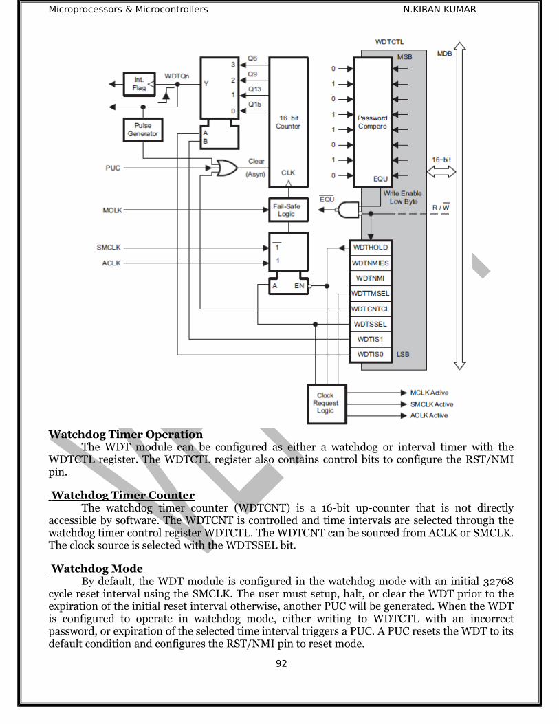
Microprocessors & Microcontrollers N.KIRAN KUMAR
Watchdog Timer OperationThe WDT module can be configured as either a watchdog or interval timer with the
WDTCTL register. The WDTCTL register also contains control bits to configure the RST/NMIpin.
Watchdog Timer CounterThe watchdog timer counter (WDTCNT) is a 16-bit up-counter that is not directly
accessible by software. The WDTCNT is controlled and time intervals are selected through thewatchdog timer control register WDTCTL. The WDTCNT can be sourced from ACLK or SMCLK.The clock source is selected with the WDTSSEL bit.
Watchdog ModeBy default, the WDT module is configured in the watchdog mode with an initial 32768
cycle reset interval using the SMCLK. The user must setup, halt, or clear the WDT prior to theexpiration of the initial reset interval otherwise, another PUC will be generated. When the WDTis configured to operate in watchdog mode, either writing to WDTCTL with an incorrectpassword, or expiration of the selected time interval triggers a PUC. A PUC resets the WDT to itsdefault condition and configures the RST/NMI pin to reset mode.
92

Microprocessors & Microcontrollers N.KIRAN KUMAR
Interval Timer ModeSetting the WDTTMSEL bit to 1 selects the interval timer mode. This mode can be used to
provide periodic interrupts. In interval timer mode, the WDTIFG flag is set at the expiration ofthe selected time interval. A PUC is not generated in interval timer mode at expiration of theselected timer interval and the WDTIFG enable bit WDTIE remains unchanged.
When the WDTIE bit and the GIE bit are set, the WDTIFG flag requests an interrupt. TheWDTIFG interrupt flag is automatically reset when its interrupt request is serviced, or may bereset by software. The interrupt vector address in interval timer mode is different from that inwatchdog mode.
Watchdog Timer InterruptsThe WDT uses two bits in the SFRs for interrupt control.
The WDT interrupt flag, WDTIFG, located in IFG1.0
The WDT interrupt enable, WDTIE, located in IE1.0Watchdog mode: The WDTIFG flag sources a reset vector interrupt. If WDTIFG=1, the WDTinitiates the reset condition, either by timing out or by a password violation. The user hascontrol of the reset source.Interval mode: The WDTIFG flag is set after the selected time interval and requests a WDTinterval timer interrupt if the WDTIE and the GIE bits are set. When the interrupt is serviced,theWDTIFG flag is reset automatically. It also can be reset using software.
Watchdog Timer Clock Fail-Safe OperationThis includes fail-safe logic to preserve the watchdog’s clock. For example, if ACLK is the
WDT clock source, it does not let the device enter LPM4 because that would disable its clock.Therefore it is not possible to use LPM4 with WDT active; the watchdog must first be stopped bysetting WDTHOLD. Similarly, it is not possible to use LPM3 if WDT is active and gets its clockfrom SMCLK. If its clock fails, WDT switches from ACLK or SMCLK to MCLK and takes thisfrom the DCO if an external crystal fails. This feature is not available when WDT is in intervaltimer mode.
SYSTEM CLOCKS:The MSP430 devices have a clock system that allows the CPU and the peripherals to
operate from different clock sources. System clock have conflicting requirements due to following reasons:
Low power Fast start/stop Accurate High performance
Devices often run in low power modes until some event occurs, then system must wakeup andhandles events rapidly. Two kinds of clocks are needed:
Fast clock: Start/ Stop rapidly; clock need not be accurate Slow clock: Runs continuously to monitor real time; uses less power to be accurate
The simplified block diagram of clock system is shown below:
93
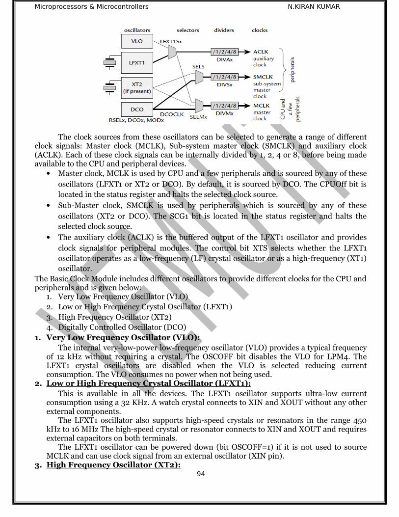
Microprocessors & Microcontrollers N.KIRAN KUMAR
The clock sources from these oscillators can be selected to generate a range of differentclock signals: Master clock (MCLK), Sub-system master clock (SMCLK) and auxiliary clock(ACLK). Each of these clock signals can be internally divided by 1, 2, 4 or 8, before being madeavailable to the CPU and peripheral devices.
Master clock, MCLK is used by CPU and a few peripherals and is sourced by any of theseoscillators (LFXT1 or XT2 or DCO). By default, it is sourced by DCO. The CPUOff bit islocated in the status register and halts the selected clock source.
Sub-Master clock, SMCLK is used by peripherals which is sourced by any of theseoscillators (XT2 or DCO). The SCG1 bit is located in the status register and halts theselected clock source.
The auxiliary clock (ACLK) is the buffered output of the LFXT1 oscillator and providesclock signals for peripheral modules. The control bit XTS selects whether the LFXT1oscillator operates as a low-frequency (LF) crystal oscillator or as a high-frequency (XT1)oscillator.
The Basic Clock Module includes different oscillators to provide different clocks for the CPU andperipherals and is given below:
1. Very Low Frequency Oscillator (VLO)2. Low or High Frequency Crystal Oscillator (LFXT1)3. High Frequency Oscillator (XT2)4. Digitally Controlled Oscillator (DCO)
1. Very Low Frequency Oscillator (VLO):The internal very-low-power low-frequency oscillator (VLO) provides a typical frequency
of 12 kHz without requiring a crystal. The OSCOFF bit disables the VLO for LPM4. TheLFXT1 crystal oscillators are disabled when the VLO is selected reducing currentconsumption. The VLO consumes no power when not being used.
2. Low or High Frequency Crystal Oscillator (LFXT1):This is available in all the devices. The LFXT1 oscillator supports ultra-low current
consumption using a 32 KHz. A watch crystal connects to XIN and XOUT without any otherexternal components.
The LFXT1 oscillator also supports high-speed crystals or resonators in the range 450kHz to 16 MHz The high-speed crystal or resonator connects to XIN and XOUT and requiresexternal capacitors on both terminals.
The LFXT1 oscillator can be powered down (bit OSCOFF=1) if it is not used to sourceMCLK and can use clock signal from an external oscillator (XIN pin).
3. High Frequency Oscillator (XT2):94
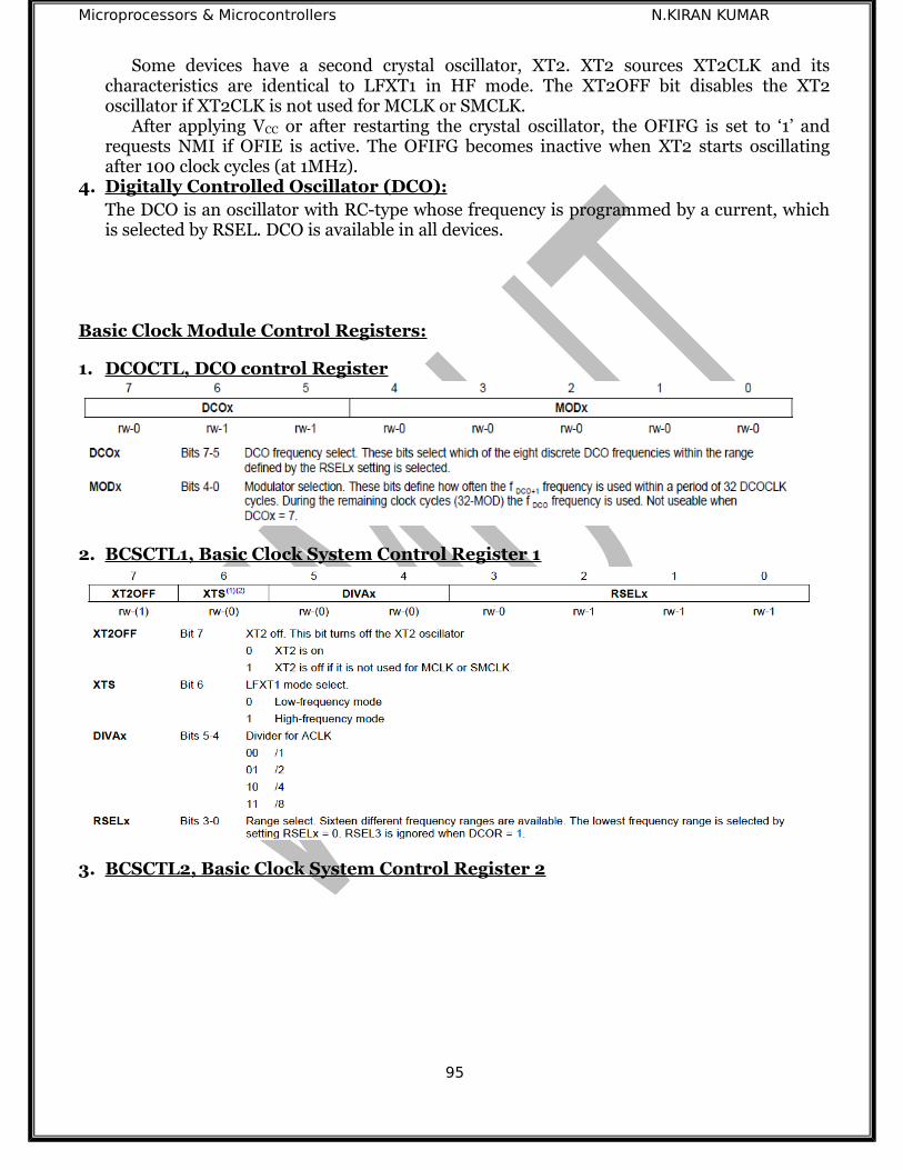
Microprocessors & Microcontrollers N.KIRAN KUMAR
Some devices have a second crystal oscillator, XT2. XT2 sources XT2CLK and itscharacteristics are identical to LFXT1 in HF mode. The XT2OFF bit disables the XT2oscillator if XT2CLK is not used for MCLK or SMCLK.
After applying VCC or after restarting the crystal oscillator, the OFIFG is set to ‘1’ andrequests NMI if OFIE is active. The OFIFG becomes inactive when XT2 starts oscillatingafter 100 clock cycles (at 1MHz).
4. Digitally Controlled Oscillator (DCO):The DCO is an oscillator with RC-type whose frequency is programmed by a current, whichis selected by RSEL. DCO is available in all devices.
Basic Clock Module Control Registers:
1. DCOCTL, DCO control Register
2. BCSCTL1, Basic Clock System Control Register 1
3. BCSCTL2, Basic Clock System Control Register 2
95
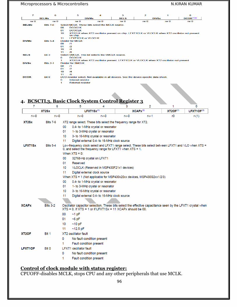
Microprocessors & Microcontrollers N.KIRAN KUMAR
4. BCSCTL3, Basic Clock System Control Register 3
Control of clock module with status register:CPUOFF-disables MCLK, stops CPU and any other peripherals that use MCLK.
96

Microprocessors & Microcontrollers N.KIRAN KUMAR
SCG0-disables SMCLK and stops other peripherals that use SMCLK.SCG1-diasbles DC generator for DCO.OSCOFF-disables VLO & LFXT1MSP430 Low Power Modes
The MSP430 is designed from the ground up for low power. This includes both designand process implementation. Despite this, the bulk of power savings is realized by placing theMSP430 in various power saving modes. We first have to understand what consumes the mostcurrent in the MSP430. This breaks down as follows:
MSP430 CPU draws the most, proportional to the frequency at which it is running.
Clocks and Oscillators, especially high speed clocks.
Modules and PeripheralsSaving power comes down to shutting off as many modules, peripherals, and clocks as we
can, for as long as possible without violating the application time requirements. It is alsoimportant to reduce the speed of the CPU as it can significantly affect power consumption. Thetrade-off is that processing will take longer.
MSP430 peripherals are also designed for low power. For example, the ADC will shut offautomatically after the conversions are finished. The issue is always what to turn off and when,also when to wake them up. Interrupts play a central role because they enable the MSP430 to goto a deep sleep and wake up if events have occurred, either external as detected by GPIOs orinternally generated by the peripherals.
There are four bits that control the CPU and modes of operation present in SR: CPUOff,OscOff, SCG0 and SCG1. The major advantage of including the operating mode bits in the statusregister is that the present state of the operating condition is saved onto the stack during aninterrupt service request. As long as the stored status register information is not altered, theprocessor continues (after RETI) with the same operating mode as before the interrupt event.
These LPM modes refer to the individual bits in the Status Register. By setting andclearing the bits in the SR, one can turn off CPU and clocks resulting in certain Low Power
Modes.
Entering into Low Power modes:To enter into lo power mode the bis (bit set) instruction is used.
bis.w, # LPM3, SR; enters into low power mode 3Exiting from Low Power Modes:To exit from low power mode bic instruction is used.Bic.w, # GIE ! LPM3, SR; enter into normal modeInterrupt to the system can also wakeup MSP 430 from low power mode.Active Vs Standby current consumption:
97

Microprocessors & Microcontrollers N.KIRAN KUMAR
Power consumption depends on clock frequency, ambient temperature, supply voltage, peripheral selection, input/output usage and memory type.
The power consumption profile of the various LPMs:
At 1MHz, we go from 300uA down to less than 1uA by switching to LPM3. This is whatmakes the MSP430 such a good microcontroller for low power applications. It can survive foryears on batteries. But, to take advantage of this, we have to build an application that takesadvantage of these low power modes and turns on only what’s necessary when it’s necessary.
Low power operating modes program flow steps:1) Enable/disable CPUOFF, OSCOFF, SCG0, SCG1 bits in Status register.2) LPM (low power mode) is active after writing to Status register.3) CPU will suspend program execution.4) Disables peripherals
Operating with any disabled clock Individual control register setting
5) All I/O port pins and RAM/Registers are unchanged6) Wakeup is possible through enabled interrupts7) Enter into ISR
Operating mode is saved on stack PC and SR is stored on stack Interrupt vector is moved to PC CPUOFF, OSCOFF, SCG0, SCG1 bits are reset
8) Return from ISR Status register is popped from stack Restore previous mode
9) Interrupt wakes up MSP 430
FRAM Vs Flash for low power & reliabilityFerroelectric Random Access Memory (FRAM) is an ultra-low power nonvolatile memory
technology with write speeds similar to static RAM (SRAM). The technology has been in theindustry for over a decade, implemented as stand-alone memory. FRAM's first introduction as
98
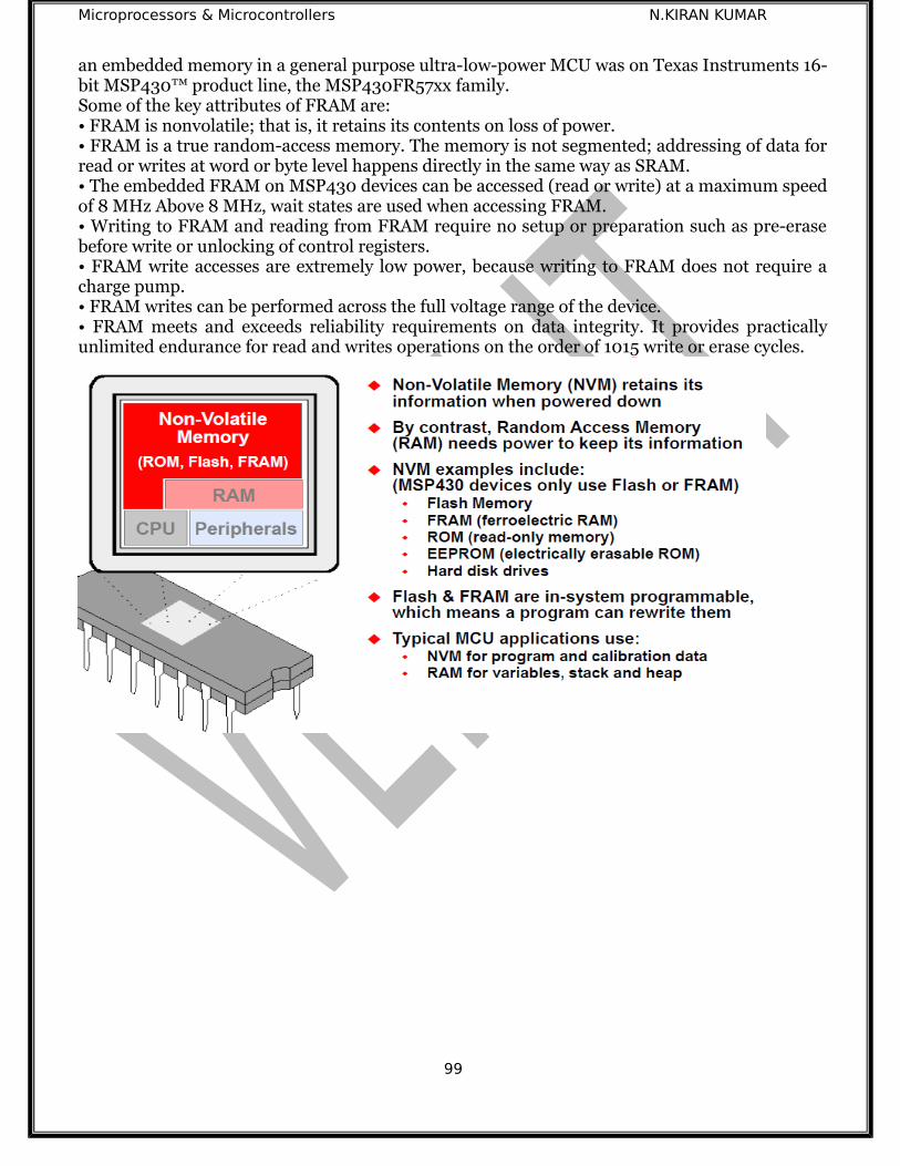
Microprocessors & Microcontrollers N.KIRAN KUMAR
an embedded memory in a general purpose ultra-low-power MCU was on Texas Instruments 16-bit MSP430™ product line, the MSP430FR57xx family.Some of the key attributes of FRAM are:• FRAM is nonvolatile; that is, it retains its contents on loss of power.• FRAM is a true random-access memory. The memory is not segmented; addressing of data forread or writes at word or byte level happens directly in the same way as SRAM.• The embedded FRAM on MSP430 devices can be accessed (read or write) at a maximum speedof 8 MHz Above 8 MHz, wait states are used when accessing FRAM. • Writing to FRAM and reading from FRAM require no setup or preparation such as pre-erasebefore write or unlocking of control registers.• FRAM write accesses are extremely low power, because writing to FRAM does not require acharge pump.• FRAM writes can be performed across the full voltage range of the device.• FRAM meets and exceeds reliability requirements on data integrity. It provides practicallyunlimited endurance for read and writes operations on the order of 1015 write or erase cycles.
99

Microprocessors & Microcontrollers N.KIRAN KUMAR
Timers:Timers produce delays. These delays are unpredictable. So reference time is required.
The reference of time can be produced by counter which counts fixed number of time. Actual time can be obtained by multiplying counter with clock interval time. The accuracy and stability of a clock should be critical.Timers can be used for:
Generates fixed time period events Allows a periodic wakeup from sleep mode Counts signal edges Replace delay loops
Timers can have different forms: Watchdog timers Basic Timer1 Basic Timer2 RTC
100
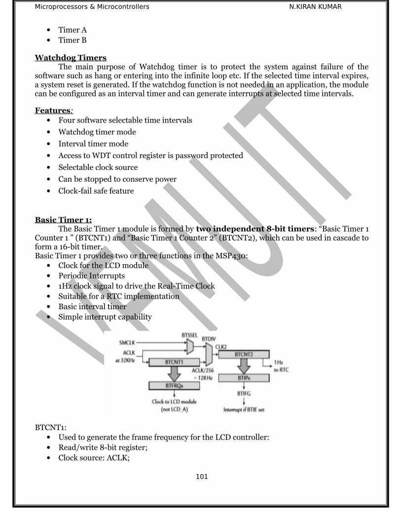
Microprocessors & Microcontrollers N.KIRAN KUMAR
Timer A Timer B
Watchdog TimersThe main purpose of Watchdog timer is to protect the system against failure of the
software such as hang or entering into the infinite loop etc. If the selected time interval expires,a system reset is generated. If the watchdog function is not needed in an application, the modulecan be configured as an interval timer and can generate interrupts at selected time intervals.
Features : Four software selectable time intervals
Watchdog timer mode
Interval timer mode
Access to WDT control register is password protected
Selectable clock source
Can be stopped to conserve power
Clock-fail safe feature
Basic Timer 1:The Basic Timer 1 module is formed by two independent 8-bit timers: “Basic Timer 1
Counter 1 ” (BTCNT1) and “Basic Timer 1 Counter 2” (BTCNT2), which can be used in cascade toform a 16-bit timer. Basic Timer 1 provides two or three functions in the MSP430:
Clock for the LCD module Periodic Interrupts 1Hz clock signal to drive the Real-Time Clock Suitable for a RTC implementation Basic interval timer Simple interrupt capability
BTCNT1: Used to generate the frame frequency for the LCD controller: Read/write 8-bit register; Clock source: ACLK;
101
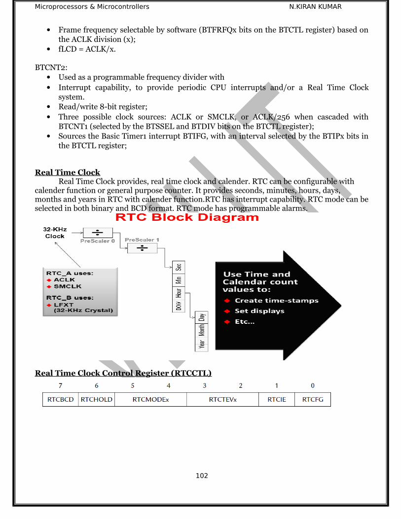
Microprocessors & Microcontrollers N.KIRAN KUMAR
Frame frequency selectable by software (BTFRFQx bits on the BTCTL register) based onthe ACLK division (x);
fLCD = ACLK/x.
BTCNT2: Used as a programmable frequency divider with Interrupt capability, to provide periodic CPU interrupts and/or a Real Time Clock
system. Read/write 8-bit register; Three possible clock sources: ACLK or SMCLK, or ACLK/256 when cascaded with
BTCNT1 (selected by the BTSSEL and BTDIV bits on the BTCTL register); Sources the Basic Timer1 interrupt BTIFG, with an interval selected by the BTIPx bits in
the BTCTL register;
Real Time ClockReal Time Clock provides, real time clock and calender. RTC can be configurable with
calender function or general purpose counter. It provides seconds, minutes, hours, days, months and years in RTC with calender function.RTC has interrupt capability. RTC mode can beselected in both binary and BCD format. RTC mode has programmable alarms.
Real Time Clock Control Register (RTCCTL)
102
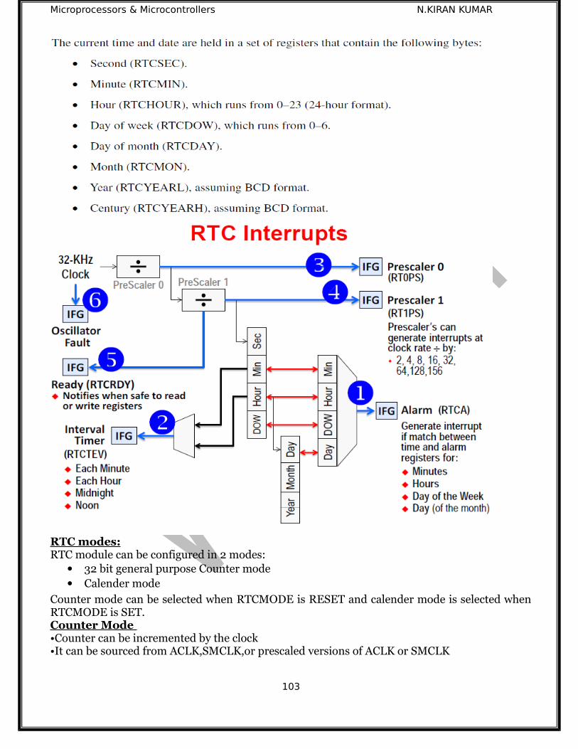
Microprocessors & Microcontrollers N.KIRAN KUMAR
RTC modes:RTC module can be configured in 2 modes:
32 bit general purpose Counter mode Calender mode
Counter mode can be selected when RTCMODE is RESET and calender mode is selected whenRTCMODE is SET.Counter Mode •Counter can be incremented by the clock •It can be sourced from ACLK,SMCLK,or prescaled versions of ACLK or SMCLK
103

Microprocessors & Microcontrollers N.KIRAN KUMAR
•Prescaled version of ACLK or SMCLK are sourced from the prescale dividers•The output ofRT0PS can be cascaded with RT1PS. •The cascaded output can be used as a clock source input to the 32-bit counter Calendar Mode •RTCMODE is set •It provides seconds, minutes,hours, day of week,day of month,month and year •In selectable BCD or Hexadecimal Format •Includes leap year algoritham[all years evenly divisible by four] •RT0PS is sourced from ACLK[32.768KHz for RTC_A Calendar operation] •RT1PS is cascaded with the output ACLK/256 of RT0PS Real time clock alarm Function•The RTC_A module provides for a flexible alarm system•The user-programmable alarm function is only available in the calendar mode of operation.•Each alarm register contains an alarm enable (AE) bit that can be used to enable the respectivealarm register.•By setting AE bits of the various alarm registers, a variety of alarm events can be generated.Timers:MSP430 microcontroller has following timer features
16-bit Timer/Counter 3-bit Prescaler 3 Capture/Compare Registers Four Modes Stop, Up, Continuous, Up/Down Selectable Clock Source Configurable Outputs PWM Capable
There are two main parts to the Timer hardware:
Timer block: The core, based on the 16-bit register TAR. There is a choice of sources for theclock, whose frequency can be divided down (prescaled). The timer block has no output but aflag TAIFG is raised when the counter returns to 0.
Capture/compare channels: In which most events occur, each of which is based on a registerTACCRn. They all work in the same way with the important exception of TACCR0.
Each channel can
Capture an input, which means recording the “time” (the value in TAR) at which the inputchanges in TACCRn; the input can be either external or internal from another peripheral orsoftware.
Compare the current value of TAR with the value stored in TACCRn and update an outputwhen they match; the output can again be either external or internal.
Request an interrupt by setting its flag TACCRn CCIFG on either of these events; this can bedone even if no output signal is produced.
Sample an input at a compare event; this special feature is particularly useful if Timer_A is
104

Microprocessors & Microcontrollers N.KIRAN KUMAR
used for serial communication in a device that lacks a dedicated interface.
Timer Block:
This contains the 16-bit timer register TAR, which is central to the operation of the timer. It is controlled by the register TACTL shown in Figure.
Remember that a timer is really no more than a counter and has no direct concept of time(the Real-Time Clock is an exception). It is the programmer’s job to establish a relation between the value in the counter and real time. This depends essentially on the frequency of theclock for the timer. It can be chosen from four sources by using the TASSELx bits
SMCLK is internal and usually fast (megahertz).
ACLK is internal and usually slow, typically 32 KHz from a watch crystal .
TACLK is external.
INCLK is also external, sometimes a separate pin but often it is connected through an inverter to the pin for TACLK so that INCLK = TACLK.
The frequency of the incoming clock can be divided down by 2, 4, or 8 if desired by configuring the IDx bits.Capture: When a capture input signal occurs, a snapshot of the counter register is captured. It is copied into a capture register (CCR). Overflow occurs when indicate 2nd capture to CCR before 1st was read. There are 7 captures registers (CR0-CR6).
105
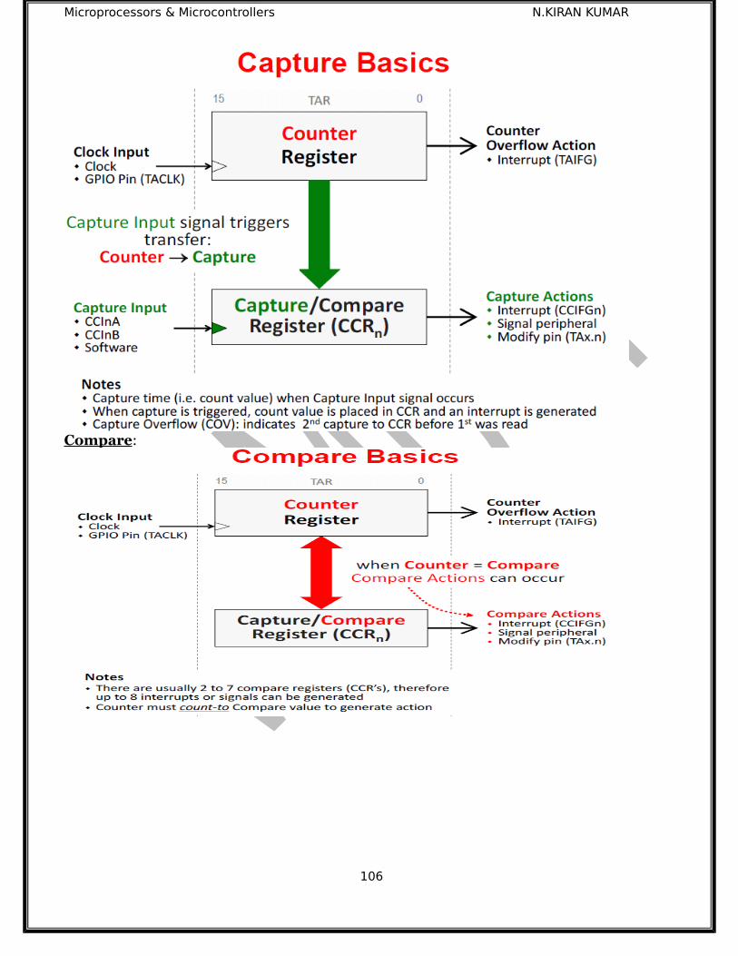
Microprocessors & Microcontrollers N.KIRAN KUMAR
Compare:
106
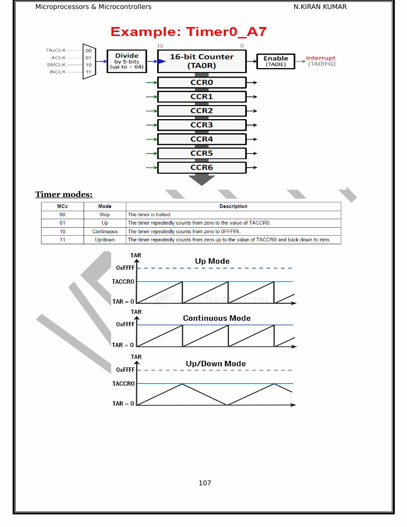
Microprocessors & Microcontrollers N.KIRAN KUMAR
Timer modes:
107
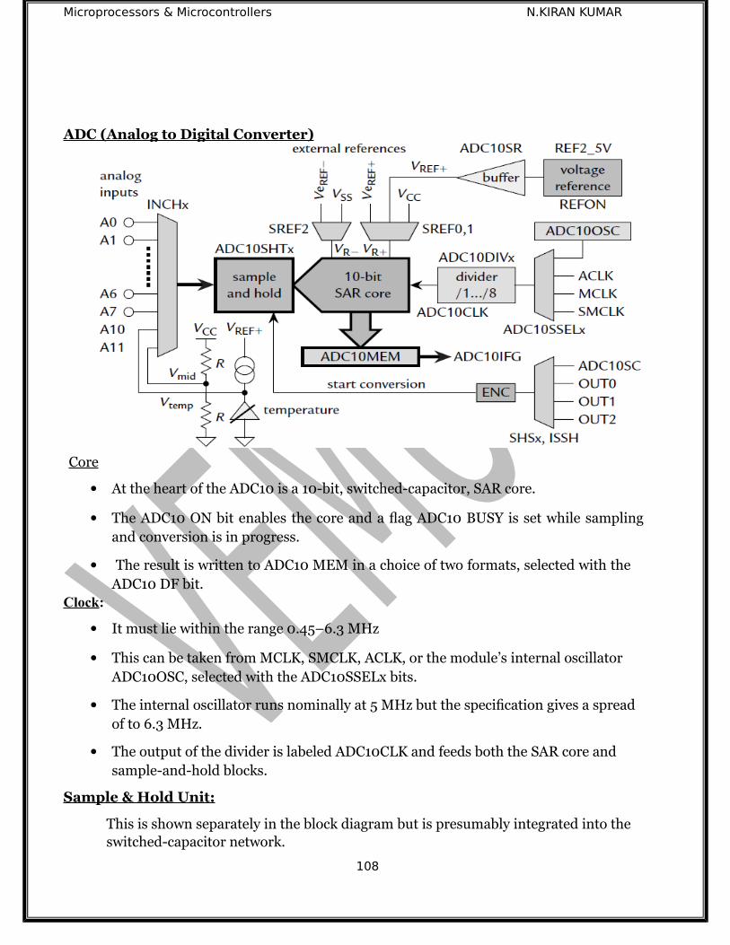
Microprocessors & Microcontrollers N.KIRAN KUMAR
ADC (Analog to Digital Converter)
Core
At the heart of the ADC10 is a 10-bit, switched-capacitor, SAR core.
The ADC10 ON bit enables the core and a flag ADC10 BUSY is set while samplingand conversion is in progress.
The result is written to ADC10 MEM in a choice of two formats, selected with theADC10 DF bit.
Clock:
It must lie within the range 0.45–6.3 MHz
This can be taken from MCLK, SMCLK, ACLK, or the module’s internal oscillator ADC10OSC, selected with the ADC10SSELx bits.
The internal oscillator runs nominally at 5 MHz but the specification gives a spread of to 6.3 MHz.
The output of the divider is labeled ADC10CLK and feeds both the SAR core and sample-and-hold blocks.
Sample & Hold Unit:
This is shown separately in the block diagram but is presumably integrated into the switched-capacitor network.
108

Microprocessors & Microcontrollers N.KIRAN KUMAR
The time is chosen with the ADC10SHTx bits, which allow 4, 8, 16, or 64 cycles of ADC10CLK.
Input Selection
A multiplexer selects the input from eight external pins A0–A7 (more in largerMSP430s) and four internal connections.Two of the internal connections are for optional, external reference voltages.The other two internal connections are A10 to a temperature sensor and A11 to Vmid
= ½ (VCC + VSS), which is provided to monitor the supply voltage.
Conversion Trigger A conversion can be triggered in two ways provided that the ENC bit is set. The first is by
setting the ADC10SC bit from software. Conversion is normally triggered by a rising edge on the input but this can be inverted
with the ISSH bit.
Voltage References and BufferThe ADC10 is slightly unusual because it uses references for both ends of the range; the
lower limit need not be ground (VSS). There are two choices for the lower reference, selected with the SREF2 bit:
The default is analog ground, AV SS.
An external reference VeREF− can be applied directly to the SAR core without buffering.
There is more choice for the upper reference, selected with SREF0 and SREF1:
The default is the analog supply voltage, AVCC.
An internal reference voltage VREF+ is enabled with REFON.
An external reference VeREF+ can be applied directly to the SAR core.
The external reference can also be buffered.
No external capacitors are needed for the internal voltage reference, whether it is used internallyor externally.
Interrupts
The interrupt flag ADC10IFG is raised when the result is written to ADC10MEM except when the DTC is used, when it is set after a block has been completed
Basic operation of the ADC 10:
1. Configure the ADC10, including the ADC10ON bit to enable the module. The ENC bit must be clear during this operation because most bits in ADC10CTL0 and ADC10CTL1 can be changed only when ENC = 0.
2. Set the ENC bit to enable a conversion. This cannot be done while the module is being configured in the previous step.
3. Trigger the conversion, either by setting the ADC10SC bit or by an edge from Timer_A.
4. The last two steps must be repeated for each conversion, which requires clearing and
109
Microprocessors & Microcontrollers N.KIRAN KUMAR
setting the ENC bit again.
5. The input to the ADC10 is selected with the INCHx bits in ADC10CTL1.
UNIT V
Universal Serial Communication Interface (USCI) OverviewThe USCI modules support multiple serial communication modes. Different
USCI modules support different modes. Each different USCI module is named with adifferent letter. For example, USCI_A is different from USCI_B, etc. If more than oneidentical USCI module is implemented on one device, those modules are named withincrementing numbers. For example, if one device has two USCI_A modules, they arenamed USCI_A0 and USCI_A1. See the device-specific data sheet to determine whichUSCI modules, if any, are implemented on which devices.USCI_Ax modules support:
• UART mode• Pulse shaping for IrDA communications• Automatic baud-rate detection for LIN communications• SPI
mode USCI_Bx modules support:
• I2C mode• SPI mode
USCI Introduction – UART Mode
In asynchronous mode, the USCI_Ax modules connect the device to anexternal system via two external pins, UCAxRXD and UCAxTXD. UART mode isselected when the UCSYNC bit is cleared. UART mode features include:
• 7- or 8-bit data with odd, even, or non-parity• Independent transmit and receive shift registers• Separate transmit and receive buffer registers• LSB-first or MSB-first data transmit and receive• Built-in idle-line and address-bit communication protocols for multiprocessor systems• Receiver start-edge detection for auto wake up from LPMx modes (wake up from LPMx.5 is notsupported)• Programmable baud rate with modulation for fractional baud-rate support• Status flags for error detection and suppression• Status flags for address detection
USCI Operation – UART Mode
In UART mode, the USCI transmits and receives characters at a bit rate
110
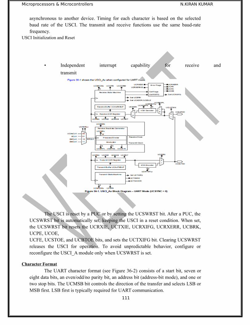
Microprocessors & Microcontrollers N.KIRAN KUMAR
asynchronous to another device. Timing for each character is based on the selectedbaud rate of the USCI. The transmit and receive functions use the same baud-ratefrequency.
USCI Initialization and Reset
• Independent interrupt capability for receive and
transmit
The USCI is reset by a PUC or by setting the UCSWRST bit. After a PUC, theUCSWRST bit is automatically set, keeping the USCI in a reset condition. When set,the UCSWRST bit resets the UCRXIE, UCTXIE, UCRXIFG, UCRXERR, UCBRK,UCPE, UCOE,UCFE, UCSTOE, and UCBTOE bits, and sets the UCTXIFG bit. Clearing UCSWRSTreleases the USCI for operation. To avoid unpredictable behavior, configure orreconfigure the USCI_A module only when UCSWRST is set.
Character Format
The UART character format (see Figure 36-2) consists of a start bit, seven oreight data bits, an even/odd/no parity bit, an address bit (address-bit mode), and one ortwo stop bits. The UCMSB bit controls the direction of the transfer and selects LSB orMSB first. LSB first is typically required for UART communication.
111
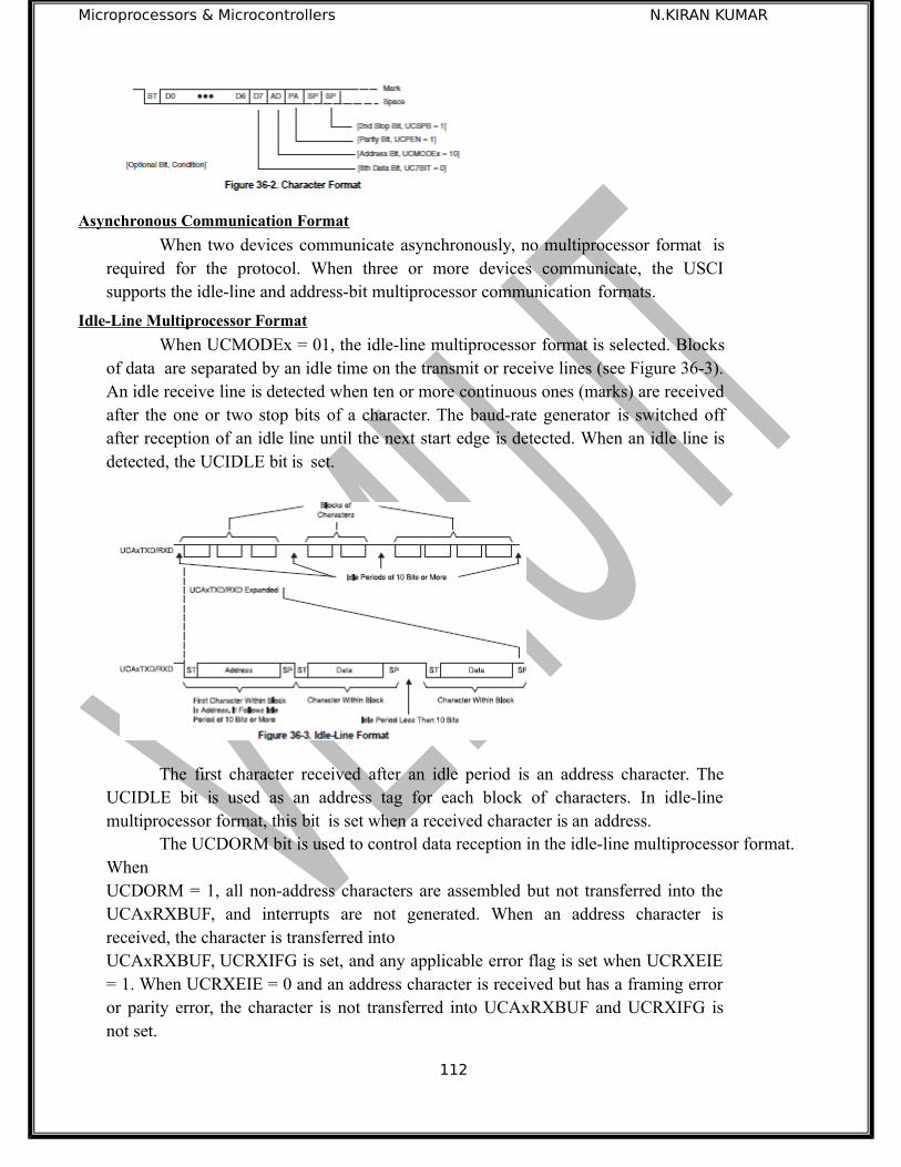
Microprocessors & Microcontrollers N.KIRAN KUMAR
Asynchronous Communication Format
When two devices communicate asynchronously, no multiprocessor format isrequired for the protocol. When three or more devices communicate, the USCIsupports the idle-line and address-bit multiprocessor communication formats.
Idle-Line Multiprocessor Format
When UCMODEx = 01, the idle-line multiprocessor format is selected. Blocksof data are separated by an idle time on the transmit or receive lines (see Figure 36-3).An idle receive line is detected when ten or more continuous ones (marks) are receivedafter the one or two stop bits of a character. The baud-rate generator is switched offafter reception of an idle line until the next start edge is detected. When an idle line isdetected, the UCIDLE bit is set.
The first character received after an idle period is an address character. TheUCIDLE bit is used as an address tag for each block of characters. In idle-linemultiprocessor format, this bit is set when a received character is an address.
The UCDORM bit is used to control data reception in the idle-line multiprocessor format.WhenUCDORM = 1, all non-address characters are assembled but not transferred into theUCAxRXBUF, and interrupts are not generated. When an address character isreceived, the character is transferred intoUCAxRXBUF, UCRXIFG is set, and any applicable error flag is set when UCRXEIE= 1. When UCRXEIE = 0 and an address character is received but has a framing erroror parity error, the character is not transferred into UCAxRXBUF and UCRXIFG isnot set.
112

Microprocessors & Microcontrollers N.KIRAN KUMAR
If an address is received, user software can validate the address and must resetUCDORM to continue receiving data. If UCDORM remains set, only addresscharacters are received. When UCDORM is cleared during the reception of a character,the receive interrupt flag is set after the reception completed. The UCDORM bit is notmodified by the USCI hardware automatically.
For address transmission in idle-line multiprocessor format, a precise idleperiod can be generated by the USCI to generate address character identifiers onUCAxTXD. The double- buffered UCTXADDR flag indicates if the next characterloaded into UCAxTXBUF is preceded by an idle line of 11 bits. UCTXADDR isautomatically cleared when the start bit is generated.
Transmitting an Idle Frame
The following procedure sends out an idle frame to indicate an addresscharacter followed by associated data:
1. Set UCTXADDR, then write the address character to UCAxTXBUF.UCAxTXBUF must be ready fornew data (UCTXIFG = 1). This generates an idle period of exactly 11 bitsfollowed by the address character. UCTXADDR is reset automatically whenthe address character is transferred from UCAxTXBUF into the shift register.2. Write desired data characters to UCAxTXBUF. UCAxTXBUF must be readyfor new data (UCTXIFG =1). The data written to UCAxTXBUF is transferred to the shift register andtransmitted as soon as the shift register is ready for new data. The idle-line timemust not be exceeded between address and data transmission or between datatransmissions. Otherwise, the transmitted data is misinterpreted as an address
Address-Bit Multiprocessor Format
When UCMODEx = 10, the address-bit multiprocessor format is selected.Each processed character contains an extra bit used as an address indicator (see Figure36-4). The first character in a block of characters carries a set address bit that indicatesthat the character is an address. The USCI UCADDR bit is set when a receivedcharacter has its address bit set and is transferred to UCAxRXBUF.
The UCDORM bit is used to control data reception in the address-bitmultiprocessor format. When UCDORM is set, data characters with address bit = 0 areassembled by the receiver but are not transferred to UCAxRXBUF and no interruptsare generated. When a character containing a set address bit is received, the character istransferred into UCAxRXBUF, UCRXIFG is set, and any applicable error flag is setwhen UCRXEIE = 1. When UCRXEIE = 0 and a character containing a set address bitis received but has a framing error or parity error, the character is not transferred intoUCAxRXBUF andUCRXIFG is not set.
If an address is received, user software can validate the address and must resetUCDORM to continue receiving data. If UCDORM remains set, only address
113

Microprocessors & Microcontrollers N.KIRAN KUMAR
characters with address bit = 1 are received. The UCDORM bit is not modified by theUSCI hardware automatically.
When UCDORM = 0, all received characters set the receive interrupt flagUCRXIFG. If UCDORM is cleared during the reception of a character, the receiveinterrupt flag is set after the reception is completed.
For address transmission in address-bit multiprocessor mode, the address bit ofa character is controlled by the UCTXADDR bit. The value of the UCTXADDR bit isloaded into the address bit of the character transferred from UCAxTXBUF to thetransmit shift register. UCTXADDR is automatically cleared when the start bit isgenerated.
Break Reception and Generation
When UCMODEx = 00, 01, or 10, the receiver detects a break when all data,parity, and stop bits are low, regardless of the parity, address mode, or other charactersettings. When a break is detected, the UCBRK bit is set. If the break interrupt enablebit (UCBRKIE) is set, the receive interrupt flag UCRXIFG is also set.
114
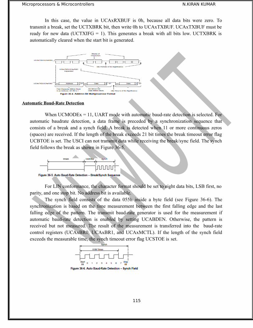
Microprocessors & Microcontrollers N.KIRAN KUMAR
In this case, the value in UCAxRXBUF is 0h, because all data bits were zero. Totransmit a break, set the UCTXBRK bit, then write 0h to UCAxTXBUF. UCAxTXBUF must beready for new data (UCTXIFG = 1). This generates a break with all bits low. UCTXBRK isautomatically cleared when the start bit is generated.
Automatic Baud-Rate Detection
When UCMODEx = 11, UART mode with automatic baud-rate detection is selected. Forautomatic baudrate detection, a data frame is preceded by a synchronization sequence thatconsists of a break and a synch field. A break is detected when 11 or more continuous zeros(spaces) are received. If the length of the break exceeds 21 bit times the break timeout error flagUCBTOE is set. The USCI can not transmit data while receiving the break/sync field. The synchfield follows the break as shown in Figure 36-5.
For LIN conformance, the character format should be set to eight data bits, LSB first, noparity, and one stop bit. No address bit is available.
The synch field consists of the data 055h inside a byte field (see Figure 36-6). Thesynchronization is based on the time measurement between the first falling edge and the lastfalling edge of the pattern. The transmit baud-rate generator is used for the measurement ifautomatic baud-rate detection is enabled by setting UCABDEN. Otherwise, the pattern isreceived but not measured. The result of the measurement is transferred into the baud-ratecontrol registers (UCAxBR0, UCAxBR1, and UCAxMCTL). If the length of the synch fieldexceeds the measurable time, the synch timeout error flag UCSTOE is set.
115

Microprocessors & Microcontrollers N.KIRAN KUMAR
The UCDORM bit is used to control data reception in this mode. When UCDORM isset, all characters are received but not transferred into the UCAxRXBUF, and interrupts are notgenerated. When a break/synch field is detected, the UCBRK flag is set. The characterfollowing the break/synch field is transferred into UCAxRXBUF and the UCRXIFG interruptflag is set. Any applicable error flag is also set. If the UCBRKIE bit is set, reception of thebreak/synch sets the UCRXIFG. The UCBRK bit is reset by user software or by reading thereceive buffer UCAxRXBUF.
When a break/synch field is received, user software must reset UCDORM to continuereceiving data. If UCDORM remains set, only the character after the next reception of abreak/synch field is received. The UCDORM bit is not modified by the USCI hardwareautomatically. When UCDORM = 0, all received characters set the receive interrupt flagUCRXIFG. If UCDORM is cleared during the reception of a character, the receive interrupt flagis set after the reception is complete.
The counter used to detect the baud rate is limited to 07FFFh (32767) counts. Thismeans the minimum baud rate detectable is 488 baud in oversampling mode and 30 baud inlow- frequency mode.The automatic baud-rate detection mode can be used in a full-duplex communication systemwith some restrictions. The USCI can not transmit data while receiving the break/sync field and,if a 0h byte with framing error is received, any data transmitted during this time gets corrupted.The latter case can be discovered by checking the received data and the UCFE bit.
Transmitting a Break/Synch Field
The following procedure transmits a break/synch field:1. Set UCTXBRK with UMODEx = 11.2. Write 055h to UCAxTXBUF. UCAxTXBUF must be ready for new data (UCTXIFG = 1).This generates a break field of 13 bits followed by a break delimiter and the synchcharacter. The length of the break delimiter is controlled with the UCDELIMx bits.UCTXBRK is reset automatically when the synch character is transferred fromUCAxTXBUF into the shift register.3. Write desired data characters to UCAxTXBUF. UCAxTXBUF must be ready for new data(UCTXIFG = 1).The data written to UCAxTXBUF is transferred to the shift register and transmitted as soon as the shift register is ready for new data.
IrDA Encoding and Decoding
When UCIREN is set, the IrDA encoder and decoder are enabled and provide hardwarebit shaping for IrDA communication.IrDA Encoding The encoder sends a pulse for every zero bit in the transmit bitstream coming from the UART
(see Figure 36-7). The pulse duration is defined by UCIRTXPLx bits specifying the number ofone-half clock periods of the clock selected by UCIRTXCLK.
116
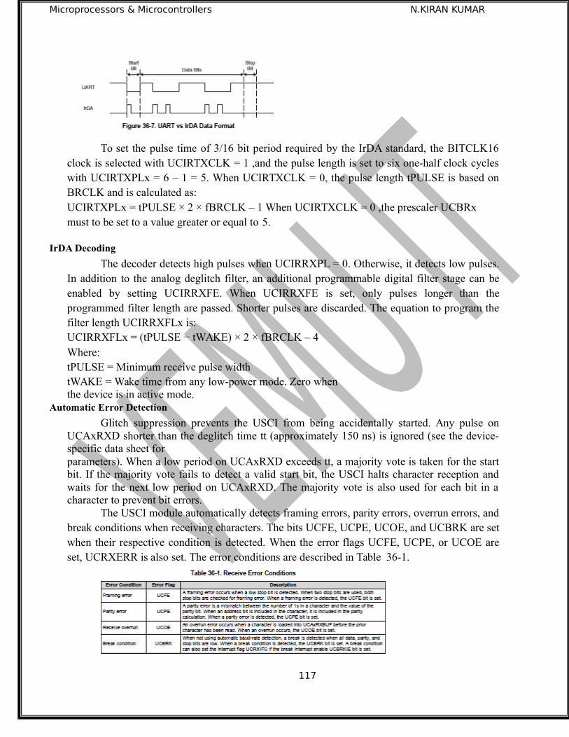
Microprocessors & Microcontrollers N.KIRAN KUMAR
To set the pulse time of 3/16 bit period required by the IrDA standard, the BITCLK16clock is selected with UCIRTXCLK = 1 ,and the pulse length is set to six one-half clock cycleswith UCIRTXPLx = 6 – 1 = 5. When UCIRTXCLK = 0, the pulse length tPULSE is based onBRCLK and is calculated as:UCIRTXPLx = tPULSE × 2 × fBRCLK – 1 When UCIRTXCLK = 0 ,the prescaler UCBRx must to be set to a value greater or equal to 5.
IrDA Decoding
The decoder detects high pulses when UCIRRXPL = 0. Otherwise, it detects low pulses.In addition to the analog deglitch filter, an additional programmable digital filter stage can beenabled by setting UCIRRXFE. When UCIRRXFE is set, only pulses longer than theprogrammed filter length are passed. Shorter pulses are discarded. The equation to program thefilter length UCIRRXFLx is:UCIRRXFLx = (tPULSE − tWAKE) × 2 × fBRCLK – 4Where:tPULSE = Minimum receive pulse widthtWAKE = Wake time from any low-power mode. Zero when the device is in active mode.
Automatic Error Detection
Glitch suppression prevents the USCI from being accidentally started. Any pulse onUCAxRXD shorter than the deglitch time tt (approximately 150 ns) is ignored (see the device-specific data sheet forparameters). When a low period on UCAxRXD exceeds tt, a majority vote is taken for the startbit. If the majority vote fails to detect a valid start bit, the USCI halts character reception andwaits for the next low period on UCAxRXD. The majority vote is also used for each bit in acharacter to prevent bit errors.
The USCI module automatically detects framing errors, parity errors, overrun errors, andbreak conditions when receiving characters. The bits UCFE, UCPE, UCOE, and UCBRK are setwhen their respective condition is detected. When the error flags UCFE, UCPE, or UCOE areset, UCRXERR is also set. The error conditions are described in Table 36-1.
117

Microprocessors & Microcontrollers N.KIRAN KUMAR
When UCRXEIE = 0 and a framing error or parity error is detected, no character isreceived intoUCAxRXBUF. When UCRXEIE = 1, characters are received into UCAxRXBUF and anyapplicable error bit is set. When any of the UCFE, UCPE, UCOE, UCBRK, or UCRXERR bit isset, the bit remains set until user software resets it or UCAxRXBUF is read. UCOE must bereset by reading UCAxRXBUF. Otherwise, it does not function properly. To detect overflowsreliably the following flow is recommended. After a character was received and UCAxRXIFG isset, first read UCAxSTAT to check the error flags including the overflow flag UCOE. ReadUCAxRXBUF next. This clears all error flags except UCOE, if UCAxRXBUF was overwrittenbetween the read access to UCAxSTAT and to UCAxRXBUF. Therefore, the UCOE flag shouldbe checked after reading UCAxRXBUF to detect this condition. Note that, in this case, theUCRXERR flag is not set.
USCI Receive Enable
The USCI module is enabled by clearing the UCSWRST bit and the receiver is ready andin an idle state. The receive baud rate generator is in a ready state but is not clocked norproducing any clocks.The falling edge of the start bit enables the baud rate generator and the UART state machinechecks for a valid start bit. If no valid start bit is detected the UART state machine returns to itsidle state and the baud rate generator is turned off again. If a valid start bit is detected, acharacter is received.
When the idle-line multiprocessor mode is selected with UCMODEx = 01 the UARTstate machine checks for an idle line after receiving a character. If a start bit is detected anothercharacter is received. Otherwise the UCIDLE flag is set after 10 ones are received and theUART state machine returns to its idle state and the baud rate generator is turned off.
Receive Data Glitch Suppression
Glitch suppression prevents the USCI from being accidentally started. Any glitch onUCAxRXD shorter than the deglitch time tt (approximately 150 ns) is ignored by the USCI, andfurther action is initiated as shown in Figure 36-8 (see the device-specific data sheet forparameters).
When a glitch is longer than tt, or a valid start bit occurs on UCAxRXD, the USCI receiveoperation is started and a majority vote is taken (see Figure 36-9). If the majority vote fails todetect a start bit, the USCI halts character reception.
118
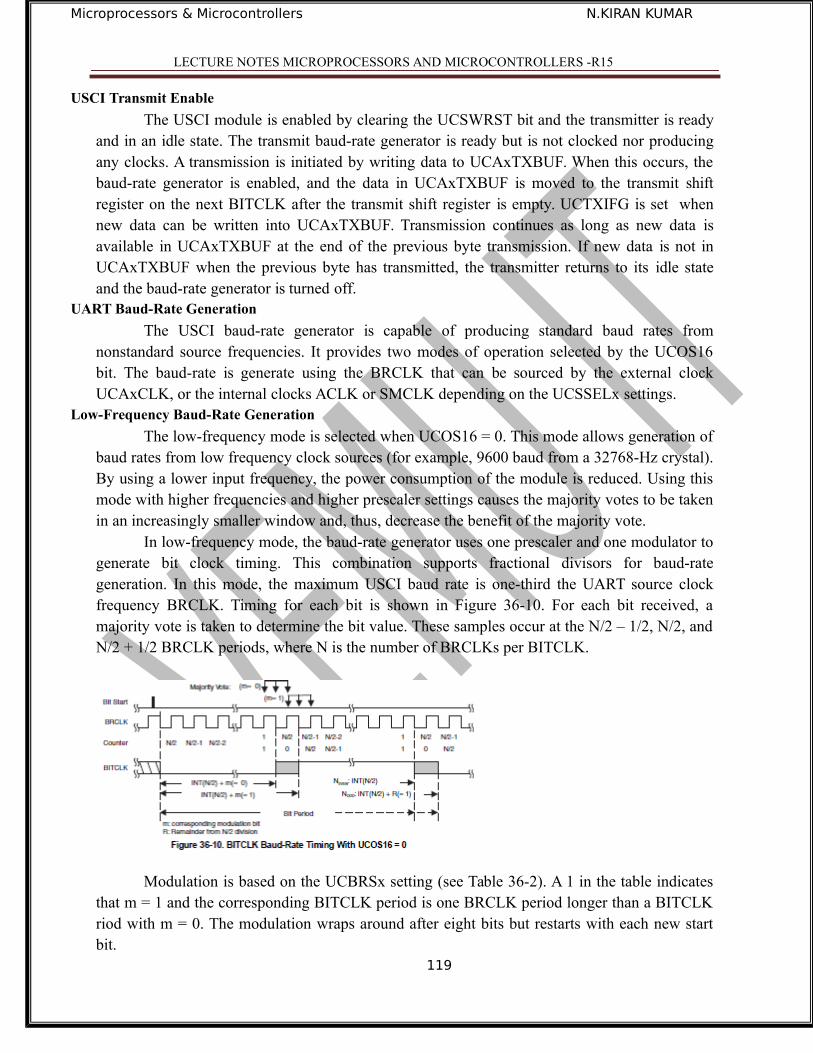
Microprocessors & Microcontrollers N.KIRAN KUMAR
LECTURE NOTES MICROPROCESSORS AND MICROCONTROLLERS -R15
USCI Transmit Enable
The USCI module is enabled by clearing the UCSWRST bit and the transmitter is readyand in an idle state. The transmit baud-rate generator is ready but is not clocked nor producingany clocks. A transmission is initiated by writing data to UCAxTXBUF. When this occurs, thebaud-rate generator is enabled, and the data in UCAxTXBUF is moved to the transmit shiftregister on the next BITCLK after the transmit shift register is empty. UCTXIFG is set whennew data can be written into UCAxTXBUF. Transmission continues as long as new data isavailable in UCAxTXBUF at the end of the previous byte transmission. If new data is not inUCAxTXBUF when the previous byte has transmitted, the transmitter returns to its idle stateand the baud-rate generator is turned off.
UART Baud-Rate Generation
The USCI baud-rate generator is capable of producing standard baud rates fromnonstandard source frequencies. It provides two modes of operation selected by the UCOS16bit. The baud-rate is generate using the BRCLK that can be sourced by the external clockUCAxCLK, or the internal clocks ACLK or SMCLK depending on the UCSSELx settings.
Low-Frequency Baud-Rate Generation
The low-frequency mode is selected when UCOS16 = 0. This mode allows generation ofbaud rates from low frequency clock sources (for example, 9600 baud from a 32768-Hz crystal).By using a lower input frequency, the power consumption of the module is reduced. Using thismode with higher frequencies and higher prescaler settings causes the majority votes to be takenin an increasingly smaller window and, thus, decrease the benefit of the majority vote.
In low-frequency mode, the baud-rate generator uses one prescaler and one modulator togenerate bit clock timing. This combination supports fractional divisors for baud-rategeneration. In this mode, the maximum USCI baud rate is one-third the UART source clockfrequency BRCLK. Timing for each bit is shown in Figure 36-10. For each bit received, amajority vote is taken to determine the bit value. These samples occur at the N/2 – 1/2, N/2, andN/2 + 1/2 BRCLK periods, where N is the number of BRCLKs per BITCLK.
Modulation is based on the UCBRSx setting (see Table 36-2). A 1 in the table indicatesthat m = 1 and the corresponding BITCLK period is one BRCLK period longer than a BITCLKriod with m = 0. The modulation wraps around after eight bits but restarts with each new startbit.
119

Microprocessors & Microcontrollers N.KIRAN KUMAR
120

Microprocessors & Microcontrollers N.KIRAN KUMAR
Oversampling Baud-Rate Generation
The oversampling mode is selected when UCOS16 = 1. This mode supports sampling aUART bitstream with higher input clock frequencies. This results in majority votes that arealways 1/16 of a bit clock period apart. This mode also easily supports IrDA pulses with a 3/16bit time when the IrDA encoder and decoder are enabled.
This mode uses one prescaler and one modulator to generate the BITCLK16 clock that is16 times faster than the BITCLK. An additional divider and modulator stage generates BITCLKfrom BITCLK16. This combination supports fractional divisions of both BITCLK16 andBITCLK for baud-rate generation. In this mode, the maximum USCI baud rate is 1/16 theUART source clock frequency BRCLK. When UCBRx is set to 0 or 1, the first prescaler andmodulator stage is bypassed and BRCLK is equal to BITCLK16 – in this case, no modulationfor the BITCLK16 is possible and, thus, the UCBRFx bits are ignored. Modulation forBITCLK16 is based on the UCBRFx setting (see Table 36-3). A 1 in the table indicates that thecorresponding BITCLK16 period is one BRCLK period longer than the periods m = 0. Themodulation restarts with each new bit timing. Modulation for BITCLK is based on the UCBRSxsetting (see Table 36-2) as previously described.
Setting a Baud Rate
For a given BRCLK clock source, the baud rate used determines the required division factor N:
N = fBRCLK/Baudrate The division factor N is often a noninteger value, thus, at least one dividerand one modulator stage is used to meet the factor as closely as possible. If N is equal or greaterthan 16, the oversampling baud-rate generation mode can be chosen by setting COS16.
121
Microprocessors & Microcontrollers N.KIRAN KUMAR
Low-Frequency Baud-Rate Mode Setting
In low-frequency mode, the integer portion of the divisor is realized by the prescaler: UCBRx = INT(N) and the fractional portion is realized by the modulator with the following nominal formula: UCBRSx = round[( N – INT(N)) × 8] Incrementing or decrementing the UCBRSx setting by one count may give a lower maximum bit error for any given bit. To determine if this is the case, a detailed error calculation must be performed for each bit for each UCBRSx setting.
Oversampling Baud-Rate Mode Setting
In the oversampling mode, the prescaler is set to: UCBRx = INT(N/16) and the firststage modulator is set to: UCBRFx = round([(N/16) – INT(N/16)] × 16)
When greater accuracy is required, the UCBRSx modulator can also be implementedwith values from 0 to 7. To find the setting that gives the lowest maximum bit error rate for anygiven bit, a detailed error calculation must be performed for all settings of UCBRSx from 0 to 7with the initial UCBRFx setting, and with the UCBRFx setting incremented and decremented byone.
Transmit Bit Timing
The timing for each character is the sum of the individual bit timings. Using themodulation features of the baud-rate generator reduces the cumulative bit error. The individualbit error can be calculated using the following steps.
Receive Bit Timing
Receive timing error consists of two error sources. The first is the bit-to-bit timing errorsimilar to the transmit bit timing error. The second is the error between a start edge occurringand the start edge being accepted by the USCI module. Figure 36-11 shows the asynchronous
122

Microprocessors & Microcontrollers N.KIRAN KUMAR
timing errors between data on the UCAxRXD pin and the internal baud-rate clock. This resultsin an additional synchronization error. The synchronization error tSYNC is between –0.5BRCLKs and +0.5 RCLKs, independent of the selected baudrate generation mode.
Using the USCI Module in UART Mode With Low-Power Modes
The USCI module provides automatic clock activation for use with low-power modes.When the USCI clock source is inactive because the device is in a low-power mode, the USCImodule automatically activates it when needed, regardless of the control-bit settings for theclock source. The clock remains active until the USCI module returns to its idle condition. Afterthe USCI module returns to the idle condition, control of the clock source reverts to the settingsof its control bits.
USCI Interrupts in UART Mode
The USCI has only one interrupt vector that is shared for transmission and for reception.USCI_Ax and USC_Bx do not share the same interrupt vector.
UART Transmit Interrupt Operation
The UCTXIFG interrupt flag is set by the transmitter to indicate that UCAxTXBUF isready to accept another character. An interrupt request is generated if UCTXIE and GIE are alsoset. UCTXIFG is automatically reset if a character is written to UCAxTXBUF. UCTXIFG is setafter a PUC or when UCSWRST = 1. UCTXIE is reset after a PUC or when UCSWRST = 1.
UART Receive Interrupt Operation
The UCRXIFG interrupt flag is set each time a character is received and loaded intoUCAxRXBUF. An interrupt request is generated if UCRXIE and GIE are also set. UCRXIFGand UCRXIE are reset by a system reset PUC signal or when UCSWRST = 1. UCRXIFG isautomatically reset when UCAxRXBUF is read.Additional interrupt control features include:
• When UCAxRXEIE = 0, erroneous characters do not set UCRXIFG.• When UCDORM = 1, nonaddress characters do not set UCRXIFG in multiprocessor modes. In plainUART mode, no characters are set UCRXIFG.• When UCBRKIE = 1, a break condition sets the UCBRK bit and the UCRXIFG flag.
UCAxIV,
Interrupt Vector Generator
The USCI interrupt flags are prioritized and combined to source a single interrupt vector.The interrupt vector register UCAxIV is used to determine which flag requested an interrupt.The highest-priority enabled interrupt generates a number in the UCAxIV register that can beevaluated or added to the program counter to automatically enter the appropriate software
routine. Disabled interrupts do not affect the UCAxIV value. Any access, read or write, of theUCAxIV register automatically resets the highest-pending interrupt flag. If another interruptflag is set, another interrupt is immediately generated after servicing the initial interrupt.
USB Introduction
The features of the USB module include:
123
Microprocessors & Microcontrollers N.KIRAN KUMAR
• Fully compliant with the USB 2.0 full-speed specification– Full-speed device (12 Mbps) with integrated USB transceiver (PHY)– Up to eight input and eight output endpoints– Supports control, interrupt, and bulk transfers– Supports USB suspend, resume, and remote wakeup
• A power supply system independent from the PMM system– Integrated 3.3-V LDO regulator with sufficient output to power entire MSP430 and system circuitryfrom 5-V VBUS– Integrated 1.8-V LDO regulator for PHY and PLL– Easily used in either bus-powered or self-powered operation– Current-limiting capability on 3.3-V LDO output– Autonomous power-up of device on arrival of USB power possible (low or no battery condition)
• Internal 48-MHz USB clock– Integrated programmable PLL– Highly-flexible input clock frequencies for use with lowest-cost crystals
• 1904 bytes of dedicated USB buffer space for endpoints, with fully configurable size to a granularity ofeight bytes• Timestamp generator with 62.5-ns resolution• When USB is disabled
– Buffer space is mapped into general RAM, providing additional 2KB to the system– USB interface pins become high-current general purpose I/O pins
NOTE: Use of the word deviceThe word device is used throughout the chapter. This word can mean one of two things,
depending on the context. In a USB context, it means what the USB specification refers to as adevice, function, or peripheral; that is, a piece of equipment that can be attached to a USB hostor hub. In a semiconductor context, it refers to an integrated circuit such as then MSP430. Toavoid confusion, the term USB device in this document refers to the USB-context meaning ofthe word. The word device by itself refers to silicon devices such as the MSP430.Figure 42-1 shows a block diagram of the USB module.
124
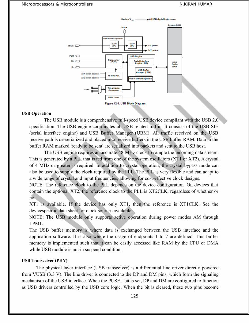
Microprocessors & Microcontrollers N.KIRAN KUMAR
USB Operation
The USB module is a comprehensive full-speed USB device compliant with the USB 2.0specification. The USB engine coordinates all USB-related traffic. It consists of the USB SIE(serial interface engine) and USB Buffer Manager (UBM). All traffic received on the USBreceive path is de-serialized and placed into receive buffers in the USB buffer RAM. Data in thebuffer RAM marked 'ready to be sent' are serialized into packets and sent to the USB host.
The USB engine requires an accurate 48-MHz clock to sample the incoming data stream.This is generated by a PLL that is fed from one of the system oscillators (XT1 or XT2). A crystalof 4 MHz or greater is required. In addition to crystal operation, the crystal bypass mode canalso be used to supply the clock required by the PLL. The PLL is very flexible and can adapt toa wide range of crystal and input frequencies, allowing for cost-effective clock designs.NOTE: The reference clock to the PLL depends on the device configuration. On devices thatcontain the optional XT2, the reference clock to the PLL is XT2CLK, regardless of whether ornotXT1 is available. If the device has only XT1, then the reference is XT1CLK. See thedevicespecific data sheet for clock sources available.NOTE: The USB module only supports active operation during power modes AM throughLPM1.The USB buffer memory is where data is exchanged between the USB interface and theapplication software. It is also where the usage of endpoints 1 to 7 are defined. This buffermemory is implemented such that it can be easily accessed like RAM by the CPU or DMAwhile USB module is not in suspend condition.
USB Transceiver (PHY)
The physical layer interface (USB transceiver) is a differential line driver directly poweredfrom VUSB (3.3 V). The line driver is connected to the DP and DM pins, which form the signalingmechanism of the USB interface. When the PUSEL bit is set, DP and DM are configured to functionas USB drivers controlled by the USB core logic. When the bit is cleared, these two pins become
125
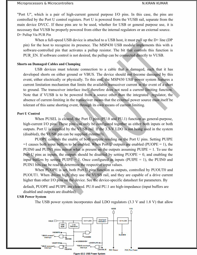
Microprocessors & Microcontrollers N.KIRAN KUMAR
"Port U", which is a pair of high-current general purpose I/O pins. In this case, the pins arecontrolled by the Port U control registers. Port U is powered from the VUSB rail, separate from themain device DVCC. If these pins are to be used, whether for USB or general purpose use, it isnecessary that VUSB be properly powered from either the internal regulators or an external source.D+ Pullup Via PUR Pin
When a full-speed USB device is attached to a USB host, it must pull up the D+ line (DPpin) for the host to recognize its presence. The MSP430 USB module implements this with asoftware-controlled pin that activates a pullup resistor. The bit that controls this function isPUR_EN. If software control is not desired, the pullup can be connected directly to VUSB.
Shorts on Damaged Cables and Clamping
USB devices must tolerate connection to a cable that is damaged, such that it hasdeveloped shorts on either ground or VBUS. The device should not become damaged by thisevent, either electrically or physically. To this end, the MSP430 USB power system features acurrent limitation mechanism that limits the available transceiver current in the event of a shortto ground. The transceiver interface itself therefore does not need a current limiting function.Note that if VUSB is to be powered from a source other than the integrated regulator, theabsence of current-limiting in the transceiver means that the external power source must itself betolerant of this same shorting event, through its own means of current limiting.
Port U Control
When PUSEL is cleared, the Port U pins (PU.0 and PU.1) function as general-purpose,high-current I/O pins. These pins can only be configured together as either both inputs or bothoutputs. Port U is supplied by the VUSB rail. If the 3.3-V LDO is not being used in the system(disabled), the VUSB pin can be supplied externally.
PUOPE controls the enable of both outputs residing on the Port U pins. Setting PUIPE=1 causes both input buffers to be enabled. When Port U outputs are enabled (PUOPE = 1), thePUIN0 and PUIN1 pins mirror what is present on the outputs assuming PUIPE = 1. To use thePort U pins as inputs, the outputs should be disabled by setting PUOPE = 0, and enabling theinput buffers by setting PUIPE = 1. Once configured as inputs (PUIPE = 1), the PUIN0 andPUIN1 bits can be read to determine the respective input values.
When PUOPE is set, both Port U pins function as outputs, controlled by PUOUT0 andPUOUT1. When driven high, they use the VUSB rail, and they are capable of a drive currenthigher than other I/O pins on the device. See the device-specific datasheet for parameters. By
default, PUOPE and PUIPE are cleared. PU.0 and PU.1 are high-impedance (input buffers are disabled and outputs are disabled).
USB Power System
The USB power system incorporates dual LDO regulators (3.3 V and 1.8 V) that allow
126

Microprocessors & Microcontrollers N.KIRAN KUMAR
the entire MSP430 device to be powered from 5-V VBUS when it is made available from theUSB host. Alternatively, the power system can supply power only to the USB module, or it canbe unused altogether, as in a fully selfpowered device. The block diagram is shown in Figure 42-2
The 3.3-V LDO receives 5 V from VBUS and provides power to the transceiver, as wellas the VUSB pin. Using this setup prevents the relatively high load of the transceiver and PLLfrom loading a local system power supply, if used. Thus it is very useful in battery-powereddevices.
The 1.8-V LDO receives power from the VUSB pin – which is to be sourced either fromthe internal 3.3-V LDO or externally – and provides power to the USB PLL and transceiver. The1.8-V LDO in the USB module is not related to the LDO that resides in the MSP430 PowerManagement Module (PMM). The inputs and outputs of the LDOs are shown in Figure 42-2.VBUS, VUSB, and V18 need to be connected to external capacitors. The V18 pin is notintended to source other components in the system, rather it exists solely for the attachment of aload capacitor.
Enabling and Disabling
The 3.3-V LDO is enabled or disabled by setting or clearing VUSBEN, respectively.Even if enabled, if the voltage on VBUS is detected to be low or nonexistent, the LDO issuspended. No additional current is consumed while the LDO is suspended. When VBUS risesabove the USB power brownout level, the LDO reference and low voltage detection becomeenabled. When VBUS rises further above the launch voltage VLAUNCH, the LDO modulebecomes enabled (see Figure 42-3). See device-specific data sheet for value of VLAUNCH.
The 1.8-V LDO can be enabled or disabled by setting SLDOEN accordingly. By default,the 1.8-V LDO is controlled automatically according to whether power is available on VBUS.This auto-enable feature is controlled by SLDOAON. In this case, that the SLDOEN bit doesnot reflect the state of the 1.8-V LDO. If the user wishes to know the state while using the auto-enable feature, the USBBGVBV bit inUSBPWRCTL can be read. In addition, to disable the 1.8-V LDO, SLDOAON must be clearedalong with SLDOEN. If providing VUSB from an external source, rather than through theintegrated 3.3-V LDO, keep in mind that if 5 V is not present on VBUS, the 1.8-V LDO is notautomatically enabled. In this situation, either VBUS much be attached to USB bus power, orthe SLDOAON bit must be cleared and SLDOEN set.
It is required that power from the USB cable's VBUS be directed through a Schottky
127
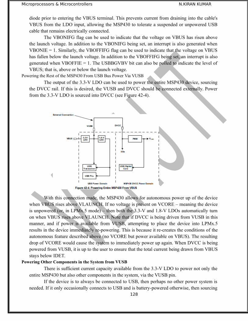
Microprocessors & Microcontrollers N.KIRAN KUMAR
diode prior to entering the VBUS terminal. This prevents current from draining into the cable'sVBUS from the LDO input, allowing the MSP430 to tolerate a suspended or unpowered USBcable that remains electrically connected.
The VBONIFG flag can be used to indicate that the voltage on VBUS has risen abovethe launch voltage. In addition to the VBONIFG being set, an interrupt is also generated whenVBONIE = 1. Similarly, the VBOFFIFG flag can be used to indicate that the voltage on VBUShas fallen below the launch voltage. In addition to the VBOFFIFG being set, an interrupt is alsogenerated when VBOFFIE = 1. The USBBGVBV bit can also be polled to indicate the level ofVBUS; that is, above or below the launch voltage.
Powering the Rest of the MSP430 From USB Bus Power Via VUSB
The output of the 3.3-V LDO can be used to power the entire MSP430 device, sourcingthe DVCC rail. If this is desired, the VUSB and DVCC should be connected externally. Powerfrom the 3.3-V LDO is sourced into DVCC (see Figure 42-4).
With this connection made, the MSP430 allows for autonomous power up of the devicewhen VBUS rises above VLAUNCH. If no voltage is present on VCORE – meaning the deviceis unpowered (or, in LPMx.5 mode) – then both the 3.3-V and 1.8-V LDOs automatically turnon when VBUS rises above VLAUNCH. Note that if DVCC is being driven from VUSB in thismanner, and if power is available from VUSB, attempting to place the device into LPMx.5results in the device immediately re-powering. This is because it re-creates the conditions of theautonomous feature described above (no VCORE but power available on VBUS). The resultingdrop of VCORE would cause the system to immediately power up again. When DVCC is beingpowered from VUSB, it is up to the user to ensure that the total current being drawn from VBUSstays below IDET.
Powering Other Components in the System from VUSB
There is sufficient current capacity available from the 3.3-V LDO to power not only theentire MSP430 but also other components in the system, via the VUSB pin.
If the device is to always be connected to USB, then perhaps no other power system isneeded. If it only occasionally connects to USB and is battery-powered otherwise, then sourcing
128

Microprocessors & Microcontrollers N.KIRAN KUMAR
system power via the 3.3-V LDO takes power burden away from the battery. Alternatively, if thebattery is rechargeable, the recharging can be driven from VUSB.
Self-Powered Devices
Some applications may be self-powered, in that the VUSB power is supplied externally.In these cases, the 3.3-V LDO would be disabled (VUSBEN = 0). For proper USB operation, thevoltage on VBUS can still be detected, even while the 3.3-V LDO disabled, by settingUSBDETEN = 1. When VBUS rises above the USB power brownout level, low voltagedetection becomes enabled. When VBUS rises further above the launch voltage VLAUNCH, thevoltage on VBUS is detected.
Current Limitation and Overload Protection
The 3.3-V LDO features current limitation to protect the transceiver during shorted-cableconditions. A short or overload condition – that is, when the output of the LDO becomescurrent-
129
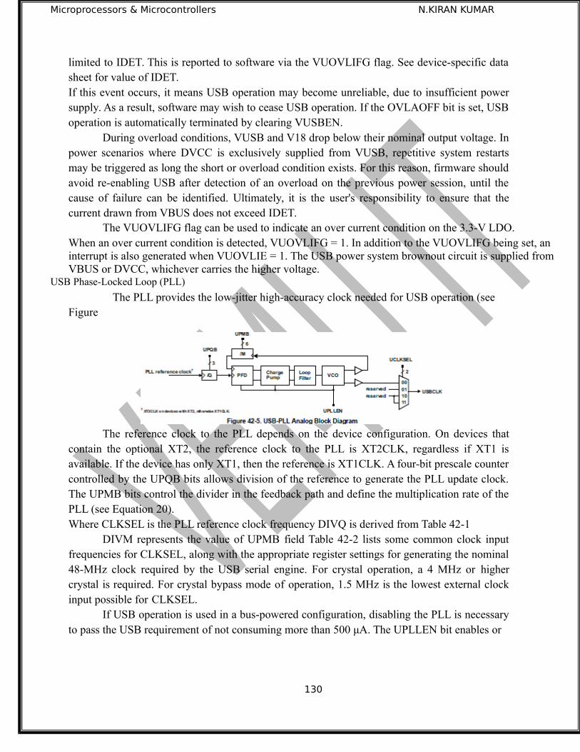
Microprocessors & Microcontrollers N.KIRAN KUMAR
limited to IDET. This is reported to software via the VUOVLIFG flag. See device-specific datasheet for value of IDET.If this event occurs, it means USB operation may become unreliable, due to insufficient powersupply. As a result, software may wish to cease USB operation. If the OVLAOFF bit is set, USBoperation is automatically terminated by clearing VUSBEN.
During overload conditions, VUSB and V18 drop below their nominal output voltage. Inpower scenarios where DVCC is exclusively supplied from VUSB, repetitive system restartsmay be triggered as long the short or overload condition exists. For this reason, firmware shouldavoid re-enabling USB after detection of an overload on the previous power session, until thecause of failure can be identified. Ultimately, it is the user's responsibility to ensure that thecurrent drawn from VBUS does not exceed IDET.
The VUOVLIFG flag can be used to indicate an over current condition on the 3.3-V LDO.When an over current condition is detected, VUOVLIFG = 1. In addition to the VUOVLIFG being set, an interrupt is also generated when VUOVLIE = 1. The USB power system brownout circuit is supplied from VBUS or DVCC, whichever carries the higher voltage.
USB Phase-Locked Loop (PLL)
The PLL provides the low-jitter high-accuracy clock needed for USB operation (seeFigure
The reference clock to the PLL depends on the device configuration. On devices thatcontain the optional XT2, the reference clock to the PLL is XT2CLK, regardless if XT1 isavailable. If the device has only XT1, then the reference is XT1CLK. A four-bit prescale countercontrolled by the UPQB bits allows division of the reference to generate the PLL update clock.The UPMB bits control the divider in the feedback path and define the multiplication rate of thePLL (see Equation 20).Where CLKSEL is the PLL reference clock frequency DIVQ is derived from Table 42-1
DIVM represents the value of UPMB field Table 42-2 lists some common clock inputfrequencies for CLKSEL, along with the appropriate register settings for generating the nominal48-MHz clock required by the USB serial engine. For crystal operation, a 4 MHz or highercrystal is required. For crystal bypass mode of operation, 1.5 MHz is the lowest external clockinput possible for CLKSEL.
If USB operation is used in a bus-powered configuration, disabling the PLL is necessaryto pass the USB requirement of not consuming more than 500 μA. The UPLLEN bit enables or
130
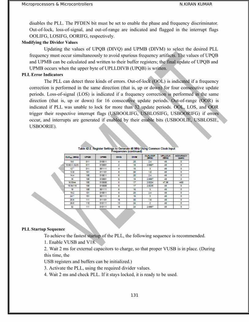
Microprocessors & Microcontrollers N.KIRAN KUMAR
disables the PLL. The PFDEN bit must be set to enable the phase and frequency discriminator.Out-of-lock, loss-of-signal, and out-of-range are indicated and flagged in the interrupt flagsOOLIFG, LOSIFG, OORIFG, respectively.
Modifying the Divider Values
Updating the values of UPQB (DIVQ) and UPMB (DIVM) to select the desired PLLfrequency must occur simultaneously to avoid spurious frequency artifacts. The values of UPQBand UPMB can be calculated and written to their buffer registers; the final update of UPQB andUPMB occurs when the upper byte of UPLLDIVB (UPQB) is written.
PLL Error Indicators
The PLL can detect three kinds of errors. Out-of-lock (OOL) is indicated if a frequencycorrection is performed in the same direction (that is, up or down) for four consecutive updateperiods. Loss-of-signal (LOS) is indicated if a frequency correction is performed in the samedirection (that is, up or down) for 16 consecutive update periods. Out-of-range (OOR) isindicated if PLL was unable to lock for more than 32 update periods. OOL, LOS, and OORtrigger their respective interrupt flags (USBOOLIFG, USBLOSIFG, USBOORIFG) if errorsoccur, and interrupts are generated if enabled by their enable bits (USBOOLIE, USBLOSIE,USBOORIE).
PLL Startup Sequence
To achieve the fastest startup of the PLL, the following sequence is recommended.1. Enable VUSB and V18.2. Wait 2 ms for external capacitors to charge, so that proper VUSB is in place. (During this time, theUSB registers and buffers can be initialized.)3. Activate the PLL, using the required divider values.4. Wait 2 ms and check PLL. If it stays locked, it is ready to be used.
131
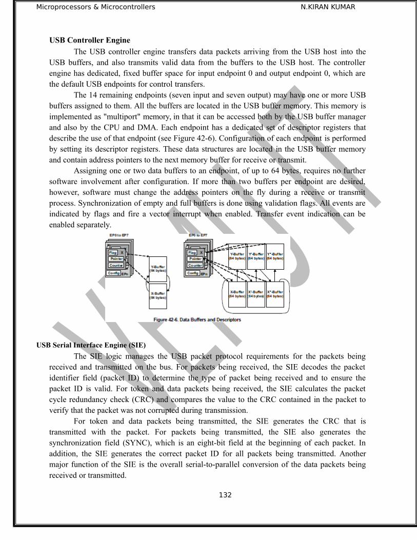
Microprocessors & Microcontrollers N.KIRAN KUMAR
USB Controller Engine
The USB controller engine transfers data packets arriving from the USB host into theUSB buffers, and also transmits valid data from the buffers to the USB host. The controllerengine has dedicated, fixed buffer space for input endpoint 0 and output endpoint 0, which arethe default USB endpoints for control transfers.
The 14 remaining endpoints (seven input and seven output) may have one or more USBbuffers assigned to them. All the buffers are located in the USB buffer memory. This memory isimplemented as "multiport" memory, in that it can be accessed both by the USB buffer managerand also by the CPU and DMA. Each endpoint has a dedicated set of descriptor registers thatdescribe the use of that endpoint (see Figure 42-6). Configuration of each endpoint is performedby setting its descriptor registers. These data structures are located in the USB buffer memoryand contain address pointers to the next memory buffer for receive or transmit.
Assigning one or two data buffers to an endpoint, of up to 64 bytes, requires no furthersoftware involvement after configuration. If more than two buffers per endpoint are desired,however, software must change the address pointers on the fly during a receive or transmitprocess. Synchronization of empty and full buffers is done using validation flags. All events areindicated by flags and fire a vector interrupt when enabled. Transfer event indication can beenabled separately.
USB Serial Interface Engine (SIE)
The SIE logic manages the USB packet protocol requirements for the packets beingreceived and transmitted on the bus. For packets being received, the SIE decodes the packetidentifier field (packet ID) to determine the type of packet being received and to ensure thepacket ID is valid. For token and data packets being received, the SIE calculates the packetcycle redundancy check (CRC) and compares the value to the CRC contained in the packet toverify that the packet was not corrupted during transmission.
For token and data packets being transmitted, the SIE generates the CRC that istransmitted with the packet. For packets being transmitted, the SIE also generates thesynchronization field (SYNC), which is an eight-bit field at the beginning of each packet. Inaddition, the SIE generates the correct packet ID for all packets being transmitted. Anothermajor function of the SIE is the overall serial-to-parallel conversion of the data packets beingreceived or transmitted.
132
Microprocessors & Microcontrollers N.KIRAN KUMAR
USB Buffer Manager (UBM)
The USB buffer manager provides the control logic that interfaces the SIE to the USBendpoint buffers. One of the major functions of the UBM is to decode the USB device addressto determine if the USB host is addressing this particular USB device. In addition, the endpointaddress field and direction signal are decoded to determine which particular USB endpoint isbeing addressed. Based on the direction of the USB transaction and the endpoint number, theUBM either writes or reads the data packet to or from the appropriate USB endpoint data buffer.
The TOGGLE bit for each output endpoint configuration register is used by the UBMto track successful output data transactions. If a valid data packet is received and the data packetID matches the expected packet ID, the TOGGLE bit is toggled. Similarly, the TOGGLE bit foreach input endpoint configuration is used by the UBM to track successful input datatransactions. If a valid data packet is transmitted, the TOGGLE bit is toggled. If the TOGGLEbit is cleared, a DATA0 packet ID is transmitted in the data packet to the host. If the TOGGLEbit is set, a DATA1 packet ID is transmitted in the data packet to the host. See Section 42.3regarding details of USB transfers.
USB Buffer Memory
The USB buffer memory contains the data buffers for all endpoints and for SETUPpackets. In that the buffers for endpoints 1 to 7 are flexible, there are USB buffer configurationregisters that define them, and these too are in the USB buffer memory. (Endpoint 0 is definedwith a set of registers in the USB control register space.) Storing these in open memory allowsfor efficient, flexible use, which is advantageous because use of these endpoints is veryapplication-specific.
This memory is implemented as "multiport" memory, in that it can be accessed both bythe USB buffer manager and also by the CPU and DMA. The SIE allows CPU or DMA access,but reserves priority. As a result, CPU or DMA access is delayed using wait states if a conflictarises with an SIE access. When the USB module is disabled (USBEN = 0), the buffer memorybehaves like regular RAM. When changing the state of the USBEN bit (enabling or disabling theUSB module), the USB buffer memory should not be accessed within four clocks before andeight clocks after changing this bit, as doing so reconfigures the access method to the USBmemory.Accessing of the USB buffer memory by CPU or DMA is only possible if the USB PLL isactive. When a host requests suspend condition the application software (for example, USBstack) of client has to switch off the PLL within 10 ms. Note that the MSP430 USB suspendinterrupt occurs around 5 ms after the host request.
Each endpoint is defined by a block of six configuration "registers" (based in RAM, theyare not true registers in the strict sense of the word). These registers specify the endpoint type,buffer address, buffer size and data packet byte count. They define an endpoint buffer space thatis 1904 bytes in size. An additional 24 bytes are allotted to three remaining blocks – the EP0_INbuffer, the EP0_OUT buffer, and the SETUP packet buffer (see Table 42-3).
133
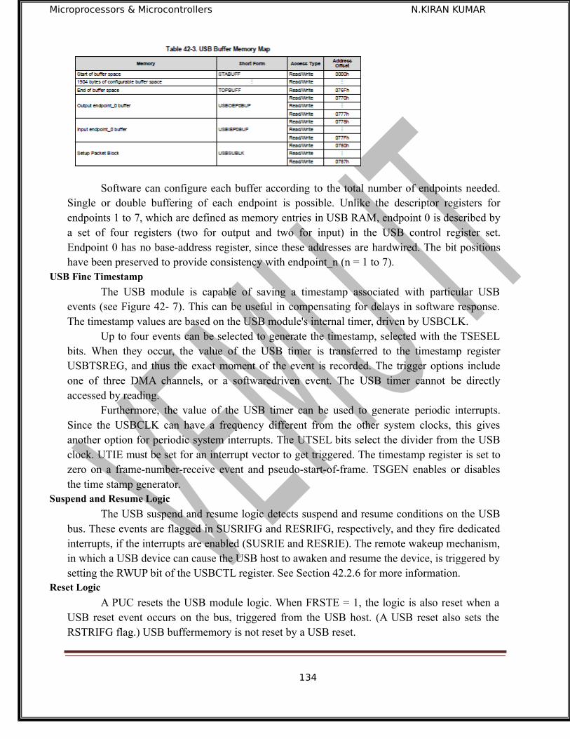
Microprocessors & Microcontrollers N.KIRAN KUMAR
Software can configure each buffer according to the total number of endpoints needed.Single or double buffering of each endpoint is possible. Unlike the descriptor registers forendpoints 1 to 7, which are defined as memory entries in USB RAM, endpoint 0 is described bya set of four registers (two for output and two for input) in the USB control register set.Endpoint 0 has no base-address register, since these addresses are hardwired. The bit positionshave been preserved to provide consistency with endpoint_n (n = 1 to 7).
USB Fine Timestamp
The USB module is capable of saving a timestamp associated with particular USBevents (see Figure 42- 7). This can be useful in compensating for delays in software response.The timestamp values are based on the USB module's internal timer, driven by USBCLK.
Up to four events can be selected to generate the timestamp, selected with the TSESELbits. When they occur, the value of the USB timer is transferred to the timestamp registerUSBTSREG, and thus the exact moment of the event is recorded. The trigger options includeone of three DMA channels, or a softwaredriven event. The USB timer cannot be directlyaccessed by reading.
Furthermore, the value of the USB timer can be used to generate periodic interrupts.Since the USBCLK can have a frequency different from the other system clocks, this givesanother option for periodic system interrupts. The UTSEL bits select the divider from the USBclock. UTIE must be set for an interrupt vector to get triggered. The timestamp register is set tozero on a frame-number-receive event and pseudo-start-of-frame. TSGEN enables or disablesthe time stamp generator.
Suspend and Resume Logic
The USB suspend and resume logic detects suspend and resume conditions on the USBbus. These events are flagged in SUSRIFG and RESRIFG, respectively, and they fire dedicatedinterrupts, if the interrupts are enabled (SUSRIE and RESRIE). The remote wakeup mechanism,in which a USB device can cause the USB host to awaken and resume the device, is triggered bysetting the RWUP bit of the USBCTL register. See Section 42.2.6 for more information.
Reset Logic
A PUC resets the USB module logic. When FRSTE = 1, the logic is also reset when aUSB reset event occurs on the bus, triggered from the USB host. (A USB reset also sets theRSTRIFG flag.) USB buffermemory is not reset by a USB reset.
134
MICROPROCESSORS & MICROCONTROLLERSN.KIRAN KUMAR M.Tech
USB Vector Interrupts
The USB module uses a single interrupt vector generator register tohandle multiple USB interrupts. All USB-related interrupt sources trigger theUSBVECINT (also called USBIV) vector, which then contains a 6-bit vectorvalue that identifies the interrupt source. Each of the interrupt sources results ina different offset value read. The interrupt vector returns zero when nointerrupt is pending.
Reading the interrupt vector register clears the corresponding interruptflag and updates its value. The interrupt with highest priority returns the value0002h; the interrupt with lowest priority returns the value 003Eh when readingthe interrupt vector register. Writing to this register clears all interrupt flags.For each input and output endpoints resides an USB transaction interruptindication enable. Software may set this bit to define if interrupts are to beflagged in general. To generate an interrupt the corresponding interrupt enableand flag must be set.Power Consumption
USB functionality consumes more power than is typically drawn in theMSP430. Since most MSP430applications are power sensitive, the MSP430USB module has been designed to protect the battery by ensuring thatsignificant power load only occurs when attached to the bus, allowing power tobe drawn from VBUS.
The two components of the USB module that draw the most current arethe transceiver and the PLL. The transceiver can consume large amounts ofpower while transmitting, but in its quiescent state – that is, when nottransmitting data – the transceiver actually consumes very little power. This isthe amount specified as IIDLE. This amount is so little that the transceiver canbe kept active during suspend mode without presenting a problem for bus-powered applications. Fortunately the transceiver always has access to VBUSpower when drawing the level of current required for transmitting.
The PLL consumes a larger amount of current. However, it need only beactive while connected to the host, and the host can supply the power. When thePLL is disabled (for example, during USB suspend), USBCLK automatically issourced from the VLO.
Suspend and Resume
All USB devices must support the ability to be suspended into a no-activity state, and later resumed. When suspended, a device is not allowed toconsume more than 500uA from the USB's VBUS power rail, if the device isdrawing any power from that source. A suspended device must also monitor fora resume event on the bus.
The host initiates a suspend condition by creating a constant idle stateon the bus for more than 3.0 ms. It is the responsibility of the software to ensurethe device enters its low power suspend state within 10 ms of the suspendcondition. The USB specification requires that a suspended bus-powered USB
135

MICROPROCESSORS & MICROCONTROLLERSN.KIRAN KUMAR M.Tech
device not draw in excess of 500 μA from the bus.Entering Suspend
When the host suspends the USB device, a suspend interrupt isgenerated (SUSRIFG). From this point, the software has 10 ms to ensure thatno more than 500uA is being drawn from the host via VBUS.For most applications, the integrated 3.3-V LDO is being used. In this case, thefollowing actions should be taken:
• Disable the PLL by clearing UPLLEN (UPLLEN = 0)• Limit all current sourced from VBUS that causes the total currentsourced from VBUS equal to 500 μA minus the suspend current,ISUSPEND (see the device-specific data sheet).Disabling the PLL eliminates the largest on-chip draw of power from
VBUS. During suspend, the USBCLK is automatically sourced by the VLO(VLOCLK), allowing the USB module to detect resume when it occurs. It is agood idea to also then ensure that the RESRIE bit is also set, so that aninterrupt is generated when the host resumes the device. If desired, the highfrequency crystal can also be disabled to save additional system power,however it does not contribute to the power from VBUS since it draws powerfrom the DVCC supply.
Entering Resume Mode
When the USB device is in a suspended condition, any non-idlesignaling, including reset signaling, on the host side is detected by the suspendand resume logic and device operation is resumed. RESRIFG is set, causing anUSB interrupt. The interrupt service routine can be used to resume USBoperation.
USB Transfers
The USB module supports control, bulk, and interrupt data transfertypes. In accordance with the USB specification, endpoint 0 is reserved for thecontrol endpoint and is bidirectional. In addition to the control endpoint, theUSB module is capable of supporting up to 7 input endpoints and 7 outputendpoints. These additional endpoints can be configured either as bulk orinterrupt endpoints. The software handles all control, bulk, and interruptendpoint transactions.
Control Transfers
Control transfers are used for configuration, command, and statuscommunication between the host and the USB device. Control transfers to theUSB device use input endpoint 0 and output endpoint 0. The three types ofcontrol transfers are control write, control write with no data stage, and controlread. Note that the control endpoint must be initialized before connecting theUSB device to the USB
Control Write Transfer
The host uses a control write transfer to write data to the USB device. Acontrol write transfer consists of a setup stage transaction, at least one outputdata stage transaction, and an input status stage transaction. The stagetransactions for a control write transfer are:
136
MICROPROCESSORS & MICROCONTROLLERSN.KIRAN KUMAR M.Tech
• Setup stage transaction:1. Input endpoint 0 and output endpoint 0 are initialized byprogramming the appropriate USB endpoint configuration blocks. Thisentails enabling the endpoint interrupt (USBIIE= 1) and enabling the endpoint (UBME = 1). The NAK bit for bothinput endpoint 0 and output endpoint 0 must be cleared.2. The host sends a setup token packet followed by the setup datapacket addressed to output endpoint 0. If the data is received without anerror, then the UBM writes the data
to the setup data packet buffer, sets the setup stage transaction bit(SETUPIFG = 1) in the USB Interrupt Flag register (USBIFG), returnsan ACK handshake to the host, and asserts the setup stage transactioninterrupt. Note that as long as SETUPIFG = 1, the UBM returns a NAKhandshake for any data stage or status stage transactions regardless ofthe endpoint 0 NAK or STALL bit values.3. The software services the interrupt, reads the setup data packet fromthe buffer, and then decodes the command. If the command is notsupported or invalid, the software should set the STALL bit in the outputendpoint 0 configuration register (USBOEPCNFG_0) and the inputendpoint 0 configuration register (USBIEPCNFG_0) . This causes thedevice to return a STALL handshake for any data or status stagetransaction. For control write transfers, the packet ID used by the hostfor the first data packet output is a DATA1 packet ID and the TOGGLEbit must match.
NOTE: When using USBIV, SETUPIFG is cleared upon reading USBIV. Inaddition, the NAK onb input endpoint 0 and output endpoint 0 are also cleared.In this case, the host may send or receive the next setup packet even if MSP430did not perform the first setup packet. To prevent this, first read the SETUPIFGdirectly, perform the required setup, and then use the USBIV for furtherprocessing.NOTE: The priority of input endpoint 0 is higher than the setup flag insideUSBIV (SETUPIFG). Therefore, if both the USBIEPIFG.EP0 and SETUPIFGare pending, reading USBIV gives the higher priority interrupt (EP0) asopposed to SETUPIFG. Therefore, read SETUPIFG directly, process thepending setup packet, then proceed to read the USBIV.• Data stage transaction:
1. The host sends an OUT token packet followed by a data packetaddressed to output endpoint 0. If the data is received without an error,the UBM writes the data to the output endpoint buffer(USBOEP0BUF), updates the data count value, toggles the TOGGLEbit, sets the NAK bit, returns an ACK handshake to the host , andasserts the output endpoint interrupt 0 (OEPIFG0).2. The software services the interrupt and reads the data packet from theoutput endpoint buffer. To read the data packet, the software first needsto obtain the data count value inside theUSBOEPBCNT_0 register. After reading the data packet, the softwareshould clear the NAK bit to allow the reception of the next data packetfrom the host.3. If the NAK bit is set when the data packet is received, the UBMsimply returns a NAK handshake to the host. If the STALL bit is setwhen the data packet is received, the UBM simply returns a STALL
137
MICROPROCESSORS & MICROCONTROLLERSN.KIRAN KUMAR M.Tech
handshake to the host. If a CRC or bit stuff error occurs when the datapacket is received, then no handshake is returned to the host.
• Status stage transaction:1. For input endpoint 0, the software updates the data count value tozero, sets the TOGGLE bit, then clears the NAK bit to enable the datapacket to be sent to the host. Note that for a status stage transaction, anull data packet with a DATA1 packet ID is sent to the host.2. The host sends an IN token packet addressed to input endpoint 0.After receiving the IN token, the UBM transmits a null data packet tothe host. If the data packet is received without errors by the host, thenan ACK handshake is returned. The UBM then toggles the TOGGLE bitand sets the NAK bit.
3. If the NAK bit is set when the IN token packet is received, the UBMsimply returns a NAK handshake to the host. If the STALL bit is setwhen the IN token packet is received, the UBM simply returns aSTALL handshake to the host. If no handshake packet is received fromthe host, then the UBM prepares to retransmit the same data packetagain.
Control Write Transfer with No Data Stage Transfer
The host uses a control write transfer to write data to the USB device. Acontrol write with no data stage transfer consists of a setup stage transactionand an input status stage transaction. For this type of transfer, the data to bewritten to the USB device is contained in the two byte value field of the setupstage transaction data packet.The stage transactions for a control write transfer with no data stage transfer are:• Setup stage transaction:
1. Input endpoint 0 and output endpoint 0 are initialized byprogramming the appropriate USB endpoint configuration blocks. Thisentails programming the buffer size and buffer base address,selecting the buffer mode, enabling the endpoint interrupt (USBIIE = 1),initializing the TOGGLE bit, enabling the endpoint (UBME = 1). TheNAK bit for both input endpoint 0 and output endpoint 0 must becleared.2. The host sends a setup token packet followed by the setup data packetaddressed to output endpoint 0. If the data is received without an errorthen the UBM writes the data to the setup data packet buffer, sets thesetup stage transaction (SETUP) bit in the USB status register, returnsanACK handshake to the host, and asserts the setup stage transactioninterrupt. Note that as long as the setup transaction (SETUP) bit is set,the UBM returns a NAK handshake for any data stage or status stagetransaction regardless of the endpoint 0 NAK or STALL bit values.3. The software services the interrupt and reads the setup data packetfrom the buffer then decodes the command. If the command is notsupported or invalid, the software should set the STALL bits in theoutput endpoint 0 and the input endpoint 0 configuration registersbefore clearing the setup stage transaction (SETUP) bit. This causes thedevice to return a STALL handshake for data or status stagetransactions. After reading the data packet and decoding the command,the software should clear the interrupt, which automatically clears the
138
MICROPROCESSORS & MICROCONTROLLERSN.KIRAN KUMAR M.Tech
setup stage transaction status bit.NOTE: When using USBIV, the SETUPIFG is cleared upon reading USBIV. Inaddition, the NAK o input endpoint 0 and output endpoint 0 is also cleared. Inthis case, the host may send or receive the next setup packet even if MSP430did not perform the first setup packet. To prevent this, first read the SETUPIFGdirectly, perform the required setup, and then use the USBIV for furtherprocessing.NOTE: The priority of input endpoint 0 is higher than setup flag inside USBIV.Therefore, if both the USBIEPIFG.EP0 and SETUPIFG are pending, readingthe USBIV gives the higher priority interrupt (EP0) as opposed to theSETUPIFG. Therefore, read SETUPIFG directly, process the pending setuppacket, then proceed to read the USBIV.• Status stage transaction:
1. For input endpoint 0, the software updates the data count value tozero, sets the TOGGLE bit then clears the NAK bit to enable the datapacket to be sent to the host. Note that for a status stage transaction anull data packet with a DATA1 packet ID is sent to the host.
2. The host sends an IN token packet addressed to input endpoint 0.After receiving the IN token, theUBM transmits a null data packet to the host. If the data packet isreceived without errors by the host, then an ACK handshake is returned.The UBM then toggles the TOGGLE bit, sets the NAK bit, and assertsthe endpoint interrupt.3. If the NAK bit is set when the IN token packet is received, the UBMsimply returns a NAK handshake to the host. If the STALL bit is setwhen the IN token packet is received, the UBM simply returns aSTALL handshake to the host. If no handshake packet is received fromthe host, then the UBM prepares to retransmit the same data packetagain.
Control Read Transfer
The host uses a control read transfer to read data from the USB device.A control read transfer consists of a setup stage transaction, at least one inputdata stage transaction and an output status stage transaction. The stagetransactions for a control read transfer are:• Setup stage transaction:
1. Input endpoint 0 and output endpoint 0 are initialized byprogramming the appropriate USB endpoint configuration blocks. Thisentails enabling the endpoint interrupt (USBIIE= 1) and enabling the endpoint (UBME = 1). The NAK bit for bothinput endpoint 0 and output endpoint 0 must be cleared.2. The host sends a setup token packet followed by the setup data packetaddressed to output endpoint 0. If the data is received without an error,then the UBM writes the data to the setup buffer, sets the setup stagetransaction (SETUP) bit in the USB status register, returns an ACKhandshake to the host, and asserts the setup stage transaction interrupt.Note that as long as the setup transaction (SETUP) bit is set, the UBMreturns a NAK handshake for any data stage or status stage transactionsregardless of the endpoint 0 NAK or STALL bit values.3. The software services the interrupt and reads the setup data packetfrom the buffer then decodes the command. If the command is notsupported or invalid, the software should set the STALL bits in the
139

MICROPROCESSORS & MICROCONTROLLERSN.KIRAN KUMAR M.Tech
output endpoint 0 and the input endpoint 0 configuration registersbefore clearing the setup stage transaction (SETUP) bit. This causes thedevice to return a STALL handshake for a data stage or status stagetransactions. After reading the data packet and decoding the command,the software should clear the interrupt, which automatically clears thesetup stage transaction status bit. The software should also set theTOGGLE bit in the input endpoint 0 configuration register. For controlread transfers, the packet ID used by the host for the first input datapacket is a DATA1 packet ID.
NOTE: When using USBIV, the SETUPIFG is cleared upon reading USBIV. Inaddition, it also the clears NAK on input endpoint 0 and output endpoint 0. Inthis case, the host may send or receive the next setup packet even if MSP430did not perform the first setup packet. To prevent this, first read the SETUPIFGdirectly, perform the required setup, and then use the USBIV for furtherprocessing.NOTE: The priority of input endpoint 0 is higher than the setup flag insideUSBIV. Therefore, if both the USBIEPIFG.EP0 and SETUPIFG are pending,reading the USBIV gives the higher priority interrupt (EP0) as opposed to theSETUPIFG. Therefore, read SETUPIFG directly, process the pending setuppacket, then proceed to read the USBIV.• Data stage transaction:
1. The data packet to be sent to the host is written to the input endpoint0 buffer by the software. The software also updates the data count valuethen clears the input endpoint 0 NAK bit to enable the data packet to besent to the host.2. The host sends an IN token packet addressed to input endpoint 0.After receiving the IN token, the UBM transmits the data packet to thehost. If the data packet is received without errors by the host, then anACK handshake is returned. The UBM sets the NAK bit and asserts theendpoint interrupt.3. The software services the interrupt and prepares to send the next datapacket to the host.4. If the NAK bit is set when the IN token packet is received, the UBMsimply returns a NAK handshake to the host. If the STALL bit is setwhen the IN token packet is received, the UBM simply returns aSTALL handshake to the host. If no handshake packet is received fromthe host, then the UBM prepares to retransmit the same data packetagain.5. The software continues to send data packets until all data has been sent to the host.
• Status stage transaction:1. For output endpoint 0, the software sets the TOGGLE bit, then clearsthe NAK bit to enable the data packet to be sent to the host. Note thatfor a status stage transaction a null data packet with a DATA1 packet IDis sent to the host.2. The host sends an OUT token packet addressed to output endpoint 0.If the data packet is received Transfers without an error then the UBMupdates the data count value, toggles the TOGGLE bit, sets the NAKbit, returns an ACK handshake to the host, and asserts the endpointinterrupt.3. The software services the interrupt. If the status stage transactioncompleted successfully, then the software should clear the interrupt and
140
MICROPROCESSORS & MICROCONTROLLERSN.KIRAN KUMAR M.Tech
clear the NAK bit.4. If the NAK bit is set when the input data packet is received, the UBMsimply returns a NAK handshake to the host. If the STALL bit is setwhen the in data packet is received, the UBM simply returns a STALLhandshake to the host. If a CRC or bit stuff error occurs when the datapacket is received, then no handshake is returned to the host.
Interrupt Transfers
The USB module supports interrupt data transfers both to and from thehost. Devices that need to send or receive a small amount of data with aspecified service period are best served by the interrupt transfer type. Inputendpoints 1 through 7 and output endpoints 1 through 7 can be configured asinterrupt endpoints.
Interrupt OUT Transfer
The steps for an interrupt OUT transfer are:1. The software initializes one of the output endpoints as an outputinterrupt endpoint by programming the appropriate endpointconfiguration block. This entails programming the buffer size and bufferbase address, selecting the buffer mode, enabling the endpoint interrupt,initializing the toggle bit, enabling the endpoint, and clearing the NAKbit.2. The host sends an OUT token packet followed by a data packetaddressed to the output endpoint. If the data is received without an errorthen the UBM writes the data to the endpoint buffer, updates the datacount value, toggles the toggle bit, sets the NAK bit, returns an ACKhandshake to the host, and asserts the endpoint interrupt.3. The software services the interrupt and reads the data packet from thebuffer. To read the data packet, the software first needs to obtain thedata count value. After reading the
data packet, the software should clear the interrupt and clear the NAKbit to allow the reception of the next data packet from the host.4. If the NAK bit is set when the data packet is received, the UBMsimply returns a NAK handshake to the host. If the STALL bit is setwhen the data packet is received, the UBM simply returns a STALLhandshake to the host. If a CRC or bit stuff error occurs when the datapacket is received, then no handshake is returned to the host device.
In double buffer mode, the UBM selects between the X and Ybuffer based on the value of the toggle bit. If the toggle bit is a 0, theUBM writes the data packet to the X buffer. If the toggle bit is a 1, theUBM writes the data packet to the Y buffer. When a data packet isreceived, the software could determine which buffer contains the datapacket by reading the toggle bit. However, when using double buffermode, the possibility exists for data packets to be received and writtento both the X and Y buffer before the software responds to the endpointinterrupt. In this case, simply using the toggle bit to determine whichbuffer contains the data packet would not work. Hence, in double buffermode, the software should read the X buffer NAK bit, the Y buffer NAKbit, and the toggle bits to determine the status of the buffers.
Interrupt IN Transfer
The steps for an interrupt IN transfer are:1. The software initializes one of the input endpoints as an input
141
MICROPROCESSORS & MICROCONTROLLERSN.KIRAN KUMAR M.Tech
interrupt endpoint by programming the appropriate endpointconfiguration block. This entails programming the buffer size and bufferbase address, selecting the buffer mode, enabling the endpoint interrupt,initializing the toggle bit, enabling the endpoint, and setting the NAKbit.2. The data packet to be sent to the host is written to the buffer by thesoftware. The software also updates the data count value then clears theNAK bit to enable the data packet to be sent to the host.3. The host sends an IN token packet addressed to the input endpoint.After receiving the IN token, the UBM transmits the data packet to thehost. If the data packet is received without errors by the host, then anACK handshake is returned. The UBM then toggles the toggle bit, setsthe NAK bit, and asserts the endpoint interrupt.4. The software services the interrupt and prepares to send the next datapacket to the host.5. If the NAK bit is set when the in token packet is received, the UBMsimply returns a NAK handshake to the host. If the STALL bit is setwhen the IN token packet is received, the UBM simply returns a STALLhandshake to the host. If no handshake packet is received from the host,then the UBM prepares to retransmit the same data packet again. Indouble buffer mode, the UBM selects between the X and Y buffer basedon the value of the toggle bit. If the toggle bit is a 0, the UBM reads thedata packet from the X buffer. If the toggle bit is a 1, the UBM reads thedata packet from the Y buffer.
Bulk Transfers
The USB module supports bulk data transfers both to and from the host.Devices that need to send or receive a large amount of data without a suitablebandwidth are best served by the bulk transfer type. In endpoints 1 through 7and out endpoints 1 through 7 can all be configured as bulk endpoints.
Bulk OUT Transfer
The steps for a bulk OUT transfer are:
1. The software initializes one of the output endpoints as an output bulkendpoint by programming the appropriate endpoint configuration block.This entails programming the buffer size and buffer base address,selecting the buffer mode, enabling the endpoint interrupt, initializingthe toggle bit, enabling the endpoint, and clearing the NAK bit.2. The host sends an out token packet followed by a data packetaddressed to the output endpoint. If the data is received without an errorthen the UBM writes the data to the endpoint buffer, updates the datacount value, toggles the toggle bit, sets the NAK bit, returns an ACKhandshake to the host, an asserts the endpoint interrupt.3. The software services the interrupt and reads the data packet from thebuffer. To read the data packet, the software first needs to obtain the datacount value. After reading the data packet, the software should clear theinterrupt and clear the NAK bit to allow the reception of the next datapacket from the host.4. If the NAK bit is set when the data packet is received, the UBMsimply returns a NAK handshake to the host. If the STALL bit is setwhen the data packet is received, the UBM simply returns a STALLhandshake to the host. If a CRC or bit stuff error occurs when the data
142
MICROPROCESSORS & MICROCONTROLLERSN.KIRAN KUMAR M.Tech
packet is received, then no handshake is returned to the host.In double buffer mode, the UBM selects between the X and Y bufferbased on the value of the toggle bit. If the toggle bit is a 0, the UBMwrites the data packet to the X buffer. If the toggle bit is a 1, the UBMwrites the data packet to the Y buffer. When a data packet is received,the software could determine which buffer contains the data packet byreading the toggle bit. However, when using double buffer mode, thepossibility exists for data packets to be received and written to both theX and Y buffer before the software responds to the endpoint interrupt.In this case, simply using the toggle bit to determine which buffercontains the data packet would not work. Hence, in double buffer mode,the software should read the X buffer NAK bit, the Y buffer NAK bit,and the toggle bits to determine the status of the buffers.
Bulk IN Transfer
The steps for a bulk IN transfer are:1. The software initializes one of the input endpoints as an input bulkendpoint by programming the appropriate endpoint configuration block.This entails programming the buffer size and buffer base address,selecting the buffer mode, enabling the endpoint interrupt, initializingthe toggle bit, enabling the endpoint, and setting the NAK bit.2. The data packet to be sent to the host is written to the buffer by thesoftware. The software also updates the data count value then clears theNAK bit to enable the data packet to be sent to the host.3. The host sends an IN token packet addressed to the input endpoint.After receiving the IN token, the UBM transmits the data packet to thehost. If the data packet is received without errors by the host, then anACK handshake is returned. The UBM then toggles the toggle bit, setsthe NAK bit, and asserts the endpoint interrupt.4. The software services the interrupt and prepares to send the next datapacket to the host.5. If the NAK bit is set when the in token packet is received, the UBMsimply returns a NAK handshake to the host. If the STALL bit is setwhen the In token packet is received, the UBM simply returns a STALLhandshake to the host. If no handshake packet is received from the host,then the UBM prepares to retransmit the same data packet again. Indouble buffer mode , the UBM selects between the X and Y bufferbased on the value
of the toggle bit. If the toggle bit is a 0, the UBM reads the data packetfrom the X buffer. If the toggle bit is a 1, the UBM reads the data packetfrom the Y buffer.
Universal Serial Communication Interface (USCI): SPI mode
The universal serial communication interface (USCI) modules supportmultiple serial communication modes. Different USCI modules supportdifferent modes. Each different USCI module is named with a different letter.For example, USCI_A is different from USCI_B. If more than one identicalUSCI module is implemented on one device, those modules are named withincrementing numbers. For example, if one device has two USCI_A modules,they are named USCI_A0 and USCI_A1. See the device-specific data sheet todetermine which USCI modules, if any, are implemented on which devices.USCI_Ax modules support:
143
MICROPROCESSORS & MICROCONTROLLERSN.KIRAN KUMAR M.Tech
• UART mode• Pulse shaping for IrDA communications• Automatic baud-rate detection for LIN communications• S
PI modeUSCI_Bxmodulessupport:
• I2C mode• SPI mode
USCI Introduction – SPI Mode
In synchronous mode, the USCI connects the device to an externalsystem via three or four pins:UCxSIMO, UCxSOMI, UCxCLK, and UCxSTE. SPI mode is selected whenthe UCSYNC bit is set, andSPI mode (3-pin or 4-pin) is selected with theUCMODEx bits. SPI mode features include:
• 7-bit or 8-bit data length• LSB-first or MSB-first data transmit and receive• 3-pin and 4-pin SPI operation• Master or slave modes• Independent transmit and receive shift registers• Separate transmit and receive buffer registers• Continuous transmit and receive operation• Selectable clock polarity and phase control• Programmable clock frequency in master mode• Independent interrupt capability for receive and transmit• Slave operation in LPM4
USCI Operation – SPI Mode
In SPI mode, serial data is transmitted and received by multiple devicesusing a shared clock provided by the master. An additional pin, UCxSTE, isprovided to enable a device to receive and transmit data and is controlled by themaster.Three or four signals are used for SPI data exchange:
• UCxSIMO – slave in, master outMaster mode: UCxSIMO is thedata output line. Slave mode:UCxSIMO is the data input line.• UCxSOMI – slave out, master in
Master mode: UCxSOMI isthe data input line. Slavemode: UCxSOMI is the dataoutput line.• UCxCLK – USCISPI clock Mastermode: UCxCLK isan output. Slavemode: UCxCLK isan input.• UCxSTE – slave transmit enable
144

MICROPROCESSORS & MICROCONTROLLERSN.KIRAN KUMAR M.Tech
Used in 4-pin mode to allow multiple masters on a single bus. Not used in 3-pin mode.USCI Initialization and Reset
The USCI is reset by a PUC or by the UCSWRST bit. After a PUC, theUCSWRST bit is automatically set, keeping the USCI in a reset condition.When set, the UCSWRST bit resets the UCRXIE, UCTXIE, UCRXIFG,UCOE, and UCFE bits, and sets the UCTXIFG flag. Clearing UCSWRSTreleases the USCI for operation.
Character Format
The USCI module in SPI mode supports 7-bit and 8-bit characterlengths selected by the UC7BIT bit. In 7- bit data mode, UCxRXBUF is LSBjustified and the MSB is always reset. The UCMSB bit controls the direction ofthe transfer and selects LSB or MSB first.
Master Mode
shows the USCI as a master in both 3-pin and 4-pin configurations. TheUSCI initiates data transfer when data is moved to the transmit data bufferUCxTXBUF. The UCxTXBUF data is moved to thetransmit (TX) shift register when the TX shift register is empty, initiating datatransfer on UCxSIMO starting with either the MSB or LSB, depending on theUCMSB setting. Data on UCxSOMI is shifted into the receive shift register onthe opposite clock edge. When the character is received, the receive data ismoved from the receive (RX) shift register to the received data bufferUCxRXBUF and the receive interrupt flag UCRXIFG is set, indicating theRX/TX operation is complete.
A set transmit interrupt flag, UCTXIFG, indicates that data has movedfrom UCxTXBUF to the TX shift register and UCxTXBUF is ready for newdata. It does not indicate RX/TX completion. To receive data into the USCI inmaster mode, data must be written to UCxTXBUF, because receive andtransmit operations operate concurrently.
Pin SPI Master Mode
In 4-pin master mode, UCxSTE is used to prevent conflicts withanother master and controls the master as described in Table 37-1. WhenUCxSTE is in the master-inactive state:
• UCxSIMO and UCxCLK are set to inputs and no longer drive the bus.• The error bit UCFE is set, indicating a communication integrity
145
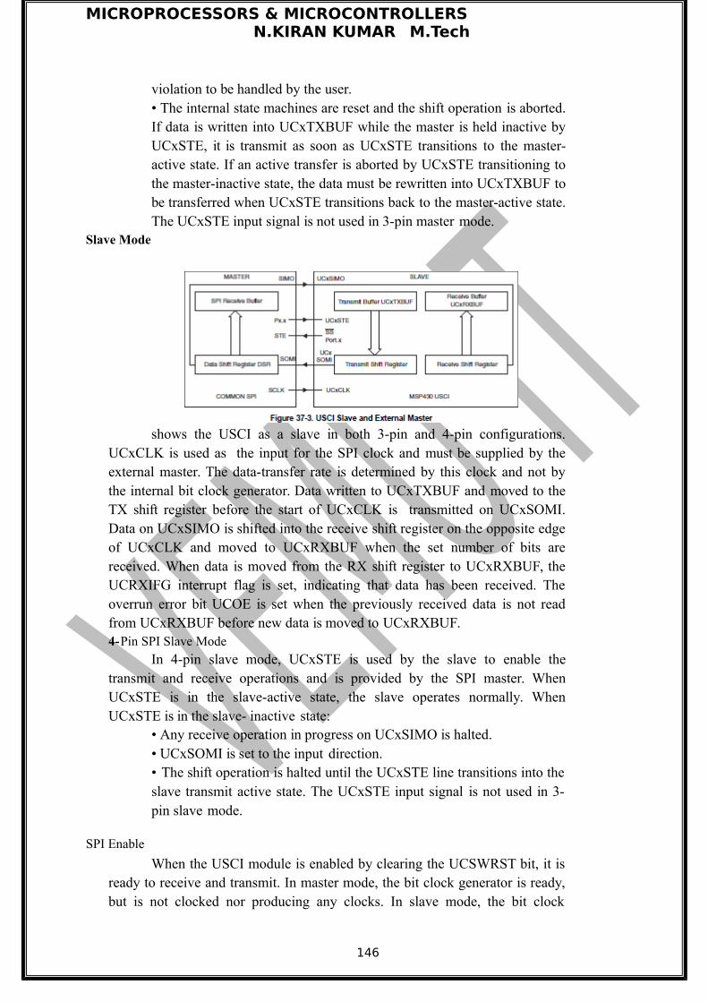
MICROPROCESSORS & MICROCONTROLLERSN.KIRAN KUMAR M.Tech
violation to be handled by the user.• The internal state machines are reset and the shift operation is aborted.If data is written into UCxTXBUF while the master is held inactive byUCxSTE, it is transmit as soon as UCxSTE transitions to the master-active state. If an active transfer is aborted by UCxSTE transitioning tothe master-inactive state, the data must be rewritten into UCxTXBUF tobe transferred when UCxSTE transitions back to the master-active state.The UCxSTE input signal is not used in 3-pin master mode.
Slave Mode
shows the USCI as a slave in both 3-pin and 4-pin configurations.UCxCLK is used as the input for the SPI clock and must be supplied by theexternal master. The data-transfer rate is determined by this clock and not bythe internal bit clock generator. Data written to UCxTXBUF and moved to theTX shift register before the start of UCxCLK is transmitted on UCxSOMI.Data on UCxSIMO is shifted into the receive shift register on the opposite edgeof UCxCLK and moved to UCxRXBUF when the set number of bits arereceived. When data is moved from the RX shift register to UCxRXBUF, theUCRXIFG interrupt flag is set, indicating that data has been received. Theoverrun error bit UCOE is set when the previously received data is not readfrom UCxRXBUF before new data is moved to UCxRXBUF.4-Pin SPI Slave Mode
In 4-pin slave mode, UCxSTE is used by the slave to enable thetransmit and receive operations and is provided by the SPI master. WhenUCxSTE is in the slave-active state, the slave operates normally. WhenUCxSTE is in the slave- inactive state:
• Any receive operation in progress on UCxSIMO is halted.• UCxSOMI is set to the input direction.• The shift operation is halted until the UCxSTE line transitions into theslave transmit active state. The UCxSTE input signal is not used in 3-pin slave mode.
SPI Enable
When the USCI module is enabled by clearing the UCSWRST bit, it isready to receive and transmit. In master mode, the bit clock generator is ready,but is not clocked nor producing any clocks. In slave mode, the bit clock
146
MICROPROCESSORS & MICROCONTROLLERSN.KIRAN KUMAR M.Tech
generator is disabled and the clock is provided by the
master. A transmit or receive operation is indicated by UCBUSY = 1. A PUC orset UCSWRST bit disables the USCI immediately and any active transfer isterminated.
Transmit Enable
In master mode, writing to UCxTXBUF activates the bit clockgenerator, and the data begins to transmit. In slave mode, transmission beginswhen a master provides a clock and, in 4- pin mode, when the UCxSTE is inthe slave-active state.
Receive Enable
The SPI receives data when a transmission is active. Receive andtransmit operations operate concurrently.
Serial Clock Control
UCxCLK is provided by the master on the SPI bus. When UCMST = 1,the bit clock is provided by the USCI bit clock generator on the UCxCLK pin.The clock used to generate the bit clock is selected with the UCSSELx bits.When UCMST = 0, the USCI clock is provided on the UCxCLK pin by themaster, the bit clock generator is not used, and the UCSSELx bits are don'tcare. The SPI receiver and transmitter operate in parallel and use the sameclock source for data transfer.
The 16-bit value of UCBRx in the bit rate control registers (UCxxBR1and UCxxBR0) is the division factor of the USCI clock source, BRCLK. Themaximum bit clock that can be generated in master mode is BRCLK.Modulation is not used in SPI mode, and UCAxMCTL should be cleared whenusing SPI mode for USCI_A. The UCAxCLK/UCBxCLK frequency is givenby:
fBitClock =fBRCLK / UCBRx IfUCBRx = 0,fBitClock = fBRCLKEven UCBRx settings result in even divisions and, thus, generate a bit clockwith a 50/50 duty cycle.Odd UCBRx settings result in odd divisions. In this case, the high phase of thebit clock is one BRCLK cycle longer than the low phase. When UCBRx = 0, nodivision is applied to BRCLK, and the bit clock equals BRCLK.
Serial Clock Polarity and Phase
The polarity and phase of UCxCLK are independently configured viathe UCCKPL and UCCKPH control bits of the USCI. Timing for each case isshown in Figure
Using the SPI Mode With Low-Power Modes
The USCI module provides automatic clock activation for use with low-power modes. When the USCI clock source is inactive because the device is ina low-power mode, the USCI module automatically activates it when needed,
147
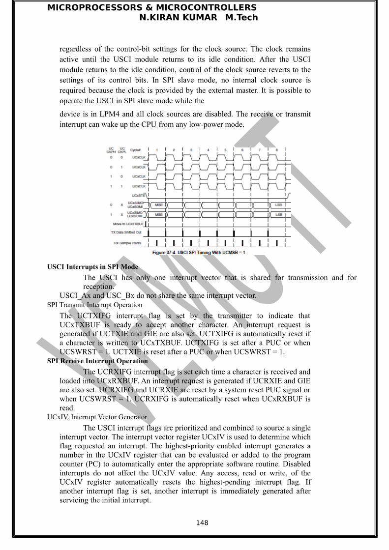
MICROPROCESSORS & MICROCONTROLLERSN.KIRAN KUMAR M.Tech
regardless of the control-bit settings for the clock source. The clock remainsactive until the USCI module returns to its idle condition. After the USCImodule returns to the idle condition, control of the clock source reverts to thesettings of its control bits. In SPI slave mode, no internal clock source isrequired because the clock is provided by the external master. It is possible tooperate the USCI in SPI slave mode while the
device is in LPM4 and all clock sources are disabled. The receive or transmitinterrupt can wake up the CPU from any low-power mode.
USCI Interrupts in SPI Mode
The USCI has only one interrupt vector that is shared for transmission and forreception.
USCI_Ax and USC_Bx do not share the same interrupt vector.SPI Transmit Interrupt Operation
The UCTXIFG interrupt flag is set by the transmitter to indicate thatUCxTXBUF is ready to accept another character. An interrupt request isgenerated if UCTXIE and GIE are also set. UCTXIFG is automatically reset ifa character is written to UCxTXBUF. UCTXIFG is set after a PUC or whenUCSWRST = 1. UCTXIE is reset after a PUC or when UCSWRST = 1.
SPI Receive Interrupt Operation
The UCRXIFG interrupt flag is set each time a character is received andloaded into UCxRXBUF. An interrupt request is generated if UCRXIE and GIEare also set. UCRXIFG and UCRXIE are reset by a system reset PUC signal orwhen UCSWRST = 1. UCRXIFG is automatically reset when UCxRXBUF isread.
UCxIV, Interrupt Vector Generator
The USCI interrupt flags are prioritized and combined to source a singleinterrupt vector. The interrupt vector register UCxIV is used to determine whichflag requested an interrupt. The highest-priority enabled interrupt generates anumber in the UCxIV register that can be evaluated or added to the programcounter (PC) to automatically enter the appropriate software routine. Disabledinterrupts do not affect the UCxIV value. Any access, read or write, of theUCxIV register automatically resets the highest-pending interrupt flag. Ifanother interrupt flag is set, another interrupt is immediately generated afterservicing the initial interrupt.
148
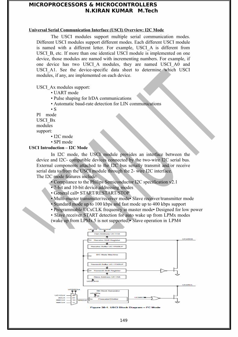
MICROPROCESSORS & MICROCONTROLLERSN.KIRAN KUMAR M.Tech
Universal Serial Communication Interface (USCI) Overview: I2C Mode
The USCI modules support multiple serial communication modes.Different USCI modules support different modes. Each different USCI moduleis named with a different letter. For example, USCI_A is different fromUSCI_B, etc. If more than one identical USCI module is implemented on onedevice, those modules are named with incrementing numbers. For example, ifone device has two USCI_A modules, they are named USCI_A0 andUSCI_A1. See the device-specific data sheet to determine which USCImodules, if any, are implemented on each device.
USCI_Ax modules support:• UART mode• Pulse shaping for IrDA communications• Automatic baud-rate detection for LIN communications• S
PI modeUSCI_Bxmodulessupport:
• I2C mode• SPI mode
USCI Introduction – I2C Mode
In I2C mode, the USCI module provides an interface between thedevice and I2C- compatible devices connected by the two-wire I2C serial bus.External components attached to the I2C bus serially transmit and/or receiveserial data to/from the USCI module through the 2- wire I2C interface.The I2C mode features include:
• Compliance to the Philips Semiconductor I2C specification v2.1• 7-bit and 10-bit device addressing modes• General call• START/RESTART/STOP• Multi-master transmitter/receiver mode• Slave receiver/transmitter mode• Standard mode up to 100 kbps and fast mode up to 400 kbps support• Programmable UCxCLK frequency in master mode• Designed for low power• Slave receiver START detection for auto wake up from LPMx modes(wake up from LPMx.5 is not supported)• Slave operation in LPM4
149
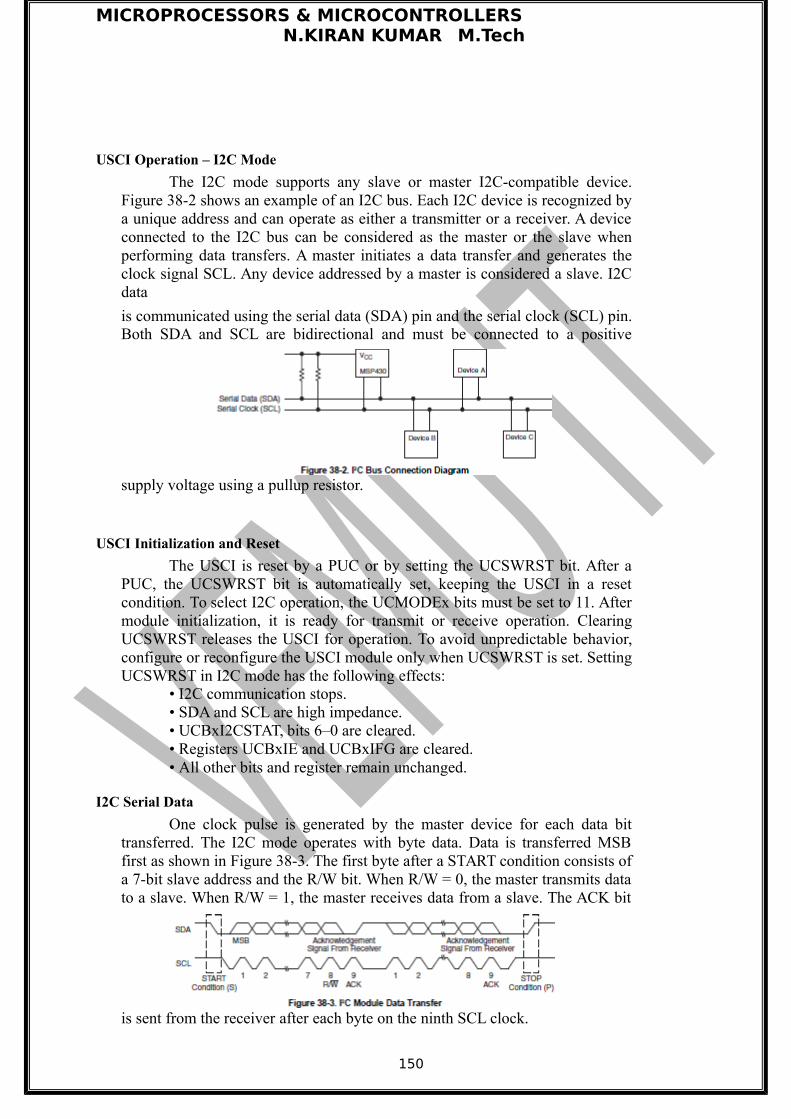
MICROPROCESSORS & MICROCONTROLLERSN.KIRAN KUMAR M.Tech
USCI Operation – I2C Mode
The I2C mode supports any slave or master I2C-compatible device.Figure 38-2 shows an example of an I2C bus. Each I2C device is recognized bya unique address and can operate as either a transmitter or a receiver. A deviceconnected to the I2C bus can be considered as the master or the slave whenperforming data transfers. A master initiates a data transfer and generates theclock signal SCL. Any device addressed by a master is considered a slave. I2Cdata
is communicated using the serial data (SDA) pin and the serial clock (SCL) pin.Both SDA and SCL are bidirectional and must be connected to a positive
supply voltage using a pullup resistor.
USCI Initialization and Reset
The USCI is reset by a PUC or by setting the UCSWRST bit. After aPUC, the UCSWRST bit is automatically set, keeping the USCI in a resetcondition. To select I2C operation, the UCMODEx bits must be set to 11. Aftermodule initialization, it is ready for transmit or receive operation. ClearingUCSWRST releases the USCI for operation. To avoid unpredictable behavior,configure or reconfigure the USCI module only when UCSWRST is set. SettingUCSWRST in I2C mode has the following effects:
• I2C communication stops.• SDA and SCL are high impedance.• UCBxI2CSTAT, bits 6–0 are cleared.• Registers UCBxIE and UCBxIFG are cleared.• All other bits and register remain unchanged.
I2C Serial Data
One clock pulse is generated by the master device for each data bittransferred. The I2C mode operates with byte data. Data is transferred MSBfirst as shown in Figure 38-3. The first byte after a START condition consists ofa 7-bit slave address and the R/W bit. When R/W = 0, the master transmits datato a slave. When R/W = 1, the master receives data from a slave. The ACK bit
is sent from the receiver after each byte on the ninth SCL clock.
150
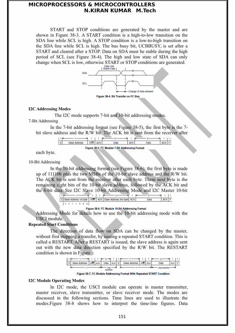
MICROPROCESSORS & MICROCONTROLLERSN.KIRAN KUMAR M.Tech
START and STOP conditions are generated by the master and areshown in Figure 38-3. A START condition is a high-to-low transition on theSDA line while SCL is high. A STOP condition is a low-to-high transition onthe SDA line while SCL is high. The bus busy bit, UCBBUSY, is set after aSTART and cleared after a STOP. Data on SDA must be stable during the highperiod of SCL (see Figure 38-4). The high and low state of SDA can onlychange when SCL is low, otherwise START or STOP conditions are generated.
I2C Addressing Modes
The I2C mode supports 7-bit and 10-bit addressing modes.7-Bit Addressing
In the 7-bit addressing format (see Figure 38-5), the first byte is the 7-bit slave address and the R/W bit. The ACK bit is sent from the receiver after
each byte.
10-Bit Addressing
In the 10-bit addressing format (see Figure 38-6), the first byte is madeup of 11110b plus the two MSBs of the 10-bit slave address and the R/W bit.The ACK bit is sent from the receiver after each byte. Them next byte is theremaining eight bits of the 10-bit slave address, followed by the ACK bit andthe 8-bit data. See I2C Slave 10-bit Addressing Mode and I2C Master 10-bit
Addressing Mode for details how to use the 10-bit addressing mode with theUSCI module.
Repeated Start Conditions
The direction of data flow on SDA can be changed by the master,without first stopping a transfer, by issuing a repeated START condition. This iscalled a RESTART. After a RESTART is issued, the slave address is again sentout with the new data direction specified by the R/W bit. The RESTARTcondition is shown in Figure
I2C Module Operating Modes
In I2C mode, the USCI module can operate in master transmitter,master receiver, slave transmitter, or slave receiver mode. The modes arediscussed in the following sections. Time lines are used to illustrate themodes.Figure 38-8 shows how to interpret the time-line figures. Data
151

MICROPROCESSORS & MICROCONTROLLERSN.KIRAN KUMAR M.Tech
transmitted by the master is represented by grey rectangles; data transmitted bythe slave is represented by white rectangles. Data transmitted by the USCImodule, either as master or slave, is shown by rectangles that are taller than theothers. Actions taken by the USCI module are shown in grey rectangles with anarrow indicating where in the data stream the action occurs. Actions that mustbe handled with software are indicated with white rectangles with an arrowpointing to where in the data stream the action must take place.
Slave Mode
The USCI module is configured as an I2C slave by selecting the I2Cmode with UCMODEx = 11 and UCSYNC = 1 and clearing the UCMST bit.Initially, the USCI module must to be configured in receiver mode by clearingthe UCTR bit to receive thenI2C address. Afterwards, transmit and receiveoperations are controlled automatically, depending on the R/W bit receivedtogether with the slave address.
The USCI slave address is programmed with the UCBxI2COA register.When UCA10 = 0, 7-bit addressing is selected. When UCA10 = 1, 10-bitaddressing is selected. The UCGCEN bit selects if the slave responds to ageneral call. When a START condition is detected on the
bus, the USCI module receives the transmitted address and compare it againstits own address stored in UCBxI2COA. The UCSTTIFG flag is set whenaddress received matches the USCI slave address.
I2C Slave Transmitter Mode
Slave transmitter mode is entered when the slave address transmitted bythe master is identical to its own address with a set R/W bit. The slavetransmitter shifts the serial data out on SDA with the clock pulses that aregenerated by the master device. The slave device does not generate the clock,but it does hold SCL low while intervention of the CPU is required after a bytehas been transmitted.If the master requests data from the slave, the USCI module is automaticallyconfigured as a transmitter and UCTR and UCTXIFG become set. The SCL
152
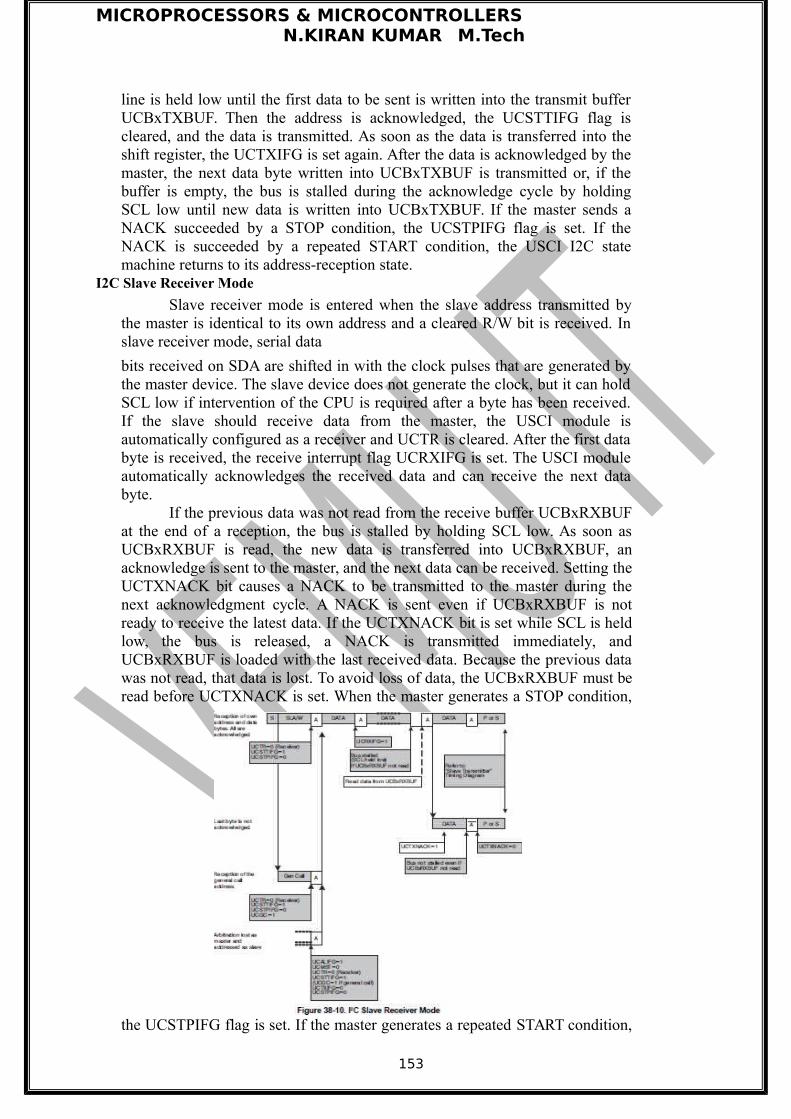
MICROPROCESSORS & MICROCONTROLLERSN.KIRAN KUMAR M.Tech
line is held low until the first data to be sent is written into the transmit bufferUCBxTXBUF. Then the address is acknowledged, the UCSTTIFG flag iscleared, and the data is transmitted. As soon as the data is transferred into theshift register, the UCTXIFG is set again. After the data is acknowledged by themaster, the next data byte written into UCBxTXBUF is transmitted or, if thebuffer is empty, the bus is stalled during the acknowledge cycle by holdingSCL low until new data is written into UCBxTXBUF. If the master sends aNACK succeeded by a STOP condition, the UCSTPIFG flag is set. If theNACK is succeeded by a repeated START condition, the USCI I2C statemachine returns to its address-reception state.
I2C Slave Receiver Mode
Slave receiver mode is entered when the slave address transmitted bythe master is identical to its own address and a cleared R/W bit is received. Inslave receiver mode, serial data
bits received on SDA are shifted in with the clock pulses that are generated bythe master device. The slave device does not generate the clock, but it can holdSCL low if intervention of the CPU is required after a byte has been received.If the slave should receive data from the master, the USCI module isautomatically configured as a receiver and UCTR is cleared. After the first databyte is received, the receive interrupt flag UCRXIFG is set. The USCI moduleautomatically acknowledges the received data and can receive the next databyte.
If the previous data was not read from the receive buffer UCBxRXBUFat the end of a reception, the bus is stalled by holding SCL low. As soon asUCBxRXBUF is read, the new data is transferred into UCBxRXBUF, anacknowledge is sent to the master, and the next data can be received. Setting theUCTXNACK bit causes a NACK to be transmitted to the master during thenext acknowledgment cycle. A NACK is sent even if UCBxRXBUF is notready to receive the latest data. If the UCTXNACK bit is set while SCL is heldlow, the bus is released, a NACK is transmitted immediately, andUCBxRXBUF is loaded with the last received data. Because the previous datawas not read, that data is lost. To avoid loss of data, the UCBxRXBUF must beread before UCTXNACK is set. When the master generates a STOP condition,
the UCSTPIFG flag is set. If the master generates a repeated START condition,
153
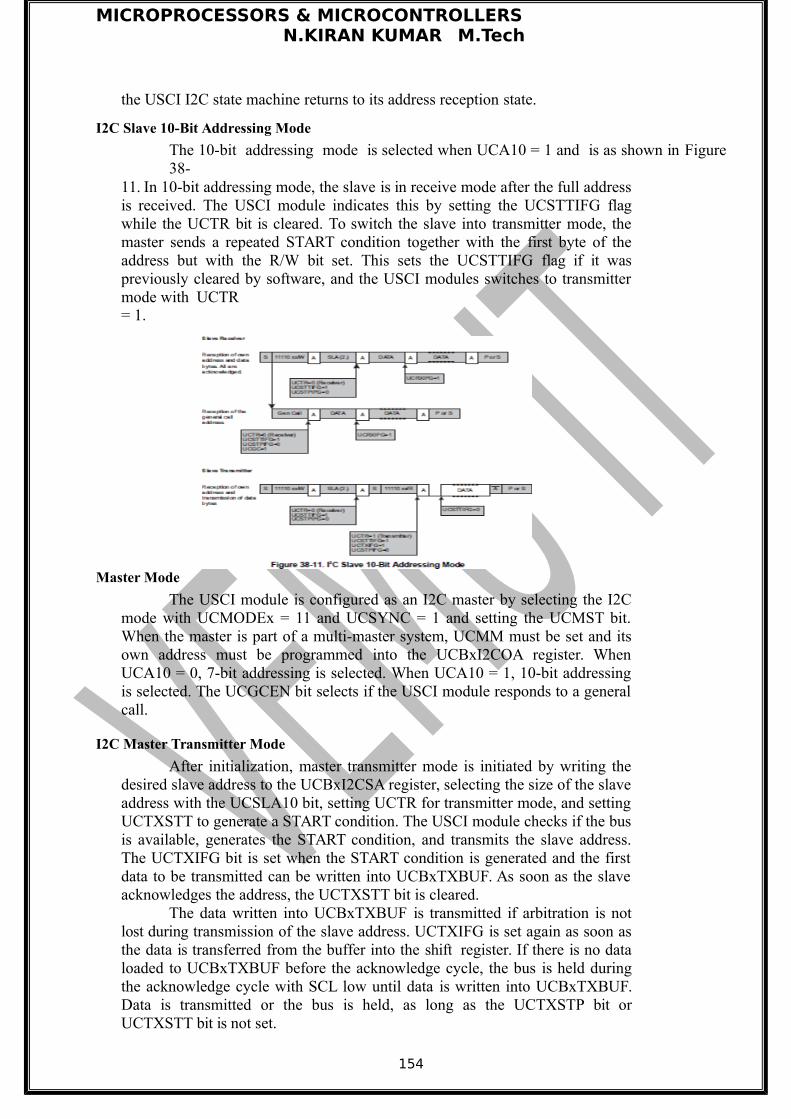
MICROPROCESSORS & MICROCONTROLLERSN.KIRAN KUMAR M.Tech
the USCI I2C state machine returns to its address reception state.
I2C Slave 10-Bit Addressing Mode
The 10-bit addressing mode is selected when UCA10 = 1 and is as shown in Figure38-
11. In 10-bit addressing mode, the slave is in receive mode after the full addressis received. The USCI module indicates this by setting the UCSTTIFG flagwhile the UCTR bit is cleared. To switch the slave into transmitter mode, themaster sends a repeated START condition together with the first byte of theaddress but with the R/W bit set. This sets the UCSTTIFG flag if it waspreviously cleared by software, and the USCI modules switches to transmittermode with UCTR= 1.
Master Mode
The USCI module is configured as an I2C master by selecting the I2Cmode with UCMODEx = 11 and UCSYNC = 1 and setting the UCMST bit.When the master is part of a multi-master system, UCMM must be set and itsown address must be programmed into the UCBxI2COA register. WhenUCA10 = 0, 7-bit addressing is selected. When UCA10 = 1, 10-bit addressingis selected. The UCGCEN bit selects if the USCI module responds to a generalcall.
I2C Master Transmitter Mode
After initialization, master transmitter mode is initiated by writing thedesired slave address to the UCBxI2CSA register, selecting the size of the slaveaddress with the UCSLA10 bit, setting UCTR for transmitter mode, and settingUCTXSTT to generate a START condition. The USCI module checks if the busis available, generates the START condition, and transmits the slave address.The UCTXIFG bit is set when the START condition is generated and the firstdata to be transmitted can be written into UCBxTXBUF. As soon as the slaveacknowledges the address, the UCTXSTT bit is cleared.
The data written into UCBxTXBUF is transmitted if arbitration is notlost during transmission of the slave address. UCTXIFG is set again as soon asthe data is transferred from the buffer into the shift register. If there is no dataloaded to UCBxTXBUF before the acknowledge cycle, the bus is held duringthe acknowledge cycle with SCL low until data is written into UCBxTXBUF.Data is transmitted or the bus is held, as long as the UCTXSTP bit orUCTXSTT bit is not set.
154
MICROPROCESSORS & MICROCONTROLLERSN.KIRAN KUMAR M.Tech
Setting UCTXSTP generates a STOP condition after the nextacknowledge from the slave. If UCTXSTP is set during the transmission of theslave's address or while the USCI module waits for data to be written intoUCBxTXBUF, a STOP condition is generated, even if no data was transmittedto the slave. When transmitting a single byte of data, the UCTXSTP bit must beset while the byte is being transmitted or anytime after transmission begins,without writing new data into UCBxTXBUF. Otherwise, only the address istransmitted. When the data is transferred from the buffer to the shift register,UCTXIFG is set, indicating data transmission has begun, and the UCTXSTP bitmay be set.
Setting UCTXSTT generates a repeated START condition. In this case,UCTR may be set or cleared to configure transmitter or receiver, and adifferent slave address may be written into UCBxI2CSA if desired. If the slavedoes not acknowledge the transmitted data, the not- acknowledge interrupt flagUCNACKIFG is set. The master must react with either a STOP condition or arepeated START condition. If data was already written into UCBxTXBUF, it is
discarded. If this data should be transmitted after a repeated START, it must bewritten into UCBxTXBUF again. Any set UCTXSTT is also discarded. Totrigger a repeated START, UCTXSTT must be set again.
I2C Master Receiver Mode
After initialization, master receiver mode is initiated by writing thedesired slave address to the UCBxI2CSA register, selecting the size of the slaveaddress with the UCSLA10 bit, clearing UCTR for receiver mode, and settingUCTXSTT to generate a START condition.
The USCI module checks if the bus is available, generates the STARTcondition, and transmits the slave address. As soon as the slave acknowledgesthe address, the UCTXSTT bit is cleared. After the acknowledge of the addressfrom the slave, the first data byte from the slave is received and acknowledgedand the UCRXIFG flag is set. Data is received from the slave, as long asUCTXSTP orUCTXSTT is not set. If UCBxRXBUF is not read, the master holds the busduring reception of the last data bit and until the UCBxRXBUF is read. If theslave does not acknowledge the transmitted address, the not-acknowledgeinterrupt flag
UCNACKIFG is set. The master must react with either a STOPcondition or a repeated START condition. Setting the UCTXSTP bit generatesa STOP condition. After setting UCTXSTP, a NACK followed by a STOPcondition is generated after reception of the data from the slave, or immediatelyif the USCI module is currently waiting for UCBxRXBUF to be read. If amaster wants to receive a single byte only, the UCTXSTP bit must be set whilethe byte is being received. For this case, the UCTXSTT may be polled todetermine when it is cleared:
BIS.B #UCTXSTT, &UCB0CTL1 ;Transmit STARTcond. POLL_STT BIT.B #UCTXSTT,&UCB0CTL1 ;Poll UCTXSTT bitJC POLL_STT ;When cleared,BIS.B #UCTXSTP, &UCB0CTL1 ;transmit STOP cond.
Setting UCTXSTT generates a repeated START condition. In this case, UCTRmay be set or cleared to configure transmitter or receiver, and a different slaveaddress may be written into UCBxI2CSA if desired.
155
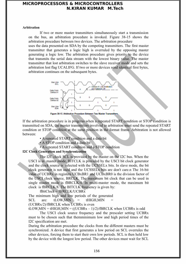
MICROPROCESSORS & MICROCONTROLLERSN.KIRAN KUMAR M.Tech
Arbitration
If two or more master transmitters simultaneously start a transmissionon the bus, an arbitration procedure is invoked. Figure 38-15 shows thearbitration procedure between two devices. The arbitration procedureuses the data presented on SDA by the competing transmitters. The first mastertransmitter that generates a logic high is overruled by the opposing mastergenerating a logic low. The arbitration procedure gives priority to the devicethat transmits the serial data stream with the lowest binary value. The mastertransmitter that lost arbitration switches to the slave receiver mode and sets thearbitration lost flag UCALIFG. If two or more devices send identical first bytes,arbitration continues on the subsequent bytes.
If the arbitration procedure is in progress when a repeated START condition or STOP condition istransmitted on SDA, the master transmitters involved in arbitration must send the repeated STARTcondition or STOP condition at the same position in the format frame. Arbitration is not allowedbetween:
• A repeated START condition and a data bit• A STOP condition and a data bit• A repeated START condition and a STOP condition
I2C Clock Generation and Synchronization
The I2C clock SCL is provided by the master on the I2C bus. When theUSCI is in master mode, BITCLK is provided by the USCI bit clock generatorand the clock source is selected with the UCSSELx bits. In slave mode, the bitclock generator is not used and the UCSSELx bits are don't care.n The 16-bitvalue of UCBRx in registers UCBxBR1 and UCBxBR0 is the division factor ofthe USCI clock source, BRCLK. The maximum bit clock that can be used insingle master mode is fBRCLK/4. In multi-master mode, the maximum bitclock is fBRCLK/8. The BITCLK frequency is given by:
fBitClock = fBRCLK/UCBRxThe minimum high and low periods of the generatedSCL are: tLOW,MIN = tHIGH,MIN =(UCBRx/2)/fBRCLK when UCBRx is eventLOW,MIN = tHIGH,MIN = ((UCBRx – 1)/2)/fBRCLK when UCBRx is odd
The USCI clock source frequency and the prescaler setting UCBRxmust to be chosen such that themminimum low and high period times of theI2C specification are met.During the arbitration procedure the clocks from the different masters must besynchronized. A device that first generates a low period on SCL overrules theother devices, forcing them to start their own low periods. SCL is then held lowby the device with the longest low period. The other devices must wait for SCL
156
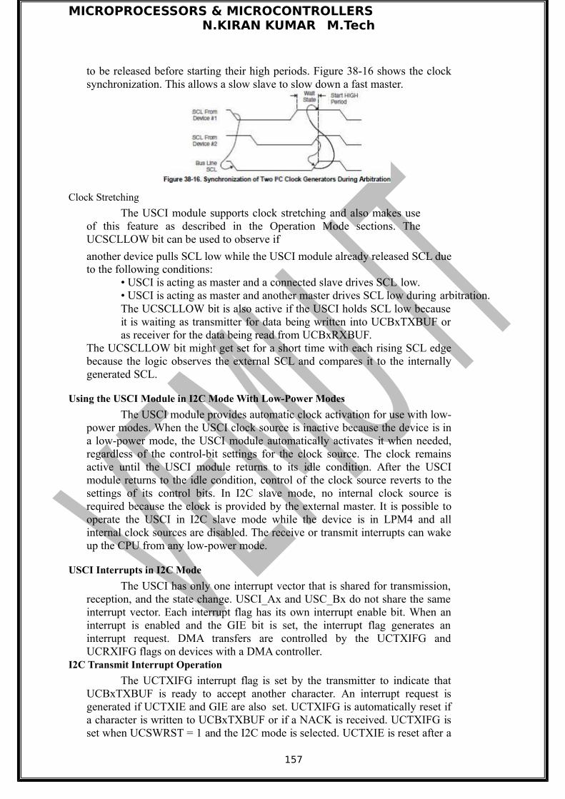
MICROPROCESSORS & MICROCONTROLLERSN.KIRAN KUMAR M.Tech
to be released before starting their high periods. Figure 38-16 shows the clocksynchronization. This allows a slow slave to slow down a fast master.
Clock Stretching
The USCI module supports clock stretching and also makes useof this feature as described in the Operation Mode sections. TheUCSCLLOW bit can be used to observe if
another device pulls SCL low while the USCI module already released SCL dueto the following conditions:
• USCI is acting as master and a connected slave drives SCL low.• USCI is acting as master and another master drives SCL low during arbitration.The UCSCLLOW bit is also active if the USCI holds SCL low becauseit is waiting as transmitter for data being written into UCBxTXBUF oras receiver for the data being read from UCBxRXBUF.
The UCSCLLOW bit might get set for a short time with each rising SCL edgebecause the logic observes the external SCL and compares it to the internallygenerated SCL.
Using the USCI Module in I2C Mode With Low-Power Modes
The USCI module provides automatic clock activation for use with low-power modes. When the USCI clock source is inactive because the device is ina low-power mode, the USCI module automatically activates it when needed,regardless of the control-bit settings for the clock source. The clock remainsactive until the USCI module returns to its idle condition. After the USCImodule returns to the idle condition, control of the clock source reverts to thesettings of its control bits. In I2C slave mode, no internal clock source isrequired because the clock is provided by the external master. It is possible tooperate the USCI in I2C slave mode while the device is in LPM4 and allinternal clock sources are disabled. The receive or transmit interrupts can wakeup the CPU from any low-power mode.
USCI Interrupts in I2C Mode
The USCI has only one interrupt vector that is shared for transmission,reception, and the state change. USCI_Ax and USC_Bx do not share the sameinterrupt vector. Each interrupt flag has its own interrupt enable bit. When aninterrupt is enabled and the GIE bit is set, the interrupt flag generates aninterrupt request. DMA transfers are controlled by the UCTXIFG andUCRXIFG flags on devices with a DMA controller.
I2C Transmit Interrupt Operation
The UCTXIFG interrupt flag is set by the transmitter to indicate thatUCBxTXBUF is ready to accept another character. An interrupt request isgenerated if UCTXIE and GIE are also set. UCTXIFG is automatically reset ifa character is written to UCBxTXBUF or if a NACK is received. UCTXIFG isset when UCSWRST = 1 and the I2C mode is selected. UCTXIE is reset after a
157
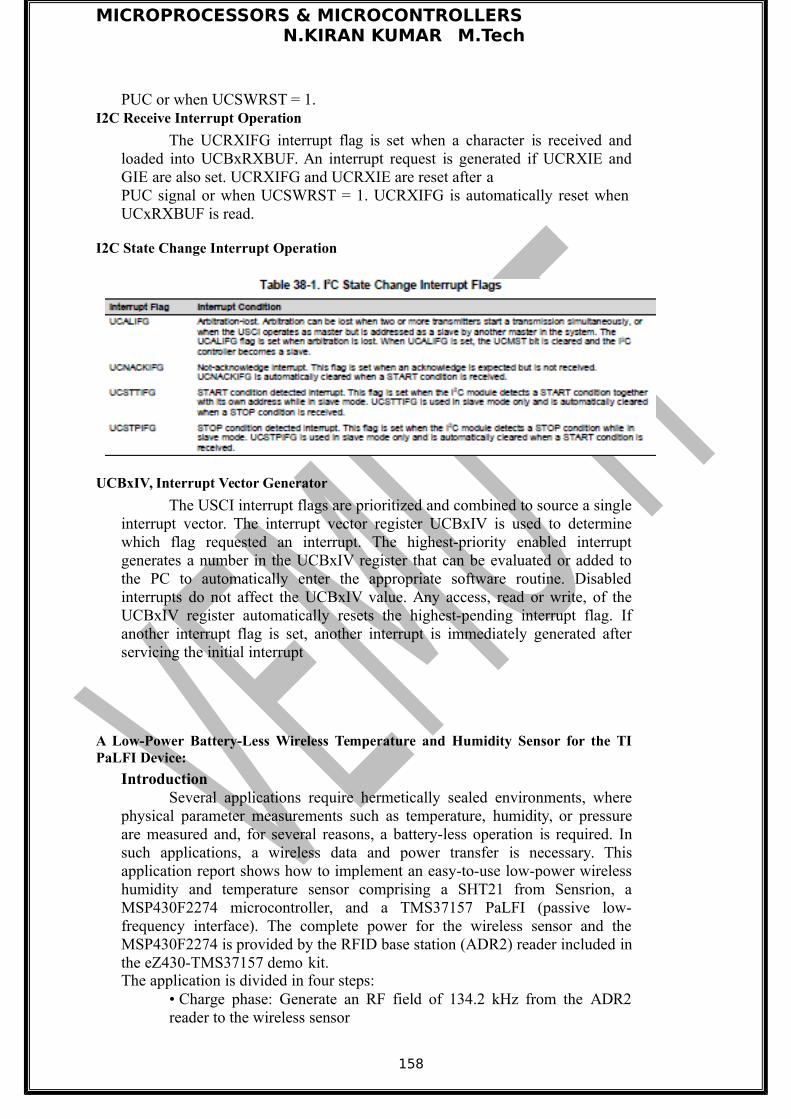
MICROPROCESSORS & MICROCONTROLLERSN.KIRAN KUMAR M.Tech
PUC or when UCSWRST = 1.I2C Receive Interrupt Operation
The UCRXIFG interrupt flag is set when a character is received andloaded into UCBxRXBUF. An interrupt request is generated if UCRXIE andGIE are also set. UCRXIFG and UCRXIE are reset after aPUC signal or when UCSWRST = 1. UCRXIFG is automatically reset whenUCxRXBUF is read.
I2C State Change Interrupt Operation
UCBxIV, Interrupt Vector Generator
The USCI interrupt flags are prioritized and combined to source a singleinterrupt vector. The interrupt vector register UCBxIV is used to determinewhich flag requested an interrupt. The highest-priority enabled interruptgenerates a number in the UCBxIV register that can be evaluated or added tothe PC to automatically enter the appropriate software routine. Disabledinterrupts do not affect the UCBxIV value. Any access, read or write, of theUCBxIV register automatically resets the highest-pending interrupt flag. Ifanother interrupt flag is set, another interrupt is immediately generated afterservicing the initial interrupt
A Low-Power Battery-Less Wireless Temperature and Humidity Sensor for the TIPaLFI Device:
IntroductionSeveral applications require hermetically sealed environments, where
physical parameter measurements such as temperature, humidity, or pressureare measured and, for several reasons, a battery-less operation is required. Insuch applications, a wireless data and power transfer is necessary. Thisapplication report shows how to implement an easy-to-use low-power wirelesshumidity and temperature sensor comprising a SHT21 from Sensrion, aMSP430F2274 microcontroller, and a TMS37157 PaLFI (passive low-frequency interface). The complete power for the wireless sensor and theMSP430F2274 is provided by the RFID base station (ADR2) reader included inthe eZ430-TMS37157 demo kit.The application is divided in four steps:
• Charge phase: Generate an RF field of 134.2 kHz from the ADR2reader to the wireless sensor
158
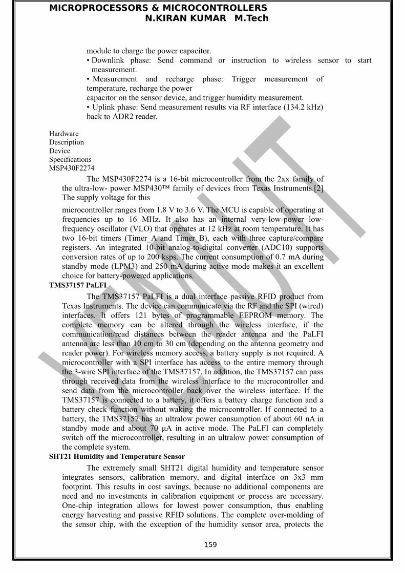
MICROPROCESSORS & MICROCONTROLLERSN.KIRAN KUMAR M.Tech
module to charge the power capacitor.• Downlink phase: Send command or instruction to wireless sensor to start
measurement.• Measurement and recharge phase: Trigger measurement oftemperature, recharge the powercapacitor on the sensor device, and trigger humidity measurement.• Uplink phase: Send measurement results via RF interface (134.2 kHz)back to ADR2 reader.
HardwareDescriptionDeviceSpecificationsMSP430F2274
The MSP430F2274 is a 16-bit microcontroller from the 2xx family ofthe ultra-low- power MSP430™ family of devices from Texas Instruments.[2]The supply voltage for this
microcontroller ranges from 1.8 V to 3.6 V. The MCU is capable of operating atfrequencies up to 16 MHz. It also has an internal very-low-power low-frequency oscillator (VLO) that operates at 12 kHz at room temperature. It hastwo 16-bit timers (Timer_A and Timer_B), each with three capture/compareregisters. An integrated 10-bit analog-to-digital converter (ADC10) supportsconversion rates of up to 200 ksps. The current consumption of 0.7 mA duringstandby mode (LPM3) and 250 mA during active mode makes it an excellentchoice for battery-powered applications.
TMS37157 PaLFI
The TMS37157 PaLFI is a dual interface passive RFID product fromTexas Instruments. The device can communicate via the RF and the SPI (wired)interfaces. It offers 121 bytes of programmable EEPROM memory. Thecomplete memory can be altered through the wireless interface, if thecommunication/read distances between the reader antenna and the PaLFIantenna are less than 10 cm to 30 cm (depending on the antenna geometry andreader power). For wireless memory access, a battery supply is not required. Amicrocontroller with a SPI interface has access to the entire memory throughthe 3-wire SPI interface of the TMS37157. In addition, the TMS37157 can passthrough received data from the wireless interface to the microcontroller andsend data from the microcontroller back over the wireless interface. If theTMS37157 is connected to a battery, it offers a battery charge function and abattery check function without waking the microcontroller. If connected to abattery, the TMS37157 has an ultralow power consumption of about 60 nA instandby mode and about 70 μA in active mode. The PaLFI can completelyswitch off the microcontroller, resulting in an ultralow power consumption ofthe complete system.
SHT21 Humidity and Temperature Sensor
The extremely small SHT21 digital humidity and temperature sensorintegrates sensors, calibration memory, and digital interface on 3x3 mmfootprint. This results in cost savings, because no additional components areneed and no investments in calibration equipment or process are necessary.One-chip integration allows for lowest power consumption, thus enablingenergy harvesting and passive RFID solutions. The complete over-molding ofthe sensor chip, with the exception of the humidity sensor area, protects the
159
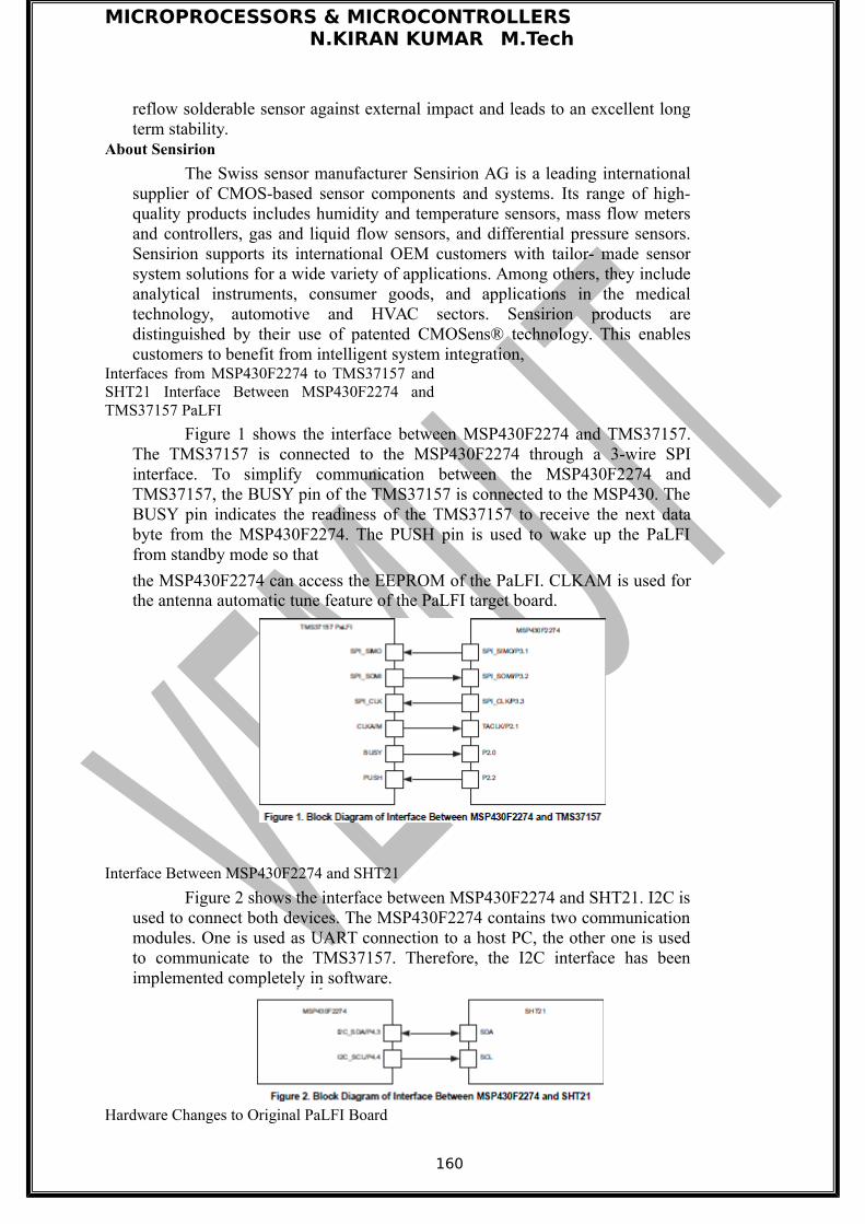
MICROPROCESSORS & MICROCONTROLLERSN.KIRAN KUMAR M.Tech
reflow solderable sensor against external impact and leads to an excellent longterm stability.
About Sensirion
The Swiss sensor manufacturer Sensirion AG is a leading internationalsupplier of CMOS-based sensor components and systems. Its range of high-quality products includes humidity and temperature sensors, mass flow metersand controllers, gas and liquid flow sensors, and differential pressure sensors.Sensirion supports its international OEM customers with tailor- made sensorsystem solutions for a wide variety of applications. Among others, they includeanalytical instruments, consumer goods, and applications in the medicaltechnology, automotive and HVAC sectors. Sensirion products aredistinguished by their use of patented CMOSens® technology. This enablescustomers to benefit from intelligent system integration,
Interfaces from MSP430F2274 to TMS37157 andSHT21 Interface Between MSP430F2274 andTMS37157 PaLFI
Figure 1 shows the interface between MSP430F2274 and TMS37157.The TMS37157 is connected to the MSP430F2274 through a 3-wire SPIinterface. To simplify communication between the MSP430F2274 andTMS37157, the BUSY pin of the TMS37157 is connected to the MSP430. TheBUSY pin indicates the readiness of the TMS37157 to receive the next databyte from the MSP430F2274. The PUSH pin is used to wake up the PaLFIfrom standby mode so that
the MSP430F2274 can access the EEPROM of the PaLFI. CLKAM is used forthe antenna automatic tune feature of the PaLFI target board.
Interface Between MSP430F2274 and SHT21
Figure 2 shows the interface between MSP430F2274 and SHT21. I2C isused to connect both devices. The MSP430F2274 contains two communicationmodules. One is used as UART connection to a host PC, the other one is usedto communicate to the TMS37157. Therefore, the I2C interface has beenimplemented completely in software.
Hardware Changes to Original PaLFI Board
160
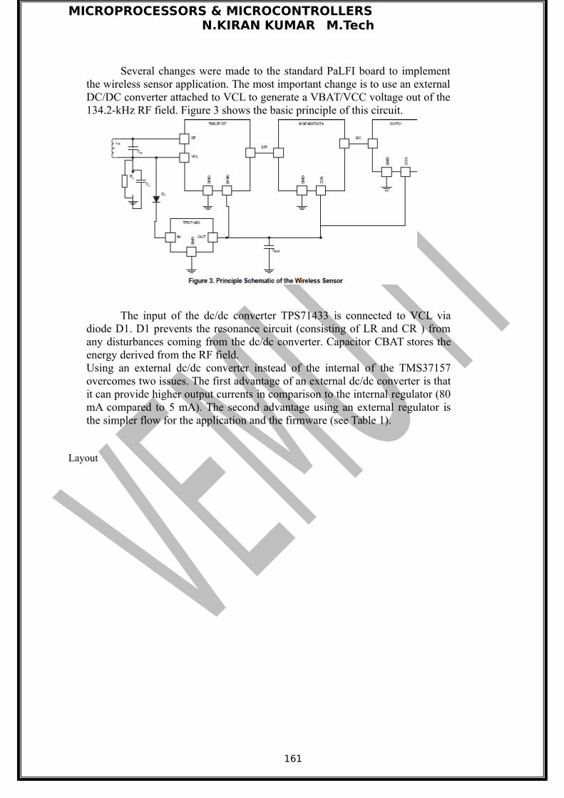
MICROPROCESSORS & MICROCONTROLLERSN.KIRAN KUMAR M.Tech
Several changes were made to the standard PaLFI board to implementthe wireless sensor application. The most important change is to use an externalDC/DC converter attached to VCL to generate a VBAT/VCC voltage out of the134.2-kHz RF field. Figure 3 shows the basic principle of this circuit.
The input of the dc/dc converter TPS71433 is connected to VCL viadiode D1. D1 prevents the resonance circuit (consisting of LR and CR ) fromany disturbances coming from the dc/dc converter. Capacitor CBAT stores theenergy derived from the RF field.Using an external dc/dc converter instead of the internal of the TMS37157overcomes two issues. The first advantage of an external dc/dc converter is thatit can provide higher output currents in comparison to the internal regulator (80mA compared to 5 mA). The second advantage using an external regulator isthe simpler flow for the application and the firmware (see Table 1).
Layout
161
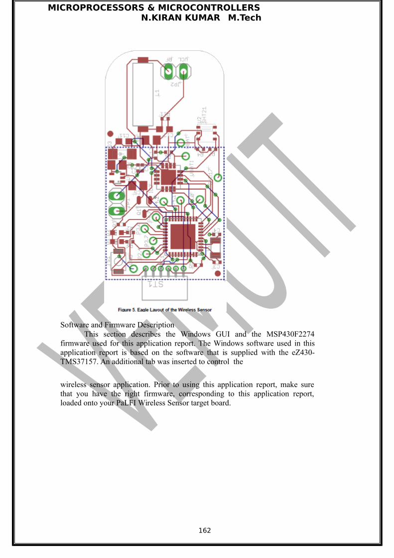
MICROPROCESSORS & MICROCONTROLLERSN.KIRAN KUMAR M.Tech
Software and Firmware DescriptionThis section describes the Windows GUI and the MSP430F2274
firmware used for this application report. The Windows software used in thisapplication report is based on the software that is supplied with the eZ430-TMS37157. An additional tab was inserted to control the
wireless sensor application. Prior to using this application report, make surethat you have the right firmware, corresponding to this application report,loaded onto your PaLFI Wireless Sensor target board.
162