lecture #5 (electronics)
DESCRIPTION
Electronics lectureTRANSCRIPT

2
Class C power amplifier design
• There are four important design parameters are of great importance for PA design in general
• These parameters are
– The output power
– Transistor power dissipation
– Maximum collector to emitter voltage VCEmax
– The maximum transistor output current Ip
3
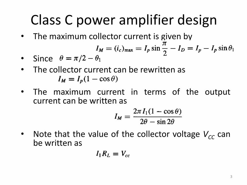
Class C power amplifier design • The maximum collector current is given by
• Since • The collector current can be rewritten as
• The maximum current in terms of the output
current can be written as
• Note that the value of the collector voltage VCC can be written as
4
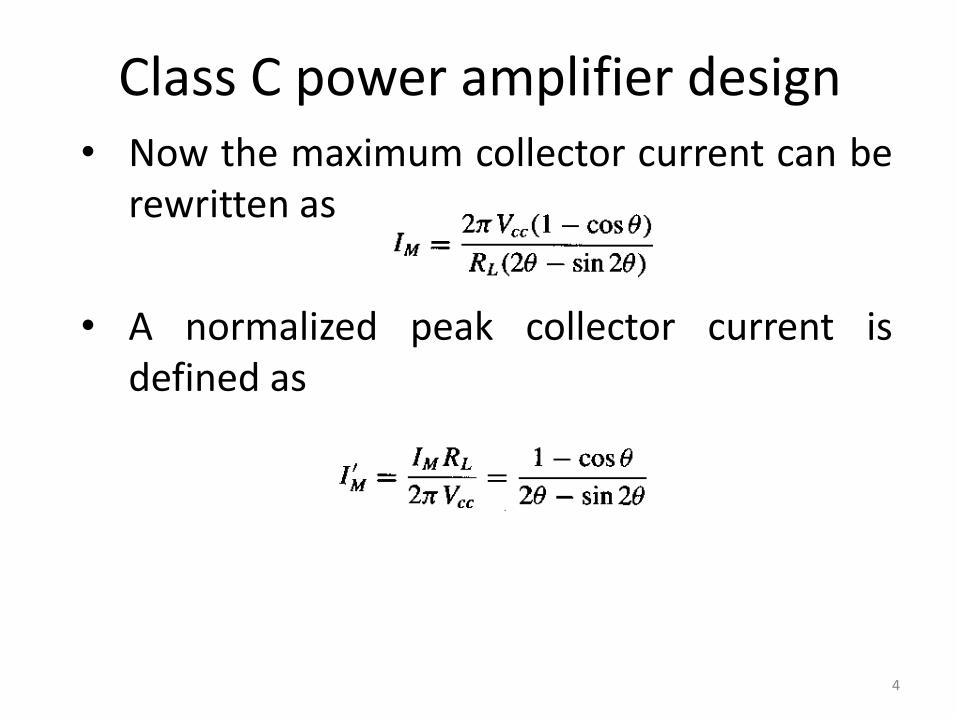
Class C power amplifier design • Now the maximum collector current can be
rewritten as
• A normalized peak collector current is defined as
5
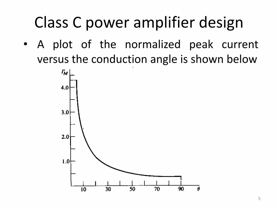
Class C power amplifier design • A plot of the normalized peak current
versus the conduction angle is shown below
6
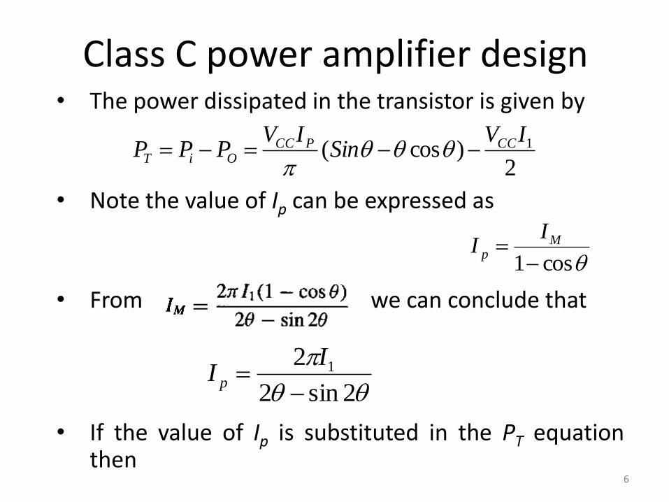
Class C power amplifier design • The power dissipated in the transistor is given by
• Note the value of Ip can be expressed as
• From we can conclude that
• If the value of Ip is substituted in the PT equation then
2)cos( 1IV
SinIV
PPP CCPCCOiT
cos1 M
p
II
2sin2
2 1
II p
7
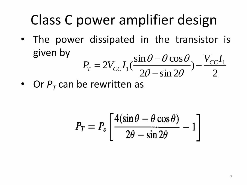
Class C power amplifier design • The power dissipated in the transistor is
given by
• Or PT can be rewritten as
2)
2sin2
cossin(2 1
1
IVIVP CC
CCT
8
Class C power amplifier design
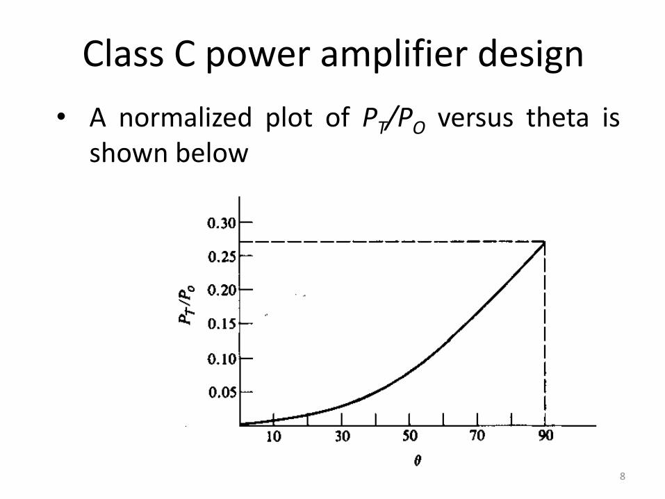
• A normalized plot of PT/PO versus theta is shown below
9
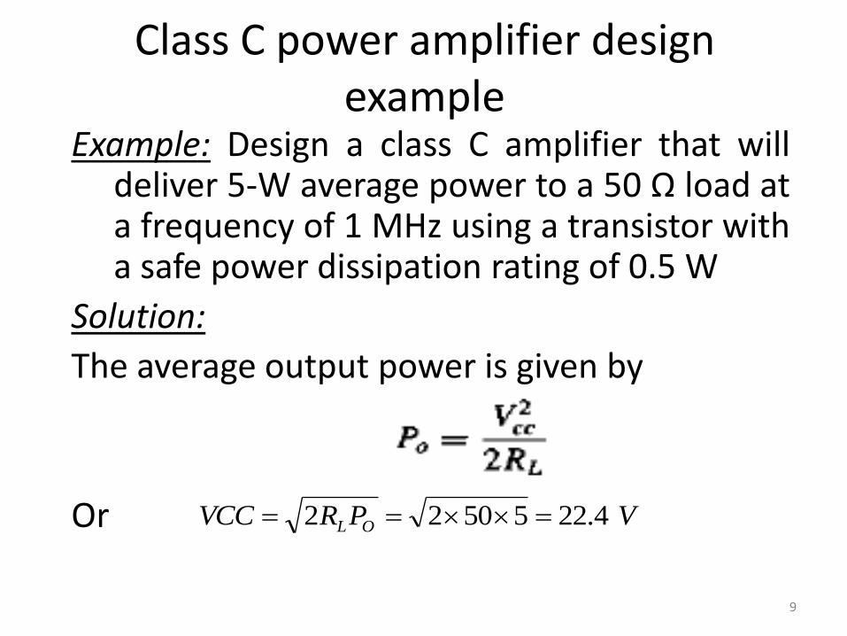
Class C power amplifier design example
Example: Design a class C amplifier that will deliver 5-W average power to a 50 Ω load at a frequency of 1 MHz using a transistor with a safe power dissipation rating of 0.5 W
Solution:
The average output power is given by
Or
VPRVCC OL 4.2255022
10
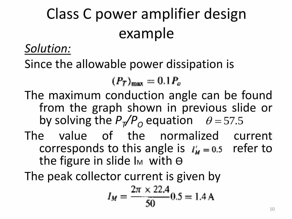
Class C power amplifier design example
Solution: Since the allowable power dissipation is The maximum conduction angle can be found
from the graph shown in previous slide or by solving the PT/PO equation
The value of the normalized current corresponds to this angle is refer to the figure in slide IM with ϴ
The peak collector current is given by
5.57
11
Class C power amplifier design
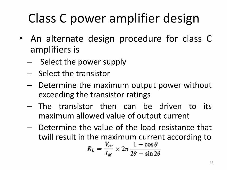
• An alternate design procedure for class C amplifiers is
– Select the power supply
– Select the transistor
– Determine the maximum output power without exceeding the transistor ratings
– The transistor then can be driven to its maximum allowed value of output current
– Determine the value of the load resistance that twill result in the maximum current according to
12
Class C power amplifier design
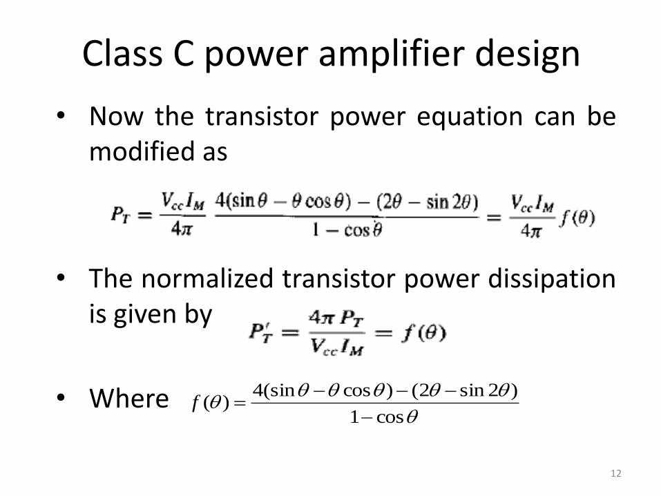
• Now the transistor power equation can be modified as
• The normalized transistor power dissipation is given by
• Where
cos1
)2sin2()cos(sin4)(
f
13
Class C power amplifier design
14
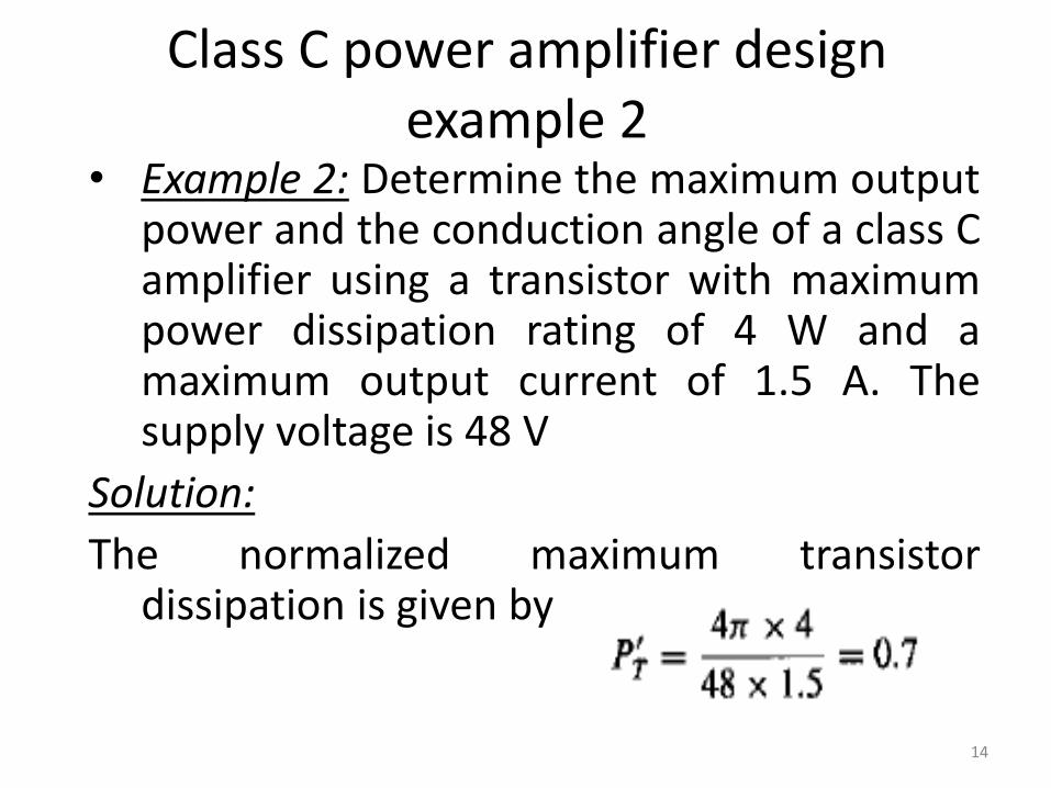
Class C power amplifier design example 2
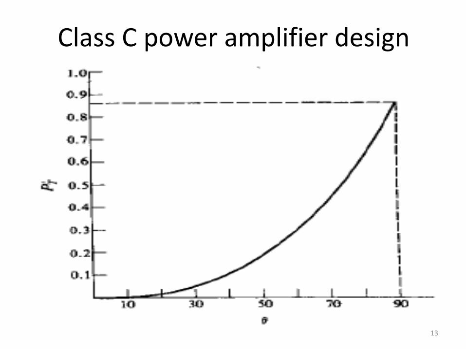
• Example 2: Determine the maximum output power and the conduction angle of a class C amplifier using a transistor with maximum power dissipation rating of 4 W and a maximum output current of 1.5 A. The supply voltage is 48 V
Solution:
The normalized maximum transistor dissipation is given by
15
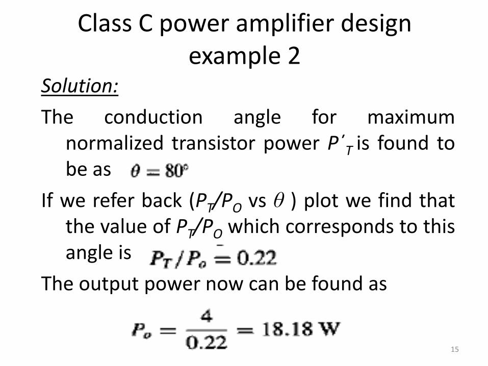
Class C power amplifier design example 2
Solution:
The conduction angle for maximum normalized transistor power P΄T is found to be as
If we refer back (PT/PO vs θ ) plot we find that the value of PT/PO which corresponds to this angle is
The output power now can be found as
16
Class C power amplifier design example 2
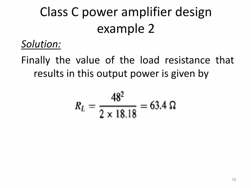
Solution:
Finally the value of the load resistance that results in this output power is given by

Summary
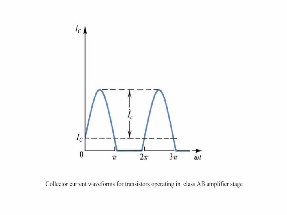
Class B
• A class B output stage can be far more efficient than a class A stage (78.5 % maximum efficiency compared with 25 %).
• It also requires twice as many output transistors…
• …and it isn’t very linear; cross-over distortion can be significant.
Class B • Class B amplifiers are used in low cost designs or
designs where sound quality is not that important.
• Class B amplifiers are significantly more efficient than class A amps.
• They suffer from bad distortion when the signal level is low (the distortion in this region of operation is called "crossover distortion").
Class B • Class B is used most often where economy of design
is needed.
• Before the advent of IC amplifiers, class B amplifiers were common in clock radio circuits, pocket transistor radios, or other applications where quality of sound is not that critical.
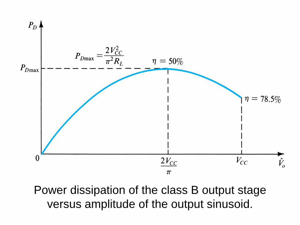
Power dissipation of the class B output stage
versus amplitude of the output sinusoid.
Class AB • Class AB is probably the most common amplifier
class currently used in home stereo and similar amplifiers.
• Class AB amps combine the good points of class A and B amps.
• They have the improved efficiency of class B amps and distortion performance that is a lot closer to that of a class A amp.

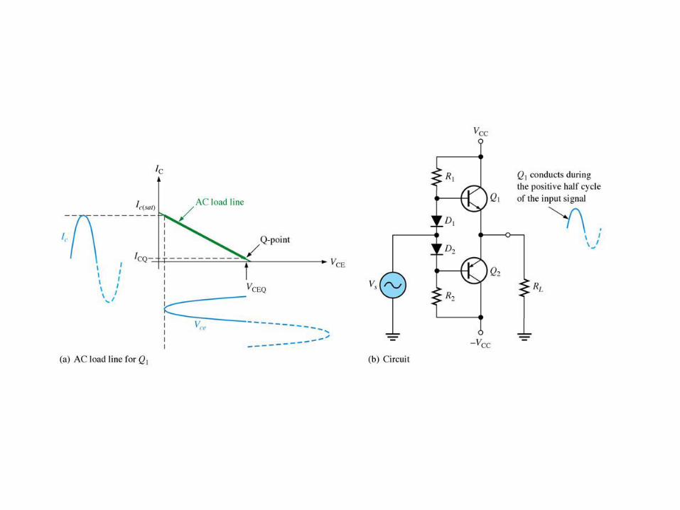
Eliminating crossover distortion in a transformer-coupled push-pull amplifier. The diode compensates for the base-emitter drop of the transistors and produces
class AB operation.
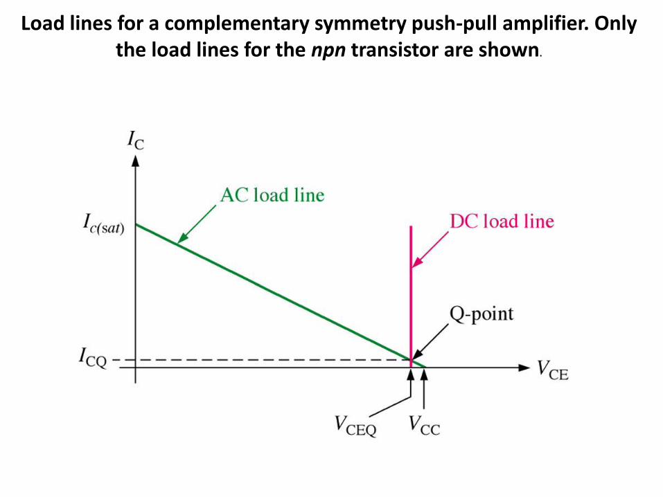
Load lines for a complementary symmetry push-pull amplifier. Only the load lines for the npn transistor are shown.

Single-ended push-pull amplifier.


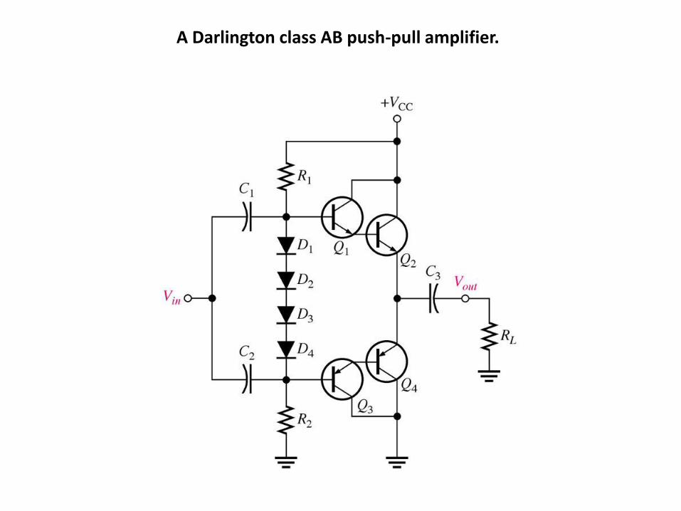
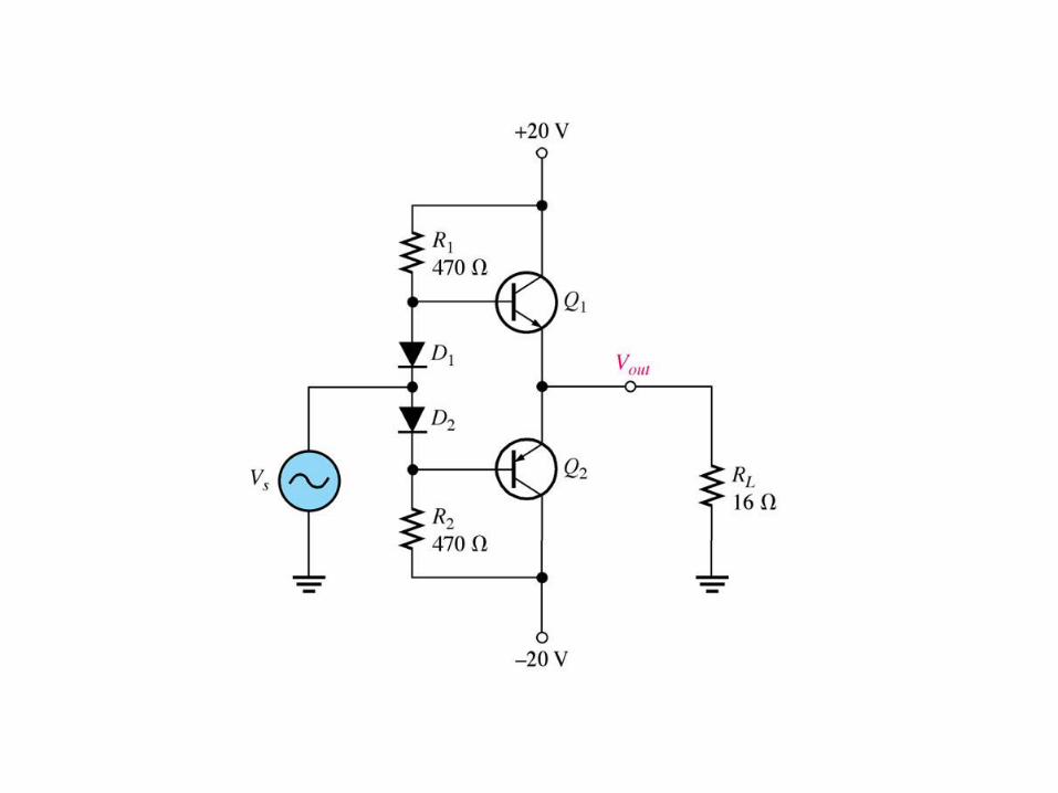
A Darlington class AB push-pull amplifier.
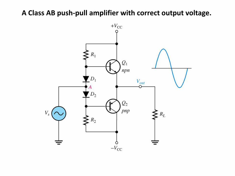
A Class AB push-pull amplifier with correct output voltage.
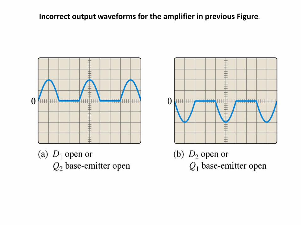
Incorrect output waveforms for the amplifier in previous Figure.
Class AB
• With such amplifiers, distortion is worst when the signal is low, and generally lowest when the signal is just reaching the point of clipping.
• Class AB amps use pairs of transistors, both of them being biased slightly ON so that the crossover distortion (associated with Class B amps) is largely eliminated.
Class C • Class C amps are never used for audio circuits.
• They are commonly used in RF circuits.
• Class C amplifiers operate the output transistor in a state that results in tremendous distortion (it would be totally unsuitable for audio reproduction).

Basic class C amplifier operation (non inverting).

Basic class C operation.
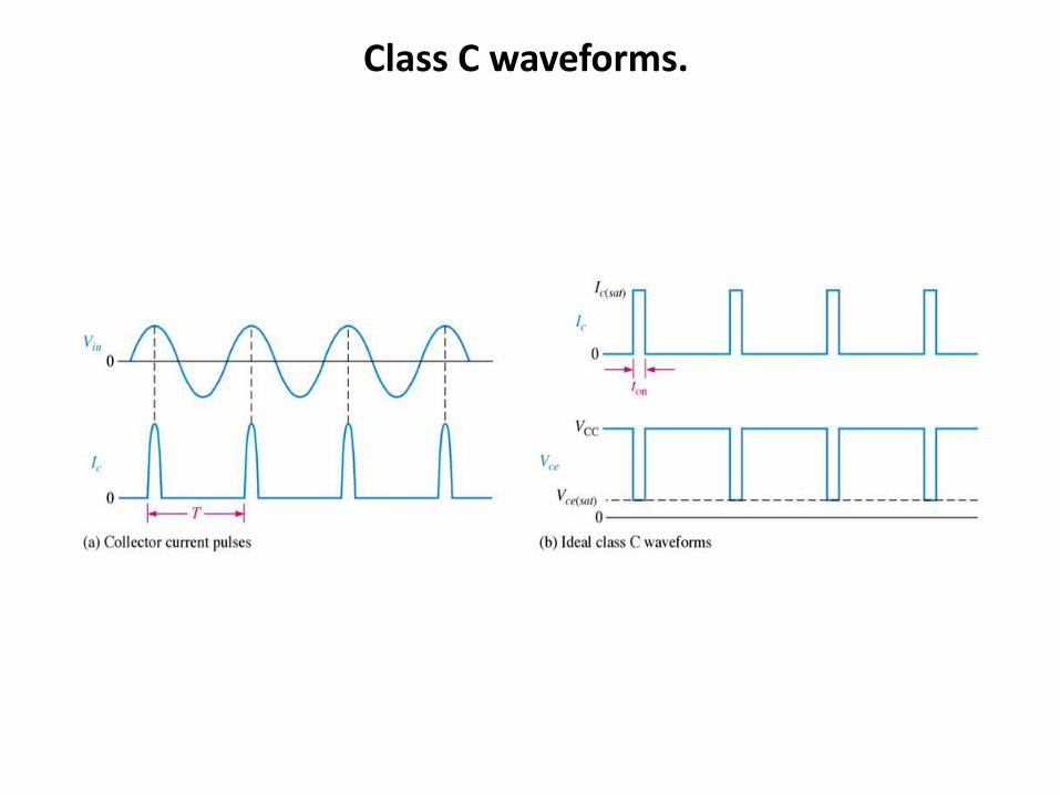
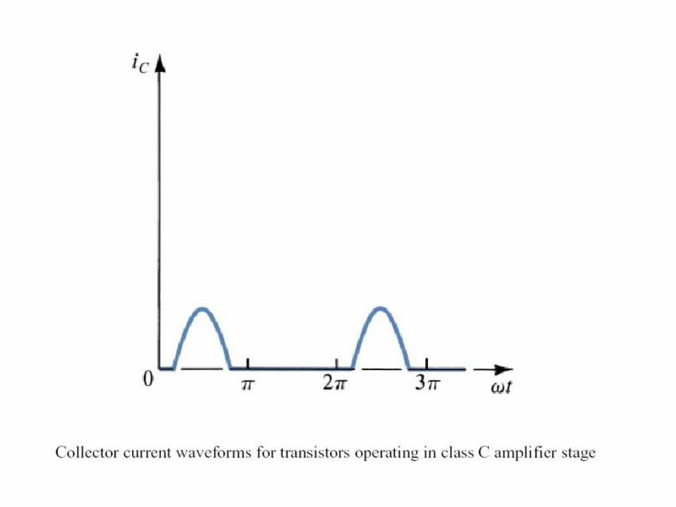
Class C waveforms.
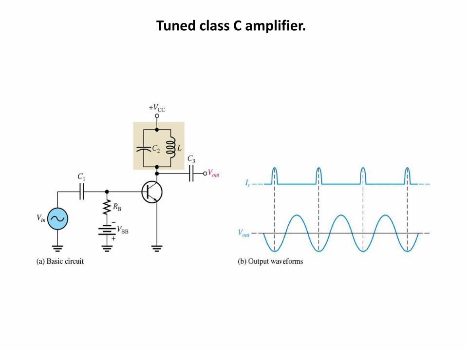
Tuned class C amplifier.
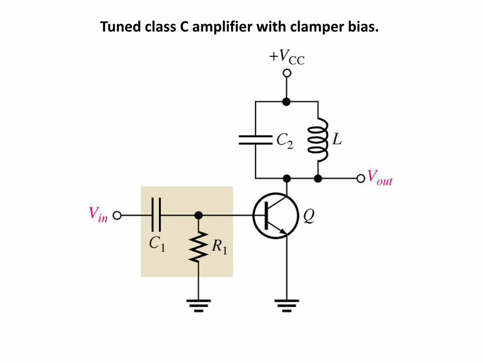
Tuned class C amplifier with clamper bias.
Class C
• However, the RF circuits where Class C amps are used, employ filtering so that the final signal is completely acceptable.
• Class C amps are quite efficient.
Power Transistor Limitations

POWER TRANSISTOR
Transistor limitations
• Maximum rated current,
• Maximum rated voltage,
• Maximum rated power.
The maximum rated power is related to the maximum
allowable temperature of the transistor.
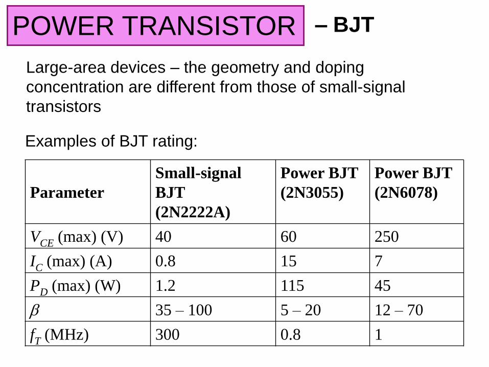
– BJT
Large-area devices – the geometry and doping
concentration are different from those of small-signal
transistors
Examples of BJT rating:
Parameter
Small-signal
BJT
(2N2222A)
Power BJT
(2N3055)
Power BJT
(2N6078)
VCE (max) (V) 40 60 250
IC (max) (A) 0.8 15 7
PD (max) (W) 1.2 115 45
35 – 100 5 – 20 12 – 70
fT (MHz) 300 0.8 1
POWER TRANSISTOR
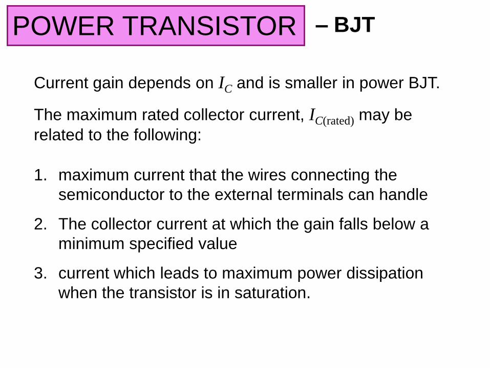
Current gain depends on IC and is smaller in power BJT.
The maximum rated collector current, IC(rated) may be
related to the following:
1. maximum current that the wires connecting the
semiconductor to the external terminals can handle
2. The collector current at which the gain falls below a
minimum specified value
3. current which leads to maximum power dissipation
when the transistor is in saturation.
– BJT POWER TRANSISTOR
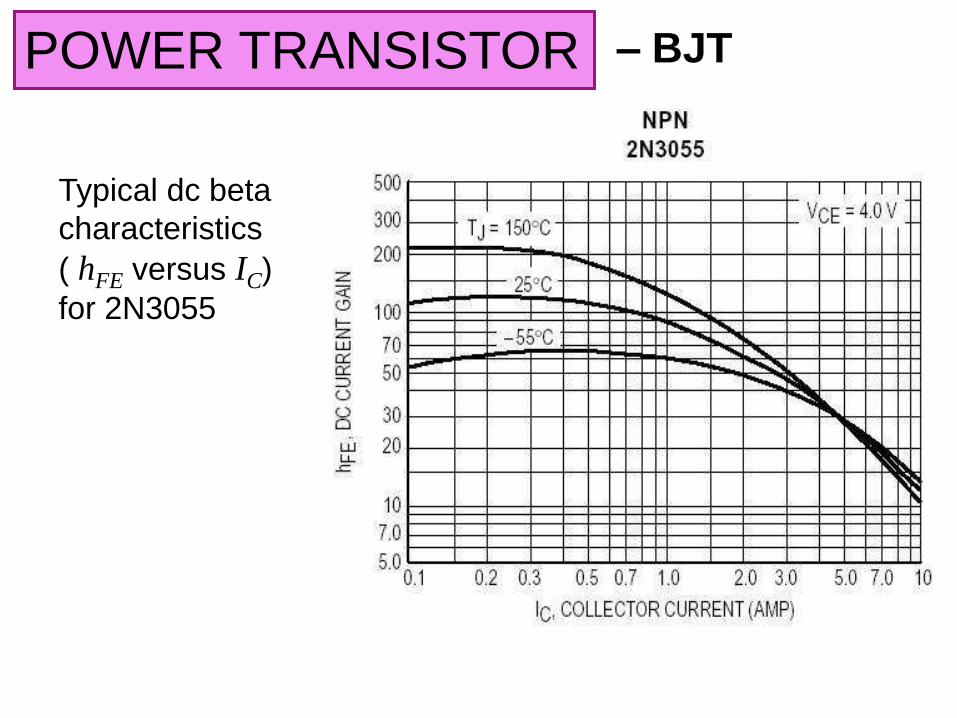
Typical dc beta
characteristics
( hFE versus IC)
for 2N3055
– BJT POWER TRANSISTOR
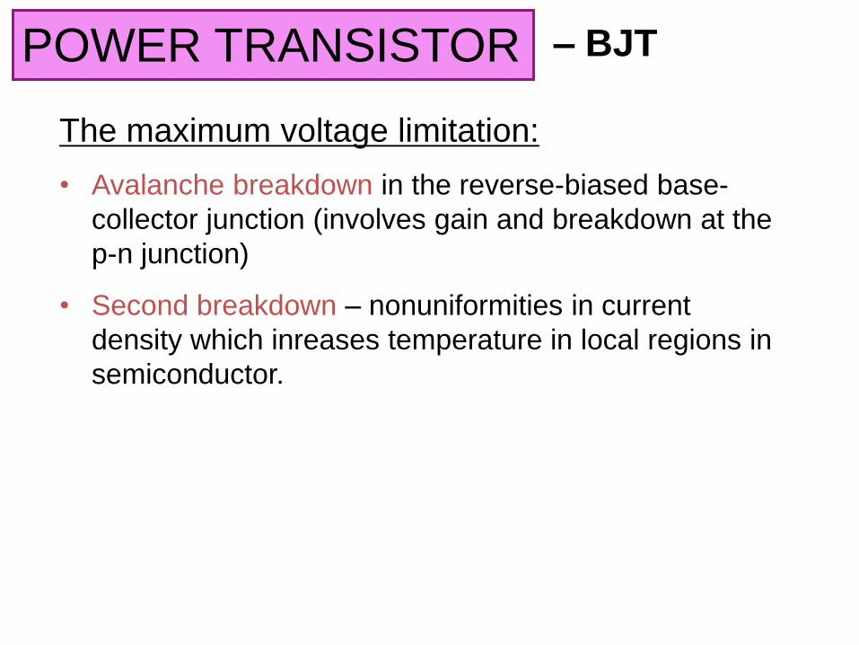
The maximum voltage limitation:
• Avalanche breakdown in the reverse-biased base-
collector junction (involves gain and breakdown at the
p-n junction)
• Second breakdown – nonuniformities in current
density which inreases temperature in local regions in
semiconductor.
– BJT POWER TRANSISTOR
Avalanche Breakdown (Figure 1)
• In Figure 1, the breakdown voltage when the base
terminal is open-circuited (IB=0) is VCEO, approx. 130V
(Figure 1).
• All the curves tend to merge to the same collector-
emitter voltage, denoted as VCE(sus) once breakdown
has occurred.
• VCE(sus) is the voltage necessary to sustain the
transistor in breakdown.
• In Figure 1, VCE(sus) is approx. 115V
– BJT POWER TRANSISTOR
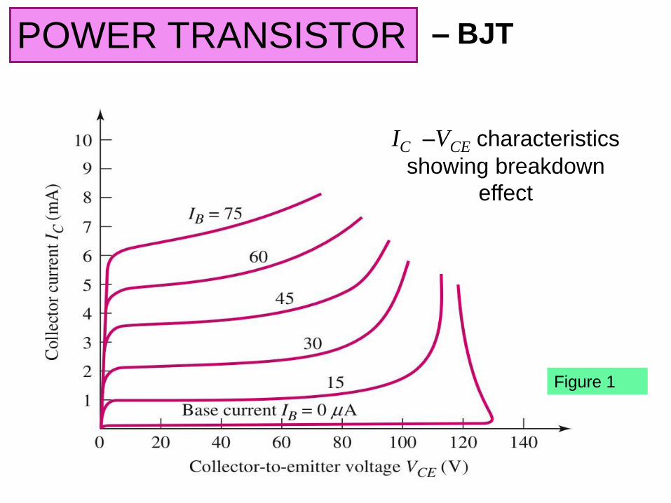
– BJT POWER TRANSISTOR
IC –VCE characteristics
showing breakdown
effect
Figure 1

– BJT POWER TRANSISTOR
BBECCEQ ivivp
The second term is usually small, hence;
CCEQ ivp
The average power over ONE CYCLE of the signal:
T
CCEQ dtivT
P0
1
The total instantaneous power dissipation in transistor
– BJT POWER TRANSISTOR
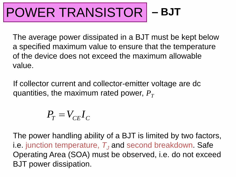
The average power dissipated in a BJT must be kept below
a specified maximum value to ensure that the temperature
of the device does not exceed the maximum allowable
value.
If collector current and collector-emitter voltage are dc
quantities, the maximum rated power, PT
CCET IVP
The power handling ability of a BJT is limited by two factors,
i.e. junction temperature, TJ and second breakdown. Safe
Operating Area (SOA) must be observed, i.e. do not exceed
BJT power dissipation.
– BJT POWER TRANSISTOR
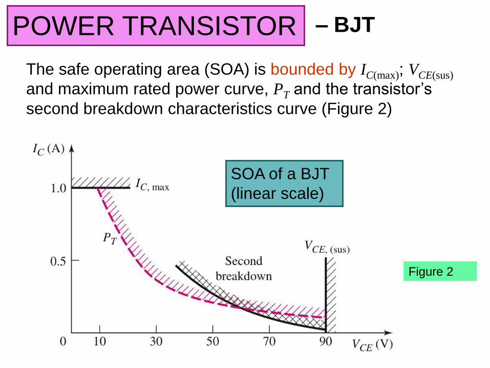
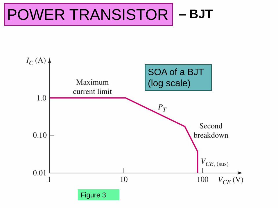
The safe operating area (SOA) is bounded by IC(max); VCE(sus)
and maximum rated power curve, PT and the transistor’s
second breakdown characteristics curve (Figure 2)
SOA of a BJT
(linear scale)
Figure 2
– BJT POWER TRANSISTOR
SOA of a BJT
(log scale)
Figure 3
– BJT POWER TRANSISTOR
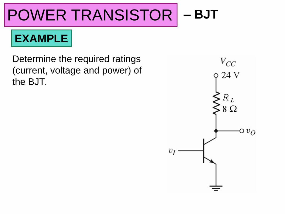
EXAMPLE
Determine the required ratings
(current, voltage and power) of
the BJT.
– BJT POWER TRANSISTOR
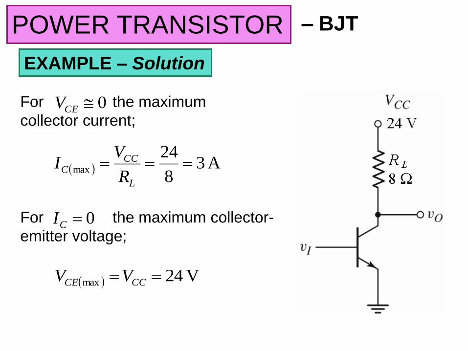
EXAMPLE – Solution
For the maximum
collector current; 0CEV
A 38
24max
L
CCC
R
VI
For the maximum collector-
emitter voltage; 0CI
V 24max CCCE VV
– BJT POWER TRANSISTOR
EXAMPLE – Solution
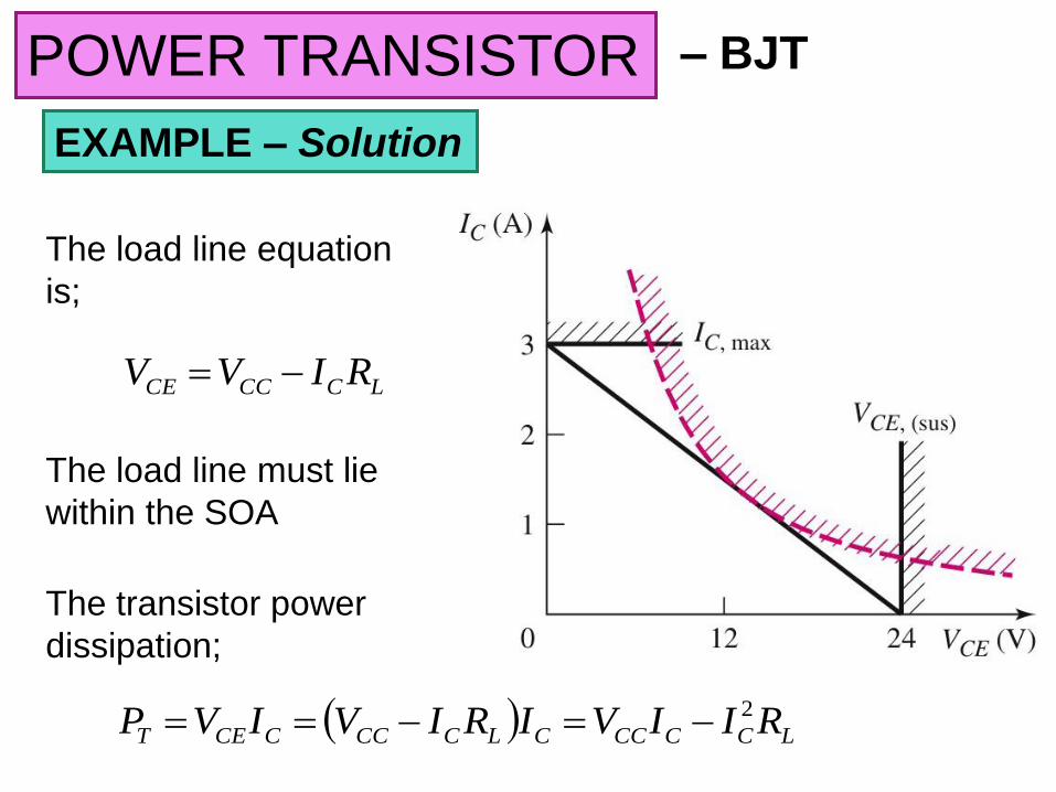
The load line equation
is;
The load line must lie
within the SOA
LCCCCE RIVV
The transistor power
dissipation;
LCCCCCLCCCCCET RIIVIRIVIVP 2
– BJT POWER TRANSISTOR
EXAMPLE – Solution
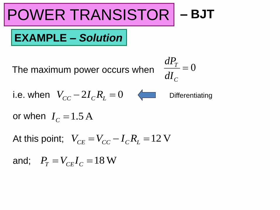
The maximum power occurs when
02 LCCC RIV
0C
T
dI
dP
i.e. when
or when A 5.1CI
At this point; V 12 LCCCCE RIVV
and; W18 CCET IVP
Differentiating
– BJT POWER TRANSISTOR
EXAMPLE – Solution
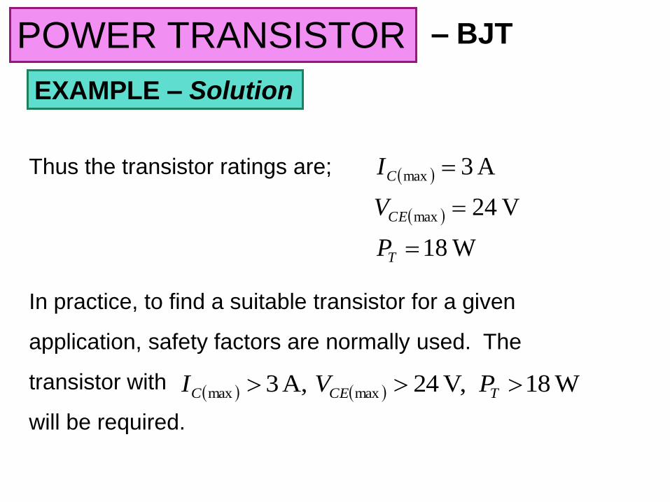
Thus the transistor ratings are;
W18
V 24
A 3
max
max
T
CE
C
P
V
I
In practice, to find a suitable transistor for a given
application, safety factors are normally used. The
transistor with
will be required.
W18 V, 24 A, 3 maxmax TCEC PVI
– BJT POWER TRANSISTOR
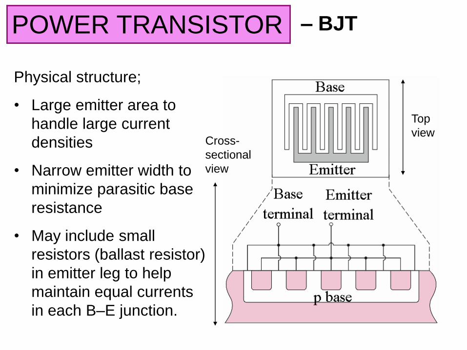
Physical structure;
• Large emitter area to
handle large current
densities
• Narrow emitter width to
minimize parasitic base
resistance
• May include small
resistors (ballast resistor)
in emitter leg to help
maintain equal currents
in each B–E junction.
Top
view Cross-
sectional
view

Revision in a different Form to previously covered material
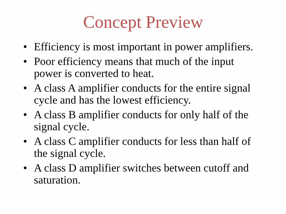
Concept Preview
• Efficiency is most important in power amplifiers.
• Poor efficiency means that much of the input power is converted to heat.
• A class A amplifier conducts for the entire signal cycle and has the lowest efficiency.
• A class B amplifier conducts for only half of the signal cycle.
• A class C amplifier conducts for less than half of the signal cycle.
• A class D amplifier switches between cutoff and saturation.

Power Amplifier
PIN Efficiency =
Input signal
POUT
POUT
PIN
Output signal
HEAT = PIN - POUT High efficiency means less heat.

Efficiency
• The dc power supplied to an amplifier is
PIN = VCC x IDC
• Efficiency = POUT/PIN x 100%
• The maximum efficiency for Class A
amplifiers with a dc collector resistance
and a separate load resistance is 25%.
• Class A is usually not acceptable when
watts of power are required.

t
IC
t
IC
t
IC
t
IC
ISAT
A B
C D
The major classes of amplifier operation
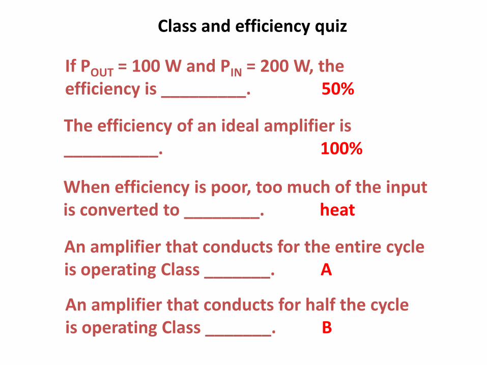
Class and efficiency quiz
If POUT = 100 W and PIN = 200 W, the efficiency is _________. 50%
The efficiency of an ideal amplifier is __________. 100%
When efficiency is poor, too much of the input is converted to ________. heat
An amplifier that conducts for the entire cycle is operating Class _______. A
An amplifier that conducts for half the cycle is operating Class _______. B
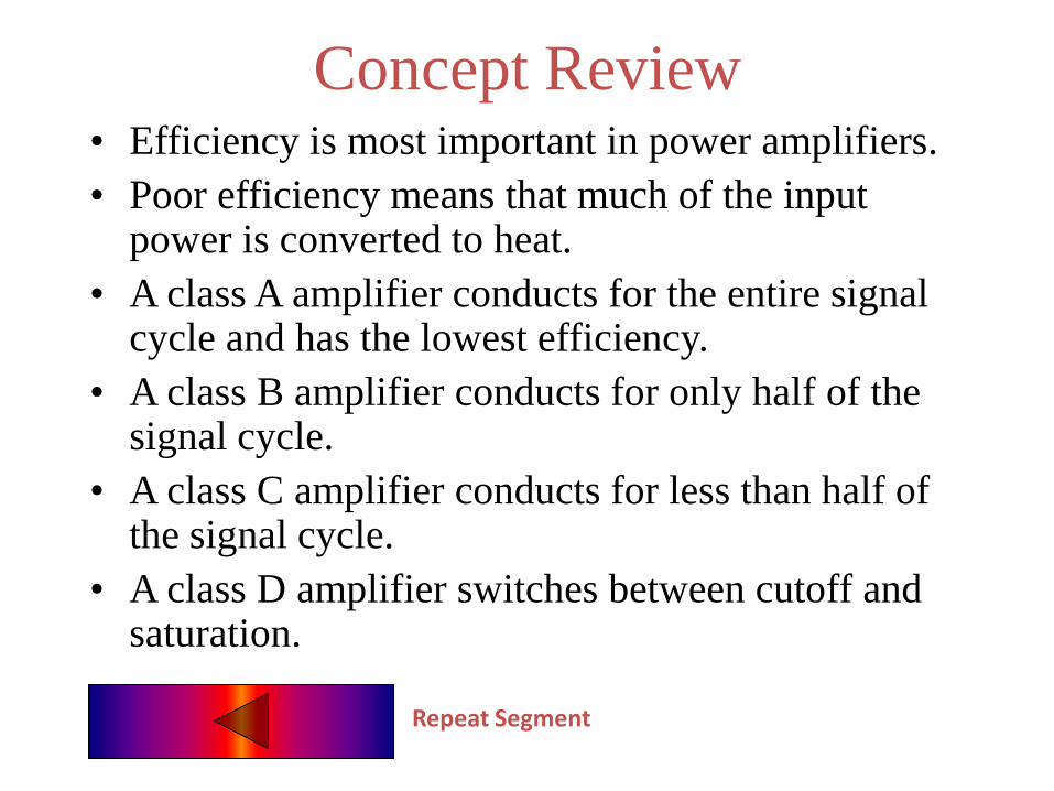
Concept Review • Efficiency is most important in power amplifiers.
• Poor efficiency means that much of the input power is converted to heat.
• A class A amplifier conducts for the entire signal cycle and has the lowest efficiency.
• A class B amplifier conducts for only half of the signal cycle.
• A class C amplifier conducts for less than half of the signal cycle.
• A class D amplifier switches between cutoff and saturation.
Repeat Segment
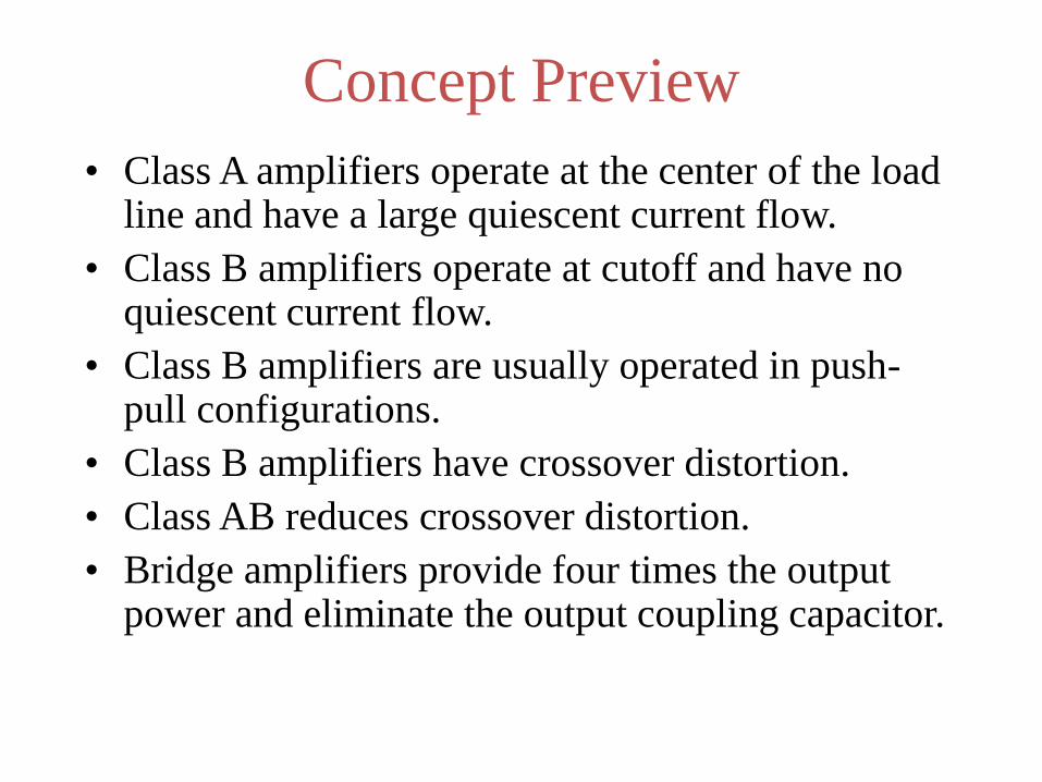
Concept Preview
• Class A amplifiers operate at the center of the load line and have a large quiescent current flow.
• Class B amplifiers operate at cutoff and have no quiescent current flow.
• Class B amplifiers are usually operated in push-pull configurations.
• Class B amplifiers have crossover distortion.
• Class AB reduces crossover distortion.
• Bridge amplifiers provide four times the output power and eliminate the output coupling capacitor.

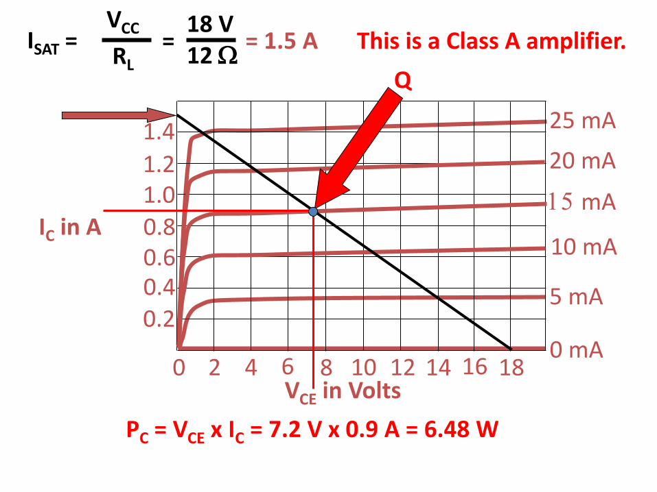
A large-signal amplifier can also be called a power amplifier.
This class A amplifier has a large quiescent collector current.
C
B E
VCC = 18 V
RL = 12 W RB = 1.2 kW
CC = 60
IB = VCC
RB
18 V
1.2 kW = = 15 mA
IC = x IB = 60 x 15 mA = 0.9 A
0 2 4 6 8 10 12 14 16 18
0.2 0.4 0.6 0.8
1.0 1.2
1.4
VCE in Volts
IC in A
5 mA
0 mA
25 mA
20 mA
15 mA
10 mA
ISAT = VCC
RL
18 V
12 W = = 1.5 A
Q
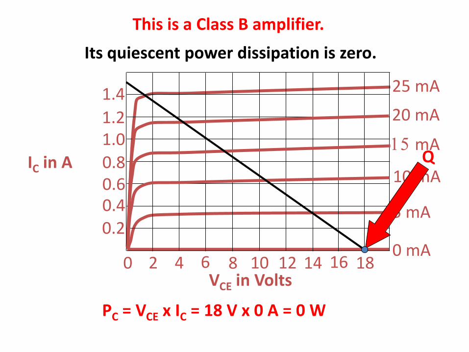
This is a Class A amplifier.
PC = VCE x IC = 7.2 V x 0.9 A = 6.48 W
0 2 4 6 8 10 12 14 16 18
0.2 0.4 0.6 0.8
1.0 1.2
1.4
VCE in Volts
IC in A
5 mA
0 mA
25 mA
20 mA
15 mA
10 mA Q
This is a Class B amplifier.
PC = VCE x IC = 18 V x 0 A = 0 W
Its quiescent power dissipation is zero.
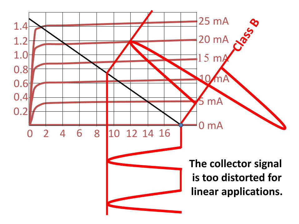
0 2 4 6 8 10 12 14 16
0.2 0.4 0.6 0.8
1.0 1.2
1.4
5 mA
0 mA
25 mA
20 mA
15 mA
10 mA
The collector signal is too distorted for linear applications.
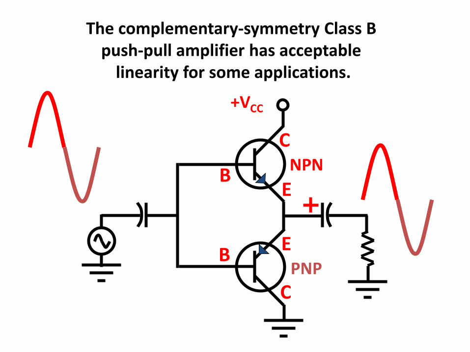
C
B
C
B E
E
+VCC
The complementary-symmetry Class B push-pull amplifier has acceptable
linearity for some applications.
NPN
PNP

NP
N
PN
P
Class B
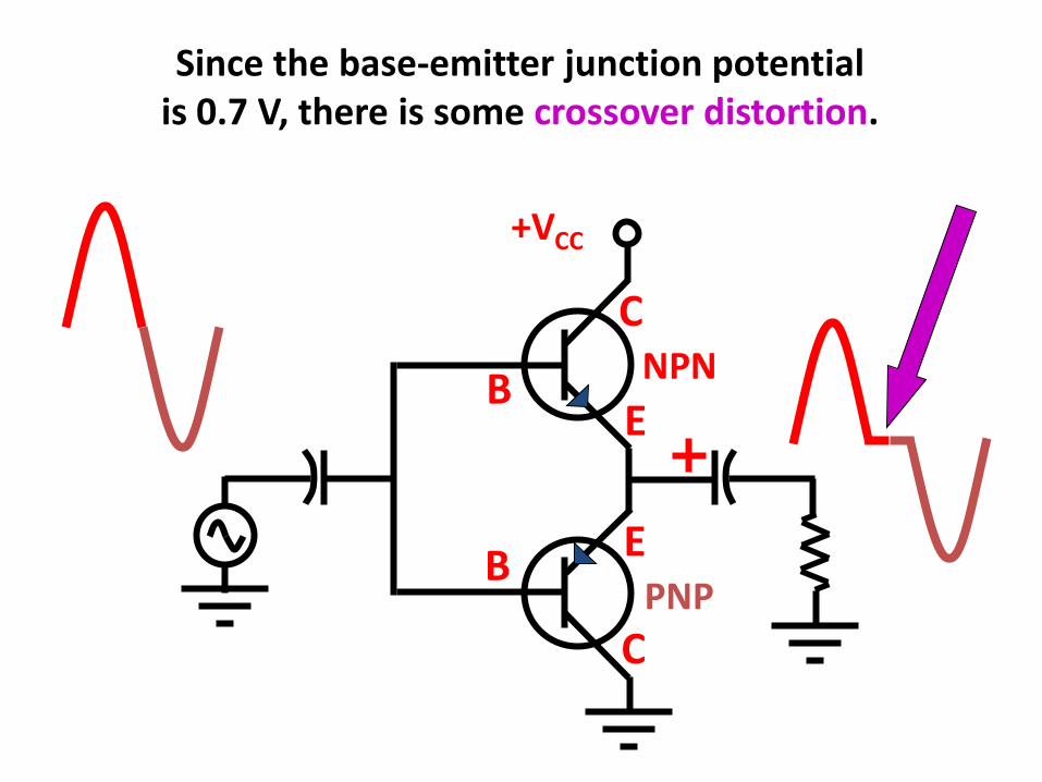
C
B
C
B E
E
+VCC
Since the base-emitter junction potential is 0.7 V, there is some crossover distortion.
NPN
PNP
C
B
C
B E
E
+VCC
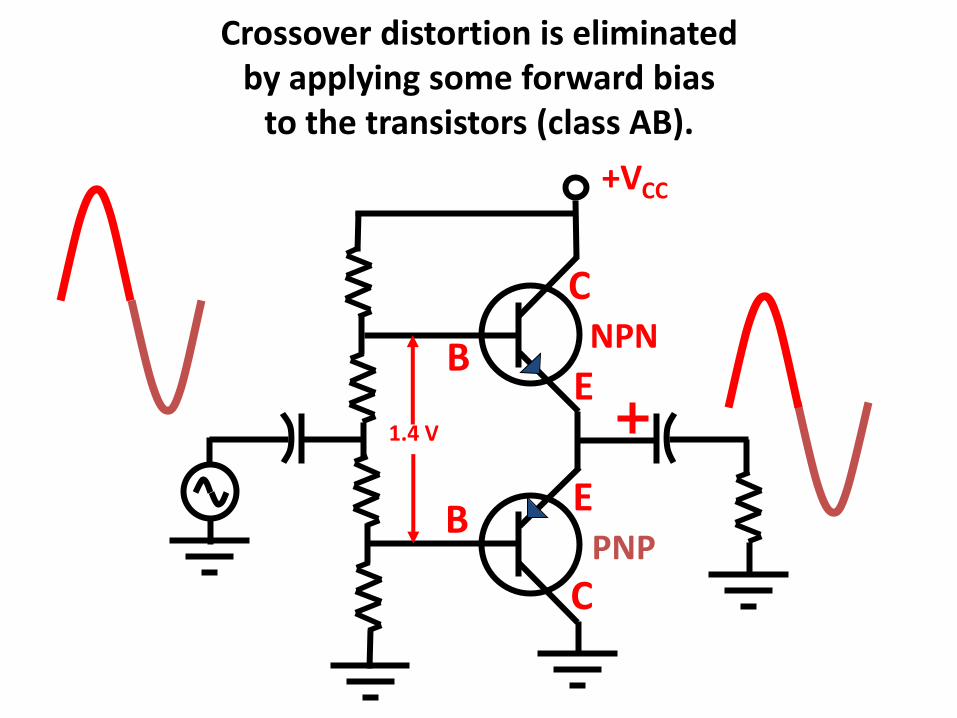
Crossover distortion is eliminated by applying some forward bias
to the transistors (class AB).
NPN
PNP
1.4 V

0 2 4 6 8 10 12 14 16 18
0.2 0.4 0.6 0.8
1.0 1.2
1.4
VCE in Volts
IC in A Q
The quiescent power dissipation is moderate for class AB.
The efficiency is much better than class A.
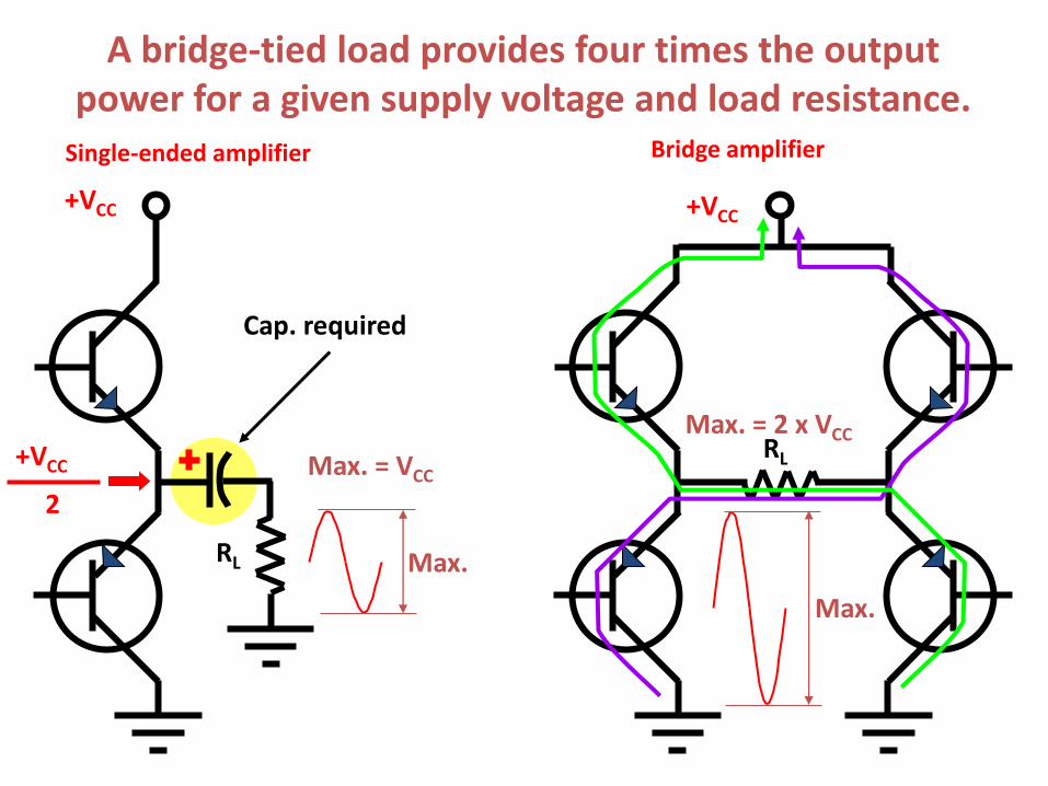
Cap. required
+VCC
RL
RL
+VCC
Single-ended amplifier
A bridge-tied load provides four times the output power for a given supply voltage and load resistance.
+VCC
2
Max.
Max. = VCC
Bridge amplifier
Max. = 2 x VCC
Max.
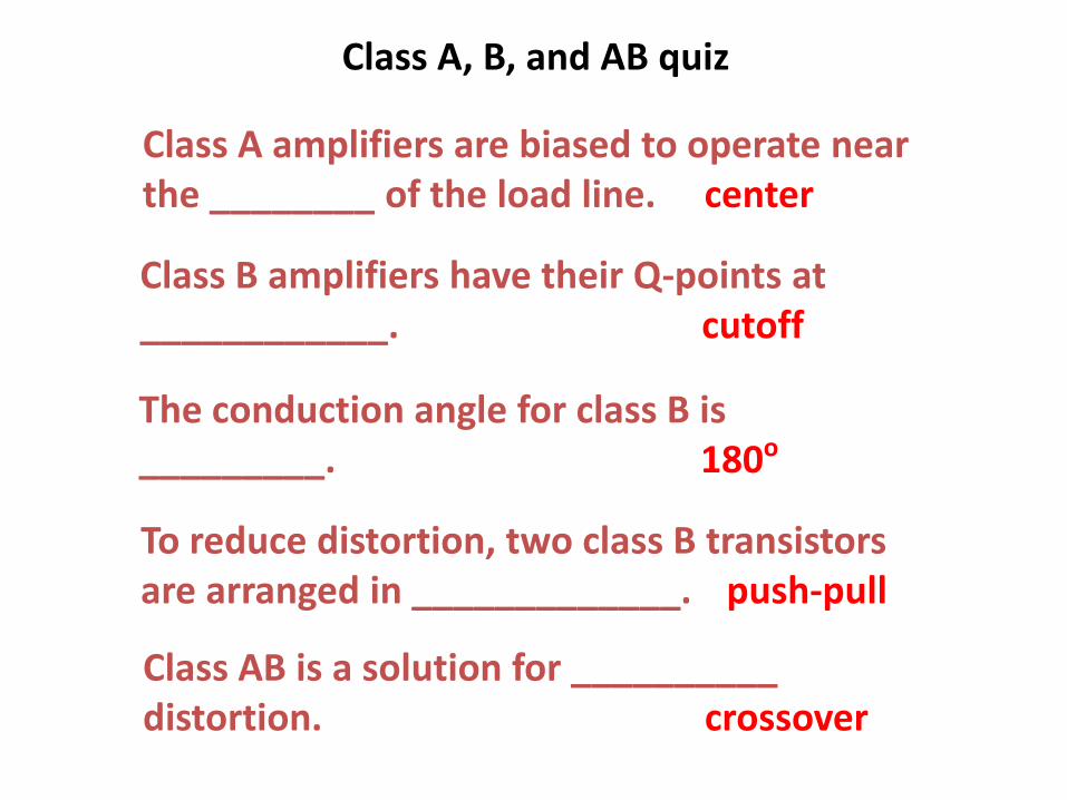
Class A, B, and AB quiz
Class A amplifiers are biased to operate near the ________ of the load line. center
Class B amplifiers have their Q-points at ____________. cutoff
The conduction angle for class B is _________. 180o
To reduce distortion, two class B transistors are arranged in _____________. push-pull
Class AB is a solution for __________ distortion. crossover
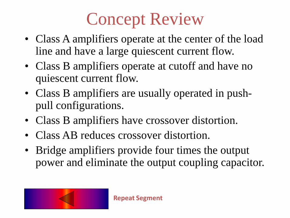
Concept Review • Class A amplifiers operate at the center of the load
line and have a large quiescent current flow.
• Class B amplifiers operate at cutoff and have no quiescent current flow.
• Class B amplifiers are usually operated in push-pull configurations.
• Class B amplifiers have crossover distortion.
• Class AB reduces crossover distortion.
• Bridge amplifiers provide four times the output power and eliminate the output coupling capacitor.
Repeat Segment
Concept Preview
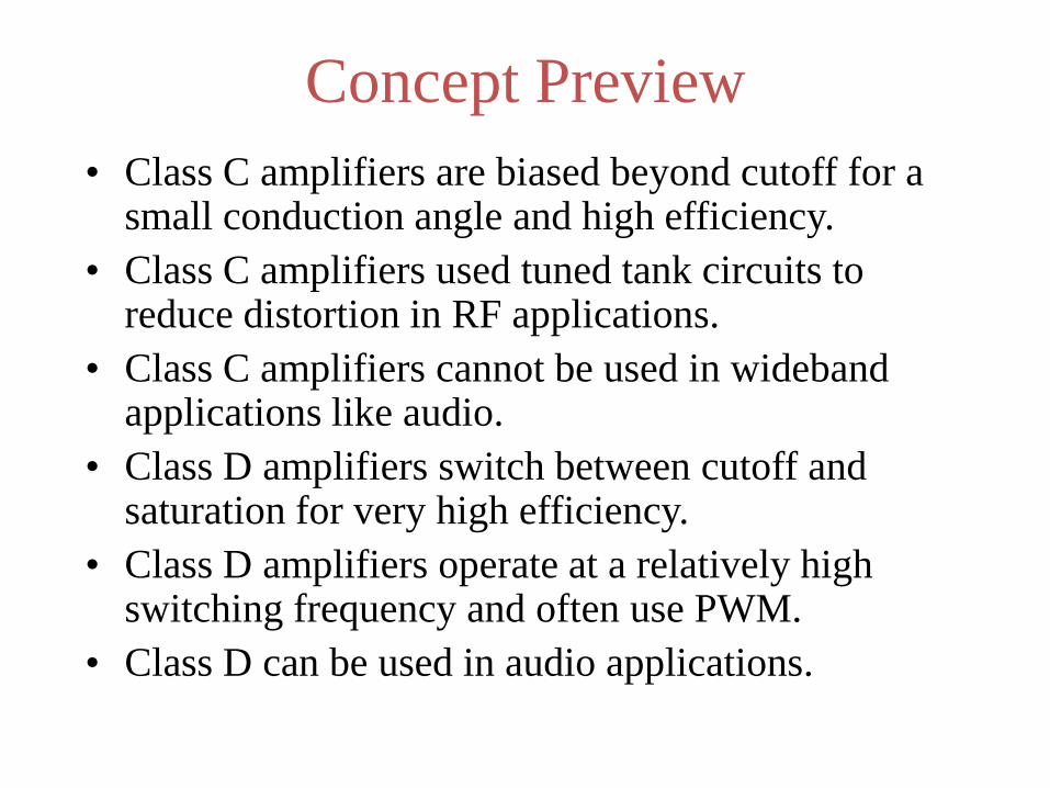
• Class C amplifiers are biased beyond cutoff for a small conduction angle and high efficiency.
• Class C amplifiers used tuned tank circuits to reduce distortion in RF applications.
• Class C amplifiers cannot be used in wideband applications like audio.
• Class D amplifiers switch between cutoff and saturation for very high efficiency.
• Class D amplifiers operate at a relatively high switching frequency and often use PWM.
• Class D can be used in audio applications.
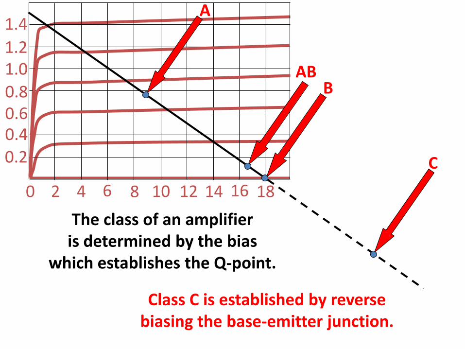
0 2 4 6 8 10 12 14 16 18
0.2 0.4 0.6 0.8
1.0 1.2
1.4 A
B
C
AB
The class of an amplifier is determined by the bias
which establishes the Q-point.
Class C is established by reverse biasing the base-emitter junction.
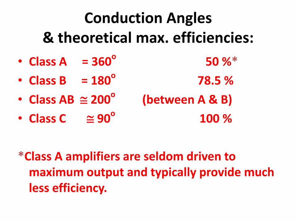
Conduction Angles & theoretical max. efficiencies:
• Class A = 360o 50 %*
• Class B = 180o 78.5 %
• Class AB 200o (between A & B)
• Class C 90o 100 %
*Class A amplifiers are seldom driven to maximum output and typically provide much less efficiency.
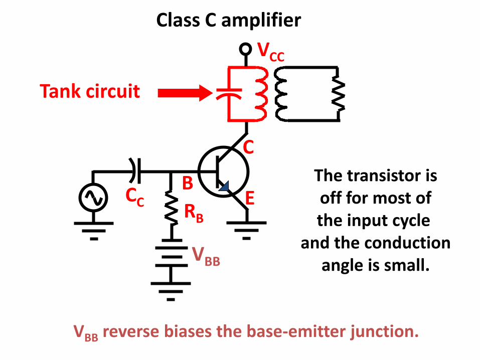
C
B E
VCC
RB CC
VBB
Class C amplifier
VBB reverse biases the base-emitter junction.
Tank circuit
The transistor is off for most of the input cycle
and the conduction angle is small.
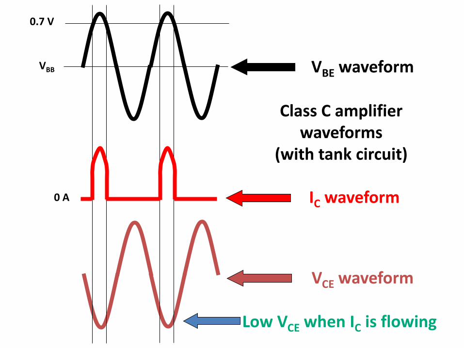
VBB
0.7 V
0 A
VBE waveform
IC waveform
VCE waveform
Class C amplifier waveforms
(with tank circuit)
Low VCE when IC is flowing
C
B E
VCC
RB CC
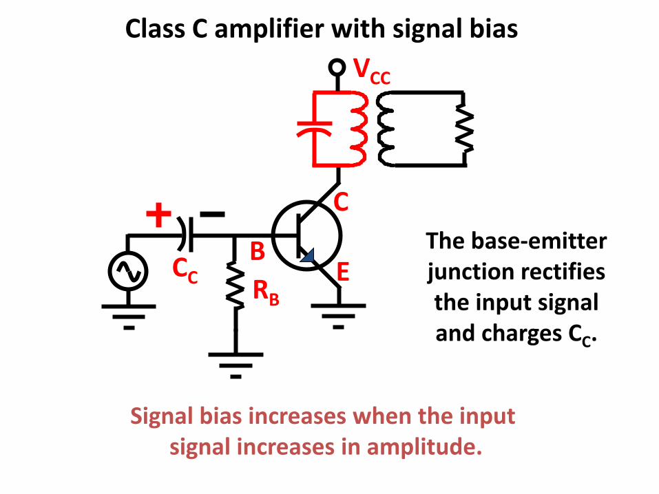
Class C amplifier with signal bias
The base-emitter junction rectifies the input signal and charges CC.
Signal bias increases when the input signal increases in amplitude.
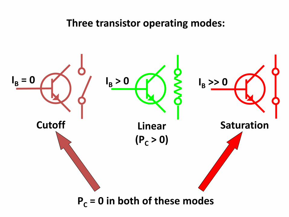
IB >> 0
Three transistor operating modes:
IB = 0 IB > 0
Cutoff Linear (PC > 0)
Saturation
PC = 0 in both of these modes
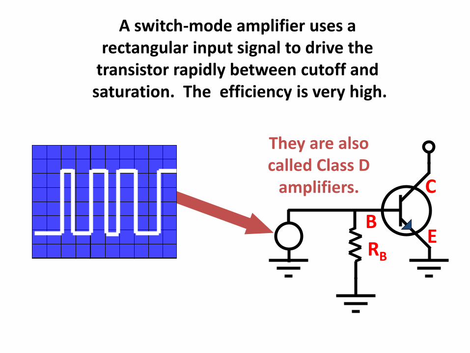
A switch-mode amplifier uses a rectangular input signal to drive the
transistor rapidly between cutoff and saturation. The efficiency is very high.
C
B E
RB
They are also called Class D
amplifiers.
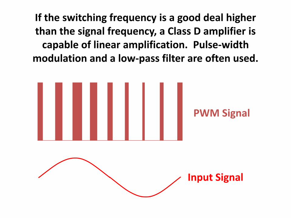
If the switching frequency is a good deal higher than the signal frequency, a Class D amplifier is
capable of linear amplification. Pulse-width modulation and a low-pass filter are often used.
PWM Signal
Input Signal
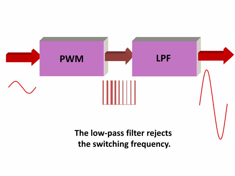
PWM LPF
The low-pass filter rejects the switching frequency.
Class C and D quiz
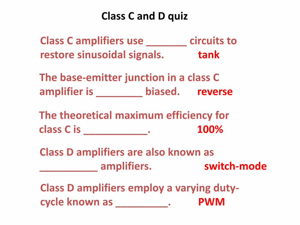
Class C amplifiers use _______ circuits to restore sinusoidal signals. tank
The base-emitter junction in a class C amplifier is ________ biased. reverse
The theoretical maximum efficiency for class C is ___________. 100%
Class D amplifiers are also known as __________ amplifiers. switch-mode
Class D amplifiers employ a varying duty- cycle known as _________. PWM
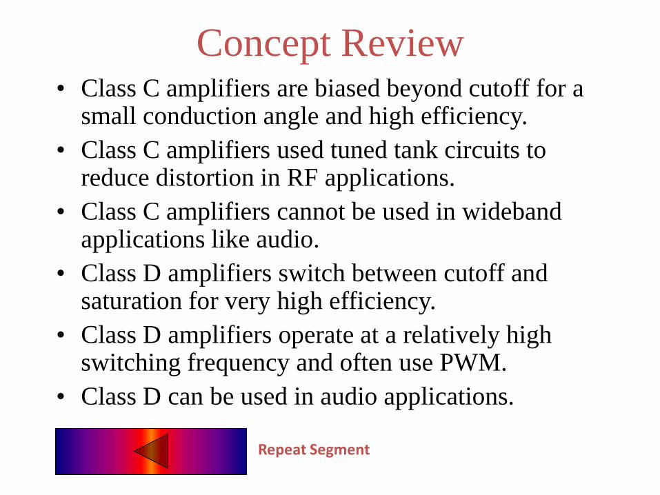
Concept Review • Class C amplifiers are biased beyond cutoff for a
small conduction angle and high efficiency.
• Class C amplifiers used tuned tank circuits to reduce distortion in RF applications.
• Class C amplifiers cannot be used in wideband applications like audio.
• Class D amplifiers switch between cutoff and saturation for very high efficiency.
• Class D amplifiers operate at a relatively high switching frequency and often use PWM.
• Class D can be used in audio applications.
Repeat Segment

More Detailed analysis as A revision
95
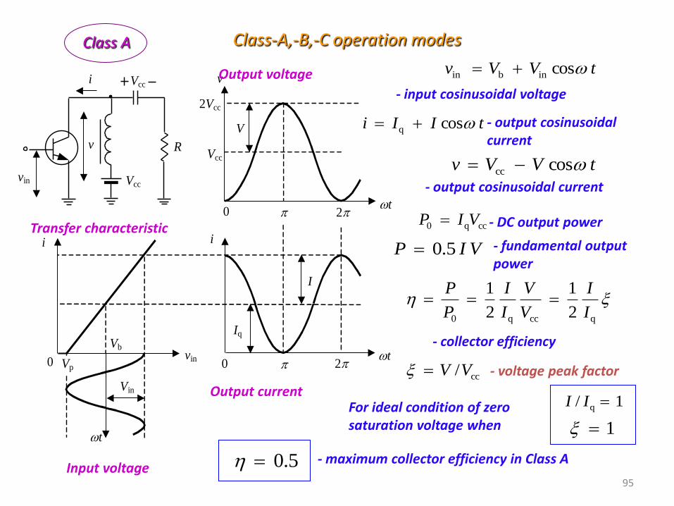
Class-A,-B,-C operation modes
Vcc
0
2Vcc
0 2
t
i v
t
I
Iq
V
R
Vcc
0
i
vin
vin
Vin
Vb
t
i
2
Vp
Vcc
v
Class A
- input cosinusoidal voltage
tVVv cos inbin
tIIi cos q
tVVv cos cc
ccq0 VIP
VIP 0.5
2
1
2
1
qccq0 I
I
V
V
I
I
P
P
cc/ VV
1 / q II
.50
- output cosinusoidal current
- output cosinusoidal current
- DC output power
- fundamental output power
Transfer characteristic
Input voltage
Output current
Output voltage
- collector efficiency
- voltage peak factor
For ideal condition of zero saturation voltage when 1
- maximum collector efficiency in Class A
96
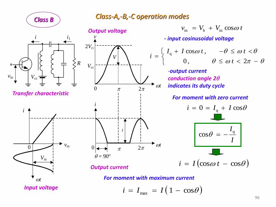
Vcc
2 0
2Vcc
t
i v
t
V R
Vcc
0
i
vin
vin
Vin
t
0 2
I
i
i1
= 90
Class-A,-B,-C operation modes
2 , 0
, cos
q
t
ttIIi
cos 0 q IIi
I
Iq cos
cos cos tIi
cos 1 max IIi
-output current conduction angle 2 indicates its duty cycle
- input cosinusoidal voltage
tVVv cos inbin
For moment with zero current
For moment with maximum current
Class B
Transfer characteristic
Output voltage
Output current
Input voltage
97
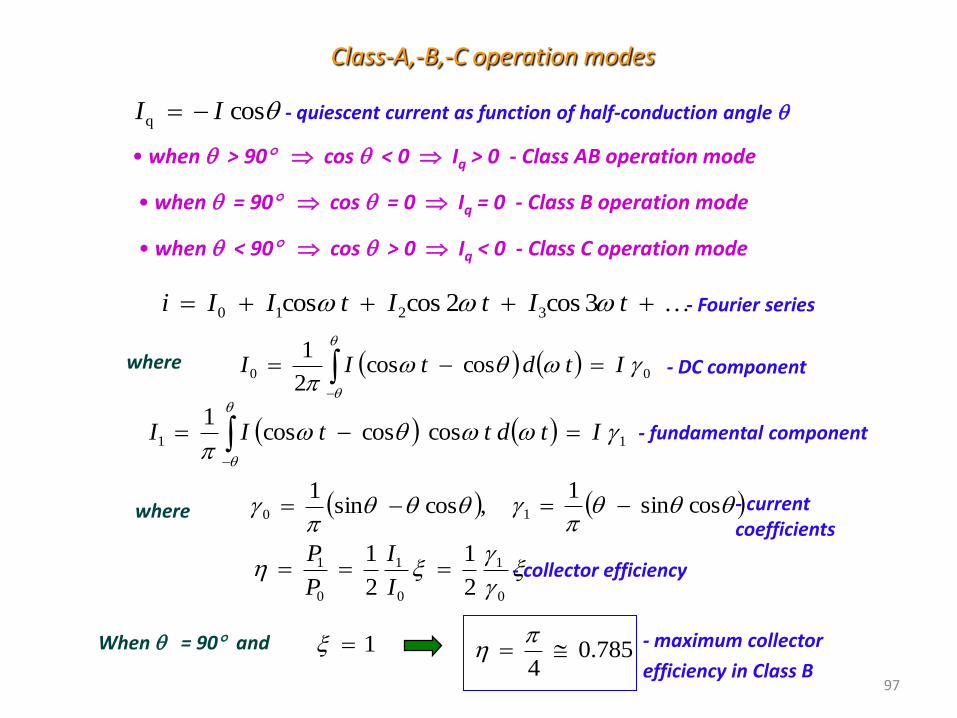
Class-A,-B,-C operation modes
- quiescent current as function of half-conduction angle
where
cos q II
• when > 90 cos < 0 Iq > 0 - Class AB operation mode
• when = 90 cos = 0 Iq = 0 - Class B operation mode
• when < 90 cos > 0 Iq < 0 - Class C operation mode
3 cos 2 cos cos 3210 tItItIIi
0 0 cos cos 2
1
ItdtII
1 1 cos cos cos 1
ItdttII
,cos sin1
0
cos sin 1
1
2
1
2
1
0
1
0
1
0
1 I
I
P
P
1 When = 90 and .7850 4
- Fourier series
where - DC component
- fundamental component
- collector efficiency
- maximum collector
efficiency in Class B
- current coefficients

98
Class-A,-B,-C operation modes
- dynamic characteristic of power amplifier or load line function within
- slope of load line
R
v
R
VIi
11
ccq
t
t 0
i
v
t
Imax
i
= 90
Vcc 2Vcc
Vsat
V
M N M' M'' N' N''
K
0
Iq
L
P
Vcos
I
RV
I
1
1
cos 1 tan
Output current
Input voltage
Transfer characteristic
99
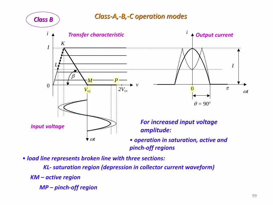
t 0
i
v
t
I
i
= 90
K
0
L
M P
Vcc 2Vcc
I
Class-A,-B,-C operation modes
For increased input voltage amplitude:
Output current
Input voltage
Transfer characteristic
Class B
MP – pinch-off region
• operation in saturation, active and pinch-off regions
KM – active region
KL- saturation region (depression in collector current waveform)
• load line represents broken line with three sections:
100
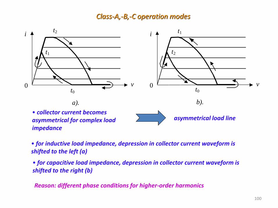
Class-A,-B,-C operation modes
• collector current becomes asymmetrical for complex load impedance
0
i
v
a).
0
i
v
b).
t0
t1
t2
t2
t1
t0
asymmetrical load line
• for inductive load impedance, depression in collector current waveform is shifted to the left (a)
• for capacitive load impedance, depression in collector current waveform is shifted to the right (b)
Reason: different phase conditions for higher-order harmonics
101
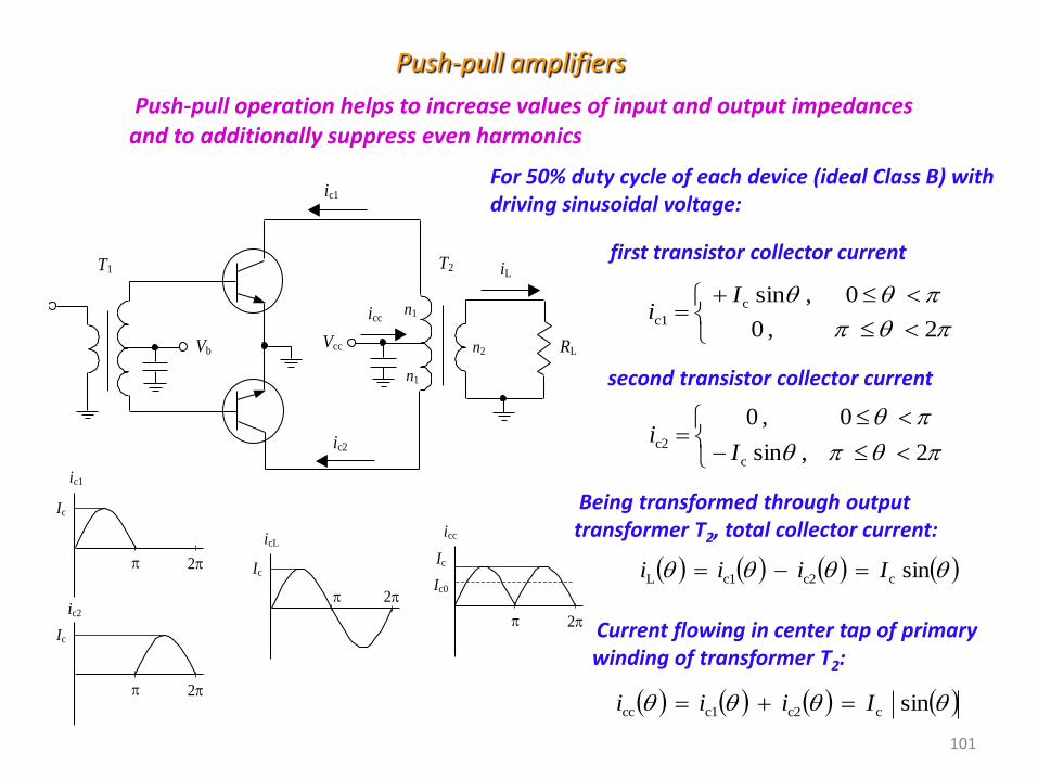
Push-pull amplifiers
Push-pull operation helps to increase values of input and output impedances and to additionally suppress even harmonics
2 , 0
0, sin c
c1
Ii
2 , sin
0, 0
c
c2I
i
first transistor collector current
second transistor collector current
RL
T1 T2
Vb Vcc
ic1
ic2
iL
icc
n2
n1
n1
Ic
2
Ic
2
Ic
2
Ic
2
Ic0
ic1
ic2
icL icc
For 50% duty cycle of each device (ideal Class B) with driving sinusoidal voltage:
Being transformed through output transformer T2, total collector current:
sin cc2c1L Iiii
Current flowing in center tap of primary winding of transformer T2:
sin cc2c1cc Iiii

102
Push-pull amplifiers
sin sin L L cL VRIv
c
2
0
ccco 2
2
1 IdiI
ccc0
2VIP
cccout2
1VIP
%5.78 4
0
out
P
P
Ideally, even-order harmonics are canceled as they are in-phase and combined in center tap of primary winding of output transformer
RL
T1 T2
Vb Vcc
ic1
ic2
iL
icc
n2
n1
n1 To eliminate losses, it is necessary to connect bypass capacitance to this center point
As for 50% duty cycle, third- and higher-order odd harmonics do not exist, ideally sinusoidal signal will appear in load
Total DC collector current
For zero saturation resistance when collector voltage amplitude Vc = Vcc and equal turns of winding when VL = Vc, DC and fundamental output powers
Maximum theoretical collector efficiency that can be achieved in Class B operation
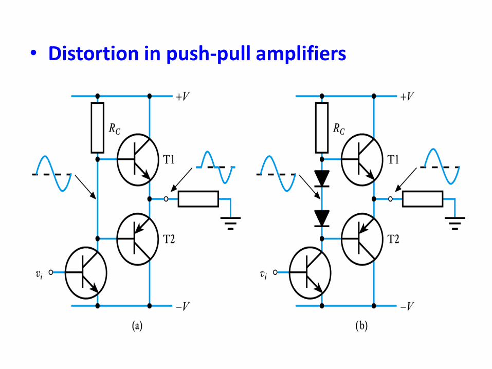
• Distortion in push-pull amplifiers
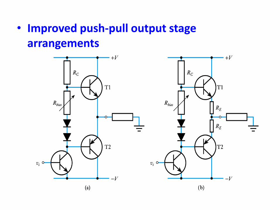
• Improved push-pull output stage arrangements
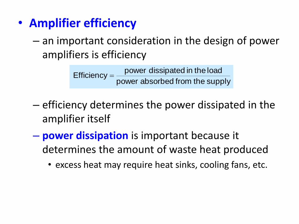
• Amplifier efficiency
– an important consideration in the design of power amplifiers is efficiency
– efficiency determines the power dissipated in the amplifier itself
– power dissipation is important because it determines the amount of waste heat produced
• excess heat may require heat sinks, cooling fans, etc.
supplythefrom absorbed power
load the indissipatedpowerEfficiency