lecture 390 – open-loop...
TRANSCRIPT

Lecture 390 – Open-Loop Comparators (4/8/02) Page 390-1
ECE 6412 - Analog Integrated Circuit Design - II © P.E. Allen - 2002
LECTURE 390 – OPEN-LOOP COMPARATORS(READING: AH – 461-475)
ObjectiveThe objective of this presentation is:1.) Show other types of continuous-time, open-loop comparators2.) Improve the performance of continuous-time, open-loop comparatorsOutline• Push-pull comparators• Comparators that can drive large capacitors• Autozeroing techniques• Comparators using hysteresis• Summary
Lecture 390 – Open-Loop Comparators (4/8/02) Page 390-2
ECE 6412 - Analog Integrated Circuit Design - II © P.E. Allen - 2002
Push-Pull ComparatorsClamped:
-
+vin
M1 M2
M3
M4
M5
M6
vout
VDD
VSS
VBias+
-
CL
M9
M8
M7
Fig. 8.3-1
Comments:• Gain reduced → Larger input resolution• Push-pull output → Higher slew rates
Lecture 390 – Open-Loop Comparators (4/8/02) Page 390-3
ECE 6412 - Analog Integrated Circuit Design - II © P.E. Allen - 2002
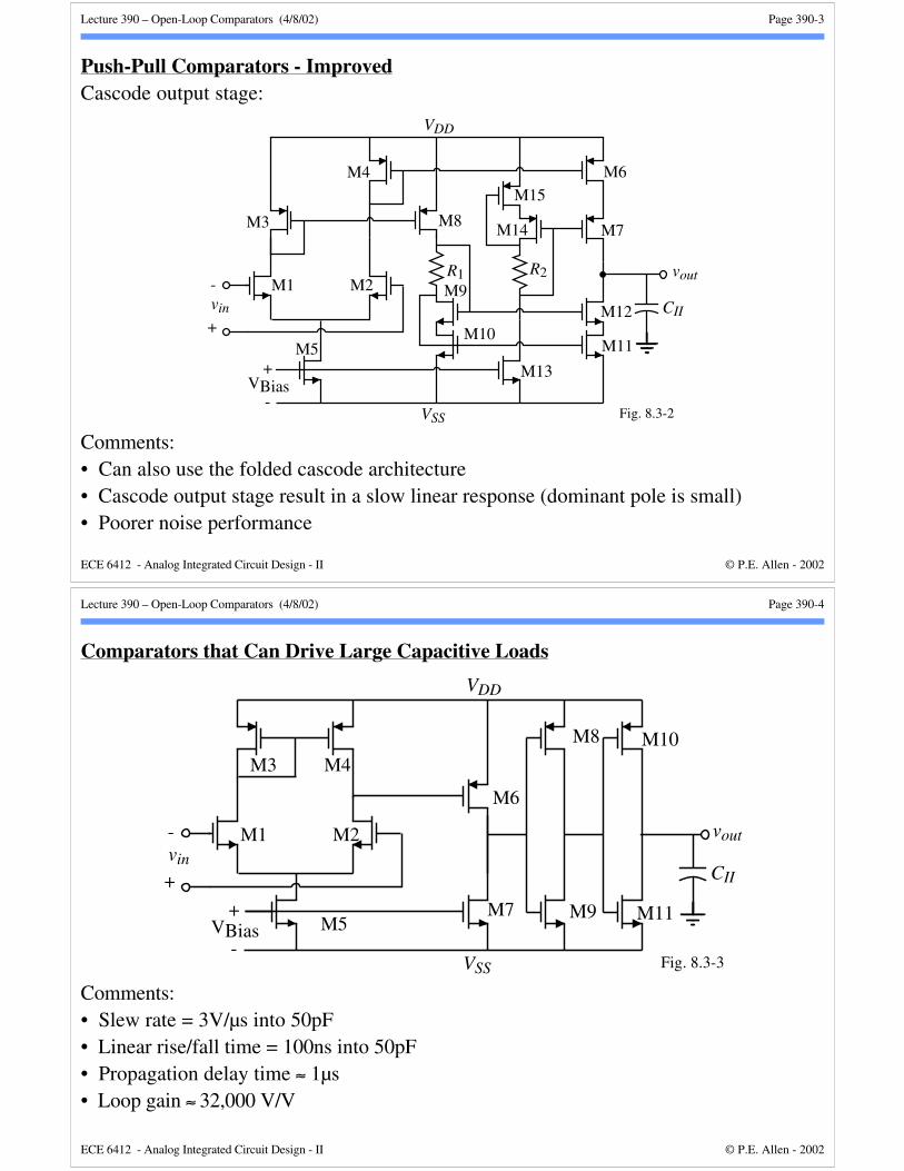
Push-Pull Comparators - ImprovedCascode output stage:
-
+vin
M1 M2
M3
M4
M5
M6
M11
vout
VDD
VSS
VBias+
-
CII
R1M9
M10
R2
M14
M15
M8
M12
M7
M13
Fig. 8.3-2
Comments:• Can also use the folded cascode architecture• Cascode output stage result in a slow linear response (dominant pole is small)• Poorer noise performance
Lecture 390 – Open-Loop Comparators (4/8/02) Page 390-4
ECE 6412 - Analog Integrated Circuit Design - II © P.E. Allen - 2002
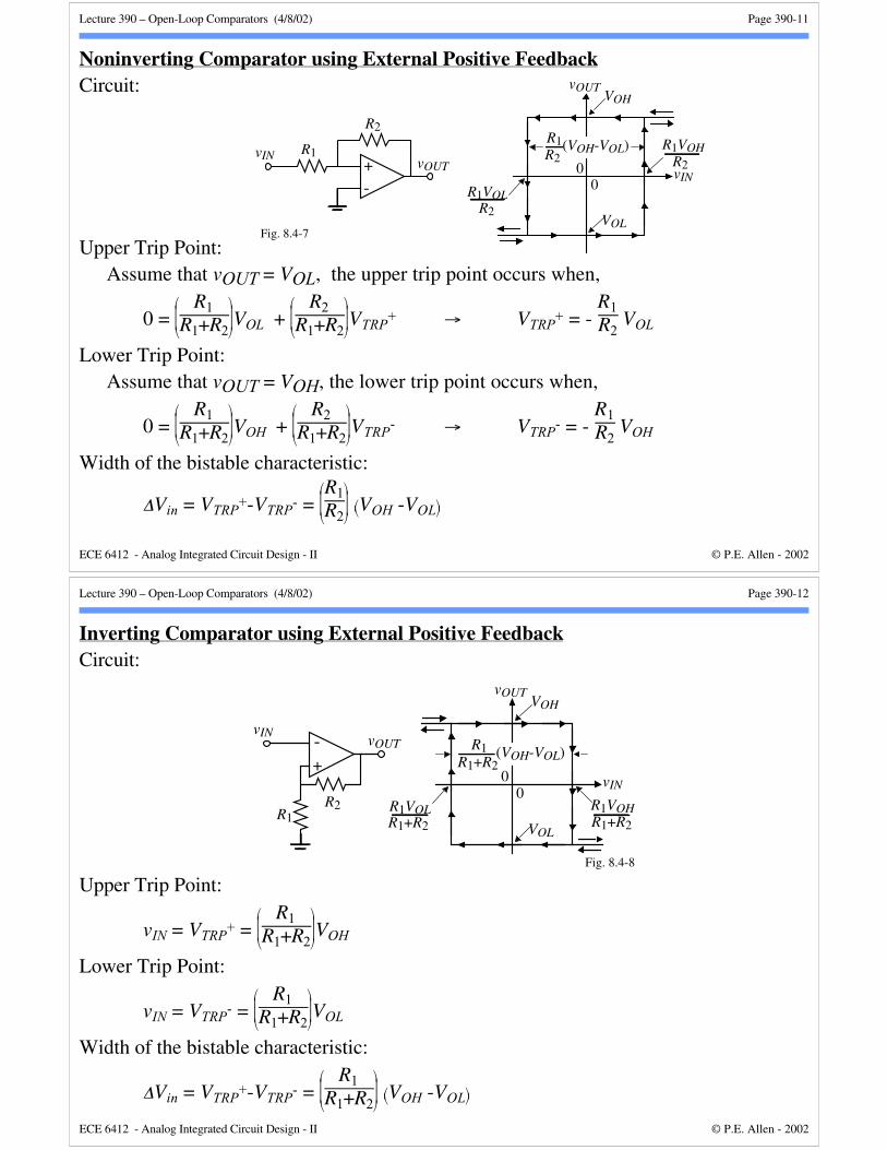
Comparators that Can Drive Large Capacitive Loads
-
+vin
M1 M2
M3 M4
M5
M6
M7
vout
VDD
VSS
VBias+
-
CII
M8
M9
M10
M11
Fig. 8.3-3
Comments:• Slew rate = 3V/µs into 50pF• Linear rise/fall time = 100ns into 50pF• Propagation delay time ≈ 1µs• Loop gain ≈ 32,000 V/V

Lecture 390 – Open-Loop Comparators (4/8/02) Page 390-5
ECE 6412 - Analog Integrated Circuit Design - II © P.E. Allen - 2002
Self-Biased Differential Amplifier†
M1 M2
M3 M4
M6
M5
VDD
VSS
vin+ vin-vout
M3 M4
M6
VDD
M1 M2
M5
VSS
vin+ vin-
VBias
VBias Extremelylarge sourcingcurrent
Fig. 8.3-4
Advantage:Large sink or source current with out a large quiescent current.
Disadvantage:
Poor common mode range (vin+ slower than vin-)
† M. Bazes, “Two Novel Full Complementary Self-Biased CMOS Differential Amplifiers,” IEEE Journal of Solid-State Circuits, Vol. 26, No. 2, Feb.1991, pp. 165-168.
Lecture 390 – Open-Loop Comparators (4/8/02) Page 390-6
ECE 6412 - Analog Integrated Circuit Design - II © P.E. Allen - 2002
Autozeroing TechniquesUse the comparator as an op amp to sample the dc input offset voltage and cancel theoffset during operation.
+-
VOS VOS+
-
IdealComparator
+-
VOS
IdealComparator
CAZ VOS+
-
+-
VOS
IdealComparator
CAZ
vIN vOUT
Model of Comparator. Autozero Cycle Comparison CycleFig. 8.4-1
Comments:• The comparator must be stable in the unity-gain mode (self-compensating comparators
are good, the two-stage op comparator would require compensation to be switched induring the autozero cycle.)
• Complete offset cancellation is limited by charge injection

Lecture 390 – Open-Loop Comparators (4/8/02) Page 390-7
ECE 6412 - Analog Integrated Circuit Design - II © P.E. Allen - 2002
Differential Implementation of Autozeroed Comparators
VOS+
-
+-
VOS
IdealComparator
CAZ
vIN-
vOUTφ1
φ1
φ1
φ2 +-
VOS
vOUT = VOS
VOS+ -
+-
VOS
Comparator during φ1 phase
Comparator during φ2 phaseDifferential Autozeroed Comparator
vOUT
Fig. 8.4-2
vIN+
φ2
vIN+
vIN-
Lecture 390 – Open-Loop Comparators (4/8/02) Page 390-8
ECE 6412 - Analog Integrated Circuit Design - II © P.E. Allen - 2002
Single-Ended Autozeroed ComparatorsNoninverting:
+-φ2
φ2
φ1 CAZ
φ1
φ1vOUTvIN
Fig. 8.4-3
Inverting:
+-φ2
CAZ
φ1
φ1
vOUTvIN
Fig. 8.4-4
Comment on autozeroing:Need to be careful about noise that gets sampled onto the autozeroing capacitor and is
present on the comparison phase of the process.

Lecture 390 – Open-Loop Comparators (4/8/02) Page 390-9
ECE 6412 - Analog Integrated Circuit Design - II © P.E. Allen - 2002
Influence of Input Noise on the ComparatorComparator without hysteresis:
vin
voutVOH
VOL
Comparatorthreshold
t
t
Fig. 8.4-6A
Comparator with hysteresis:
vin
voutVOH
VOL
t
t
VTRP+
VTRP-
Fig. 8.4-6B
Lecture 390 – Open-Loop Comparators (4/8/02) Page 390-10
ECE 6412 - Analog Integrated Circuit Design - II © P.E. Allen - 2002
Use of Hysteresis for Comparators in a Noisy EnvironmentTransfer curve of a comparator with hysteresis:
vOUT
vIN
VTRP+
VTRP-
VOH
VOL
Fig. 8.4-5
vOUT
vIN
VOH
VOL
00
R1R2
(VOH-VOL) VTRP+
VTRP-
Counterclockwise Bistable Clockwise Bistable
Hysteresis is achieved by the use of positive feedback• Externally• Internally
Lecture 390 – Open-Loop Comparators (4/8/02) Page 390-11
ECE 6412 - Analog Integrated Circuit Design - II © P.E. Allen - 2002
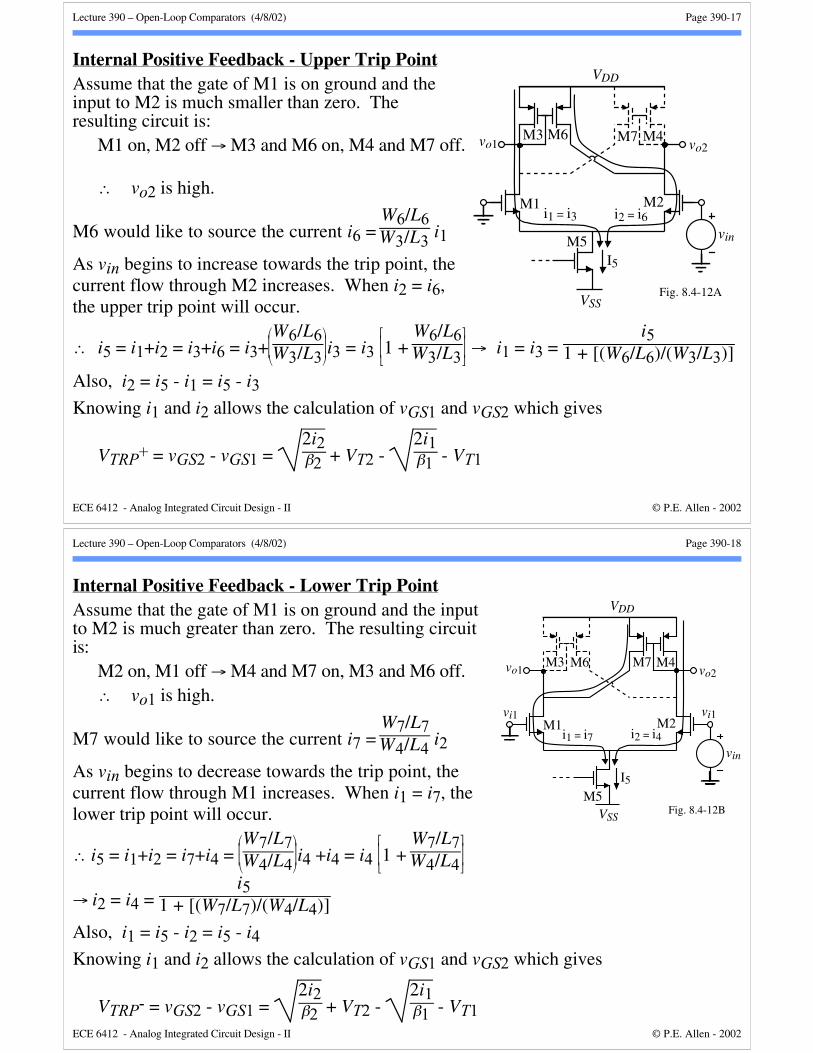
Noninverting Comparator using External Positive FeedbackCircuit:
Upper Trip Point:Assume that vOUT = VOL, the upper trip point occurs when,
0 =
R1
R1+R2VOL +
R2
R1+R2VTRP
+ → VTRP+ = -
R1R2
VOL
Lower Trip Point:Assume that vOUT = VOH, the lower trip point occurs when,
0 =
R1
R1+R2VOH +
R2
R1+R2VTRP
- → VTRP- = -
R1R2
VOH
Width of the bistable characteristic:
∆Vin = VTRP+-VTRP
- =
R1
R2 VOH -VOL
vOUT
vIN
VOH
VOL
+-
vOUTvIN R1
R2
R1VOHR2
R1VOLR2
Fig. 8.4-7
00
R1R2
(VOH-VOL)
Lecture 390 – Open-Loop Comparators (4/8/02) Page 390-12
ECE 6412 - Analog Integrated Circuit Design - II © P.E. Allen - 2002
Inverting Comparator using External Positive FeedbackCircuit:
+- vOUT
vIN
R1R2
vOUT
vIN
VOH
VOL
R1VOHR1VOL
Fig. 8.4-8
00
R1R1+R2
(VOH-VOL)
R1+R2R1+R2
Upper Trip Point:
vIN = VTRP+ =
R1
R1+R2VOH
Lower Trip Point:
vIN = VTRP- =
R1
R1+R2VOL
Width of the bistable characteristic:
∆Vin = VTRP+-VTRP
- =
R1
R1+R2 VOH -VOL

Lecture 390 – Open-Loop Comparators (4/8/02) Page 390-13
ECE 6412 - Analog Integrated Circuit Design - II © P.E. Allen - 2002
Horizontal Shifting of the CCW Bistable CharacteristicCircuit:
vOUT
vIN
VOH
VOL
+-
vOUTvIN R1
R2
R1VOHR2
Fig. 8.4-9
00
R1R2
(VOH-VOL)
VREFR1|VOL|
R2
R1+R2R2
VREF
Upper Trip Point:
VREF =
R1
R1+R2VOL +
R2
R1+R2VTRP
+ → VTRP+ =
R1+R2
R2VREF -
R1R2
VOL
Lower Trip Point:
VREF =
R1
R1+R2VOH +
R2
R1+R2VTRP
- → VTRP- =
R1+R2
R2VREF -
R1R2
VOH
Shifting Factor:
R1+R2
R2 VREF
Lecture 390 – Open-Loop Comparators (4/8/02) Page 390-14
ECE 6412 - Analog Integrated Circuit Design - II © P.E. Allen - 2002
Horizontal Shifting of the CW Bistable CharacteristicCircuit:
+- vOUT
vIN
R1R2
Fig. 8.4-10
VREF
vOUT
vIN
VOH
VOL
R1|VOL|
00
R1 (VOH-VOL)
R1VOH
R1+R2
R1VREF
R1+R2
R1+R2
R1+R2
Upper Trip Point:
vIN = VTRP+ =
R1
R1+R2VOH +
R1
R1+R2VREF
Lower Trip Point:
vIN = VTRP- =
R1
R1+R2VOL +
R1
R1+R2VREF
Shifting Factor:
R1
R1+R2 VREF

Lecture 390 – Open-Loop Comparators (4/8/02) Page 390-15
ECE 6412 - Analog Integrated Circuit Design - II © P.E. Allen - 2002
Example 8.4-1 Design of an Inverting Comparator with Hysteresis
Use the inverting bistable to design a high-gain, open-loop comparator having anupper trip point of 1V and a lower trip point of 0V if VOH = 2V and VOL = -2V.
Solution
Putting the values of this example into the above relationships gives
1 =
R1
R1+R2 2 +
R1
R1+R2VREF
and
0 =
R1
R1+R2 (-2) +
R1
R1+R2VREF
Solving these two equations gives 3R1 = R2 and VREF = 2V.
Lecture 390 – Open-Loop Comparators (4/8/02) Page 390-16
ECE 6412 - Analog Integrated Circuit Design - II © P.E. Allen - 2002
Hysteresis using Internal Positive FeedbackSimple comparator with internal positive feedback:
VSS
IBias
vo1 vo2
vi1 vi2M1 M2
M3 M4M6 M7
M5M8
VDD
Fig. 8.4-11
Lecture 390 – Open-Loop Comparators (4/8/02) Page 390-17
ECE 6412 - Analog Integrated Circuit Design - II © P.E. Allen - 2002
Internal Positive Feedback - Upper Trip PointAssume that the gate of M1 is on ground and theinput to M2 is much smaller than zero. Theresulting circuit is:
M1 on, M2 off → M3 and M6 on, M4 and M7 off.
∴ vo2 is high.
M6 would like to source the current i6 = W6/L6W3/L3 i1
As vin begins to increase towards the trip point, thecurrent flow through M2 increases. When i2 = i6,the upper trip point will occur.
∴ i5 = i1+i2 = i3+i6 = i3+
W6/L6
W3/L3 i3 = i3
1 + W6/L6W3/L3 → i1 = i3 =
i51 + [(W6/L6)/(W3/L3)]
Also, i2 = i5 - i1 = i5 - i3Knowing i1 and i2 allows the calculation of vGS1 and vGS2 which gives
VTRP+ = vGS2 - vGS1 = 2i2β2 + VT2 -
2i1β1 - VT1
VSS
vo1 vo2
M1 M2
M3 M4M6 M7
M5
VDD
Fig. 8.4-12A
I5
i1 = i3
vin
i2 = i6
Lecture 390 – Open-Loop Comparators (4/8/02) Page 390-18
ECE 6412 - Analog Integrated Circuit Design - II © P.E. Allen - 2002
Internal Positive Feedback - Lower Trip PointAssume that the gate of M1 is on ground and the inputto M2 is much greater than zero. The resulting circuitis:
M2 on, M1 off → M4 and M7 on, M3 and M6 off.∴ vo1 is high.
M7 would like to source the current i7 = W7/L7W4/L4 i2
As vin begins to decrease towards the trip point, thecurrent flow through M1 increases. When i1 = i7, thelower trip point will occur.
∴ i5 = i1+i2 = i7+i4 =
W7/L7
W4/L4 i4 +i4 = i4
1 + W7/L7W4/L4
→ i2 = i4 = i5
1 + [(W7/L7)/(W4/L4)]
Also, i1 = i5 - i2 = i5 - i4Knowing i1 and i2 allows the calculation of vGS1 and vGS2 which gives
VTRP- = vGS2 - vGS1 = 2i2β2 + VT2 -
2i1β1 - VT1
Fig. 8.4-12BVSS
vo1 vo2
vi1M1 M2
M3 M4M6 M7
M5
VDD
I5
i2 = i4
vi1
i1 = i7
vin

Lecture 390 – Open-Loop Comparators (4/8/02) Page 390-19
ECE 6412 - Analog Integrated Circuit Design - II © P.E. Allen - 2002
Example 8.4-2 - Calculation of Trip Voltages for a Comparator with Hysteresis
Consider the circuit shown. Using thetransistor device parameters given in Table3.1-2 calculate the positive and negativethreshold points if the device lengths are all 1µm and the widths are given as: W1 = W2 = W6= W7 = 10 µm and W3 = W4 = 2 µm. The gateof M1 is tied to ground and the input is thegate of M2. The current, i5 = 20 µA
Solution
To calculate the positive trip point,assume that the input has been negative and isheading positive.
i6 = (W/L)6(W/L)3
i3 = (5/1)(i3) → i3 = i5
1 + [(W/L)6/(W/L)3] = i1 = 20 µA1 + 5 = 3.33 µA
i2 = i5 − i1 = 20 − 3.33 = 16.67 µA → vGS1 =
2i1
β11/2
+VT1 =
2·3.33
(5)1101/2
+0.7 = 0.81V
vGS2 =
2i2
β21/2
+ VT2 =
2·16.67
(5)1101/2
+ 0.7 = 0.946V∴ VTRP+ ≅ vGS2−vGS1 = 0.946−0.810 = 0.136V
VSS
IBias
vo1 vo2
vi1 vi2M1 M2
M3 M4M6 M7
M5M8
VDD
Fig. 8.4-11
Lecture 390 – Open-Loop Comparators (4/8/02) Page 390-20
ECE 6412 - Analog Integrated Circuit Design - II © P.E. Allen - 2002
Example 8.4-2 - ContinuedDetermining the negative trip point, similar analysis yields
i4 = 3.33 µAi1 = 16.67 µAvGS2 = 0.81VvGS1 = 0.946VVTRP- ≅ vGS2 − vGS1 = 0.81 − 0.946 = −0.136V
PSPICE simulation results of this circuit are shown below.
1
1.2
1.4
1.6
1.8
2
2.2
2.4
2.6
-0.5 -0.4 -0.3 -0.2 -0.1 0.0 0.1 0.2 0.3 0.4 0.5
vo2
(volts)
vin (volts) Fig. 8.4-13
Lecture 390 – Open-Loop Comparators (4/8/02) Page 390-21
ECE 6412 - Analog Integrated Circuit Design - II © P.E. Allen - 2002
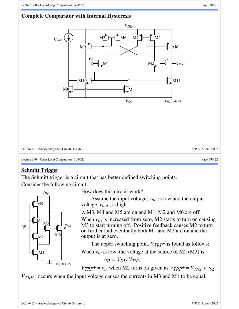
Complete Comparator with Internal Hysteresis
VSS
IBias
vout
vi1 vi2M1 M2
M3 M4M6 M7
M5M8
VDD
Fig. 8.4-14
M8M9
M10 M11
Lecture 390 – Open-Loop Comparators (4/8/02) Page 390-22
ECE 6412 - Analog Integrated Circuit Design - II © P.E. Allen - 2002
Schmitt TriggerThe Schmitt trigger is a circuit that has better defined switching points.Consider the following circuit:
How does this circuit work?Assume the input voltage, vin, is low and the output
voltage, vout , is high.
∴ M3, M4 and M5 are on and M1, M2 and M6 are off.When vin is increased from zero, M2 starts to turn on causingM3 to start turning off. Positive feedback causes M2 to turnon further and eventually both M1 and M2 are on and theoutput is at zero.
The upper switching point, VTRP+ is found as follows:
When vin is low, the voltage at the source of M2 (M3) is
vS2 = VDD-VTN3
VTRP+ = vin when M2 turns on given as VTRP+ = VTN2 + vS2
VTRP+ occurs when the input voltage causes the currents in M3 and M1 to be equal.
vin
M1
M2
M3M4
M5
M6
vout
VDD
Fig. 8.4-15
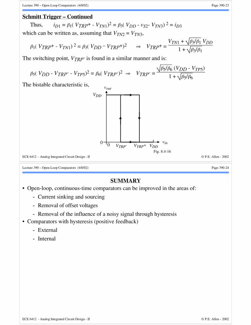
Lecture 390 – Open-Loop Comparators (4/8/02) Page 390-23
ECE 6412 - Analog Integrated Circuit Design - II © P.E. Allen - 2002
Schmitt Trigger – ContinuedThus, iD1 = β1( VTRP+ - VTN1)2 = β3( VDD - vS2- VTN3) 2 = iD3
which can be written as, assuming that VTN2 = VTN3,
β1( VTRP+ - VTN1) 2 = β3( VDD – VTRP+)2 ⇒ VTRP+ = VTN1 + β3/β1 VDD
1 + β3/β1
The switching point, VTRP- is found in a similar manner and is:
β5( VDD - VTRP- - VTP5)2 = β6( VTRP-)2 ⇒ VTRP- = β5/β6 (VDD - VTP5)
1 + β5/β6
The bistable characteristic is,
vin
vout
VDD
VDD0 0 VTRP- VTRP+
Fig. 8.4-16
Lecture 390 – Open-Loop Comparators (4/8/02) Page 390-24
ECE 6412 - Analog Integrated Circuit Design - II © P.E. Allen - 2002
SUMMARY• Open-loop, continuous-time comparators can be improved in the areas of:
- Current sinking and sourcing
- Removal of offset voltages
- Removal of the influence of a noisy signal through hysteresis• Comparators with hysteresis (positive feedback)
- External
- Internal