lecture 22: oscillator steady-state...
TRANSCRIPT
EECS 142
Lecture 22: Oscillator Steady-State Analysis
Prof. Ali M. Niknejad
University of California, Berkeley
Copyright c© 2005 by Ali M. Niknejad
A. M. Niknejad University of California, Berkeley EECS 142 Lecture 22 p. 1/23 – p. 1/23
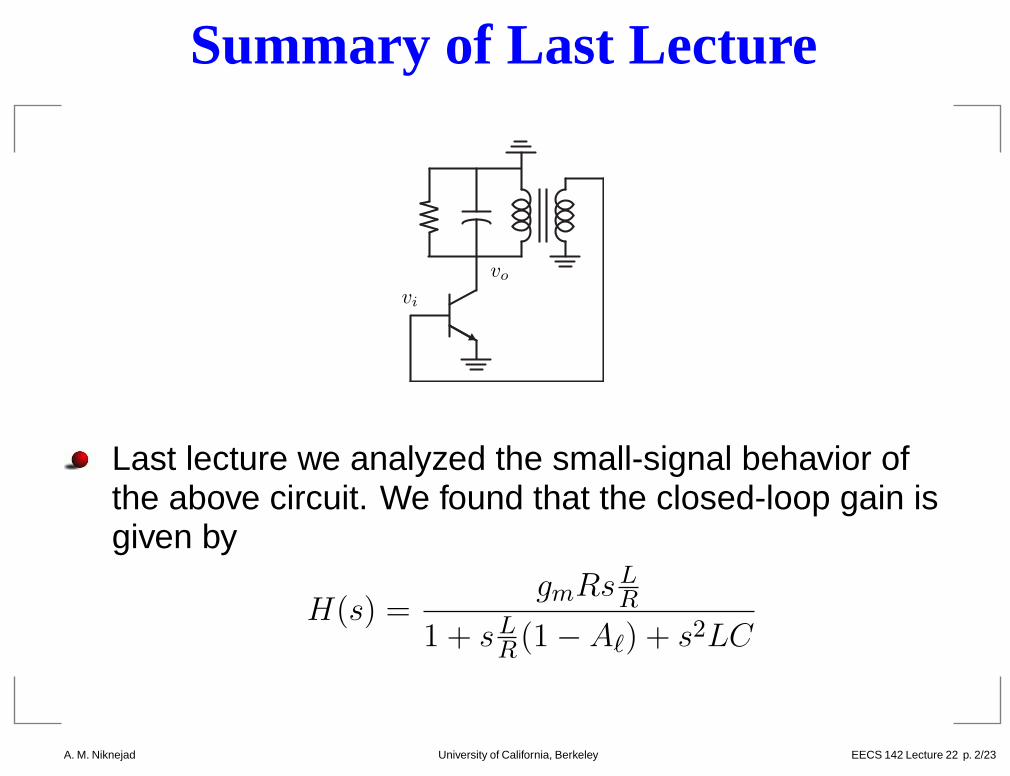
Summary of Last Lecture
vo
vi
Last lecture we analyzed the small-signal behavior ofthe above circuit. We found that the closed-loop gain isgiven by
H(s) =gmRsL
R
1 + sLR
(1 − Aℓ) + s2LC
A. M. Niknejad University of California, Berkeley EECS 142 Lecture 22 p. 2/23 – p. 2/23
Review: Role of Loop Gain
The behavior of the circuit is determined largely by Aℓ,the loop gain at DC and resonance. When Aℓ = 1, thepoles of the system are on the jω axis, correspondingto constant amplitude oscillation.
When Aℓ < 1, the circuit oscillates but decays to aquiescent steady-state.
When Aℓ > 1, the circuit begins oscillating with anamplitude which grows exponentially. Eventually, wefind that the steady state amplitude is fixed.
A. M. Niknejad University of California, Berkeley EECS 142 Lecture 22 p. 3/23 – p. 3/23
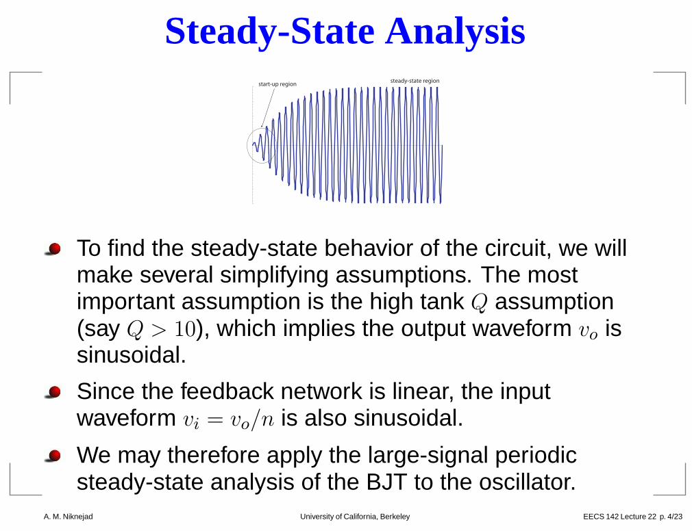
Steady-State Analysisstart-up region
steady-state region
To find the steady-state behavior of the circuit, we willmake several simplifying assumptions. The mostimportant assumption is the high tank Q assumption(say Q > 10), which implies the output waveform vo issinusoidal.
Since the feedback network is linear, the inputwaveform vi = vo/n is also sinusoidal.
We may therefore apply the large-signal periodicsteady-state analysis of the BJT to the oscillator.
A. M. Niknejad University of California, Berkeley EECS 142 Lecture 22 p. 4/23 – p. 4/23
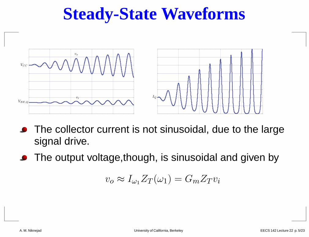
Steady-State Waveforms
vo
vi
VCC
VBE,Q
IQ
The collector current is not sinusoidal, due to the largesignal drive.
The output voltage,though, is sinusoidal and given by
vo ≈ Iω1ZT (ω1) = GmZT vi
A. M. Niknejad University of California, Berkeley EECS 142 Lecture 22 p. 5/23 – p. 5/23
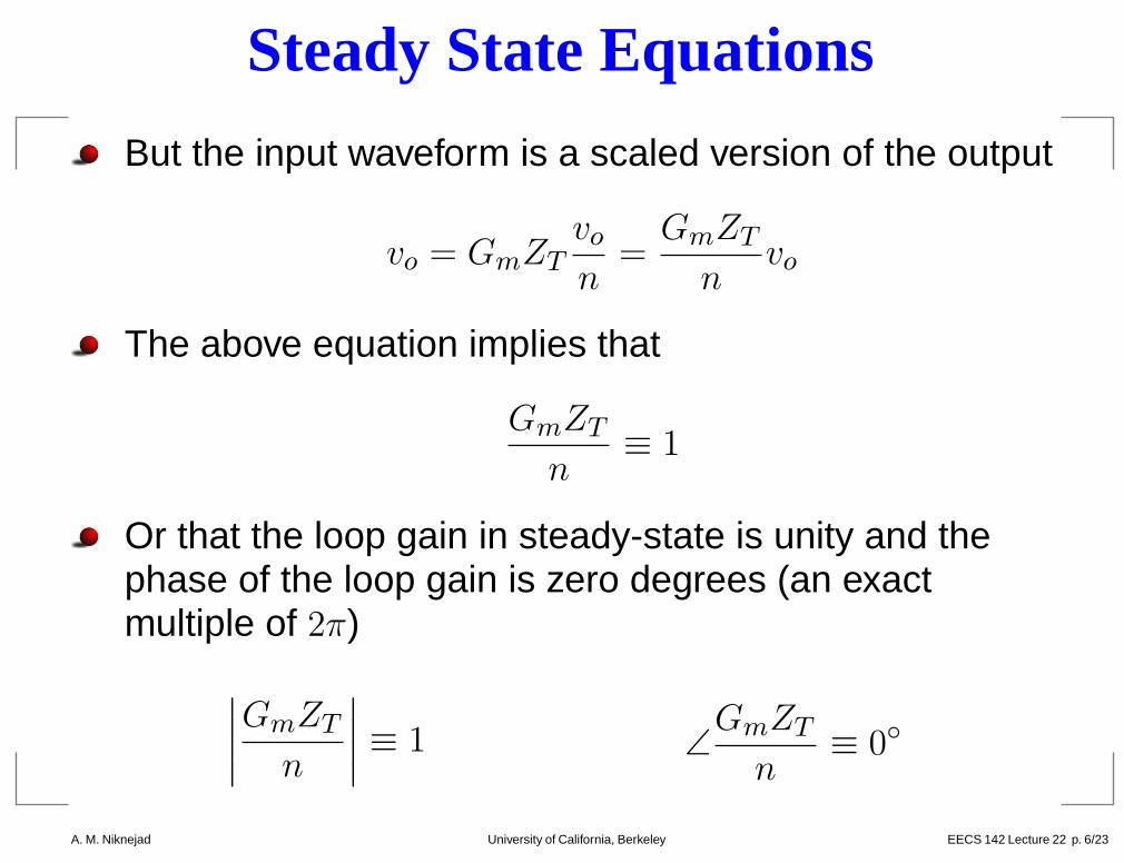
Steady State Equations
But the input waveform is a scaled version of the output
vo = GmZT
vo
n=
GmZT
nvo
The above equation implies that
GmZT
n≡ 1
Or that the loop gain in steady-state is unity and thephase of the loop gain is zero degrees (an exactmultiple of 2π)
∣
∣
∣
∣
GmZT
n
∣
∣
∣
∣
≡ 1 ∠GmZT
n≡ 0◦
A. M. Niknejad University of California, Berkeley EECS 142 Lecture 22 p. 6/23 – p. 6/23
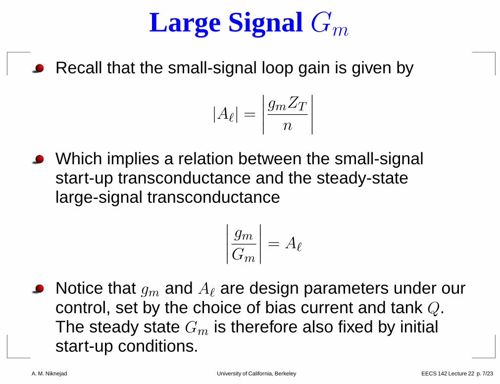
Large Signal Gm
Recall that the small-signal loop gain is given by
|Aℓ| =
∣
∣
∣
∣
gmZT
n
∣
∣
∣
∣
Which implies a relation between the small-signalstart-up transconductance and the steady-statelarge-signal transconductance
∣
∣
∣
∣
gm
Gm
∣
∣
∣
∣
= Aℓ
Notice that gm and Aℓ are design parameters under ourcontrol, set by the choice of bias current and tank Q.The steady state Gm is therefore also fixed by initialstart-up conditions.
A. M. Niknejad University of California, Berkeley EECS 142 Lecture 22 p. 7/23 – p. 7/23
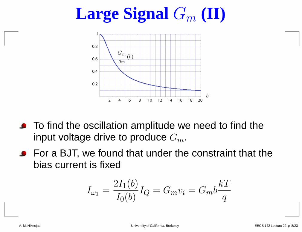
Large Signal Gm (II)
0.2
0.4
0.6
0.8
1
2 4 181614121086 20
Gm
gm
(b)
b
To find the oscillation amplitude we need to find theinput voltage drive to produce Gm.
For a BJT, we found that under the constraint that thebias current is fixed
Iω1=
2I1(b)
I0(b)IQ = Gmvi = Gmb
kT
q
A. M. Niknejad University of California, Berkeley EECS 142 Lecture 22 p. 8/23 – p. 8/23
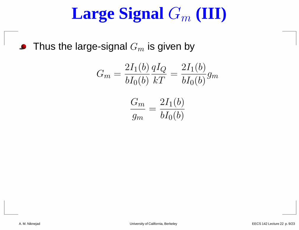
Large Signal Gm (III)
Thus the large-signal Gm is given by
Gm =2I1(b)
bI0(b)
qIQ
kT=
2I1(b)
bI0(b)gm
Gm
gm=
2I1(b)
bI0(b)
A. M. Niknejad University of California, Berkeley EECS 142 Lecture 22 p. 9/23 – p. 9/23
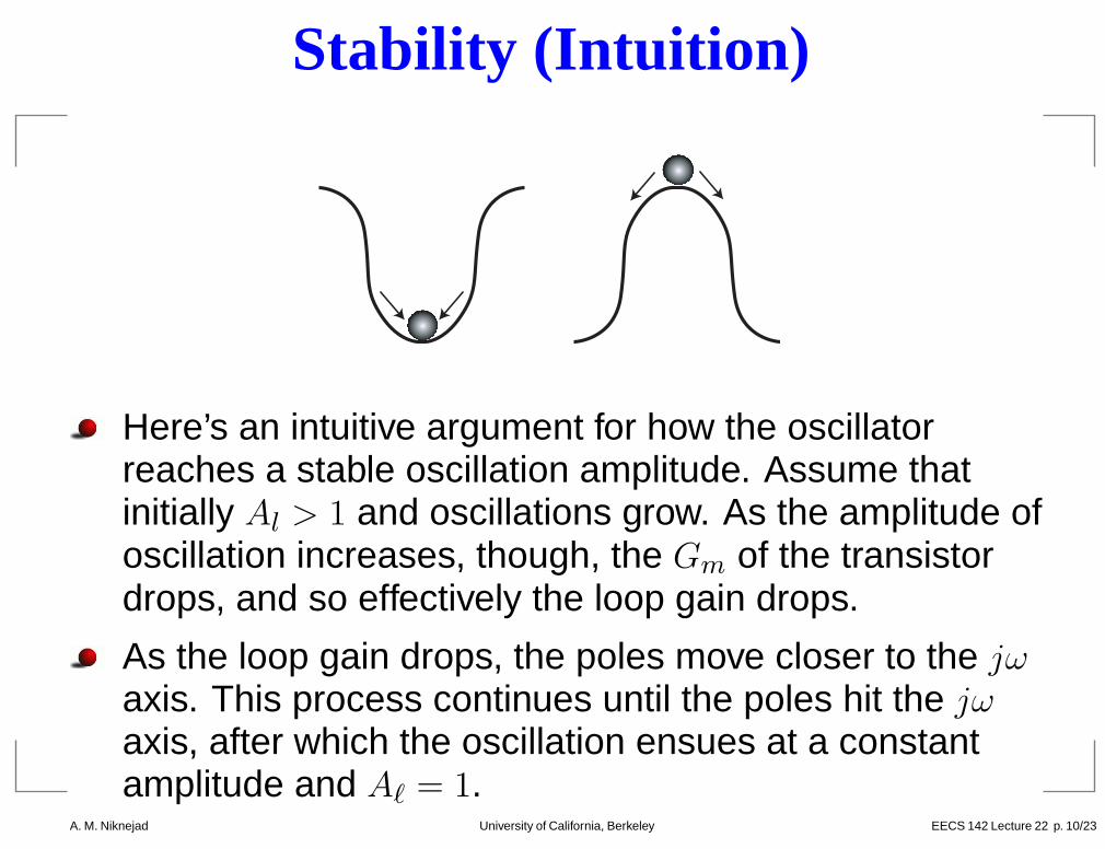
Stability (Intuition)
Here’s an intuitive argument for how the oscillatorreaches a stable oscillation amplitude. Assume thatinitially Al > 1 and oscillations grow. As the amplitude ofoscillation increases, though, the Gm of the transistordrops, and so effectively the loop gain drops.
As the loop gain drops, the poles move closer to the jωaxis. This process continues until the poles hit the jωaxis, after which the oscillation ensues at a constantamplitude and Aℓ = 1.
A. M. Niknejad University of California, Berkeley EECS 142 Lecture 22 p. 10/23 – p
Intuition (cont)
To see how this is a stable point, consider whathappens if somehow the loop gain changes. If the loopgain changes to Aℓ + |ǫ|, then we already see that thesystem will roll back. If the loop gain drops below unity,Aℓ − |ǫ|, then the poles move into the LHP andamplitude of oscillation will begin to decay.
As the oscillation amplitude decays, the Gm increasesand this causes the loop gain to grow. Thus the systemalso rolls back to the point where Aℓ = 1.
A. M. Niknejad University of California, Berkeley EECS 142 Lecture 22 p. 11/23 – p

BJT Oscillator Design
Say we desire an oscillation amplitude of v0 = 100mV ata certain oscillation frequency ω0.
We begin by selecting a loop gain Aℓ > 1 with sufficientmargin. Say Aℓ = 3.
We also tune the LC tank to ω0, being careful to includethe loaded effects of the transistor (ro, Co, Cin, Rin)
We can estimate the required first harmonic currentfrom
Iω0=
vo
R′
T
A. M. Niknejad University of California, Berkeley EECS 142 Lecture 22 p. 12/23 – p
Design (cont)
This is an estimate because the exact value of RT is notknown until we specify the operating point of thetransistor. But a good first order estimate is to neglectthe loading and use R′
T
We can now solve for the bias point from
Iω1=
2I1(b)
I0(b)IQ
b is known since it’s the oscillation amplitude normalizedto kT/q and divided by n. The above equation can besolved graphically or numerically.
Once IQ is known, we can now calculate R′′
T and iterateuntil the bias current converges to the final value.
A. M. Niknejad University of California, Berkeley EECS 142 Lecture 22 p. 13/23 – p
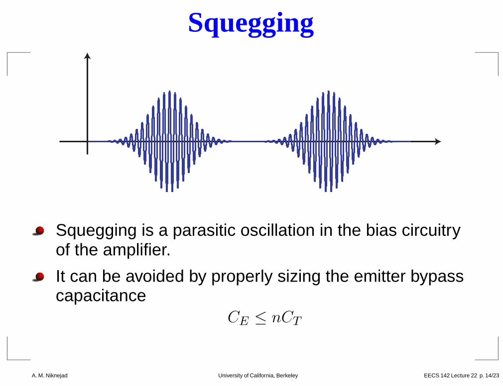
Squegging
Squegging is a parasitic oscillation in the bias circuitryof the amplifier.
It can be avoided by properly sizing the emitter bypasscapacitance
CE ≤ nCT
A. M. Niknejad University of California, Berkeley EECS 142 Lecture 22 p. 14/23 – p
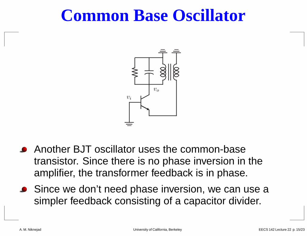
Common Base Oscillator
vo
vi
Another BJT oscillator uses the common-basetransistor. Since there is no phase inversion in theamplifier, the transformer feedback is in phase.
Since we don’t need phase inversion, we can use asimpler feedback consisting of a capacitor divider.
A. M. Niknejad University of California, Berkeley EECS 142 Lecture 22 p. 15/23 – p
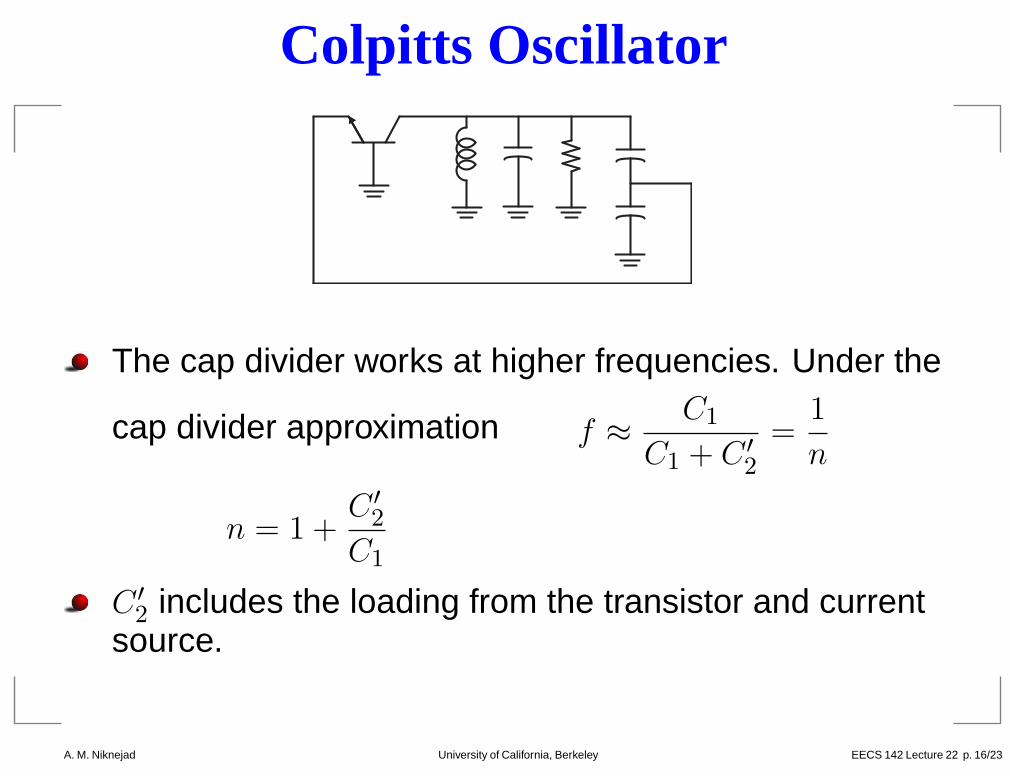
Colpitts Oscillator
The cap divider works at higher frequencies. Under the
cap divider approximation f ≈C1
C1 + C ′
2
=1
n
n = 1 +C ′
2
C1
C ′
2includes the loading from the transistor and current
source.
A. M. Niknejad University of California, Berkeley EECS 142 Lecture 22 p. 16/23 – p
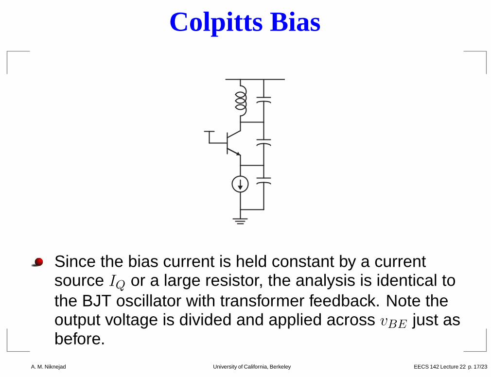
Colpitts Bias
Since the bias current is held constant by a currentsource IQ or a large resistor, the analysis is identical tothe BJT oscillator with transformer feedback. Note theoutput voltage is divided and applied across vBE just asbefore.
A. M. Niknejad University of California, Berkeley EECS 142 Lecture 22 p. 17/23 – p
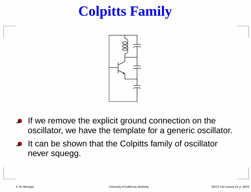
Colpitts Family
If we remove the explicit ground connection on theoscillator, we have the template for a generic oscillator.
It can be shown that the Colpitts family of oscillatornever squegg.
A. M. Niknejad University of California, Berkeley EECS 142 Lecture 22 p. 18/23 – p
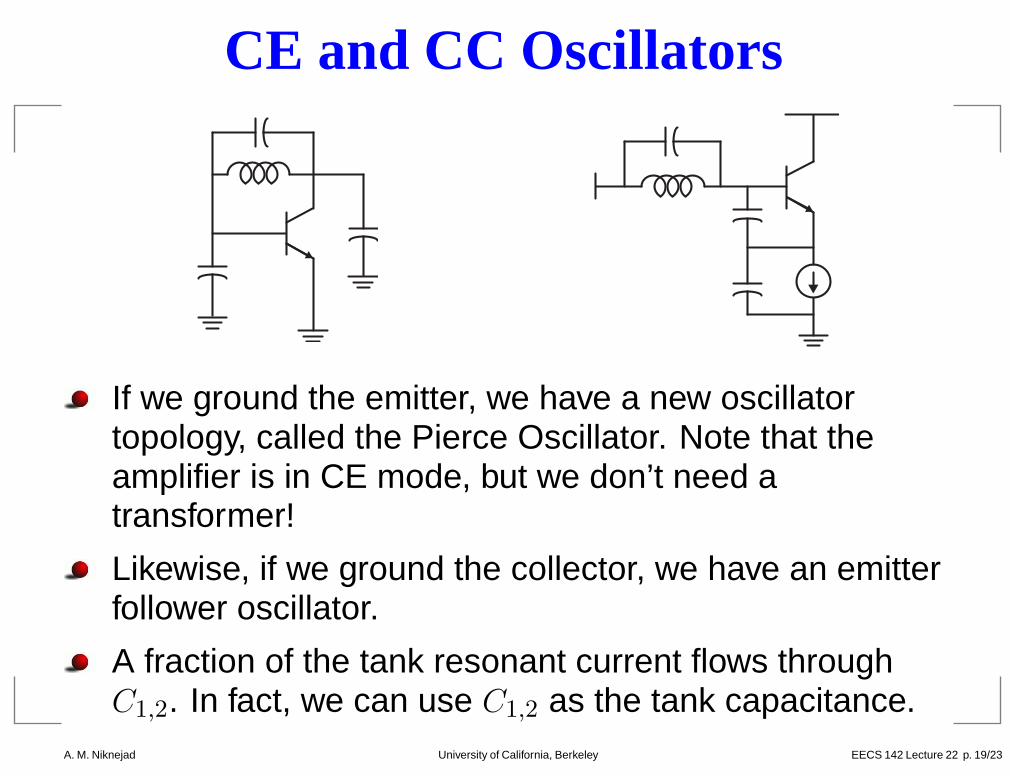
CE and CC Oscillators
If we ground the emitter, we have a new oscillatortopology, called the Pierce Oscillator. Note that theamplifier is in CE mode, but we don’t need atransformer!
Likewise, if we ground the collector, we have an emitterfollower oscillator.
A fraction of the tank resonant current flows throughC1,2. In fact, we can use C1,2 as the tank capacitance.
A. M. Niknejad University of California, Berkeley EECS 142 Lecture 22 p. 19/23 – p
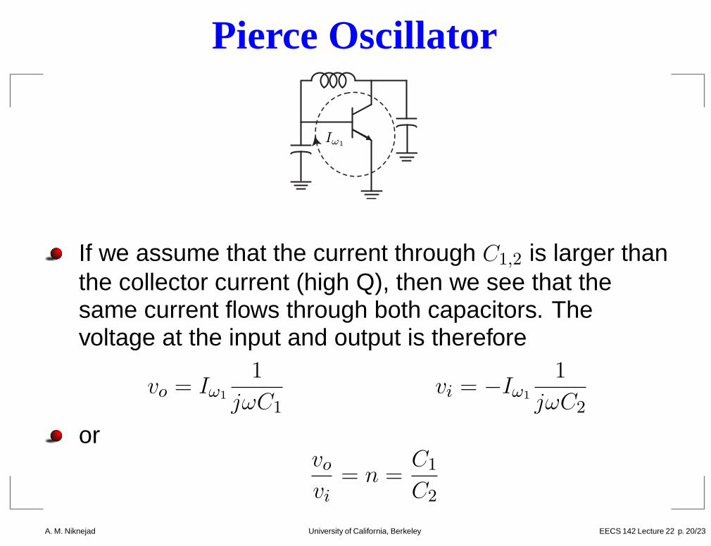
Pierce Oscillator
Iω1
If we assume that the current through C1,2 is larger thanthe collector current (high Q), then we see that thesame current flows through both capacitors. Thevoltage at the input and output is therefore
vo = Iω1
1
jωC1
vi = −Iω1
1
jωC2
orvo
vi= n =
C1
C2
A. M. Niknejad University of California, Berkeley EECS 142 Lecture 22 p. 20/23 – p
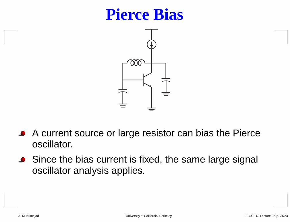
Pierce Bias
A current source or large resistor can bias the Pierceoscillator.
Since the bias current is fixed, the same large signaloscillator analysis applies.
A. M. Niknejad University of California, Berkeley EECS 142 Lecture 22 p. 21/23 – p
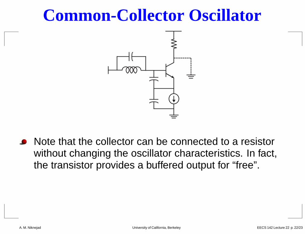
Common-Collector Oscillator
Note that the collector can be connected to a resistorwithout changing the oscillator characteristics. In fact,the transistor provides a buffered output for “free”.
A. M. Niknejad University of California, Berkeley EECS 142 Lecture 22 p. 22/23 – p
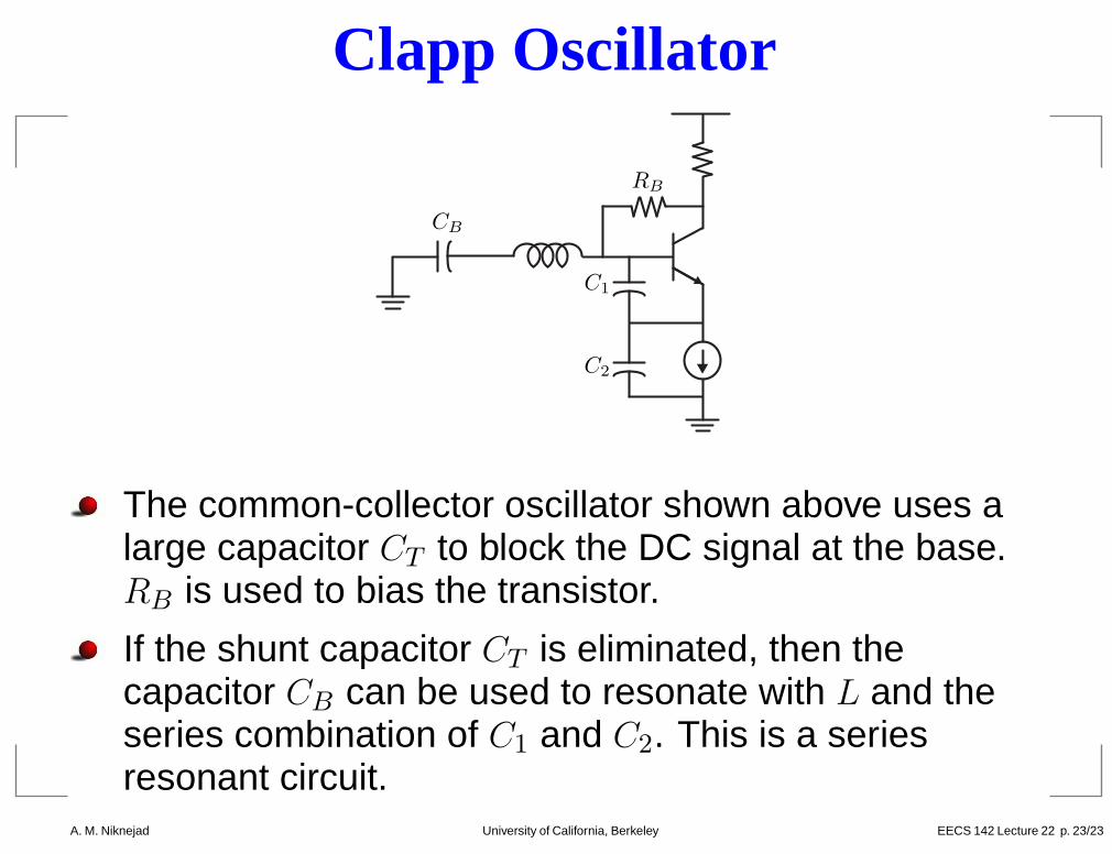
Clapp Oscillator
CB
C1
C2
RB
The common-collector oscillator shown above uses alarge capacitor CT to block the DC signal at the base.RB is used to bias the transistor.
If the shunt capacitor CT is eliminated, then thecapacitor CB can be used to resonate with L and theseries combination of C1 and C2. This is a seriesresonant circuit.
A. M. Niknejad University of California, Berkeley EECS 142 Lecture 22 p. 23/23 – p