lecture 2: scaling laws & microfabrication - engineeringmech466/mech466-lecture-2.pdf · mech...
TRANSCRIPT

1
MECH 466Microelectromechanical Systems
University of VictoriaDept. of Mechanical Engineering
Lecture 2:Scaling Laws & Microfabrication
© N. Dechev, University of Victoria
2
Scaling Laws
Microfabrication of Chips
Overview of MUMPs Microfabrication
Overview
© N. Dechev, University of Victoria

3
Scaling laws can be used to answer the question of “Why go small ?” They allow us to determine whether physical phenomena will scale more favorably or will scale poorly.
Generally, smaller things are less effected by volume dependent phenomena such as mass and inertia, and are more effected by surface area dependent phenomena such as contact forces or heat transfer.
Friction > Inertia
Heat Dissipation > Heat Storage
Electrostatic Force > Magnetic Force
Scaling Laws
© N. Dechev, University of Victoria
4
Example 1: A cube of material:
Surface Area for a cube = 6a
Volume for a cube = a
As we scale down, the value for volume will decrease more rapidly than the value for surface area. In other words, the volume/surface area ratio will decrease.
Scaling Laws
aa
a
2
3
© N. Dechev, University of Victoria

5
Assume a = 10 units
For a = 10:S.A. (surface area)V (volume)
Therefore, the ratio of
Assume a = 1 unit:S.A. (surface area)V (volume)
Therefore, the ratio
Scaling Laws
aa
a
© N. Dechev, University of Victoria
6
Assume a = 0.1 unit:S.A. (surface area)V (volume)
Therefore, the ratio
-What is the significance of this?
-Consider heat storage vs. heat dissipation.-heat storage is proportional to volume-heat dissipation is proportional to surface area
Scaling Laws
aa
a
© N. Dechev, University of Victoria

7
-Given three cubes of different sizes a = 10, 1 and 0.1, with all other properties the same, consider the ‘rate of cooling’.
-Assume that all cubes start at the same high temperature, and are allowed to cool to the same low temperature.
-The total heat contained in the smallest cube is 1,000,000 times less than the large cube.
-The total surface area (heat dissipation area) of the smallest cube is only 10,000 times less thanthe large cube.
-Therefore, there is 100 times more heat dissipation, per unit volume, in the smallest cube. In other words, it will cool at a much faster rate, even though all other conditions are the same for all cubes.
Scaling Laws
aa
a
© N. Dechev, University of Victoria
8
Example 2: What is the effect of scale, on the spring constant k of a Beam?
Step 1: Derive expression for parameter of interest
- where: k = spring constant, E = young’s modulus, w = beam width, t = beam thickness, l = beam length
Step 2: Identify all scale (i.e. length) related parameters.
- this includes w, t and l. Note that E is not a function of length.
Scaling Laws
© N. Dechev, University of Victoria

9
Step 3: Re-define all scale related parameters in terms of a single scale variable, such as L.
- Let: l = L, w = aL, and t = bL,
Step 4: Re-write expression in terms of the scale variable L:
Step 5: Simplify expression to derive relation between parameter of interest and the scale variable:
- where C = constant of proportionality, in this case:
Scaling Laws
© N. Dechev, University of Victoria
10
By simplifying, we find k is proportional to L.
In other words, as L decreases, k decreases.
Therefore, the smaller the beam, the smaller the spring constant k, or the more flexible it is.
Scaling Laws
© N. Dechev, University of Victoria
11
Example 3: What is the effect of scale, on the buoyancy force fb of a solid sphere, submersed in a liquid?
- Note: fb = (volume displaced) x (density of fluid) x g
- Volume of a sphere
-Therefore:
-Therefore:
Scaling Laws
© N. Dechev, University of Victoria
12
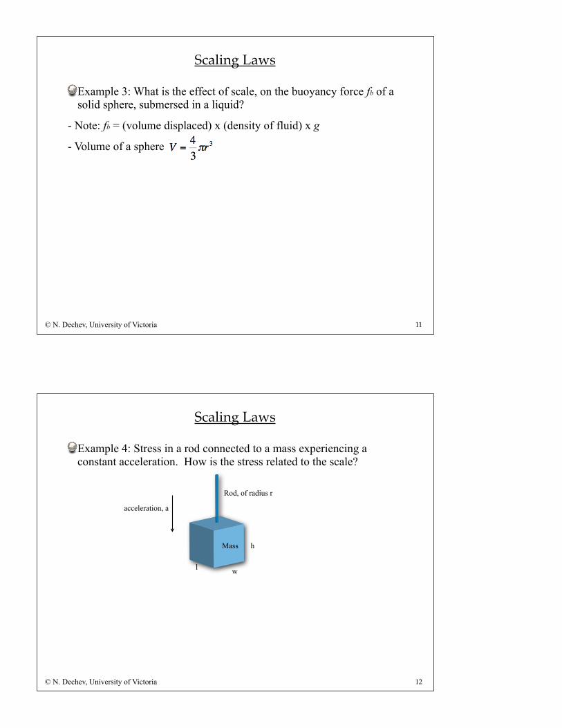
Example 4: Stress in a rod connected to a mass experiencing a constant acceleration. How is the stress related to the scale?
Scaling Laws
Mass
l
Rod, of radius r
w
h
acceleration, a
© N. Dechev, University of Victoria
13
Scaling Laws
Mass
l
r
w
h
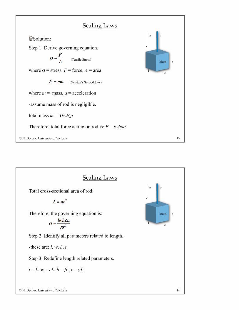
aSolution:
Step 1: Derive governing equation.
(Tensile Stress)
where σ = stress, F = force, A = area
(Newton’s Second Law)
where m = mass, a = acceleration
-assume mass of rod is negligible.
total mass m = (lwh)ρ
Therefore, total force acting on rod is: F = lwhρa
© N. Dechev, University of Victoria
14
Scaling Laws
Total cross-sectional area of rod:
Therefore, the governing equation is:
Step 2: Identify all parameters related to length.
-these are: l, w, h, r
Step 3: Redefine length related parameters.
l = L, w = eL, h = fL, r = gL
Mass
l
r
w
h
a
© N. Dechev, University of Victoria

15
Scaling Laws
Step 4: Re-write Expression.
Therefore, σ ∝ L.
- as L increases, σ increases proportionally.- as L decreases, σ decreases proportionally.
Question: If the dimensions of this system were all increased by a factor of 10x, (l, w, h, and r), is there a greater risk of rod failure?
Answer: Yes. Internal rod stress is 10x greater than before.
Mass
l
r
w
h
a
© N. Dechev, University of Victoria
16
Microfabrication
MEMS are fabricated with a set of technologies closely related to IC (integrated circuit) fabrication.
Silicon is the base substrate for many microelectronic technologies due to its semiconducting properties.
A semiconductor is a class of material where the conductivity of the material can be controlled by various means such as doping, temperature, light, electric fields, and other means.
Microelectronic microfabrication has been extensively developed over the past 40 years, and the technology and infrastructure is well established to work with silicon.
© N. Dechev, University of Victoria
17
MicrofabricationFrom Sand to Chips
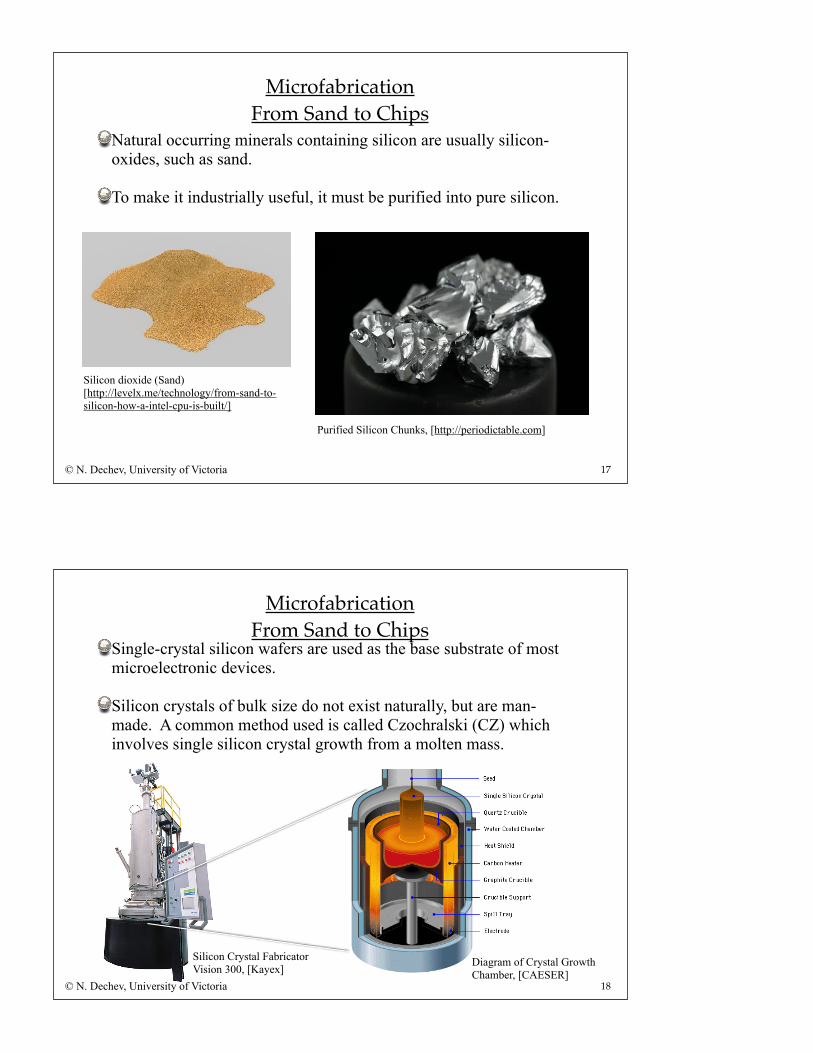
Natural occurring minerals containing silicon are usually silicon-oxides, such as sand.
To make it industrially useful, it must be purified into pure silicon.
© N. Dechev, University of Victoria
Purified Silicon Chunks, [http://periodictable.com]
Silicon dioxide (Sand)[http://levelx.me/technology/from-sand-to-silicon-how-a-intel-cpu-is-built/]
18
MicrofabricationFrom Sand to Chips
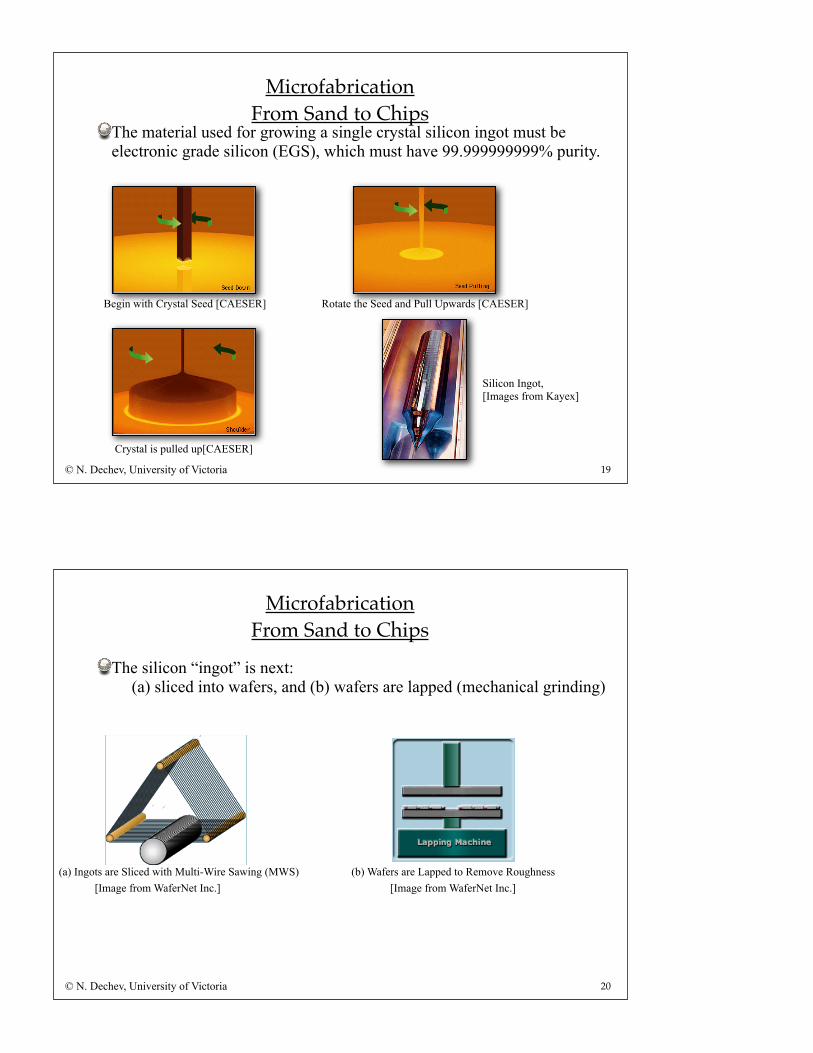
Single-crystal silicon wafers are used as the base substrate of most microelectronic devices.
Silicon crystals of bulk size do not exist naturally, but are man-made. A common method used is called Czochralski (CZ) which involves single silicon crystal growth from a molten mass.
Silicon Crystal FabricatorVision 300, [Kayex] Diagram of Crystal Growth
Chamber, [CAESER]© N. Dechev, University of Victoria
19
MicrofabricationFrom Sand to Chips
The material used for growing a single crystal silicon ingot must be electronic grade silicon (EGS), which must have 99.999999999% purity.
Crystal is pulled up[CAESER]
Silicon Ingot,[Images from Kayex]
Begin with Crystal Seed [CAESER] Rotate the Seed and Pull Upwards [CAESER]
© N. Dechev, University of Victoria
20
MicrofabricationFrom Sand to Chips
The silicon “ingot” is next: (a) sliced into wafers, and (b) wafers are lapped (mechanical grinding)
[Image from WaferNet Inc.](a) Ingots are Sliced with Multi-Wire Sawing (MWS) (b) Wafers are Lapped to Remove Roughness
© N. Dechev, University of Victoria
[Image from WaferNet Inc.]
21
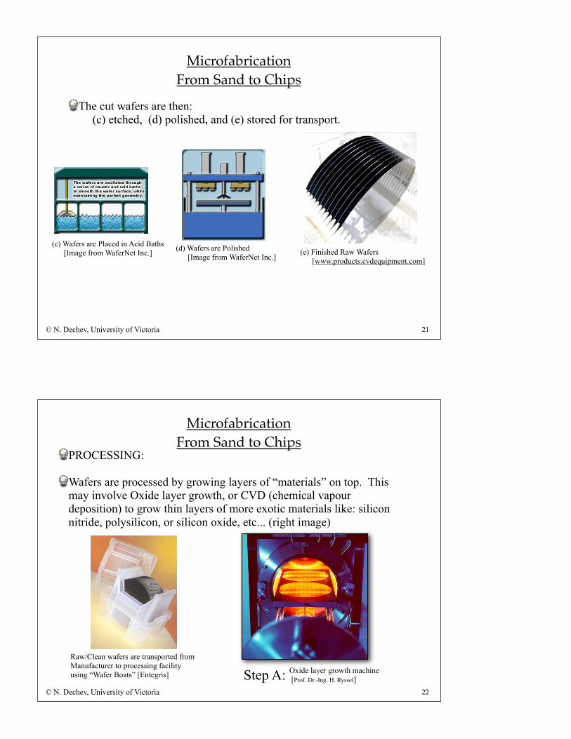
MicrofabricationFrom Sand to Chips
The cut wafers are then:(c) etched, (d) polished, and (e) stored for transport.
(d) Wafers are Polished [Image from WaferNet Inc.]
(c) Wafers are Placed in Acid Baths [Image from WaferNet Inc.]
© N. Dechev, University of Victoria
(e) Finished Raw Wafers [www.products.cvdequipment.com]
22
MicrofabricationFrom Sand to Chips
Raw/Clean wafers are transported from Manufacturer to processing facilityusing “Wafer Boats” [Entegris]
© N. Dechev, University of Victoria
Oxide layer growth machine [Prof. Dr.-Ing. H. Ryssel]
PROCESSING:
Wafers are processed by growing layers of “materials” on top. This may involve Oxide layer growth, or CVD (chemical vapour deposition) to grow thin layers of more exotic materials like: silicon nitride, polysilicon, or silicon oxide, etc... (right image)
Step A:

23
MicrofabricationFrom Sand to Chips
Spin Coating Process[www.phonon.com]
© N. Dechev, University of Victoria
PROCESSING:
“Spin Coating” is used to deposit thin layers of polymers onto wafers.
Hot Plate for thermal cure OR thermal drying of polymers on wafers
Step B: Step B1:
24
MicrofabricationFrom Sand to Chips
Chrome Mask[http://semimd.com]
© N. Dechev, University of Victoria
PROCESSING:
“Chrome Masks” with UV exposure are used to selectively “cure” the polymer and change its properties in specific areas.
Mask Aligner and UV Exposure system[http://cnst.nist.gov/nanofab]
Step C:

25
MicrofabricationFrom Sand to Chips
© N. Dechev, University of Victoria
PROCESSING:
The regions/areas of the polymer that were not exposed to UV light must be ‘etched/removed’ with a solvent wash.
Solvent Rinse to “Etch” away polymer that was exposed to UV light (previous step)[www.daitron.com]
Step D:Step F:
26
MicrofabricationFrom Sand to Chips
© N. Dechev, University of Victoria
PROCESSING:
The regions/areas of the polymer that were not exposed to UV light must be ‘etched/removed’ with a solvent wash.
Reactive Ion Etching (Diagram)[Michael Huff, J. of Sensor Review] Reactive Ion Etching Machine
[http://en.wikipedia.org/wiki/Reactive-ion_etching]Step E:

27
MicrofabricationFrom Sand to Chips
Complete processed wafer withCMOS, etc... [Siemens]
© N. Dechev, University of Victoria
Surface micromachining Steps A to F are repeated for “each layer” on a chip.
Multiple layers are created for the electrical or mechanical layers that make the circuit, transistors, resistors, structure, etc... For example, the CMOS wafer with dozens of chip patterns, shown on the left.
The MEMS-based MUMPs process (described on pp. 33-38) uses 100 mm wafers, with 10x10 mm chip patterns.
A typical ‘chip pattern’ may be up to 10 mm x 10 mm in size. Hence the pattern is duplicated many times onto a round silicon wafer, to best utilize the area.
28
MicrofabricationFrom Sand to Chips
© N. Dechev, University of Victoria
Individual chips (regions) on wafers are inspected and tested.[Dr. Rer.Nat. L. Frey]
For microelectronics, the ‘chip patterns’ must first be inspected before the wafer is diced (cut up into rectangular pieces).
A multi-tip probe (consisting of 30+ tips) with an automatic machine is used to do this inspection procedure. The probes are pressed onto each chip pattern and electrical tests are performed to determine: function within allowed operating tolerances, maximum speed, etc...
Even on a single wafer, it is possible for different chip patterns to exhibit different electrical characteristics. This is micro-fabrication variability results in ‘grading chips’ to different quality.

29
MicrofabricationFrom Sand to Chips
Wafer is sliced into individual chip die [Majelac Technologies]
Loose die [N. Dechev]© N. Dechev, University of Victoria
The wafer is diced using diamond tipped circular saw.
The diced chips are sorted based on their previous inspection results.
They are now referred to as ‘loose die’ but due to their ‘micro-sized patterns’ they cannot connect to the outside world.
For most chips, the option exists to receive the loose die directly. For our laboratory, we will use our own probe tip to electrically interface with the chips.
30
MicrofabricationFrom Sand to Chips
Die are packaged into chip carriers or otherpackaging systems [Corwil Tech. Corp.]
Die pads are wire bonded to chip carrier leads [image from S. He]
© N. Dechev, University of Victoria
The loose die are packaged in some way to protect them from the environment. Microelectronic packaging is a large industry in and of itself!
Various chip carriers (enclosures) are available, from cheap black epoxy, to metal cans, to high quality ceramic+gold packages (shown below).
All microelectronic chips will have ‘bonding pads’ along their edge, to which tiny gold wires (25-50 um) are connected. The other end of these wires are connected to the leads on the chip carrier.

31
MicrofabricationFrom Sand to Chips
© N. Dechev, University of Victoria
Epoxy packaged 16-pin DIP (dual in-line pin) chip
The result is the ‘chip’ shown in its various forms below:
Ceramic packaged DIP chip
Epoxy packaged 44-pin surface mount chip [curiousinventor.com]
BGA (ball grid array) chip packaging systems [Digi-Key, Texas Instruments]
32
MEMS Microfabrication
There are two main microfabrication methods for MEMS:
•Bulk Micromachining, which is based on the etching and bonding of thick sheets of material such as silicon oxides and crystalline silicon.
•Wet Etching (Anisotropic, or Isotropic)
•Dry Etching (Plasma Etching, Reactive Ion Etching)
•Surface Micromachining, which is based on the successive deposition and etching of thin films of material such as silicon nitride, polysilicon, silicon oxide and gold.
•Multi-User MEMS Processes (MUMPs)
•Surface Micromachining with Planarization,(MEMX, formerly SUMMiT)
© N. Dechev, University of Victoria
33
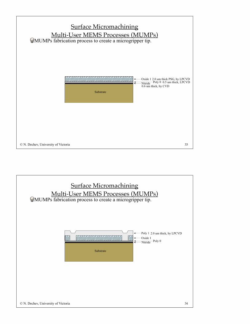
Surface MicromachiningMulti-User MEMS Processes (MUMPs)
MUMPs fabrication process to create a microgripper tip.
Substrate
Nitride0.6 um thick, by CVD
Poly 0 0.5 um thick, LPCVD Oxide 1 2.0 um thick PSG, by LPCVD
© N. Dechev, University of Victoria
34
Surface MicromachiningMulti-User MEMS Processes (MUMPs)
MUMPs fabrication process to create a microgripper tip.
Substrate
Nitride Poly 0Oxide 1
Poly 1 2.0 um thick, by LPCVD
© N. Dechev, University of Victoria

35
Surface MicromachiningMulti-User MEMS Processes (MUMPs)
MUMPs fabrication process to create a microgripper tip.
Substrate
Nitride Poly 0Oxide 1
Poly 1Oxide 2 0.75 um thick PSG, by LPCVD Poly 2 1.5 um thick, by LPCVD
© N. Dechev, University of Victoria
36
Surface MicromachiningMulti-User MEMS Processes (MUMPs)
MUMPs fabrication process to create a microgripper tip.
Substrate
Nitride Poly 0Oxide 1
Poly 1Oxide 2
Poly 2Metal
0.5 um thick Gold, by ‘lift-off patterning’ (requires no etch)
© N. Dechev, University of Victoria

37
Surface MicromachiningMulti-User MEMS Processes (MUMPs)
MUMPs fabrication process to create a microgripper tip.
Oxide Release process to ‘free microstructures’ from substrate.
Etch away Oxide 1 and Oxide 2 with HF.
Substrate
Nitride Poly 0
Poly 1
Oxide 1
Oxide 2
Poly 2Metal
© N. Dechev, University of Victoria
38
Surface MicromachiningMulti-User MEMS Processes (MUMPs)
MUMPs fabrication process to create a microgripper tip.
Oxide Release process to ‘free microstructures’ from substrate.
Released Structure!
Substrate
Nitride Poly 0
Poly 1
Poly 2Metal
© N. Dechev, University of Victoria

39
Surface MicromachiningMulti-User MEMS Processes (MUMPs)
MUMPs fabrication process to create a microgripper tip.
Section A Poly 2 Gripper Tip
Poly 1 LiftStructure
Poly 1Poly 2
Substrate
Substrate
2 μm
2.75 μm
Poly 1
Poly 2
Oxide 1
Poly 2
Gripper Tip
Gripper Tip
Upper Level
Poly 1 Lift Structure
Anchor 1
Oxide 2
Microgripper tip fabricated with MUMPs[N. Dechev]
© N. Dechev, University of Victoria