lecture 10: efficient design of current-starved vco · advanced topics in vlsi systems instructor:...
TRANSCRIPT
CSCE 6933/5933 Advanced Topics in VLSI Systems
Instructor: Saraju P. Mohanty, Ph. D.
1
Lecture 10: Efficient Design
of Current-Starved VCO
NOTE: The figures, text etc included in slides are borrowed from various books, websites, authors pages, and other sources for academic purpose only. The instructor does not claim any originality.
Advanced Topics in VLSI Systems

Unified P4 (Power-Performance-
Process-Parasitic) Fast Optimization of a
Nano-CMOS VCO
Advanced Topics in VLSI Systems 2
Outline of the Talk
• Introduction • Novel Contributions • Related Prior Research • Proposed Novel RFIC P4 Optimal Design Flow • Design of 90nm CMOS VCO • Process Variation Analysis of VCO • P4 Optimization of VCO • Conclusions and Future Research
3 Advanced Topics in VLSI Systems

Introduction • Radio Frequency Integrated Circuits (RFICs) are becoming
performance-oriented. The battle to deliver maximum performance has taken center stage. (Performance)
• Power-aware design is required to maximize some performance metric, subject to a power budget. (Power)
• Also, potential yield loss is caused by increasing process variations. Impact of process variations on the performance factors of a design is much higher for today’s nanometer. (Process)
• In high frequency application circuits, the exact performance prediction is challenging due to many parasitic effects. It is crucial to be able to predict parasitic effects for accurate performance. (Parasitic)
Advanced Topics in VLSI Systems
4

Novel Contributions • A P4 (Power-Performance-Parasitic-Process) optimal
design flow for RF circuits is proposed. • Nano-CMOS current starved VCO subjected to design
flow. • P4 optimization of the VCO is carried out using a dual-
oxide process technique. • A dual-oxide physical design of the VCO is presented for
90nm CMOS technology. • A novel process variation analysis technique called
Design of Experiments-Monte Carlo (DOE-MC) approach is proposed, offering up to 6.25X computational time savings over traditional Monte-Carlo (TMC).
Advanced Topics in VLSI Systems
5

Related Prior Research
Reference Technology Performance Power
Tiebout et. al. 250nm 1.8GHz 20mW
Dehghani et.al. 250nm 2.5GHz 2.6mW
Long et. al. 180nm 2.4GHz 1.8mW
Kwok et. al. 180nm 1.4GHz 1.46mW
This Design 90nm dual-
oxide
2.3GHz 158µW
Advanced Topics in VLSI Systems
6
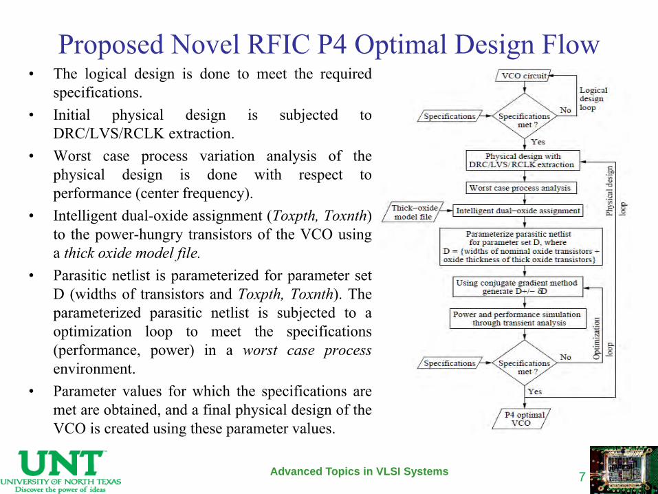
Proposed Novel RFIC P4 Optimal Design Flow • The logical design is done to meet the required
specifications. • Initial physical design is subjected to
DRC/LVS/RCLK extraction. • Worst case process variation analysis of the
physical design is done with respect to performance (center frequency).
• Intelligent dual-oxide assignment (Toxpth, Toxnth) to the power-hungry transistors of the VCO using a thick oxide model file.
• Parasitic netlist is parameterized for parameter set D (widths of transistors and Toxpth, Toxnth). The parameterized parasitic netlist is subjected to a optimization loop to meet the specifications (performance, power) in a worst case process environment.
• Parameter values for which the specifications are met are obtained, and a final physical design of the VCO is created using these parameter values.
Advanced Topics in VLSI Systems
7
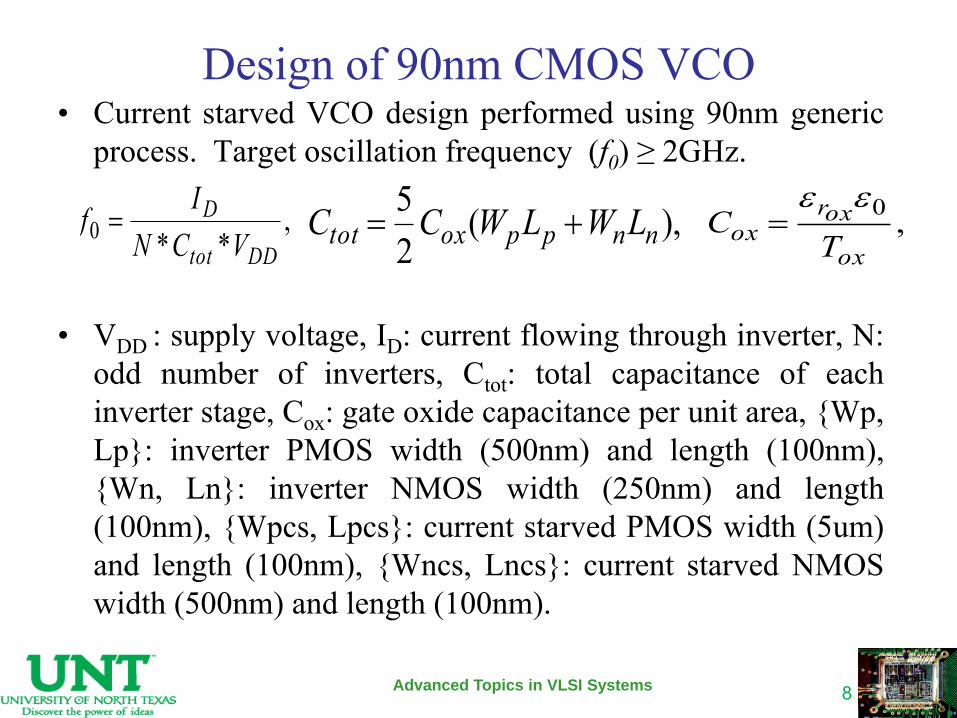
Design of 90nm CMOS VCO • Current starved VCO design performed using 90nm generic
process. Target oscillation frequency (f0) ≥ 2GHz.
• VDD : supply voltage, ID: current flowing through inverter, N:
odd number of inverters, Ctot: total capacitance of each inverter stage, Cox: gate oxide capacitance per unit area, {Wp, Lp}: inverter PMOS width (500nm) and length (100nm), {Wn, Ln}: inverter NMOS width (250nm) and length (100nm), {Wpcs, Lpcs}: current starved PMOS width (5um) and length (100nm), {Wncs, Lncs}: current starved NMOS width (500nm) and length (100nm).
,**0
DDtot
DVCN
If ),(25
nnppoxtot LWLWCC ,0
ox
oxrox T
C
Advanced Topics in VLSI Systems
8

Design of 90nm CMOS VCO
Advanced Topics in VLSI Systems
9

Process Variation Analysis of VCO: TMC • Process variation analysis has been carried
out on the initial physical design with parasitics extracted (RLCK).
• Variation in 5 parameters: – VDD: Supply voltage, – Vtn: NMOS threshold voltage, – Vtp: PMOS threshold voltage, – Toxn: NMOS gate oxide thickness, – Toxp: PMOS gate oxide thickness.
• Process parameters assumed to have a Gaussian distribution with mean (μ) as the nominal value in the process design kit, and a standard deviation (σ) as 10% of the mean. TMC with 1000 runs gives the oscillation frequency (f0) having a Gaussian distribution with μ = 1.54 GHz, σ = 103.5 MHz.
Advanced Topics in VLSI Systems
10

Process Variation Analysis of VCO: DOE-MC • The DOE-MC methodology offers the
advantage of faster computation over TMC.
• A two level full factorial design is run for the 5 process parameters, where:
– Level 1: μ - 2 × σ, – Level 2: μ + 2 × σ.
• A full factorial run requires 25 = 32 trials. 5 MC replicate runs are run for every trial. μ(f0) and σ(f0) are recorded. We obtain 32 values of μ(f0) and σ(f0).
• The final μ(f0) and σ(f0) are recorded as the average of the 32 trials. Considering 5 replicates per trial, we get a total of 32 × 5 = 160 runs (compared to 1000 TMC runs).
Advanced Topics in VLSI Systems
11
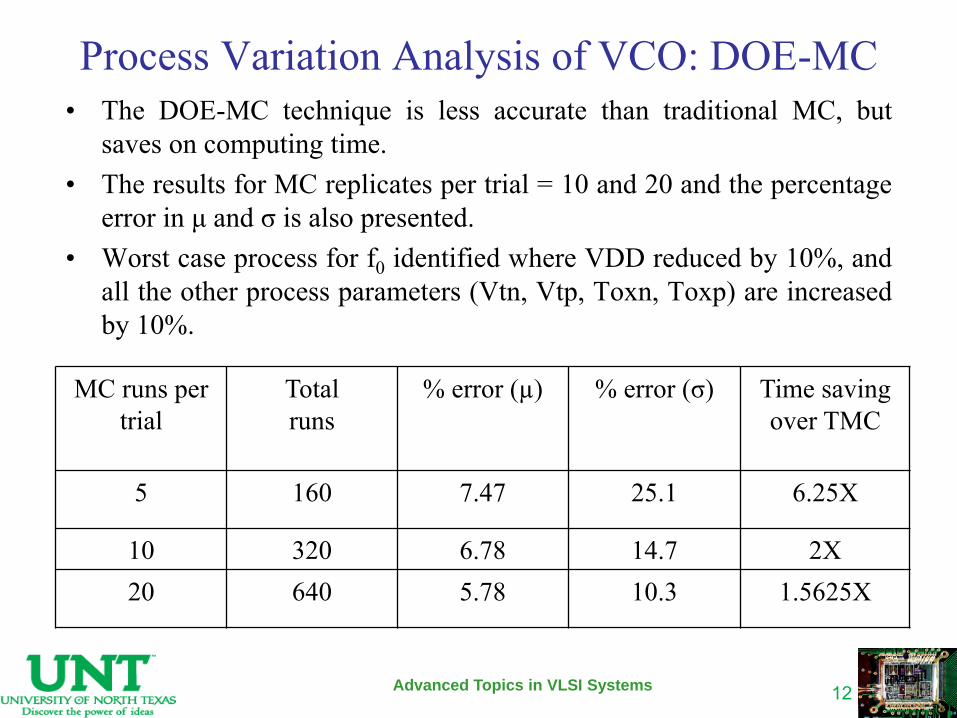
Process Variation Analysis of VCO: DOE-MC • The DOE-MC technique is less accurate than traditional MC, but
saves on computing time. • The results for MC replicates per trial = 10 and 20 and the percentage
error in μ and σ is also presented. • Worst case process for f0 identified where VDD reduced by 10%, and
all the other process parameters (Vtn, Vtp, Toxn, Toxp) are increased by 10%.
MC runs per trial
Total runs
% error (µ) % error (σ)
Time saving over TMC
5 160 7.47 25.1 6.25X
10 320 6.78 14.7 2X 20 640 5.78 10.3 1.5625X
Advanced Topics in VLSI Systems
12

P4 Optimization of VCO • Logical design center
frequency f0 = 2 GHz. • Initial physical design
center frequency f0p = 1.56 GHz (25% degradation).
• Initial physical design center frequency in a worst case process variation environment f0p−p = 1.13 GHz (43.5% degradation).
• Initial average power consumption (including leakage) (PVCO) = 212μW.
Advanced Topics in VLSI Systems
13
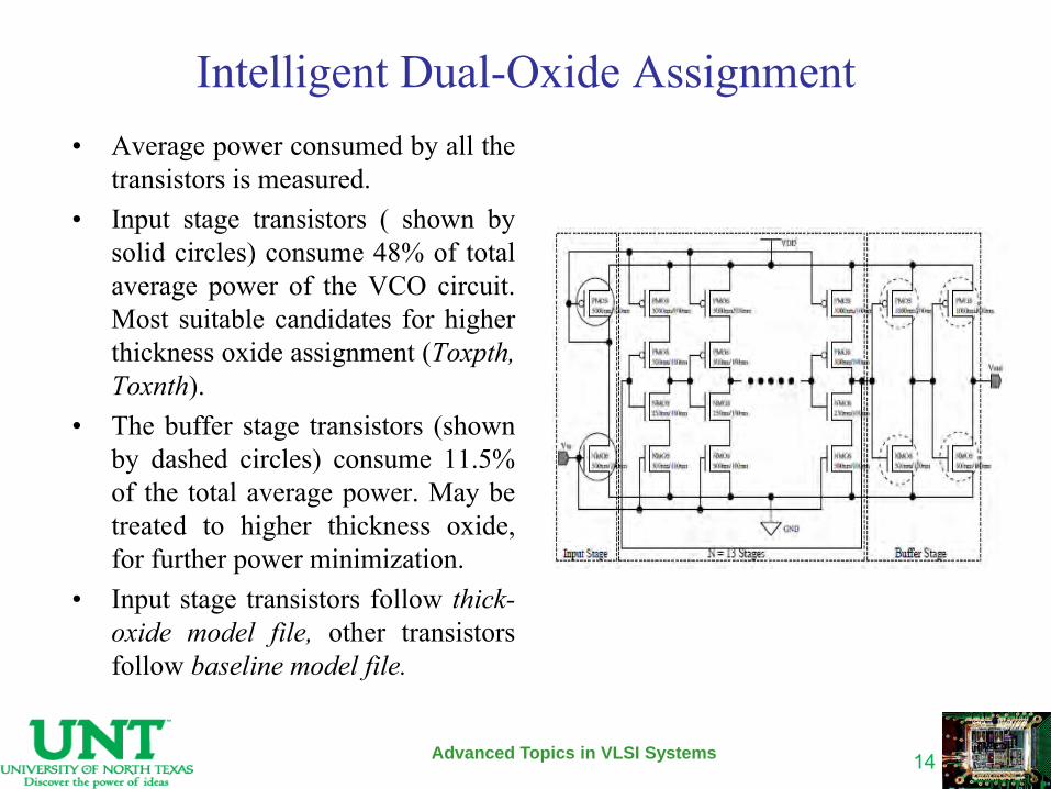
Intelligent Dual-Oxide Assignment • Average power consumed by all the
transistors is measured. • Input stage transistors ( shown by
solid circles) consume 48% of total average power of the VCO circuit. Most suitable candidates for higher thickness oxide assignment (Toxpth, Toxnth).
• The buffer stage transistors (shown by dashed circles) consume 11.5% of the total average power. May be treated to higher thickness oxide, for further power minimization.
• Input stage transistors follow thick-oxide model file, other transistors follow baseline model file.
Advanced Topics in VLSI Systems
14

Conjugate Gradient Optimization • Input: Parasitic parameterized netlist, Baseline model file, Thick oxide model file,
Objective set F = [ f0, PVCO ], Stopping criteria S, design variable set D = [ Wn, Wp, Wncs, Wpcs, Toxpth, Toxnth ], Lower design constraint Clow, Upper design constraint Cup.
• Output: Optimized objective set Fopt, Optimal design variable set Dopt for S = ± β, {where 1% ≤ β ≤ 5%}.
• Run initial simulation in order to obtain feasible values of design variables for the given specifications.
• while (Clow < D < Cup) do
• Using conjugate gradient, generate new set of design variables D’ = D ± δD. • Compute objective set F = [ f0, PVCO ]. • if (S == ± β) then
• return Dopt = D’. • end if
• end while
• Using Dopt, construct final physical design and simulate. • Record Fopt.
Advanced Topics in VLSI Systems
15

Conjugate Gradient Optimization • Target center frequency f0 = 2GHz. • Final Physical design center frequency f0p = 2.3GHz. • Final Physical design center frequency in a worst case process variation
environment f0p−p = 1.98GHz (1% discrepancy). • Final average power consumption (including leakage) (PVCO) = 158μW
(25% reduction). D Clow Cup Dopt
Wn 200nm 500nm 210nm
Wp 400nm 1µm 415nm
Wncs 1µm 10µm 8.5µm
Wpcs 5µm 10µm 5µm
Toxpth 2.48nm 5nm 5nm
Toxnth 2.33nm 5nm 3.54nm
Advanced Topics in VLSI Systems
16
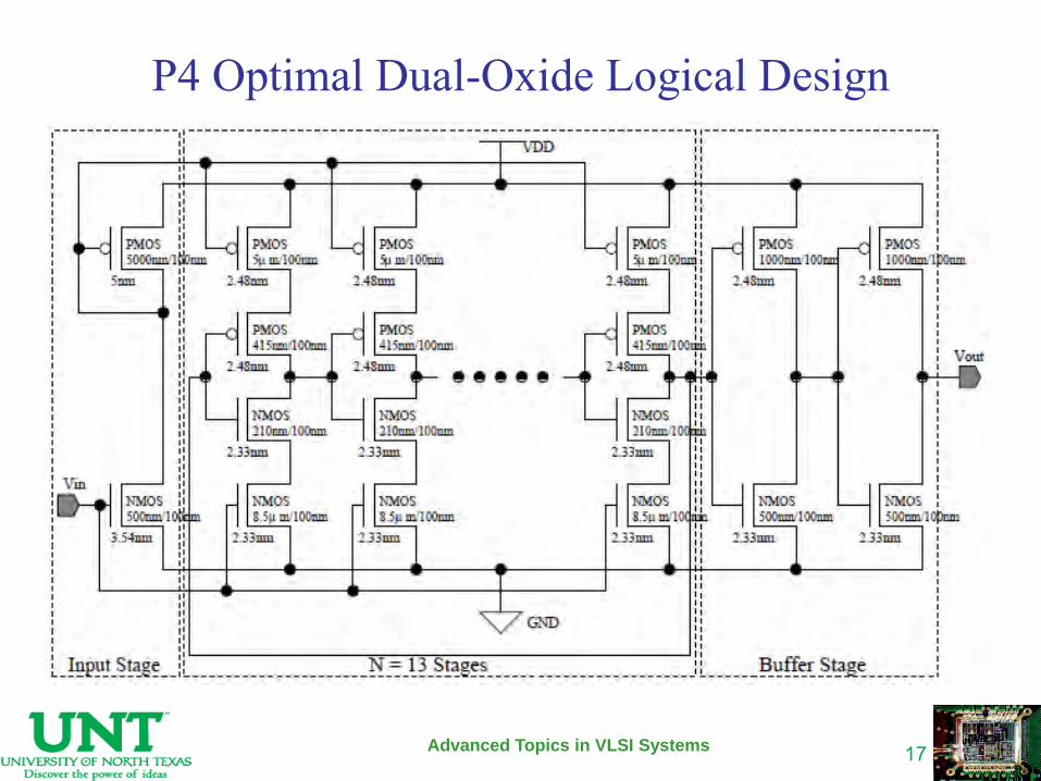
P4 Optimal Dual-Oxide Logical Design
Advanced Topics in VLSI Systems
17

P4 Optimal Dual-Oxide Physical Design
2/2/2012 Advanced Topics in VLSI Systems
18

Conclusions and Future Research • Design of a P4 (Power-Performance-Parasitic-Process) optimal
nano-CMOS VCO is proposed. The presented design flow may be used for optimization of nanoscale circuits in general.
• The center frequency treated as the target specification. The degradation of the center frequency due to parasitic and process variation effects narrowed down from 43.5% to 1%, along with 25% power minimization using dual-oxide technique.
• The end product of the proposed design flow is a P4 optimal dual-oxide VCO physical design.
• For future research, we plan to consider thermal effects in the VCO design as well.
• Alternative optimization techniques such as simulated annealing and genetic algorithms are also being explored for a fair comparison of the P4 design flow with other approaches.
Advanced Topics in VLSI Systems
19

A P4VT (Power-Performance-Process-
Parasitic-Voltage-Temperature) Aware
Dual-VTh Nano-CMOS VCO
Advanced Topics in VLSI Systems
20
Outline of the Talk
• Introduction • Novel Contributions of this paper • Related Prior Research • Proposed Novel P4VT Aware Design Flow • Logical Design of VCO • PVT Variation Analysis of VCO • P4VT Optimization of VCO • Conclusions and Future Research
Advanced Topics in VLSI Systems
21

Introduction …
• Power-Performance: Radio Frequency Integrated Circuits (RFICs) must be simultaneously:
• Low power consuming • High performance
• Process-Voltage: Impact of process and supply voltage variations on the performance factors of a design is much higher for nanometer technologies.
Advanced Topics in VLSI Systems
22

Introduction
• Parasitics: In high frequency application circuits, the exact performance prediction is challenging due to many parasitic effects. It is crucial to be able to account parasitic effects for accurate performance.
• Temperature: There is a need for temperature-aware design methodologies in order to produce properly functioning and reliable silicon.
Advanced Topics in VLSI Systems
23

Novel Contributions of This Paper • A Power-Performance-Parasitic-Process-Voltage-
Temperature (called P4VT) aware optimization flow for nanoscale CMOS analog circuits is introduced.
• The design of a P4VT-aware RF nano-CMOS circuit, VCO is discussed.
• For power optimization of the VCO, a dual-threshold process level technique is discussed.
• A dual-threshold physical design of the optimized VCO is presented.
Advanced Topics in VLSI Systems
24
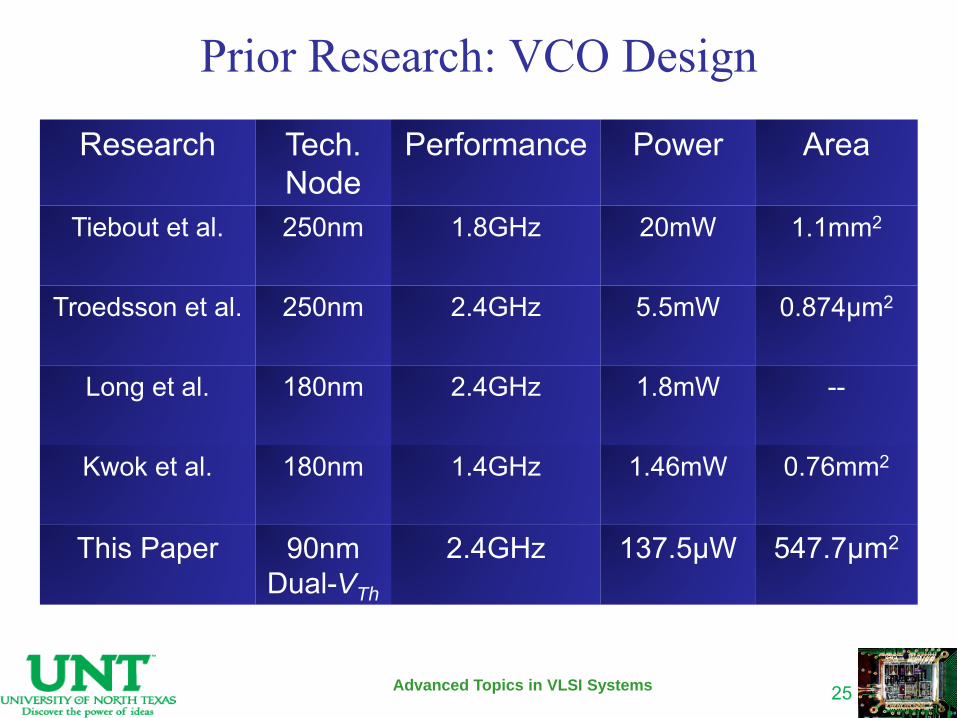
Prior Research: VCO Design
Research Tech. Node
Performance Power Area
Tiebout et al. 250nm 1.8GHz 20mW 1.1mm2
Troedsson et al. 250nm 2.4GHz 5.5mW 0.874µm2
Long et al. 180nm 2.4GHz 1.8mW --
Kwok et al. 180nm 1.4GHz 1.46mW 0.76mm2
This Paper 90nm Dual-VTh
2.4GHz 137.5µW 547.7µm2
Advanced Topics in VLSI Systems
25

Prior Research: PVT Tolerance • Kim 2009: PVT-tolerance using supply/body-
bias voltage generation. • Charan 2008: Corner analysis used for PVT-
tolerant humidity sensor. • Miyashita 2005: Automatic amplitude control is
used to reduce PVT variation in LC-VCO. • Kondou 2007: Two on-chip digital calibration
circuits are used for PVT-tolerant PLL.
Advanced Topics in VLSI Systems
26
Prior Research: Parasitic Tolerance • Park 2003: Parasitic-Aware optimization of
CMOS wideband amplifier. • Choi 2006: Simulated annealing optimization for
parasitic-aware RF power amplifier. • Choi 2003: Particle swarm optimization
techniques for parasitic-aware CMOS RF circuits.
Advanced Topics in VLSI Systems
27

Proposed Novel P4VT Aware Design Flow … • Logical design performed to
meet the specifications. • Preliminary physical layout
subjected to DRC/LVS/RCLK. • RCLK extracted physical design
is subjected to process, voltage and temperature variation analysis.
• Dual-threshold assignment (HVThn , HVThp) to the power-hungry transistors of the VCO.
Advanced Topics in VLSI Systems
28

Proposed Novel P4VT Aware Design Flow • Parasitic netlist is parameterized
for parameter set D (widths of transistors and HVThn , HVThp).
• Parameterized netlist is subjected to optimization for worst case PVT variations.
• Parameter values for which the specifications are met are determined.
• Final physical design of the VCO is performed using these parameter values.
Advanced Topics in VLSI Systems
29

Center Frequency (f0) vs. Temperature
Non-Optimized VCO P4VT Optimized VCO
Advanced Topics in VLSI Systems
30

Logical Design of 90nm CMOS VCO • Current starved VCO design performed using 90nm
process. Following equations are used:
DDtot
D
VCNIf
**0
)(25
nnppoxtot LWLWCC
ox
rox T
C ox 0
VDD : supply voltage, ID: current flowing through inverter, N: odd number of inverters, Ctot: total capacitance of each inverter stage, Cox: gate oxide capacitance per unit area.
Advanced Topics in VLSI Systems
31

Logical Design of 90nm CMOS VCO
• For a target oscillation frequency (f0) ≥ 2GHz for 90nm node:
{Wp, Lp}: inverter PMOS width (500nm) and length (100nm). {Wn, Ln}: inverter NMOS width (250nm) and length (100nm) {Wpcs, Lpcs}: current starved PMOS width (5um) and length
(100nm) {Wncs, Lncs}: current starved NMOS width (500nm) and
length (100nm).
Advanced Topics in VLSI Systems
32

Logical Design of 90nm CMOS VCO
Advanced Topics in VLSI Systems
33

PVT Variation Analysis of VCO • Process-voltage variation analysis has
been carried out on the initial physical design with parasitics (RLCK) extracted netlist.
• Monte Carlo simulation for 1000 runs performed for variation in 5 parameters: – VDD: Supply voltage – VThn: NMOS threshold voltage – VThp: PMOS threshold voltage – Toxn: NMOS gate oxide thickness – Toxp: PMOS gate oxide thickness.
• for temperatures = 27°C, 50°C, 75°C, 100°C, 125°C.
for 27°C
Advanced Topics in VLSI Systems
34

PVT Variation Analysis of VCO
• The worst-case process variation is where VThn, VThp, Toxn, Toxp) are increased by 10%.
• The worst-case voltage variation is where VDD is reduced by 10%.
• The worst-case temperature variation is 125°C.
Advanced Topics in VLSI Systems
35

P4VT Optimization of VCO • Logical design center
frequency f0 ≥ 2 GHz. • Preliminary physical design
center frequency f0p = 1.56 GHz (25% degradation).
• Preliminary physical design center frequency in worst case PVT conditions f0pvt = 1 GHz (50% degradation).
• Initial average power consumption (including leakage) (PVCO) = 164.5μW.
Advanced Topics in VLSI Systems
36

Dual-Threshold Assignment in VCO …
• Average power consumed by all the transistors is measured.
• Input stage transistors (shown by solid circles) consume 48% of total average power of the VCO circuit.
• Most suitable candidates for higher threshold voltage assignment (HVThn , HVThp).
Advanced Topics in VLSI Systems
37

Dual-Threshold Assignment in VCO
• The buffer stage transistors (shown by dashed circles) consume 11.5% of the total average power.
• May be treated to higher threshold voltage, for further power minimization.
• Input stage transistors follow high threshold model file, other transistors follow baseline model file.
Advanced Topics in VLSI Systems
38

Power-Performance Optimization in VCO …
• The parasitic aware netlist generated from the preliminary layout is parameterized with respect to the optimization parameter set D, which includes: – Widths of PMOS and NMOS devices in the
inverter (Wn,Wp), – Widths of PMOS and NMOS devices in the
current-starved circuitry (Wncs,Wpcs), – HVThn, HVThp.
Advanced Topics in VLSI Systems
39

Power-Performance Optimization
• The parameterized netlist is subjected to power-performance optimization using a conjugate gradient method.
• Our objective set are f0 ≥ 2GHz, and PVCO = minimum.
• S is the stopping criteria for the optimization to stop when the objective set is within ±ε.
• ε is a designer specified error percentage.
Advanced Topics in VLSI Systems
40

One Optimization Algorithm • Input: Parasitic aware netlist, Baseline model file, High threshold model file, Objective
set F = [ f0, PVCO ], Stopping criteria S, parameter set D = [ Wn, Wp, Wncs, Wpcs, HVThn , HVThp ], Lower design constraint Clow, Upper design constraint Cup.
• Output: Optimized objective set Fopt , Optimal parameter set Dopt for S ≤ ±ε, {where ε=10%}.
• Perform first iteration with initial guess of D. • while (Clow < D < Cup) do
• Using conjugate gradient, generate D’ = D ± ΔD in the direction of travel of Fopt ±ε. • Compute objective set F( D’ ) = [ f0, PVCO ]. • Compute S as the difference of target objective set and current objective set. • if S ≤ ε then
{stopping criteria is within the error margin} • return Dopt = D’. • end if
• end while
• Using Dopt, construct final physical design and simulate. • Record Fopt accounting the full-blown parasitics.
Advanced Topics in VLSI Systems
41

Optimization Results • Target center frequency f0 ≥ 2GHz. • Final Physical design center frequency f0p = 2.4GHz. • Final Physical design center frequency in a worst case PVT
conditions f0pvt = 1.8GHz (10% discrepancy). • Final average power consumption (including leakage) (PVCO) =
137.5μW (16.4% reduction). D Clow Cup Dopt
Wn 200nm 500nm 390nm
Wp 400nm 1µm 445nm
Wncs 1µm 50µm 10µm
Wpcs 5µm 50µm 30µm
Toxpth 0.1692662V 0.5V 0.5V
Toxnth -0.5V -0.1359511V -0.4975V
Advanced Topics in VLSI Systems
42
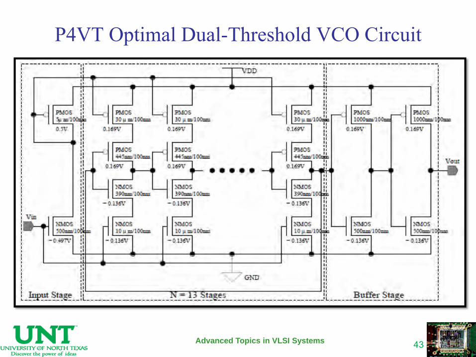
P4VT Optimal Dual-Threshold VCO Circuit
Advanced Topics in VLSI Systems
43

P4VT Optimal Dual-Threshold VCO Layout
Advanced Topics in VLSI Systems
44

P4VT-Aware Performance of VCO
Advanced Topics in VLSI Systems
45

Summary and Conclusions …
• Design of a Power-Performance-Parasitic-Process-Voltage-Temperature (P4VT) optimal nano-CMOS VCO is proposed.
• The presented design flow is used on top of existing physical design tools.
• The center frequency treated as the target specification. • The degradation of the center frequency due to worst-
case PVT effects narrowed down from 50% to 10%.
Advanced Topics in VLSI Systems
46

Summary and Conclusions
• 16.4% power minimization is achieved using dual-threshold technique.
• The end product of the proposed design flow is a P4VT optimal dual-threshold VCO physical design that meets the functional specifications across entire temperature range.
• For future research, we plan to incorporate additional performance criteria to the optimization set, such as phase noise.
Advanced Topics in VLSI Systems
47