lbi-38864b - monogram series vhf mobile radio model … · monogram series vhf mobile radio ... doc...
TRANSCRIPT
ericssonz
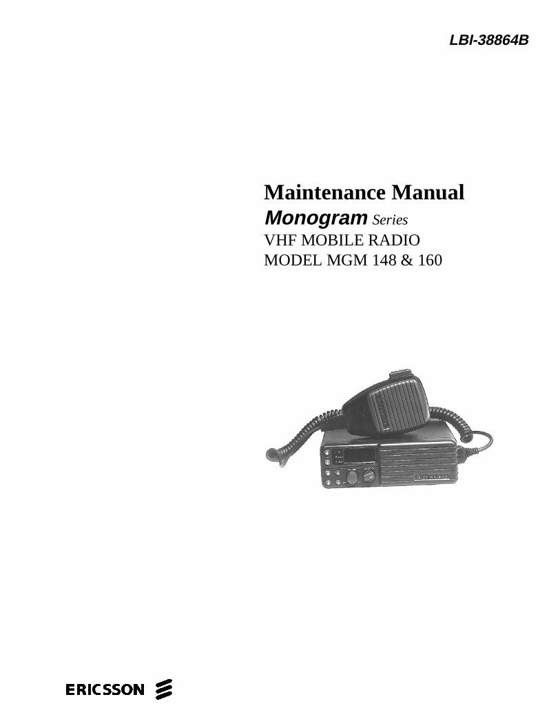
LBI-38864B
Maintenance ManualMonogram Series
VHF MOBILE RADIOMODEL MGM 148 & 160
TABLE OF CONTENTS
SPECIFICATIONS . . . . . . . . . . . . . . . . . . . . . . . . . . . . . . . . . . . . . . . . . . . . . . . . . . . . . . . . . . . . . . . . . . . . . . . . . 1-4
Receiver (PER EIA RS-204-C) . . . . . . . . . . . . . . . . . . . . . . . . . . . . . . . . . . . . . . . . . . . . . . . . . . . . . . . . . . . 2
Transmitter (PER EIA RS-152-B). . . . . . . . . . . . . . . . . . . . . . . . . . . . . . . . . . . . . . . . . . . . . . . . . . . . . . . . . 3
Options And Accessories . . . . . . . . . . . . . . . . . . . . . . . . . . . . . . . . . . . . . . . . . . . . . . . . . . . . . . . . . . . . . . . 4
UNPACKING . . . . . . . . . . . . . . . . . . . . . . . . . . . . . . . . . . . . . . . . . . . . . . . . . . . . . . . . . . . . . . . . . . . . . . . . . . . . . . . 5
GENERAL DESCRIPTION . . . . . . . . . . . . . . . . . . . . . . . . . . . . . . . . . . . . . . . . . . . . . . . . . . . . . . . . . . . . . . . . . . . 6
DESCRIPTION OF CONTROLS. . . . . . . . . . . . . . . . . . . . . . . . . . . . . . . . . . . . . . . . . . . . . . . . . . . . . . . . . . . . . . . 7-8
Front Panel Controls . . . . . . . . . . . . . . . . . . . . . . . . . . . . . . . . . . . . . . . . . . . . . . . . . . . . . . . . . . . . . . . . . . 7
Rear Panel Controls . . . . . . . . . . . . . . . . . . . . . . . . . . . . . . . . . . . . . . . . . . . . . . . . . . . . . . . . . . . . . . . . . . . 8
GENERAL OPERATION . . . . . . . . . . . . . . . . . . . . . . . . . . . . . . . . . . . . . . . . . . . . . . . . . . . . . . . . . . . . . . . . . . . . . 9-10
Radio On/off, Power Up . . . . . . . . . . . . . . . . . . . . . . . . . . . . . . . . . . . . . . . . . . . . . . . . . . . . . . . . . . . . . . . . 9
Receiving. . . . . . . . . . . . . . . . . . . . . . . . . . . . . . . . . . . . . . . . . . . . . . . . . . . . . . . . . . . . . . . . . . . . . . . . . . . . 9
Transmitting . . . . . . . . . . . . . . . . . . . . . . . . . . . . . . . . . . . . . . . . . . . . . . . . . . . . . . . . . . . . . . . . . . . . . . . . . 9
Digital Channel Guard. . . . . . . . . . . . . . . . . . . . . . . . . . . . . . . . . . . . . . . . . . . . . . . . . . . . . . . . . . . . . . . . . 10
CIRCUIT ANALYSIS . . . . . . . . . . . . . . . . . . . . . . . . . . . . . . . . . . . . . . . . . . . . . . . . . . . . . . . . . . . . . . . . . . . . . . . . 11-13
Receiver. . . . . . . . . . . . . . . . . . . . . . . . . . . . . . . . . . . . . . . . . . . . . . . . . . . . . . . . . . . . . . . . . . . . . . . . . . . . . 11
Transmitter . . . . . . . . . . . . . . . . . . . . . . . . . . . . . . . . . . . . . . . . . . . . . . . . . . . . . . . . . . . . . . . . . . . . . . . . . . 12
Frequency Synthesizer . . . . . . . . . . . . . . . . . . . . . . . . . . . . . . . . . . . . . . . . . . . . . . . . . . . . . . . . . . . . . . . . . 12
PREVENTIVE MAINTENANCE. . . . . . . . . . . . . . . . . . . . . . . . . . . . . . . . . . . . . . . . . . . . . . . . . . . . . . . . . . . . . . . 14
Connections . . . . . . . . . . . . . . . . . . . . . . . . . . . . . . . . . . . . . . . . . . . . . . . . . . . . . . . . . . . . . . . . . . . . . . . . . 14
Electrical System. . . . . . . . . . . . . . . . . . . . . . . . . . . . . . . . . . . . . . . . . . . . . . . . . . . . . . . . . . . . . . . . . . . . . . 14
Mechanical Inspection . . . . . . . . . . . . . . . . . . . . . . . . . . . . . . . . . . . . . . . . . . . . . . . . . . . . . . . . . . . . . . . . . 14
Antenna . . . . . . . . . . . . . . . . . . . . . . . . . . . . . . . . . . . . . . . . . . . . . . . . . . . . . . . . . . . . . . . . . . . . . . . . . . . . . 14
Alignment . . . . . . . . . . . . . . . . . . . . . . . . . . . . . . . . . . . . . . . . . . . . . . . . . . . . . . . . . . . . . . . . . . . . . . . . . . . 14
Frequency Check . . . . . . . . . . . . . . . . . . . . . . . . . . . . . . . . . . . . . . . . . . . . . . . . . . . . . . . . . . . . . . . . . . . . . 14
DISASSEMBLY . . . . . . . . . . . . . . . . . . . . . . . . . . . . . . . . . . . . . . . . . . . . . . . . . . . . . . . . . . . . . . . . . . . . . . . . . . . . . 15-16
Top And Bottom Covers . . . . . . . . . . . . . . . . . . . . . . . . . . . . . . . . . . . . . . . . . . . . . . . . . . . . . . . . . . . . . . . . 15
Front Panel. . . . . . . . . . . . . . . . . . . . . . . . . . . . . . . . . . . . . . . . . . . . . . . . . . . . . . . . . . . . . . . . . . . . . . . . . . 15
RF Board. . . . . . . . . . . . . . . . . . . . . . . . . . . . . . . . . . . . . . . . . . . . . . . . . . . . . . . . . . . . . . . . . . . . . . . . . . . . 15
Digital Board . . . . . . . . . . . . . . . . . . . . . . . . . . . . . . . . . . . . . . . . . . . . . . . . . . . . . . . . . . . . . . . . . . . . . . . . 16
PROGRAMMING INSTRUCTIONS . . . . . . . . . . . . . . . . . . . . . . . . . . . . . . . . . . . . . . . . . . . . . . . . . . . . . . . . . . . . 17
TEST EQUIPMENT SETUP . . . . . . . . . . . . . . . . . . . . . . . . . . . . . . . . . . . . . . . . . . . . . . . . . . . . . . . . . . . . . . . . . . 18
ALIGNMENT PROCEDURE . . . . . . . . . . . . . . . . . . . . . . . . . . . . . . . . . . . . . . . . . . . . . . . . . . . . . . . . . . . . . . . . . . 19-23
MONOGRAM SERIES LBI-38864BTABLE OF CONTENTS
Page -i-Oct. 94

Suggested Test Equipment . . . . . . . . . . . . . . . . . . . . . . . . . . . . . . . . . . . . . . . . . . . . . . . . . . . . . . . . . . . . . . 19
Pre-Alignment Notes: . . . . . . . . . . . . . . . . . . . . . . . . . . . . . . . . . . . . . . . . . . . . . . . . . . . . . . . . . . . . . . . . . . 19
Programming For Alignment . . . . . . . . . . . . . . . . . . . . . . . . . . . . . . . . . . . . . . . . . . . . . . . . . . . . . . . . . . . . 19
PLL Alignment . . . . . . . . . . . . . . . . . . . . . . . . . . . . . . . . . . . . . . . . . . . . . . . . . . . . . . . . . . . . . . . . . . . . . . . 20
Transmitter Alignment . . . . . . . . . . . . . . . . . . . . . . . . . . . . . . . . . . . . . . . . . . . . . . . . . . . . . . . . . . . . . . . . . 20
Receiver Alignment. . . . . . . . . . . . . . . . . . . . . . . . . . . . . . . . . . . . . . . . . . . . . . . . . . . . . . . . . . . . . . . . . . . . 22
ALIGNMENT POINTS 406041-F Issue:H DIGITAL BOARD . . . . . . . . . . . . . . . . . . . . . . . . . . . . . . . . . . . . . . 24
ALIGNMENT POINTS 406039-E Issue:H RF BOARD . . . . . . . . . . . . . . . . . . . . . . . . . . . . . . . . . . . . . . . . . . . . 25
PERFORMANCE TEST . . . . . . . . . . . . . . . . . . . . . . . . . . . . . . . . . . . . . . . . . . . . . . . . . . . . . . . . . . . . . . . . . . . . . . 26-28
Transmitter . . . . . . . . . . . . . . . . . . . . . . . . . . . . . . . . . . . . . . . . . . . . . . . . . . . . . . . . . . . . . . . . . . . . . . . . . . 26
Receiver. . . . . . . . . . . . . . . . . . . . . . . . . . . . . . . . . . . . . . . . . . . . . . . . . . . . . . . . . . . . . . . . . . . . . . . . . . . . . 27
COMPONENT REPLACEMENT . . . . . . . . . . . . . . . . . . . . . . . . . . . . . . . . . . . . . . . . . . . . . . . . . . . . . . . . . . . . . . 29-30
Surface Mount Component Replacement . . . . . . . . . . . . . . . . . . . . . . . . . . . . . . . . . . . . . . . . . . . . . . . . . . . 30
ELECTRICAL PARTS LIST. . . . . . . . . . . . . . . . . . . . . . . . . . . . . . . . . . . . . . . . . . . . . . . . . . . . . . . . . . . . . . . . . . . 31
PRINTED CIRCUIT BOARD LAYOUTS . . . . . . . . . . . . . . . . . . . . . . . . . . . . . . . . . . . . . . . . . . . . . . . . . . . . . . . . 32
Top View 406041-F Issue: H / DIGITAL Board . . . . . . . . . . . . . . . . . . . . . . . . . . . . . . . . . . . . . . . . . . . . . 32.1
Bottom View 406041-F Issue: H / DIGITAL Board. . . . . . . . . . . . . . . . . . . . . . . . . . . . . . . . . . . . . . . . . . . 32.2
Top View 406039-E Issue: H / RF Board. . . . . . . . . . . . . . . . . . . . . . . . . . . . . . . . . . . . . . . . . . . . . . . . . . . 32.3
Bottom View 406039-E Issue: H / RF Board . . . . . . . . . . . . . . . . . . . . . . . . . . . . . . . . . . . . . . . . . . . . . . . . 32.4
Misc. Printed Circuit Boards . . . . . . . . . . . . . . . . . . . . . . . . . . . . . . . . . . . . . . . . . . . . . . . . . . . . . . . . . . . . 32.5
Misc. Printed Circuit Boards . . . . . . . . . . . . . . . . . . . . . . . . . . . . . . . . . . . . . . . . . . . . . . . . . . . . . . . . . . . . 32.6
EXPLODED VIEW . . . . . . . . . . . . . . . . . . . . . . . . . . . . . . . . . . . . . . . . . . . . . . . . . . . . . . . . . . . . . . . . . . . . . . . . . . 33
SCHEMATICS . . . . . . . . . . . . . . . . . . . . . . . . . . . . . . . . . . . . . . . . . . . . . . . . . . . . . . . . . . . . . . . . . . . . . . . . . . . . . . 34
MONOGRAM SERIES LBI-38864BTABLE OF CONTENTS
Page -ii-Oct. 94
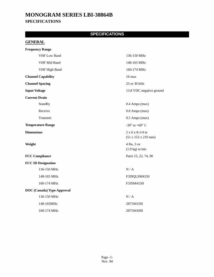
SPECIFICATIONS
GENERAL
Frequency Range
VHF Low Band 136-150 MHz
VHF Mid Band 148-165 MHz
VHF High Band 160-174 MHz
Channel Capability 16 max
Channel Spacing 25 or 30 kHz
Input Voltage 13.8 VDC negative ground
Current Drain
Standby 0.4 Amps (max)
Receive 0.8 Amps (max)
Transmit 9.5 Amps (max)
Temperature Range -30° to +60° C
Dimensions 2 x 6 x 8-1/4 in(51 x 152 x 210 mm)
Weight 4 lbs, 3 oz
(1.9 kg) w/mic
FCC Compliance Parts 15, 22, 74, 90
FCC ID Designation
136-150 MHz N / A
148-165 MHz F3J9QLSM4150
160-174 MHz F3JSM415H
DOC (Canada) Type Approval
136-150 MHz N / A
148-165MHz 287194150I
160-174 MHz 287194100I
MONOGRAM SERIES LBI-38864BSPECIFICATIONS
Page -1-Nov. 94
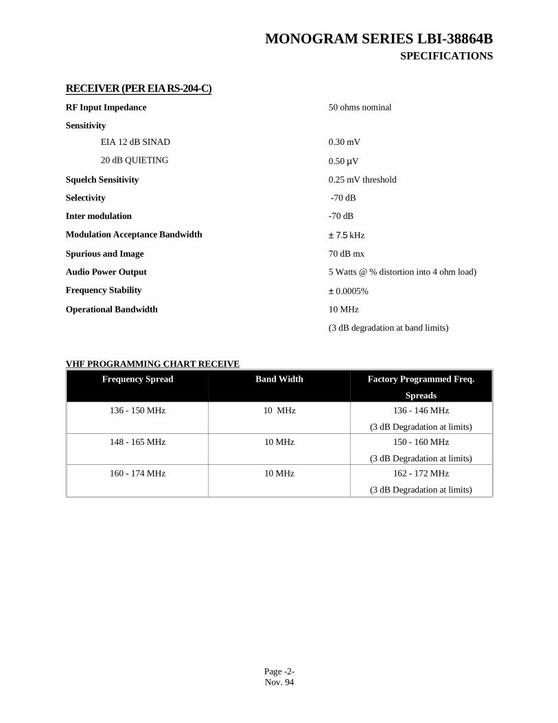
RECEIVER (PER EIA RS-204-C)
RF Input Impedance 50 ohms nominal
Sensitivity
EIA 12 dB SINAD 0.30 mV
20 dB QUIETING 0.50 µV
Squelch Sensitivity 0.25 mV threshold
Selectivity -70 dB
Inter modulation -70 dB
Modulation Acceptance Bandwidth ± 7.5 kHz
Spurious and Image 70 dB mx
Audio Power Output 5 Watts @ % distortion into 4 ohm load)
Frequency Stability ± 0.0005%
Operational Bandwidth 10 MHz
(3 dB degradation at band limits)
Frequency Spread Band Width Factory Programmed Freq.
Spreads
136 - 150 MHz 10 MHz 136 - 146 MHz
(3 dB Degradation at limits)
148 - 165 MHz 10 MHz 150 - 160 MHz
(3 dB Degradation at limits)
160 - 174 MHz 10 MHz 162 - 172 MHz
(3 dB Degradation at limits)
VHF PROGRAMMING CHART RECEIVE
MONOGRAM SERIES LBI-38864BSPECIFICATIONS
Page -2-Nov. 94

TRANSMITTER (PER EIA RS-152-B)
RF Power Output 40 W (adjustable)
RF Output Impedance 50 ohms
Spurious and Harmonics -70 dBc
Modulation 16 K0F3E
FM Hum and Noise -45dB nominal
Audio Distortion < 3 % @ 1000 Hz
Frequency Stability ± 0.0005%
Operational Bandwidth 10 MHz
(3 dB degradation at band limits)
Frequency Spread Band Width Factory Programmed Freq.
Spreads
136 - 150 MHz 10 MHz 136 - 146 MHz
(3 dB Degradation at limits)
148 - 165 MHz 10 MHz 150 - 160 MHz
(3 dB Degradation at limits)
160 - 174 MHz 10 MHz 162 - 172 MHz
(3 dB Degradation at limits)
VHF PROGRAMMING CHART TRANSMIT
MONOGRAM SERIES LBI-38864BSPECIFICATIONS
Page -3-Nov. 94

OPTIONS AND ACCESSORIES
CONTROL STATION OPTIONS:
NOT SHOWN:
Antenna - MGAN1A
Relay Kit - MGSU1C
Noise Suppression Kit - MGPD1A
External Speaker MGZM7C
Desk Microphone MGMC5H
Power Supply MGPS5V
MONOGRAM SERIES LBI-38864BSPECIFICATIONS
Page -4-Nov. 94

UNPACKING
FIGURE 1 - Unpacking Diagram
Check the carton and packing material carefully for the following items:
1. Transceiver Unit
2. Microphone
3. DC power Cord
4. Mobile Mounting Bracket
5. Assembly Hardware
6. Operating GuideStyrofoam not used Inner packing is now cardboard tray box.
MONOGRAM SERIES LBI-38864BUNPACKING
Page -5-Nov. 94

GENERAL DESCRIPTION
Introduction
The Conventional Monogram Series Radio is a rugged, two-way FM mobile radio which operates in either the148-165 MHz band split or the 160-174 MHz band split. The Monogram is a synthesized radio utilizingmicrocomputer technology to provide reliable high-quality simplex two-way mobile communications. Its transmitteroutput power level is 40 watts over the wide bandwidth, with an allowable 10 MHz maximum receive channelseparation. The basic radio package includes the following features:
Features
∗ Microprocessor Control
∗ Synthesized RF Channel Selection (Frequency Control)
∗ Vacuum Fluorescent Channel Selection Display
∗ Channel Guard (CTCSS) Enclode/Decode
∗ Digital Channel Guard (DCS Encode/Decode)
∗ Priority Scan
∗ ± 5 PPM Frequency Stability
∗ Field Programmable with PC
∗ Variable Squelch
∗ Internal 5-watt Speaker, with Volume Control
∗ Side Mounted Microphone Connector
∗ Rear Mounted Antenna Connector (SO-239)
∗ Rear Power Connections
The small size of the Monogram radio makes it ideal for front mounting in conventional vehicles. The radio isoperated with a simple hand-held microphone in combination with the operating controls described in the followingsection.
MONOGRAM SERIES LBI-38864BGENERAL DESCRIPTION
Page -6-Nov. 94
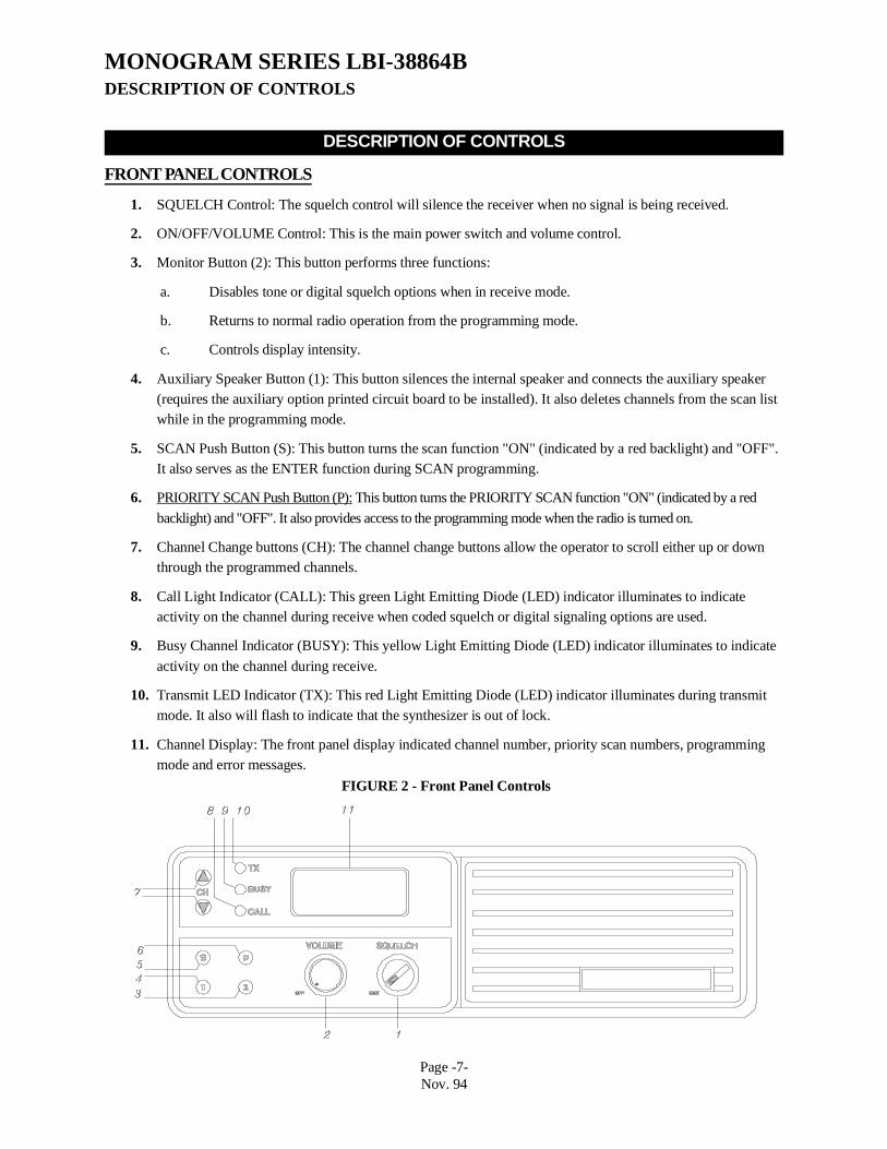
DESCRIPTION OF CONTROLS
FRONT PANEL CONTROLS
1. SQUELCH Control: The squelch control will silence the receiver when no signal is being received.
2. ON/OFF/VOLUME Control: This is the main power switch and volume control.
3. Monitor Button (2): This button performs three functions:
a. Disables tone or digital squelch options when in receive mode.
b. Returns to normal radio operation from the programming mode.
c. Controls display intensity.
4. Auxiliary Speaker Button (1): This button silences the internal speaker and connects the auxiliary speaker(requires the auxiliary option printed circuit board to be installed). It also deletes channels from the scan listwhile in the programming mode.
5. SCAN Push Button (S): This button turns the scan function "ON" (indicated by a red backlight) and "OFF".It also serves as the ENTER function during SCAN programming.
6. PRIORITY SCAN Push Button (P): This button turns the PRIORITY SCAN function "ON" (indicated by a red
backlight) and "OFF". It also provides access to the programming mode when the radio is turned on.
7. Channel Change buttons (CH): The channel change buttons allow the operator to scroll either up or downthrough the programmed channels.
8. Call Light Indicator (CALL): This green Light Emitting Diode (LED) indicator illuminates to indicateactivity on the channel during receive when coded squelch or digital signaling options are used.
9. Busy Channel Indicator (BUSY): This yellow Light Emitting Diode (LED) indicator illuminates to indicate
activity on the channel during receive.
10. Transmit LED Indicator (TX): This red Light Emitting Diode (LED) indicator illuminates during transmitmode. It also will flash to indicate that the synthesizer is out of lock.
11. Channel Display: The front panel display indicated channel number, priority scan numbers, programmingmode and error messages.
FIGURE 2 - Front Panel Controls
MONOGRAM SERIES LBI-38864BDESCRIPTION OF CONTROLS
Page -7-Nov. 94
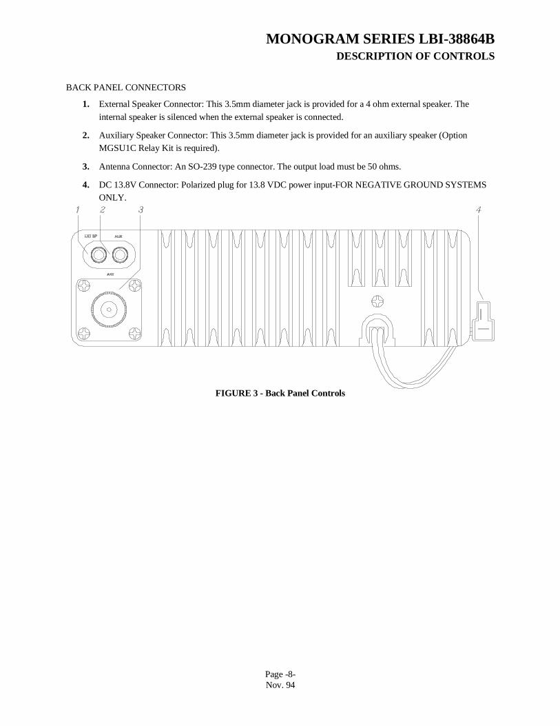
BACK PANEL CONNECTORS
1. External Speaker Connector: This 3.5mm diameter jack is provided for a 4 ohm external speaker. The
internal speaker is silenced when the external speaker is connected.
2. Auxiliary Speaker Connector: This 3.5mm diameter jack is provided for an auxiliary speaker (OptionMGSU1C Relay Kit is required).
3. Antenna Connector: An SO-239 type connector. The output load must be 50 ohms.
4. DC 13.8V Connector: Polarized plug for 13.8 VDC power input-FOR NEGATIVE GROUND SYSTEMSONLY.
FIGURE 3 - Back Panel Controls
MONOGRAM SERIES LBI-38864BDESCRIPTION OF CONTROLS
Page -8-Nov. 94
GENERAL OPERATION
• NOTE: The following description briefly outlines the operation of your VHF synthesized mobile radio. Consultthe operator’s manual for a complete description of all the modes of operation.
RADIO ON/OFF, POWER UP
1. Turn the radio on by turning the VOLUME control one-half turn clockwise. After "4000" appears in thedisplay and the power up alert tone is generated, the display will change to the #1 priority channel. If nopriority channel has been programmed, the display will change to channel 1.
2. Turn the radio off by rotating the VOLUME control fully counter-clockwise.
RECEIVING
1. Turn the radio on and select the desired channel.
2. Depress the MONITOR button (2) if necessary to illuminate it’s backlight. Adjust the volume control to acomfortable listening level.
3. Rotate the SQUELCH control clockwise until the squelch noise (rushing sound) is no longer present.
4. Depress the MONITOR button (2) to extinguish the black light.
• NOTE: If the radio is equipped with coded squelch options, depress the MONITOR button (2) to enable theoption; the CALL indicator will no longer be illuminated.
TRANSMITTING
1. Turn the radio on and select the desired channel.
2. Pick up the microphone and listen briefly to insure the channel is clear. Alternatively, leave the microphone
on-hook and depress the MONITOR button (2).
3. Depress the PTT switch on the side of the microphone. Hold the microphone one to two inches from themouth and speak in a normal tone of voice. The TX indicator should be illuminated.
4. Release the PTT switch when the message is completed.
MONOGRAM SERIES LBI-38864BGENERAL OPERATION
Page -9-Nov. 94

DIGITAL CHANNEL GUARD
Channel Guard provides a means of restricting calls to specific radios through the use of a CTCSS (Continuous ToneCoded Squelch) or DCS (Digitally Coded Squelch). The tone frequencies range from 67 Hz to 250.3 Hz and thereare 83 programable codes.
Channel Guard tone frequencies and codes are software programmable. Both tone frequencies and digital codes maybe mixed on each channel. The frequencies and codes are shown in Tables 1 and 2. A Channel Number display thatdoes not flash, indicates that Channel Guard is not programmed. A flashing Channel Number indicates that ChannelGuard is programmed and disabled.
Table 1 - Channel Guard Tone Frequencies
Standard Tone Frequencies in Hertz67.0 71.9 74.4 77.0 79.7 82.5 85.4 88.5
91.5 94.8 97.4 100.0 103.5 107.2 110.9 114.8
118.8 123.0 127.3 131.8 136.5 141.3 146.2 151.4
156.7 162.2 167.9 173.8 179.9 186.2 192.8 203.5
210.7 218.1 225.7 233.6 241.8 250.3
Digital Squelch Codes023 114 174 266 411 506 703
025 115 205 271 412 516 712
026 116 212 274 413 523 723
031 122 223 306 423 526 731
032 125 225 311 431 532 732
036 131 226 315 432 546 734
043 132 243 325 445 565 743
047 134 244 331 446 606 754
051 143 245 332 452 612
053 145 246 343 454 624
054 152 251 346 455 627
065 155 252 351 462 631
071 156 255 356 464 632
072 162 261 364 465 654
073 165 263 365 466 662
074 172 265 371 503 664
Table 2 - Primary DCS Codes
MONOGRAM SERIES LBI-38864BGENERAL OPERATION
Page -10-Nov. 94

CIRCUIT ANALYSIS
RECEIVER
RF Amplifier
Incoming signals from the antenna jack are routed backwards through the transmitter lowpass filter in PIN diodeswitch D12. In receive mode, D12 conducts allowing a low impedance path through the diode to the receiver frontend circuitry. The receiver RF amplifier section is comprised of two bandpass filter sections separated by anamplifier based around Q1. These two filters allow signals at or near the operating frequency to pass but providestrong rejection of the mixer’s spurious response frequencies. The first filter section is a two pole design formedaround RF transformers T1, T2 and their associated circuitry. This filter is followed by the RF amplifier transistorQ1. This device is a dual-gate MOSFET which, with its low noise figure, yields good receiver sensitivity whileshowing strong resistance to overload from strong signals. The output of Q1 drives a three-pole filter section formedaround T3, T4 and T5. The output of the RF amplifier stage is routed to the first mixer.
First Mixer and First IF Amplifier
The action of the first mixer transistor Q2 is to convert incoming signals at the operating frequency to the frequencyof the first IF which is 21.4 MHz. The output of the mixer is at a frequency which is equal to the difference betweenthe frequency of the incoming signal and the local oscillator. In this radio, the local oscillator signal is chosen to be21.4 MHz below the operating frequency. The device chosen to perform the mixing operation is Q2, a highperformance JFET. The incoming signal is applied to the gate of Q2, and the local oscillator signal is filtered bytransformers T6, T7 and associated circuitry before being supplied to the drain of Q2. The difference frequencysignal at 21.4 MHz exits the mixer at the source of Q2 drives the first IF filter XF1 and XF2. XF1 and XF2 form a4-pole monolithic crystal filter pair which in part determines the selectivity of the radio. The output of the crystalfilter is routed to the first IF amplifier formed around Q3. RF transformer T8 and T9 provide proper matching of thecrystal filters to insure good pass band response and selectivity.
Second Mixer, Second IF, and FM Detector
The output of Q3 is applied to the input (pin 16) of IC2. IC2 is a single conversion FM receiver on one integratedcircuit chip. The signal at the input is routed straight to a mixer which converts the incoming signal to the second IFfrequency of 455 kHz. The second local oscillator is formed with crystal X1 and circuitry within IC2. The output ofthe second mixer is at pin 23 which is connected to a ceramic bandpass filter CF1 and centered at 455 kHz. Thisfilter, along with XF1 and XF2, determine the adjacent channel selectivity of the radio. The output of CF1 drives ahigh gain IF amplifier chain internal to IC2 which in turn drives the quadrature detector. The output of the detector isamplified and exits IC2 at pin 9.
Audio
Detected audio from IC2 passes through a lowpass filter formed around L7, C53 and C52 which removes IFfrequency components at 455 kHz. The audio signal then passes through buffer amplifier transistor Q6 before beingfiltered by a two section, 4-pole high pass filter (IC3) This filter removes DCS and CTCSS low frequency tonesfrom the recovered audio. Transistors Q7 and Q8 act as switches around volume control VR2 to mute the audioduring squelched receive operation. The audio signal is finally routed to audio power amplifier IC5 and then to thespeaker.
MONOGRAM SERIES LBI-38864BCIRCUIT ANALYSIS
Page -11-Nov. 94

Squelch
The presence of an RF carrier is determined by noting the level of ultrasonic noise at the detector output (pin 9) ofIC2. When a carrier is present, the noise level drops. The audio at pin 9 of IC2 is filtered by a two-pole bandpassfilter formed around L5, L6 C48 and C50. This filter passes at and near an audio frequency of 50 kHz. Thisfrequency is high enough that voice audio and its harmonics will not cause improper squelch operation. The outputof the filter is routed to an amplifier internal to IC2. The output of the amplifier drives the squelch detector D7 andD8. The DC voltage at the detector output is amplified and filtered by Q4. The output of Q4 sends its squelch signalto the microprocessor. When the microprocessor determines that a valid carrier exists, it sends an unmute signal tothe audio switch transistors Q7 and Q8.
TRANSMITTER
Audio
The microphone audio is amplified, pre-emphasized and peak limited by circuits within IC113. The output of thelimiter is routed through RV4, the microphone; deviation control. Input CTCSS and routed DCS signals are routedthrough RV5, the CTCSS/DCS deviation control. Both signals are summed and lowpass filtered to remove highfrequency components from the limiter which could cause channel splatter. When the microprocessor enables the TX8 Volt supply, analog gate IC115 delivers the modulation signal to the VCO transistor Q112.
RF Driver and Power Amplifier
Diode D9 acts as a switch allowing the RF signal from the phase locked loop frequency synthesizer to pass throughto the RF driver and power amplifier during receive. Buffer amplifier Q9 amplifies the carrier to the level needed bythe driver amplifier stages. The driver amplifiers, of which the last 2 stages are gain controlled by the automaticpower control, drive the final amplifier stage formed around Q12. The final amplifier boosts the carrier level to thepower level set by the automatic power control. The carrier signal passes through the automatic power controldirectional coupler, the RF output lowpass filter, and then is routed to the antenna connector.
Automatic Power Control
The automatic power control directional coupler samples a portion of the forward RF power output to determine theRF level. Diode D10 rectifies this RF sample and produces a DC voltage which is proportional to the RF outputlevel. This DC signal is summed with the voltage set from the power output control RV2. This voltage is comparedwith a voltage derived from the TX 8 Volt supply and the difference is amplified by IC4. The output is furtheramplified by Q14 and Q13. The output voltage on Q13 is the supply voltage for the RF driver stage. The output ofthe RF driver is proportional to its supply voltage. This completes a negative feedback loop which results in constantoutput power over supply voltage and temperature variations.
FREQUENCY SYNTHESIZER
The phase locked loop (PLL) frequency synthesizer section is responsible for generating the RF signal at the carrierfrequency during transmit and at the local oscillator frequency for the receiver during receive. A PLL functions bycomparing the output frequency of a voltage controlled oscillator (VCO) with a fixed frequency reference. An errorsignal is generated which drives the control input of the voltage controlled oscillator to force its frequency to matchthe reference. The PLL based frequency synthesizer has a digital frequency divider inserted between the output ofthe VCO and the frequency comparison circuitry. As this divider number is varied, the output frequency of the VCOvaries as well with a frequency step size equal to the reference frequency (5 kHz in this radio). This allows a largerange of frequencies to be generated with one well controlled oscillator signal, the reference.
PLL Integrated circuit
IC108 contains most of the digital circuitry to form a PLL frequency synthesizer. This includes a reference oscillator,programmable variable frequency divider, a modulus control counter, a phase/frequency comparator and a frequencylock dector. The operation of this integrated circuit is controlled by the radio’s microprocessor through a serial dataline.
MONOGRAM SERIES LBI-38864BCIRCUIT ANALYSIS
Page -12-Nov. 94

Reference Oscillator
Crystal X3, varactor diode D119, a thermistor/resistor network and oscillator stage of IC108 from a temperaturecompensated 10.24 MHz oscillator. This frequency is divided by 2084 to generate the 5 kHz reference frequency forthe PLL frequency synthesizer. This reference determines the frequency stability of the overall radio.
Voltage Controlled Oscillator
FET transistor Q112 and its associated circuitry form a grounded gate oscillator which is voltage tuned by varactordiodes D120 and D121 and which is bandswitched by diodes D122 and D123 (D126 and D127 for Low band). TheVCO output is buffered and isolated by Q113, Q114 and Q119. Audio modulation is applied to the source of Q112to produce frequency modulation during transmit.
Dual Modulus Prescaler
The internal dividers within IC108 are not able to operate at the VCO output frequency. To alleviate this problem,part of the overall frequency division necessary between the VCO and the phase/frequency comparator is placedexternal to, and controlled by, IC108. IC109 divides the VCO frequency by 64 or 65, determined by the state ofIC108 pin 6. This produces a lower frequency which can be further divided by IC108. By strategic timing when todivide by 64 or 65, the overall division will be that necessary to put the VCO on the correct frequency.
Loop Filter
Resistors R316, R323, R324, R325, R326 and capacitors C263, C264 and C265 form the loop filter. The purpose ofthe loop filter is to filter out the 5 kHz reference frequency products from the output of phase/frequency comparatorIC108 and to determine the dynamic operation of the overall loop.
R315, C262, Q107 and Q108 act to speed up operation of the synthesizer loop during channel changes and duringfrequency transition (receive to transmit and transmit to receive).
Out-Of-Lock Detector
IC108 contains a circuit which compares the timing difference of the 5 kHz reference frequency and the divideddown VCO frequency. The output is a 5 kHz pulse whose duration is equal to the timing difference. R312 and C295filter this pulse and average it producing a DC voltage which is proportional to the pulse width. When the loop is inlock, this voltage is zero, but when the loop is in lock, this voltage is zero, but when the loop is out of lock, it rises toa level which will forward bias Q106. The output of Q106 drives the microprocessor. The microprocessor will notallow the radio to transmit unless the synthesizer is in lock. This is to prevent out of band signals from beingtransmitted.
MONOGRAM SERIES LBI-38864BCIRCUIT ANALYSIS
Page -13-Nov. 94

PREVENTIVE MAINTENANCE
To ensure high operating efficiency and to prevent mechanical and electrical failures from interrupting systemoperations, routing checks should be made of all mechanical and electrical parts at regular intervals. Preventivemaintenance should include the following checks:
CONNECTIONS
Ground connections to the voltage source should be periodically checked for tightness. Loose or poor connections tothe power source will cause excessive voltage drops and faulty operation. When ground connections are not madedirectly to the battery, the connection from the battery to vehicle chassis must be checked for low impedance. A highimpedance may cause excessive voltage drops and alternator noise problems.
ELECTRICAL SYSTEM
Check the voltage regulator and alternator or generator periodically to keep the electrical system within safe andeconomical operation limits. Over voltage is indicated when the battery loses water rapidly. Usage of 1 or 2 ouncesof water per cell per week is acceptable for batteries in continuous operation. A weak battery will often causeexcessive noise or faulty operation.
MECHANICAL INSPECTION
Since mobile units are subject to constant shock and vibration, check for loose plugs, nuts, screws and other parts tomake sure that nothing is working loose.
ANTENNA
The antenna, antenna base and all contacts should be kept clean and free from corrosion. If the antenna or its baseshould become coated or poorly grounded, loss of radiation and a weak signal will result.
ALIGNMENT
The transmitter and receiver meter readings should be checked periodically, and the alignment "touched up" whennecessary. Refer to the Alignment Procedure in this Service Manual.
FREQUENCY CHECK
Check the transmitter frequency and deviation. Normally, these checks are made when the unit is first put intooperation, after the first six months, and once a year thereafter.
MONOGRAM SERIES LBI-38864BPREVENTIVE MAINTENANCE
Page -14-Nov. 94

DISASSEMBLY
TOP AND BOTTOM COVERS
There are no screws used to secure the top and bottom covers. Both top and bottom covers are removedwith a flat blade screwdriver or similar tool. On each side of the radio there are two small slots (one at thetop and one at the bottom). Insert the screwdriver into the slot and gently pry the lip of the cover out fromthe radio. Without removing the screwdriver from the slot and in the same motion, pry the cover up. Bothcovers can be removed from either side of the radio.
FRONT PANEL
1. Remove the (6) M3 x 6 machine screws (3 on top and 3 on bottom) that secure the Front Panel to thechassis.
2. Two cables connect the Control Board to the RF Board (at PL1) and to the Digital Board (at PL2). Thesecables may be unplugged at the RF Board and at the Digital Board. A ribbon cable from the Display Boardis connected to the Digital Board (at FLT) and may be unplugged to remove it.
RF BOARD
• NOTE: Any reference to item’s in the following disassembly procedure pertain to the Exploded View PartsBreakdown page.
1. Remove the (13) M3 x 24 machine screws securing the RF shield to the chassis.
2. Remove the M3 x 8 machine screw that secure the DC Cord bracket to the chassis. Slide the bracket andcord out of the chassis.
3. Remove the (6) M3 x 6 machine screws (3 on top and 3 on bottom) that secure the Front Panel to the
chassis.
4. Remove the RF shield by pushing the Front Panel forward so the shield will clear and then sliding the DCCord, bracket and connector through the rectangular hole in the shield.
5. De-solder the antenna connector from the RF Board.
6. Remove the remaining (11) machine screws securing RF Board, IC1, Q11 and Q13.
7. Unplug the VCO cable from the jack and remove the RF Board
MONOGRAM SERIES LBI-38864BDISASSEMBLY
Page -15-Nov. 94

DIGITAL BOARD
1. Remove the (6) M3 x 18 machine screws that secure the Top Panel shield to the chassis.
2. Unplug and remove the Auxillary Relay P.C.B. at PL5.
3. Remove the (6) machine screws (3 on top and 3 on bottom) that secure the Front Panel to the chassis.
• The following steps detail the removal of the RF shield which is necessary before continuing with the removalof the Digital Board.
4. Remove the (13) M3 x 24 machine screws securing the RF shield to the chassis.
5. Remove the M3 x 8 machine screw that secure the DC Cord bracket to the chassis. Slide the bracket andcord out of the chassis.
6. Remove the RF shield by pushing the Front Panel forward so the shield will clear and then sliding the DCCord, bracket and connector through the rectangular hole in the shield.
7. Unplug the VCO cable from the jack.
8. Remove the remaining (10) screws securing the Digital Board, IC5, IC6 and IC104 to the chassis.
9. The Digital Board can now be removed from the chassis, however the Front Panel assembly is still attached by
two cables (one from the Control board and one from the Display board). The cable from the Control Board at PL2may be unplugged. The ribbon cable from Digital Board may be unplugged at FLT.
MONOGRAM SERIES LBI-38864BDISASSEMBLY
Page -16-Nov. 94

PROGRAMMING INSTRUCTIONS
The VHF synthesized mobile radio is equipped with a personality EEPROM. All customer informationsuch as the customer frequencies, customer tones and customer options are stored in the EEPROM. TheEEPROM contains all information to tailor the operation of the radio to the user’s requirements. TheEEPROM is programmed by using an IBM compatible personal computer with MSDOS, ProgrammingCable TQ-3376 and Programming software TQ-3375.
PROGRAMMING THE RADIO
The programming Cable TQ-3376 is a Y-cable. The base of the "Y" has a standard 25 pin connector which plugsinto the computer, the remaining end has a 6 pin connector which fits into the connector PL1 on the digital boardinside the radio. To use this cable, remove the top cover of the radio as described in the DISAASSEMBLY section.Plug the 6 pin connector into the socket inside the radio (PL1), which is located near the EEPROM IC107. Plug thebase of the "Y" into the computer that will program the radio. See the diagram in TQ-3375 Software Manual. Inorder to program the radio with the programming cable, it is necessary to put the radio into the programming mode.To do this, press the P "Priority" button/LED on the radio and turn the radio ON. The radio will sound a prompttone and show the words "PROG" on the display. Please refer to the Software Manual for further instructions on theoperation of the Programming Software. After completing the programming instructions in the Manual, remove thecable from PL1 and replace the cover on your VHF synthesized mobile radio.
MONOGRAM SERIES LBI-38864BPROGRAMMING INSTRUCTIONS
Page -17-Nov. 94

TEST EQUIPMENT SETUP
Figure 4 - Test Equipment Setup
* Optional Test Equipment
*
*
MONOGRAM SERIES LBI-38864BTEST EQUIPMENT SETUP
Page -18-Nov. 94
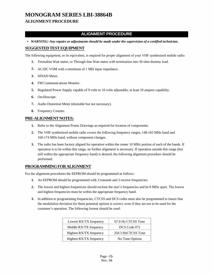
ALIGNMENT PROCEDURE
• WARNING: Any repairs or adjustments should be made under the supervision of a certified technician.
SUGGESTED TEST EQUIPMENT
The following equipment, or its equivalent, is required for proper alignment of your VHF synthesized mobile radio:
1. Termaline Watt meter, or Through-line Watt meter with termination into 50 ohm dummy load.
2. AC/DC VOM with a minimum of 1 MΩ input impedance.
3. SINAD Meter.
4. FM Communications Monitor.
5. Regulated Power Supply capable of 9 volts to 16 volts adjustable; at least 10 ampere capability.
6. Oscilloscope.
7. Audio Distortion Meter (desirable but not necessary).
8. Frequency Counter.
PRE-ALIGNMENT NOTES:
1. Refer to the Alignment Points Drawings as required for location of components.
2. The VHF synthesized mobile radio covers the following frequency ranges, 148-165 MHz band and
160-174 MHz band, without component changes.
3. The radio has been factory aligned for operation within the center 10 MHz portion of each of the bands. Ifoperation is to be within this range, no further alignment is necessary. If operation outside this range (but
still within the appropriate frequency band) is desired, the following alignment procedure should beperformed.
PROGRAMMING FOR ALIGNMENT
For the alignment procedures the EEPROM should be programmed as follows:
1. An EEPROM should be programmed with 3 transmit and 3 receive frequencies.
2. The lowest and highest frequencies should enclose the user’s frequencies and be 8 MHz apart. The lowestand highest frequencies must be within the appropriate frequency band.
3. In addition to programming frequencies, CTCSS and DCS codes must also be programmed to insure thatthe modulation deviation for these potential options is correct, even if they are not to be used for thecustomer’s operation. The following format should be used:
Lowest RX/TX frequency 67.0 Hz CTCSS Tone
Middle RX/TX frequency DCS Code 072
Highest RX/TX frequency 250.3 HzCTCSS Tone
Highest RX/TX frequency No Tone Options
MONOGRAM SERIES LBI-38864BALIGNMENT PROCEDURE
Page -19-Nov. 94
4. The middle RX/TX frequencies should be halfway between the lowest and the highest frequencies.
• NOTE: There should be 4 channels programmed with a total of 3 different frequencies.
PLL ALIGNMENT
1. Connect an RF dummy load or power attenuator (50 watt minimum rating) to the antenna connector.
2. Connect a VOM or DVM to TP1, accessed through a hole in the VCO cover.
3. Set the CHANNEL selector to the highest transmit frequency.
4. Press the push-to-talk (PTT) switch. Adjust TC5 for a 7.0 VDC reading on the VOM. Release the PTTswitch.
5. Change the CHANNEL selector to the lowest transmit frequency.
6. Press the PTT switch. The VOM should read 1.5 VDC ± 0.2V VDC. If not, re-adjust TC5 slightly for a 1.5VDC reading. Release the PTT switch.
7. Return to the highest transmit channel and verify that the TP1 voltage does not exceed 8 volts in transmit.
On the lowest transmit frequency, the voltage must be 1.5 ± 0.2 VDC, and on the highest transmitfrequency, the voltage must be less than 7.5 VDC. Repeat steps 3 through 6 if necessary.
8. Set the CHANNEL selector to the lowest receive frequency.
9. Adjust TC3 to obtain a 2 VDC reading on the VOM.
10. Change the CHANNEL selector to the highest receive frequency. Verify that the DC voltage does notexceed 7.0 VDC. If it does, re-adjust TC3 for a 7.0 VDC reading.
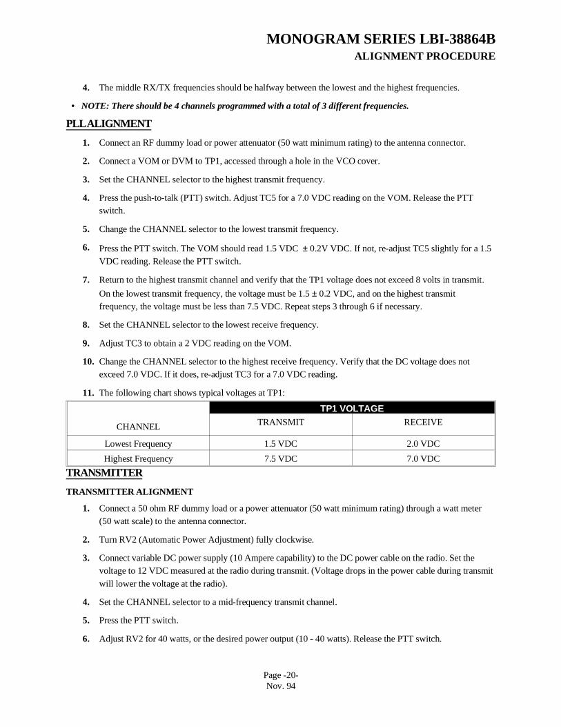
11. The following chart shows typical voltages at TP1:
CHANNEL
TP1 VOLTAGETRANSMIT RECEIVE
Lowest Frequency 1.5 VDC 2.0 VDC
Highest Frequency 7.5 VDC 7.0 VDC
TRANSMITTER
TRANSMITTER ALIGNMENT
1. Connect a 50 ohm RF dummy load or a power attenuator (50 watt minimum rating) through a watt meter(50 watt scale) to the antenna connector.
2. Turn RV2 (Automatic Power Adjustment) fully clockwise.
3. Connect variable DC power supply (10 Ampere capability) to the DC power cable on the radio. Set thevoltage to 12 VDC measured at the radio during transmit. (Voltage drops in the power cable during transmit
will lower the voltage at the radio).
4. Set the CHANNEL selector to a mid-frequency transmit channel.
5. Press the PTT switch.
6. Adjust RV2 for 40 watts, or the desired power output (10 - 40 watts). Release the PTT switch.
MONOGRAM SERIES LBI-38864BALIGNMENT PROCEDURE
Page -20-Nov. 94
• WARNING: To prevent damage to the radio, avoid keying the radio for periods longer than 1 minute. Allow a5 minute cool down period after keying the radio for 1 minute.
7. Repeat step 6 above for the lowest, middle, and highest frequency transmit channel with the goal to achievethe least variation in power output across the band.
8. Increase the power supply voltage to 13.8 VDC measured at the radio during transmit.
DCS Modulation Balance Adjustment
1. Connect test equipment to the radio as shown in Figure 4.
2. Set the CHANNEL selector to a transmit channel which has a DCS code pre-programmed (should be
mid-frequency channel).
• WARNING: The power attenuator must have enough attenuation to prevent damage to the Deviation Meter.
3. Press the PTT switch.
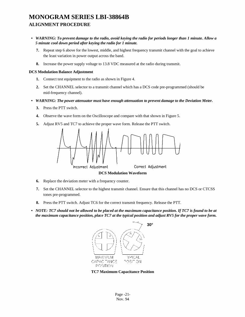
4. Observe the wave form on the Oscilloscope and compare with that shown in Figure 5.
5. Adjust RV5 and TC7 to achieve the proper wave form. Release the PTT switch.
DCS Modulation Waveform
6. Replace the deviation meter with a frequency counter.
7. Set the CHANNEL selector to the highest transmit channel. Ensure that this channel has no DCS or CTCSStones pre-programmed.
8. Press the PTT switch. Adjust TC6 for the correct transmit frequency. Release the PTT.
• NOTE: TC7 should not be allowed to be placed at the maximum capacitance position. If TC7 is found to be atthe maximum capacitance position, place TC7 at the typical position and adjust RV5 for the proper wave form.
30°
TC7 Maximum Capacitance Position
MONOGRAM SERIES LBI-38864BALIGNMENT PROCEDURE
Page -21-Nov. 94

Modulation Deviation Adjustment
1. Connect an RF deviation meter to the radio through a power attenuator.
2. Set the CHANNEL selector to a transmit channel which has a DCS code pre-programmed (should be a
mid-frequency channel).
3. Press the PTT switch.
4. Adjust RV3 for proper deviation, typically 750 Hz. Release the PTT switch.
5. Set the CHANNEL selector to a transmit channel which has a low-frequency CTCSS tone (67.0Hz)preprogrammed.
6. Press the PTT switch and verify that the deviation is between 500 Hz and 1000 Hz. Release the PTT switch.
7. Set the CHANNEL selector to a transmit channel which has a high-frequency CTCSS tone (250.3 Hz)preprogrammed.
8. Press the PTT switch and verify that the deviation is between 500 Hz and 1000 Hz. Release the PTT switch.
If deviation is above or below 500-1000 Hz, adjust RV 401 (filter) to same level as obtained in Step 6.
9. Connect an audio frequency generator to the MIC input (connected to the white wire in the microphonecable) of the radio. Set the audio output level for 30 mV. The audio frequency should be 1 kHz.
10. Press the PTT switch.
11. Adjust RV4 (Maximum Deviation Adjustment) for the 4.2 kHz deviation if no CTCSS tones are present,
and 4.8 kHz deviation if CTCSS tones are present.
RECEIVER ALIGNMENT
1. Connect an RF signal generator or communications service monitor to the antenna connector.
2. Connect a SINAD meter and an audio distortion analyzer across the speaker terminals. If an audio
distortion analyzer is not available, connect an oscilloscope across the speaker terminals.
3. Turn the SQUELCH control fully counter-clockwise.
4. Adjust the VOLUME control to the proper level for the sinad meter and audio distortion analyzer.
5. Set the CHANNEL selector to a mid-frequency receive channel.
6. Tune the RF signal generator to the channel frequency. The RF output level should be set for 47 dBm. The
modulation should be set for ± 3 kHz FM deviation of a 1 kHz tone.
7. Adjust T10 for maximum audio output. Readjust the VOLUME control if necessary to avoid clipping on
the output audio wave form. (This adjustment is typically not required.)
8. Decrease the RF generator output and adjust T1 through T5 for maximum sensitivity.
• NOTE: During this adjustment signal generator level should be reduced periodically to keep the Sinad meterreading near 12 dB.
MONOGRAM SERIES LBI-38864BALIGNMENT PROCEDURE
Page -22-Nov. 94
9. Adjust T6 and T7 for maximum sensitivity. These adjustments have a very broad range where little changein sensitivity is noted while the adjustment is being made. The slugs should be set in the middle of this
range.
10. Check the sensitivity at the lowest and highest receive frequencies. If necessary, repeat steps (8) and (9)above at the lowest middle and highest frequencies for the best overall sensitivity.
Receiver Squelch Adjustment
1. Set the channel selector for the mid-frequency receive channel.
2. Connect an RF signal generator or communications service monitor to the antenna connector. The
modulation should be set for ± 3 kHz FM modulation of a 1 kHz tone. The RF output level should be at a
minimum.
3. Adjust the squelch control to the threshold point (the point where the speaker audio disappears).
4. Increase the RF signal generator output level until speaker audio output reappears. Note the generator level.
5. Turn the SQUELCH control fully clockwise.
6. Increase the RF signal generator level by 16 dB.
7. Adjust RV1 until the squelch is again at threshold.
• NOTE: This squelch adjustment procedure is very important for the correct operation of the microprocessoraided squelch system.
MONOGRAM SERIES LBI-38864BALIGNMENT PROCEDURE
Page -23-Nov. 94

ALIGNMENT POINTS 406041-F Issue:H DIGITAL BOARD
MONOGRAM SERIES LBI-38864BALIGNMENT POINTS 406041-F Issue:H DIGITAL BOARD
Page -24-Nov. 94

ALIGNMENT POINTS 406039-E Issue:H RF BOARD
MONOGRAM SERIES LBI-38864BALIGNMENT POINTS 406039-E Issue:H RF BOARD
Page -25-Nov. 94

PERFORMANCE TEST
TRANSMITTER PERFORMANCE TEST
Power Output
1. Set the power supply voltage to 13.8 VDC (measured at the radio during transmit).
2. Connect an RF wattmeter and dummy load to the antenna connector.
3. Press the PTT switch.
4. Verify that the output is at least 40 watts.
5. Reduce the power supply voltage to 11 volts.
6. Verify that the output is at least 15 watts.
7. Release the PTT switch.
Audio Response
1. Connect an audio generator to the microphone jack on the radio. Set the monitor to read average peak FMdeviation.
3. Press the PTT switch.
4. Adjust the audio generator level to produce 1 kHz deviation.
5. Set the audio generator frequency to 500 Hz. The transmitter deviation should decrease to approximately
500 Hz.
6. Set the audio generator frequency to 2 kHz. The transmitter deviation should be approximately 2 kHz.
7. As the audio generator frequency is varied from 300 Hz to 10 kHz, the deviation should increase until it
reaches a maximum at an audio frequency of 2.5 kHz to 2.9 kHz. At higher frequencies, the deviationshould decrease. The deviation at an audio frequency of 6 kHz should be less than 1 kHz.
8. Release the PTT switch.
Limiting Test
1. Set the audio generator frequency to 1 kHz.
2. Press the PTT switch and adjust the generator level to produce 3 kHz deviation. Note the generator level.
3. Increase the audio generator level by 20 dB.
4. Sweep the audio generator over a frequency range of 300 Hz to 3 kHz. The deviation should not exceed
± 5 KHz within this range.
5. Release the PTT switch.
MONOGRAM SERIES LBI-38864BPERFORMANCE TEST
Page -26-Nov. 94
Spectrum Test
1. Connect a spectrum analyzer to a sampled RF output of the radio.
2. Press the PTT switch. Observe the output spectrum on the spectrum analyzer.
3. All spurious and harmonics should be at least 60 dB below the carrier level.
4. Release the PTT switch.
RECEIVER PERFORMANCE TESTS
SINAD Sensitivity
1. Connect the FM signal generator of communication service monitor to the antenna jack.
2. Connect a SINAD Meter across the speaker leads.
3. Turn the SQUELCH control fully counterclockwise for maximum noise.
4. Adjust the VOLUME control to approximately mid-range.
5. Set the FM signal generator/service monitor to the receive frequency. The modulation should be set for 3kHz deviation of a 1 kHz tone.
6. Adjust the generator RF level so that the SINAD meter reads 12 dB. The signal generator RF level should
be .30 µV or less.
Noise Quieting Sensitivity
1. Connect a VOM to the speaker leads.
2. Turn the SQUELCH control fully counterclockwise for maximum noise.
3. With no RF signal generator or communication service monitor connected to the radio, adjust the
VOLUME control to obtain a noise reading of 1 volt RMS on the VOM.
4. Connect the RF signal generator/service monitor to the radio. Set the RF frequency to the receiverfrequency of the radio and remove any modulation.
5. Adjust the signal generator RF level for a noise reading on the VOM of 0.1 volt RMS. This is the 20 dB
noise quieting point. The RF level should be 0.5 µV or less.
Squelch Sensitivity
1. Set the RF signal generator/service monitor to the receive frequency. Set the modulation to 3 kHz deviationof a 1 kHz audio tone.
2. Reduce the signal generator RF output to zero.
3. Rotate the SQUELCH control clockwise to the point where the speaker noise just goes away.
4. Increase the signal generator/service monitor RF level until the speaker noise returns. This is the threshold
squelch setting. The generator output level should not exceed 0.20 µV.
5. Turn the SQUELCH control to maximum clockwise rotation.
6. Increase the generator output level until the squelch opens (busy LED is on). The output level should be
between 10 and 20 dB (3 to 10 times) above the threshold setting.
MONOGRAM SERIES LBI-38864BPERFORMANCE TEST
Page -27-Nov. 94

Audio Output
1. Increase the RF signal generator/service monitor RF level to 1000 µV.
2. Connect a 4 ohm audio dummy load to the AUXILIARY speaker jack.
3. Connect a true RMS audio volmeter (the audio distortion analyzer may include this function) to the speaker
leads.
4. With a 3 kHz deviation of a 1 kHz tone modulation applied to the signal generator, rotate the VOLUMEcontrol clockwise until the audio distortion is 10% or until the VOLUME control reaches stop, whichever
comes first.
5. The audio voltmeter should read 4.0 volts or greater.
MONOGRAM SERIES LBI-38864BPERFORMANCE TEST
Page -28-Nov. 94

COMPONENT REPLACEMENT
SURFACE MOUNT COMPONENTS
Surface mount components should always be replaced using a temperature controlled soldering system. Thesoldering tools may be either a temperature controlled soldering iron or a temperature controlled hot-air solderingstation. A hot-air system is recommended for the removal of components on the multi-layered boards used in theVHF synthesized mobile radio. With either soldering system, a temperature of 700ø F (371ø C) should bemaintained.
The following procedures outline the removal and replacement of surface mount components. If a hot-air solderingsystem is employed, see the manufacturer’s operating instructions for detailed information on the use of your system.
• CAUTION: Avoid applying heat to the body of any surface mount component using standard soldering methods.Heat should be applied only to the metalized terminals of the components. Hot-air systems do not damage thecomponents since the heat is quickly and evenly distributed to the external surface of the component.
• CAUTION: The CMOS Integrated Circuit devices used in this equipment can be destroyed by static discharges.Before handling one of these devices, service technicians should discharge themselves by touching the case of abench test instrument that has a 3-prong power cord connected to an outlet with a known good earth ground.When soldering or desoldering a CMOS device, the soldering equipment should have a known good earth ground.
SURFACE MOUNT REMOVAL
1. Grip the component with tweezers or small needle nose pliers.
2. Alternately heat the metalized terminal ends of the surface mount component with the soldering iron. If ahot-air system is used, direct the heat to the terminals of the component. Use extreme care with thesoldering equipment to prevent damage to the printed circuit board (PCB) and the surrounding components.
3. When the solder on all terminals is liquefied, gently remove the component. Excessive force may cause thePCB pads to separate from the board if all solder is not completely liquefied.
4. It may be necessary to remove excess solder using a vacuum de-soldering tool or Solder wick . Again, usegreat care when de-soldering or soldering on the printed circuit boards. It may also be necessary to removethe epoxy adhesive that was under the surface mount component and any flux on the printed circuit board.
MONOGRAM SERIES LBI-38864BCOMPONENT REPLACEMENT
Page -29-Nov. 94

SURFACE MOUNT COMPONENT REPLACEMENT
1. "Tin" one terminal end of the new component and the corresponding pad of the PCB. Use as little solder aspossible.
2. Place the component on the PCB pads, observing proper orientation for capacitors, diodes, transistors, etc.
3. Simultaneously touch the "tinned" terminal end and the "tinned" pad with the soldering iron. Slightly pressthe component down on the board as the solder liquefies. Solder all terminals, allowing the component timeto cool between each application of heat. Do not apply heat for an excessive length of time and do not use
excessive solder.
With a hot-air system, apply hot air until all "tinned" areas are melted and the component is seated in place. It maybe necessary to slightly press the component down on the board. Touch-up the soldered connections with a standardsoldering iron if needed. Do not use excessive solder.
• CAUTION: Some chemicals may damage the internal and external plastic parts of the radio.
4. Allow the component and the board to cool and then remove all flux from the area using alcohol or anotherapproved flux remover.
SURFACE MOUNTED INTEGRATED CIRCUIT REPLACEMENT
Soldering and de-soldering techniques of the surface mounted IC’s are similar to the above outlined procedures forthe surface mounted chip components. Use extreme care and observe static precautions when removing or replacingthe defective (or suspect) IC’s. This will prevent any damage to the printed circuit board or the surrounding circuitry.
The hot-air soldering system is the best method of replacing surface mount IC’s. The IC’s can easily be removed andinstalled using the hot-air system. See the manufacturers instructions for complete details on tip selection and otheroperating instructions unique to your system.
If a hot-air system is not available, the service technician may wish to clip the pins near the body of the defective ICand remove it. The pins can then be removed from the PCB with a standard soldering iron and tweezers, and the newIC installed following the Surface Mount Component Replacement procedures. it may not be necessary to "tin" all(or any) of the IC pins before the installation process.
MONOGRAM SERIES LBI-38864BCOMPONENT REPLACEMENT
Page -30-Nov. 94

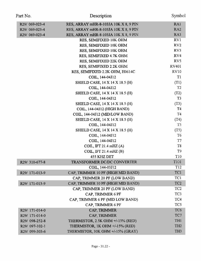
ELECTRICAL PARTS LIST
Only those items indicated by shading will be stocked by After MarketServices. All other items are for reference only.
When ordering parts for your Monogram Series radio, precede all partnumbers with the prefix "R29/"
NOTE
Page -31-Nov. 94

Page - 31.1 -

Page - 31.2 -
Page - 31.3 -

Page - 31.4 -

Page - 31.5 -

Page - 31.6 -
Page - 31.7 -

Page - 31.8 -

Page - 31.9 -

Page - 31.10 -

Page - 31.11 -

Page - 31.12 -
Page - 31.13 -

Page - 31.14 -

Page - 31.15 -

Page - 31.16 -
Page - 31.17 -

Page - 31.18 -

Page - 31.19 -

Page - 31.20 -

Page - 31.21 -
Page - 31.22 -

Page - 31.23 -

Page - 31.24 -

PRINTED CIRCUIT BOARD LAYOUT
Page -32.0-Nov. 94

TOP VIEW 406041-F ISSUE: H / DIGITAL BOARD
MONOGRAM SERIES LBI-38864BTOP VIEW 406041-F ISSUE: H / DIGITAL BOARD
Page -32.1-Nov. 94
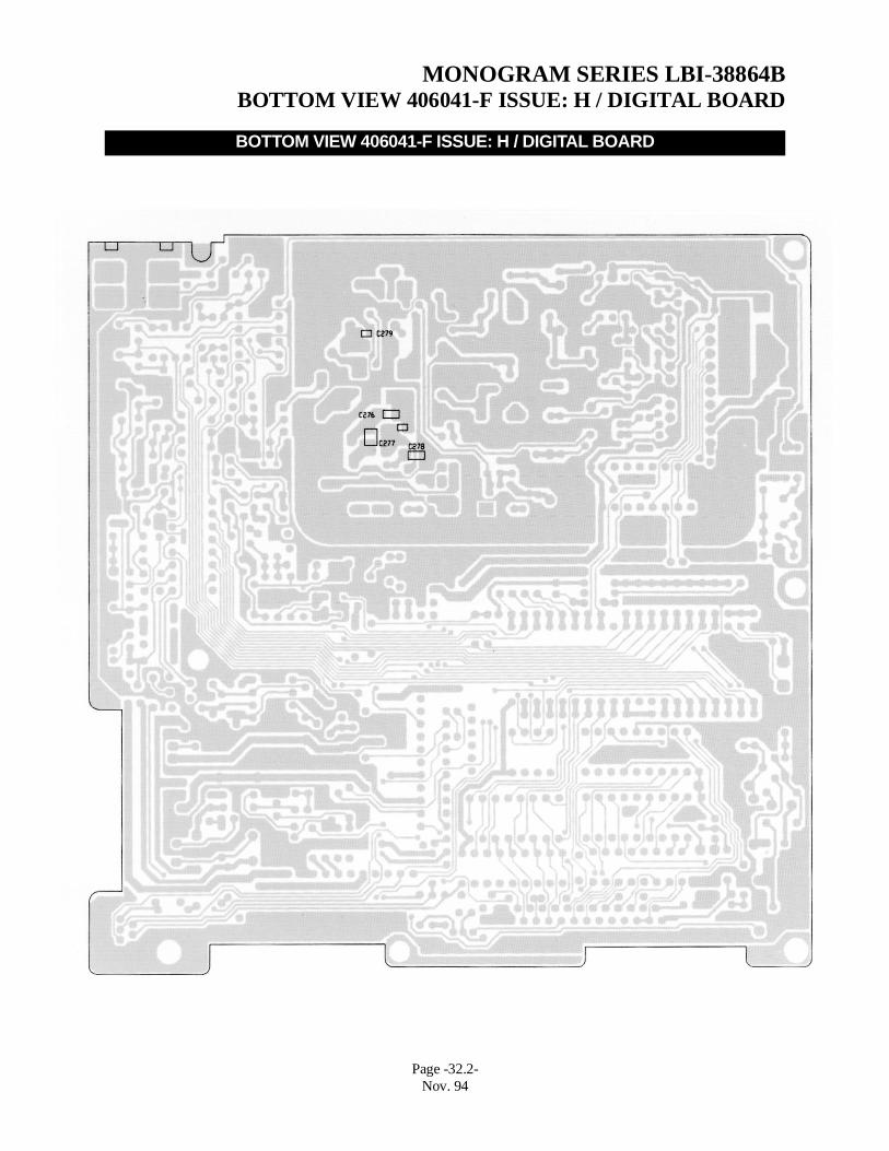
BOTTOM VIEW 406041-F ISSUE: H / DIGITAL BOARD
MONOGRAM SERIES LBI-38864BBOTTOM VIEW 406041-F ISSUE: H / DIGITAL BOARD
Page -32.2-Nov. 94
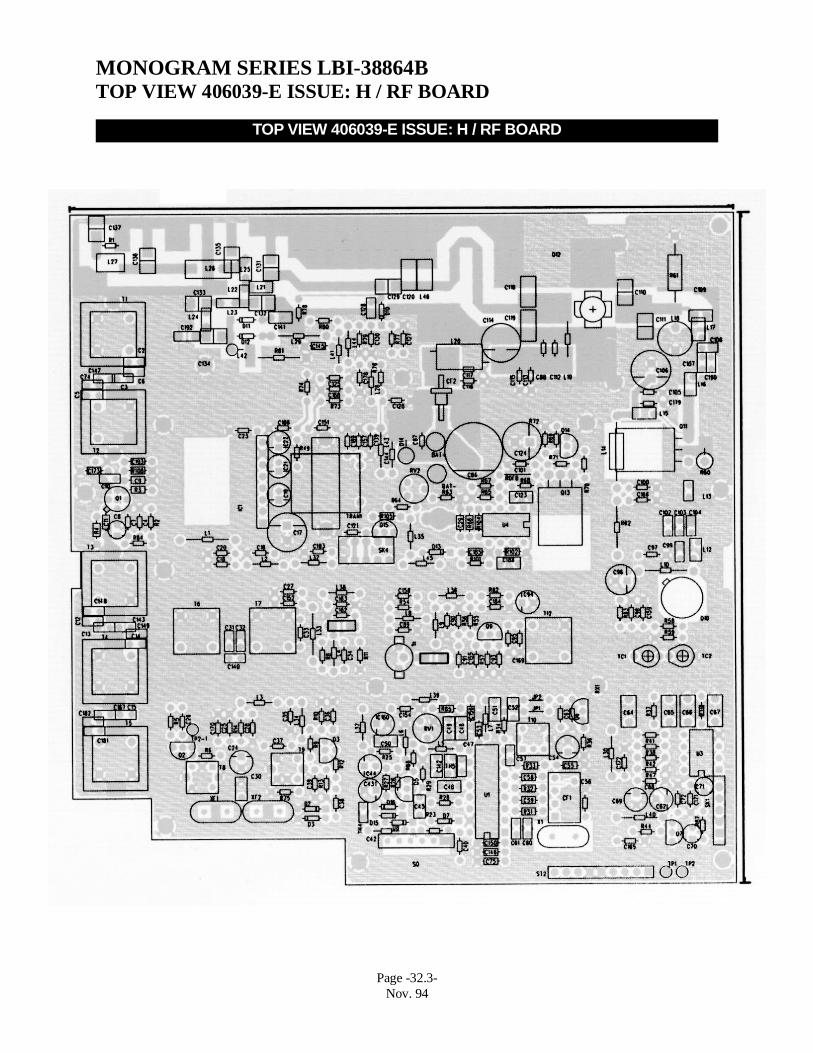
TOP VIEW 406039-E ISSUE: H / RF BOARD
MONOGRAM SERIES LBI-38864BTOP VIEW 406039-E ISSUE: H / RF BOARD
Page -32.3-Nov. 94
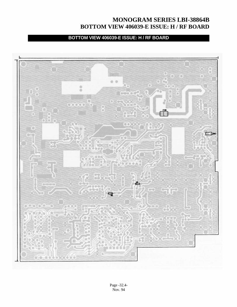
BOTTOM VIEW 406039-E ISSUE: H / RF BOARD
MONOGRAM SERIES LBI-38864BBOTTOM VIEW 406039-E ISSUE: H / RF BOARD
Page -32.4-Nov. 94

PRINTED CIRCUIT BOARDS
DISPLAY BOARD BOTTOM VIEW
DISPLAY BOARD TOP VIEW
VOLUME BOARD BOTTOM VIEWVOLUME BOARD TOP VIEW
MONOGRAM SERIES LBI-38864BPRINTED CIRCUIT BOARDS
Page -32.5-Nov. 94

PRINTED CIRCUIT BOARDS
406-968-C (RF. PCB) TOP 406-968-C (RF. PCB) BOTTOM
406-973-A TOP 406-973-A BOTTOM
406-969-F (DIG. PCB) TOP 406-969-F (DIG. PCB) BOTTOM
MONOGRAM SERIES LBI-38864BPRINTED CIRCUIT BOARDS
Page -32.6-Nov. 94

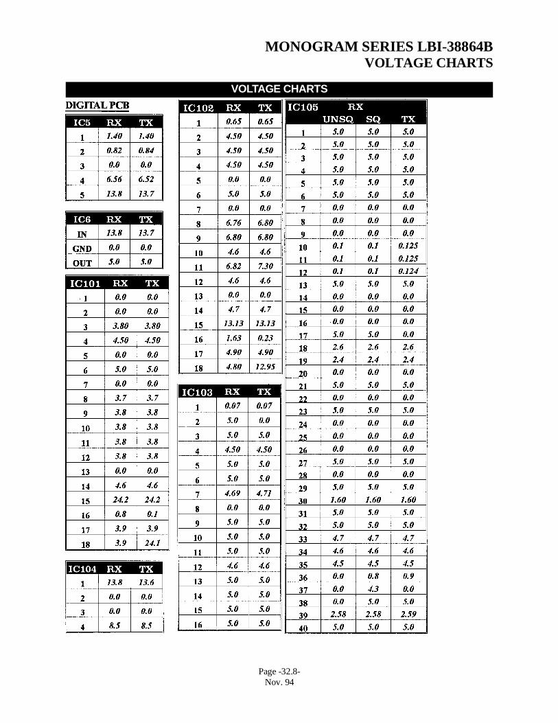
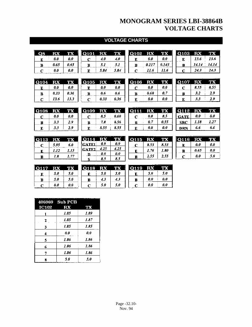
VOLTAGE CHARTS
MONOGRAM SERIES LBI-38864BVOLTAGE CHARTS
Page -32.7-Nov. 94
VOLTAGE CHARTS
MONOGRAM SERIES LBI-38864BVOLTAGE CHARTS
Page -32.8-Nov. 94

VOLTAGE CHARTS
MONOGRAM SERIES LBI-38864BVOLTAGE CHARTS
Page -32.9-Nov. 94
VOLTAGE CHARTS
MONOGRAM SERIES LBI-38864BVOLTAGE CHARTS
Page -32.10-Nov. 94

EXPLODED VIEWAND
EXPLODED VIEW PARTS LIST
Only those items indicated by shading will be stocked by After MarketServices. All other items are for reference only.
When ordering parts for your Monogram Series radio, precede all partnumbers with the prefix "R29/"
NOTE
Page - 33.0 -Oct. 94
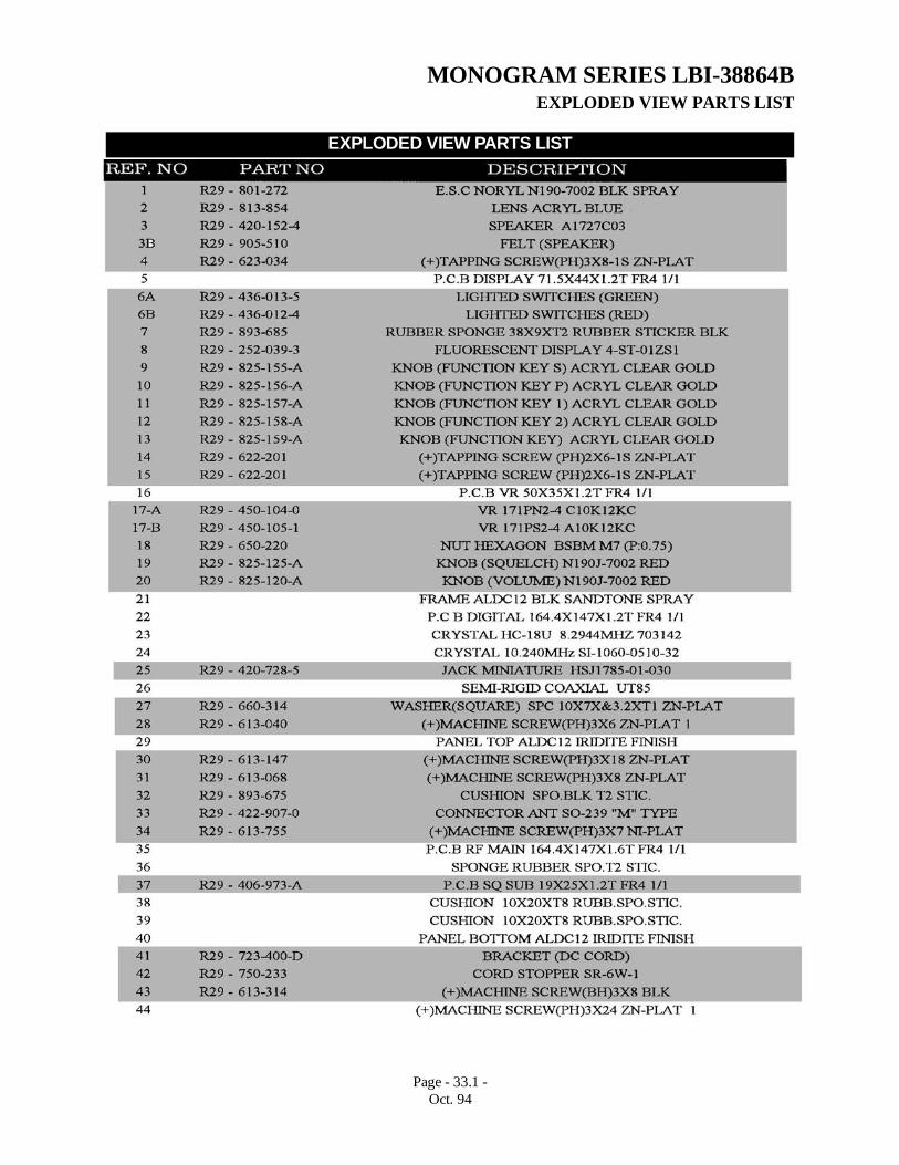
EXPLODED VIEW PARTS LIST
MONOGRAM SERIES LBI-38864BEXPLODED VIEW PARTS LIST
Page - 33.1 -Oct. 94

EXPLODED VIEW PARTS LIST
MONOGRAM SERIES LBI-38864BEXPLODED VIEW PARTS LIST
Page - 33.2 -Oct. 94

MGM-148 / MGM-160 EXPLODED VIEW
MONOGRAM SERIES LBI-38864BMGM-148 / MGM-160 EXPLODED VIEW
Page - 33.3 -Oct. 94

SCHEMATICS
Ericsson Inc.Private Radio SystemsMountain View RoadLynchburg,Virginia 245021-800-528-7711 (Outside USA, 804-528-7711) Printed in U.S.A.
Page -34-Nov. 94

RF BOARDR29/406039-E
LBI-38864B
34.1

DIGITAL BOARDR29/406041-F
LBI-38864B
34.2