layout, fabrication, and elementary logic design
TRANSCRIPT

Introduction to
CMOS VLSI
Design
Layout, Fabrication, and
Elementary Logic Design

CMOS VLSI DesignFabrication and Layout Slide 2
CMOS Fabrication
CMOS transistors
are fabricated on
silicon wafer
Lithography process
similar to printing
press
On each step,
different materials
are deposited or
etched

CMOS VLSI DesignFabrication and Layout Slide 3
Inverter Cross-section
Typically use p-type substrate for nMOS transistor
– Requires n-well for body of pMOS transistors
– Several alternatives: SOI, twin-tub, etc.
n+
p substrate
p+
n well
A
YGND V
DD
n+ p+
SiO2
n+ diffusion
p+ diffusion
polysilicon
metal1
nMOS transistor pMOS transistor

CMOS VLSI Design0: Introduction Slide 4
Well and Substrate Taps
Substrate must be tied to GND and n-well to VDD
Metal to lightly-doped semiconductor forms poor
connection called Shottky Diode
Use heavily doped well and substrate contacts / taps
n+
p substrate
p+
n well
A
YGND V
DD
n+p+
substrate tap well tap
n+ p+

CMOS VLSI DesignFabrication and Layout Slide 5
Inverter Mask Set
Transistors and wires are defined by masks
Cross-section taken along dashed line

CMOS VLSI DesignFabrication and Layout Slide 6
Fabrication Steps
Start with blank wafer
Build inverter from the bottom up
First step will be to form the n-well
– Cover wafer with protective layer of SiO2 (oxide)
– Remove layer where n-well should be built
– Implant or diffuse n dopants into exposed wafer
– Strip off SiO2
p substrate

CMOS VLSI DesignFabrication and Layout Slide 7
Oxidation
Grow SiO2 on top of Si wafer
– 900 – 1200 C with H2O or O2 in oxidation furnace
p substrate
SiO2

CMOS VLSI DesignFabrication and Layout Slide 8
Photoresist
Spin on photoresist
– Photoresist is a light-sensitive organic polymer
– Softens where exposed to light
p substrate
SiO2
Photoresist
CMOS VLSI DesignFabrication and Layout Slide 9
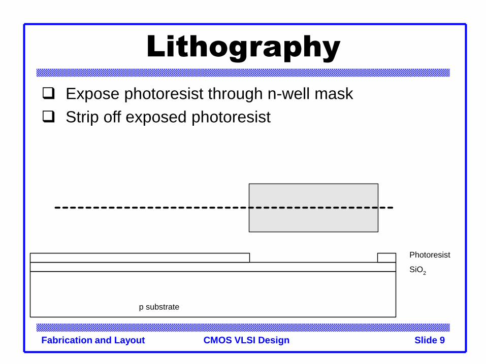
Lithography
Expose photoresist through n-well mask
Strip off exposed photoresist
p substrate
SiO2
Photoresist

CMOS VLSI DesignFabrication and Layout Slide 10
Etch
Etch oxide with hydrofluoric acid (HF)
– Seeps through skin and eats bone; nasty stuff!!!
Only attacks oxide where resist has been exposed
p substrate
SiO2
Photoresist
CMOS VLSI DesignFabrication and Layout Slide 11
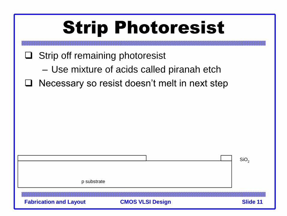
Strip Photoresist
Strip off remaining photoresist
– Use mixture of acids called piranah etch
Necessary so resist doesn’t melt in next step
p substrate
SiO2

CMOS VLSI DesignFabrication and Layout Slide 12
n-well
n-well is formed with diffusion or ion implantation
Diffusion
– Place wafer in furnace with arsenic gas
– Heat until As atoms diffuse into exposed Si
Ion Implanatation
– Blast wafer with beam of As ions
– Ions blocked by SiO2, only enter exposed Si
n well
SiO2

CMOS VLSI DesignFabrication and Layout Slide 13
Strip Oxide
Strip off the remaining oxide using HF
Back to bare wafer with n-well
Subsequent steps involve similar series of steps
p substrate
n well

CMOS VLSI DesignFabrication and Layout Slide 14
Polysilicon
Deposit very thin layer of gate oxide
– < 20 Å (6-7 atomic layers)
Chemical Vapor Deposition (CVD) of silicon layer
– Place wafer in furnace with Silane gas (SiH4)
– Forms many small crystals called polysilicon
– Heavily doped to be good conductor
Thin gate oxide
Polysilicon
p substraten well

CMOS VLSI DesignFabrication and Layout Slide 15
Polysilicon Patterning
Use same lithography process to pattern polysilicon
Polysilicon
p substrate
Thin gate oxide
Polysilicon
n well

CMOS VLSI DesignFabrication and Layout Slide 16
Self-Aligned Process
Use oxide and masking to expose where n+ dopants
should be diffused or implanted
N-diffusion forms nMOS source, drain, and n-well
contact
p substraten well

CMOS VLSI DesignFabrication and Layout Slide 17
N-diffusion
Pattern oxide and form n+ regions
Self-aligned process where gate blocks diffusion
Polysilicon is better than metal for self-aligned gates
because it doesn’t melt during later processing
p substraten well
n+ Diffusion

CMOS VLSI DesignFabrication and Layout Slide 18
N-diffusion
Historically dopants were diffused
Usually ion implantation today
But regions are still called diffusion
n wellp substrate
n+n+ n+

CMOS VLSI DesignFabrication and Layout Slide 19
N-diffusion
Strip off oxide to complete patterning step
n wellp substrate
n+n+ n+

CMOS VLSI DesignFabrication and Layout Slide 20
P-Diffusion
Similar set of steps form p+ diffusion regions for
pMOS source and drain and substrate contact
p+ Diffusion
p substraten well
n+n+ n+p+p+p+

CMOS VLSI DesignFabrication and Layout Slide 21
Contacts
Now we need to wire together the devices
Cover chip with thick field oxide
Etch oxide where contact cuts are needed
p substrate
Thick field oxide
n well
n+n+ n+p+p+p+
Contact

CMOS VLSI DesignFabrication and Layout Slide 22
Metallization
Sputter on aluminum over whole wafer
Pattern to remove excess metal, leaving wires
p substrate
Metal
Thick field oxide
n well
n+n+ n+p+p+p+
Metal

CMOS VLSI DesignFabrication and Layout Slide 23
How transistor looks like

CMOS VLSI DesignFabrication and Layout Slide 24
Silicon oxide interface

CMOS VLSI DesignFabrication and Layout Slide 25
A Modern CMOS Process

CMOS VLSI DesignFabrication and Layout Slide 26
Advanced metalization

CMOS VLSI DesignFabrication and Layout Slide 27
Advanced metalization
CMOS VLSI DesignFabrication and Layout Slide 28
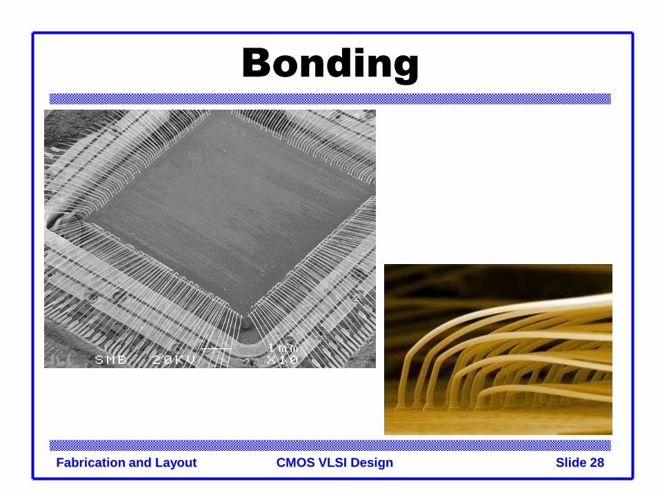
Bonding

CMOS VLSI DesignFabrication and Layout Slide 29
Design rules
CMOS VLSI DesignFabrication and Layout Slide 30
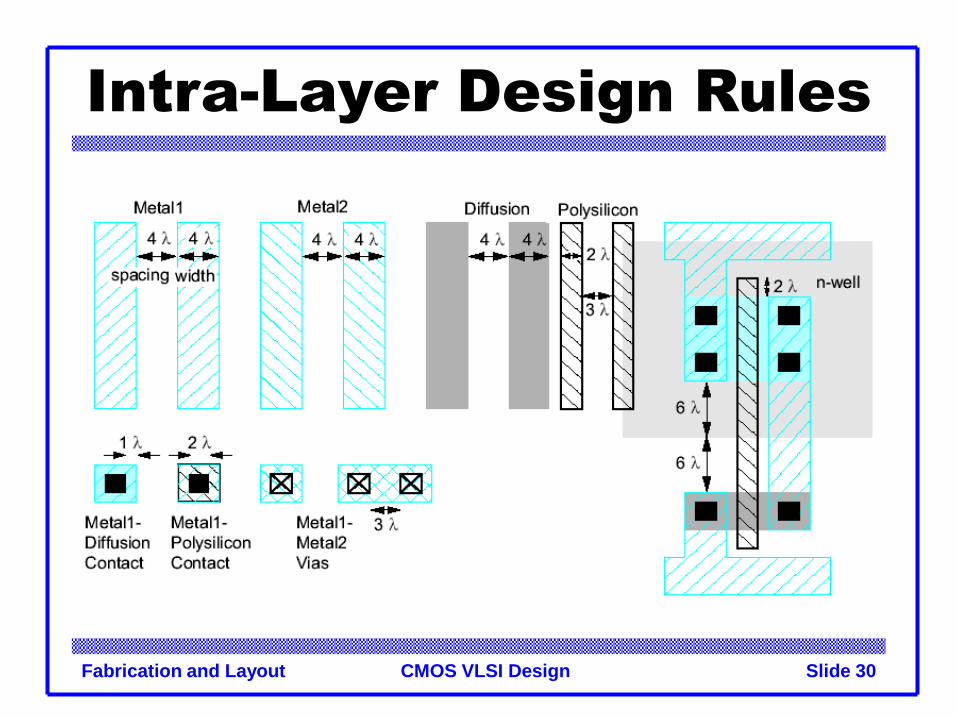
Intra-Layer Design Rules

CMOS VLSI DesignFabrication and Layout Slide 31
Transistor layout

CMOS VLSI DesignFabrication and Layout Slide 32
Vias and contacts
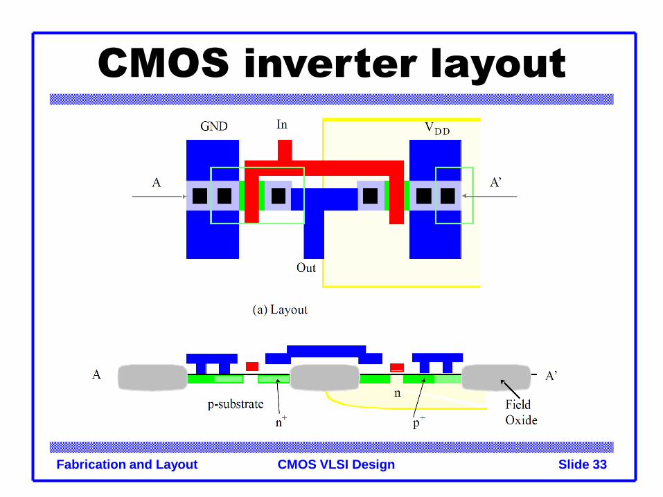
CMOS VLSI DesignFabrication and Layout Slide 33
CMOS inverter layout