laser triggered z-pinch broadband extreme ultraviolet source for
TRANSCRIPT
Laser triggered Z-pinch broadband extreme ultraviolet source for metrologyI. Tobin, L. Juschkin, Y. Sidelnikov, F. O’Reilly, P. Sheridan et al. Citation: Appl. Phys. Lett. 102, 203504 (2013); doi: 10.1063/1.4807172 View online: http://dx.doi.org/10.1063/1.4807172 View Table of Contents: http://apl.aip.org/resource/1/APPLAB/v102/i20 Published by the American Institute of Physics. Additional information on Appl. Phys. Lett.Journal Homepage: http://apl.aip.org/ Journal Information: http://apl.aip.org/about/about_the_journal Top downloads: http://apl.aip.org/features/most_downloaded Information for Authors: http://apl.aip.org/authors

Laser triggered Z-pinch broadband extreme ultraviolet source for metrology
I. Tobin,1 L. Juschkin,2,3 Y. Sidelnikov,4 F. O’Reilly,2 P. Sheridan,5 E. Sokell,2
and J. G. Lunney1,a)
1School of Physics, Trinity College Dublin, Dublin 2, Ireland2School of Physics, University College Dublin, Belfield, Dublin 4, Ireland3Department of Physics, RWTH Aachen University, Steinbachstr. 15 D-52074 Aachen, Germany4ISAN Institute of Spectroscopy, Fizicheskaya Str. 5, Troitsk, Moscow Region 142190, Russia5Newlambda Technologies, UCD Science Centre North, Belfield, Dublin 4, Ireland
(Received 20 December 2012; accepted 4 May 2013; published online 21 May 2013)
We compare the extreme ultraviolet emission characteristics of tin and galinstan (atomic %:
Ga: 78.35, In: 14.93, Sn: 6.72) between 10 nm and 18 nm in a laser-triggered discharge between
liquid metal-coated electrodes. Over this wavelength range, the energy conversion efficiency for
galinstan is approximately half that of tin, but the spectrum is less strongly peaked in the 13–15 nm
region. The extreme ultraviolet source dimensions were 110 6 25 lm diameter and 500 6 125 lm
length. The flatter spectrum, and �19 �C melting point, makes this galinstan discharge a relatively
simple high radiance extreme ultraviolet light source for metrology and scientific applications.VC 2013 AIP Publishing LLC. [http://dx.doi.org/10.1063/1.4807172]
Laser produced plasmas (LPPs) and discharge produced
plasmas (DPPs) have been extensively studied as radiation
sources for extreme ultraviolet (EUV) lithography at
13.5 nm.1 Current state-of-the-art sources use tin as the emit-
ter material because it has strong emission at 13.5 nm due to
4 p–4 d and 4 d–4f unresolved transition arrays (UTAs) in Sn
XI–XIV.2 Discharge sources have the potential to provide
higher wall-plug efficiency than LPPs.3 EUV emission from
a Z-pinch in a laser-triggered discharge between rotating
electrodes coated with liquid tin has been studied previ-
ously.4,5 The liquid metal coating overcomes the problem of
electrode erosion, but it is necessary to maintain the tin
above its melting temperature of 232 �C. The EUV emission
spectrum of pure tin plasma, at the appropriate conditions, is
relatively narrow-band, with �50% of emission in the
13–15 nm range. For EUV metrology, the source parameters
of interest are spectral radiance, wavelength range, and emis-
sion uniformity, as well as cost and ease of operation.
Compared to pure tin, galinstan (at. %: Ga: 78.35, In: 14.93,
Sn: 6.72) has spectrally flat broadband emission in the
10–18 nm range arising from each of its transition-rich con-
stituents. This makes galinstan a useful source for reflectr-
ometry, where the reflectivity of EUV mirrors needs to be
measured over an extended wavelength range for the detec-
tion of reflectance inhomogeneities. Being liquid at room
temperature makes a galinstan-based source somewhat sim-
pler in construction and operation than those using higher
melting point materials. Like tin, galinstan can also be uti-
lized as a mirror coating in collector optics,6 thus avoiding
damage of the EUV collector by plasma deposition or ion
sputtering. This paper describes the results of an experiment
to characterise the EUV emission of laser-triggered Z-pinch
discharges in galinstan, which has not been studied before in
this type of source. The spatial and spectral characteristics of
the EUV emission, along with ion outflow, are investigated
for different discharge energies. Comparison is made with
laser triggered discharges in tin which are similar to the
state-of-the-art sources for 13.5 nm lithography.
The Z-pinch EUV source is based on a laser-triggered
discharge struck between two rotating disc electrodes, which
are coated in liquid metal by partial immersion in liquid
metal baths. The source was developed at the Russian
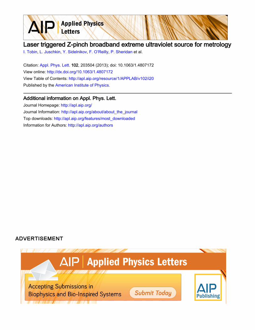
Institute of Spectroscopy (ISAN).5 Figure 1 shows plan and
side views of the electrode geometry and the arrangement of
the diagnostic instruments. The disc electrodes are tilted so
that the separation at closest approach is 4 mm. For galinstan,
the metal baths are not heated, while for tin they are heated
to 300 �C. The anode is grounded to the chamber while the
cathode is connected to the live electrode of a 0.39 lF capac-
itor bank. The charging voltage was varied from 2.5 to
5.5 kV (1.25 to 6.05 J).
The discharge is triggered using a 1064 nm, 30 ns laser
pulse to form a LPP on the cathode electrode at the point of
closest approach to the anode. The laser is focused to a
400 lm diameter spot and the energy was varied in the range
of 5–80 mJ by means of a rotatable half-wave plate and
polarizing beam splitter. The laser operates at a maximum
repetition rate of 2 Hz or in single pulse mode. The LPP
expands away from the cathode and triggers the discharge
when it reaches the anode. The derivative of the discharge
current is recorded using a Rogowski coil placed in the vicin-
ity of the current path between the capacitor and the cathode.
A 0.057 cm2 aperture Faraday cup ion detector, placed
in the horizontal plane at a distance of 50 cm from the dis-
charge and at an angle of 60� from the discharge axis (facing
cathode), was used to monitor the plasma outflow from the
discharge. The cup collector was biased at �12 V to reject
plasma electrons and was equipped with a 65 mT transverse
magnetic field to suppress the detection of ion-induced sec-
ondary electron emission and photo-electron emission due to
vacuum ultraviolet and EUV emission from the plasma.
From the ion time-of-flight (TOF) measurements recorded
with the cup, it is possible to estimate the ion energy distri-
bution and ion flux at the position of the cup. These values
are of interest for assessing the level of ion sputtering of any
a)Author to whom correspondence should be addressed. Electronic mail:
0003-6951/2013/102(20)/203504/4/$30.00 VC 2013 AIP Publishing LLC102, 203504-1
APPLIED PHYSICS LETTERS 102, 203504 (2013)
optical element placed near the discharge, or for the design
of systems to mitigate such sputtering.
Several devices were used to measure the EUV emis-
sion. The time-integrated emission spectrum was measured
in the 10–18 nm range using an absolutely calibrated grazing
incidence Jenoptik spectrometer equipped with a back illu-
minated silicon CCD detector7,8 viewing the plasma in the
horizontal plane at 60� from the discharge axis facing the an-
ode. The spectral resolution of the spectrometer is �0.03 nm.
The absolute emission in a 2% bandwidth at 13.5 nm was
measured with a PhysTeX EUV detector comprised of a
calibrated EUV sensitive photodiode9,10 combined with two
Mo/Si multilayer mirrors and a 250 nm thick Zr filter. The
PhysTeX EUV detector viewed the plasma at 60� above the
horizontal plane but normal to the discharge axis. Thus, it
was possible to make two independent measurements of the
EUV emission at different angles with respect to the dis-
charge axis. The spatial distribution of the EUV source was
recorded by using a 125 mm radius spherical Mo/Si multi-
layer mirror at near normal incidence to form a 13� magni-
fied image on a CCD, as shown in Fig.1. The imaging
system had a resolution of �5 lm and included a 1 lm Zr
filter to provide spectral filtering in the 10–18 nm region.
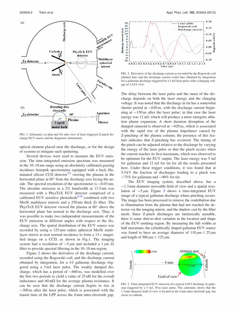
Figure 2 shows the derivative of the discharge current,
recorded using the Rogowski coil, and the discharge current
obtained by integration, for a 4 J galinstan discharge trig-
gered using a 5 mJ laser pulse. The weakly damped dis-
charge, which has a period of �660 ns, was modelled over
the first two periods to yield a value of 25 nH for the overall
inductance and 60 mX for the average plasma resistance. It
can be seen that the discharge current begins to rise at
�300 ns after the laser pulse, which is associated with the
transit time of the LPP across the 4 mm inter-electrode gap.
The delay between the laser pulse and the onset of the dis-
charge depends on both the laser energy and the charging
voltage. It was noted that the discharge in tin has a somewhat
shorter period at �620 ns, with the discharge current begin-
ning at �150 ns after the laser pulse; in that case the laser
energy was 12 mJ, which will produce a more energetic abla-
tion plume expansion. A short duration disruption of the
damped sinusoid is observed at �420 ns, which is associated
with the rapid rise of the plasma impedance caused by
Z-pinching of the plasma column; the presence of this fea-
ture indicates that Z-pinching has occurred. The timing of
the pinch can be adjusted relative to the discharge by varying
the energy of the laser pulse so that the pinch occurs when
the current reaches its first maximum, which was observed to
be optimum for the EUV output. The laser energy was 5 mJ
for galinstan and 12 mJ for tin for all the results presented
here. Under these trigger conditions, it was found that at
5.5 kV the fraction of discharges leading to a pinch was
�75% for galinstan and �90% for tin.
The EUV imaging system, described above, has a
�1.3 mm diameter moveable field of view and a spatial reso-
lution of �5 lm. Figure 3 shows a time-integrated EUV
image of a typical galinstan discharge where pinching occurs.
The image has been processed to remove the contribution due
to illumination from the plasma that had not reached the de-
tector via the imaging mirror, and the shadow cast by the filter
mesh. Since Z-pinch discharges are intrinsically unstable,
there is some shot-to-shot variation in the location and shape
of the EUV emitting region. By measuring the full widths at
half maximum, the cylindrically shaped galinstan EUV source
was found to have an average diameter of 110 lm 6 25 lm
and length of 500 lm 6 125 lm.
FIG. 1. Schematic (a) plan and (b) side-view of laser triggered Z-pinch dis-
charge EUV source and the diagnostic instruments.
FIG. 2. Derivative of the discharge current as recorded by the Rogowski coil
(dashed line) and the discharge current (solid line) obtained by integration
for a galinstan discharge triggered by a 5 mJ laser pulse with a charging volt-
age of 4.5 kV (4 J).
FIG. 3. Time-integrated EUV emission of a typical 4.05 J discharge in galin-
stan triggered by a 5 mJ, 30 ns laser pulse. The schematic shows that the
1.3 mm diameter field of view is located in the 4 mm inter-electrode gap, but
closer to cathode.
203504-2 Tobin et al. Appl. Phys. Lett. 102, 203504 (2013)
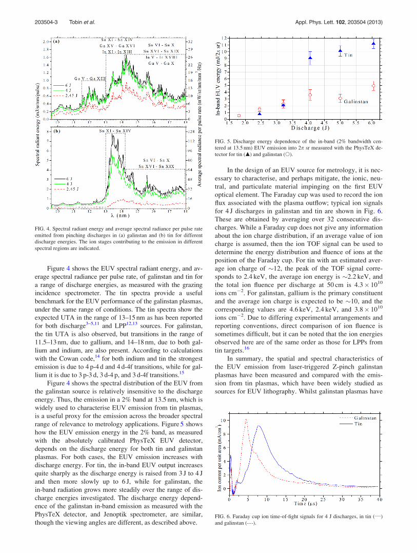
Figure 4 shows the EUV spectral radiant energy, and av-
erage spectral radiance per pulse rate, of galinstan and tin for
a range of discharge energies, as measured with the grazing
incidence spectrometer. The tin spectra provide a useful
benchmark for the EUV performance of the galinstan plasmas,
under the same range of conditions. The tin spectra show the
expected UTA in the range of 13–15 nm as has been reported
for both discharge3–5,11 and LPP12,13 sources. For galinstan,
the tin UTA is also observed, but transitions in the range of
11.5–13 nm, due to gallium, and 14–18 nm, due to both gal-
lium and indium, are also present. According to calculations
with the Cowan code,14 for both indium and tin the strongest
emission is due to 4 p-4 d and 4 d-4f transitions, while for gal-
lium it is due to 3 p-3 d, 3 d-4 p, and 3 d-4f transitions.15
Figure 4 shows the spectral distribution of the EUV from
the galinstan source is relatively insensitive to the discharge
energy. Thus, the emission in a 2% band at 13.5 nm, which is
widely used to characterise EUV emission from tin plasmas,
is a useful proxy for the emission across the broader spectral
range of relevance to metrology applications. Figure 5 shows
how the EUV emission energy in the 2% band, as measured
with the absolutely calibrated PhysTeX EUV detector,
depends on the discharge energy for both tin and galinstan
plasmas. For both cases, the EUV emission increases with
discharge energy. For tin, the in-band EUV output increases
quite sharply as the discharge energy is raised from 3 J to 4 J
and then more slowly up to 6 J, while for galinstan, the
in-band radiation grows more steadily over the range of dis-
charge energies investigated. The discharge energy depend-
ence of the galinstan in-band emission as measured with the
PhysTeX detector, and Jenoptik spectrometer, are similar,
though the viewing angles are different, as described above.
In the design of an EUV source for metrology, it is nec-
essary to characterise, and perhaps mitigate, the ionic, neu-
tral, and particulate material impinging on the first EUV
optical element. The Faraday cup was used to record the ion
flux associated with the plasma outflow; typical ion signals
for 4 J discharges in galinstan and tin are shown in Fig. 6.
These are obtained by averaging over 32 consecutive dis-
charges. While a Faraday cup does not give any information
about the ion charge distribution, if an average value of ion
charge is assumed, then the ion TOF signal can be used to
determine the energy distribution and fluence of ions at the
position of the Faraday cup. For tin with an estimated aver-
age ion charge of �12, the peak of the TOF signal corre-
sponds to 2.4 keV, the average ion energy is �2.2 keV, and
the total ion fluence per discharge at 50 cm is 4.3� 1010
ions cm�2. For galinstan, gallium is the primary constituent
and the average ion charge is expected to be �10, and the
corresponding values are 4.6 keV, 2.4 keV, and 3.8� 1010
ions cm�2. Due to differing experimental arrangements and
reporting conventions, direct comparison of ion fluence is
sometimes difficult, but it can be noted that the ion energies
observed here are of the same order as those for LPPs from
tin targets.16
In summary, the spatial and spectral characteristics of
the EUV emission from laser-triggered Z-pinch galinstan
plasmas have been measured and compared with the emis-
sion from tin plasmas, which have been widely studied as
sources for EUV lithography. Whilst galinstan plasmas have
FIG. 4. Spectral radiant energy and average spectral radiance per pulse rate
emitted from pinching discharges in (a) galinstan and (b) tin for different
discharge energies. The ion stages contributing to the emission in different
spectral regions are indicated.
FIG. 5. Discharge energy dependence of the in-band (2% bandwidth cen-
tered at 13.5 nm) EUV emission into 2p sr measured with the PhysTeX de-
tector for tin (�) and galinstan (�).
FIG. 6. Faraday cup ion time-of-fight signals for 4 J discharges, in tin (___)
and galinstan (---).
203504-3 Tobin et al. Appl. Phys. Lett. 102, 203504 (2013)

lower in-band conversion efficiencies than tin plasmas, the
EUV emission from galinstan has a broader, less sharply
peaked spectral profile, due to the emission from the indium
and gallium constituents. Thus, a galinstan source is more
suited to EUV metrology applications like reflectrometry of
EUV optics and mask blanks. Furthermore, the use of galin-
stan allows continuously rotating liquid-metal coated elec-
trodes, which are required for high repetition rate, to be
provided at room temperature, which simplifies the design
and operation of small laboratory, or metrology, EUV sour-
ces. For both galinstan and tin, the EUV output increases
strongly when the plasma is Z-pinched. Pinching occurs
most readily when the energy in the laser ablation pulse is
adjusted so that the pinch occurs at the time of the first maxi-
mum of the discharge current. Future studies to optimise the
stability and reproducibility of the EUV emission from laser-
triggered Z-pinch galinstan-based plasmas will pave the way
for development of laboratory-based metrology sources that
may be used over a range of EUV wavelengths.
This publication resulted from research conducted with
the financial support of Science Foundation Ireland under
grant “SFI 07/IN.1/I1771,” by Enterprise Ireland under
grants “TD20090346” and “PC/07/069” and co-funded by
the European Regional Development fund. This research
was supported by the technical staff in the mechanical and
electronics workshops in University College Dublin. The
authors also acknowledge Imam Kambali for the theoretical
calculations of gallium, indium, and tin transitions using
Cowan code.
1V. Bakshi, EUV Lithography (SPIE Press, Bellingham, WA, 2006).2G. O’Sullivan and R. Faulkner, Opt. Eng. 33(12), 3978 (1994).3G. Schriever, O. Semprez, J. Jonkers, M. Yoshioka, and R. Apetz,
J. Micro/Nanolith. MEMS MOEMS 11(2), 021104 (2012).4K. Gielissen, Y. Sidelnikov, D. Glushkov, W. A. Soer, V. Banine, and
J. J. A. M. V. D. Mullen, J. Appl. Phys. 107, 013301 (2010).5V. Y. Banine, K. N. Koshelev, and G. H. P. M. Swinkels, J. Phys. D 44,
253001 (2011).6K. Fahy, F. O’Reilly, E. Scally, and P. Sheridan, Proc. SPIE 7802, 78020K
(2010).7M. C. Schuermann, T. Missalla, K. R. Mann, S. Kranzusch, R. M. Klein, F.
Scholze, G. Ulm, R. Lebert, and L. Juschkin, Proc. SPIE 5037, 378 (2003).8T. Missalla, M. C. Schuermann, R. Lebert, C. Wies, L. Juschkin, Roman
M. Klein, F. Scholze, G. Ulm, A. Egbert, B. Tkachenko, and B. N.
Chichkov, Proc. SPIE 5374, 979 (2004).9L. A. Shmaenok, in International SEMATECH EUV Source Workshop
Meeting, February 2004.10P. Dunne, O. Morris, E. Sokell, F. O’Reilly, G. O’Sullivan, N. Murphy, P.
Hayden, and V. Bakshi, SEMATECH Document ID No. 06114813A-ENG
(2006).11M. Yoshioka, Y. Teramoto, J. Jonkers, M. C. Sch€urmann, R. Apetz, V.
Kilian, and M. Corthout, Proc. SPIE 7969, 79691G (2011).12P. Hayden, A. Cummings, N. Murphy, G. O’Sullivan, P. Sheridan, J.
White, and P. Dunne, J. Appl. Phys. 99, 093302 (2006).13J. White, P. Dunne, P. Hayden, F. O’Reilly, and G. O’Sullivan, Appl.
Phys. Lett. 90, 181502 (2007).14R. D. Cowan, Theory of Atomic Structure and Spectra (University of
California Press, Berkeley, CA, 1981).15I. Kambali, private communication (2012).16R. W. Coons, S. S. Harilal, D. Campos, and A. Hassanein, J. Appl. Phys.
108, 063306 (2010).
203504-4 Tobin et al. Appl. Phys. Lett. 102, 203504 (2013)