large-scale and facial fabrication of pbs nanorods by ... · large-scale and facial fabrication of...
TRANSCRIPT
Contents lists available at ScienceDirect
Materials Science in Semiconductor Processing
Materials Science in Semiconductor Processing 21 (2014) 98–103
1369-80http://d
n CorrE-m
journal homepage: www.elsevier.com/locate/mssp
Large-scale and facial fabrication of PbS nanorodsby sulfuration of a Pb sheet
Mohsen Cheraghizade a, Ramin Yousefi b,n, Farid Jamali-Sheini c,Abdolhossein Saáedi a, Nay Ming Huang d
a Department of Electrical Engineering, Bushehr Branch, Islamic Azad University (I.A.U), Bushehr, Iranb Department of Physics, Masjed-Soleiman Branch, Islamic Azad University (I.A.U), Masjed-Soleiman, Iranc Department of Physics, Ahwaz Branch, Islamic Azad University, Ahwaz, Irand Low Dimensional Materials Research Center, Department of Physics, Faculty of Science, University of Malaya,50603 Kuala Lumpur, Malaysia
a r t i c l e i n f o
Keywords:PbS nanorodsSulfurationVapor depositionRamanOptical properties
01/$ - see front matter & 2014 Elsevier Ltd.x.doi.org/10.1016/j.mssp.2014.01.009
esponding author. Tel.: þ98 9166224993; faail address: [email protected] (R. Yo
a b s t r a c t
PbS nanostructures were synthesized by sulfuration of lead sheets in a tube furnace undersulfur ambiance. The lead sheets were placed in different temperature zones, between 330and 470 1C. Field emission scanning electron microscope (FESEM) images showed thatonly the lead sheet placed at 330 1C showed nanorods morphology. The preparednanorods exhibited a rectangular shape with an average diameter of 95 nm and anaverage length of 400 nm. The phase and composition of the product were identified byx-ray diffraction (XRD) pattern and x-ray photoelectron spectra (XPS). The patternindicated that these PbS nanorods were with a cubic phase and the XPS result showedbinding energy for lead and sulfur that belonged to PbS structure. In addition, Ramanmeasurements confirmed the XRD pattern and XPS results and indicated three Ramanactive modes, which belonged to PbS phase for the nanorods. The optical properties of theproducts were characterized by UV–visible and room temperature photoluminescence(PL) spectrometers. The optical characterization results showed a band gap for the PbSnanorods in the infrared region.
& 2014 Elsevier Ltd. All rights reserved.
1. Introduction
Metal chalcogenide semiconductors have attractedconsiderable attention because of their potential forseveral applications. In fact, semiconducting metal chalcogen-ide nanocrystals (II–VI and IV–VI) are a class of materials thatexhibit band gap energies spanning from the mid-to-nearinfrared (PbS, PbSe, PbTe) to the visible (CdS, CdSe, CdTe) andinto the ultraviolet (ZnS, ZnSe) regions [1–4].
Among these metal chalcogenides, lead sulfide (PbS) isone of the compound semiconductor with a narrow and
All rights reserved.
x: þ98 6813330093.usefi).
direct band gap around 0.41 eV at the room temperature.It has important optical applications such as solar cells,infrared detectors [5], solar control coatings [6], optical fibers,and broadband optical amplifiers [7]. In addition, PbS is anextremely promising material for a large number of applica-tions in the mid- and near-infrared emission and detectionrange, biological applications, and optoelectronic devicesowing to its wide range of size-dependent properties [8].So far, various forms of PbS nanostructures such as nano-wires [9], nanorods [10–12] and nanoclusters [13] werereported, which were grown by various methods such asthe polymeric method [14], chemical bath deposition (CBD)[15], electrochemical deposition [9], hydrothermal [16,17],and vacuum evaporation [18]. Most of these techniques areusually complex, expensive, and time consuming.

M. Cheraghizade et al. / Materials Science in Semiconductor Processing 21 (2014) 98–103 99
Based on these reasons, in this work we present asimple and cost effective method for growth of PbSnanorods on a large scale. In fact, we report and discussthe characterization of the PbS nanorods prepared by asimple sulfuration of a lead sheet in a CVD set-up for thefirst time. Morphological, structural, and optical properties
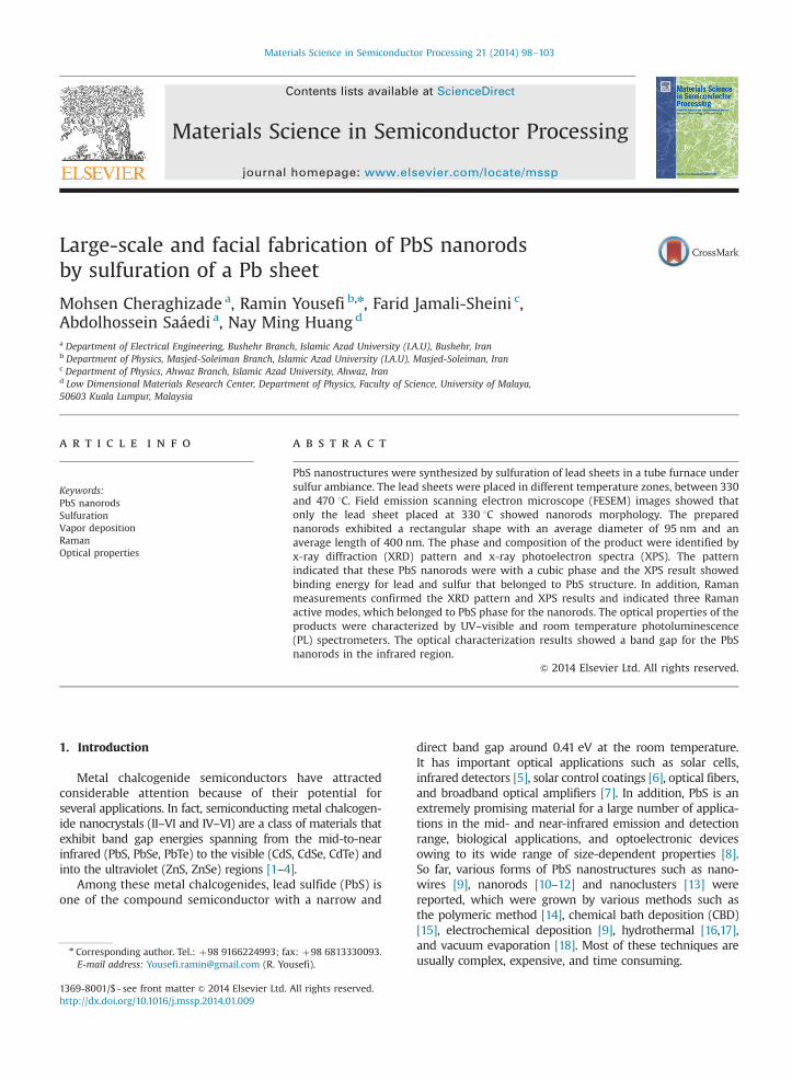
Fig. 1. (a) Schematic of the set-up that was used to grow PbS nanostructures.(b) A photograph of the lead sheet before and after sulfuration.
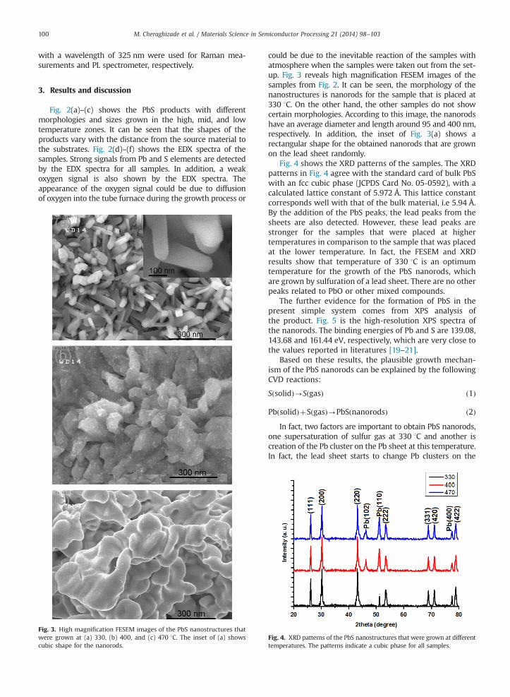
Fig. 2. FESEM images of the PbS nanostructures that were grown at (a) 330, (grown at (a) 330, (b) 400, and (c) 470 1C.
of these nanorods were studied by several tools and theresults were quite promising.
2. Experimental sections
The PbS nanostructures were grown by the followingprocedure. Three high purity Pb sheets (99.99%) with dimen-sions of �2�1 cm2 and a thickness of 0.5 mm were used assubstrates. The sheets were ultrasonically cleaned with acet-one and methanol for 10 min in each solvent. Then the sheetswere put into a horizontal tube furnace (CVD set-up) at 330,400 and 470 1C. Stoichiometric sulfur powder (Merck, sulfur(S8) (99.999%)) was used as the source material to create thesulfur ambiance in the tube furnace in an alumina boat at theright side of the furnace (at 185 1C) (Fig. 1(a)). High purity N2
gas was fed at about 120 sccm into the furnace at one end,while the other end was connected to a rotary pump. Thegrowth process was allowed to proceed for 1 h. Vacuum of50 Torr was maintained inside the tube furnace duringsulfuration of the Pb sheets. In this manner, the PbS nanos-tructures were formed on the Pb sheets (Fig. 1(b)).
The morphology and crystal structure of the productswere investigated using a field emission scanning electronmicroscope (FESEM, Hitachi S4160) and an x-ray diffract-ometer (XRD Seifert ID 3003). The elemental contents of theproducts were measured by using energy dispersive x-ray(EDX, Quanta 200 F) and x-ray photoelectron spectra (XPS)(VG-Microtech ESCA-2000 with Mg Kα radiation as theexcitation source). Room temperature photoluminescence(Jobin Yvon Horiba HR 800 UV), UV–vis (Lambda25-Perkin-Elmer) and Raman (Bruker-Senterra Raman Spec-trometer) spectrometers were employed to study the opticalproperties and crystallinity of the PbS nanostructures. A Nd:YLF laser with a wavelength of 785 nm and a He–Cd laser
b) 400, and (c) 470 1C. EDX spectrum of the PbS nanostructures that were
M. Cheraghizade et al. / Materials Science in Semiconductor Processing 21 (2014) 98–103100
with a wavelength of 325 nm were used for Raman mea-surements and PL spectrometer, respectively.
3. Results and discussion
Fig. 2(a)–(c) shows the PbS products with differentmorphologies and sizes grown in the high, mid, and lowtemperature zones. It can be seen that the shapes of theproducts vary with the distance from the source material tothe substrates. Fig. 2(d)–(f) shows the EDX spectra of thesamples. Strong signals from Pb and S elements are detectedby the EDX spectra for all samples. In addition, a weakoxygen signal is also shown by the EDX spectra. Theappearance of the oxygen signal could be due to diffusionof oxygen into the tube furnace during the growth process or
Fig. 3. High magnification FESEM images of the PbS nanostructures thatwere grown at (a) 330, (b) 400, and (c) 470 1C. The inset of (a) showscubic shape for the nanorods.
could be due to the inevitable reaction of the samples withatmosphere when the samples were taken out from the set-up. Fig. 3 reveals high magnification FESEM images of thesamples from Fig. 2. It can be seen, the morphology of thenanostructures is nanorods for the sample that is placed at330 1C. On the other hand, the other samples do not showcertain morphologies. According to this image, the nanorodshave an average diameter and length around 95 and 400 nm,respectively. In addition, the inset of Fig. 3(a) shows arectangular shape for the obtained nanorods that are grownon the lead sheet randomly.
Fig. 4 shows the XRD patterns of the samples. The XRDpatterns in Fig. 4 agree with the standard card of bulk PbSwith an fcc cubic phase (JCPDS Card No. 05-0592), with acalculated lattice constant of 5.972 Å. This lattice constantcorresponds well with that of the bulk material, i.e 5.94 Å.By the addition of the PbS peaks, the lead peaks from thesheets are also detected. However, these lead peaks arestronger for the samples that were placed at highertemperatures in comparison to the sample that was placedat the lower temperature. In fact, the FESEM and XRDresults show that temperature of 330 1C is an optimumtemperature for the growth of the PbS nanorods, whichare grown by sulfuration of a lead sheet. There are no otherpeaks related to PbO or other mixed compounds.
The further evidence for the formation of PbS in thepresent simple system comes from XPS analysis ofthe product. Fig. 5 is the high-resolution XPS spectra ofthe nanorods. The binding energies of Pb and S are 139.08,143.68 and 161.44 eV, respectively, which are very close tothe values reported in literatures [19–21].
Based on these results, the plausible growth mechan-ism of the PbS nanorods can be explained by the followingCVD reactions:
SðsolidÞ-SðgasÞ ð1Þ
PbðsolidÞþSðgasÞ-PbSðnanorodsÞ ð2ÞIn fact, two factors are important to obtain PbS nanorods,
one supersaturation of sulfur gas at 330 1C and another iscreation of the Pb cluster on the Pb sheet at this temperature.In fact, the lead sheet starts to change Pb clusters on the
Fig. 4. XRD patterns of the PbS nanostructures that were grown at differenttemperatures. The patterns indicate a cubic phase for all samples.
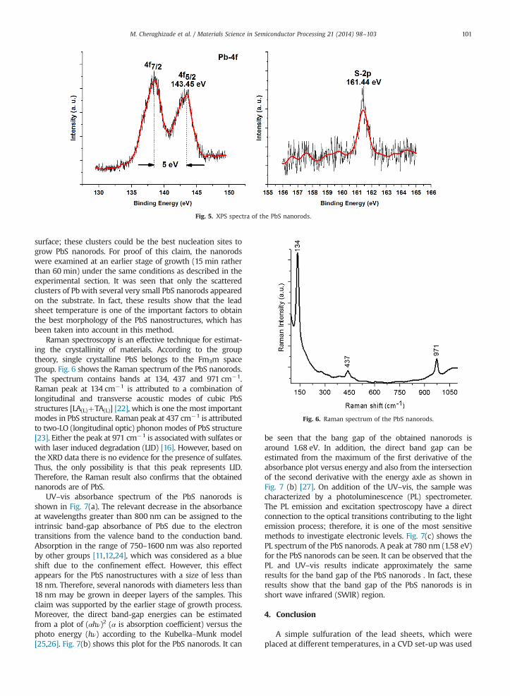
Fig. 5. XPS spectra of the PbS nanorods.
Fig. 6. Raman spectrum of the PbS nanorods.
M. Cheraghizade et al. / Materials Science in Semiconductor Processing 21 (2014) 98–103 101
surface; these clusters could be the best nucleation sites togrow PbS nanorods. For proof of this claim, the nanorodswere examined at an earlier stage of growth (15 min ratherthan 60 min) under the same conditions as described in theexperimental section. It was seen that only the scatteredclusters of Pb with several very small PbS nanorods appearedon the substrate. In fact, these results show that the leadsheet temperature is one of the important factors to obtainthe best morphology of the PbS nanostructures, which hasbeen taken into account in this method.
Raman spectroscopy is an effective technique for estimat-ing the crystallinity of materials. According to the grouptheory, single crystalline PbS belongs to the Fm3m spacegroup. Fig. 6 shows the Raman spectrum of the PbS nanorods.The spectrum contains bands at 134, 437 and 971 cm�1.Raman peak at 134 cm�1 is attributed to a combination oflongitudinal and transverse acoustic modes of cubic PbSstructures [LA(L)þTA(L)] [22], which is one the most importantmodes in PbS structure. Raman peak at 437 cm�1 is attributedto two-LO (longitudinal optic) phonon modes of PbS structure[23]. Either the peak at 971 cm�1 is associated with sulfates orwith laser induced degradation (LID) [16]. However, based onthe XRD data there is no evidence for the presence of sulfates.Thus, the only possibility is that this peak represents LID.Therefore, the Raman result also confirms that the obtainednanorods are of PbS.
UV–vis absorbance spectrum of the PbS nanorods isshown in Fig. 7(a). The relevant decrease in the absorbanceat wavelengths greater than 800 nm can be assigned to theintrinsic band-gap absorbance of PbS due to the electrontransitions from the valence band to the conduction band.Absorption in the range of 750–1600 nm was also reportedby other groups [11,12,24], which was considered as a blueshift due to the confinement effect. However, this effectappears for the PbS nanostructures with a size of less than18 nm. Therefore, several nanorods with diameters less than18 nm may be grown in deeper layers of the samples. Thisclaim was supported by the earlier stage of growth process.Moreover, the direct band-gap energies can be estimatedfrom a plot of (αhν)2 (α is absorption coefficient) versus thephoto energy (hν) according to the Kubelka–Munk model[25,26]. Fig. 7(b) shows this plot for the PbS nanorods. It can
be seen that the bang gap of the obtained nanorods isaround 1.68 eV. In addition, the direct band gap can beestimated from the maximum of the first derivative of theabsorbance plot versus energy and also from the intersectionof the second derivative with the energy axle as shown inFig. 7 (b) [27]. On addition of the UV–vis, the sample wascharacterized by a photoluminescence (PL) spectrometer.The PL emission and excitation spectroscopy have a directconnection to the optical transitions contributing to the lightemission process; therefore, it is one of the most sensitivemethods to investigate electronic levels. Fig. 7(c) shows thePL spectrum of the PbS nanorods. A peak at 780 nm (1.58 eV)for the PbS nanorods can be seen. It can be observed that thePL and UV–vis results indicate approximately the sameresults for the band gap of the PbS nanorods . In fact, theseresults show that the band gap of the PbS nanorods is inshort wave infrared (SWIR) region.
4. Conclusion
A simple sulfuration of the lead sheets, which wereplaced at different temperatures, in a CVD set-up was used
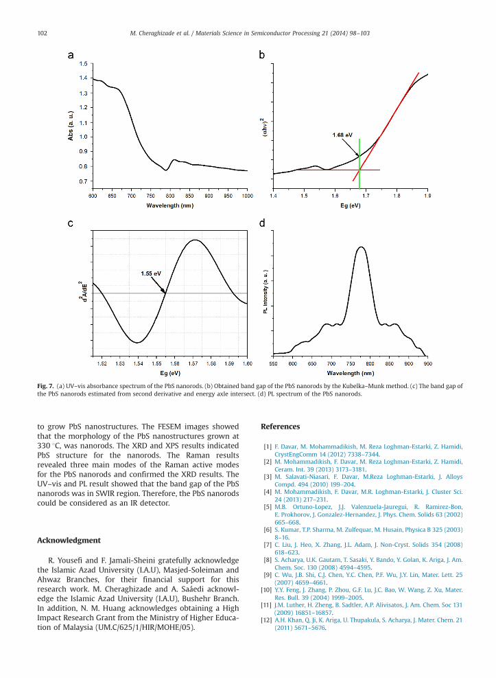
Fig. 7. (a) UV–vis absorbance spectrum of the PbS nanorods. (b) Obtained band gap of the PbS nanorods by the Kubelka–Munk method. (c) The band gap ofthe PbS nanorods estimated from second derivative and energy axle intersect. (d) PL spectrum of the PbS nanorods.
M. Cheraghizade et al. / Materials Science in Semiconductor Processing 21 (2014) 98–103102
to grow PbS nanostructures. The FESEM images showedthat the morphology of the PbS nanostructures grown at330 1C, was nanorods. The XRD and XPS results indicatedPbS structure for the nanorods. The Raman resultsrevealed three main modes of the Raman active modesfor the PbS nanorods and confirmed the XRD results. TheUV–vis and PL result showed that the band gap of the PbSnanorods was in SWIR region. Therefore, the PbS nanorodscould be considered as an IR detector.
Acknowledgment
R. Yousefi and F. Jamali-Sheini gratefully acknowledgethe Islamic Azad University (I.A.U), Masjed-Soleiman andAhwaz Branches, for their financial support for thisresearch work. M. Cheraghizade and A. Saáedi acknowl-edge the Islamic Azad University (I.A.U), Bushehr Branch.In addition, N. M. Huang acknowledges obtaining a HighImpact Research Grant from the Ministry of Higher Educa-tion of Malaysia (UM.C/625/1/HIR/MOHE/05).
References
[1] F. Davar, M. Mohammadikish, M. Reza Loghman-Estarki, Z. Hamidi,CrystEngComm 14 (2012) 7338–7344.
[2] M. Mohammadikish, F. Davar, M. Reza Loghman-Estarki, Z. Hamidi,Ceram. Int. 39 (2013) 3173–3181.
[3] M. Salavati-Niasari, F. Davar, M.Reza Loghman-Estarki, J. AlloysCompd. 494 (2010) 199–204.
[4] M. Mohammadikish, F. Davar, M.R. Loghman-Estarki, J. Cluster Sci.24 (2013) 217–231.
[5] M.B. Ortuno-Lopez, J.J. Valenzuela-Jauregui, R. Ramirez-Bon,E. Prokhorov, J. Gonzalez-Hernandez, J. Phys. Chem. Solids 63 (2002)665–668.
[6] S. Kumar, T.P. Sharma, M. Zulfequar, M. Husain, Physica B 325 (2003)8–16.
[7] C. Liu, J. Heo, X. Zhang, J.L. Adam, J. Non-Cryst. Solids 354 (2008)618–623.
[8] S. Acharya, U.K. Gautam, T. Sasaki, Y. Bando, Y. Golan, K. Ariga, J. Am.Chem. Soc. 130 (2008) 4594–4595.
[9] C. Wu, J.B. Shi, C.J. Chen, Y.C. Chen, P.F. Wu, J.Y. Lin, Mater. Lett. 25(2007) 4659–4661.
[10] Y.Y. Feng, J. Zhang, P. Zhou, G.F. Lu, J.C. Bao, W. Wang, Z. Xu, Mater.Res. Bull. 39 (2004) 1999–2005.
[11] J.M. Luther, H. Zheng, B. Sadtler, A.P. Alivisatos, J. Am. Chem. Soc 131(2009) 16851–16857.
[12] A.H. Khan, Q. Ji, K. Ariga, U. Thupakula, S. Acharya, J. Mater. Chem. 21(2011) 5671–5676.

M. Cheraghizade et al. / Materials Science in Semiconductor Processing 21 (2014) 98–103 103
[13] R.S. Kane, R.E. Cohen, R. Silbey, J. Phys. Chem. 100 (1996) 7928–7932.[14] M. Yousefi, F. Gholamian, D. Ghanbari, M. Salavati-Niasari, Polyhe-
dron 30 (2011) 1055–1060.[15] S.B. Pawar, J.S. Shaikh, R.S. Devan, Y.R. Ma, D. Haranath, P.N. Bhosale,
P.S. Patil, Appl. Surf. Sci. 258 (2011) 1869–1875.[16] S. Xiong, B. Xi, D. Xu, C. Wang, X. Feng, H. Zhou, Y. Qian, J. Phys.
Chem. C 111 (2007) 16761–16767.[17] J. Bu, C. Nie, J. Liang, L. Sun, Z. Xie, Q. Wu, C. Lin, Nanotechnology 22
(2011) 125602.[18] A.K. Singh, G.S. Thool, S.R. Deo, R.S. Singh, A. Gupta, Res. Chem.
Intermed. 38 (2012) 2041–2049.[19] A.I. Kovalev, D.L. Wainstein, A.Yu. Rashkovskiy, A. Osherovb,
Y. Golanb, Surf. Interface Anal. 42 (2010) 850–854.[20] Y. Ni, H. Liu, F Wang, Y. Liang, J. Hong, X. Ma, Z. Xu, Cryst. Res.
Technol. 39 (2004) 200–206.[21] S. Wang, A. Pan, H. Yin, Y. He, Y. Lei, Z. Xu, B. Zou, Mater. Lett. 60
(2006) 1242–1246.
[22] H. Cao, G. Wang, S. Zhang, X. Zhang, Nanotechnology 17 (2006)3280–3287.
[23] Y. H Zhang, L. Guo, P.G. Yin, R. Zhang, Q. Zhang, S.H. Yang, Chem. Eur.J. 13 (2007) 2903–2907.
[24] J. Akhtar, M. Azad Malik, P. O’Brien, K.G.U. Wijayantha, R. Dharmadasa,S.J.O. Hardman, D.M. Graham, B.F. Spencer, S.K. Stubbs, W.R. Flavell,D.J. Binks, F. Sirotti, M.E. Kazzi, M. Silly, J. Mater. Chem. 20 (2010)2336–2344.
[25] A. Khorsand Zak, R. Yousefi, W.H. Abd Majid, M.R. Muhamad, Ceram.Int. 38 (2012) 2059–2064.
[26] M. Mohammadikish, F. Davar, M.R. Loghman-Estarki, Z. Hamidi,Ceram. Int. 39 (2013) 3173–3181.
[27] A. Khorsand Zak, R. Razali, W.H. Abd Majid, M. Darroudi, Int. J.Nanomed. 6 (2011) 1399–1403.