large band gap opening between graphene dirac cones ... · between the π and π* states. several...
TRANSCRIPT

PAPAGNO ET AL. VOL. XXX ’ NO. XX ’ 000–000 ’ XXXX
www.acsnano.org
A
CXXXX American Chemical Society
Large Band Gap Opening betweenGraphene Dirac Cones Induced byNa Adsorption onto an Ir SuperlatticeMarco Papagno,†,* Stefano Rusponi,‡ Polina Makarovna Sheverdyaeva,† Sergio Vlaic,‡ Markus Etzkorn,‡
Daniela Pacile,†,§ Paolo Moras,† Carlo Carbone,† and Harald Brune‡
†Istituto di Struttura della Materia, Consiglio Nazionale delle Ricerche, Trieste, Italy, ‡Institute of Condensed Matter Physics (ICMP), Station 3, Ecole PolytechniqueFédérale de Lausanne (EPFL), CH-1015 Lausanne, Switzerland, and §Dipartimento di Fisica, Università della Calabria, and INFN-Gruppo collegato di Cosenza,87036 Arcavacata di Rende (CS), Italy
Graphene (G) exhibits several exoticproperties that can be ascribed to itstwo-dimensional character and band
topology.1�6 In native, freestanding gra-phene (Figure 1a), the π and π* states dis-perse linearly in the proximity of the Fermilevel (EF) and define the so-called Diraccones, which are centered at the K-pointsof the reciprocal space and degenerate atthe Dirac energy (ED), where the cone verti-ces meet. This band structure, and the relat-ed high electron mobility, makes grapheneappealing for nanoelectronics. Since gra-phene is a semiconductor with zero bandgap (Δ), the very first requisite for the ex-ploitation of graphene for logic device ap-plications consists in opening a band gapbetween the π and π* states. Several meth-ods exist to achieve this goal. Cutting gra-phene into stripes (graphene nanoribbons)is an efficient way to break the degeneracyat ED.
7�9 Recently,10 the bottom-up ap-proach has led to the production of nano-ribbons with uniform width and well-definededges; however, the extension of this meth-od to semiconductor substrates remainschallenging. Alternatively, the tunable bandgap in gated graphene bilayers rangingfrom 0 to 250 meV may enable novel nano-electronic and nanophotonic devices.11
Angle-resolved photoemission spectros-copy (ARPES) experiments12 show, however,that the band structure of these systemsdoes not fulfill the requirement of high elec-tron group velocity. Patterning,13�15 adsorp-tion16�18 and intercalation of suitable ele-ments,19,20 strain,21,22 or substrate-inducedsymmetry breaking23�25 are other techni-ques inducing band gaps in graphene layersranging from a few tens to a few hundredsofmillielectronvolts. In this context,metal sub-strates to which graphene couples weakly,
such as Pt(111)26 and Ir(111),27 offer inter-esting opportunities. Due to the large G/substrate spacing (about 3.7 Å), the bandtopology of the Dirac cones is weakly per-turbed in these systems,24,28 at variancewith the case of strongly interacting metals(Ni(111),29 Ru(0001)30,31), where the spacingis reduced to about 2.1 Å. Graphene is thusrelatively well decoupled from the Ir(111)substrate, and in fact, the high group veloc-ity of its charge carriers is preserved.24 Thelattice mismatch between graphene and Irresults in a long-period moiré superstruc-ture, which weakly modulates the crystalpotential and affects the electronic bands ofgraphene.24,32,33 This results in the openingof a small band gap of about 140 meV be-tween the π and π* states at the K-point ofthe graphene Brillouin zone (see Figure 1b).These states can be further modified byordered adsorption of atomic hydrogen18 orIr clusters.24 H and Ir atoms selectively adsorbon the hexagonal close-packed (hcp) regions
* Address correspondence [email protected].
Received for review September 1, 2011and accepted December 3, 2011.
Published online10.1021/nn203841q
ABSTRACT We investigate the effects of
Na adsorption on the electronic structure
of bare and Ir cluster superlattice-covered
epitaxial graphene on Ir(111) using angle-
resolved photoemission spectroscopy and scan-
ning tunneling microscopy. At Na saturation
coverage, a massive charge migration from
sodium atoms to graphene raises the gra-
phene Fermi level by ∼1.4 eV relative to its
neutrality point. We find that Na is adsorbed on top of the graphene layer, and when
coadsorbed onto an Ir cluster superlattice, it results in the opening of a large band gap of
ΔNa/Ir/G = 740 meV, comparable to the one of Ge and with preserved high group velocity of the
charge carriers.
KEYWORDS: Na absorption . Ir superlattice . graphene . photoemission . STM
ARTIC
LE
PAPAGNO ET AL. VOL. XXX ’ NO. XX ’ 000–000 ’ XXXX
www.acsnano.org
B
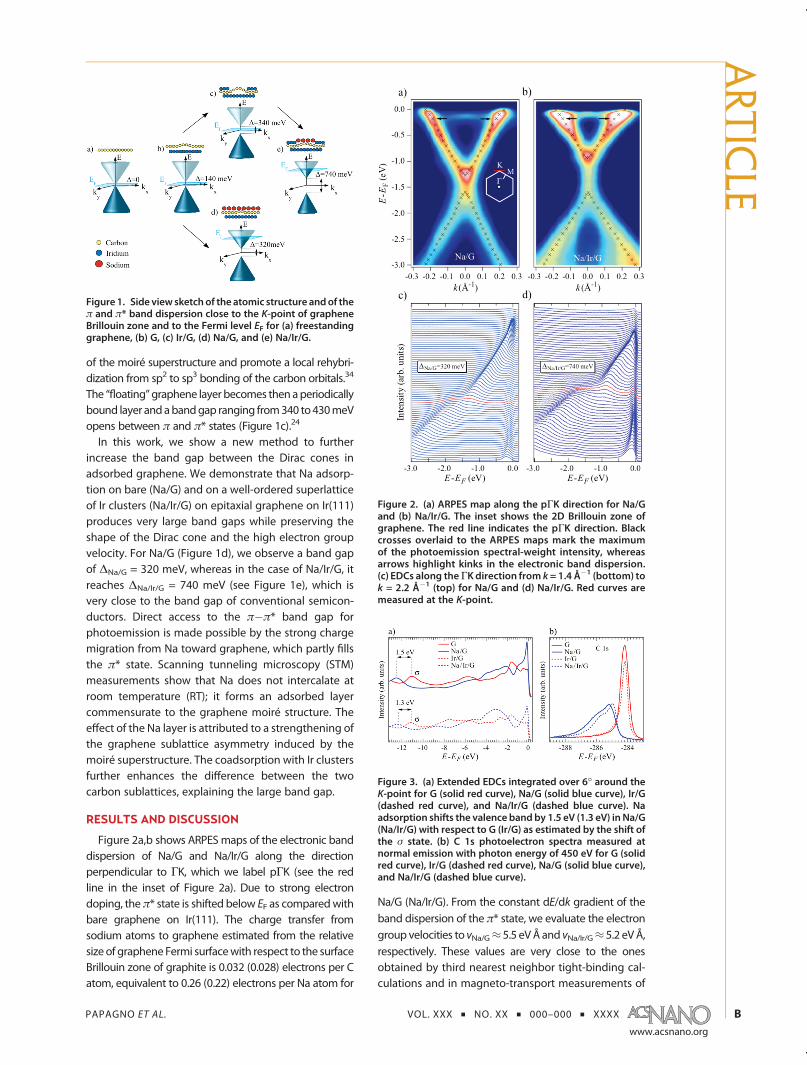
of the moiré superstructure and promote a local rehybri-dization from sp2 to sp3 bonding of the carbon orbitals.34
The “floating”graphene layer becomes thenaperiodicallybound layer andabandgap ranging from340 to430meVopens between π and π* states (Figure 1c).24
In this work, we show a new method to furtherincrease the band gap between the Dirac cones inadsorbed graphene. We demonstrate that Na adsorp-tion on bare (Na/G) and on a well-ordered superlatticeof Ir clusters (Na/Ir/G) on epitaxial graphene on Ir(111)produces very large band gaps while preserving theshape of the Dirac cone and the high electron groupvelocity. For Na/G (Figure 1d), we observe a band gapof ΔNa/G = 320 meV, whereas in the case of Na/Ir/G, itreaches ΔNa/Ir/G = 740 meV (see Figure 1e), which isvery close to the band gap of conventional semicon-ductors. Direct access to the π�π* band gap forphotoemission is made possible by the strong chargemigration from Na toward graphene, which partly fillsthe π* state. Scanning tunneling microscopy (STM)measurements show that Na does not intercalate atroom temperature (RT); it forms an adsorbed layercommensurate to the graphene moiré structure. Theeffect of the Na layer is attributed to a strengthening ofthe graphene sublattice asymmetry induced by themoiré superstructure. The coadsorption with Ir clustersfurther enhances the difference between the twocarbon sublattices, explaining the large band gap.
RESULTS AND DISCUSSION
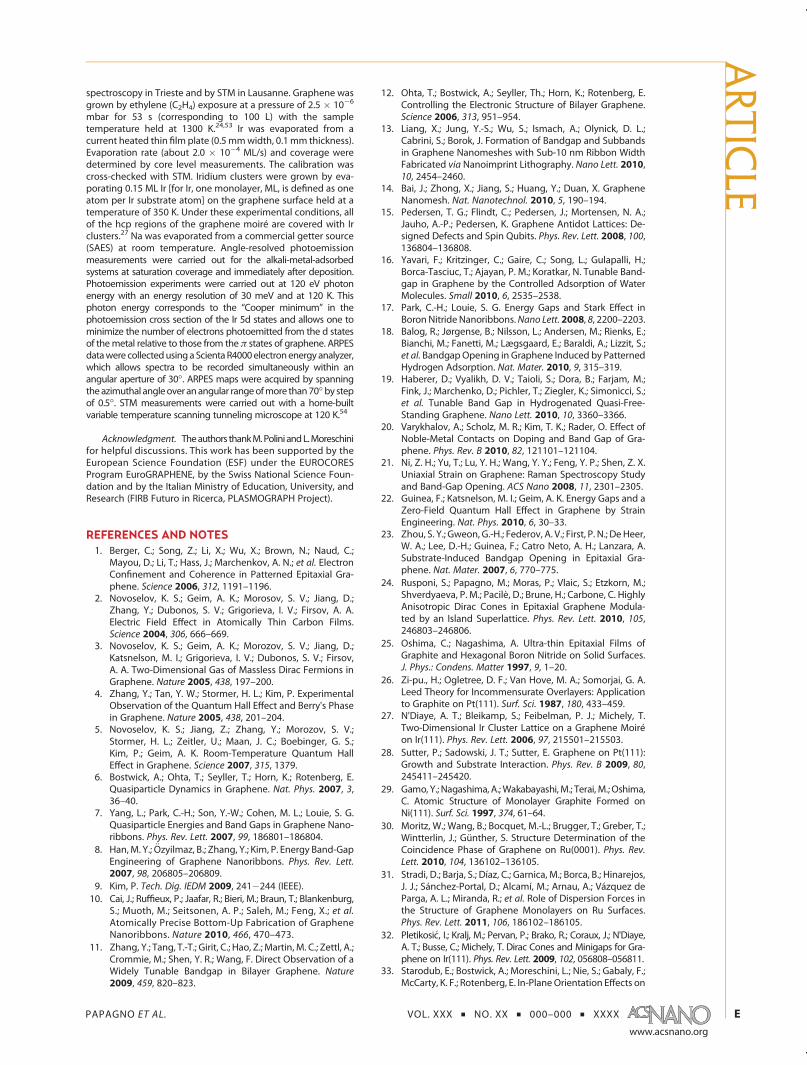
Figure 2a,b shows ARPES maps of the electronic banddispersion of Na/G and Na/Ir/G along the directionperpendicular to ΓK, which we label pΓK (see the redline in the inset of Figure 2a). Due to strong electrondoping, theπ* state is shifted below EF as comparedwithbare graphene on Ir(111). The charge transfer fromsodium atoms to graphene estimated from the relativesize of graphene Fermi surfacewith respect to the surfaceBrillouin zone of graphite is 0.032 (0.028) electrons per Catom, equivalent to 0.26 (0.22) electrons per Na atom for
Na/G (Na/Ir/G). From the constant dE/dk gradient of theband dispersion of the π* state, we evaluate the electrongroup velocities to vNa/G≈ 5.5 eVÅand vNa/Ir/G≈ 5.2 eVÅ,respectively. These values are very close to the onesobtained by third nearest neighbor tight-binding cal-culations and in magneto-transport measurements of
Figure 2. (a) ARPES map along the pΓK direction for Na/Gand (b) Na/Ir/G. The inset shows the 2D Brillouin zone ofgraphene. The red line indicates the pΓK direction. Blackcrosses overlaid to the ARPES maps mark the maximumof the photoemission spectral-weight intensity, whereasarrows highlight kinks in the electronic band dispersion.(c) EDCs along theΓK direction from k= 1.4 Å�1 (bottom) tok = 2.2 Å�1 (top) for Na/G and (d) Na/Ir/G. Red curves aremeasured at the K-point.
Figure 3. (a) Extended EDCs integrated over 6� around theK-point for G (solid red curve), Na/G (solid blue curve), Ir/G(dashed red curve), and Na/Ir/G (dashed blue curve). Naadsorption shifts the valence band by 1.5 eV (1.3 eV) in Na/G(Na/Ir/G) with respect to G (Ir/G) as estimated by the shift ofthe σ state. (b) C 1s photoelectron spectra measured atnormal emission with photon energy of 450 eV for G (solidred curve), Ir/G (dashed red curve), Na/G (solid blue curve),and Na/Ir/G (dashed blue curve).
Figure 1. Side view sketch of the atomic structure andof theπ and π* band dispersion close to the K-point of grapheneBrillouin zone and to the Fermi level EF for (a) freestandinggraphene, (b) G, (c) Ir/G, (d) Na/G, and (e) Na/Ir/G.
ARTIC
LE

PAPAGNO ET AL. VOL. XXX ’ NO. XX ’ 000–000 ’ XXXX
www.acsnano.org
C
freestanding graphene.35 For both systems, theπ* (π) state disperses linearly downward (upward)and reaches a minimum (maximum) at the grapheneK-point. There, π and π* states open up a band gap ofΔNa/G = 320meV for Na/G and ofΔNa/Ir/G = 740meV fortheNa/Ir/G surface. The energy distribution curves (EDCs)along the ΓK direction are shown in Figure 2c,d andreveal broad line shapes, which cause an overlap ofthe intensity tails from the top of the valence band andthe bottom of the conduction band. Nevertheless, thedispersion of the bands and the electronic gap be-tween the π and π* states are well resolved.The graphene π* state exhibits a kink at about
180 meV below EF highlighted by arrows in Figure 2a,b.Similarly to K-doped graphene/Ir,36 this feature can beinterpreted as a renormalization of theDirac cone bandintroducedby electron�phonon interactions; however,the overlap between Ir 5d and Gπ states near EF
33 doesnot allow an unequivocal assignment.Extended EDCs integrated over 6� around the K-point
in Figure3a allowquantifying the shift of graphenebands.In particular, from the displacement of the σ band, wemeasure a downward shift of 1.5 eV for Na/G (blue fullcurve) and 1.3 eV for Na/Ir/G (blue dashed curve) as com-pared to the undoped surfaces displayed in red. Thesevalues are in good agreementwith experimental observa-tions on K-doped graphene on Ir(111)36 and KC8
37 andwith the theoretical prediction for Li-doped graphene.38
Figure 4a,b shows STM images of the bare and partlyNa covered graphene, respectively, demonstratingthat Na does not intercalate at RT but rather decoratesthe step edges and forms single-layer islands withlateral dimensions that vary from 10 to 100 nm for acoverage of θ ∼ 0.5 ML.39 Note that the adsorptionproperties of Na on graphite significantly differ fromthe other alkali metals, and Na does not form inter-calation compounds while the other alkalis do.40 Thissingular behavior seems to be present also on metal-supported graphene. In contrast to Na, K has beenreported to penetrate the graphene layer on Ni(111)already at RT and to act as a spacer.41,42 In these sys-tems, the increased distance reduces the hybridizationbetween Ni 3d and C 2pz states and forces the disper-sion of the π band to turn from parabolic to linear.For our system, we observe that the Na island size
increases with exposure time until the whole graphenesurface is covered for θ = 1 ML. Alkali metals on gra-phite possess a “correlated liquid” phase in the low-coverage regime. This phase originates from the chargetransfer from the alkalis to the graphite leading to verticaldipoleswhich repel each other, preventing the formationof islands and maximizing the adatom�adatom dis-tance.43,44 As the alkali coverage reaches a critical density,a nucleation to amore closely packed configuration is ob-served, which results in the formation of alkali islandsalmost decoupled from the substrate. In our case,we observe island formation from lowest coverage on,
reminiscent of an attractive interaction between Naadatoms. In analogy with K36,45 and Li38,46 on graphene,Na is expected to form a (2 � 2) or (
√3 � √
3)R30�phase. We were unable to reveal the Na superstructure,presumably due to the weakness of the Na�C bondwith respect to interaction with the STM tip oftenresulting in tip-induced displacements of Na atoms.However, for particular tunneling conditions, the Nalayer appears transparent and the moiré pattern of theunderlying graphene with attenuated corrugation ap-pears in the STM images, revealing that Na adsorp-tion does not change the graphene moiré structure.We further find that the edges of the Na islands arealways aligned to those of the underlying graphenemoiré superstructure, thus suggesting a Na superstruc-ture commensurate with that of the graphene moiré.From the fact that the moiré unit cell contains close to(10 � 10) graphene unit cells above a (9 � 9) Ir(111)unit cell,27 we conclude a (2 � 2) Na superstructure.Further support for the (2� 2) Na/G phase is provided
by core levelmeasurements. In Figure 3b, we report the C1s peak for bare graphene (red full curve) centeredat �284.15 eV below EF, in agreement with earlier re-sults.47,48 Following Na adsorption (full blue curve), weobserve a shift of themainpeakby1.05eV toward higherbinding energy and a shoulder at∼�286 eV. The samesplitting has been observed for (2 � 2) K/graphite and
Figure 4. (a) Constant current STM image showing themoiré pattern of clean graphene on Ir(111) (tunnel voltageapplied to sample Vt = 0.05 V; tunnel current It = 10 nA; size72 nm � 72 nm). (b) Graphene covered by Na patches for aNa coverage θ≈ 0.5ML (Vt =�2.5 V; It = 10 nA; size 56 nm�56 nm).
Figure 5. Constant-energy ARPES maps at (a) E�EF =400 meV for G and (b) E�EF = 530 meV Ir/G. Dashed linemarks the first graphene Brillouin zone. Main Dirac cone islabeled “0”, whereas “1�6” are replicas. In (b), only threeout of six replicas are observed.
ARTIC
LE

PAPAGNO ET AL. VOL. XXX ’ NO. XX ’ 000–000 ’ XXXX
www.acsnano.org
D
assigned to energy losses associated with the metallicoverlayer.49 We therefore suggest that this shoulder isdue to energy losses associated with (2 � 2) Na.The presence of Ir clusters on graphene induces
small changes to the line shape of the C 1s resonance(dashed red curve in Figure 3b). Na deposition on thecluster superlattice (dashed blue curve) also producesa downward shift of the C 1s peak, which is howeverreduced by ∼200 meV with respect to the shift ob-served in Na/G. We attribute this effect to the smallersaturation coverage of sodium at the Ir/G surface causedbysite blocking. Similar line shapesof thephotoemissionspectra for the Na-covered surface, with andwithout thecluster superlattice, suggest that, for the sodium satura-tion coverage, the presence of Ir clusters only weaklyaffects the adsorption properties of Na.In graphene supported on Ni(111) and in graphite,
alkali metal intercalation is supposed to happen at surfacedefects suchas stepedgesorwalls betweendifferent rota-tional domains.41,50 In our case, the high quality of the gra-phene layer with and without the Ir clusters may preventNa intercalation. Figure 5a,b shows constant-energyARPES maps for G and Ir/G, respectively. The G/Ir(111)moiré superpotential32 induces six replicas of the πstate, labeled “1�6”, surrounding the main Dirac cone,“0”, centered at the K-point. The Ir cluster superlatticeintroduces anisotropies in the spectral-weight distribu-tion by suppressing the photoemission intensity ofthree of the six replicas, but it does not affect thequality of the graphene layer.24 The absence of addi-tional Dirac cones rotated away from the K-points alsorules out rotational domains33 in both surfaces.We propose two possible origins of the observed band
gaps. First, Na adatoms modify the crystal potential, thusΔNa/G is expected to be different from that of undopedgraphene. Previous photoemission experiments of Na onhighly oriented pyrolytic graphite revealed the presenceof an energy gap in the surface electronic structure.51 Thisband gap has been attributed to an inhomogeneouscharge transfer through the stack of the graphene layers,which perturbs the symmetry of the graphite lattice.Similarly, we may argue in the present case that, upondeposition of Na, the electronic charge is differently dis-tributedbetween the grapheneoverlayer and themetallicsubstrate modifying the symmetry of the system.The second possibility is related to the commensurate
phase of Na adatomswith respect to the graphenemoiré.It has been found theoretically38 that a (2 � 2) super-structure of any adsorbate on an unperturbed graphenelayer should not open a band gap, as the (2 � 2) phase
does not break the degeneracy of the two carbonsublattices, and in fact, no gap has been experimentallyreported on any (2 � 2) phase on graphene on SiC.6,45,52
However, the graphenemoiré on Ir(111) breaks this dege-neracy for2/3of thegraphene layerwhereeitheroneof thetwo C atoms is adsorbed on top an Ir atom, whereas theother is located on a three-fold hollow site.27 Accordingly,there is a small electronic gap at the K-point.24,32,33 The as-grown (2 � 2) Na superstructure can enhance this differ-encebetween theC sublattices and thus increase the bandgap. TheC sublatticedegeneracy canalsobe lifted throughIr clustersdue to thepeculiarpropertiesof the Ir adatoms tonucleate only on the hcp sites of themoiré and due to thelocal rehybridization of the C atoms.27,34 The combinationof Ir clusters and Na atoms induces the strongest breakingof the C sublattice degeneracy and leads to the large bandgap of ΔNa/Ir/G = 740 meV.
CONCLUSION
We have demonstrated that Na adsorption onto bareand Ir cluster superlattice-precovered epitaxial grapheneon Ir(111) produces very large band gaps between the πandπ* states amounting toΔNa/G=320meVandΔNa/Ir/G=740meV, respectively. The latter is comparablewith thatofGe. In addition, we find that the linear band dispersion isonly marginally perturbed, giving rise to electron groupvelocities close to the ones of freestanding graphene.Photoemission experiments show that there is a substan-tial charge transfer fromNa tographenewhichpromotesadownward shift of electronic states by more than 1 eV.STM data show that Na is adsorbed on top of graphene,most likely in a (2� 2) phase, and does not intercalate atRT. Though a (2 � 2) reconstruction is not expected toremove the degeneracy between graphene states at theK-point, a band gap may be induced by a hybridizationbetween the electron wave functions with wave vectors Kand K0 promoted by the translation symmetry breaking ofthe combined Na-graphene-Ir(111) lattice. We attributethewideΔNa/Ir/Gbandgap toamutualphenomenonofNaand Ir which breaks the degeneracy of the two sublatticesof graphene. This combined effect may apply to systemsother than graphene on Ir. The prerequisites for ourmethod to work are a graphene moiré pattern acting astemplate for the growth of nanostructure superlatticesand an ordered array of dopant that does not intercalate.Therefore, a transfer to SiC is, in principle, feasible sincealso this systemexhibits amoiré pattern and alkalis donotintercalate at RT.6,45,46 Our method has the advantage toopen large band gaps in the electronic states while pre-serving the appealing transport properties of graphene.
METHODSThe ARPES experiments were performed at the VUV-Photo-
emission beamline at Elettra in Trieste and the STM experimentsat EPFL under ultrahigh vacuum (UHV) condition with a base
pressure better than 5 � 10�11 mbar. The Ir(111) crystal wascleaned by repeated cycles of Arþ sputtering (E = 1.2 keV) andannealing at T=1500 K. Order and cleanness of the samplewere
monitored by low-energy electron diffraction and photoemission
ARTIC
LE
PAPAGNO ET AL. VOL. XXX ’ NO. XX ’ 000–000 ’ XXXX
www.acsnano.org
E
spectroscopy in Trieste and by STM in Lausanne. Graphene wasgrown by ethylene (C2H4) exposure at a pressure of 2.5 � 10�6
mbar for 53 s (corresponding to 100 L) with the sampletemperature held at 1300 K.24,53 Ir was evaporated from acurrent heated thin film plate (0.5mmwidth, 0.1mm thickness).Evaporation rate (about 2.0 � 10�4 ML/s) and coverage weredetermined by core level measurements. The calibration wascross-checked with STM. Iridium clusters were grown by eva-porating 0.15 ML Ir [for Ir, one monolayer, ML, is defined as oneatom per Ir substrate atom] on the graphene surface held at atemperature of 350 K. Under these experimental conditions, allof the hcp regions of the graphene moiré are covered with Irclusters.27 Na was evaporated from a commercial getter source(SAES) at room temperature. Angle-resolved photoemissionmeasurements were carried out for the alkali-metal-adsorbedsystems at saturation coverage and immediately after deposition.Photoemission experiments were carried out at 120 eV photonenergy with an energy resolution of 30 meV and at 120 K. Thisphoton energy corresponds to the “Cooper minimum” in thephotoemission cross section of the Ir 5d states and allows one tominimize the number of electrons photoemitted from the d statesof themetal relative to those from the π states of graphene. ARPESdatawere collectedusingaScientaR4000electronenergyanalyzer,which allows spectra to be recorded simultaneously within anangular aperture of 30�. ARPES maps were acquired by spanningtheazimuthal angleover anangular rangeofmore than70�bystepof 0.5�. STM measurements were carried out with a home-builtvariable temperature scanning tunneling microscope at 120 K.54
Acknowledgment. Theauthors thankM.Polini andL.Moreschinifor helpful discussions. This work has been supported by theEuropean Science Foundation (ESF) under the EUROCORESProgram EuroGRAPHENE, by the Swiss National Science Foun-dation and by the Italian Ministry of Education, University, andResearch (FIRB Futuro in Ricerca, PLASMOGRAPH Project).
REFERENCES AND NOTES1. Berger, C.; Song, Z.; Li, X.; Wu, X.; Brown, N.; Naud, C.;
Mayou, D.; Li, T.; Hass, J.; Marchenkov, A. N.; et al. ElectronConfinement and Coherence in Patterned Epitaxial Gra-phene. Science 2006, 312, 1191–1196.
2. Novoselov, K. S.; Geim, A. K.; Morosov, S. V.; Jiang, D.;Zhang, Y.; Dubonos, S. V.; Grigorieva, I. V.; Firsov, A. A.Electric Field Effect in Atomically Thin Carbon Films.Science 2004, 306, 666–669.
3. Novoselov, K. S.; Geim, A. K.; Morozov, S. V.; Jiang, D.;Katsnelson, M. I.; Grigorieva, I. V.; Dubonos, S. V.; Firsov,A. A. Two-Dimensional Gas of Massless Dirac Fermions inGraphene. Nature 2005, 438, 197–200.
4. Zhang, Y.; Tan, Y. W.; Stormer, H. L.; Kim, P. ExperimentalObservation of the Quantum Hall Effect and Berry's Phasein Graphene. Nature 2005, 438, 201–204.
5. Novoselov, K. S.; Jiang, Z.; Zhang, Y.; Morozov, S. V.;Stormer, H. L.; Zeitler, U.; Maan, J. C.; Boebinger, G. S.;Kim, P.; Geim, A. K. Room-Temperature Quantum HallEffect in Graphene. Science 2007, 315, 1379.
6. Bostwick, A.; Ohta, T.; Seyller, T.; Horn, K.; Rotenberg, E.Quasiparticle Dynamics in Graphene. Nat. Phys. 2007, 3,36–40.
7. Yang, L.; Park, C.-H.; Son, Y.-W.; Cohen, M. L.; Louie, S. G.Quasiparticle Energies and Band Gaps in Graphene Nano-ribbons. Phys. Rev. Lett. 2007, 99, 186801–186804.
8. Han, M. Y.; €Ozyilmaz, B.; Zhang, Y.; Kim, P. Energy Band-GapEngineering of Graphene Nanoribbons. Phys. Rev. Lett.2007, 98, 206805–206809.
9. Kim, P. Tech. Dig. IEDM 2009, 241�244 (IEEE).10. Cai, J.; Ruffieux, P.; Jaafar, R.; Bieri, M.; Braun, T.; Blankenburg,
S.; Muoth, M.; Seitsonen, A. P.; Saleh, M.; Feng, X.; et al.Atomically Precise Bottom-Up Fabrication of GrapheneNanoribbons. Nature 2010, 466, 470–473.
11. Zhang, Y.; Tang, T.-T.; Girit, C.; Hao, Z.; Martin, M. C.; Zettl, A.;Crommie, M.; Shen, Y. R.; Wang, F. Direct Observation of aWidely Tunable Bandgap in Bilayer Graphene. Nature2009, 459, 820–823.
12. Ohta, T.; Bostwick, A.; Seyller, Th.; Horn, K.; Rotenberg, E.Controlling the Electronic Structure of Bilayer Graphene.Science 2006, 313, 951–954.
13. Liang, X.; Jung, Y.-S.; Wu, S.; Ismach, A.; Olynick, D. L.;Cabrini, S.; Borok, J. Formation of Bandgap and Subbandsin Graphene Nanomeshes with Sub-10 nm Ribbon WidthFabricated via Nanoimprint Lithography. Nano Lett. 2010,10, 2454–2460.
14. Bai, J.; Zhong, X.; Jiang, S.; Huang, Y.; Duan, X. GrapheneNanomesh. Nat. Nanotechnol. 2010, 5, 190–194.
15. Pedersen, T. G.; Flindt, C.; Pedersen, J.; Mortensen, N. A.;Jauho, A.-P.; Pedersen, K. Graphene Antidot Lattices: De-signed Defects and Spin Qubits. Phys. Rev. Lett. 2008, 100,136804–136808.
16. Yavari, F.; Kritzinger, C.; Gaire, C.; Song, L.; Gulapalli, H.;Borca-Tasciuc, T.; Ajayan, P. M.; Koratkar, N. Tunable Band-gap in Graphene by the Controlled Adsorption of WaterMolecules. Small 2010, 6, 2535–2538.
17. Park, C.-H.; Louie, S. G. Energy Gaps and Stark Effect inBoron Nitride Nanoribbons.Nano Lett. 2008, 8, 2200–2203.
18. Balog, R.; Jørgense, B.; Nilsson, L.; Andersen, M.; Rienks, E.;Bianchi, M.; Fanetti, M.; Lægsgaard, E.; Baraldi, A.; Lizzit, S.;et al. BandgapOpening in Graphene Induced by PatternedHydrogen Adsorption. Nat. Mater. 2010, 9, 315–319.
19. Haberer, D.; Vyalikh, D. V.; Taioli, S.; Dora, B.; Farjam, M.;Fink, J.; Marchenko, D.; Pichler, T.; Ziegler, K.; Simonicci, S.;et al. Tunable Band Gap in Hydrogenated Quasi-Free-Standing Graphene. Nano Lett. 2010, 10, 3360–3366.
20. Varykhalov, A.; Scholz, M. R.; Kim, T. K.; Rader, O. Effect ofNoble-Metal Contacts on Doping and Band Gap of Gra-phene. Phys. Rev. B 2010, 82, 121101–121104.
21. Ni, Z. H.; Yu, T.; Lu, Y. H.; Wang, Y. Y.; Feng, Y. P.; Shen, Z. X.Uniaxial Strain on Graphene: Raman Spectroscopy Studyand Band-Gap Opening. ACS Nano 2008, 11, 2301–2305.
22. Guinea, F.; Katsnelson, M. I.; Geim, A. K. Energy Gaps and aZero-Field Quantum Hall Effect in Graphene by StrainEngineering. Nat. Phys. 2010, 6, 30–33.
23. Zhou, S. Y.; Gweon, G.-H.; Federov, A. V.; First, P. N.; De Heer,W. A.; Lee, D.-H.; Guinea, F.; Catro Neto, A. H.; Lanzara, A.Substrate-Induced Bandgap Opening in Epitaxial Gra-phene. Nat. Mater. 2007, 6, 770–775.
24. Rusponi, S.; Papagno, M.; Moras, P.; Vlaic, S.; Etzkorn, M.;Shverdyaeva, P. M.; Pacilè, D.; Brune, H.; Carbone, C. HighlyAnisotropic Dirac Cones in Epitaxial Graphene Modula-ted by an Island Superlattice. Phys. Rev. Lett. 2010, 105,246803–246806.
25. Oshima, C.; Nagashima, A. Ultra-thin Epitaxial Films ofGraphite and Hexagonal Boron Nitride on Solid Surfaces.J. Phys.: Condens. Matter 1997, 9, 1–20.
26. Zi-pu., H.; Ogletree, D. F.; Van Hove, M. A.; Somorjai, G. A.Leed Theory for Incommensurate Overlayers: Applicationto Graphite on Pt(111). Surf. Sci. 1987, 180, 433–459.
27. N'Diaye, A. T.; Bleikamp, S.; Feibelman, P. J.; Michely, T.Two-Dimensional Ir Cluster Lattice on a Graphene Moiréon Ir(111). Phys. Rev. Lett. 2006, 97, 215501–215503.
28. Sutter, P.; Sadowski, J. T.; Sutter, E. Graphene on Pt(111):Growth and Substrate Interaction. Phys. Rev. B 2009, 80,245411–245420.
29. Gamo, Y.; Nagashima, A.; Wakabayashi, M.; Terai, M.; Oshima,C. Atomic Structure of Monolayer Graphite Formed onNi(111). Surf. Sci. 1997, 374, 61–64.
30. Moritz, W.; Wang, B.; Bocquet, M.-L.; Brugger, T.; Greber, T.;Wintterlin, J.; Günther, S. Structure Determination of theCoincidence Phase of Graphene on Ru(0001). Phys. Rev.Lett. 2010, 104, 136102–136105.
31. Stradi, D.; Barja, S.; Díaz, C.; Garnica, M.; Borca, B.; Hinarejos,J. J.; Sánchez-Portal, D.; Alcamí, M.; Arnau, A.; Vázquez deParga, A. L.; Miranda, R.; et al. Role of Dispersion Forces inthe Structure of Graphene Monolayers on Ru Surfaces.Phys. Rev. Lett. 2011, 106, 186102–186105.
32. Pletikosi�c, I.; Kralj, M.; Pervan, P.; Brako, R.; Coraux, J.; N'Diaye,A. T.; Busse, C.; Michely, T. Dirac Cones and Minigaps for Gra-phene on Ir(111). Phys. Rev. Lett. 2009, 102, 056808–056811.
33. Starodub, E.; Bostwick, A.; Moreschini, L.; Nie, S.; Gabaly, F.;McCarty, K. F.; Rotenberg, E. In-PlaneOrientation Effects on
ARTIC
LE

PAPAGNO ET AL. VOL. XXX ’ NO. XX ’ 000–000 ’ XXXX
www.acsnano.org
F
the Electronic Structure, Stability, and Raman Scatteringof Monolayer Graphene on Ir(111). Phys. Rev. B 2011, 83,125428–125436.
34. Feibelman, P. J. Pinning of Graphene to Ir(111) by Flat IrDots. Phys. Rev. B 2008, 77, 165419–165425.
35. Reich, S.; Maultzsch, J.; Thomsen, C.; Ordej�on, P. Tight-Binding Description of Graphene. Phys. Rev. B 2002, 66,035412–035416.
36. Bianchi, M.; Rienks, E. D.; Lizzit, S.; Baraldi, A.; Balog, R.;Hornekaer, L.; Hofmann, Ph. Electron�Phonon Coupling inPotassium-Doped Graphene: Angle-Resolved Photoemis-sion Spectroscopy.Phys. Rev. B 2010, 81, 041403–041406(R).
37. Grüneis, A.; Attaccalite, A.; Rubio, A.; Vyalikh, D. V.; Molodt-sov, S. L.; Fink, J.; Follath, R.; Eberhrdt, W.; Pichler, T.Electronic Structure and Electron�Phonon Coupling ofDoped Graphene Layers in KC8. Phys. Rev. B 2009, 79,205106–205114.
38. Farjam, M.; Rafii-Tabar, H. Energy Gap Opening in Sub-monolayer Lithium onGraphene: Local Density Functionaland Tight-Binding Calculations. Phys. Rev. B 2009, 79,045417–045423.
39. The Na coverage is definedwith respect to a saturatedML.40. Johnson, M. T .; Starnberg, H. I.; Hughes, H. P. Electronic
Structure of Alkali Metal Overlayers on Graphite. Surf. Sci.1986, 178, 290–299.
41. Nagashima, A.; Tejima, N.; Oshima, C. Electronic States ofthe Pristine and Alkali-Metal-Intercalated Monolayer Gra-phite/Ni(111) Systems. Phys. Rev. B 1994, 50, 17487–17495.
42. Grüneis, A.; Vyalikh, D. V. Tunable Hybridization betweenElectronic States of Graphene and a Metal Surface. Phys.Rev. B 2008, 77, 193401–193404.
43. Hunt, M. R. C.; Palmer, R. E. The Development of MetallicBehaviour in Clusters on Surfaces. Philos. Trans. R. Soc.London, Ser. A 1998, 356, 231–247.
44. Yin, F.; Akola, J.; Koskinen, P.; Mannine, M.; Palmer, R. E.Bright BeachesofNanoscale Potassium Islands onGraphitein STM Imaging. Phys. Rev. Lett. 2009, 102, 106102–106105.
45. McChesney, J. L.; Bostwick, A.; Otha, T.; Seyller, T.; Horn, K.;González, J.; Rotenberg, E. Extended van Hove Singularityand Superconducting Instability in DopedGraphene. Phys.Rev. Lett. 2010, 104, 136803–136807.
46. Virojanadara, C.; Watcharinyanon, S.; Zakharov, A. A.;Johansson, L. I. Epitaxial Graphene on 6H-SiC and Li Inter-calation. Phys. Rev. B 2010, 82, 205402–205407.
47. Lizzit, S.; Zampieri, G.; Petaccia, L.; Larciprete, R.; Lacovig, P.;Rienks, E. D. L.; Bihlmayer, G.; Baraldi, A.; Hofmann, P. BandDispersion in the Deep 1s Core Level of Graphene. Nat.Phys. 2010, 6, 345–349.
48. Preobrajenski, A. B.; Ng, M. L.; Vinogradov, A. S.; Mårtensson,N. Controlling Graphene Corrugation on Lattice-Mismatc-hed Substrates. Phys. Rev. B 2008, 78, 073401–073404.
49. Bennich, P.; Puglia, C.; Brühwiler, P. A.; Nilsson, A.; Maxwell,A. J.; Sandell, A.; Mårtensson, N.; Rudolf, P. PhotoemissionStudy of K on Graphite. Phys. Rev. B 1999, 59, 8292–8304.
50. Wu, N. J.; Ignatiev, A. Potassium Absorption into the Gra-phite(0001) Surface: Intercalation. Phys. Rev. B 1983, 28,7288–7293.
51. Pivetta, M.; Patthey, F.; Barke, I.; Hövel, H.; Delley, B.;Schneider, W. D. Gap Opening in the Surface ElectronicStructure of Graphite Induced by Adsorption of AlkaliAtoms: Photoemission Experiments and Density Func-tional Calculations. Phys. Rev. B 2005, 71, 165430–165433.
52. Hwang, C. G.; Shin, S. Y.; Choi, S.-M.; Kim, N. D.; Uhm, S. H.;Kim, H. S.; Hwang, C. C.; Noh, D. Y.; Jhi, S.-H.; Chung, J. W.Stability of Graphene Band Structures Against an ExternalPeriodic Perturbation: Na on Graphene. Phys. Rev. B 2009,79, 115439–115443.
53. N'Diaye, A. T.; Coraux, J.; Plasa, T.; Busse, C.; Michely, T.Structure of Epitaxial Graphene on Ir(111). New J. Phys.2008, 10, 043033–043047.
54. Lehnert, A.; Buluschek, P.; Weiss, N.; Giesecke, J.; Treier, M.;Rusponi, S.; Brune, H. High Resolution In Situ Magneto-Optic Kerr Effect and Scanning Tunneling MicroscopySetup with All Optical Components in UHV. Rev. Sci.Instrum. 2009, 80, 023902–023908.
ARTIC
LE