laplace transfer function simulation with spice
TRANSCRIPT

Page 1 of 37
Laplace Transfer Function Simulation with SPICE
Mark Sitkowski Design Simulation Systems Ltd http://www.designsim.com.au
Introduction
We present a method of expressing a Laplace transfer function in terms of SPICE simulation primitives, such that the effect of the transfer function on an input signal can be directly simulated in SPICE. We derive generic second and third order models, which may be interconnected to simulate more complex systems. Research into this subject is still continuing, and this is the fourth in what has turned out to be a series of re-writes of the original paper, as more results became available. The previous updates filled in the gaps in the theory behind the design of the 1/s integrator, which is key to the accurate simulation of the second and third order systems being considered. Also, we added a detailed analysis and design of third order systems, using the Chebyshev Type 1 filter as an example. The current update adds a section on the simulation of complete PID controlled servo systems, albeit controlling just a simple DC motor. Since Laplace transforms are used almost exclusively in the design and analysis of second and higher order systems, we use the parallel and series tuned circuits, together with the third order Chebyshev filter, to illustrate the design of the model. These results may be extended to higher order systems, by cascading second and third order models, with the added advantage of not having to find the roots of quartic, quintic and higher order equations. In each case, we detail the steps necessary to represent the transfer function in terms of SPICE primitives.
Overview
The transfer function of a system is a frequency-dependent expression which, when multiplied by an input signal, describes the output of that system when driven by that input signal, and may be defined as:
H(s) = Y(s) / U(s) where Y(s) is the Laplace transform of the output, and U(s) is the Laplace transform of the input. An example of a typical transfer function for a third order system could be: (0.5s3 + 1.6s2 + 4.4s + 16) H(s) = ------------------------------------- (s
3 + 6.2s
2 + 7s + 8)
It may be seen that the form of both numerator and denominator is a polynomial expression, where the numerator can be represented by: Y(s) = B0s
m + B1sm-1 + B2s
m-2 + Bm while the denominator looks like: U(s) = A0s
n + A1sn-1 + A2s
n-2 + An

Page 2 of 37
The modelling in SPICE of the summation of terms multiplied by coefficients is a fairly simple operation, so we turn our attention to effect of the powers of ‘s’. For a realisable system, the order of the numerator will be less than or equal to the order of the denominator. If we divide our numerator and denominator by the highest power of ‘s’ present in the denominator, the value of our transfer function will remain the same, and we will have converted all powers of ‘s’ to negative powers of ‘s’. The effect on our hypothetical transfer function, mentioned earlier would be: (0.5 + 1.6s-1 + 4.4s-2 + 16s-3)
H(s) = -------------------------------------- (1 + 6.2s-1 + 7s-2 + 8s-3) The importance of this is that s-1, i.e 1/s, is the Laplace representation of an integrator, so we now have a polynomial with coefficients, each multiplied by an integration function of ascending order, where 1/s is first-order integration, 1/s2 is second-order and so on. Hence, it may be seen that a typical numerator might be represented by: Y(s) = B0 + B1*(1/s) + B2*(1/s2) + B3*(1/s3) + B4*(1/s4) where we have intentionally written 1/sn to emphasise the use of the integration function.
The corresponding denominator would be of the form: U(s) = A0 + A1*(1/s1) + A2*(1/s2) + A3*(1/s3) + A4*(1/s4) It will be noted that, since we divided by the highest power of ‘s’, A0 and B0 will each just be a numerical coefficient, if such exists in the original expression. Assuming that our transfer function, H(s), will operate on an arbitrary input signal V(s), we can express Y(s) as Y(s) = V(s) * U(s) Y(s) = V(s)*A0 + V(s)*A1*(s
-1) + V(s)*A2*(s-2) + V(s)*A3*(s
-3) + V(s)*A4*(s-4) etc.
For our purposes, the above may be written: V(s)*A0 = Y(s) - V(s)*A1*(s
-1) - V(s)*A2*(s-2) - V(s)*A3*(s
-3) - V(s)*A4*(s-4) etc.
Whence, it may be seen that A0 is just a scaling factor, which may be applied to the output signal, or merely ignored. Importantly, since we divide by the highest power of ‘s’ in the denominator, A0 will never be zero, but will be unity, or some other constant. For our hypothetical transfer function, we would obtain the following coefficients: B0 = 0.5 B1 = 1.6 B2 = 4.4 B3 = 16 A0 = 1 * This may be ignored, since it does not appear in the model equation A1 = 6.2 A2 = 7 A3 = 8

Page 3 of 37
If you’re interested in how such a transfer function actually performs, the AC and transient analysis results are in Appendix 4. In summary, it will be noted that each term of the numerator may be represented by an integration and a multiplication by a constant, such that the whole expression may be seen to be a serial summation of such terms, subtracted from the denominator. The creation of integrator, adder and multiplier elements in SPICE is a trivial matter, and a block diagram of the first two terms of such a polynomial is shown if Figure 1. Basically, as the order of the polynomial increases, we extend our model by concatenating additional integrators plus multipliers for the additional numerator and denominator terms, and extending the number of inputs to the front and back end adders. Since B0 only exists as the first term, it is set to zero on the concatenated models of subsequent terms. At this point, there is a temptation to create a module which may be cascaded to create higher order polynomials, which we will resist. Many of the functions with which we are dealing are of either second order or third order, so it is just as convenient to create a second order and a third order template, and merely plug in the coefficients of a given transfer function. These second and third order templates may then themselves be cascaded, to simulate complex systems interacting with each other. This approach yields a less confusing and less cluttered circuit diagram than one created from many first order functions, with discrete adders and multipliers added externally.
MULTIPLY BY A1
MULTIPLY BY B0
MULTIPLY BY B1
INTEGRATE
ADD
ADD
Vin Vout
E(s)
1/s
B0
B1
A1
Figure 1

Page 4 of 37
The output of the front-end adder may be seen to be B0*(V(s) + A1*s-1), whereas the back-end
adder produces B0*(V(s) + A1*s-1) + B1*s
-1. The above model may be extended to that of a second order transfer function, as shown in Figure 2, below.
MULTIPLY BY A1
MULTIPLY BY B0
MULTIPLY BY B1
INTEGRATE
ADD
ADD
Vin Vout
-1/s
INTEGRATE
MULTIPLY BY B2
MULTIPLY BY A2
B0
B1 B2
A1
A2
1/s2
2nd Order Laplace Transfer Function
VSVI1
VB0*VS
VI1*VB1
VI2
VI2*VB2
VA1*VI1
VA2*VI2
VIN
Figure 2
The diagram has been marked up with the arithmetic functions implemented in the SPICE model, using the actual net names, to ease cross-reference. By convention, the terms B0, B1, etc. are the coefficients of the numerator polynomial, while A1, A2, etc. refer to the terms of the denominator. These coefficients are applied as DC voltage sources, driving SPICE multiplier elements. The back-end ADD function at the top right sums the terms of the polynomial, to implement Y(s), while the two integrator (1/s) elements multiply the terms by s-1 and s-2, respectively. Note that the first integrator implements -s-1, the reason for which will be made clear later. This work was largely prompted by the methodology employed in the design of biquad filters, so a comparison of the two approaches is appropriate.

Page 5 of 37
Biquad Comparison
MULTIPLY BY -A1
MULTIPLY BY B0
MULTIPLY BY B1
Unit Delay
ADD
ADD
Vin Vout
1/z
Unit Delay
MULTIPLY BY B2
MULTIPLY BY -A2
B0
B1 B2
A1
A2
1/z^2
Biquad Transfer Function
Figure 2a
As may be seen from Figure 2a, by substituting the unit delay, z-1, for the integrator, s-1, we obtain the flow diagram of a biquad filter. This is scarcely surprising, since the z-plane transfer function for a biquad filter is:
b0z2 + b1z + b2
H(z) = ------------------------- a0z
2 + a1z + a2 which, when normalised, by dividing by the highest power of z in the denominator, looks like:
b0 + b1z-1 + b2z
-2 H(z) = -------------------------
a0 + a1z-1 + a2z
-2 The simulation of such transfer functions will be described in a future paper. So, what we are proposing in this paper, is a continuous version of a digital filter, without the complication of sampling the input waveform, or the need to warp frequencies due to approximations introduced by the bilinear transform.

Page 6 of 37
Parallel RLC Bandpass Filter Design Example
Consider the circuit in Figure 3, whose netlist is in Appendix 1.
Figure 3 The objective is to design a 1MHz tuned circuit, whose Q may be varied to produce a simple bandpass filter. We will then use its second order transfer function, and parameters derived from it, to create a SPICE model of the transfer function, as shown in Figure 2, above. We will start with the assumption that the value of the inductor is 12.665uH. We then derive the value of the capacitor in the traditional way:
1 1e6 = ------------------------------- 2.π. sqrt(12.665e-6.C)
1e6 = 1 / (6.2831853 * sqrt(12.665e-6 * C) sqrt(12.665e-6 * C) = 1 / 1e6 * 6.2831853) sqrt(12.665e-6 * C) = 1.591549431e-7 12.665e-6 * C = 2.533029591e-14 C = 2.533029591e-14 / 12.665e-6 = 2.00002336444e-9 To prevent the mathematics from producing too many convenient numbers, and to make on-screen measurement of results easier, we assume a value of 8.0 for the Q factor, which sets the resonant bandwidth at: 1e6 / 8.0 = 125kHz Now we just need a value for the resistor. For a parallel resonant circuit, Q = R * sqrt(C/L) R = 8.0 / sqrt(2.00002336444e-9 / 12.665e-6)
= 8.0 / 1.2566517417e-2 = 636.6123 ohms.

Page 7 of 37
Transfer Function Coefficients
The transfer function of a parallel resonant circuit is given by: sL
H(s) = ---------------------- LCs2 + L/Rs + 1
Inserting our values gives:
12.665e-6s H(s) = -------------------------------------------------------- 2.53302533e-14s2 + 1.989425336e-8s + 1
We now have enough information to begin to create our SPICE model. Divide top and bottom by s2:
12.665e-6s-1 HH(s) = ----------------------------------------------------------- 2.53302533e-14 + 1.989425336e-8s-1 + 1s-2
From which we can extract our model parameters: VB1 = 12.665e-6 VA1 = 1.989425e-8 VA2 = 1.0 The only parameters still missing are those which define the integrators. This component is critical to the model, so it will be discussed in more depth.
Integrator Considerations
Figure 4

Page 8 of 37
Each integrator delivers 1/s, which makes it a critical component of the model. Second order systems merely require the trivial solution of a quadratic, but higher order systems have many more roots, which will require somewhat more work. We assume that the reader has a handy computer program, such as Newton-Raphson, or an implementation of Vieta’s Method, without which finding such roots would entail either graphing the function, or trial and error. The source code of a simple function, (‘QND’) capable of solving cubics and quadratics by silently graphing them, is available from this ResearchGate project. It produces accurate, predictable and reproducible roots in a few milliseconds. So, the first and most obvious parameter we need to determine is the value of ‘s’ which is the solution of our denominator quadratic:
2.53302533e-14s2 + 1.989425336e-8s + 1 The two poles of the solution will be used to set 1/s, which is the time constant of each integrator. root 1 = 5.87820740e+06 1/s = 1.7011989e-7 root 2 = -6.66360606e+06 1/s = 1.50068895e-7 The time constant, 1/s, of the integrator sets the model’s centre frequency and is determined by:
1/s = (C * R) / A The parameter A is the gain of the voltage controlled voltage source, whose numerical value sets the bandwidth of the model, and proportionally affects the value of the simulated output of the model. The model has the correct bandwidth when A is set to (1 / zeta), where zeta is the circuit’s damping factor, related to the system’s Q, as (1 / 2Q). Our circuit has two poles, so the two values of ‘s’, will set the time constants of our two integrators. Since we have fixed the value of A, the value of R is chosen such that resulting value of the capaciance does not cause truncation or roundoff errors in the simulation, by being too small or too large. For our design, it is convenient to arbitrarily set the value of R at 1k ohms but, in practice, any value between 1k and 10meg is acceptable. For the first integrator: C1 * 1e3 1.7011989e-7 = ------------- 2 * 8 C1 = (1.7011989e-7 * 16.0 * 1e-3) = 2.721918e-9= 2.722nF For the second integrator: C1 * 1e3 1.50068895e-7 = ------------- 2 * 8 C2 = (1.50068895e-7 * 16.0 * 1e-3) = 2.40110232e-9 = 2.401nF We now have all the information we need to create our SPICE model, shown below in Figure 5, which implements the flow diagram of Figure 2.

Page 9 of 37
Figure 5 With reference to Figure 5, BSUMA is the front end adder shown at bottom left of Figure 2, while BSUMB is the back end adder, located at top right. Of significance, is the fact that the integrators, apart from integrating, are multiplying the signal by 1/s. This means that the output signal needs to have a scaling factor applied to it, which latter will vary with circuit topology. We wrote a handy program, which recalculated the circuit values and model parameters for any value of Q, and measured the simulated output value, which should have been 5.0 volts at resonance:
Q Rt L C S1 S2 Vout
32.0 2.5464E+03 1.2665E-05 2.0000E-09 6.1842E+06 -6.3806E+06 1.9949E-03
16.0 1.2732E+03 1.2665E-05 2.0000E-09 6.0838E+06 -6.4765E+06 9.8203E-04
8.0 6.3661E+02 1.2665E-05 2.0000E-09 5.8782E+06 -6.6636E+06 4.7592E-04
4.0 3.1831E+02 1.2665E-05 2.0000E-09 5.4485E+06 -7.0193E+06 2.2357E-04
2.0 1.5915E+02 1.2665E-05 2.0000E-09 4.5129E+06 -7.6545E+06 9.8550E-05
A scaling factor of (s2 / Rt), where ‘s2’ is the conjugate root of the denominator and Rt is the ohmic resistance in the circuit, produced the following results:
Vout Vout * s2 / Rt
1.9949E-03 -4.9986E+00
9.8203E-04 -4.9953E+00
4.7592E-04 -4.9816E+00
2.2357E-04 -4.9302E+00
9.8550E-05 -4.7398E+00
For our circuit, the scaling factor is -6.6636E+06 / 636.6123 = -1.0467282e4 This factor is incorporated in the expression defining the output adder, shown in Figure 5 as: V= (ScalingFactor) * (V(VB0)*V(VS)) + (V(VB1)*V(VI1)) + (V(VB2)*V(VI2))

Page 10 of 37
Also note that the sign of the first integrator has been inverted, to reflect the fact that we have complex conjugate zeros. The controlled sources VB0, VB1, VB2, VA1, VA2, at the left of Figure 5 are the coefficient multipliers for B2, B1, B0, A2 and A1, while Vin is our test input voltage, which will be used to test both our original circuit and our model. SPICE netlists for the original circuit, and for the model, are included in Appendix 1.
Simulation Results
The AC analysis results show that the frequency response, phase response and resonant bandwidth produced by the model (in Figure 7) are identical to those obtained by simulating the circuit directly (in Figure 6).
Figure 6
Page 11 of 37
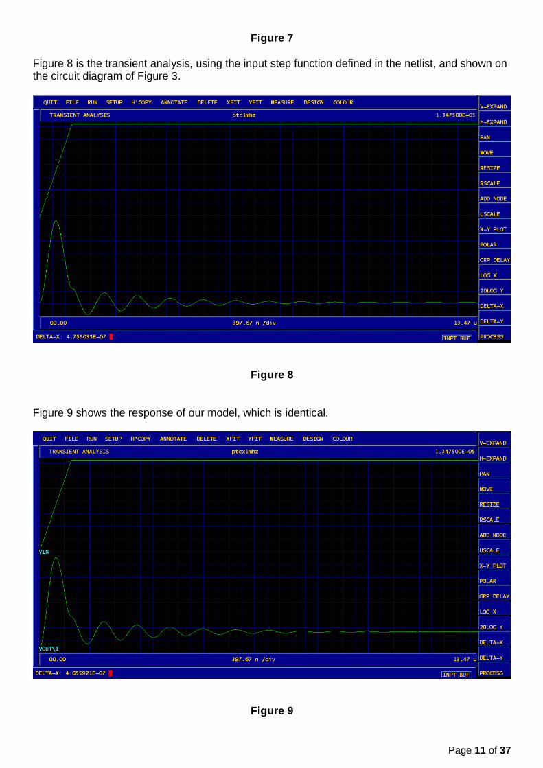
Figure 7 Figure 8 is the transient analysis, using the input step function defined in the netlist, and shown on the circuit diagram of Figure 3.
Figure 8 Figure 9 shows the response of our model, which is identical.
Figure 9

Page 12 of 37
Series Circuit Example
Since there are some differences in the design approach, we also present the design of a 1MHz series resonant circuit, shown in Figure 10.
Figure 10 The components of the tuned circuit are determined from the same assumption that the value of the inductor is 12.665uH. The reader can confirm that the value of the capacitor, derived from the equation:
1 1e6 = ------------------------------- 2.π. sqrt(12.665e-6.C)
is still 2.00002336444e-9 As before, we assume a value of 8.0 for the Q factor, which sets the resonant bandwidth at: 1e6 / 8.0 = 125kHz However, the value of the resistor is now determined from Q = 1/R * sqrt(L/C) R = sqrt(12.665e-6 / 2.00002336444e-9) / 8.0
= 79.5765419 / 8.0 = 9.947068 ohms.
Transfer Function Coefficients
The transfer function of a series resonant circuit is the dual of that of the parallel circuit, given by:

Page 13 of 37
sC H(s) = ---------------------- LCs2 + RCs + 1
Inserting our values gives:
2.00002336444e-9s H(s) = --------------------------------------------------------
2.53302533e-14s2 + 1.98943e-8s + 1 Now we create our SPICE model. Divide top and bottom by s2:
2.00002336444e-9s -1 HH(s) = -----------------------------------------------------------
2.53302533e-14 + 1.98943e-8s-1 + 1s-2 From which we can extract our model parameters: VB1 = 2.0e-9 VA1 = 1.98943e-8 VA2 = 1.0 Note that the only difference between the parallel and series transfer functions is in the numerator. This means that the roots of the denominator will be the same: root 1 = 5.87820740e+06 1/s = 1.7011989e-7 root 2 = -6.66360606e+06 1/s = 1.50068895e-7 The integrator gain is, again, (2 * Q) and the series resistor is 1k, so the values of the capacitors are again 2.722nF and 2.401nF. The values of VB1, VA1, VA2, 2Q, C1 and C2 are added to our Second Order Transfer Function model, earlier shown in Figure 5, and shown updated in Figure 11 below.
Figure 11 SPICE simulations were performed, as with the parallel circuit, but plotting circuit current, instead of voltage. The netlist is included in Appendix 2, and the AC analysis plot is shown in Figure 11, below.

Page 14 of 37
AC Analysis of actual circuit
Figure 12
AC Analysis of Transfer Function
Figure 13

Page 15 of 37
Transient analysis of actual circuit:
Figure 14
Transient Analysis of Transfer Function
Figure 15
As may be seen, the results show excellent correspondence.

Page 16 of 37
Third Order Systems
Figure 16 Although this is not a paper about filter design, we’ll design a simple third order Chebyshev Type I filter, just to illustrate how the modelling procedure follows on from the formal design procedure. We chose this approach, rather than attempt an electrical analogue of a mechanical system firstly, because the characteristic shape of the curve is easily recognisable, so any imperfections in the model are immediately obvious. Secondly and, far more importantly, because we could quickly design a filter to any specification with some code that we wrote to generate test cases. Figure 16 shows the normalised characteristic of a filter with 3dB of passband ripple and 50dB of stopband attenuation. By way of a brief reminder, the frequency at which the response is down 3dB, after the final peak, is the passband edge, while the frequency at which the response is down 50dB is known as the stopband edge. Filters such as the Butterworth, Chebyshev, Elliptical and so on, are designed back-to-front, in that we start with the transfer function, then convert it to real-world components. Also, the design procedure usually produces a so-called ‘normalised’ model, where ωp, the passband edge frequency is set to unity. We will follow such a procedure. The specification for our filter is as follows: Passband, ωp = 1.0 Stopband, ωr = 5.0 Passband ripple, Ap at ωp = 1dB Stopband attenuation, Ar at ωr = 45dB The generic transfer function for a high order system is given by:
-s1.-s2.-s3... H(s) = -------------------------- * K (s-s1)(s-s2)(s-s3)...

Page 17 of 37
where K = 1 for an odd-order filter, and (1 / sqrt(1 + epsilon2)) for even order. We find the poles, s1, s2, s3 as follows: epsilon, which relates to the passband edge = sqrt(100.1Ap - 1) = sqrt(100.1 - 1) = 0.5088471399 lambda, which relates to the stopband edge = sqrt(100.1Ar - 1) = sqrt(104.5 - 1) = 177.825129 We could assume that the order N = 3 but let’s do it the hard way: Some factor, k = ωp/ωr = 1.0 / 5 = 0.2 Some factor, d = epsilon / lambda = 0.5088471399 / 177.825 = 2.8615e-3 1/d = 349.466697 1/k = 5.0 acosh(1/d) = 6.5495 acosh(1/k) = 2.29243 Filter order, N = acosh(1/d) / acosh(1/k) = 2.857, so we’ll say N = 3, and accept the improvement in passband ripple. Some factor, y = 1/N(asinh(1/epsilon) = 1/3(asinh(1/0.5088471399)) sinh(y) = (ey - e-y)/2 = 0.4941706 cosh(y) = (ey + e-y)/2 = 1.1154383 Now we can use these two values to calculate the locations of the interesting poles, all of which lie in the left-hand s-plane. Note that this next operation calculates s = (sigma + jω). s1 = -sin(π/6) * 0.4941706 + jcos(π/6) * 1.1154383 = -2.47085302e-01 + j9.65998675e-01 s2 = -sin(π/2) * 0.4941706 + jcos(π/2) * 1.1154383 = -4.94170605e-01 + j0 s3 = -sin(π/6) * 0.4941706 + jcos(5π/6) * 1.1154383 = -2.47085302e-01 - j9.65998675e-01 3dB bandwidth = 1/N(cosh-1(1/epsilon)) = (1.296644 / 3) = 0.43221 Truncating the ugly numbers: s1 = -0.2471 + j0.9660 s2 = -0.4942 + j0 s3 = -0.2471 - j0.9660 We spare the reader the pages of boring multiplications in the numerator and denominator (which were done by a computer program, anyway), and substitute the results in our generic transfer function to give: -0.4913 H(s) = -------------------------------------------- s3 + 0.9883s2 + 1.2384s + 0.4913 Divide t&b by s3 to get our model parameters: -0.4913s-3 H(s) = -------------------------------------------- 1 + 0.9883s-1 + 1.2384s-2 + 0.4913s-3 VB3 = -0.4913 VA1 = 0.9883

Page 18 of 37
VA2 = 1.2384 VA3 = 0.4913 Note! The polarity of VB3 sets the time-domain polarity of the output. Figure 16, below, shows how we extend our second-order model to a third-order model.
MULTIPLY BY -A1
MULTIPLY BY B0
MULTIPLY BY -B1
INTEGRATE
ADD
ADD
Vin Vout
1/s
INTEGRATE
MULTIPLY BY - B2
MULTIPLY BY -A2
B0
B1 B2
A1
A2
1/s^2
3rd Order Laplace Transfer Function
INTEGRATE
MULTIPLY BY -B3
B3
MULTIPLY BY -A3
A3
1/s^3
Figure 17
Basically, we add another integrator, whose output is multiplied by any third numerator coefficient, and feeds the output adder. We also add another denominator feedback element whose output, after multiplication by a third coefficient, feeds the input adder. The corresponding SPICE model now becomes that of Figure 18.
Figure 18

Page 19 of 37
Integrator Considerations
As before, we need to set up the integrators to reflect the correct frequency range, and it should be noted that we have set the polarity of the second integrator to a negative value, since we have one real root, and two complex conjugate roots. If we had set the first and third integrators negative, and left the second positive, the AC analysis would look the same, but the time-domain response would be unstable and oscillatory. If we failed to set any of the integrators negative, the AC analysis would be distorted, and would resemble a Butterworth response. Previously, with second-order systems, we found that the time-constant and gain of the integrator affected the centre frequency and bandwidth of the system. This is not the case with normalised third order systems. We designed our filter for ωp = 1 radian/second, corresponding to a frequency of 1/2π, whose period is 2π, (6.2831853), and which sets the time-constant of our integrator, which sets the centre frequency of our simulation. To keep the numbers simple, we can set the integrator’s resistor to 1e6, and its gain to 1e6, so that 1/2π = CR/A so C = A / (2π * R) = 1/2π Since A = R, we can fix the values of all three components for any Chebyshev filter. When we run the model in the simulator, the only difference in the shape of the curve, will be the amplitude of the passband ripple, and the gradient of the rolloff to the stopband edge.
Denormalisation
Usually, the next step in a filter design is to ‘denormalise’ the transfer function, by replacing ‘s’ with ‘s/2π.f’, to facilitate manual plotting of the frequency response. The denormalised transfer function is unsuitable for simulation, since the values of ‘f’ cannot be swept by SPICE.
Simulation Results
An AC analysis was performed, to check that the -1dB point was at a frequency of 1rad/sec 0.159154943 Hz), and that the response was -45dB at a frequency of 5rad/sec (0.7957747 Hz)
Figure 19

Page 20 of 37
Viewing the same results on a log y-axis results in the following:
Figure 20 Making accurate measurements was difficult, so we dumped the curve to an ASCII file, and ran it through some analysis code. In actual fact, the stopband edge was at 4.49 rad/sec (0.715 Hz), the improvement being due to our rounding up of the value of ‘N’ from 2.857 to 3, when we designed the filter.
Figure 21 Figure 21 shows the filter’s response to a 1v step input, and the netlist of the model is included in Appendix 3

Page 21 of 37
Modelling Control Systems
X(s) G(s) H(s)
Hfb(s)
E(s)Y(s)
Y(s)
Figure 22
It is assumed that the reader knows that PID stands for ‘Proportional, Integral, Differential’, and what the purpose of this device is. A PID-controlled system is shown above. Briefly, proportional control is applied via G(s), which basically comprises an error amplifier, while Hfb(s) has the characteristic of an integrator, a differentiator, or both. The system is a closed-loop feedback system, whose output parameter is governed by the classical equation:
X * A Y = ----------- 1 - AB
Where ‘A’ is the forward gain of the system, and ‘B’ is the fraction of the output fed back to the input. For some reason, control systems make the assumption that the feedback is inherently negative, and that the fraction fed back is unity, which means that Hfb(s) is equal to H(s). This gives rise to the definition of the transfer function of the system shown in Figure 16 as: Y(s) G(s) * H(s) G(s) ----- = ---------------------- = --------------------- X(s) 1 + (G(s) * H(s)) (1/H(s)) + G(s) This latter form replaces two multiplication operations with one division, and which, in the interests of simpler algebra, is the form we shall use. G(s) can have the values Kp (proportional control), sKd (derivative control), Ki/s (integral control) or any combination of these. We will apply our PID controls to a fictitious system, H(s), comprising a simple DC servo motor, with little regard for the ‘correct’ design procedure of a control system. Our only intent is to exaggerate the effect of each control to make its operation easy to understand. However, readers are encouraged to replace our arbitrary values with their own, to simulate a real-world system. We will need a second-order model to simulate the open-loop, proportional and differential controls, and a third-order model for the integral and full-PID controls. The schematics for both models may be found in Appendix 5. Since our simulation models need a value of ‘Q’ in order to work accurately, we will arbitrarily choose a value of 8, whether or not this is even remotely applicable to a real process.

Page 22 of 37
Open Loop Response
The angular velocity of a servo motor and its load may be defined as: (k / JL) * X(s) Y(s) = ----------------------------------------------------- s2 + ((B / J) + (R / L))s + ((RB + k2) / JL) Where Y(s) is the output parameter (in this case, angular velocity), X(s) is an input parameter, such as supply voltage, k is a constant relating input current to output torque, and R and L are the resistance and inductance of the armature. J and B have their traditional meanings, as armature moment of inertia and coefficient of friction. From the above, the Laplace transfer function becomes: Y(s) (k / JL) ------ = ----------------------------------------------------- X(s) s2 + ((B / J) + (R / L))s + ((RB + k2) / JL) We purchased an unremarkable DC servo motor, and entered its values into this equation to give the transfer function: (0.05 / (0.01 * 50e-3)) H(s) = ---------------------------------------------------------------------------------------------------- s2 + ((1.719e-2/0.01) + (20/50e-3))s + ((20*1.719e-2)+0.025)) /( 0.01*50e-3) which reduced to:
100 H(s) = --------------------------- s2 + 401.8s + 737.6
We determine the roots of the denominator, which are calculated to be: s1 = -1.84420380e+00 s2 = -3.99955796e+02 1/s1 = 0.54223942 1/s2 = 2.5002763e-3 We use these to calculate the parameters of our second-order model’s two integrators. We use a ‘Q’ value of 8, since we have no idea what the actual value for such a motor, together with its inertial load, should be: The integrator gain is: A = 2Q = 16, and the integration resistor R = 1e3 C = (1/s) * A / 1e3 C1 = 0.54223942 * 16 / 1e3 = 8.67583072e-3 C2 = 2.5002763e-3 * 16 / 1e3 = 4.00044208e-5 Normalising the transfer function for use in the simulation model: 100s-2 HH(s) = ------------------------------ 1+ 401.8s-1 + 737.6s-2 The model coefficients are B2 = 100, A1 = 401.8, A2 = 737.6, which we plug into our generic second-order model, shown in Appendix 5.

Page 23 of 37
As mentioned earlier in this paper, in addition to integrating, the integrators in our model attenuate the signal, so we need to correct this by applying a normalised scaling factor for the output variable, Vout. Ordinarily, we would use (s2 / R) where s2 is the second root of the denominator, and R is the integration resistance, which would yield a factor of (-3.99955796e+02 / 1e3) = -0.399955796. However, this is a motor, so we might want to express the angular velocity in revolutions per minute, radians per second, or Hertz, meaning that we can set the scaling factor to anything meaningful. Applying the scaling factor derived above gives an output of 105mV for a 20v input, but we would like to see about 1v out for 1v in, so we multiply it by 20, to give 7.99911592. Now an output of 20v corresponds to the top speed of 1200rpm, and a 1volt output is equivalent to 60rpm, or 1 revolution per second. Performing an AC analysis gave us the motor’s frequency response, shown in Figure 24 below. However, it should be noted that this is actually a measure of how the inertia affects the motor’s ability to adjust its speed in response to an input signal. It may be seen that very fast rates of change of voltage result in very slight changes in angular velocity. The magnitude is shown on a linear scale, since measuring it in dB is totally meaningless.
Figure 23 Next, we ran another AC analysis and plotted real and imaginary values of the output parameter, a polar plot of which is shown in Figure 23a.

Page 24 of 37
Figure 23a
The transient response of the motor speed to a step of input voltage, simulating the switch-on condition, is shown in Figure 24. It may be seen that the delay time from switch-on to the peak of the overshoot (which is a more convenient measurement point than the 90% value) is approximately 5ms.
Figure 24

Page 25 of 37
Proportional control (Kp=100)
Proportional control applies a correction based on the difference between required speed and current speed. Increasing the proportional gain has the effect of proportionally increasing the control signal for the same level of error, such that the closed-loop system reacts more quickly, but tends to overshoot under certain conditions. The proportional gain factor, Kp, is the change in output for a unity change of input. We set Kp to 100.
C(s)H(s) C(s)H(s) C(s) Closed loop transfer function = ----------------- = ------------------- = ------------------
1 + C(s)Hfb(s) 1 + C(s)H(s) 1/H(s) + C(s) 100 H(s) = --------------------------- 1/H(s) = 1e-2(s2 + 401.8s + 737.6) = 1e-2s2 + 4.018s + 7.376 s2 + 401.8s + 737.6 100 Closed loop = ------------------------------------------ 1e-2s2 + 4.018s + 7.376 + 100 100 H(s) = ----------------------------------- 1e-2s2 + 4.018s + 107.376 S1 = -2.87860552e+01 S2 = -3.73013945e+02 1/s1= 3.473904e-2 1/s2= 2.68086492e-3 C1 = 0.03473904 * 16 /1e3 = 5.5582464e-4 C2 = 2.68086492e-3 * 0.016 = 4.28938387e-5 100s-2 HH(s) = ------------------------------------- 1e-2 + 4.018s-1 + 107.376s-2
b2=100,a1=4.018,a2=107.376,c1=5.5582464e-4,c2=4.28938387e-5 Since Kp is 100, the overall gain has increased, so we change our output scaling factor from 7.99911592 to 0.799911592. The step response is now as shown in Figure 25, and clearly shows that the rise time has decreased, from 5ms to 3ms. The output oscillates about the nominal value, since the apparent error voltage is now 100 times greater, causing the correction to overshoot and undershoot wildly:

Page 26 of 37
Figure 25
Proportional + Differential control – Kp=100, Kd=10s
Differential feedback slows the rise time, and increases the overshoot/undershoot, because it anticipates the next change in the input/control signal. If the slope of the error is positive, the control signal, which is now proportional to the slope, can become large, even while the magnitude of the error is still relatively small. This anticipation can cause the system to overshoot, but if adjusted correctly, can actually reduce overshoot. We make no attempt to optimise this, but merely to point out that we have exaggerated the effect. Kp=100, Kd=10s C(s) = Kp + Kd = (100 + 10s) 100 H(s) = -------------------------- 1/H(s) = 1e-2(s2 + 401.8s + 737.6) = 1e-2s2 + 4.018s + 7.376 s2 + 401.8s + 737.6
C(s) 10s + 100 Closed loop TF = ----------------- = -------------------------------------------------
1/H(s) + C(s) 1e-2s2 + 4.018s + 7.376 + 100 + 10s 10s + 100 H(s) = -------------------------------------- 1e-2s2 + 14.018s + 107.376 S1 = -7.70218552e+00 S2 = -1.39409781e+03 1/s1 = 0.1298332788 1/s2 = 7.1730978474e-4 C1 = 2.0773324608e-3 C2 = 1.147695655584e-5

Page 27 of 37
10s-1 + 100s-2 HH(s) = -------------------------------------- 1e-2 + 14.018s-1 + 107.376s-2
b1=10,b2=100,a1=14.018,a2=107.376,c1=2.0773324608e-3,c2=1.147695655584e-5
Figure 26
Proportional + Integral Control
By adding an integral term to the controller we hope to reduce steady-state error. The integrator creates a running sum of the error, thereby continually increasing the control signal which in turn tries to reduce the error. However, the overall effect of the integration is that the response time of the system is increased, and there may be a tendency towards low-frequency oscillatory operation. The integration only stops when the error signal changes sign, so an excessively long integration time constant may lead to what is known as integration windup. It may be worth mentioning that as Ki decreases, the integration time constant increases.
Proportional + Integral Kp=70 Ki=5/s
C(s) = KP + Ki/s = (70 + 5/s)
C(s)H(s) C(s)H(s) C(s) Closed loop transfer function = ----------------- = ------------------- = ------------------
1 + C(s)Hfb(s) 1 + C(s)H(s) 1/H(s) + C(s) 100 H(s) = -------------------------- 1/H(s) = 1e-2(s2 + 401.8s + 737.6) = 1e-2s2 + 4.018s + 7.376
s2 + 401.8s + 737.6

Page 28 of 37
(Kp + Ki/s) Hcl(s) = ----------------------------------- 1e-2s2 + 4.018s + 7.376 + Kp + Ki/s Multiply T&B by s: Kps + Ki H(s) = -------------------------------------------------- 1e-2s3 + 4.018s2 + 7.376s + Kps + Ki 70s + 5 H(s) = -------------------------------------------------- 1e-2s3 + 4.018s2 + 7.376s + 70s + 5
70s + 5 H(s) = ------------------------------------------ 1e-2s
3 + 4.018s
2 + 77.376s + 5
70s-2 + 5s-3
HH(s) = -------------------------------------------- 1e-2 + 4.018s-1 + 77.376s2 + 5s-3
s1 = -3.81513076e+02 s2 = -2.02111681e+01 s3 = -5.42014808e-02 1/s1 = 2.6211421387821580196637873560066e-3 1/s2 = 4.9477595508198261930244397898012e-2 1/s3 = 18.44968043751306514120182487708 c1 = 4.193827422e-5 c2 = 7.9164152813e-4 c3 = 0.295194887 b2=70,b3=5,a1=4.018,a2=77.376,a3=5,c1=4.193827422e-5,c2=7.9164152813e-4,c3=0.295194887 This is a third-order system, so we now need to apply the above coefficients to our third-order model, whose schematic is also shown in Appendix 5.

Page 29 of 37
Figure 27 As may be seen, integral control averages changes in the control signal, over a period set by the Ki parameter. This delays reaching the steady state, but does so smoothly, without overshoot.
Page 30 of 37
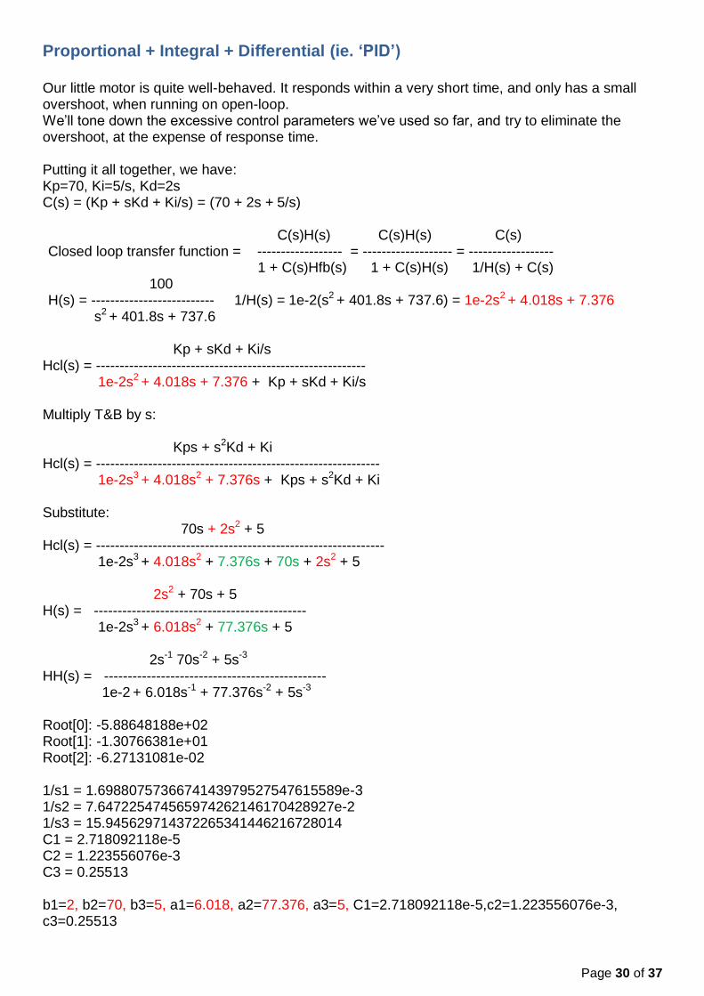
Proportional + Integral + Differential (ie. ‘PID’)
Our little motor is quite well-behaved. It responds within a very short time, and only has a small overshoot, when running on open-loop. We’ll tone down the excessive control parameters we’ve used so far, and try to eliminate the overshoot, at the expense of response time. Putting it all together, we have: Kp=70, Ki=5/s, Kd=2s C(s) = (Kp + sKd + Ki/s) = (70 + 2s + 5/s)
C(s)H(s) C(s)H(s) C(s) Closed loop transfer function = ------------------ = ------------------- = ------------------
1 + C(s)Hfb(s) 1 + C(s)H(s) 1/H(s) + C(s) 100 H(s) = -------------------------- 1/H(s) = 1e-2(s2 + 401.8s + 737.6) = 1e-2s2 + 4.018s + 7.376
s2 + 401.8s + 737.6 Kp + sKd + Ki/s Hcl(s) = --------------------------------------------------------- 1e-2s2 + 4.018s + 7.376 + Kp + sKd + Ki/s Multiply T&B by s: Kps + s2Kd + Ki Hcl(s) = ------------------------------------------------------------ 1e-2s3 + 4.018s2 + 7.376s + Kps + s2Kd + Ki Substitute: 70s + 2s2 + 5 Hcl(s) = ------------------------------------------------------------- 1e-2s3 + 4.018s2 + 7.376s + 70s + 2s2 + 5 2s2 + 70s + 5 H(s) = --------------------------------------------- 1e-2s3 + 6.018s2 + 77.376s + 5 2s-1 70s-2 + 5s-3 HH(s) = ----------------------------------------------- 1e-2 + 6.018s-1 + 77.376s-2 + 5s-3
Root[0]: -5.88648188e+02 Root[1]: -1.30766381e+01 Root[2]: -6.27131081e-02 1/s1 = 1.6988075736674143979527547615589e-3 1/s2 = 7.647225474565974262146170428927e-2 1/s3 = 15.945629714372265341446216728014 C1 = 2.718092118e-5 C2 = 1.223556076e-3 C3 = 0.25513 b1=2, b2=70, b3=5, a1=6.018, a2=77.376, a3=5, C1=2.718092118e-5,c2=1.223556076e-3, c3=0.25513
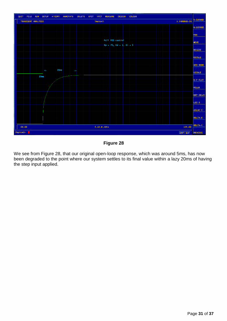
Page 31 of 37
Figure 28 We see from Figure 28, that our original open-loop response, which was around 5ms, has now been degraded to the point where our system settles to its final value within a lazy 20ms of having the step input applied.

Page 32 of 37
Follow-up
Readers are encouraged to redesign the control system and improve on these results,
Ongoing Research
The scaling factor derived so far for the second-order model output voltage varies with the topology of the circuit, which is very inconvenient. Research continues in an attempt to find a common approach
Cascading transfer function models to represent complex systems
Z-plane transfer function simulation with SPICE

Page 33 of 37
Appendix 1
Netlist of parallel resonant circuit of Figure 3
ptc1mhz *.ac dec 5000 100k 10meg *.print ac v(2) .tran 50n 15u 0 50n .print tran v(3) v(2) *#iplot all *#run *#quit l1 2 0 12.665u c1 2 0 2e-9 r1 3 2 636.612 v1 3 0 pwl 0 0 1e-6 5 dc 0 ac 5 .end
Netlist of second order transfer function model of Figure 5
ptc1mhzx .ac dec 10000 100k 10meg .print ac v(2) *.tran 50n 15u 0 50n *.print tran v(11) v(2) *#iplot all *#run *#quit r1 2 0 1g r2 4 0 1g b1 4 11 v=(v(9)*v(3)) + (v(10)*v(8)) c1 3 0 2.722nf r3 6 0 1g b2 2 0 v=-1.0467282e4*((v(5)*v(4)) + (v(7)*v(3)) + (v(6)*v(8))) c2 8 0 2.401nf vb2 6 0 0.0 v2 11 0 pwl 0 0 1e-6 5 dc 0 ac 5 vb1 7 0 12.665e-6 vb0 5 0 0 va2 10 0 1.0 va1 9 0 1.989425336e-8 e1 12 0 4 0 -1.60e1 e2 13 0 3 0 1.60e1 r4 12 3 1.0e3 r5 13 8 1.0e3 r6 5 0 1g r7 7 0 1g r8 9 0 1g r9 10 0 1g .end

Page 34 of 37
Appendix 2
Netlist of series resonant circuit of Figure 10
rlc1mhz .ac dec 10000 100k 10meg .print ac i(v1) *.tran 50n 20u 0 50n *.print tran i(v1) *#iplot all *#run *#quit r1 1 2 9.947068 l 2 3 12.665u c1 3 0 2.00e-9 v1 1 0 pwl 0 0 1e-6 0 2e-6 5 dc 0 ac 5 .end
Netlist of second order transfer function model of Figure 11
rlc1mhzx .ac dec 10000 100k 10meg .print ac v(2) *.tran 50n 20u 0 50n *.print tran v(11) v(2) *#iplot all *#run *#quit r1 2 0 1g r2 4 0 1g b1 4 11 v=(v(9)*v(3))+(v(10)*v(8)) c1 3 0 2.722n r3 6 0 1g b2 2 0 v=6.6636e6*((v(5)*v(4)) + (v(7)*v(3)) + (v(6)*v(8))) c2 8 0 2.401n v1 6 0 dc 0.0 v2 11 0 pwl 0 0 1e-6 0 2e-6 5 1 dc 0 ac 5 v3 7 0 2.000023e-9 v4 5 0 dc 0 v5 10 0 1.0 v6 9 0 1.98943e-8 e1 12 0 4 0 -16.0 r4 12 3 1e3 e2 13 0 3 0 16.0 r5 13 8 1e3 r6 5 0 1g r7 7 0 1g r8 9 0 1g r9 10 0 1g .end

Page 35 of 37
Appendix 3
Netlist of Chebyshev filter model
chtest1b ** Chebyshev filter: wp=1 wr=5wp ap=1 ar=45 *.ac dec 10000 10m 10 *.print ac v(2) .tran 100u 5.0 0 100u .print tran v(6) v(2) *#iplot all *#run *#quit r1 2 0 1g r2 4 0 1g b1 4 6 v=(v(12)*v(3)) + (v(10)*v(8)) + (v(9)*v(11)) b2 2 0 v=1.0*((v(14)*v(4)) + (v(13)*v(3)) + (v(7)*v(8)) + (v(5)*v(11))) c1 3 0 1.5924E-01 c2 8 0 1.5924E-01 c3 11 0 1.5924E-01 r3 15 3 1e6 r4 17 8 1e6 r5 16 11 1e6 r6 0 12 1g r7 13 0 1g r8 14 0 1g e1 16 0 8 0 1e6 e2 15 0 4 0 -1e6 e3 17 0 3 0 1e6 r9 0 10 1g r10 0 9 1g r11 7 0 1g r12 5 0 1g vb3 5 0 -0.4913 vb2 7 0 0.0 vb1 13 0 0.0 vb0 14 0 0.0 va1 12 0 0.9883 va2 10 0 1.2384 va3 9 0 0.4913 v8 6 0 pwl 0 0 1e-6 0 2e-6 1 ac 1 .end

Page 36 of 37
Appendix 4
Hypothetical Transfer Function Frequency Domain
Hypothetical Transfer Function Time Domain

Page 37 of 37
Appendix 5