lan & wan clock generation and muxing using the cdce62005
TRANSCRIPT
Application ReportSCAA098–November 2008
LAN and WAN Clock Generation and Muxing Using theCDCE62005
Firoj Kabir / Johnny Lau................................................................................... Clock Distribution Circuits
ABSTRACTThis application note is a guide for using Texas Instruments CDCE62005 in aLAN/WAN application as a clock distributor and clock synthesizer along with measuredjitter performance results. In addition, several examples are given to show the flexibilityof the CDCE62005 generating the most common frequencies used in variousnetworking applications today.
Contents1 Background.......................................................................................... 22 Functional Description ............................................................................. 23 Application ........................................................................................... 34 Test Equipment, Setup, and Measured Results ................................................ 45 Test Equipment and Setup ........................................................................ 6
5.1 Configuration #1 Phase Noise Plot Results............................................ 75.2 Configuration #2 Phase Noise Plot Results .......................................... 135.3 Configuration #3 Phase Noise Plot Results .......................................... 205.4 Configuration #4 Phase Noise Plot Results .......................................... 25
6 Performance Summary........................................................................... 306.1 Configuration #1.......................................................................... 306.2 Configuration #2.......................................................................... 306.3 Configuration #3.......................................................................... 306.4 Configuration #4.......................................................................... 31
7 Conclusion ......................................................................................... 31
List of Figures
1 CDCE62005 Functional Block Diagram ......................................................... 32 Setup Configuration # 1............................................................................ 43 Setup Configuration # 2............................................................................ 44 Setup Configuration # 3............................................................................ 55 Setup Configuration # 4............................................................................ 56 Setup Configuration # 1............................................................................ 67 TI GUI Setup Configuration # 1................................................................... 68 Setup Configuration # 2 .......................................................................... 129 TI GUI Setup Configuration # 2 ................................................................. 1210 Setup Configuration # 3 .......................................................................... 1811 TI GUI Setup Configuration # 3 – CDCE62005 #1 ........................................... 1812 TI GUI Setup Configuration # 3 – CDCE62005 #2 ........................................... 1913 Setup Configuration # 4 .......................................................................... 2414 TI GUI Setup Configuration # 4 ................................................................. 24
SCAA098–November 2008 LAN and WAN Clock Generation and Muxing Using the CDCE62005 1Submit Documentation Feedback
1 Background
2 Functional Description
Background www.ti.com
Networking equipment frequently has a need for clock muxing different frequencies to meet a givensystem application. Traditional methods involved 2 different clock oscillators and a clock mux device. ForLAN applications, a typical 156.25 MHz clock is needed, and for WAN applications a 155.52 MHz clock isused. Due to the low jitter and accuracy needed for these clock oscillators, the cost of these oscillatorsmay be high. To obtain lower cost but maintain the low jitter, high accuracy, and clock muxing in a singlesolution, the CDCE62005 can be used.
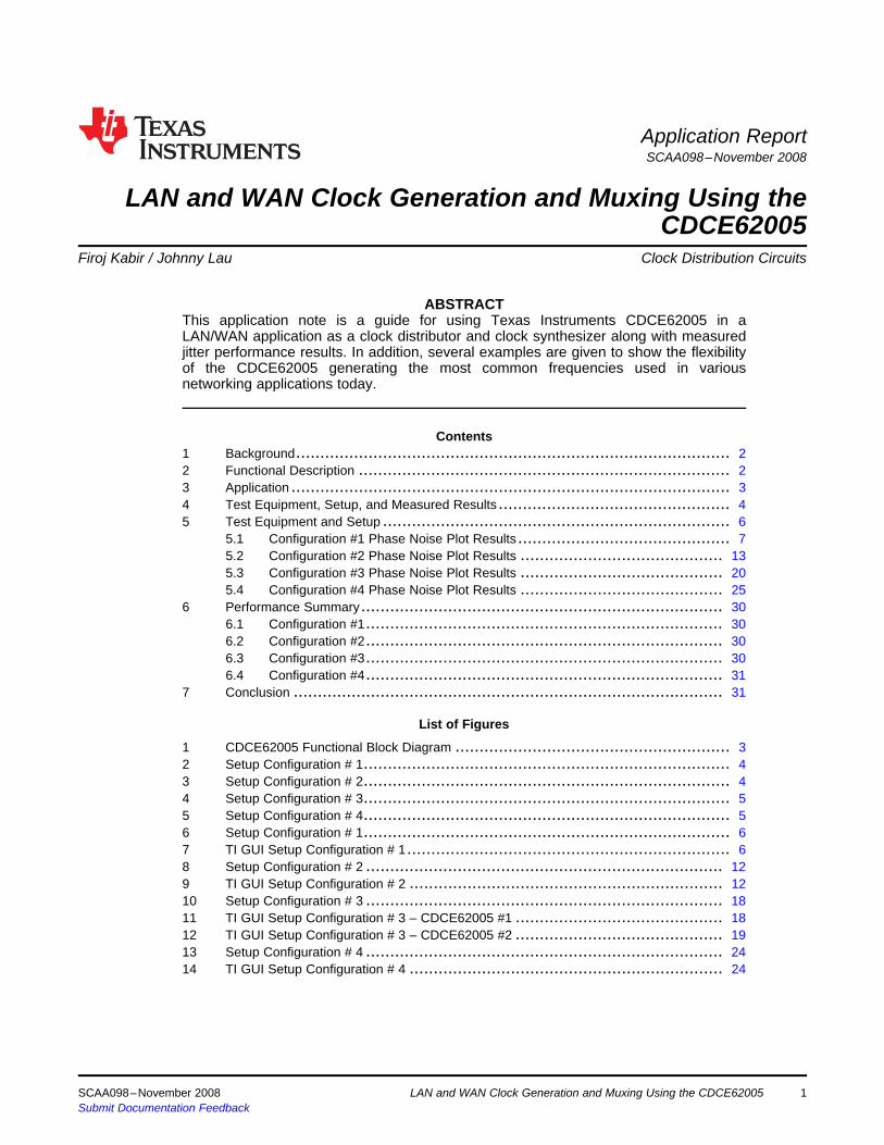
The CDCE62005 is a high performance low phase noise clock synthesizer with five universal outputbuffers that can be configured individually to be LVPECL, LVDS or LVCMOS. Each of the 5 universaldifferential outputs can be converted to two LVCMOS outputs for a total of 10 LVCMOS outputs. It has twofully integrated low noise LC based Voltage Controlled Oscillators (VCOs) which operates in the 1.750GHz -2.356 GHz range. The VCO Core output frequency is proportional to the frequency of the VCO coreinput, the pre-scaler divider, feedback divider, output divider and VCO selection. Each output has anindependent Output Divider and each output can be sourced from the Primary Input, Secondary Input,Smart Mux Output, or the Output of the Integrated VCO Core. Another unique feature is the output phaseadjust. All device settings are programmable through a SPI serial interface and the CDCE62005 containsan integrated EEPROM to store all user settings for use on power on default settings.
For more details refer to the application note, Using the CDCE62005 as a Frequency Synthesizer ..
2 LAN and WAN Clock Generation and Muxing Using the CDCE62005 SCAA098–November 2008Submit Documentation Feedback
Output
Divider 0
U 0 P
U 0N
Output
Divider 1
U 1 P
U 1N
Output
Divider 2
U 2 P
U 2N
Output
Divider 3
U 3 P
U 3N
Output
Divider 4
U 4 P
U 4N
PFD /
CP
/1:/2:HiZ
/1:/2:HiZ
PrescalerFeedback
Divider
Input
Divider
Reference
Divider
AUX
OUT
PRI _IN
SEC _ IN
XTAL /
AUX _IN
EEPROM
Interface
&
Control
REF_ SELECT
Power _Down
RESET or HOLD
MODE_ SELECT
SPI _ LE
SPI _CLK
SPI _MISO
SPI _MOSI
EXT _LFP
EXT _LFN
3 Application
www.ti.com Application
Figure 1. CDCE62005 Functional Block Diagram
Networking LAN and WAN clocking needs require low jitter (typ < 1ps rms or lower). Typical clock speedsfor LAN applications are 625 MHz, 312.5 MHz, 156.25 MHz, 125 MHz, and 25 MHz. For WAN applications622.08 MHz, 311.04 MHz, 155.52 MHz, 77.76 MHz, and 19.44 MHz are commonly used. For both LANand WAN systems, the output signal type needed can be differential (LVPECL or LVDS) or single ended3.3V LVCMOS. This application report demonstrates 4 solutions that can meet these needs while alsooffering a lower cost solution to oscillators and clock muxes.
SCAA098–November 2008 LAN and WAN Clock Generation and Muxing Using the CDCE62005 3Submit Documentation Feedback
4 Test Equipment, Setup, and Measured Results
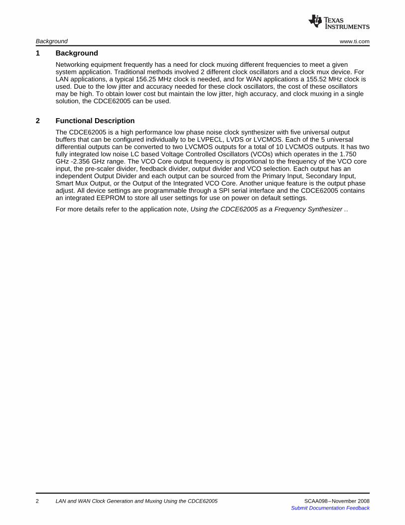
25 MHz
Y0: 125 MHz LVDS
Y1: 3125 MHz LVPECL
Y2: 156.25 MHz LVPECL
Y3: 625 MHZ LVDS
Y4: 2x25 MHZ 3.3 V LVCMOS
Synthesizer
CDCE62005
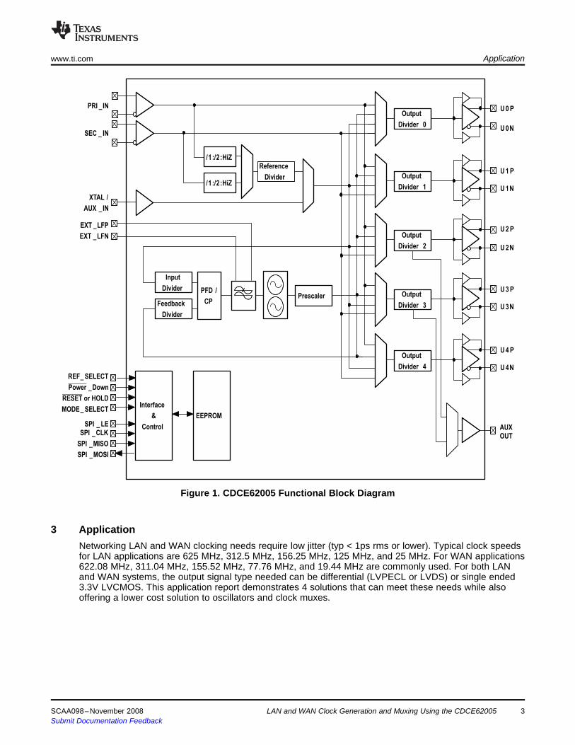
Synthesizer
Y1: 311.04 MHz LVPECL
Y2: 155.52 MHz LVPECL
Y0: 77.76 MHz LVDS
24.8832 MHz
Y3: 2x19.44 MHz 3.3 V LVCMOS
Y4: 622.08 MHz LVPECL
CDCE62005
Test Equipment, Setup, and Measured Results www.ti.com
1. A solution on how to generate networking LAN clocks from a single CDCE62005 device and a low costcrystal is provided in Figure 2.
Figure 2. Setup Configuration # 1
Figure 2 uses a standard 25 MHz crystal connected to the CDCE62005 auxiliary input. The 25 MHz isthen fed into the CDCE62005 VCO core to generate a 625 MHz frequency available to all five outputmuxes. From there post dividers can be used to output 625 MHz, 312.5 MHz, 156.25 MHz, 125 MHz,and 25 MHz. The output signal type can be native LVPECL, LVDS, or LVCMOS; and can be mixed toavoid use of external components to accomplish signal type translation. This example selects all threetypes to show the flexibility of the CDCE62005 output buffers. For every differential output, 2 LVCMOSsignals can take its place as shown. In the above example, the CDCE62005 outputs 4 differentialsignals and 2 LVCMOS signals.
2. Second is a solution on how to generate networking WAN clocks from a single CDCE62005 deviceand a low cost crystal.
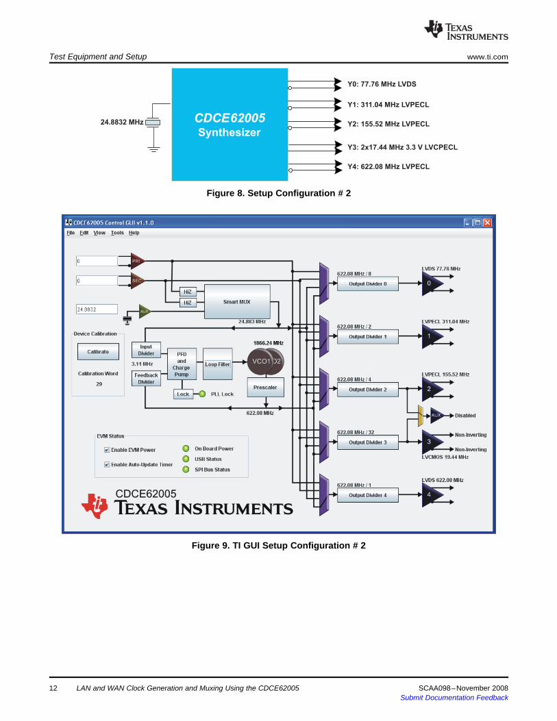
Figure 3. Setup Configuration # 2
Figure 3 uses a standard 24.8832 MHz crystal connected to the CDCE62005 auxiliary input. The24.8832 MHz is then feed into the CDCE62005 VCO core to generate a 622.08 MHz frequencyavailable to all five output muxes. From there post dividers can be used to output 622.08 MHz, 311.04MHz, 155.52 MHz, 77.76 MHz, and 19.44 MHz. The output signal type can be native LVPECL, LVDS,or LVCMOS; and can be mixed to avoid use of external components to accomplish signal typetranslation. Again, this example selects all three types to show the flexibility of the CDCE62005 outputbuffers. It should also be noted that a standard 19.44 MHz crystal can used instead of 24.8832 MHzcrystal to generate above mentioned frequencies.
3. Third is a solution that requires both LAN and WAN clock and that all outputs be frequency selectableusing software to control the output clock muxing. For simplicity, lets limit the frequencies to 156.25MHz and 155.56 MHz that are commonly used in 10G networking designs. It should be noted that anyof the frequencies in example 1 or 2 are also possible if needed.
4 LAN and WAN Clock Generation and Muxing Using the CDCE62005 SCAA098–November 2008Submit Documentation Feedback
CDCE62005
Synthesizer
#2
CDCE62005
Synthesizer
#1
SPI
25 MHz
Y0: 156.25 MHz or 155.52 KHz LVDS
Y1: 153.25 MHz or 155.52 MHz LVPECL
Y2: 156.25 MHz or 155.52 MHz LVPECL
Y3: 156.25 MHz or 155.52 MHz LVDS
24.8832 MHz
U1: 156.25 MHz or 155.52 KHz LVPECL
U2: 153.25 MHz or 155.52 MHz LVPECL
U3: 156.25 MHz or 155.52 MHz LVDS
U4: 156.25 MHz or 155.52 MHz LVPECL
Synthesizer
133.33 MHz LVPECL
1.5 GHz LVPECL
SPI
25 MHz
Y0: 1.5 GHz LVPECL
Y2: 2X125 MHz LVCMOS
Y1: 1.5 GHz LVPECL
Y3: 156.25 MHz LVDS
Y4: 2x133.33 MHz / 66.66 MHz / 33.33 MHz - LVPECL
CDCE62005
www.ti.com Test Equipment, Setup, and Measured Results
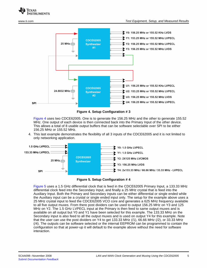
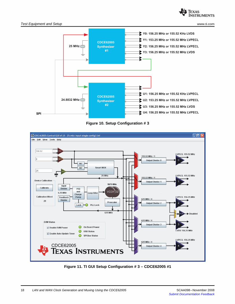
Figure 4. Setup Configuration # 3
Figure 4 uses two CDCE62005. One is to generate the 156.25 MHz and the other to generate 155.52MHz. One output of each device is then connected back into the Primary Input of the other device.This allows a total of 8 usable output buffers that can be software selectable over SPI to be either156.25 MHz or 155.52 MHz.
4. This last example demonstrates the flexibility of all 3 inputs of the CDCE62005 and it is not limited toonly networking application.
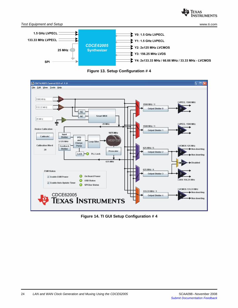
Figure 5. Setup Configuration # 4
Figure 5 uses a 1.5 GHz differential clock that is feed in the CDCE62005 Primary Input, a 133.33 MHzdifferential clock feed into the Secondary Input, and finally a 25 MHz crystal that is feed into theAuxiliary Input. Both the Primary and Secondary inputs can be either differential or single ended whilethe Auxiliary input can be a crystal or single ended input only. The setup for the example above uses a25 MHz crystal input to feed the CDCE62005 VCO core and generates a 625 MHz frequency availableto all five output muxes. From there post dividers can be used to output 156.25 MHz on Y3 and 125MHz on Y2. The 1.5 GHz LVPECL input at the Primary is then feed to same output muxes and isavailable on all output but Y0 and Y1 have been selected for this example. The 133.33 MHz on theSecondary input is also feed to all the output muxes and is used on output Y4 for this example. Notethat the user can use the post dividers on Y4 to get 133.33 MHz (/1), 66.66 MHz (/2), or 33.33 MHz(/4). The outputs can be software selected or the internal EEPROM can be programmed to contain theconfiguration so that at power-up it will default to the example above without the need for softwareinteraction.
SCAA098–November 2008 LAN and WAN Clock Generation and Muxing Using the CDCE62005 5Submit Documentation Feedback
5 Test Equipment and Setup
CDCE62005
Synthesizer25 MHz
Y0: 125 MHz LVDS
Y1: 312.5 MHz LVPECL
Y2: 156.25 MHz LVPECL
Y3: 625 MHz LVDS
Y4: 2x25 MHz 3.3 V LVCMOS
Test Equipment and Setup www.ti.com
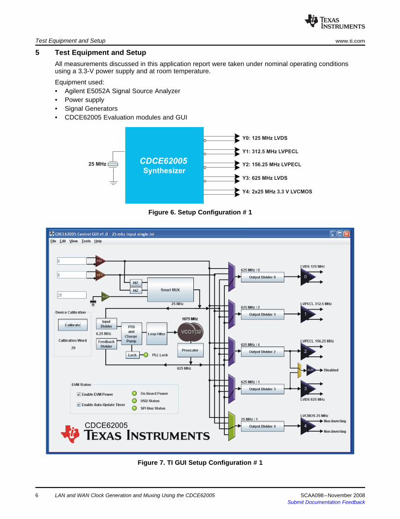
All measurements discussed in this application report were taken under nominal operating conditionsusing a 3.3-V power supply and at room temperature.
Equipment used:• Agilent E5052A Signal Source Analyzer• Power supply• Signal Generators• CDCE62005 Evaluation modules and GUI
Figure 6. Setup Configuration # 1
Figure 7. TI GUI Setup Configuration # 1
LAN and WAN Clock Generation and Muxing Using the CDCE620056 SCAA098–November 2008Submit Documentation Feedback
5.1 Configuration #1 Phase Noise Plot Results
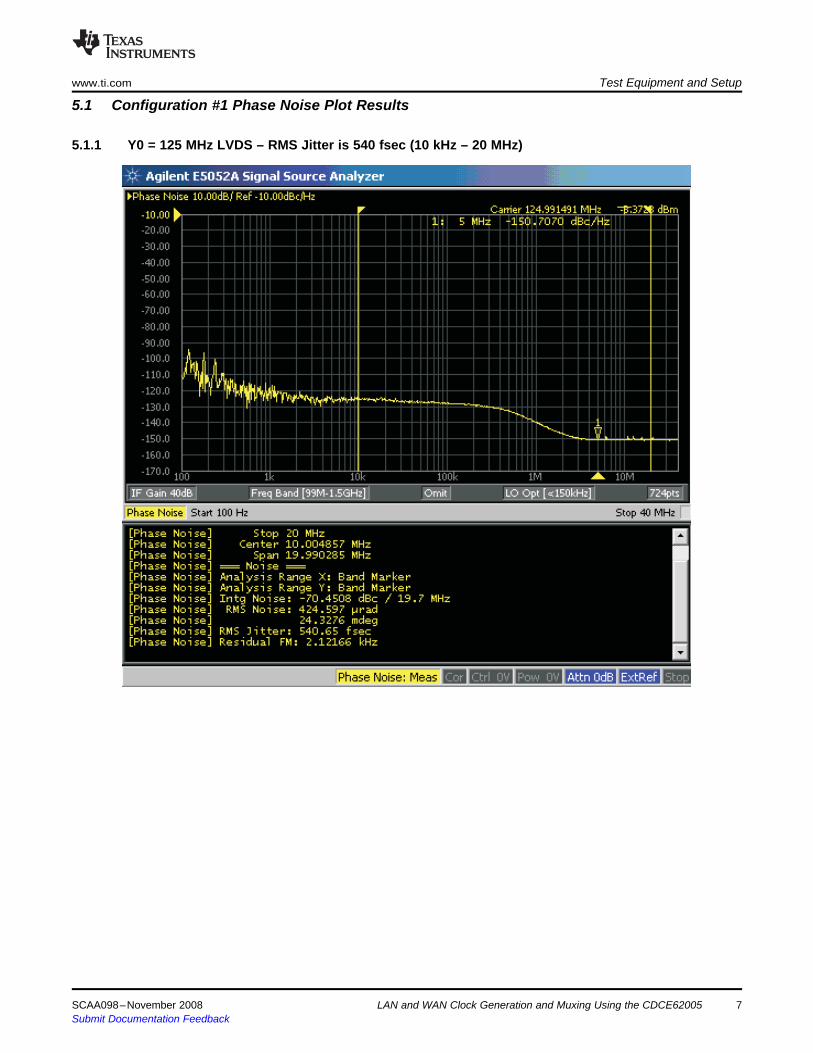
5.1.1 Y0 = 125 MHz LVDS – RMS Jitter is 540 fsec (10 kHz – 20 MHz)
www.ti.com Test Equipment and Setup
SCAA098–November 2008 LAN and WAN Clock Generation and Muxing Using the CDCE62005 7Submit Documentation Feedback
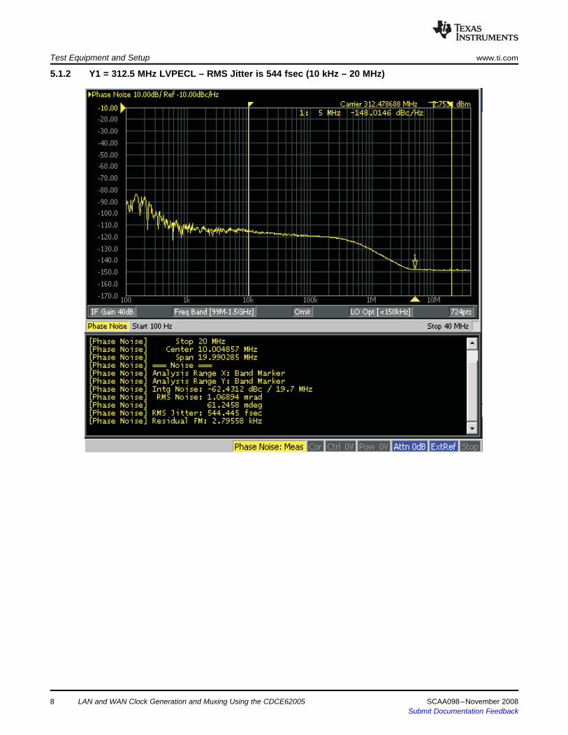
5.1.2 Y1 = 312.5 MHz LVPECL – RMS Jitter is 544 fsec (10 kHz – 20 MHz)
Test Equipment and Setup www.ti.com
LAN and WAN Clock Generation and Muxing Using the CDCE620058 SCAA098–November 2008Submit Documentation Feedback
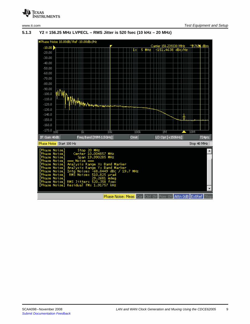
5.1.3 Y2 = 156.25 MHz LVPECL – RMS Jitter is 520 fsec (10 kHz – 20 MHz)
www.ti.com Test Equipment and Setup
SCAA098–November 2008 LAN and WAN Clock Generation and Muxing Using the CDCE62005 9Submit Documentation Feedback
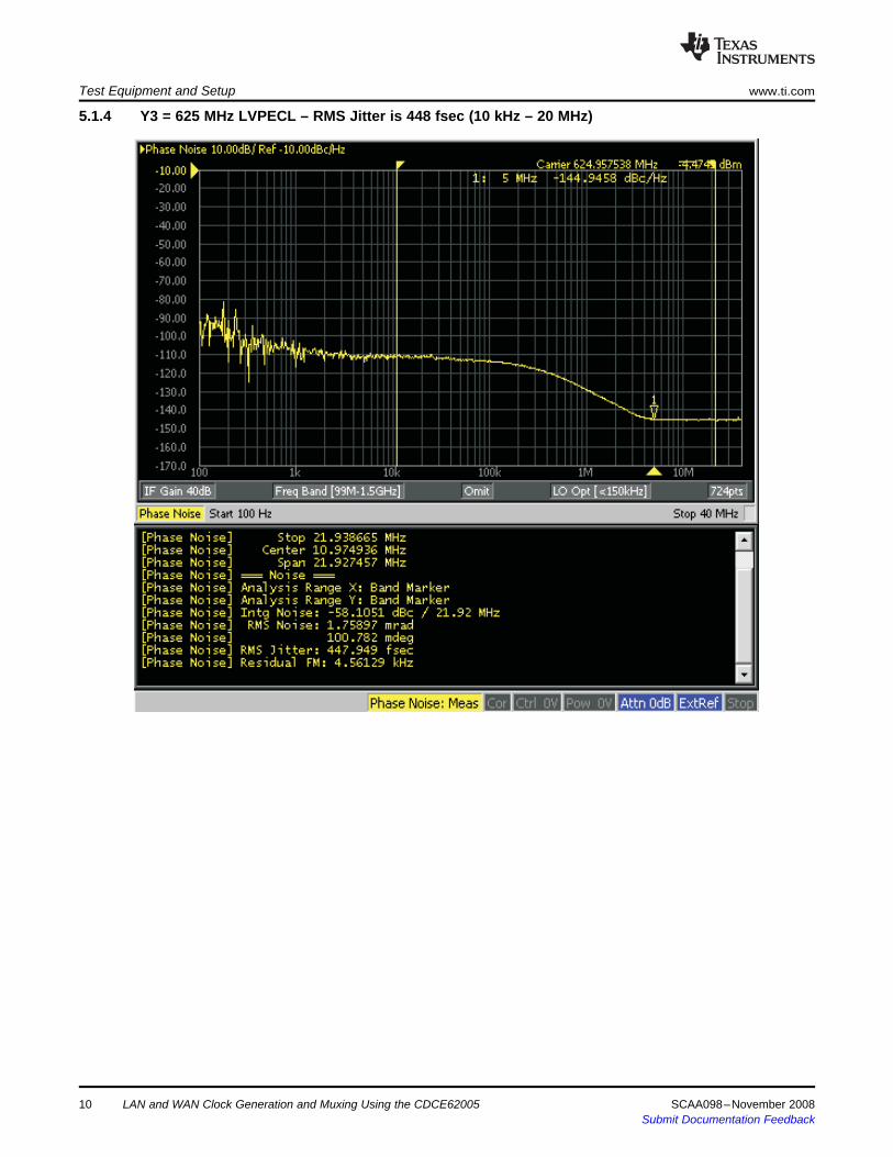
5.1.4 Y3 = 625 MHz LVPECL – RMS Jitter is 448 fsec (10 kHz – 20 MHz)
Test Equipment and Setup www.ti.com
LAN and WAN Clock Generation and Muxing Using the CDCE6200510 SCAA098–November 2008Submit Documentation Feedback
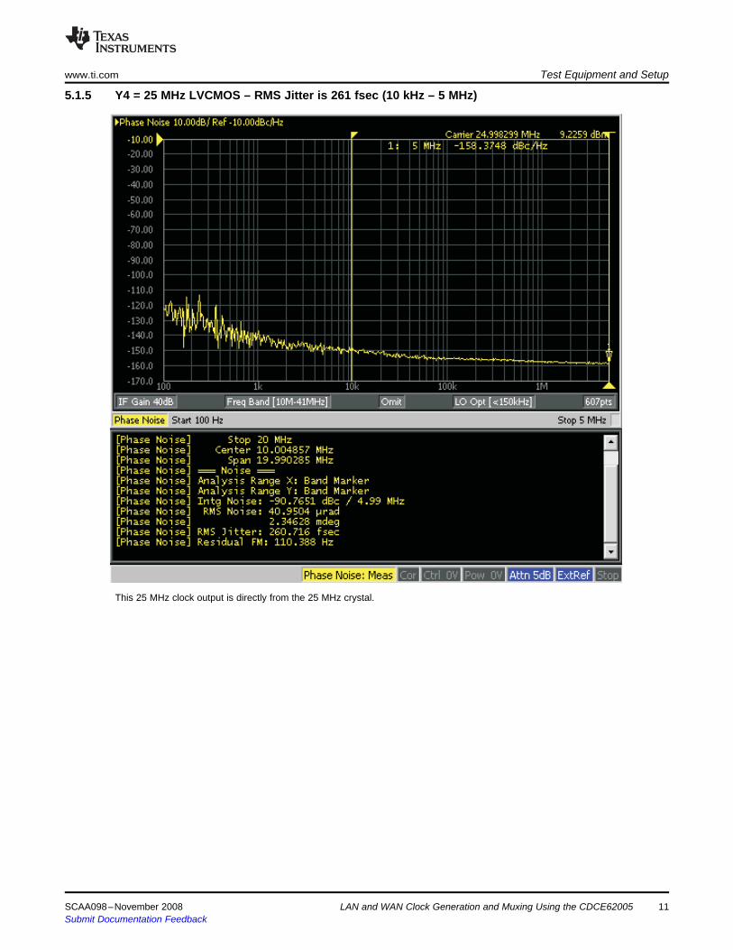
5.1.5 Y4 = 25 MHz LVCMOS – RMS Jitter is 261 fsec (10 kHz – 5 MHz)
www.ti.com Test Equipment and Setup
This 25 MHz clock output is directly from the 25 MHz crystal.
SCAA098–November 2008 LAN and WAN Clock Generation and Muxing Using the CDCE62005 11Submit Documentation Feedback
CDCE62005
Synthesizer24.8832 MHz
Y0: 77.76 MHz LVDS
Y1: 311.04 MHz LVPECL
Y2: 155.52 MHz LVPECL
Y3: 2x17.44 MHz 3.3 V LVCPECL
Y4: 622.08 MHz LVPECL
Test Equipment and Setup www.ti.com
Figure 8. Setup Configuration # 2
Figure 9. TI GUI Setup Configuration # 2
LAN and WAN Clock Generation and Muxing Using the CDCE6200512 SCAA098–November 2008Submit Documentation Feedback
5.2 Configuration #2 Phase Noise Plot Results
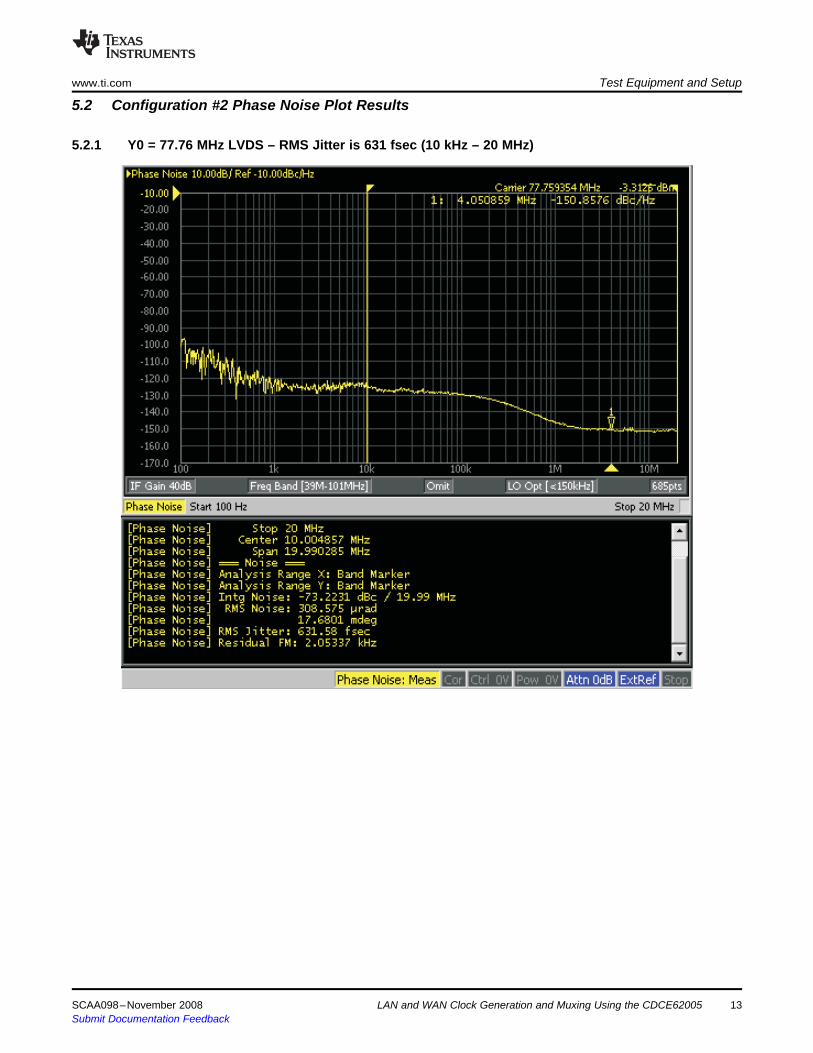
5.2.1 Y0 = 77.76 MHz LVDS – RMS Jitter is 631 fsec (10 kHz – 20 MHz)
www.ti.com Test Equipment and Setup
SCAA098–November 2008 LAN and WAN Clock Generation and Muxing Using the CDCE62005 13Submit Documentation Feedback
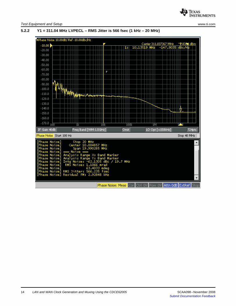
5.2.2 Y1 = 311.04 MHz LVPECL – RMS Jitter is 566 fsec (1 kHz – 20 MHz)
Test Equipment and Setup www.ti.com
LAN and WAN Clock Generation and Muxing Using the CDCE6200514 SCAA098–November 2008Submit Documentation Feedback
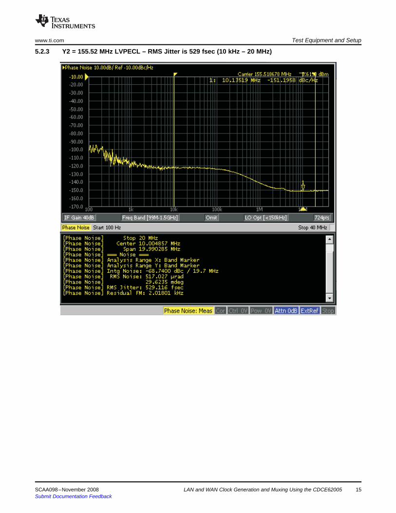
5.2.3 Y2 = 155.52 MHz LVPECL – RMS Jitter is 529 fsec (10 kHz – 20 MHz)
www.ti.com Test Equipment and Setup
SCAA098–November 2008 LAN and WAN Clock Generation and Muxing Using the CDCE62005 15Submit Documentation Feedback
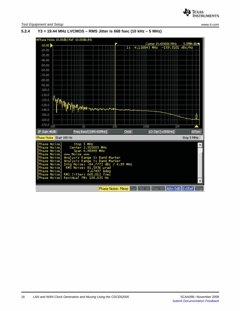
5.2.4 Y3 = 19.44 MHz LVCMOS – RMS Jitter is 668 fsec (10 kHz – 5 MHz)
Test Equipment and Setup www.ti.com
LAN and WAN Clock Generation and Muxing Using the CDCE6200516 SCAA098–November 2008Submit Documentation Feedback
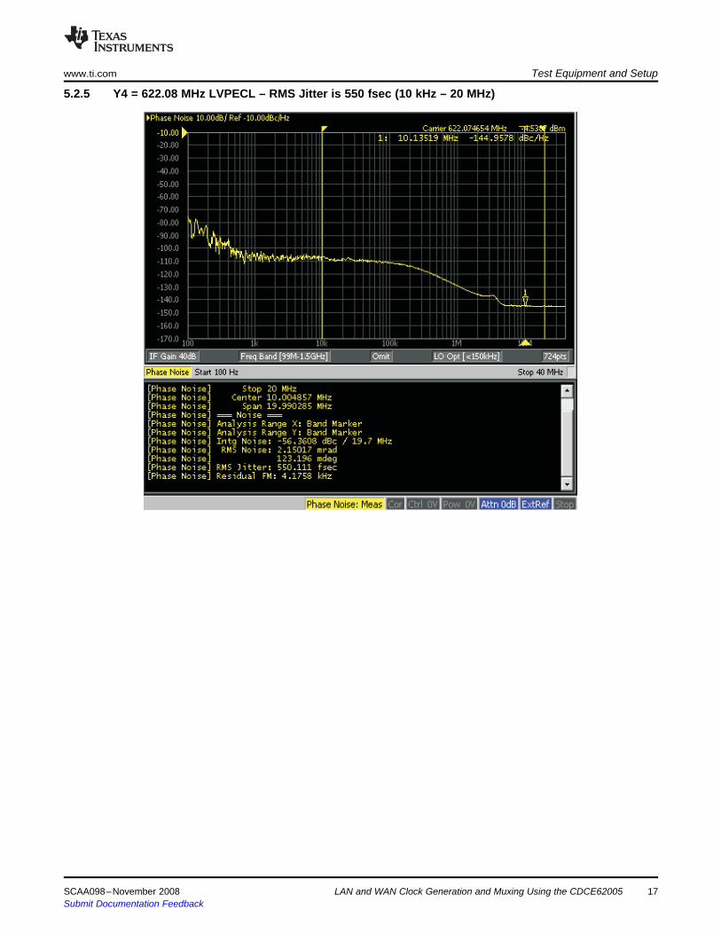
5.2.5 Y4 = 622.08 MHz LVPECL – RMS Jitter is 550 fsec (10 kHz – 20 MHz)
www.ti.com Test Equipment and Setup
SCAA098–November 2008 LAN and WAN Clock Generation and Muxing Using the CDCE62005 17Submit Documentation Feedback
CDCE62005
Synthesizer
#2
CDCE62005
Synthesizer
#1
SPI
25 MHz
Y0: 156.25 MHz or 155.52 KHz LVDS
Y1: 153.25 MHz or 155.52 MHz LVPECL
Y2: 156.25 MHz or 155.52 MHz LVPECL
Y3: 156.25 MHz or 155.52 MHz LVDS
24.8832 MHz
U1: 156.25 MHz or 155.52 KHz LVPECL
U2: 153.25 MHz or 155.52 MHz LVPECL
U3: 156.25 MHz or 155.52 MHz LVDS
U4: 156.25 MHz or 155.52 MHz LVPECL
Test Equipment and Setup www.ti.com
Figure 10. Setup Configuration # 3
Figure 11. TI GUI Setup Configuration # 3 – CDCE62005 #1
18 LAN and WAN Clock Generation and Muxing Using the CDCE62005 SCAA098–November 2008Submit Documentation Feedback
www.ti.com Test Equipment and Setup
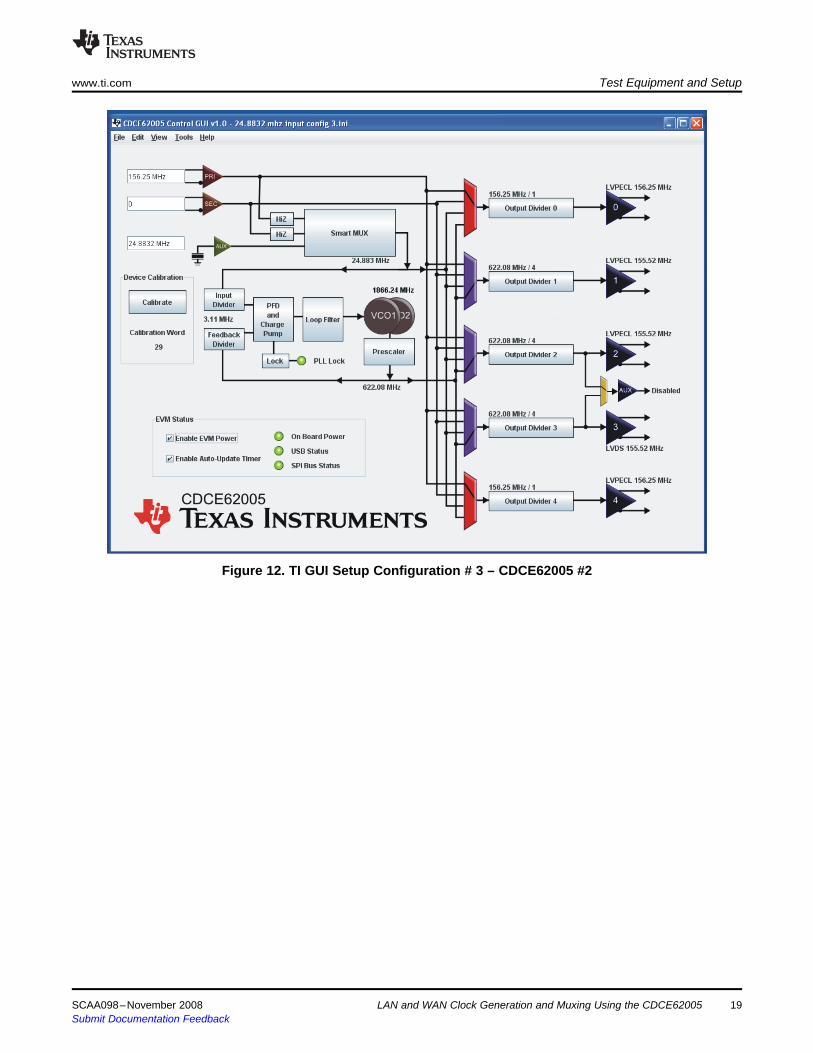
Figure 12. TI GUI Setup Configuration # 3 – CDCE62005 #2
SCAA098–November 2008 LAN and WAN Clock Generation and Muxing Using the CDCE62005 19Submit Documentation Feedback
5.3 Configuration #3 Phase Noise Plot Results
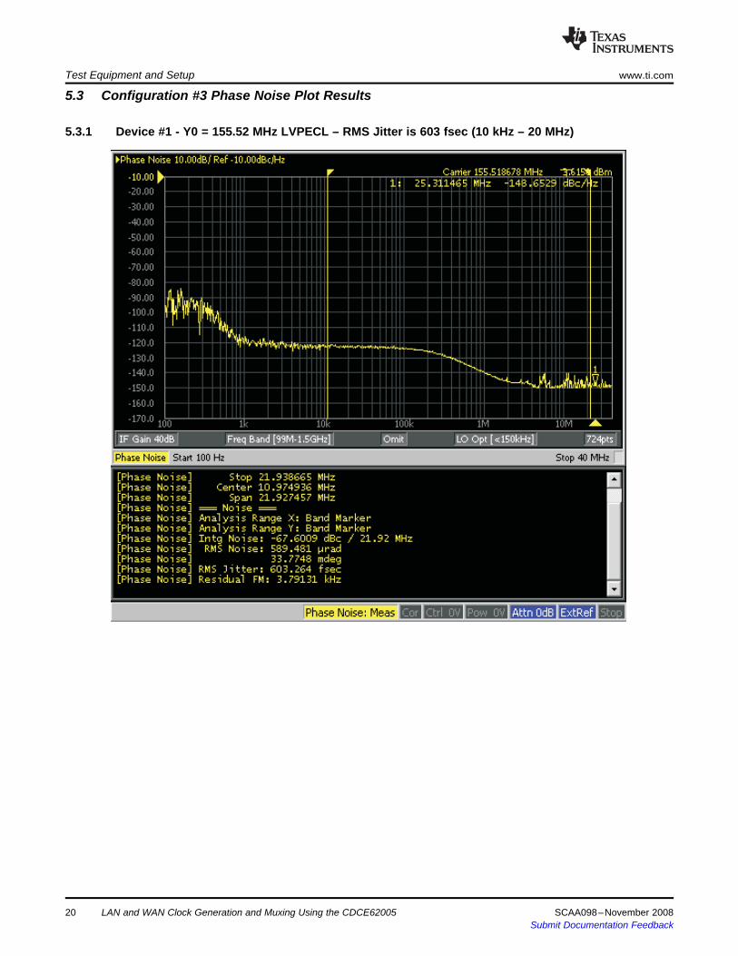
5.3.1 Device #1 - Y0 = 155.52 MHz LVPECL – RMS Jitter is 603 fsec (10 kHz – 20 MHz)
Test Equipment and Setup www.ti.com
LAN and WAN Clock Generation and Muxing Using the CDCE6200520 SCAA098–November 2008Submit Documentation Feedback
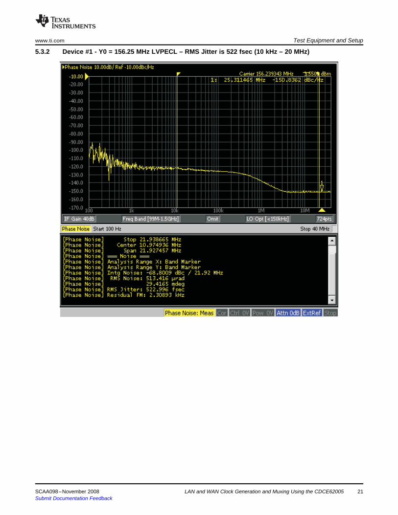
5.3.2 Device #1 - Y0 = 156.25 MHz LVPECL – RMS Jitter is 522 fsec (10 kHz – 20 MHz)
www.ti.com Test Equipment and Setup
SCAA098–November 2008 LAN and WAN Clock Generation and Muxing Using the CDCE62005 21Submit Documentation Feedback
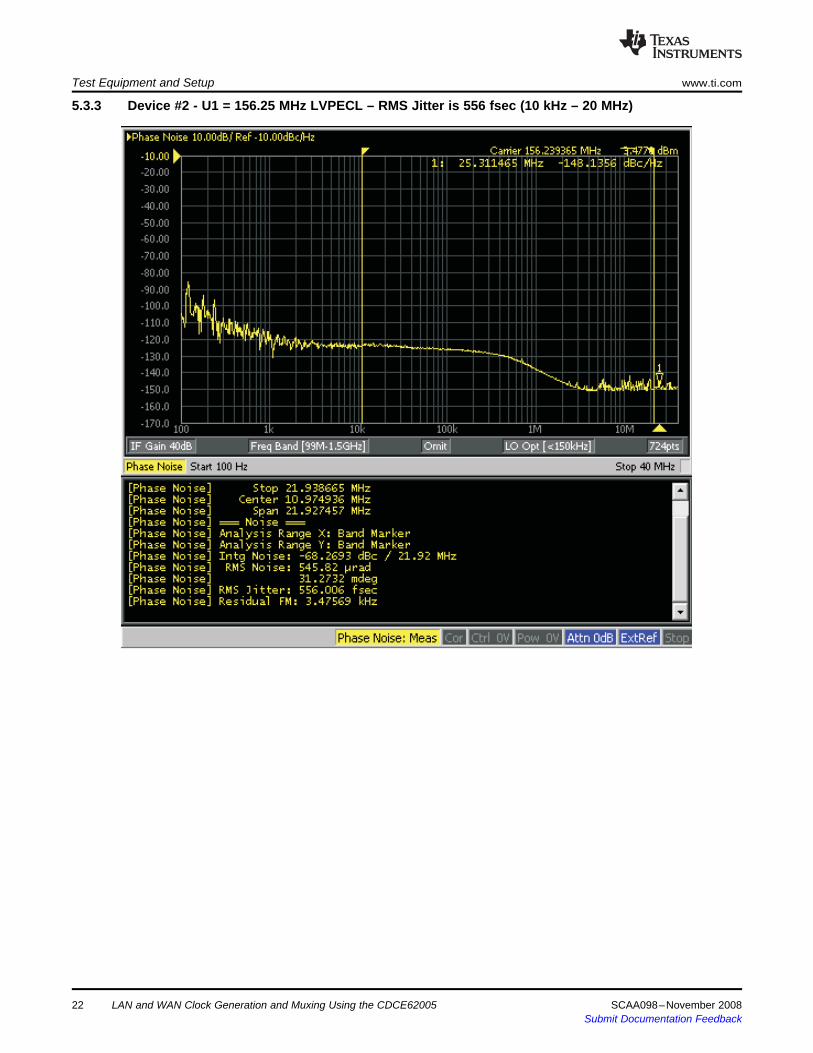
5.3.3 Device #2 - U1 = 156.25 MHz LVPECL – RMS Jitter is 556 fsec (10 kHz – 20 MHz)
Test Equipment and Setup www.ti.com
LAN and WAN Clock Generation and Muxing Using the CDCE6200522 SCAA098–November 2008Submit Documentation Feedback

5.3.4 Device #2 - U1 = 155.52 MHz LVPECL – RMS Jitter is 576 fsec (10 kHz – 20 MHz)
www.ti.com Test Equipment and Setup
SCAA098–November 2008 LAN and WAN Clock Generation and Muxing Using the CDCE62005 23Submit Documentation Feedback
CDCE62005
Synthesizer25 MHz
Y0: 1.5 GHz LVPECL
Y2: 2x125 MHz LVCMOS
Y3: 156.25 MHz LVDS
Y4: 2x133.33 MHz / 66.66 MHz / 33.33 MHz - LVCMOS
133.33 MHz LVPECL
1.5 GHz LVPECL
SPI
Y1: 1.5 GHz LVPECL
Test Equipment and Setup www.ti.com
Figure 13. Setup Configuration # 4
Figure 14. TI GUI Setup Configuration # 4
LAN and WAN Clock Generation and Muxing Using the CDCE6200524 SCAA098–November 2008Submit Documentation Feedback
5.4 Configuration #4 Phase Noise Plot Results
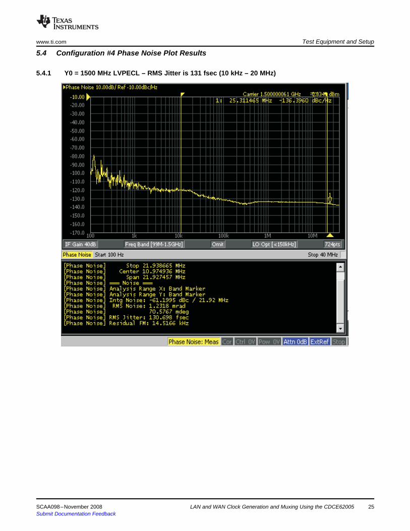
5.4.1 Y0 = 1500 MHz LVPECL – RMS Jitter is 131 fsec (10 kHz – 20 MHz)
www.ti.com Test Equipment and Setup
SCAA098–November 2008 LAN and WAN Clock Generation and Muxing Using the CDCE62005 25Submit Documentation Feedback
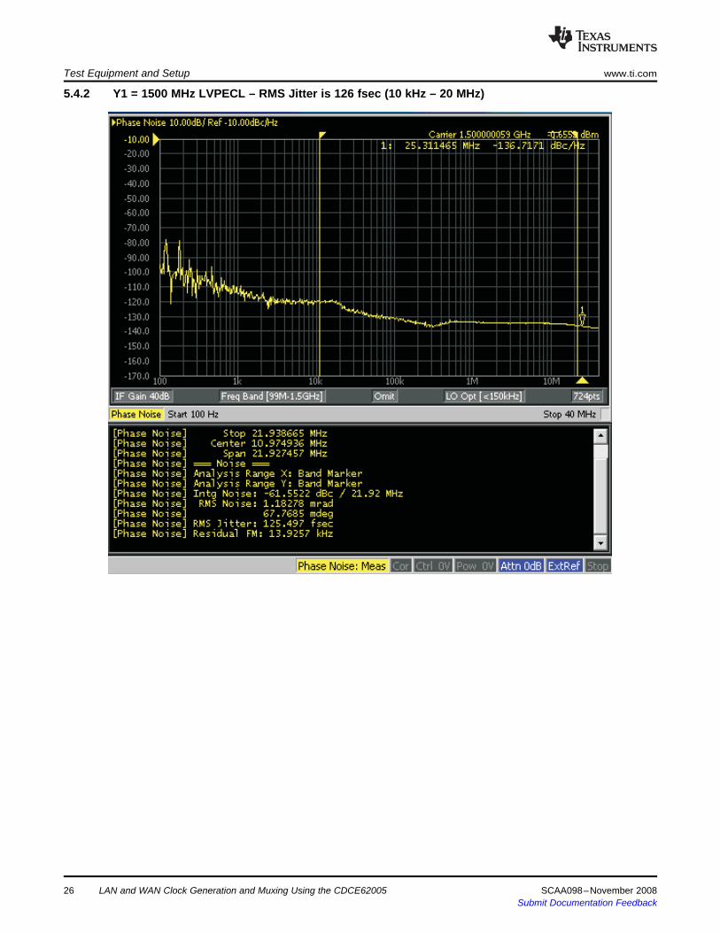
5.4.2 Y1 = 1500 MHz LVPECL – RMS Jitter is 126 fsec (10 kHz – 20 MHz)
Test Equipment and Setup www.ti.com
LAN and WAN Clock Generation and Muxing Using the CDCE6200526 SCAA098–November 2008Submit Documentation Feedback

5.4.3 Y2 = 125 MHz LVCMOS – RMS Jitter is 598 fsec (10 kHz – 20 MHz)
www.ti.com Test Equipment and Setup
SCAA098–November 2008 LAN and WAN Clock Generation and Muxing Using the CDCE62005 27Submit Documentation Feedback
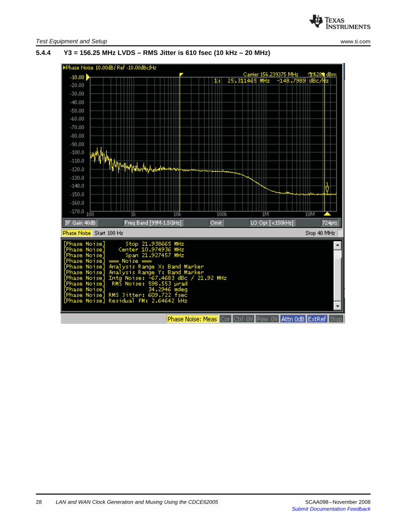
5.4.4 Y3 = 156.25 MHz LVDS – RMS Jitter is 610 fsec (10 kHz – 20 MHz)
Test Equipment and Setup www.ti.com
LAN and WAN Clock Generation and Muxing Using the CDCE6200528 SCAA098–November 2008Submit Documentation Feedback
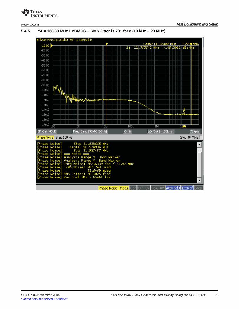
5.4.5 Y4 = 133.33 MHz LVCMOS – RMS Jitter is 701 fsec (10 kHz – 20 MHz)
www.ti.com Test Equipment and Setup
SCAA098–November 2008 LAN and WAN Clock Generation and Muxing Using the CDCE62005 29Submit Documentation Feedback
6 Performance Summary
6.1 Configuration #1
6.2 Configuration #2
6.3 Configuration #3
Performance Summary www.ti.com
Performance results of this LAN configuration are:• Y0 = 125 MHz LVDS – RMS Jitter is 540.65 fsec (10 kHz–20 MHz)• Y1 = 312.5 MHz LVPECL – RMS Jitter is 544.445 fsec (10 kHz–20 MHz)• Y2 = 156.25 MHz LVPECL – RMS Jitter is 520.358 fsec (10 kHz–20 MHz)• Y3 = 625 MHz LVPECL – RMS Jitter is 447.949 fsec (10 kHz–20 MHz)• Y4 = 25 MHz LVCMOS – RMS Jitter is 260.716 fsec (10 kHz–5 MHz)
All the above frequencies are generated by a standard 25MHz input crystal. Y4 is a bypass of the inputcrystal and is not generated from the internal VCO core.
Performance results of this WAN configuration are:• Y0 = 77.76 MHz LVDS – RMS Jitter is 631.58 fsec (10 kHz–20 MHz)• Y1 = 311.04 MHz LVPECL – RMS Jitter is 566.235 fsec (10 kHz–20 MHz)• Y2 = 155.52 MHz LVPECL – RMS Jitter is 529.116 fsec (10 kHz–20 MHz)• Y3 = 19.44 MHz LVCMOS – RMS Jitter is 668.012 fsec (10 kHz–5 MHz)• Y4 = 622.08 MHz LVPECL – RMS Jitter is 550.111 fsec (10 kHz–20 MHz)
Performance results of this LAN/WAN configuration are:• Device #1 : Y0 = 155.52 MHz LVPECL – RMS Jitter is 603.264 fsec (10 kHz–20 MHz)• Device #1 : Y0 = 156.25 MHz LVPECL – RMS Jitter is 522.996 fsec (10 kHz–20 MHz)• Device #2 : U1 = 156.25 MHz LVPECL – RMS Jitter is 556.006 fsec (10 kHz–20 MHz)• Device #2 : U1 = 155.52 MHz LVPECL– RMS Jitter is 576.166 fsec (10 kHz –20 MHz)
In this example, only the measurement data is shown for device #1 output Y0 and device #2 output U1 at155.52 MHz and then switched to 156.25MHz. All other outputs (Y1-Y4; U0,U2-U4) will showapproximately the same jitter as they are just copies of the same frequency. Remember that device #1bypasses the 155.52MHz from the output of device #2 output U0, so the additive jitter of the CDCE62005device # 1 output Y0 can be calculated as follows:
Additive jitter at device #1 output Y0 = √(Y02 – U02)= √(603.2642 – 576.1662)= 178.7741 fsec RMS
Assume that U0 = ≈U1.
The same applies for calculating the additive jitter of device # 2 when the 156.25MHz is bypassed fromdevice #1 Y4
Additive jitter at device #2 output U1 = √(U12 – Y42)= √(556.0062 – 522.9962)= 188.7269 fsec RMS
Assume that Y4 = ≈Y0.
LAN and WAN Clock Generation and Muxing Using the CDCE6200530 SCAA098–November 2008Submit Documentation Feedback
6.4 Configuration #4
7 Conclusion
www.ti.com Conclusion
Performance results of this general purpose configuration are:• Y0 = 1500 MHz LVPECL – RMS Jitter is 130.698 fsec (10 kHz–20 MHz)• Y1 = 1500 MHz LVPECL – RMS Jitter is 125.497 fsec (10 kHz–20 MHz)• Y2 = 125 MHz LVCMOS – RMS Jitter is 597.782 fsec (10 kHz–20 MHz)• Y3 = 156.25 MHz LVDS – RMS Jitter is 609.722 fsec (10 kHz–20 MHz)• Y4 = 133.33 MHz LVCMOS – RMS Jitter is 701.025 fsec (10 kHz – 20 MHz)
In this example there are 3 clocks that are bypassed for the input and 2 clocks that are generated by theinternal VCO core.
Input jitter of the 1500 MHz clock at PRI_IN is 120 fsec RMS.
Input jitter of the 133.33 MHz clock at SEC_IN is 512 fsec RMS.
Additive jitter can then be calculated as:
Y0 additive jitter = √(Y0 total output jitter2 – Input jitter2)= √(130.6892 – 1202)= 51.765 fsec RMS
Y1 additive jitter = √(Y1 total output jitter2 – Input jitter2)= √(125.4972 – 1202)= 36.7355 fsec RMS
Y4 additive jitter = √(Y4 total output jitter2 – Input jitter2)= √(701.0252 – 5122)= 478.8445 fsec RMS
The CDCE62005 performance meets networking frequencies and low jitter requirements <1ps RMS. It is aflexible device that can be configured in a number of ways to meet specific system needs.
The CDCE62005 is offered in a 48-pin 6mm × 6mm QFN package. This single, 3.3 V device can replacethe functionality of multiple expensive oscillators, clock muxes, and buffers. In addition to lowering cost,the CDCE62005 offers additional advances features like output phase adjust and mixed output signallevels. Either through the SPI bus or EEPROM, the required frequencies can be generated.
SCAA098–November 2008 LAN and WAN Clock Generation and Muxing Using the CDCE62005 31Submit Documentation Feedback
IMPORTANT NOTICETexas Instruments Incorporated and its subsidiaries (TI) reserve the right to make corrections, modifications, enhancements, improvements,and other changes to its products and services at any time and to discontinue any product or service without notice. Customers shouldobtain the latest relevant information before placing orders and should verify that such information is current and complete. All products aresold subject to TI’s terms and conditions of sale supplied at the time of order acknowledgment.TI warrants performance of its hardware products to the specifications applicable at the time of sale in accordance with TI’s standardwarranty. Testing and other quality control techniques are used to the extent TI deems necessary to support this warranty. Except wheremandated by government requirements, testing of all parameters of each product is not necessarily performed.TI assumes no liability for applications assistance or customer product design. Customers are responsible for their products andapplications using TI components. To minimize the risks associated with customer products and applications, customers should provideadequate design and operating safeguards.TI does not warrant or represent that any license, either express or implied, is granted under any TI patent right, copyright, mask work right,or other TI intellectual property right relating to any combination, machine, or process in which TI products or services are used. Informationpublished by TI regarding third-party products or services does not constitute a license from TI to use such products or services or awarranty or endorsement thereof. Use of such information may require a license from a third party under the patents or other intellectualproperty of the third party, or a license from TI under the patents or other intellectual property of TI.Reproduction of TI information in TI data books or data sheets is permissible only if reproduction is without alteration and is accompaniedby all associated warranties, conditions, limitations, and notices. Reproduction of this information with alteration is an unfair and deceptivebusiness practice. TI is not responsible or liable for such altered documentation. Information of third parties may be subject to additionalrestrictions.Resale of TI products or services with statements different from or beyond the parameters stated by TI for that product or service voids allexpress and any implied warranties for the associated TI product or service and is an unfair and deceptive business practice. TI is notresponsible or liable for any such statements.TI products are not authorized for use in safety-critical applications (such as life support) where a failure of the TI product would reasonablybe expected to cause severe personal injury or death, unless officers of the parties have executed an agreement specifically governingsuch use. Buyers represent that they have all necessary expertise in the safety and regulatory ramifications of their applications, andacknowledge and agree that they are solely responsible for all legal, regulatory and safety-related requirements concerning their productsand any use of TI products in such safety-critical applications, notwithstanding any applications-related information or support that may beprovided by TI. Further, Buyers must fully indemnify TI and its representatives against any damages arising out of the use of TI products insuch safety-critical applications.TI products are neither designed nor intended for use in military/aerospace applications or environments unless the TI products arespecifically designated by TI as military-grade or "enhanced plastic." Only products designated by TI as military-grade meet militaryspecifications. Buyers acknowledge and agree that any such use of TI products which TI has not designated as military-grade is solely atthe Buyer's risk, and that they are solely responsible for compliance with all legal and regulatory requirements in connection with such use.TI products are neither designed nor intended for use in automotive applications or environments unless the specific TI products aredesignated by TI as compliant with ISO/TS 16949 requirements. Buyers acknowledge and agree that, if they use any non-designatedproducts in automotive applications, TI will not be responsible for any failure to meet such requirements.Following are URLs where you can obtain information on other Texas Instruments products and application solutions:Products ApplicationsAmplifiers amplifier.ti.com Audio www.ti.com/audioData Converters dataconverter.ti.com Automotive www.ti.com/automotiveDSP dsp.ti.com Broadband www.ti.com/broadbandClocks and Timers www.ti.com/clocks Digital Control www.ti.com/digitalcontrolInterface interface.ti.com Medical www.ti.com/medicalLogic logic.ti.com Military www.ti.com/militaryPower Mgmt power.ti.com Optical Networking www.ti.com/opticalnetworkMicrocontrollers microcontroller.ti.com Security www.ti.com/securityRFID www.ti-rfid.com Telephony www.ti.com/telephonyRF/IF and ZigBee® Solutions www.ti.com/lprf Video & Imaging www.ti.com/video
Wireless www.ti.com/wireless
Mailing Address: Texas Instruments, Post Office Box 655303, Dallas, Texas 75265Copyright © 2008, Texas Instruments Incorporated