laboratory of reliable computing department of electrical engineering national tsing hua university...
Post on 21-Dec-2015
346 views
TRANSCRIPT

Laboratory of Reliable ComputingDepartment of Electrical EngineeringNational Tsing Hua UniversityHsinchu, Taiwan
Delay Defect Characteristics and Delay Defect Characteristics and Testing StrategiesTesting Strategies
Delay Defect Characteristics and Delay Defect Characteristics and Testing StrategiesTesting Strategies
Kee Sup Kim, Subhasish Mitra, and Paul G.Ryan
Design&Test 2003

2
IntroductionIntroductionIntroductionIntroduction A timing failure is case that circuit can’t operate
correctly at the specified speed setup time violation hold time violation
This paper discusses delay defect characteristic impact on IC quality testing strategy
XX
hshs

3
What Significance of Delay Defect?What Significance of Delay Defect?What Significance of Delay Defect?What Significance of Delay Defect? Output response for 30% to 35% of defective
parts depend on the test speed. (VTS02)
Delay defects have typically represented 1% to 5% of the total defect population observed. (Intel)
At-speed functional testing is cost prohibitive on-chip clock source ATE cost/test pattern generation low voltage testing
4
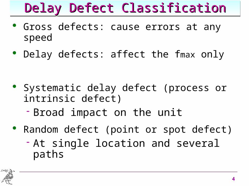
Delay Defect ClassificationDelay Defect ClassificationDelay Defect ClassificationDelay Defect Classification Gross defects: cause errors at any speed
Delay defects: affect the fmax only
Systematic delay defect (process or intrinsic defect) Broad impact on the unit
Random defect (point or spot defect) At single location and several paths
5
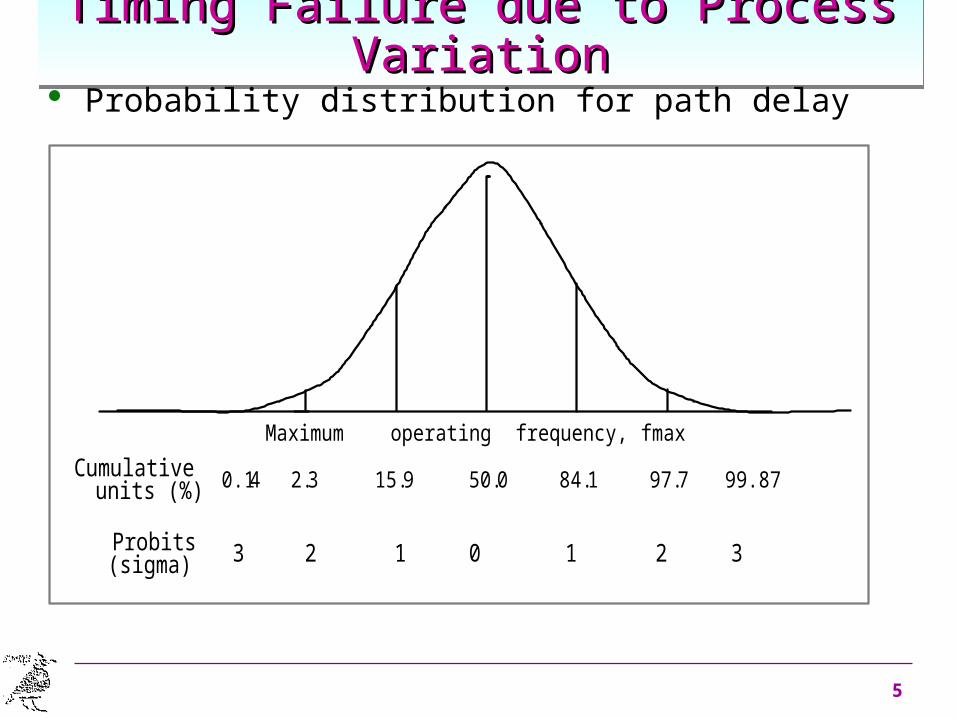
Timing Failure due to Process VariationTiming Failure due to Process VariationTiming Failure due to Process VariationTiming Failure due to Process Variation Probability distribution for path delay
operatingMaximumCumulative
units (%)
Probits(sigma) 3 12 0 1 2 3
frequency, f max
40.1 3 15.9 50.0 84.1 97.7 99.872.

6
Solutions to Process Timing FailureSolutions to Process Timing FailureSolutions to Process Timing FailureSolutions to Process Timing Failure Choice of product’s operating frequency
economic tradeoff
Speed binning: to distinguish faster parts to be sold at a higher
price
Over-design: increase the die size, power, and packages cost

7
Characteristic of Speed Failure Characteristic of Speed Failure Characteristic of Speed Failure Characteristic of Speed Failure First-fail data from microprocessor (.18m)
Process variation -> critical path Random defect -> any locations
No.
of u
nits
Fail Signature

8
Distinguishing of DefectsDistinguishing of DefectsDistinguishing of DefectsDistinguishing of Defects Two complementary techniques to differentiate
random defects and process variation
Signature-based approach analyze the number of units sharing each fail
signature random defects on critical path
Frequency distribution technique Analyze the fmax data for all units sharing a
common signature

9
Histogram of Histogram of ffmaxmaxHistogram of Histogram of ffmaxmax
Normal process variation results in fmax values with a Gaussian distribution
No.
of u
nits
Maximum operating frequency

10
Delay Testing TechniquesDelay Testing TechniquesDelay Testing TechniquesDelay Testing Techniques Some delay defect can be detected by process
monitor ring oscillators trees of NAND gates with controlled delays
Boolean testing at some clock frequency test pattern generation? at what clock frequency?

11
Test Pattern for Systematic Delay DefectTest Pattern for Systematic Delay DefectTest Pattern for Systematic Delay DefectTest Pattern for Systematic Delay Defect Systematic delay problem caused by process
variation will affect several paths including the critical path
Functional test patterns are manually written by designers
Advantage it can be exercised in the system
Disadvantage difficult and cost a lot of time

12
Test Pattern for Random Delay DefectTest Pattern for Random Delay DefectTest Pattern for Random Delay DefectTest Pattern for Random Delay Defect Comparing to the systematic defects, additional
test patterns covering the entire design are required
Using the path delay fault model complexity issue
Using the transition-fault model total number of transition fault 100% fault coverage EDA tool support without timing analysis

13
Impact of Inaccurate Timing analysisImpact of Inaccurate Timing analysisImpact of Inaccurate Timing analysisImpact of Inaccurate Timing analysis Static timing analysis/dynamic timing analysis
gate delay, interconnection delay
Many physical factor affect the accuracy voltage, temperature, skew, cross-talk, …
For large designs, the center and the edge may exhibit different speed
A fault model for delay defect must not be critically dependent on accurate timing analysis

14
Limitation of Transition Fault ModelLimitation of Transition Fault ModelLimitation of Transition Fault ModelLimitation of Transition Fault Model Which path excites a transition fault or
propagates the fault effect does not consider If the fault effect propagates from the fault site
along a very short path with a lot time slack ATPG issue?
9
Fault-free site3
6Fault site
3
6

15
Test Pattern with Scan-based TestTest Pattern with Scan-based TestTest Pattern with Scan-based TestTest Pattern with Scan-based Test Approaches to generating a pair of test patterns
with scan: One memory element
Skewed-load or launch-on-last-shift Double-pulse or launch-on-capture
Two memory element LSSD
False path problem paths is detected but cannot exercised during
normal operations yield-loss

16
Launch-on-Shift ScanLaunch-on-Shift ScanLaunch-on-Shift ScanLaunch-on-Shift Scan
V2 is shifted version of V1 (un-testable fault)
SE routing is critical
ATPG is easy

17
Launch-on-CaptureLaunch-on-CaptureLaunch-on-CaptureLaunch-on-Capture
SE routing is easy
ATPG is more complex

18
Effectiveness of TF TestingEffectiveness of TF TestingEffectiveness of TF TestingEffectiveness of TF Testing ASIC1 (0.18m) with 800K gates from LSI Logic
IEEE D&T 2003
Test Method No. of scan partitions
TF coverage
Test freq.
Defect coverage
At-speed functional 30% 160M 30%Launch-on-capture 8,495 72.45% 100M 57%Launch-on-shift 4,200 80.10% 20M 28%

19
Effectiveness of TF Testing (cont.)Effectiveness of TF Testing (cont.)Effectiveness of TF Testing (cont.)Effectiveness of TF Testing (cont.) Venn diagram of test results
8080
74741616
1919
0033 5353
Launch-on-captureLaunch-on-capture
At-speed functionalAt-speed functionalLaunch-on-shiftLaunch-on-shift
Total 245 unitsTotal 245 units

20
More Issues?More Issues?More Issues?More Issues? Multiple clock domains
High performance application How fast to apply clock Most solutions increase the complexity of ATPG
Z1Z
nX+1mXmX
C11Y1
circuitN2
X1
D1 q
r
1 Y1
qs YkC1
D1C1
D1C1
Combinational Combinational
q
Zr+1Clk2Clk1 Zt
D1 qk
YscircuitN1

21
ConclusionConclusionConclusionConclusion Overdesign cannot guarantee all parts pass the
delay defect screening
For systematic delay defects process monitor critical-paths delay testing
For random defects transition-fault testing is necessary
Test compression is considered due to test economics