lab manual - vvitengineeringvvitengineering.com/lab/ee6611-power-electronic… · · 2016-12-31if...
TRANSCRIPT

EE6611 POWER ELECTRONICS AND DRIVES LABORATORY 1
VVIT DEPARTMENT OF ELECTRICAL AND ELECTRONICS ENGINEERING
Dharmapuri – 636 703
Regulation : 2013
Branch : B.E - EEE
Year & Semester : III Year / VI Semester
LAB MANUAL
EE6611- POWER ELECTRONICS AND DRIVESLABORATORY

EE6611 POWER ELECTRONICS AND DRIVES LABORATORY 2
VVIT DEPARTMENT OF ELECTRICAL AND ELECTRONICS ENGINEERING
ANNA UNIVERSITY
SYLLABUS (2013 REGULATION)
SEMESTER VI
EE6611 - POWER ELECTRONICS AND DRIVES LABORATORY
LIST OF EXPERIMENTS:
1. Gate Pulse Generation using R, RC and UJT.
2. Characteristics of SCR and Triac
3. Characteristics of MOSFET and IGBT
4. AC to DC half controlled converter
5. AC to DC fully controlled Converter
6. Step down and step up MOSFET based choppers
7. IGBT based single phase PWM inverter
8. IGBT based three phase PWM inverter
9. AC Voltage controller
10. Switched mode power converter.
11. Simulation of PE circuits (1Φ&3Φsemiconverter, 1Φ&3Φfullconverter, dc-dc
Converters, ac voltage controllers).
TOTAL :45 Hours

EE6611 POWER ELECTRONICS AND DRIVES LABORATORY 3
VVIT DEPARTMENT OF ELECTRICAL AND ELECTRONICS ENGINEERING
CYCLE I
1. Gate Pulse Generation using R, RC and UJT.
2. Characteristics of SCR and Triac
3. Characteristics of MOSFET and IGBT
4. AC to DC half controlled converter
5. AC to DC fully controlled Converter
6. Step down and step up MOSFET based choppers
CYCLE II
7. IGBT based single phase PWM inverter
8. IGBT based three phase PWM inverter
9. AC Voltage controller
10. Switched mode power converter.
11. Simulation of PE circuits (1Φ&3Φsemiconverter, 1Φ&3Φfullconverter, dc-dc
Converters, ac voltage controllers).

EE6611 POWER ELECTRONICS AND DRIVES LABORATORY 4
VVIT DEPARTMENT OF ELECTRICAL AND ELECTRONICS ENGINEERING
INDEXS. No. DATE NAME OF THE EXPERIMENT SIGNATURE REMARKS
1 Gate Pulse Generation using R, RC and UJT
2 Characteristics of SCR
3 Characteristics of Triac
4 Characteristics of MOSFET and IGBT
5 AC to DC half controlled converter
6 AC to DC fully controlled Converter
7 Step down and step up MOSFET based choppers
8IGBT based single phase PWM inverter
9 IGBT based three phase PWM inverter
10 AC Voltage controller
11 Switched mode power converter
12 Simulation of Single Phase semi converter
13 Simulation of Single Phase Full Converter
14Simulation of Single Phase AC Voltage ControlUsing TRIAC
15 Simulation of DC-DC Converter
16 Simulation of Three Phase Converter
EE6611 POWER ELECTRONICS AND DRIVES LABORATORY 5
VVIT DEPARTMENT OF ELECTRICAL AND ELECTRONICS ENGINEERING
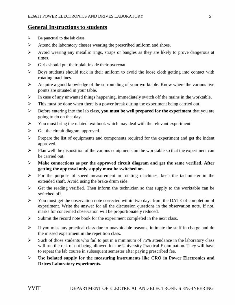
General Instructions to students
Be punctual to the lab class.
Attend the laboratory classes wearing the prescribed uniform and shoes.
Avoid wearing any metallic rings, straps or bangles as they are likely to prove dangerous attimes.
Girls should put their plait inside their overcoat
Boys students should tuck in their uniform to avoid the loose cloth getting into contact withrotating machines.
Acquire a good knowledge of the surrounding of your worktable. Know where the various livepoints are situated in your table.
In case of any unwanted things happening, immediately switch off the mains in the worktable.
This must be done when there is a power break during the experiment being carried out.
Before entering into the lab class, you must be well prepared for the experiment that you aregoing to do on that day.
You must bring the related text book which may deal with the relevant experiment.
Get the circuit diagram approved.
Prepare the list of equipments and components required for the experiment and get the indentapproved.
Plan well the disposition of the various equipments on the worktable so that the experiment canbe carried out.
Make connections as per the approved circuit diagram and get the same verified. Aftergetting the approval only supply must be switched on.
For the purpose of speed measurement in rotating machines, keep the tachometer in theextended shaft. Avoid using the brake drum side.
Get the reading verified. Then inform the technician so that supply to the worktable can beswitched off.
You must get the observation note corrected within two days from the DATE of completion ofexperiment. Write the answer for all the discussion questions in the observation note. If not,marks for concerned observation will be proportionately reduced.
Submit the record note book for the experiment completed in the next class.
If you miss any practical class due to unavoidable reasons, intimate the staff in charge and dothe missed experiment in the repetition class.
Such of those students who fail to put in a minimum of 75% attendance in the laboratory classwill run the risk of not being allowed for the University Practical Examination. They will haveto repeat the lab course in subsequent semester after paying prescribed fee.
Use isolated supply for the measuring instruments like CRO in Power Electronics andDrives Laboratory experiments.

EE6611 POWER ELECTRONICS AND DRIVES LABORATORY 6
VVIT DEPARTMENT OF ELECTRICAL AND ELECTRONICS ENGINEERING
INTRODUCTION
Power electronics studies the application of semiconductor devices to the conversion and
control of electrical energy. The field is driving an era of rapid change in all aspects of electrical
energy. Power electronics is a broad area. Experts in the field find a need for knowledge in advanced
circuit theory, electric power equipment, electromagnetic design, radiation, semiconductor physics
and processing, analog and digital circuit design, control systems, and a tremendous range of sub-
areas. Major applications addressed by power electronics include: Energy conversion for solar, wind,
fuel cell, and other alternative resources. Advanced high-power low-voltage power supplies for
computers and integrated electronics. Efficient low-power supplies for networks and portable
products. Hardware to implement intelligent electricity grids, at all levels.
Power conversion needs and power controllers for aircraft, spacecraft, and marine use.
Electronic controllers for motor drives and other industrial equipment. · Drives and chargers for
electric and hybrid vehicles. · Uninterruptible power supplies for backup power or critical needs.
High-voltage direct current transmission equipment and other power processing in utility systems.
Small, highly efficient, switching power supplies for general use. Such a broad range of topics
requires many years of training and experience in electrical engineering.
Power electronics is the application of solid-state electronics to the control and conversion
of electric power. It also refers to a subject of research in electronic and electrical engineering which
deals with the design, control, computation and integration of nonlinear, time-varying energy-
processing electronic systems with fast dynamics.
The first high power electronic devices were mercury-arc valves. In modern systems the
conversion is performed with semiconductor switching devices such
as diodes, thyristors and transistors, pioneered by R. D. Middle brook and others beginning in the
1950s. In contrast to electronic systems concerned with transmission and processing of signals and
data, in power electronics substantial amounts of electrical energy are processed. An AC/DC
converter (rectifier) is the most typical power electronics device found in many consumer electronic
devices, e.g. television sets, personal computers, battery chargers, etc. The power range is typically
from tens of watts to several hundred watts. In industry a common application is the variable speed
drive (VSD) that is used to control an induction motor. The power range of VSDs start from a few
hundred watts and end at tens of megawatts.

EE6611 POWER ELECTRONICS AND DRIVES LABORATORY 7
VVIT DEPARTMENT OF ELECTRICAL AND ELECTRONICS ENGINEERING
The power conversion systems can be classified according to the type of the input and output power
AC to DC (rectifier)
DC to AC (inverter)
DC to DC (DC-to-DC converter)
AC to AC (AC-to-AC converter)
The objectives of the Power Electronics Laboratory course are to provide working
experience with the power electronics concepts presented in the power electronics lecture course,
while giving students knowledge of the special measurement and design techniques of this subject.
The goal is to give students a "running start," that can lead to a useful understanding of the field in
one semester. The material allows students to design complete switching power supplies by the end
of the semester, and prepares students to interact with power supply builders, designers, and
customers in industry.
Power electronics can be defined as the area that deals with application of electronic
devices for control and conversion of electric power. In particular, a power electronic circuit is
intended to control or convert power at levels far above the device ratings. With this in mind, the
situations encountered in the power electronics laboratory course will often be unusual in an
electronics setting. Safety rules are important, both for the people involved and for the equipment.
Semiconductor devices react very quickly to conditions -- and thus make excellent, expensive,
"fuses."
EE6611 POWER ELECTRONICS AND DRIVES LABORATORY 8
VVIT DEPARTMENT OF ELECTRICAL AND ELECTRONICS ENGINEERING
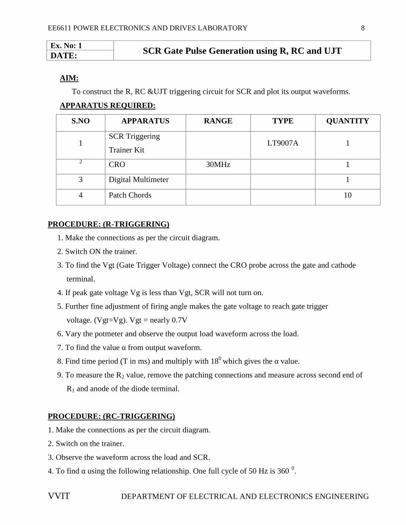
Ex. No: 1SCR Gate Pulse Generation using R, RC and UJTDATE:
AIM:
To construct the R, RC &UJT triggering circuit for SCR and plot its output waveforms.
APPARATUS REQUIRED:
S.NO APPARATUS RANGE TYPE QUANTITY
1SCR Triggering
Trainer KitLT9007A 1
2 CRO 30MHz 1
3 Digital Multimeter 1
4 Patch Chords 10
PROCEDURE: (R-TRIGGERING)
1. Make the connections as per the circuit diagram.
2. Switch ON the trainer.
3. To find the Vgt (Gate Trigger Voltage) connect the CRO probe across the gate and cathode
terminal.
4. If peak gate voltage Vg is less than Vgt, SCR will not turn on.
5. Further fine adjustment of firing angle makes the gate voltage to reach gate trigger
voltage. (Vgt=Vg). Vgt = nearly 0.7V
6. Vary the potmeter and observe the output load waveform across the load.
7. To find the value α from output waveform.
8. Find time period (T in ms) and multiply with 180 which gives the α value.
9. To measure the R2 value, remove the patching connections and measure across second end of
R1 and anode of the diode terminal.
PROCEDURE: (RC-TRIGGERING)
1. Make the connections as per the circuit diagram.
2. Switch on the trainer.
3. Observe the waveform across the load and SCR.
4. To find α using the following relationship. One full cycle of 50 Hz is 360 0.

EE6611 POWER ELECTRONICS AND DRIVES LABORATORY 9
VVIT DEPARTMENT OF ELECTRICAL AND ELECTRONICS ENGINEERING
5. 20ms = 360 0.For example, say 5ms is 5*18=900.
6. Theoretically α value can be found from the following relationship.
Where,
T1 = RC
C= 1 uF
7. R is a variable resistance; this can be found from the terminals A and G. At the time of measuring
the R values the patching connections should be removed.
8. Verify the theoretical value with practical value both more or less equal value.
9. Switch off trainer.
PROCEDURE: (UJT-Triggering)
1. Make the connections as per circuit diagram.
2. Switch On the trainer.
3. Observe the waveform across emitter with respect to ground.
4. To vary the firing angle vary the control pot and observe the output variation in load.
5. To observe the output waveform. Connect the CRO Probe across the load.
6. Find the α value theoretically using the relationship T1 = RC1.
R value can be managed from the terminal provided in the front panel.
The series resistance connected is 150Ω, C1 = 1 uF.
Where,
η = 0.72,
ω = 3 rad/sec
R1 = 150 Ω
7. Verify the theoretical value with the practical value.
α = (T1* 1800) /Half cycle
α = (T1* 1800) /10 ms
α = ωT1 ln(1/1- η)
T1 = (R measure +R1) * C1

EE6611 POWER ELECTRONICS AND DRIVES LABORATORY 10
VVIT DEPARTMENT OF ELECTRICAL AND ELECTRONICS ENGINEERING
CIRCUIT DIAGRAM: (Resistance Firing Circuit)
CIRCUIT DIAGRAM: (RC-Triggering)
EE6611 POWER ELECTRONICS AND DRIVES LABORATORY 10
VVIT DEPARTMENT OF ELECTRICAL AND ELECTRONICS ENGINEERING
CIRCUIT DIAGRAM: (Resistance Firing Circuit)
CIRCUIT DIAGRAM: (RC-Triggering)
EE6611 POWER ELECTRONICS AND DRIVES LABORATORY 10
VVIT DEPARTMENT OF ELECTRICAL AND ELECTRONICS ENGINEERING
CIRCUIT DIAGRAM: (Resistance Firing Circuit)
CIRCUIT DIAGRAM: (RC-Triggering)

EE6611 POWER ELECTRONICS AND DRIVES LABORATORY 11
VVIT DEPARTMENT OF ELECTRICAL AND ELECTRONICS ENGINEERING
CIRCUIT DIAGRAM: (UJT-TRIGGERING)
TABULAR COLUMN: (R-Triggering)
SL. NoResistance.
(R2)Ω
Theoretical Firingangle(α)Degree
Practical Firingangle(α)Degree
Where,
Vgt = 0.7 v
R1 = 1000 Ω
R = 220 Ω
Vm = v
Firing angle (α) =

EE6611 POWER ELECTRONICS AND DRIVES LABORATORY 12
VVIT DEPARTMENT OF ELECTRICAL AND ELECTRONICS ENGINEERING
MODEL GRAPH ( R-TRIGGERING) :
TABULATOR COLUMN: (RC-Triggering)
SL .NoT1 = RC
ms
α (Theoretical)
Degree
Time Periodfrom CRO
ms
α ( Practical)α = T * 180
Degree
Where
T1 = RC
R= 2000 Ω
C = 1 uF
Firing angle (α) = * 180⁰
EE6611 POWER ELECTRONICS AND DRIVES LABORATORY 13
VVIT DEPARTMENT OF ELECTRICAL AND ELECTRONICS ENGINEERING
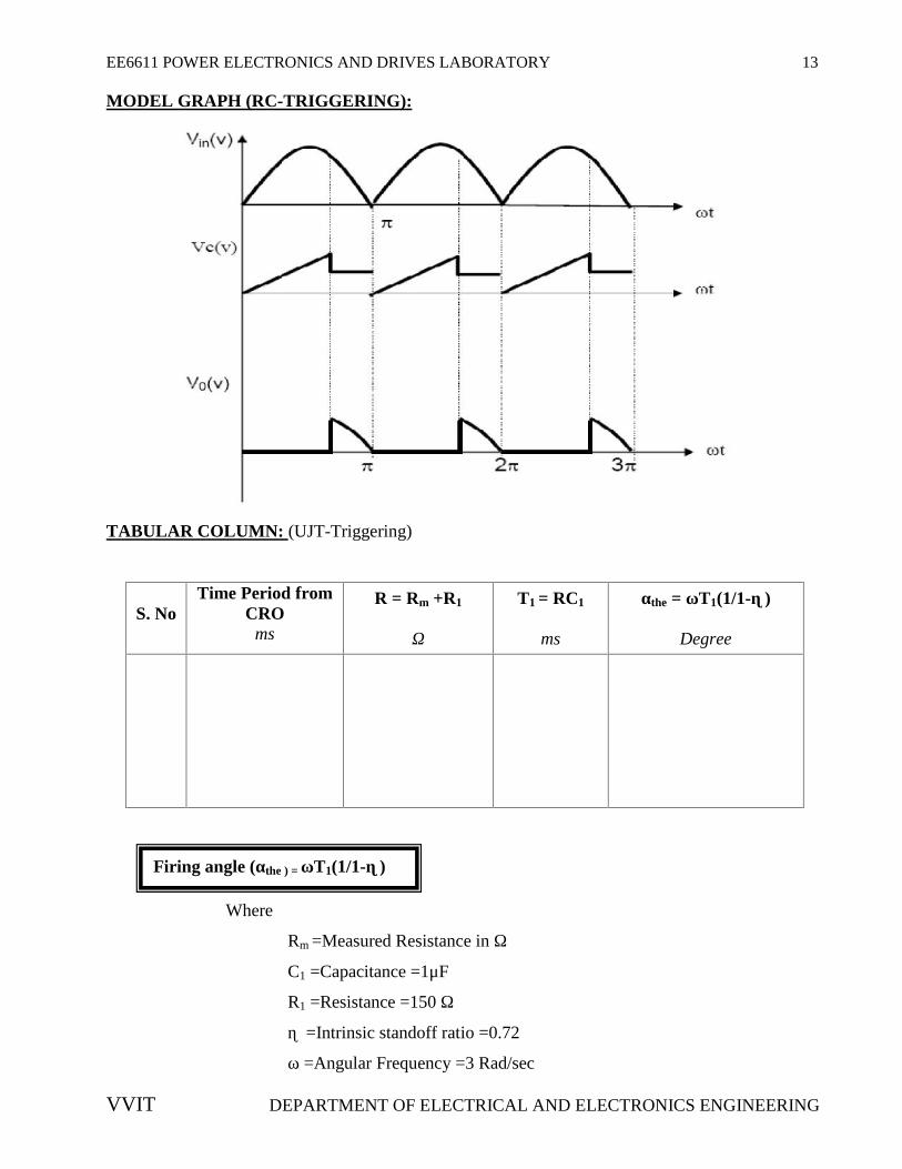
MODEL GRAPH (RC-TRIGGERING):
TABULAR COLUMN: (UJT-Triggering)
S. NoTime Period from
CROms
R = Rm +R1
Ω
T1 = RC1
ms
αthe = ωT1(1/1-ɳ)
Degree
Where
Rm =Measured Resistance in Ω
C1 =Capacitance =1μF
R1 =Resistance =150 Ω
ɳ =Intrinsic standoff ratio =0.72
ω =Angular Frequency =3 Rad/sec
Firing angle (αthe ) = ωT1(1/1-ɳ)

EE6611 POWER ELECTRONICS AND DRIVES LABORATORY 14
VVIT DEPARTMENT OF ELECTRICAL AND ELECTRONICS ENGINEERING
MODEL GRAPH ( UJT-TRIGGERING) :
RESULT:
Thus the R, RC &UJT triggering circuit for SCR was studied and its output waveforms were
plotted.

EE6611 POWER ELECTRONICS AND DRIVES LABORATORY 15
VVIT DEPARTMENT OF ELECTRICAL AND ELECTRONICS ENGINEERING
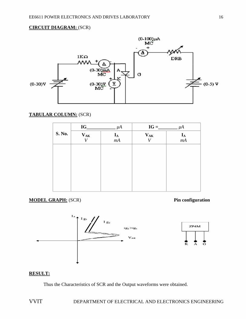
Ex. No: 2CHARACTERISTICS OF SCR
DATE:
AIM :To determine the characteristics of SCR and to study the operation of Single Phase Single
Pulse Converter using SCR.
APPARATUS REQUIRED:
S. No. APPARATUS RANGE TYPE QUANTITY
1 SCR CharacteristicsTrainer Kit
1
2 Voltmeter (0-30) V MC 1
3 Ammeter (0-30)mA MC 1
4 Ammeter (0-100)μA MC 1
5 CRO 30 MHZ 1
6 Patch Chords 10
PROCEDURE:
To determine the Characteristics of SCR
1) Make the connections as per the circuit diagram.
2) Switch on the supply
3) Set the gate current (IG) at a fixed value by varying RPS on the gate-cathode side.
4) Increase the voltage applied to anode-cathode side from zero until breakdown occurs.
5) Note down the breakdown voltage.
6) Draw the graph between anode to cathode voltage (VAK) and anode current (IA).
EE6611 POWER ELECTRONICS AND DRIVES LABORATORY 16
VVIT DEPARTMENT OF ELECTRICAL AND ELECTRONICS ENGINEERING
CIRCUIT DIAGRAM: (SCR)
TABULAR COLUMN: (SCR)
S. No.IG____________ μA IG =________ μAVAK
VIA
mAVAK
VIA
mA
MODEL GRAPH: (SCR) Pin configuration
RESULT:
Thus the Characteristics of SCR and the Output waveforms were obtained.

EE6611 POWER ELECTRONICS AND DRIVES LABORATORY 17
VVIT DEPARTMENT OF ELECTRICAL AND ELECTRONICS ENGINEERING
Ex. No: 3CHARACTERISTICS OF TRIAC
DATE:
AIM :
To determine the characteristics of TRIAC.
APPARATUS REQUIRED:
S. No. APPARATUS RANGE TYPE QUANTITY
1 TRIAC CharacteristicsTrainer Kit
LT-9002 1
2 Voltmeter (0-30) V MC 1
3 Ammeter (0-30)mA MC 1
4 Ammeter (0-50)mA MC 1
5 CRO 30 MHZ 1
6 Patch Chords 10
PROCEDURE:
1. Make the connections as per the circuit diagram.
2. Switch on the supply.
3. Set the gate current (IG) at a fixed value by varying RPS on the gate- cathode side.
4. Increase the voltage applied across anode and corresponding current is noted.
5. The above steps are repeated for different values of IG.
6. Draw the graph between anode to cathode voltage (VMT2) and anode Current (IMT2).
EE6611 POWER ELECTRONICS AND DRIVES LABORATORY 18
VVIT DEPARTMENT OF ELECTRICAL AND ELECTRONICS ENGINEERING
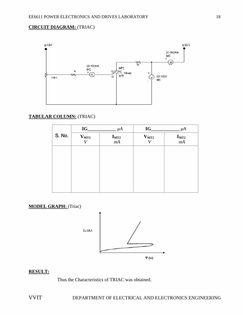
CIRCUIT DIAGRAM: (TRIAC)
TABULAR COLUMN: (TRIAC)
S. No.IG____________ μA IG____________ μA
VMT2
VIMT2
mAVMT2
VIMT2
mA
MODEL GRAPH: (Triac)
RESULT:
Thus the Characteristics of TRIAC was obtained.
EE6611 POWER ELECTRONICS AND DRIVES LABORATORY 18
VVIT DEPARTMENT OF ELECTRICAL AND ELECTRONICS ENGINEERING
CIRCUIT DIAGRAM: (TRIAC)
TABULAR COLUMN: (TRIAC)
S. No.IG____________ μA IG____________ μA
VMT2
VIMT2
mAVMT2
VIMT2
mA
MODEL GRAPH: (Triac)
RESULT:
Thus the Characteristics of TRIAC was obtained.

EE6611 POWER ELECTRONICS AND DRIVES LABORATORY 19
VVIT DEPARTMENT OF ELECTRICAL AND ELECTRONICS ENGINEERING
Ex. No: 4CHARACTERISTICS OF MOSFET & IGBTDATE:
AIM :
To determine the characteristics of MOSFET & IGBT.
APPARATUS REQUIRED:
S. No. APPARATUS RANGE TYPE QUANTITY
1MOSFET CharacteristicsTrainer Kit
LT-9002 1
2IGBT CharacteristicsTrainer Kit
1
3 Voltmeter (0-5) V MC 1
4 Voltmeter (0-30) V MC 1
5 Ammeter (0-5)mA MC 1
6 CRO 30 MHZ 1
7 Patch Chords 10
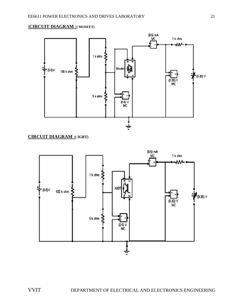
PROCEDURE: (MOSFET CHARACTERISTICS)
Drain characteristics:
1. Make the connection as per circuit diagram
2. Switch on the trainer
3. Gate- Source voltage (VGS) is kept at constant value by varying the gate bias voltage
4. Now slowly increase Drain- Source voltage (VDS) till MOSFET get turned on with the
indication that drain- source voltage decreases to it on state voltage drop
5. During this turn on period the load current is increased to higher value (28mA) and load
voltage is decreased to a minimum value (1V)
6. Note down the values of Drain – Source voltage (VDS) and drain current (ID)
7. For various Gate- Source voltage (VGS) take the different set of readings and tabulate it
8. Plot the graph between Drain- Source voltage (VDS) and Drain current (ID) for various gate
voltage

EE6611 POWER ELECTRONICS AND DRIVES LABORATORY 20
VVIT DEPARTMENT OF ELECTRICAL AND ELECTRONICS ENGINEERING
TRANSFER CHARACTERISTICS: (MOSFET)
1. Make the connection as per circuit diagram
2. Switch on the trainer
3. Drain- Source voltage (VDS) is kept constant value by varying the variable DC supply
4. Now slowly increase Gate- Source voltage (VGS) till MPOSFET get turned on with the
indication that drain current getting constant.
5. During this turn on period the current is increased to higher value (28mA) and load voltage is
decrease to a minimum value (1V)
6. During this turn OFF period the load current is minimum and load voltage is increased to
minimum value
7. Note down the value of Gate- Source voltage (VGS) and Drain current ID
8. For various Gate- Source voltage (VGS) take the different set of readings and tabulate it.
9. Plot the graph between Gate- Source voltage (VGS) and drain current ((ID) for various drain
voltages.
PROCEDURE: (IGBTCHARACTERISTICS)
Transfer Characteristics (IGBT)
1. Make the connection as per circuit diagram.
2. Connect the external (0-10V)DC meter to measure the gate voltage.
3. Connect the external (0-300 mA) DC,(0-30V) DC meter to measure the load current and load
voltage.
4. Keep the gate bias voltage potmeter in minimum position. Also maintain the load voltage as
in maximum.
5. Switch on the trainer.
6. Increase the gate voltage to 1V.
7. Vary the load voltage from minimum to maximum value.
8. Observe the load current and load voltage. The gate threshold voltage of IGBT is 2.5V.When
Vge is less than the threshold voltage the IGBT will not turn on. Therefore collector current
Ic is zero.
9. Slowly increase the gate voltage Vge simultaneously. Observe the load current (collector
current Ic ).
10. Further increasing of Vge at one particular voltage, the Ic will flow suddenly to a high value
which is called threshold voltage VGET.
EE6611 POWER ELECTRONICS AND DRIVES LABORATORY 21
VVIT DEPARTMENT OF ELECTRICAL AND ELECTRONICS ENGINEERING
\CIRCUIT DIAGRAM :( MOSFET)
CIRCUIT DIAGRAM :( IGBT)
EE6611 POWER ELECTRONICS AND DRIVES LABORATORY 21
VVIT DEPARTMENT OF ELECTRICAL AND ELECTRONICS ENGINEERING
\CIRCUIT DIAGRAM :( MOSFET)
CIRCUIT DIAGRAM :( IGBT)
EE6611 POWER ELECTRONICS AND DRIVES LABORATORY 21
VVIT DEPARTMENT OF ELECTRICAL AND ELECTRONICS ENGINEERING
\CIRCUIT DIAGRAM :( MOSFET)
CIRCUIT DIAGRAM :( IGBT)
EE6611 POWER ELECTRONICS AND DRIVES LABORATORY 22
VVIT DEPARTMENT OF ELECTRICAL AND ELECTRONICS ENGINEERING
TABULAR COLUMN (MOSFET):
Transfer Characteristics:
S. No.VDS1= -------------VVGS
mVID
mA
Drain Characteristics:
S. No V GS1 = ------------V
VDS
mV
ID
mA
MODEL GRAPH ( MOSFET ):
Transfer Characteristics Drain Characteristics

EE6611 POWER ELECTRONICS AND DRIVES LABORATORY 23
VVIT DEPARTMENT OF ELECTRICAL AND ELECTRONICS ENGINEERING
TABULAR COLUMN (IGBT)
Transfer Characteristics:
S. No.VGE = ------------- V VGE = ------------ VVCE
mVIC
mAVCE
mVIC
mA
Drain Characteristics:
S. No V CE = -------------- V
VGE
mV
IC
mA
MODEL GRAPH (IGBT):
V-I Characteristics Transfer Characteristics

EE6611 POWER ELECTRONICS AND DRIVES LABORATORY 24
VVIT DEPARTMENT OF ELECTRICAL AND ELECTRONICS ENGINEERING
V-I Characteristics (IGBT)
1. Make the connection as per circuit diagram.
2. Connect the external (0-10V) DC meter to measure the gate voltage.
3. Connect the external (0-300 mA) DC, (0-30V) DC meter to measure the load current and
load voltage.
4. Keep the gate bias voltage and load voltage as minimum.
5. Switch on the trainer.
6. Set the gate bias voltage VGE to threshold value.
7. Now slowly increase the collector emitter voltage VGE (Load voltage).
8. For each increment of VCE note down the collector current. At one particular value of VCE IC
remains constant value further increasing of VCE.
9. Decrease the load voltage VCE to minimum value and set the (VGE) gate bias to very small
increment of threshold.
10. Repeat the above experiment note down the IC and VCE.
11. Plot the VI characteristics of given IGBT was placed at different VGE.
RESULT:
Thus the Characteristics of MOSFET & IGBT were obtained.
EE6611 POWER ELECTRONICS AND DRIVES LABORATORY 25
VVIT DEPARTMENT OF ELECTRICAL AND ELECTRONICS ENGINEERING
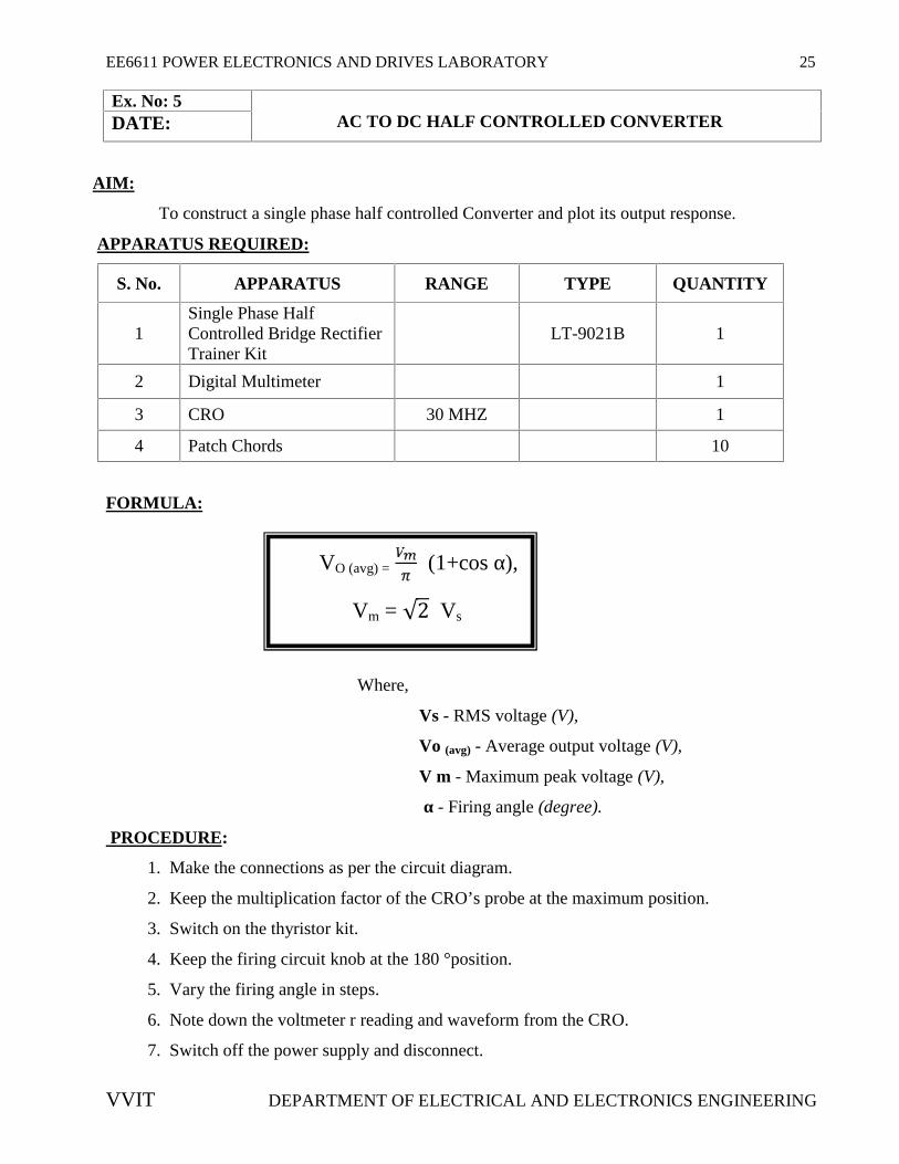
Ex. No: 5AC TO DC HALF CONTROLLED CONVERTERDATE:
AIM:
To construct a single phase half controlled Converter and plot its output response.
APPARATUS REQUIRED:
S. No. APPARATUS RANGE TYPE QUANTITY
1Single Phase HalfControlled Bridge RectifierTrainer Kit
LT-9021B 1
2 Digital Multimeter 1
3 CRO 30 MHZ 1
4 Patch Chords 10
FORMULA:
Where,
Vs - RMS voltage (V),
Vo (avg) - Average output voltage (V),
V m - Maximum peak voltage (V),
α - Firing angle (degree).
PROCEDURE:
1. Make the connections as per the circuit diagram.
2. Keep the multiplication factor of the CRO’s probe at the maximum position.
3. Switch on the thyristor kit.
4. Keep the firing circuit knob at the 180 °position.
5. Vary the firing angle in steps.
6. Note down the voltmeter r reading and waveform from the CRO.
7. Switch off the power supply and disconnect.
VO (avg) = (1+cos α),
Vm = √2 Vs
EE6611 POWER ELECTRONICS AND DRIVES LABORATORY 26
VVIT DEPARTMENT OF ELECTRICAL AND ELECTRONICS ENGINEERING
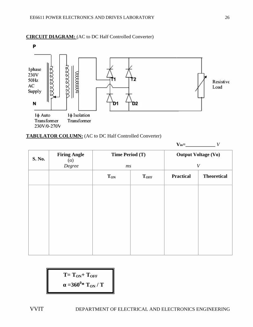
CIRCUIT DIAGRAM: (AC to DC Half Controlled Converter)
TABULATOR COLUMN: (AC to DC Half Controlled Converter)
Vin=____________ V
S. No.Firing Angle
(α)Degree
Time Period (T)
ms
Output Voltage (Vo)
V
TON TOFF Practical Theoretical
T= TON+ TOFF
α =3600* TON / T
EE6611 POWER ELECTRONICS AND DRIVES LABORATORY 26
VVIT DEPARTMENT OF ELECTRICAL AND ELECTRONICS ENGINEERING
CIRCUIT DIAGRAM: (AC to DC Half Controlled Converter)
TABULATOR COLUMN: (AC to DC Half Controlled Converter)
Vin=____________ V
S. No.Firing Angle
(α)Degree
Time Period (T)
ms
Output Voltage (Vo)
V
TON TOFF Practical Theoretical
T= TON+ TOFF
α =3600* TON / T
EE6611 POWER ELECTRONICS AND DRIVES LABORATORY 27
VVIT DEPARTMENT OF ELECTRICAL AND ELECTRONICS ENGINEERING
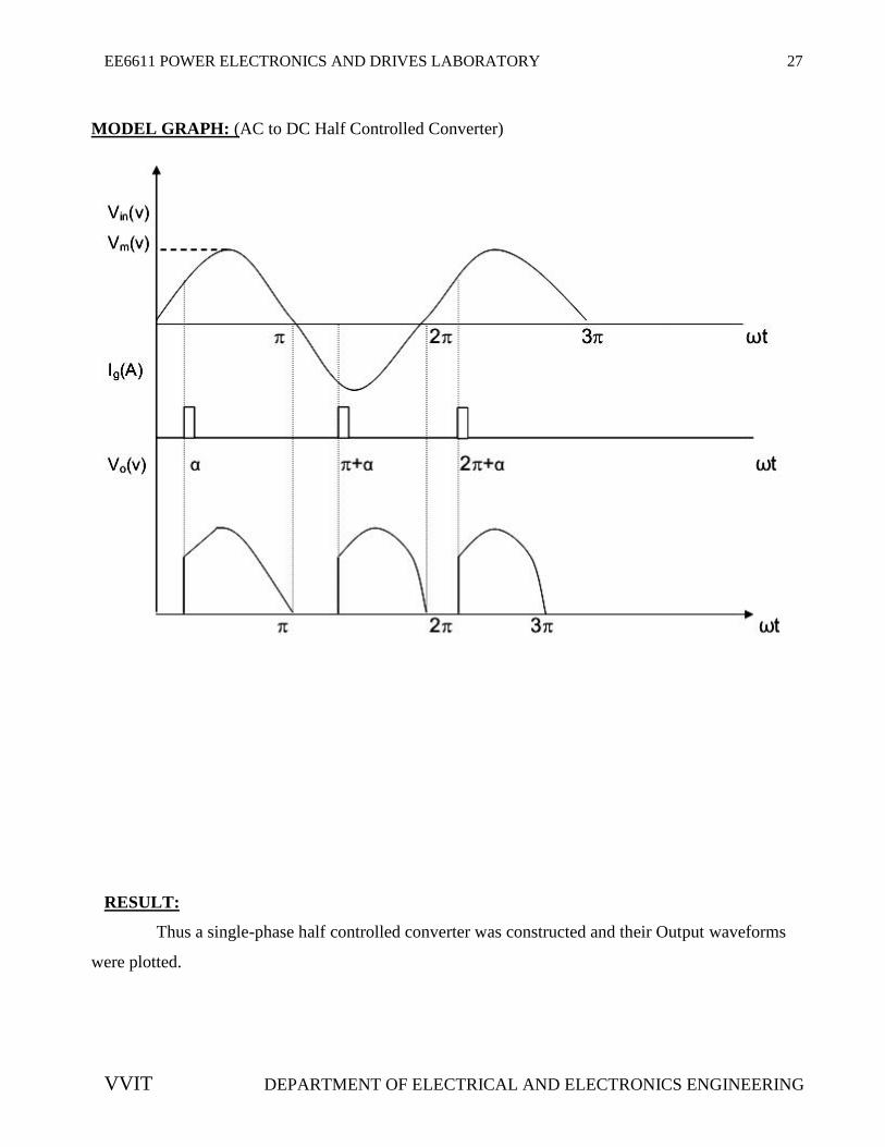
MODEL GRAPH: (AC to DC Half Controlled Converter)
RESULT:
Thus a single-phase half controlled converter was constructed and their Output waveforms
were plotted.
EE6611 POWER ELECTRONICS AND DRIVES LABORATORY 27
VVIT DEPARTMENT OF ELECTRICAL AND ELECTRONICS ENGINEERING
MODEL GRAPH: (AC to DC Half Controlled Converter)
RESULT:
Thus a single-phase half controlled converter was constructed and their Output waveforms
were plotted.
EE6611 POWER ELECTRONICS AND DRIVES LABORATORY 27
VVIT DEPARTMENT OF ELECTRICAL AND ELECTRONICS ENGINEERING
MODEL GRAPH: (AC to DC Half Controlled Converter)
RESULT:
Thus a single-phase half controlled converter was constructed and their Output waveforms
were plotted.

EE6611 POWER ELECTRONICS AND DRIVES LABORATORY 28
VVIT DEPARTMENT OF ELECTRICAL AND ELECTRONICS ENGINEERING
Ex. No :6AC TO DC FULLY CONTROLLED CONVERTERDATE:
AIM:
To construct a single phase fully controlled Converter and plot its response.
APPARATUS REQUIRED:
S. No. APPARATUS RANGE TYPE QUANTITY
1Single Phase FullyControlled Bridge RectifierTrainer Kit
LT-9020B 1
2 Digital Multimeter 1
3 CRO 30 MHZ 1
4 Patch Chords 10
FORMULA :
Where,
Vs - Rms voltage (V),
Vo(avg) - Average output voltage (V),
Vm - Maximum peak voltage (V),
α - Firing angle (degree).
PROCEDURE:
1. Make the connections as per the circuit diagram.
2. Keep the multiplication factor of the CRO’s probe at the maximum position.
3. Switch on the thyristor kit and firing circuit kit.
4. Keep the firing circuit knob at the 180 ° position.
5. Vary the firing angle in steps.
6. Note down the voltmeter reading and waveform from the CRO.
7. Switch off the power supply and disconnect.
VO (avg) = (1+cos α),
EE6611 POWER ELECTRONICS AND DRIVES LABORATORY 29
VVIT DEPARTMENT OF ELECTRICAL AND ELECTRONICS ENGINEERING
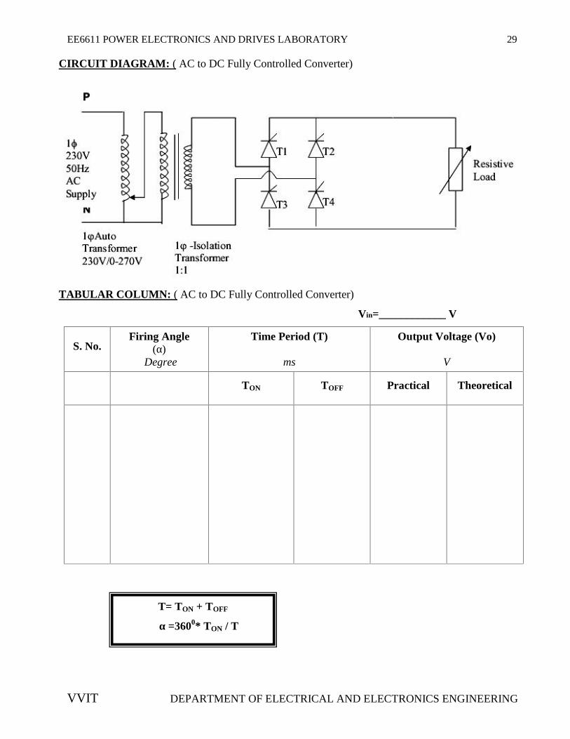
CIRCUIT DIAGRAM: ( AC to DC Fully Controlled Converter)
TABULAR COLUMN: ( AC to DC Fully Controlled Converter)
Vin=____________ V
S. No.Firing Angle
(α)Degree
Time Period (T)
ms
Output Voltage (Vo)
V
TON TOFF Practical Theoretical
T= TON + TOFF
α =3600* TON / T
EE6611 POWER ELECTRONICS AND DRIVES LABORATORY 29
VVIT DEPARTMENT OF ELECTRICAL AND ELECTRONICS ENGINEERING
CIRCUIT DIAGRAM: ( AC to DC Fully Controlled Converter)
TABULAR COLUMN: ( AC to DC Fully Controlled Converter)
Vin=____________ V
S. No.Firing Angle
(α)Degree
Time Period (T)
ms
Output Voltage (Vo)
V
TON TOFF Practical Theoretical
T= TON + TOFF
α =3600* TON / T

EE6611 POWER ELECTRONICS AND DRIVES LABORATORY 30
VVIT DEPARTMENT OF ELECTRICAL AND ELECTRONICS ENGINEERING
MODEL GRAPH: (AC to DC Fully Controlled Converter)
RESULT:
Thus a single-phase fully controlled converter was constructed and their responses were
plotted.
EE6611 POWER ELECTRONICS AND DRIVES LABORATORY 30
VVIT DEPARTMENT OF ELECTRICAL AND ELECTRONICS ENGINEERING
MODEL GRAPH: (AC to DC Fully Controlled Converter)
RESULT:
Thus a single-phase fully controlled converter was constructed and their responses were
plotted.
EE6611 POWER ELECTRONICS AND DRIVES LABORATORY 30
VVIT DEPARTMENT OF ELECTRICAL AND ELECTRONICS ENGINEERING
MODEL GRAPH: (AC to DC Fully Controlled Converter)
RESULT:
Thus a single-phase fully controlled converter was constructed and their responses were
plotted.

EE6611 POWER ELECTRONICS AND DRIVES LABORATORY 31
VVIT DEPARTMENT OF ELECTRICAL AND ELECTRONICS ENGINEERING
Ex. No : 7STEP UP AND STEP DOWN MO SFET BASED CHOPPERSDATE:
AIM:
To construct Step down & Step up MOSFET based choppers and to draw its Output
response.
APPARATUS REQUIRED:
S. No. APPARATUS RANGE TYPE QUANTITY
1Step up & Step downMOSFETbased chopper kit
VSMPS-07A 1
2 Digital Multimeter 1
3 CRO 30 MHZ 1
4 Patch Chords 10
PROCEDURE (STEP UP CHOPPER & STEP DOWN CHOPPER) :
1. Initially keep all the switches in the OFF position
2. Initially keep duty cycle POT in minimum position
3. Connect banana connector 24V DC source to 24V DC input.
4. Connect the driver pulse [output to MOSFET input.
5. Switch on the main supply.
6. Check the test point wave forms with respect to ground.
7. Vary the duty cycle POT and tabulate the Ton, Toff & output voltage
8. Trace the waveforms of Vo Vs & Io.
9. Draw the graph for Vo Vs Duty cycle, K

EE6611 POWER ELECTRONICS AND DRIVES LABORATORY 32
VVIT DEPARTMENT OF ELECTRICAL AND ELECTRONICS ENGINEERING
CIRCUIT DIAGRAM: (Step Up Chopper)
CIRCUIT DIAGRAM: (Step Down Chopper)
EE6611 POWER ELECTRONICS AND DRIVES LABORATORY 33
VVIT DEPARTMENT OF ELECTRICAL AND ELECTRONICS ENGINEERING
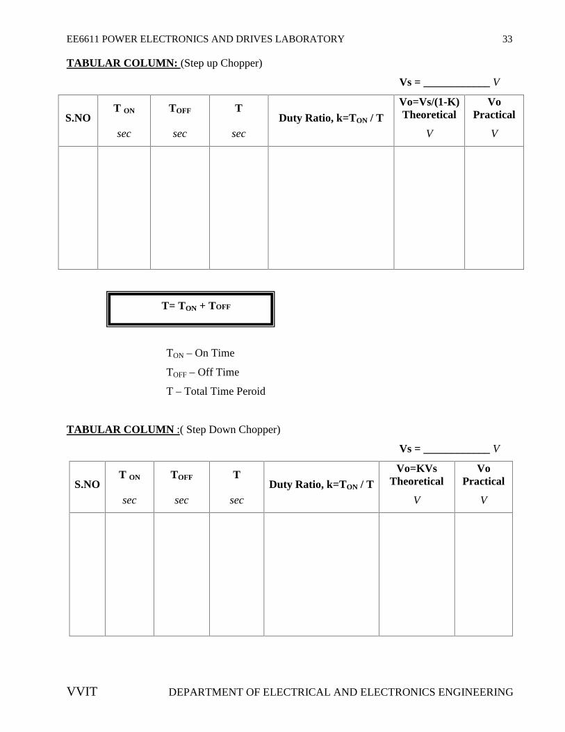
TABULAR COLUMN: (Step up Chopper)
Vs = ____________ V
S.NOT ON
sec
TOFF
sec
T
secDuty Ratio, k=TON / T
Vo=Vs/(1-K)Theoretical
V
VoPractical
V
TON – On Time
TOFF – Off Time
T – Total Time Peroid
TABULAR COLUMN :( Step Down Chopper)
Vs = ____________ V
S.NOT ON
sec
TOFF
sec
T
secDuty Ratio, k=TON / T
Vo=KVsTheoretical
V
VoPractical
V
T= TON + TOFF
EE6611 POWER ELECTRONICS AND DRIVES LABORATORY 34
VVIT DEPARTMENT OF ELECTRICAL AND ELECTRONICS ENGINEERING
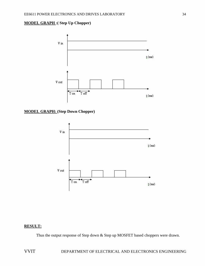
MODEL GRAPH :( Step Up Chopper)
MODEL GRAPH: (Step Down Chopper)
RESULT:
Thus the output response of Step down & Step up MOSFET based choppers were drawn.
EE6611 POWER ELECTRONICS AND DRIVES LABORATORY 34
VVIT DEPARTMENT OF ELECTRICAL AND ELECTRONICS ENGINEERING
MODEL GRAPH :( Step Up Chopper)
MODEL GRAPH: (Step Down Chopper)
RESULT:
Thus the output response of Step down & Step up MOSFET based choppers were drawn.
EE6611 POWER ELECTRONICS AND DRIVES LABORATORY 34
VVIT DEPARTMENT OF ELECTRICAL AND ELECTRONICS ENGINEERING
MODEL GRAPH :( Step Up Chopper)
MODEL GRAPH: (Step Down Chopper)
RESULT:
Thus the output response of Step down & Step up MOSFET based choppers were drawn.

EE6611 POWER ELECTRONICS AND DRIVES LABORATORY 35
VVIT DEPARTMENT OF ELECTRICAL AND ELECTRONICS ENGINEERING
CYCLE II
8. IGBT based single phase PWM inverter
9. IGBT based three phase PWM inverter
10. AC Voltage controller
11. Switched mode power converter.
12. Simulation of PE circuits (1 Φ&3Φ semi converter, 1 Φ&3Φfullconverter, dc-dc
Converters, ac voltage controllers).

EE6611 POWER ELECTRONICS AND DRIVES LABORATORY 36
VVIT DEPARTMENT OF ELECTRICAL AND ELECTRONICS ENGINEERING
Ex. No : 8IGBT BASED SINGLE PHASE PWM INVERTER
DATE:
AIM:
To obtain Single phase output wave forms for IGBT based PWM inverter
APPARATUS REQUIRED:
S. No. APPARATUS RANGE TYPE QUANTITY
1 IGBT Power Module Kit PEC16M3 1
2Single Phase PWM InverterControl Module
PEC16M4#1 1
3 CRO 30 MHZ 1
4 Load Rheostat 100Ω/5A 1
5 Patch Chords 10
PROCEDURE:
1. Make the connection as per the circuit diagram.
2. Connect the gating signal from the inverter module.
3. Switch ON D.C 24 V.
4. Keep the frequency knob to particulars frequency.
5. Observe the rectangular and triangular carrier waveforms on the CRO.
6. Obtain the output waveform across the load Rheostat.
EE6611 POWER ELECTRONICS AND DRIVES LABORATORY 37
VVIT DEPARTMENT OF ELECTRICAL AND ELECTRONICS ENGINEERING
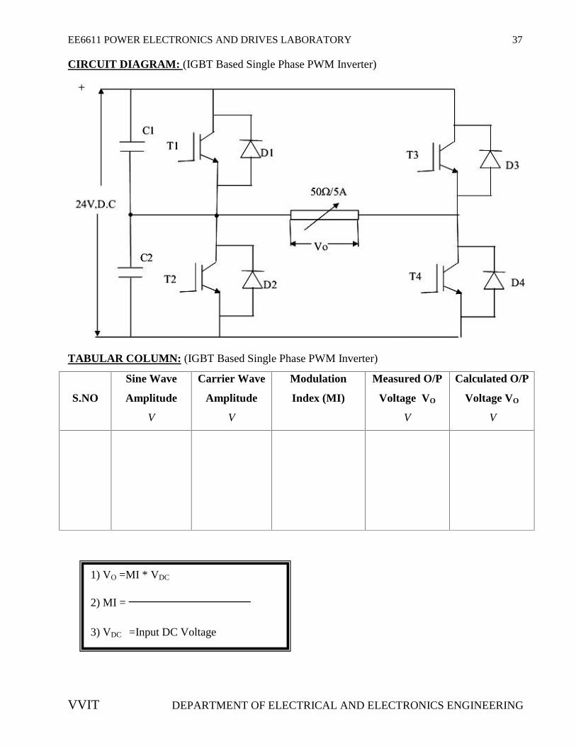
CIRCUIT DIAGRAM: (IGBT Based Single Phase PWM Inverter)
TABULAR COLUMN: (IGBT Based Single Phase PWM Inverter)
S.NO
Sine Wave
Amplitude
V
Carrier Wave
Amplitude
V
Modulation
Index (MI)
Measured O/P
Voltage VO
V
Calculated O/P
Voltage VO
V
1) VO =MI * VDC
2) MI =
3) VDC =Input DC Voltage
EE6611 POWER ELECTRONICS AND DRIVES LABORATORY 37
VVIT DEPARTMENT OF ELECTRICAL AND ELECTRONICS ENGINEERING
CIRCUIT DIAGRAM: (IGBT Based Single Phase PWM Inverter)
TABULAR COLUMN: (IGBT Based Single Phase PWM Inverter)
S.NO
Sine Wave
Amplitude
V
Carrier Wave
Amplitude
V
Modulation
Index (MI)
Measured O/P
Voltage VO
V
Calculated O/P
Voltage VO
V
1) VO =MI * VDC
2) MI =
3) VDC =Input DC Voltage

EE6611 POWER ELECTRONICS AND DRIVES LABORATORY 38
VVIT DEPARTMENT OF ELECTRICAL AND ELECTRONICS ENGINEERING
MODEL GRAPH: (IGBT Based Single Phase PWM Inverter)
RESULT:
Thus the output waveform for IGBT inverter (PWM) was obtained.
EE6611 POWER ELECTRONICS AND DRIVES LABORATORY 38
VVIT DEPARTMENT OF ELECTRICAL AND ELECTRONICS ENGINEERING
MODEL GRAPH: (IGBT Based Single Phase PWM Inverter)
RESULT:
Thus the output waveform for IGBT inverter (PWM) was obtained.
EE6611 POWER ELECTRONICS AND DRIVES LABORATORY 38
VVIT DEPARTMENT OF ELECTRICAL AND ELECTRONICS ENGINEERING
MODEL GRAPH: (IGBT Based Single Phase PWM Inverter)
RESULT:
Thus the output waveform for IGBT inverter (PWM) was obtained.
EE6611 POWER ELECTRONICS AND DRIVES LABORATORY 39
VVIT DEPARTMENT OF ELECTRICAL AND ELECTRONICS ENGINEERING
Ex. No: 9IGBT BASED THREE PHASE PWM INVERTER
DATE:
AIM:
To study the three phase inverter operation by using sine, trapezoidal square PWM.
APPARATUS REQUIRED:
S. No. APPARATUS RANGE TYPE QUANTITY
1 IGBT Power Module Kit VPET-106A 1
2Chopper/Inverter PWMControl Module
PEC16HV2B 1
3 CRO 30 MHZ 1
4 Patch Chords 10
CONNECTION PROCEDURE:
1. Connect 1 Phase AC input supply to the power module.
2. Connect the power module and controller module to the supply mains.
3. Connect PWM output of the controller module to the PWM input of the power module using
a 9 pin to 15 pin cable.
4. Connect the power module to R&L load.
5. Connect motor speed feedback cable to the motor feedback input of the controller module.
EXPERIMENTAL PROCEDURE:
1. Verify the connections as per the connection procedure.
2. Switch ON the power ON/OFF switch in both the IGBT based power module and the
controller module.
3. Switch ON the MCB in the power module.
4. When the module is switched ON select 3 phase inverter by using decrement key.
5. Then select sine PWM by using increment switch.
6. Vary the frequency value by using increment and decrement key and vary the amplitude
value by using enter key.
7. Repeat the above steps for trapezoidal PWM and square PWM.
EE6611 POWER ELECTRONICS AND DRIVES LABORATORY 40
VVIT DEPARTMENT OF ELECTRICAL AND ELECTRONICS ENGINEERING
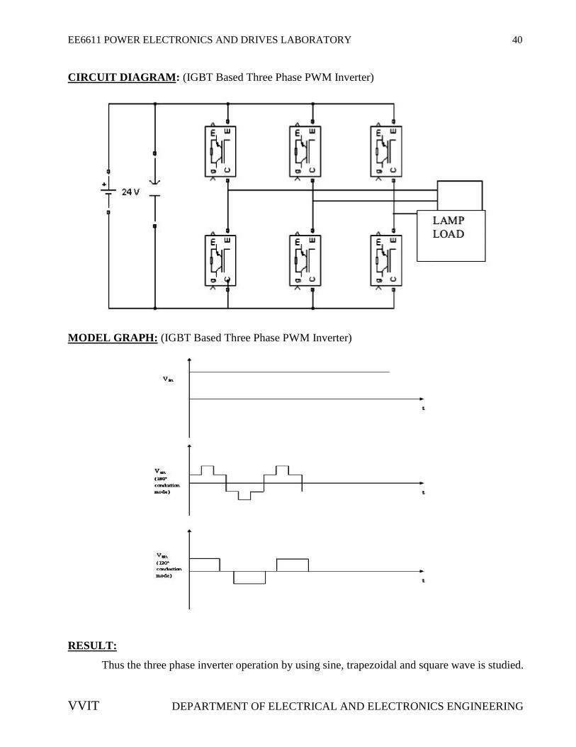
CIRCUIT DIAGRAM: (IGBT Based Three Phase PWM Inverter)
MODEL GRAPH: (IGBT Based Three Phase PWM Inverter)
RESULT:
Thus the three phase inverter operation by using sine, trapezoidal and square wave is studied.
EE6611 POWER ELECTRONICS AND DRIVES LABORATORY 40
VVIT DEPARTMENT OF ELECTRICAL AND ELECTRONICS ENGINEERING
CIRCUIT DIAGRAM: (IGBT Based Three Phase PWM Inverter)
MODEL GRAPH: (IGBT Based Three Phase PWM Inverter)
RESULT:
Thus the three phase inverter operation by using sine, trapezoidal and square wave is studied.
EE6611 POWER ELECTRONICS AND DRIVES LABORATORY 41
VVIT DEPARTMENT OF ELECTRICAL AND ELECTRONICS ENGINEERING
Ex. No:10SINGLE PHASE AC VOLTAGE CONTROLLER USING TRIAC
DATE:
AIM:
To study the Single phase AC voltage control using TRIAC with DIAC or UJT Firing
Circuit.
APPARATUS REQUIRED:
S. No. APPARATUS RANGE TYPE QUANTITY
1AC Regulator using SCR&TRIAC
LT-9025 1
2 CRO 30 MHZ 1
3 Patch Chords 10
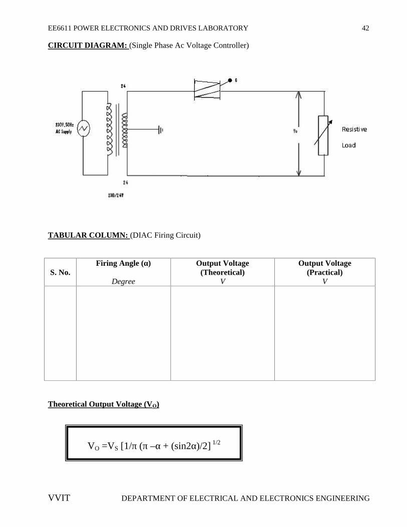
CIRCUIT OPERATION:
1. When potentiometer is in minimum position drop across potentiometer is zero and hence
maximum voltage is available across capacitor. This Vc shorts the diac (Vc > Vbo) and
triggers the triac turning triac to ON – state there lamp glows with Maximum intensity.
2. When the potentiometer is in maximum position voltage drop across Potentiometer is
maximum. Hence minimum voltage is available across capacitor (Vc M Vbo) hence triac
to is not triggered hence lamp does not glow.
3. When potentiometer is in medium position a small voltage is available across Capacitor
hence lamp glows with minimum intensity.
PROCEDURE:
1. Connections are given as per the circuit diagram.
2. Keep ramp control potmeter in minimum position.
3. Switch ON the trainer.
4. Observe the variation in output voltage for different firing angles through voltmeter.
5. Calculate the output voltage theoretically.
EE6611 POWER ELECTRONICS AND DRIVES LABORATORY 42
VVIT DEPARTMENT OF ELECTRICAL AND ELECTRONICS ENGINEERING
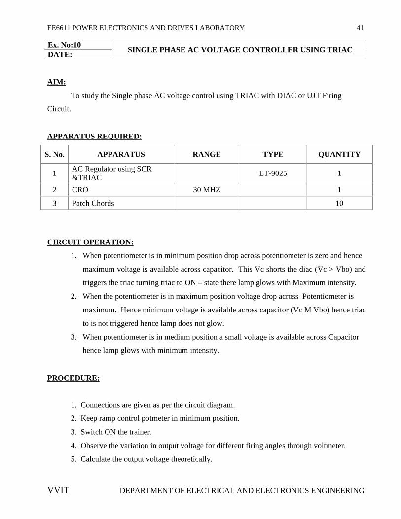
CIRCUIT DIAGRAM: (Single Phase Ac Voltage Controller)
TABULAR COLUMN: (DIAC Firing Circuit)
S. No.Firing Angle (α)
Degree
Output Voltage(Theoretical)
V
Output Voltage(Practical)
V
Theoretical Output Voltage (VO)
VO =VS [1/π (π –α + (sin2α)/2] 1/2
EE6611 POWER ELECTRONICS AND DRIVES LABORATORY 42
VVIT DEPARTMENT OF ELECTRICAL AND ELECTRONICS ENGINEERING
CIRCUIT DIAGRAM: (Single Phase Ac Voltage Controller)
TABULAR COLUMN: (DIAC Firing Circuit)
S. No.Firing Angle (α)
Degree
Output Voltage(Theoretical)
V
Output Voltage(Practical)
V
Theoretical Output Voltage (VO)
VO =VS [1/π (π –α + (sin2α)/2] 1/2
EE6611 POWER ELECTRONICS AND DRIVES LABORATORY 43
VVIT DEPARTMENT OF ELECTRICAL AND ELECTRONICS ENGINEERING
MODEL GRAPH: ( Single Phase Ac Voltage Controller)
RESULT:
Thus the operation and performance of t he single phase AC voltage control using TRIAC is
done and output Verified
EE6611 POWER ELECTRONICS AND DRIVES LABORATORY 44
VVIT DEPARTMENT OF ELECTRICAL AND ELECTRONICS ENGINEERING
Ex. No:11SWITCHED MODE POWER CONVERTER
DATE:
AIM:
To study the switched mode power Converter and to plot its output waveforms.
APPARATUS REQUIRED:
S. No. APPARATUS RANGE TYPE QUANTITY
1Switched mode powerconverter kit
1
2 Lamp load 1
3 CRO 30 MHZ 1
4 Patch Chords 10
PROCEDURE:
1. Plug in the unit to AC mains 230V, 50Hz supply.
2. Switch ON the toggle switch. The neon lamp will glow indicating that the unit is ready.
3. LED in the AC source will be glowing indicating the availability of AC 20V.
4. Observe the trigger circuit waveforms.
5. Connect the AC source to the power circuit using patch chords.
6. Connect the lamp load with incandescent lamp of 36V.
7. Observe the load output for a chosen setting of duty cycle setting.
8. Output will be DC in the range of 0 to 40V.
.
EE6611 POWER ELECTRONICS AND DRIVES LABORATORY 45
VVIT DEPARTMENT OF ELECTRICAL AND ELECTRONICS ENGINEERING
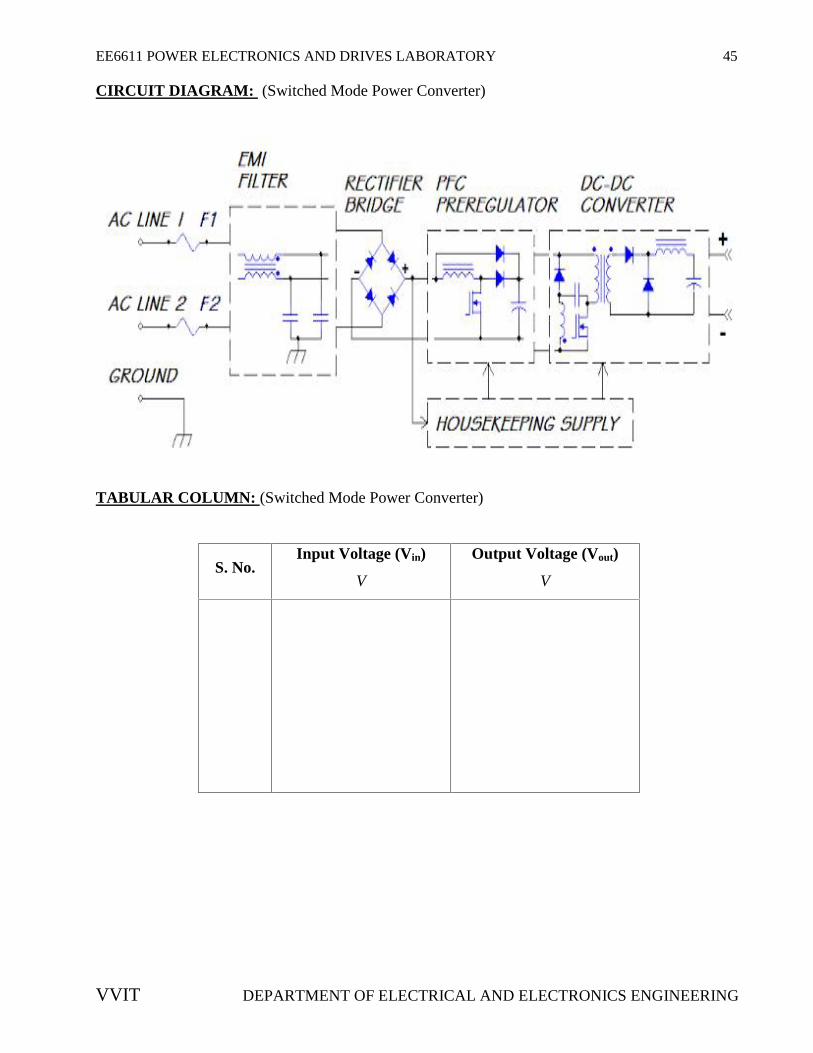
CIRCUIT DIAGRAM: (Switched Mode Power Converter)
TABULAR COLUMN: (Switched Mode Power Converter)
S. No.Input Voltage (Vin)
V
Output Voltage (Vout)
V
EE6611 POWER ELECTRONICS AND DRIVES LABORATORY 46
VVIT DEPARTMENT OF ELECTRICAL AND ELECTRONICS ENGINEERING
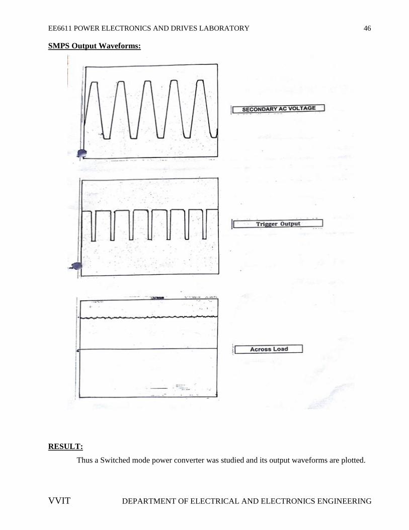
SMPS Output Waveforms:
RESULT:
Thus a Switched mode power converter was studied and its output waveforms are plotted.

EE6611 POWER ELECTRONICS AND DRIVES LABORATORY 47
VVIT DEPARTMENT OF ELECTRICAL AND ELECTRONICS ENGINEERING
SIMULATION OF POWER ELECTRONICS CIRCUITS
STUDY OF BASIC MATLAB COMMANDS:
The name MATLAB stands for MATRIX LABORATORY. MATLAB was originally
written to provide easy access to matrix software developed by the LINPACK and EISPACK
projects. Today, MATLAB engines incorporate the LAPACK and BLAS libraries, embedding the
state of the art in software for matrix computation. It has evolved over a period of years with input
from many users. In university environments, it is the standard instructional tool for introductory and
advanced courses in MATHEMATICS, ENGINEERING AND SCIENCE. In industry, MATLAB is
the tool of choice for high-productivity research, development, and analysis.
MATLAB is a high-performance language for technical computing. It integrates computation,
visualization, and programming in an easy-to-use environment where problems and solutions are
expressed in familiar mathematical notation. Typical uses include,
Math and computation
Algorithm development
Data acquisition Modeling, simulation, and prototyping
Data analysis, exploration, and visualization Scientific and engineering graphics
Application development, including graphical user interface building.
It is an interactive system whose basic data element is an array that does not require dimensioning.
This allows you to solve many technical computing problems, especially those with matrix and
vector formulations, in a fraction of the time it would take to write a program in a scalar non-
interactive language such as C or FORTRAN. It also features a family of add-on application-
specific solutions called toolboxes. Very important to most users of MATLAB, toolboxes allow you
to learn and apply specialized technology. Toolboxes are comprehensive collections of MATLAB
functions (M-files) that extend the MATLAB environment to solve particular classes of problems.
Areas in which toolboxes are available include signal processing, control systems, neural networks,
fuzzy logic, wavelets, simulation, and many others.

EE6611 POWER ELECTRONICS AND DRIVES LABORATORY 48
VVIT DEPARTMENT OF ELECTRICAL AND ELECTRONICS ENGINEERING
Ex. No:12SIMULATION OF SINGLE PHASE SEMI CONVERTER
DATE:
AIM:
To simulate single Phase Semi Converter circuit with R load in MATLAB - Simulink.
APPARATUS REQUIRED:
A PC with MATLAB package.
THEORY:
A semi converter uses two diodes and two thyristors and there is a limited control
over the level of dc output voltage. A semi converter is one quadrant converter. A one-quadrant
converter has same polarity of dc output voltage and current at its output terminals and it is always
positive. It is also known as two - pulse converter. Figure shows half controlled rectifier with R
load. This circuit consists of two SCRs T1 and T2, two diodes D1 and D2. During the positive half
cycle of the ac supply, SCR T1 and diode D2 are forward biased when the SC R T1 is triggered at a
firing angle ω t = α, the SCR T1 and diode D2 comes to the on state. Now the load current flows
through the Path L - T1- R load –D2 - N. During this period, the output voltage and current are
positive. At ωt = π , the load voltage and load current reaches to zero, then SCR T1 and diode D2
comes to off state since supply voltage has been reversed. During the negative half cycle of the ac
supply, SCR T2 and diode D1 are forward biased.
When SCR T2 is triggered at a firing angle ωt = π + α, the SCR T2 and diode D1
comes to on state. Now the load current flows through the path N - T2- R load –D1 -L. During this
period, output voltage and output current will be positive. At ωt = 2π,the load voltage and load
current reaches to zero then S CR T2 and diode D1 comes to off state since the voltage has been
reversed. During the period [(π + α) to 2π] SCR T2and diode D1 are conducting.
VOUT = (√2VS) (1+COSα)
/π
EE6611 POWER ELECTRONICS AND DRIVES LABORATORY 49
VVIT DEPARTMENT OF ELECTRICAL AND ELECTRONICS ENGINEERING
PROCEDURE:
1. In MATLAB software open a new model in File->New->model.
2. Start SIMULINK library browser by clicking the symbol in toolbar.
3. And Open the libraries that contain the blocks you will need. These usually will
Include the sources, sinks, math and continuous function block and possibly other.
4. Drag the needed blocks from the library folders to that new untitled Simulink window. You must
give it a name using the Save As menu command under the file menu heading. The assigned
filename is automatically appended with an .mdl extension.
5. Arrange these blocks in orderly way corresponding by Matlab Model shown below.
6. Interconnect the blocks by dragging the cursor from the output of one block to the
Input of another block.
7. Double click on any block having parameters that must be established and set
these parameters.
8. It is necessary to specify a stop time for the simulation; this is done by clicking on
the simulation parameters entry on the simulation-> parameters entry on the Simulation toolbar.
9. Now we are ready to simulate our block diagram. Press start icon to start the Simulation. After
simulation is done, double click the scope block to display the Output. Click the auto scale icon
in the display window to scale the axis as per variable range.
10. Finally Save the Output.
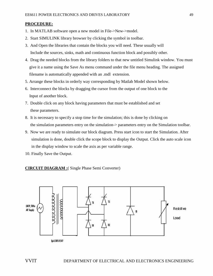
CIRCUIT DIAGRAM :( Single Phase Semi Converter)
EE6611 POWER ELECTRONICS AND DRIVES LABORATORY 49
VVIT DEPARTMENT OF ELECTRICAL AND ELECTRONICS ENGINEERING
PROCEDURE:
1. In MATLAB software open a new model in File->New->model.
2. Start SIMULINK library browser by clicking the symbol in toolbar.
3. And Open the libraries that contain the blocks you will need. These usually will
Include the sources, sinks, math and continuous function block and possibly other.
4. Drag the needed blocks from the library folders to that new untitled Simulink window. You must
give it a name using the Save As menu command under the file menu heading. The assigned
filename is automatically appended with an .mdl extension.
5. Arrange these blocks in orderly way corresponding by Matlab Model shown below.
6. Interconnect the blocks by dragging the cursor from the output of one block to the
Input of another block.
7. Double click on any block having parameters that must be established and set
these parameters.
8. It is necessary to specify a stop time for the simulation; this is done by clicking on
the simulation parameters entry on the simulation-> parameters entry on the Simulation toolbar.
9. Now we are ready to simulate our block diagram. Press start icon to start the Simulation. After
simulation is done, double click the scope block to display the Output. Click the auto scale icon
in the display window to scale the axis as per variable range.
10. Finally Save the Output.
CIRCUIT DIAGRAM :( Single Phase Semi Converter)
EE6611 POWER ELECTRONICS AND DRIVES LABORATORY 50
VVIT DEPARTMENT OF ELECTRICAL AND ELECTRONICS ENGINEERING
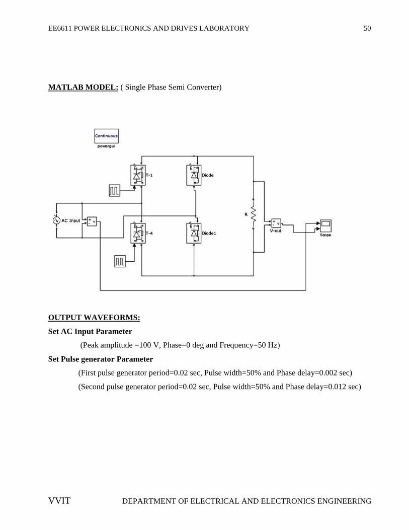
MATLAB MODEL: ( Single Phase Semi Converter)
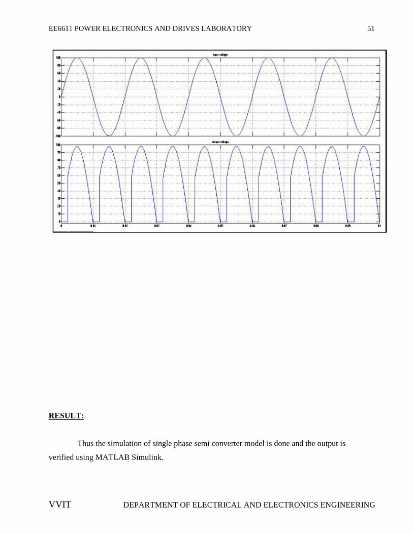
OUTPUT WAVEFORMS:
Set AC Input Parameter
(Peak amplitude =100 V, Phase=0 deg and Frequency=50 Hz)
Set Pulse generator Parameter
(First pulse generator period=0.02 sec, Pulse width=50% and Phase delay=0.002 sec)
(Second pulse generator period=0.02 sec, Pulse width=50% and Phase delay=0.012 sec)
EE6611 POWER ELECTRONICS AND DRIVES LABORATORY 50
VVIT DEPARTMENT OF ELECTRICAL AND ELECTRONICS ENGINEERING
MATLAB MODEL: ( Single Phase Semi Converter)
OUTPUT WAVEFORMS:
Set AC Input Parameter
(Peak amplitude =100 V, Phase=0 deg and Frequency=50 Hz)
Set Pulse generator Parameter
(First pulse generator period=0.02 sec, Pulse width=50% and Phase delay=0.002 sec)
(Second pulse generator period=0.02 sec, Pulse width=50% and Phase delay=0.012 sec)
EE6611 POWER ELECTRONICS AND DRIVES LABORATORY 51
VVIT DEPARTMENT OF ELECTRICAL AND ELECTRONICS ENGINEERING
RESULT:
Thus the simulation of single phase semi converter model is done and the output is
verified using MATLAB Simulink.
EE6611 POWER ELECTRONICS AND DRIVES LABORATORY 51
VVIT DEPARTMENT OF ELECTRICAL AND ELECTRONICS ENGINEERING
RESULT:
Thus the simulation of single phase semi converter model is done and the output is
verified using MATLAB Simulink.
EE6611 POWER ELECTRONICS AND DRIVES LABORATORY 51
VVIT DEPARTMENT OF ELECTRICAL AND ELECTRONICS ENGINEERING
RESULT:
Thus the simulation of single phase semi converter model is done and the output is
verified using MATLAB Simulink.

EE6611 POWER ELECTRONICS AND DRIVES LABORATORY 52
VVIT DEPARTMENT OF ELECTRICAL AND ELECTRONICS ENGINEERING
Ex. No.13SIMULATION OF SINGLE PHASE FULL CONVERTER
DATE:
AIM:
To simulate single Phase Full Converter circuit with R load in MATLAB - Simulink.
APPARATUS REQUIRED:
A PC with MATLAB package.
THEORY:
SINGLE PHASE FULL CONVERTER
A fully controlled converter or full converter uses thyristors only and there is a wider
control over the level of dc output voltage. With pure resistive load, it is single quadrant converter.
Here, both the output voltage and output current are positive. With RL- load it becomes a two
quadrant converter. Here, output voltage is either positive or negative but output current is always
positive. Figure shows the quadrant operation of fully controlled bridge rectifier with R- load. Fig
shows single phase fully controlled rectifier with resistive load. This type of full wave rectifier
circuit consists of four SCRs. During the positive half cycle, SCRs T1 and T2 are forward biased. At
ωt = α, SCRs T1 and T3 are triggered, and then the current flows through the L – T1- R load – T3 –
N. At ωt = π, supply voltage falls to zero and the current also goes to zero. Hence SCRs T1 and T3
turned off. During negative half cycle (π to 2π).SCRs T3 and T4 forward biased. At ωt = π + α,
SCRs T2 and T4 are triggered, then current flows through the path N – T2 – R load- T4 – L. At
ωt = 2π, supply voltage and current goes to zero, SCRs T2 and T4 are turned off.
The Fig-3, shows the current and voltage waveforms for this circuit. For large power dc
loads, 3-phase ac to dc converters are commonly used. The various types of three-phase phase-
controlled converters are 3 phase half-wave converter, 3-phase semi converter, 3-phase full
controlled and 3-phase dual converter. Three-phase half-wave converter is rarely used in industry
because it introduces dc component in the supply current. Semi converters and full converters are
quite common in industrial applications. A dual is used only when reversible dc drives with power
ratings of several MW are required. The advantages of three phase converters over single-phase
converters are as under: In 3-phase converters, the ripple frequency of the converter output voltage
is higher than in single-phase converter.

EE6611 POWER ELECTRONICS AND DRIVES LABORATORY 53
VVIT DEPARTMENT OF ELECTRICAL AND ELECTRONICS ENGINEERING
PROCEDURE:
1. In MATLAB software open a new model in File->New->model.
2. Start SIMULINK library browser by clicking the symbol in toolbar .
3. And Open the libraries that contain the blocks you will need . These usually will include the
sources, sinks, math and continuous function block and possibly other.
4. Drag the needed blocks from the library folders to that new untitled Simulink Window. You
must give it a name using the Save As menu command under the File menu heading. The
assigned filename is automatically appended with an .mdl Extension.
5. Arrange these blocks in orderly way corresponding by Matlab Model Shown Below.
6. Interconnect the blocks by dragging the cursor from the output of one block to the Input of
another block.
7. Double click on any block having parameters that must be established and set these
parameters.
8. It is necessary to specify a stop time for the simulation; this is done by clicking on the
simulation parameters entry on the simulation-> parameters entry on the Simulation toolbar.
9. Now we are ready to simulate our block diagram. Press start icon to start the Simulation.
after simulation is done, double click the scope block to display the Output. Click the auto
scale icon in the display window to scale the axis as per Variable range.
10. Finally Save the Output.
SINGLE PHASE FULL CONVERTER
EE6611 POWER ELECTRONICS AND DRIVES LABORATORY 54
VVIT DEPARTMENT OF ELECTRICAL AND ELECTRONICS ENGINEERING
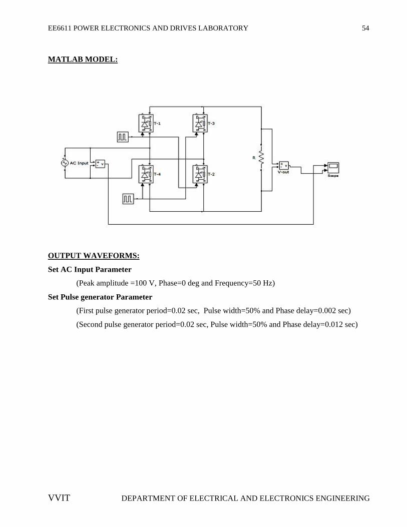
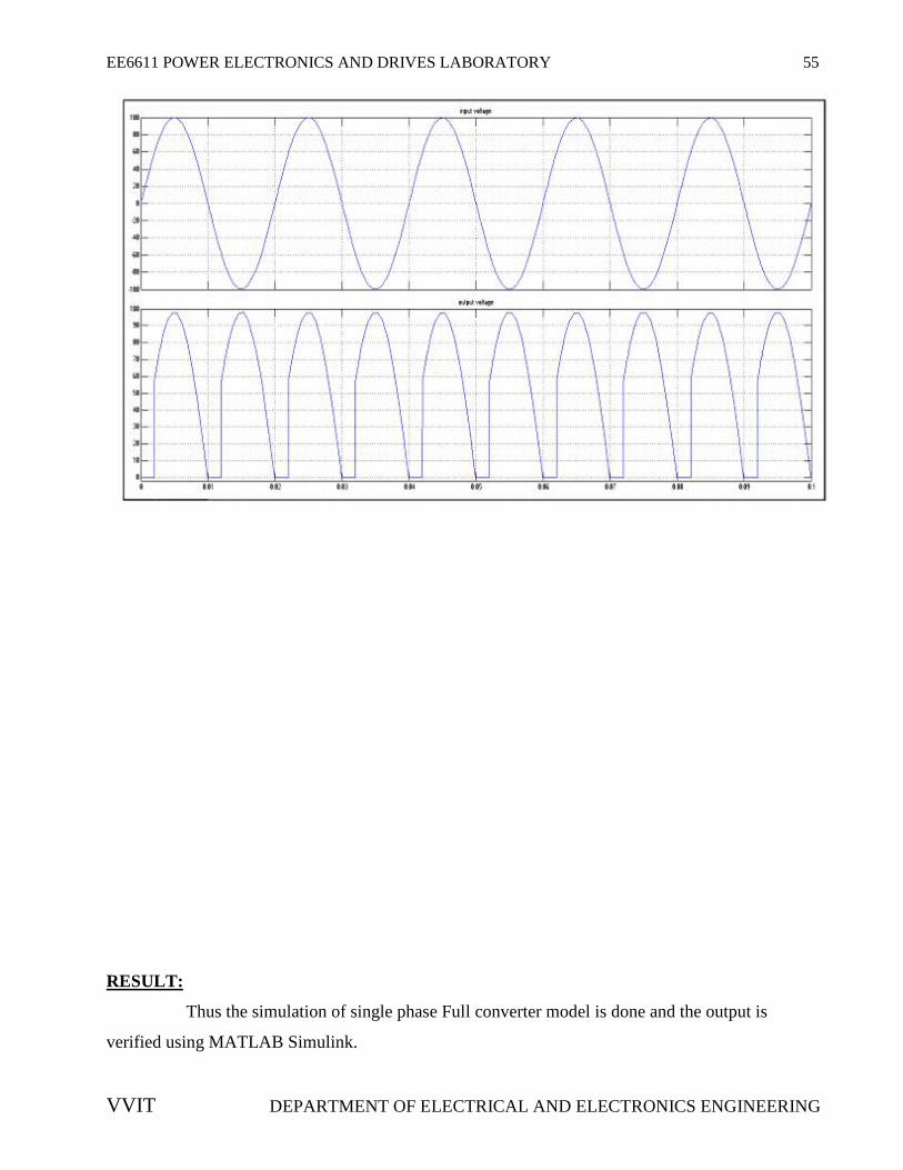
MATLAB MODEL:
OUTPUT WAVEFORMS:
Set AC Input Parameter
(Peak amplitude =100 V, Phase=0 deg and Frequency=50 Hz)
Set Pulse generator Parameter
(First pulse generator period=0.02 sec, Pulse width=50% and Phase delay=0.002 sec)
(Second pulse generator period=0.02 sec, Pulse width=50% and Phase delay=0.012 sec)
EE6611 POWER ELECTRONICS AND DRIVES LABORATORY 54
VVIT DEPARTMENT OF ELECTRICAL AND ELECTRONICS ENGINEERING
MATLAB MODEL:
OUTPUT WAVEFORMS:
Set AC Input Parameter
(Peak amplitude =100 V, Phase=0 deg and Frequency=50 Hz)
Set Pulse generator Parameter
(First pulse generator period=0.02 sec, Pulse width=50% and Phase delay=0.002 sec)
(Second pulse generator period=0.02 sec, Pulse width=50% and Phase delay=0.012 sec)
EE6611 POWER ELECTRONICS AND DRIVES LABORATORY 55
VVIT DEPARTMENT OF ELECTRICAL AND ELECTRONICS ENGINEERING
RESULT:
Thus the simulation of single phase Full converter model is done and the output is
verified using MATLAB Simulink.

EE6611 POWER ELECTRONICS AND DRIVES LABORATORY 56
VVIT DEPARTMENT OF ELECTRICAL AND ELECTRONICS ENGINEERING
Ex. No:14 SIMULATION OF SINGLE PHASE AC VOLTAGE CONTROL
USING TRIACDATE:
AIM:
To simulate single Phase AC Voltage Control Using TRIAC circuit with R load in
MATLAB - Simulink.
APPARATUS REQUIRED:
A PC with MATLAB package.
THEORY:
SINGLE PHASE AC VOLTAGE CONTROL USING TRIAC
Triac is a bidirectional thyristor with three terminals. Triac is the word derived by
Combining the capital letters from the words Triode and AC. In operation triac is equivalent to two
SCRs connected in anti- parallel. It is used extensively for the control of power in ac circuit as it can
conduct in both the direction. Its three terminals are MT1 (main terminal 1), MT2 (main terminal 2)
and G (gate).
PROCEDURE:
1. In MATLAB software open a new model in File->New->model.
2. Start SIMULINK library browser by clicking the symbol in toolbar .
3. And Open the libraries that contain the blocks you will need. These usually will
include the sources, sinks, math and continuous function block and possibly other.
4. Drag the needed blocks from the library folders to that new untitled Simulink
window. You must give it a name using the Save As menu command under the File
menu heading. The assigned filename is automatically appended with an .mdl
extension.
5. Arrange these blocks in orderly way corresponding by Matlab Model Shown Below.
6. Interconnect the blocks by dragging the cursor from the output of one block to the
input of another block.
7. Double click on any block having parameters that must be established and set these
parameters.

EE6611 POWER ELECTRONICS AND DRIVES LABORATORY 57
VVIT DEPARTMENT OF ELECTRICAL AND ELECTRONICS ENGINEERING
8. It is necessary to specify a stop time for the simulation; this is done by clicking on the
simulation parameters entry on the simulation-> parameters entry on the Simulation
toolbar.
9. Now we are ready to simulate our block diagram. Press start icon to start the
Simulation. After simulation is done, double click the scope block to display the
output. Click the auto scale icon in the display window to scale the axis as per
variable range.
10. Finally Save the Output.
SINGLE PHASE AC VOLTAGE CONTROL USING TRIAC:
MATLAB MODEL:
EE6611 POWER ELECTRONICS AND DRIVES LABORATORY 58
VVIT DEPARTMENT OF ELECTRICAL AND ELECTRONICS ENGINEERING
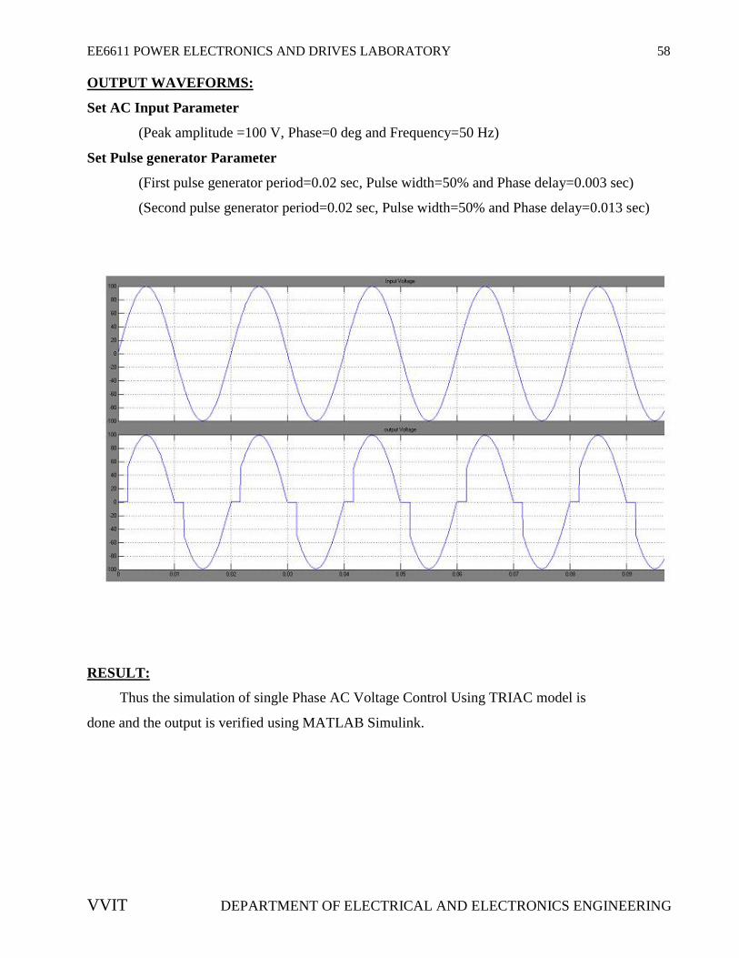
OUTPUT WAVEFORMS:
Set AC Input Parameter
(Peak amplitude =100 V, Phase=0 deg and Frequency=50 Hz)
Set Pulse generator Parameter
(First pulse generator period=0.02 sec, Pulse width=50% and Phase delay=0.003 sec)
(Second pulse generator period=0.02 sec, Pulse width=50% and Phase delay=0.013 sec)
RESULT:
Thus the simulation of single Phase AC Voltage Control Using TRIAC model is
done and the output is verified using MATLAB Simulink.

EE6611 POWER ELECTRONICS AND DRIVES LABORATORY 59
VVIT DEPARTMENT OF ELECTRICAL AND ELECTRONICS ENGINEERING
Ex. No:15SIMULATION OF DC-DC CONVERTERS
DATE:
AIM:
To simulate DC-DC Converter circuit with R load in MATLAB - Simulink.
APPARATUS REQUIRED:
A PC with MATLAB package.
THEORY:
DC-DC BOOST CONVERTER
In this circuit, the transistor is either fully on or fully off; that is, driven between the
extremes of saturation or cutoff. By avoiding the transistor' s active" mode (where it would drop
substantial volta ge while conducting current), very low transistor power dissipations can be
achieved. With little power wasted in the form of heat, Switching" power conversion circuits are
typically very efficient. Trace all current directions during both states of the transistor. Also, mark
the inductor's voltage polarity during both states of the transistor.
PROCEDURE:
1. In MATLAB software open a new model in File->New->model.
2. Start SIMULINK library browser by clicking the symbol in toolbar.
3. And Open the libraries that contain the blocks you will need. These usually will include the
sources, sinks, math and continuous function block and possibly other.
4. Drag the needed blocks from the library folders to that new untitled simulink window. You must
give it a name using the Save As menu command under the File menu heading. The assigned
filename is automatically appended with an .mdl extension.
5. Arrange these blocks in orderly way corresponding by Matlab Model Shown Below.
6. Interconnect the blocks by dragging the cursor from the output of one block to the
input of another block.
7. Double click on any block having parameters that must be established and set these parameters.
8. It is necessary to specify a stop time for the simulation; this is done by clicking on the simulation
parameters entry on the simulation-> parameters entry on the Simulation toolbar.
9. Now we are ready to simulate our block diagram. Press start icon to start the Simulation. After
simulation is done, double click the scope block to display the output. Click the auto scale icon
in the display window to scale the axis as per variable range.
10. Finally Save the Output.

EE6611 POWER ELECTRONICS AND DRIVES LABORATORY 60
VVIT DEPARTMENT OF ELECTRICAL AND ELECTRONICS ENGINEERING
DC-DC BOOST CONVERTER
DC-DC BUCK CONVERTER
MATLAB MODEL:
DC-DC BOOST CONVERTER
EE6611 POWER ELECTRONICS AND DRIVES LABORATORY 60
VVIT DEPARTMENT OF ELECTRICAL AND ELECTRONICS ENGINEERING
DC-DC BOOST CONVERTER
DC-DC BUCK CONVERTER
MATLAB MODEL:
DC-DC BOOST CONVERTER
EE6611 POWER ELECTRONICS AND DRIVES LABORATORY 60
VVIT DEPARTMENT OF ELECTRICAL AND ELECTRONICS ENGINEERING
DC-DC BOOST CONVERTER
DC-DC BUCK CONVERTER
MATLAB MODEL:
DC-DC BOOST CONVERTER
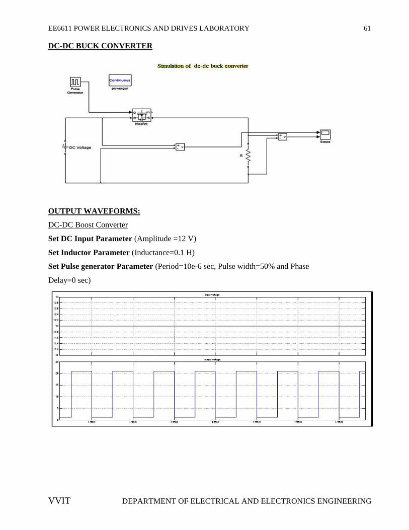
EE6611 POWER ELECTRONICS AND DRIVES LABORATORY 61
VVIT DEPARTMENT OF ELECTRICAL AND ELECTRONICS ENGINEERING
DC-DC BUCK CONVERTER
OUTPUT WAVEFORMS:
DC-DC Boost Converter
Set DC Input Parameter (Amplitude =12 V)
Set Inductor Parameter (Inductance=0.1 H)
Set Pulse generator Parameter (Period=10e-6 sec, Pulse width=50% and Phase
Delay=0 sec)
EE6611 POWER ELECTRONICS AND DRIVES LABORATORY 62
VVIT DEPARTMENT OF ELECTRICAL AND ELECTRONICS ENGINEERING
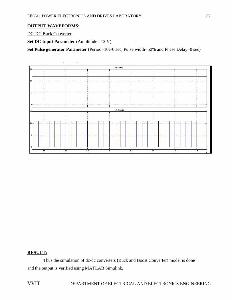
OUTPUT WAVEFORMS:
DC-DC Buck Converter
Set DC Input Parameter (Amplitude =12 V)
Set Pulse generator Parameter (Period=10e-6 sec, Pulse width=50% and Phase Delay=0 sec)
RESULT:
Thus the simulation of dc-dc converters (Buck and Boost Converter) model is done
and the output is verified using MATLAB Simulink.
EE6611 POWER ELECTRONICS AND DRIVES LABORATORY 62
VVIT DEPARTMENT OF ELECTRICAL AND ELECTRONICS ENGINEERING
OUTPUT WAVEFORMS:
DC-DC Buck Converter
Set DC Input Parameter (Amplitude =12 V)
Set Pulse generator Parameter (Period=10e-6 sec, Pulse width=50% and Phase Delay=0 sec)
RESULT:
Thus the simulation of dc-dc converters (Buck and Boost Converter) model is done
and the output is verified using MATLAB Simulink.

EE6611 POWER ELECTRONICS AND DRIVES LABORATORY 63
VVIT DEPARTMENT OF ELECTRICAL AND ELECTRONICS ENGINEERING
Ex. No:16SIMULATION OF THREE PHASE CONVERTER
DATE:
AIM:To simulate three phase Converter circuit with RL load in MATLAB - Simulink.
APPARATUS REQUIRED:
A PC with MATLAB package.
THEORY:
Figure shows the circuit diagram of three Phase Bridge controlled rectifier. It consist of
upper group (T1,T3,T5) and lower group (T2,T4,T5) of thyristors .Thyristor T1 is forward biased ad
can be triggered for conduction only when Va is greater than both Vb and Vc. From figure this
condition occurs at wt=300. Hence T1 can be triggered only at wt=300.If firing angle is α , then T1
starts conduction at wt=30 + α and conducts for 1200 where it get commutated by turning on of next
thyristor ie,T3.Similarly triggering instant for T3 and T5 are determined when considering Vb
and Vc respectively. For lower group T4, T6 and T2, negative voltages, ie,-Va,-Vb and -Vc
respectively are considered.
AVERAGE VALUE OF OUTPUT VOLTAGE:
Where
VM – The maximum value of phase to neutral voltage
AVERAGE VALUE OF OUTPUT CURRENT:
Where
R is the load resistance
Vavg = √ VM COSα
Iavg = √ VM COSα
R
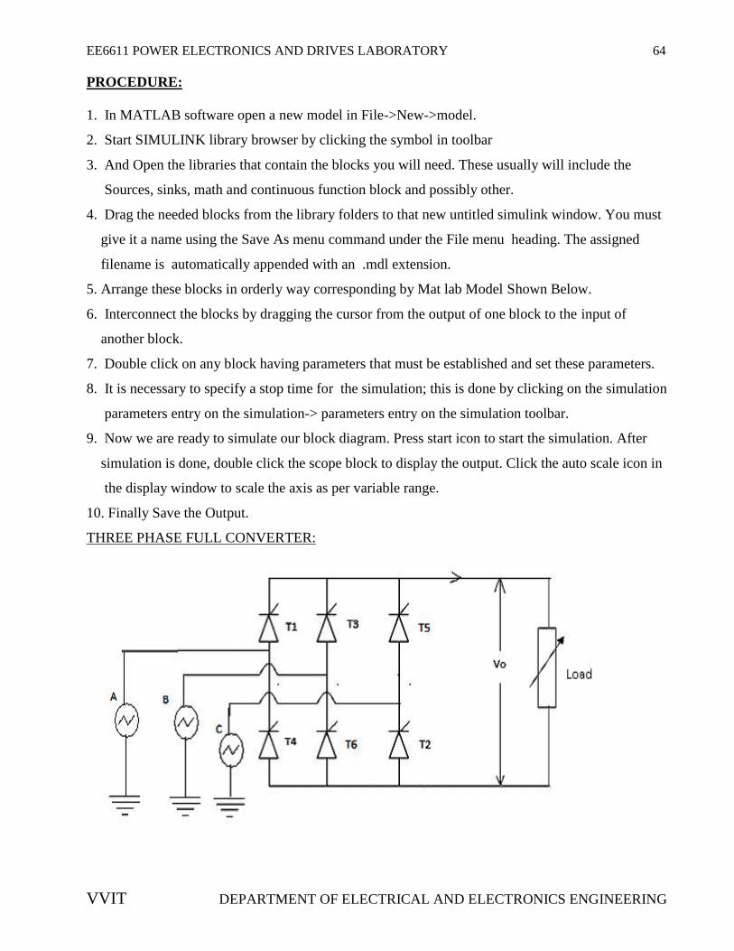
EE6611 POWER ELECTRONICS AND DRIVES LABORATORY 64
VVIT DEPARTMENT OF ELECTRICAL AND ELECTRONICS ENGINEERING
PROCEDURE:
1. In MATLAB software open a new model in File->New->model.
2. Start SIMULINK library browser by clicking the symbol in toolbar
3. And Open the libraries that contain the blocks you will need. These usually will include the
Sources, sinks, math and continuous function block and possibly other.
4. Drag the needed blocks from the library folders to that new untitled simulink window. You must
give it a name using the Save As menu command under the File menu heading. The assigned
filename is automatically appended with an .mdl extension.
5. Arrange these blocks in orderly way corresponding by Mat lab Model Shown Below.
6. Interconnect the blocks by dragging the cursor from the output of one block to the input of
another block.
7. Double click on any block having parameters that must be established and set these parameters.
8. It is necessary to specify a stop time for the simulation; this is done by clicking on the simulation
parameters entry on the simulation-> parameters entry on the simulation toolbar.
9. Now we are ready to simulate our block diagram. Press start icon to start the simulation. After
simulation is done, double click the scope block to display the output. Click the auto scale icon in
the display window to scale the axis as per variable range.
10. Finally Save the Output.
THREE PHASE FULL CONVERTER:
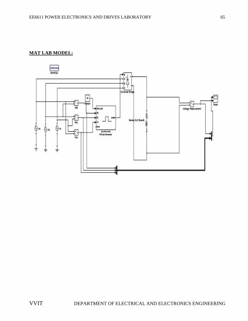
EE6611 POWER ELECTRONICS AND DRIVES LABORATORY 65
VVIT DEPARTMENT OF ELECTRICAL AND ELECTRONICS ENGINEERING
MAT LAB MODEL:
EE6611 POWER ELECTRONICS AND DRIVES LABORATORY 65
VVIT DEPARTMENT OF ELECTRICAL AND ELECTRONICS ENGINEERING
MAT LAB MODEL:
EE6611 POWER ELECTRONICS AND DRIVES LABORATORY 65
VVIT DEPARTMENT OF ELECTRICAL AND ELECTRONICS ENGINEERING
MAT LAB MODEL:

EE6611 POWER ELECTRONICS AND DRIVES LABORATORY 66
VVIT DEPARTMENT OF ELECTRICAL AND ELECTRONICS ENGINEERING
OUTPUT WAVEFORMS:
DC-DC Boost Converter
Set AC Input Parameter
(For Va : Peak amplitude =245 V, Phase=0 deg and Frequency=50 Hz)
(For Vb : Peak amplitude =245 V, Phase= -120 deg and Frequency=50 Hz)
(For Vc: Peak amplitude =245 V, Phase=120 deg and Frequency=50 Hz)
Set Synchronized 6-Pulse Generator Parameter (Frequency=50 Hz, Pulse width=10 deg)
Set RL Branch Parameter (Resistance =1000 Ohms, Inductance =350e-3 H)
RESULT:
Thus the simulation of three phase converter model is done and the output is verified using
MATLAB Simulink.