l6- gate drive and snubbers
TRANSCRIPT
Power Electronic Devices and owe ec o c ev ces dCircuits (EEL-209)
By: Prof. Bhim Singh
Department of Electrical Engineering, Indian Institute of Technology Delhi,
Hauz Khas, New Delhi-10016, India- 110016email: [email protected]
Ph.:011-2659-1045 1

Gate driver circuits

Gate Driver CircuitGate Driver Circuit• Interface between control (low power electronics) and (high ( p ) ( g
power) switch.• Functions:
– Amplification: amplifies control signal to a level required to drive power switch
– Isolation: provides electrical isolation between power– Isolation: provides electrical isolation between power switch and logic level
• Complexity of driver varies markedly among switches. – MOSFET/IGBT drivers are simple– GTO and BJT drivers are very complicated and expensive.

Gate Driver Circuit
Control
Circuit
Driver
CircuitPowerswitch
The switching speeds and on-state losses of a giveng p gcontrolled switch depend on how it is controlled, so it isimportant to design the proper drive circuit
Functionality of Gate/Base Drive CircuitsFunctionality of Gate/Base Drive Circuits
T it h f ff t t t t tTurn power switch from off-state to on-state
Minimize turn-on time through active region where
power dissipation is large
Provide adequate drive power to keep power switch
in on-state

Functionality of Gate/Base Drive CircuitsFunctionality of Gate/Base Drive Circuits
T it h f t t t ff t tTurn power switch from on-state to off-state
• Minimize turn-off time through active region where
power dissipation is large
• Provide bias to insure that power switch remains off
Functionality of Gate/Base Drive CircuitsFunctionality of Gate/Base Drive Circuits
• Control power switch to protect it when over voltagesControl power switch to protect it when over voltages or over currents are sensed
• Signal processing circuits which generate the logic g p g g gcontrol signals not considered part of the drive circuit.
• Drive circuit amplifies control signals to levels required to drive power switch
• Drive circuit has significant power capabilities compared to logic level signal processing circuits

Drive Circuit Design ConsiderationsDrive Circuit Design Considerations
Drive circuit topologiesDrive circuit topologies• Output signal polarity - unipolar or bipolar• AC or DC coupledAC or DC coupled• Connected in shunt or series with power switch

Drive Circuit Design ConsiderationsDrive Circuit Design Considerations
Output current magnitudeOutput current magnitude• Large Ion shortens turn-on time but lengthens turn-off
delay timey• Large Ioff shortens turn-off time but lengthens turn-
on delay timeyProvisions for power switch protection
• Over currentsOve cu e s• Blanking times for bridge circuit drives

Drive Circuit Design ConsiderationsDrive Circuit Design Considerations
Wave shaping to improve switch performanceWave shaping to improve switch performance
• Controlled d /d for BJT turn-offControlled diB/dt for BJT turn-off• Anti-saturation diodes for BJT drives• Speedup capacitors• Speedup capacitors• Front-porch/back porch currents
Component layout to minimize stray inductance and shielding from switching noiseshielding from switching noise
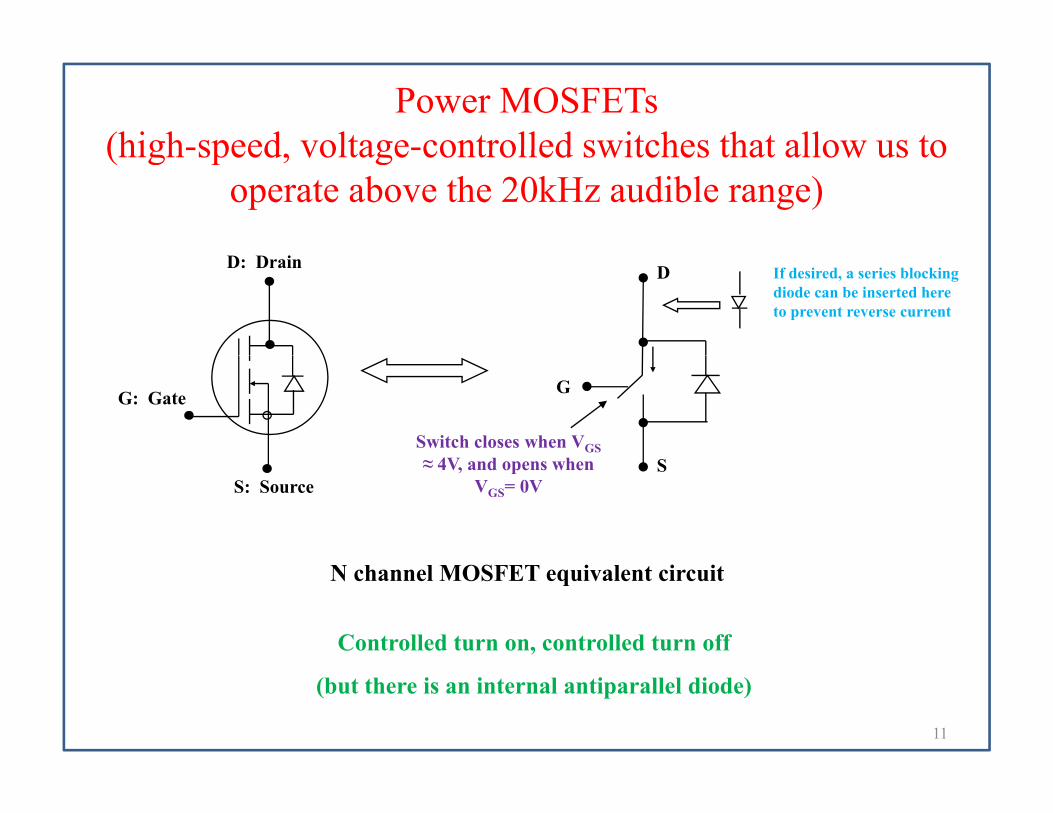
Power MOSFETs(high-speed voltage-controlled switches that allow us to(high speed, voltage controlled switches that allow us to
operate above the 20kHz audible range)
D: Drain If desired, a series blocking diode can be inserted here to prevent reverse current
D
G: Gate
Switch closes when VGS4V d h
G
S: Source≈ 4V, and opens when
VGS= 0VS
N channel MOSFET equivalent circuit
Controlled turn on, controlled turn off
11
(but there is an internal antiparallel diode)

We Avoid the Linear (Lossy) Region, Using Only the We vo d t e ea ( ossy) eg o , Us g O y t eOn and Off States
MOSFET “off”MOSFET “on”
DD
SS
when VGS = 12V when VGS = 0V
12

We Want to Switch Quickly to Minimize Switching LossesTurn Off Turn On
VDS(t)
Turn Off
VDS(t)
Turn On
I( ) I( )Δt ff Δt0 0
I(t) I(t)Δtoff Δton
PLOSS(t) PLOSS(t)
0 0
Energy lost per turn off
Energy lost per turn on00
13
Turn off and turn on times limit the frequency of operation because their sum must be considerably less than period T (i.e., 1/f)

Consider, for example, the turn off
VDS(t)
Turn Off
VEnergy lost per turn off is proportional to
0
V • I • Δtoff ,
so we want to keep turn off (and turn on) times as small as possible
I(t)
I
times as small as possible.
The more often we switch, the more “energy
P (t) Δtoff
0loss areas” we experience per second.
Thus, switching losses (average W) are PLOSS(t) Δtoff
0Energy lost per turn off
, g ( g )proportional to switching frequency f, V, I, Δtoff, and Δton.
14
And, of course, there are conduction losses that are proportional to squared I
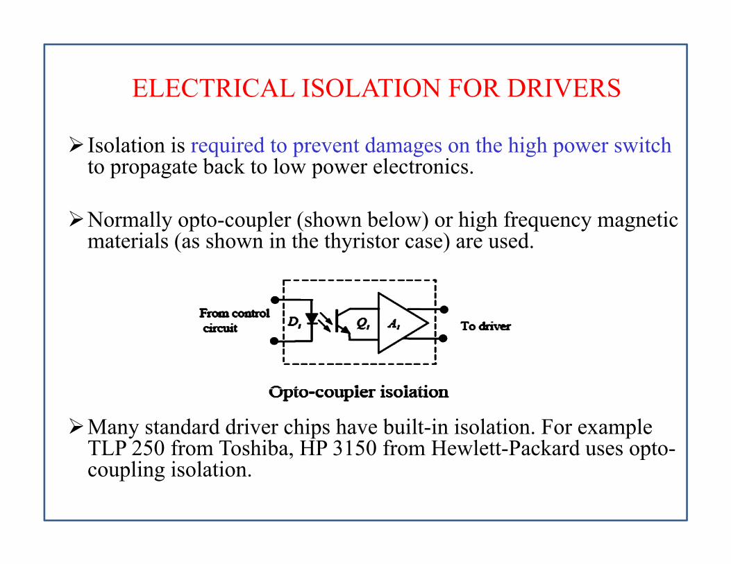
ELECTRICAL ISOLATION FOR DRIVERS
Isolation is required to prevent damages on the high power switchto propagate back to low power electronics.p p g p
Normally opto-coupler (shown below) or high frequency magnetic materials (as shown in the thyristor case) are used.materials (as shown in the thyristor case) are used.
Many standard driver chips have built-in isolation. For example TLP 250 from Toshiba, HP 3150 from Hewlett-Packard uses opto-coupling isolation.
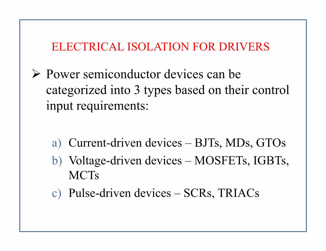
ELECTRICAL ISOLATION FOR DRIVERSELECTRICAL ISOLATION FOR DRIVERS
Power semiconductor devices can bePower semiconductor devices can be categorized into 3 types based on their control input requirements:put equ e e ts:
a) Current driven devices BJTs MDs GTOsa) Current-driven devices – BJTs, MDs, GTOsb) Voltage-driven devices – MOSFETs, IGBTs,
MCTMCTsc) Pulse-driven devices – SCRs, TRIACs

CURRENT DRIVEN DEVICES (BJT)
Power BJT devices have low current gain due to constructionalPower BJT devices have low current gain due to constructionalconsideration, leading current than would normally be expectedfor a given load or collector current.
h i bl i h hi i i i h l ff iThe main problem with this circuit is the slow turn-off time.

ELECTRICALLY ISOLATED DRIVE CIRCUITS
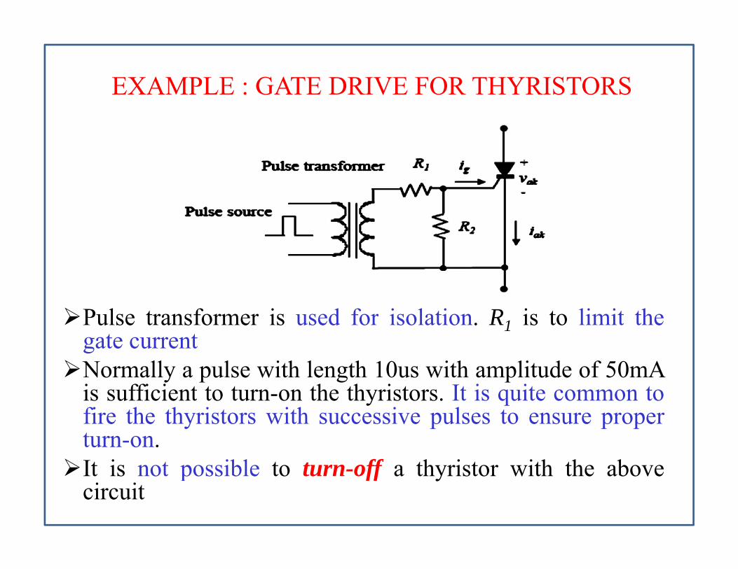
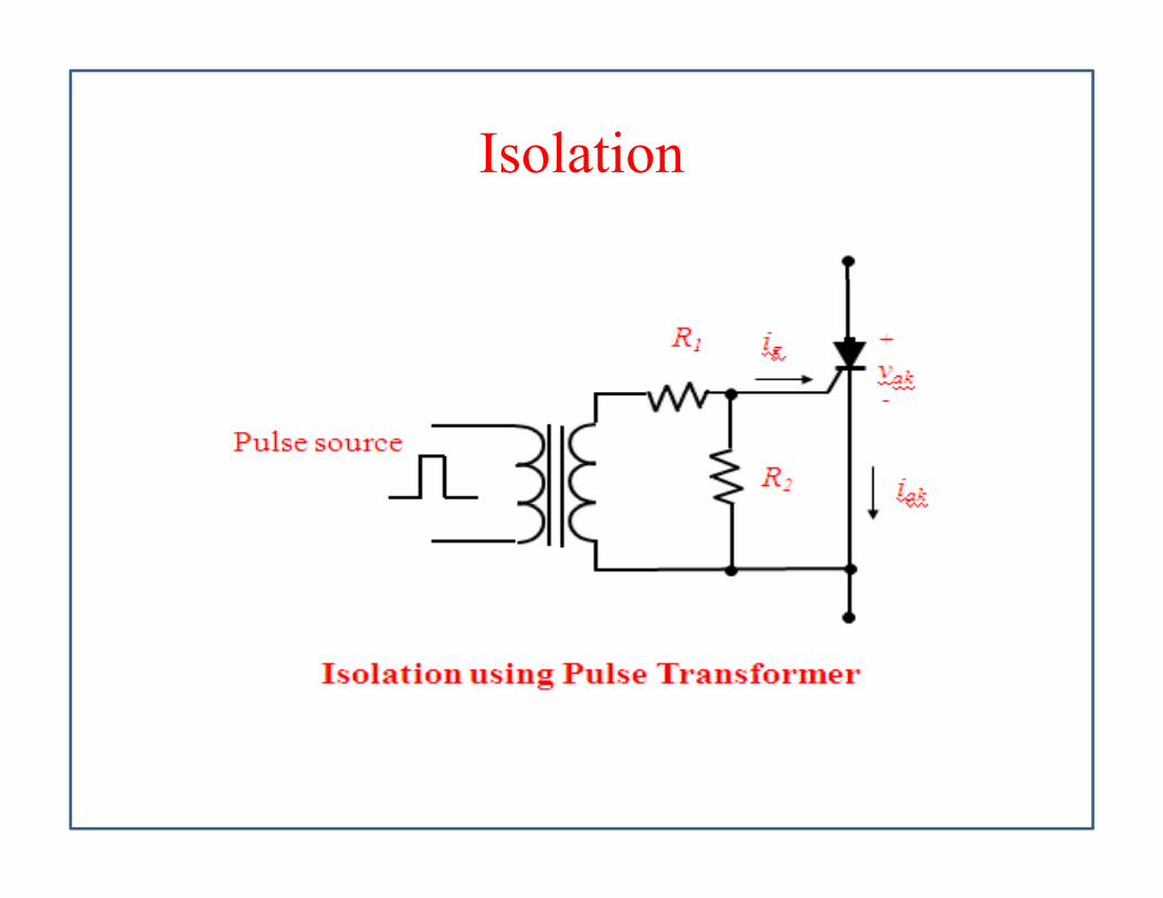
EXAMPLE : GATE DRIVE FOR THYRISTORS
Pulse transformer is used for isolation R1 is to limit thePulse transformer is used for isolation. R1 is to limit thegate currentNormally a pulse with length 10us with amplitude of 50mAis sufficient to turn on the thyristors It is quite common tois sufficient to turn-on the thyristors. It is quite common tofire the thyristors with successive pulses to ensure properturn-on.It i t ibl t t ff th i t ith th bIt is not possible to turn-off a thyristor with the abovecircuit
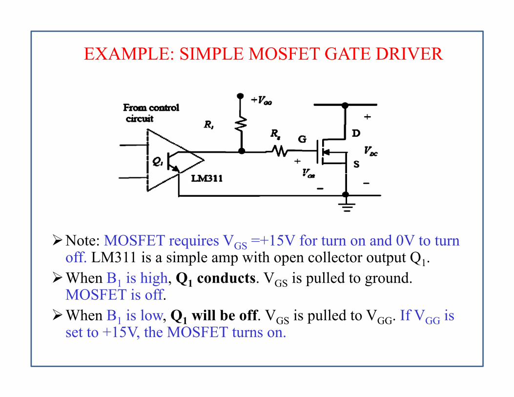
EXAMPLE: SIMPLE MOSFET GATE DRIVER
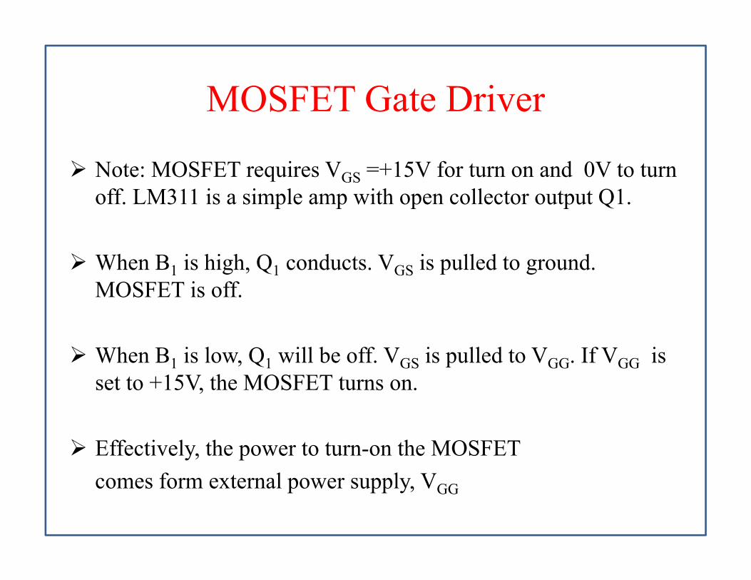
Note: MOSFET requires VGS =+15V for turn on and 0V to turn off. LM311 is a simple amp with open collector output Q1.Wh B i hi h Q d t V i ll d t dWhen B1 is high, Q1 conducts. VGS is pulled to ground. MOSFET is off.When B1 is low, Q1 will be off. VGS is pulled to VGG. If VGG is 1 1 GS GG GGset to +15V, the MOSFET turns on.
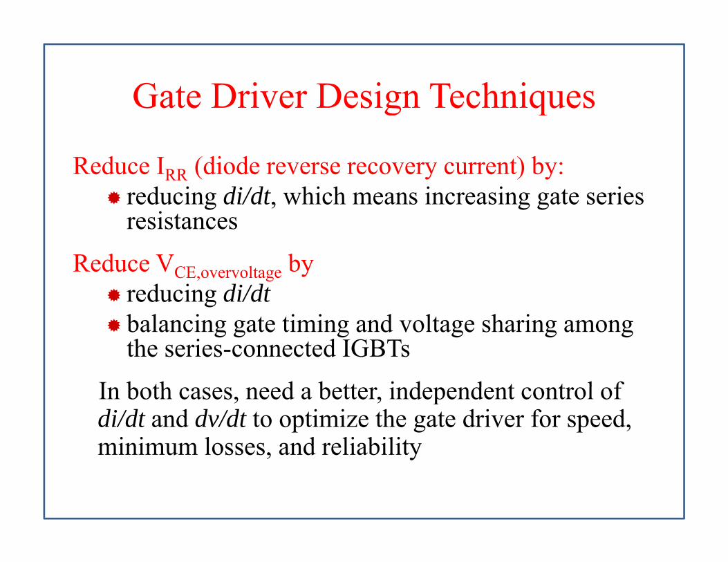
Gate Driver Design TechniquesGate Driver Design Techniques
Reduce IRR (diode reverse recovery current) by:RR ( y ) yreducing di/dt, which means increasing gate series resistances
Reduce VCE,overvoltage byreducing di/dtb l i t ti i d lt h ibalancing gate timing and voltage sharing among the series-connected IGBTs
In both cases need a better independent control ofIn both cases, need a better, independent control of di/dt and dv/dt to optimize the gate driver for speed, minimum losses, and reliability, y
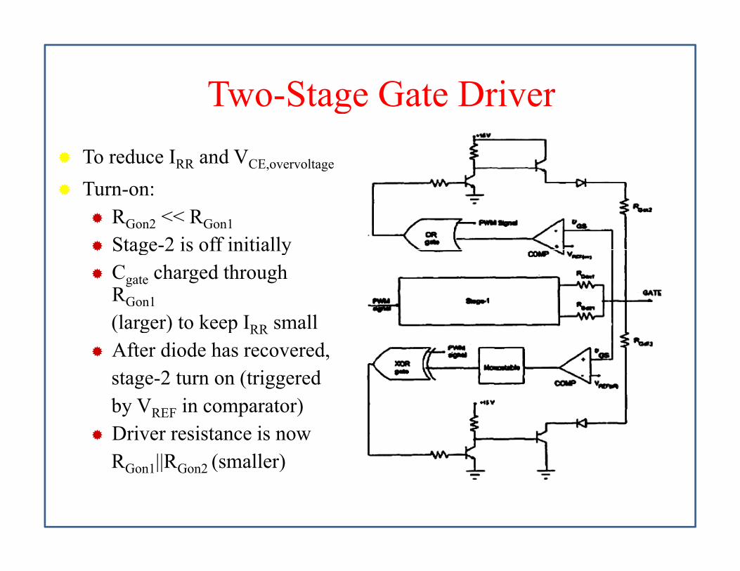
Two-Stage Gate DriverTwo Stage Gate DriverTo reduce IRR and VCE,overvoltage
Turn-on:RGon2 << RGon1
Stage-2 is off initiallyStage 2 is off initiallyCgate charged through RGon1
(larger) to keep I small(larger) to keep IRR smallAfter diode has recovered,stage-2 turn on (triggeredby VREF in comparator)Driver resistance is nowRG 1||RG 2 (smaller)RGon1||RGon2 (smaller)
Two-Stage Gate Driverg
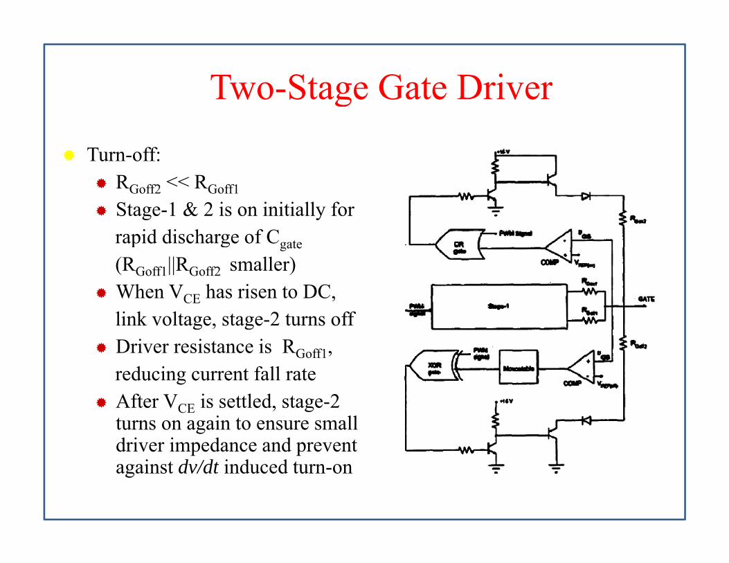
Turn-off:R RRGoff2 << RGoff1
Stage-1 & 2 is on initially forrapid discharge of Cgatep g gate
(RGoff1||RGoff2 smaller)When VCE has risen to DC,link voltage stage 2 turns offlink voltage, stage-2 turns offDriver resistance is RGoff1,reducing current fall rateAfter VCE is settled, stage-2 turns on again to ensure small driver impedance and prevent against dv/dt induced turn-on
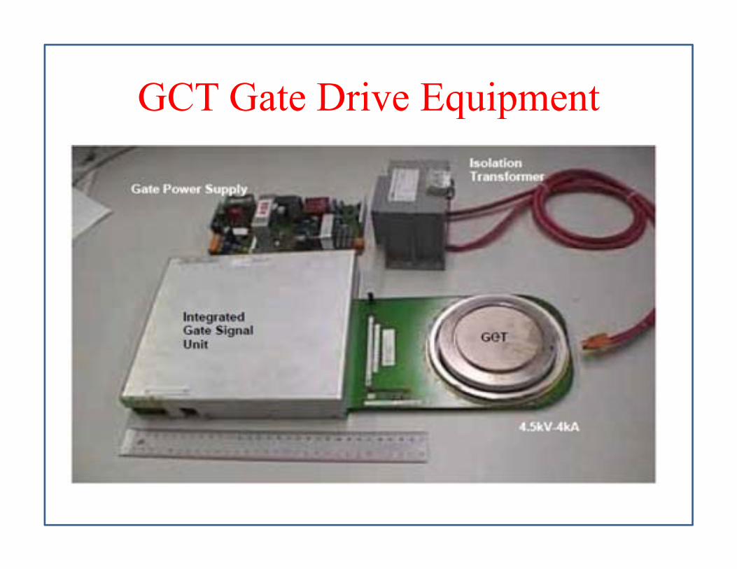
GCT Gate Drive EquipmentGCT Gate Drive Equipment
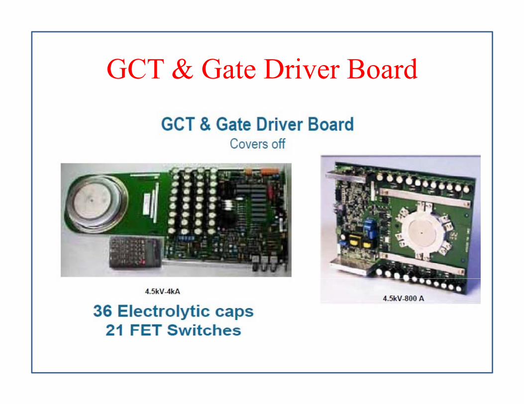
GCT & Gate Driver BoardGCT & Gate Driver Board
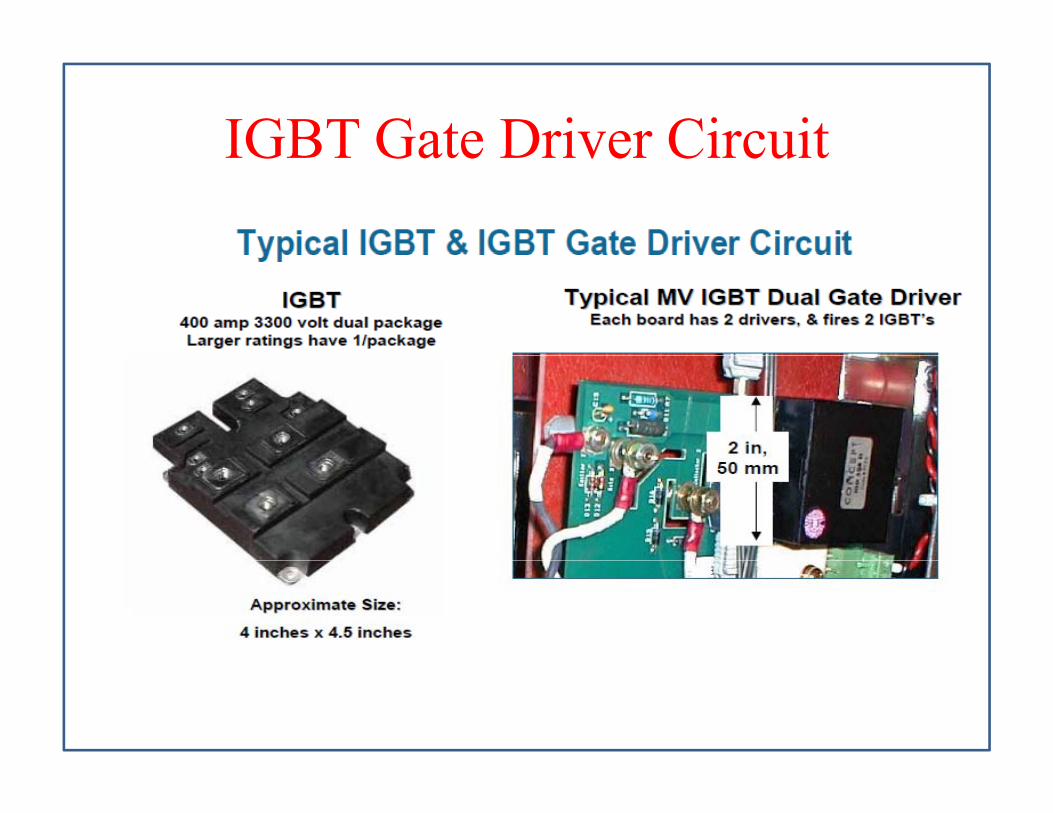
IGBT Gate Driver CircuitIGBT Gate Driver Circuit

IGET Gate Driver EquipmentIGET Gate Driver EquipmentInjection enhanced insulated gate bipolar transistor

Calculated Reliability of Gate DriversCalculated Reliability of Gate Drivers

Power Devices LossesPower Devices Losses
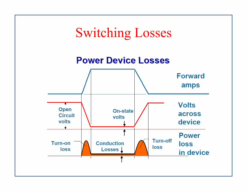
Switching LossesSwitching Losses

Power Devices Switching LossesPower Devices Switching Losses

Power Devices Switching LossesPower Devices Switching Losses

Power Switch Voltage and Current RatingsPower Switch Voltage and Current Ratings

Power Switch Voltage and Current RatingsPower Switch Voltage and Current Ratings
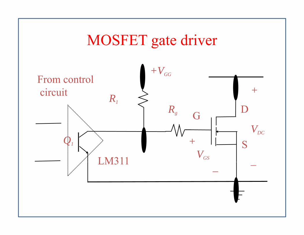
MOSFET gate driverMOSFET gate driver
+VGG
+From controlcircuit
+VGG
R1
VDC
DG1
Rg
VDC
S+VGSLM311
Q1
__LM311
MOSFET Gate DriverMOSFET Gate Driver
Note: MOSFET requires VGS =+15V for turn on and 0V to turn q GSoff. LM311 is a simple amp with open collector output Q1.
When B1 is high, Q1 conducts. VGS is pulled to ground. MOSFET is off.
When B1 is low, Q1 will be off. VGS is pulled to VGG. If VGG is set to +15V, the MOSFET turns on.
Effectively, the power to turn-on the MOSFET f l lcomes form external power supply, VGG
IsolationIsolation
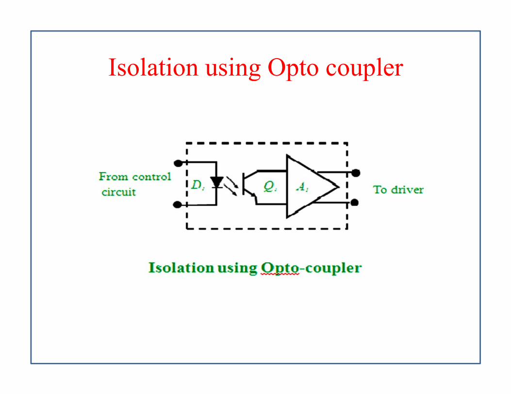
Isolation using Opto couplerIsolation using Opto coupler

Need for Isolation for Gate Driver CircuitNeed for Isolation for Gate Driver Circuit

Opto-Coupler Isolated BJT DrivesOpto Coupler Isolated BJT Drives
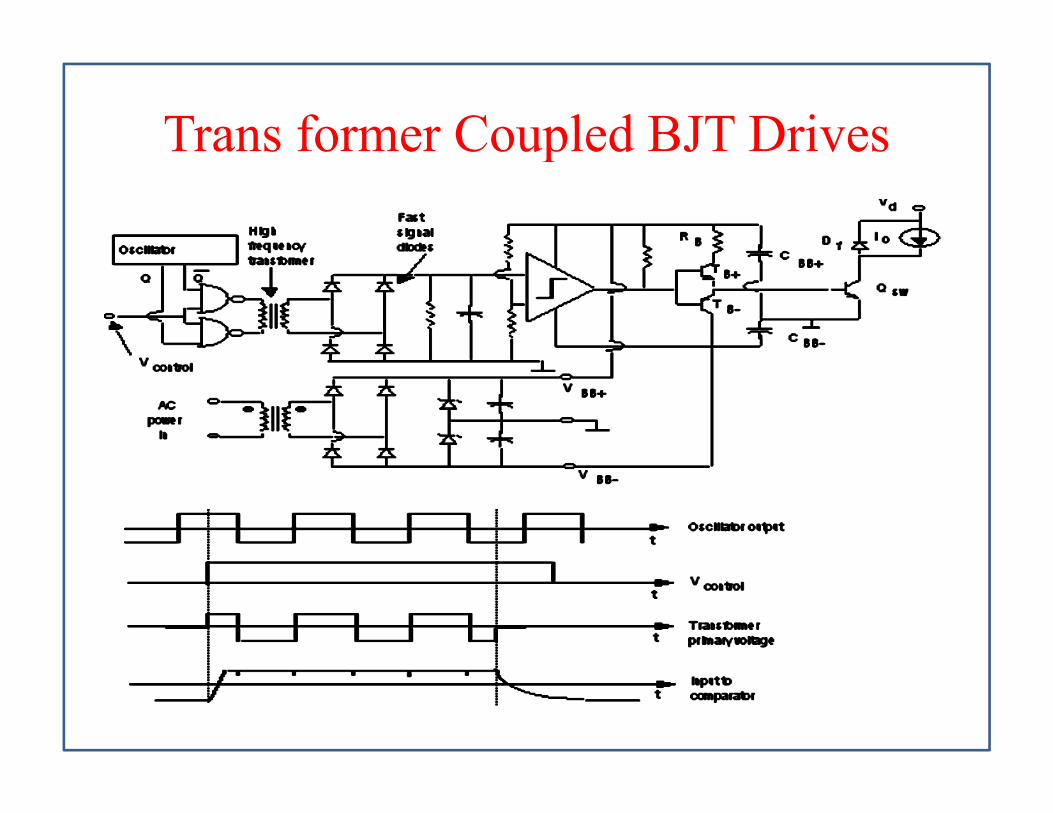
Trans former Coupled BJT DrivesTrans former Coupled BJT Drives
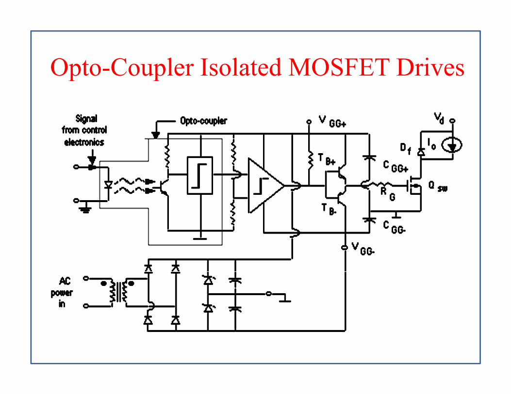
Opto-Coupler Isolated MOSFET DrivesOpto Coupler Isolated MOSFET Drives

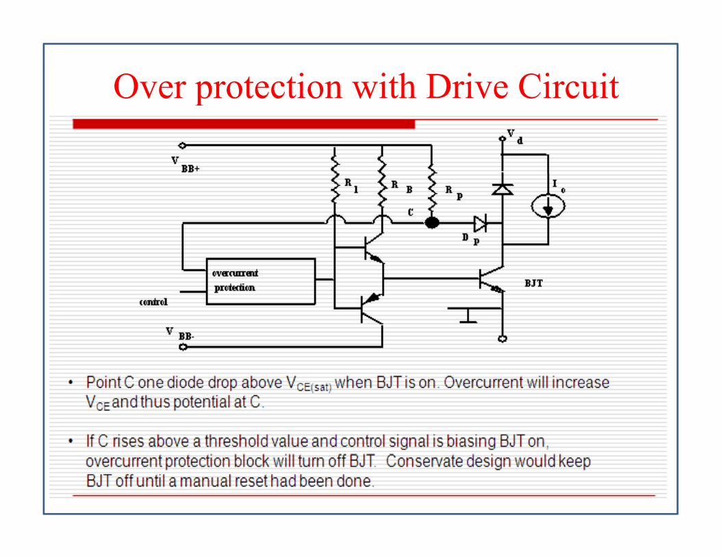
Over protection with Drive Circuitp
Snubber Circuits and Heat Sinks
45

Need for protection in power semiconductor devices?For reliable operation of a device specified ratings should not be exceededFor reliable operation of a device specified ratings should not be exceeded.
But In practice, device may be subjected to over voltages or over currents.
During turn-on, di/dt may be prohibitively large.
There may be false triggering by high value of dv/dt.
A spurious signal across gate-cathode terminals may lead to unwanted turn-on.
Th d i t b t t d i t ll h b l diti fThe device must be protected against all such abnormal conditions forsatisfactory and reliable operation of SCR circuit and the equipment.
The object of this section is to discuss various techniques adopted for theThe object of this section is to discuss various techniques adopted for theprotection of SCRs.

Power semiconductor devices are commonly protectedPower semiconductor devices are commonly protected
against:1. Over-current;
2. di/dt;
3. Voltage spike or over-voltage;
4. dv/dt ;
5. Gate-under voltage;
6 Over voltage at gate;6. Over voltage at gate;
7. Excessive temperature rise;
8 El t t ti di h8. Electro-static discharge;
di/dt protection:pIf the rate of rise of anode current, i.e. di/dt, is large as compared to the
spread velocity of carriers, local hot spots will be formed near the gateconnection on account of high current density.
This localised heating may destroy the thyristor. Therefore, the rate of risef d h i f b k b l h ifi dof anode current at the time of turn-on must be kept below the specified
limiting value.
The value of di/dt can be maintained below acceptable limit by using aThe value of di/dt can be maintained below acceptable limit by using asmall inductor, called di/dt inductor, in series with the anode circuit. Typicaldi/dt limit values of SCRs are 20-500 A/µ sec.
Local spot heating can also be avoided by ensuring that the conductionspreads to the whole area as rapidly as possible. This can be achieved byapplying a gate current nearer to (but never greater than) the maximumpp y g g ( g )specified gate current.

dv/dt protection:pIf the rate of rise of forward voltage dVa/dt is high, the charging current i
will be more.
This charging current plays the role of gate current and turns on the SCReven when gate signal is zero. Such phenomena of turning-on a thyristor,
ll d d /d b id d i l d f l i f hcalled dv/dt turn-on must be avoided as it leads to false operation of thethyristor circuit.
For controllable operation of the thyristor the rate of rise of forward anodeFor controllable operation of the thyristor, the rate of rise of forward anodeto cathode voltage dVa/dt must be kept below the specified rated limit.Typical values of dv/dt are 20 – 500 V/µsec.
False turn-on of a thyristor by large dv/dt can be prevented by using asnubber circuit in parallel with the device

Overview of Snubber Circuits for Hard-S it h d C tSwitched Converters
Function to Protect the Semiconductor devices byy
• Limiting device voltages during turn-off transients
• Limiting device currents during turn- on transients• Limiting device currents during turn- on transients
• Limiting the rate-of-rise (di/dt) of currents through the
i d d i d isemiconductor device at device turn-on
• Limiting the rate-of-rise (dv/dt) of voltages across the
semiconductor device at device turn-off or during forward
blocking voltages
50
• Shaping the switching trajectory of the device as it turns on/off

Hard switching•Hard switching refers to thestressful switching behavior of thepower electronic devicespower electronic devices.•During the turn-on and turn-offtime, the power device has towithstand high voltage and currentsimultaneously, resulting in highswitching losses and stresses.g
Dissipative passive snubbers areusually added to the power circuitsso that the dv/dt and di/dt of theso that the dv/dt and di/dt of thepower devices could be reduced,So the switching loss and stress are
di d h i bb
51
diverted to the passive snubbercircuits.

Classification of snubbers
There are mainly 2 types of classification of snubbers1 Active snubbers1. Active snubbers2. Passive snubbers• Active snubbers can importantly reduce switching losses, these include
transistors and other active switches that often imply extra circuitry.Disadvantages of active snubbers
• But they need extra circuitry to control the active switch making more• But they need extra circuitry to control the active switch making morecomplex circuits which are not appropriate to all applications and theincrease in complexity of controlling these elements.
P i bbPassive snubbers• Passive snubbers are relatively simple to design and they can reduce
switching losses. Passive snubbers are limited to resistors, capacitors,inductors and diodes.
52
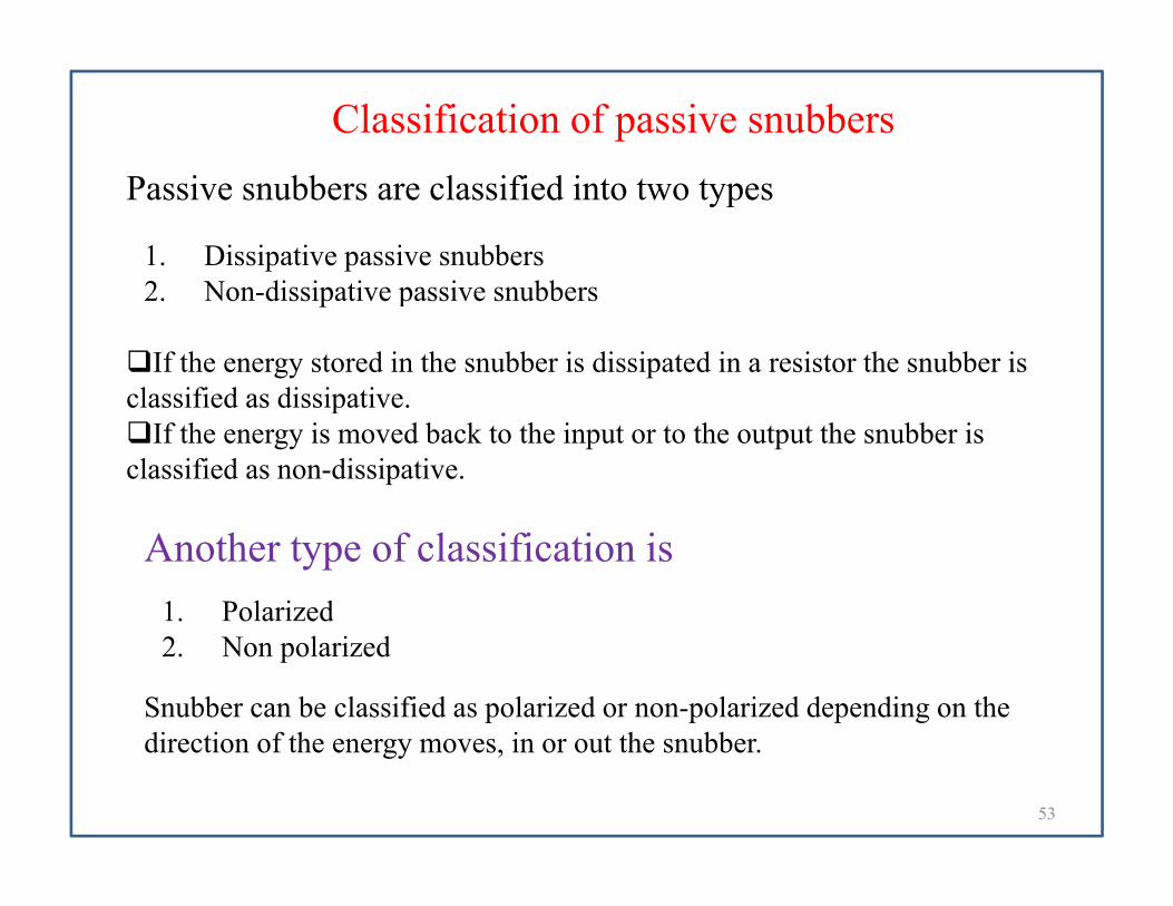
Classification of passive snubbersPassive snubbers are classified into two types
1. Dissipative passive snubbers2 N di i i i bb2. Non-dissipative passive snubbers
If the energy stored in the snubber is dissipated in a resistor the snubber is classified as dissipativeclassified as dissipative.
If the energy is moved back to the input or to the output the snubber is classified as non-dissipative.
Another type of classification is 1. Polarized2. Non polarized
Snubber can be classified as polarized or non-polarized depending on the direction of the energ mo es in or o t the sn bber
53
direction of the energy moves, in or out the snubber.
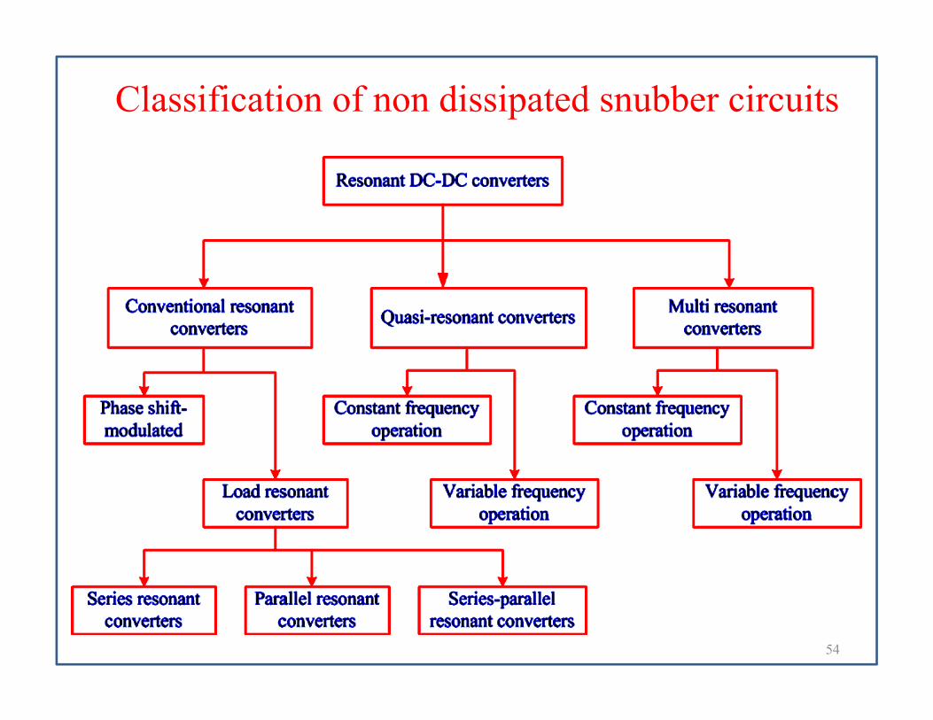
Classification of non dissipated snubber circuits
54
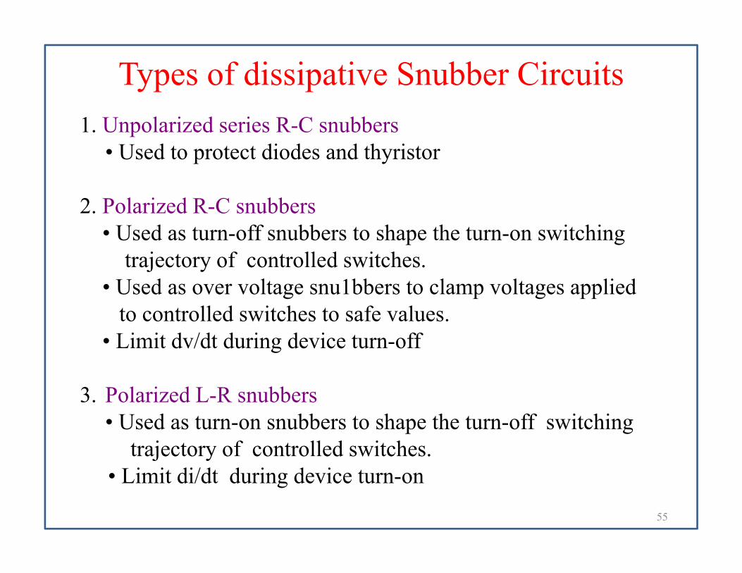
Types of dissipative Snubber Circuits1. Unpolarized series R-C snubbers
• Used to protect diodes and thyristor
2. Polarized R-C snubbers• Used as turn-off snubbers to shape the turn-on switching
trajectory of controlled switches.• Used as over voltage snu1bbers to clamp voltages applied
to controlled switches to safe values. • Limit dv/dt during device turn-off
3 Polarized L R snubbers3. Polarized L-R snubbers• Used as turn-on snubbers to shape the turn-off switching
trajectory of controlled switches. • Limit di/dt during device turn-on
55
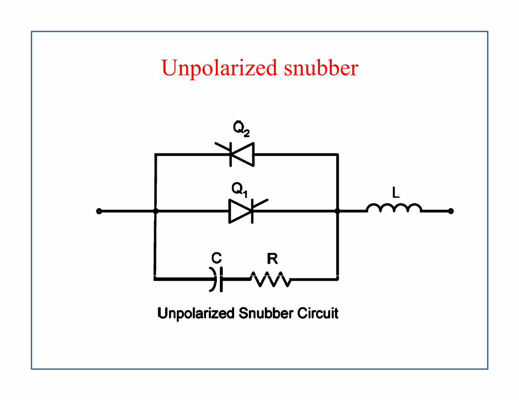
Unpolarized snubberUnpolarized snubber

Forward Polarized snubberForward Polarized snubber
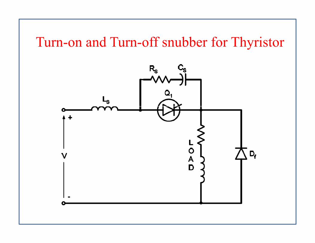
Turn-on and Turn-off snubber for ThyristorTurn on and Turn off snubber for Thyristor
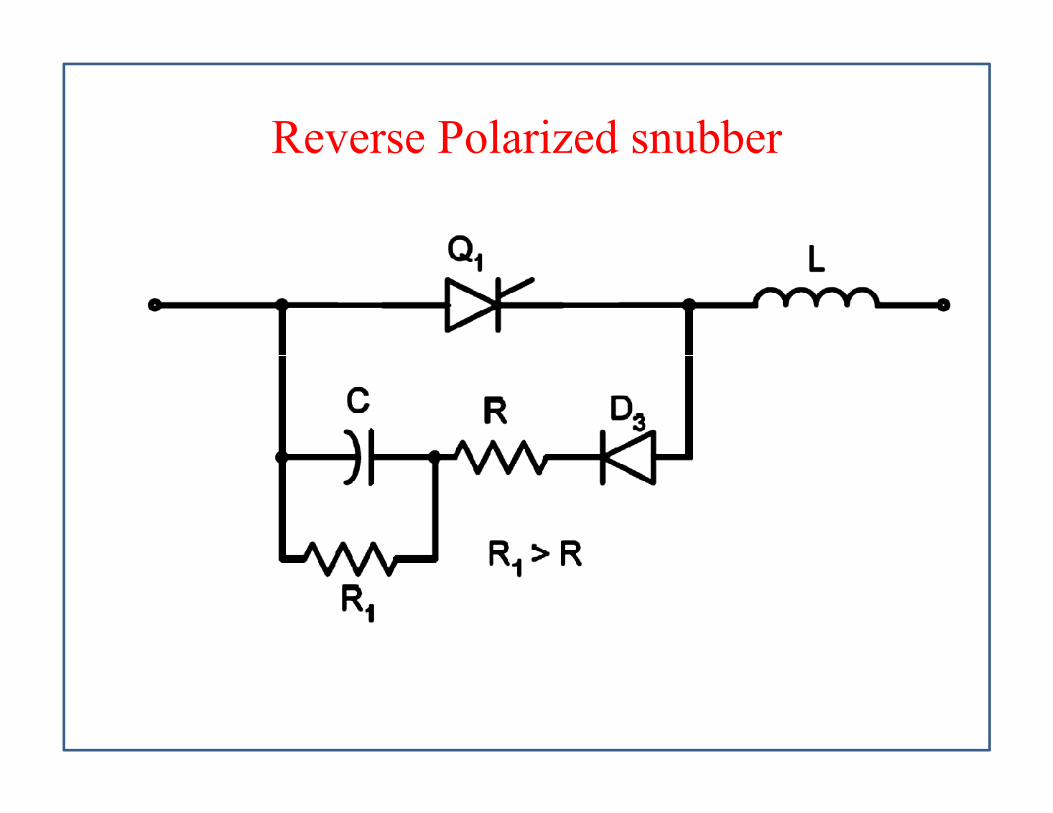
Reverse Polarized snubberReverse Polarized snubber
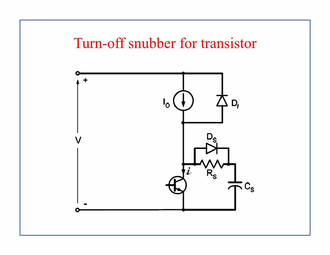
Turn-off snubber for transistorTurn off snubber for transistor
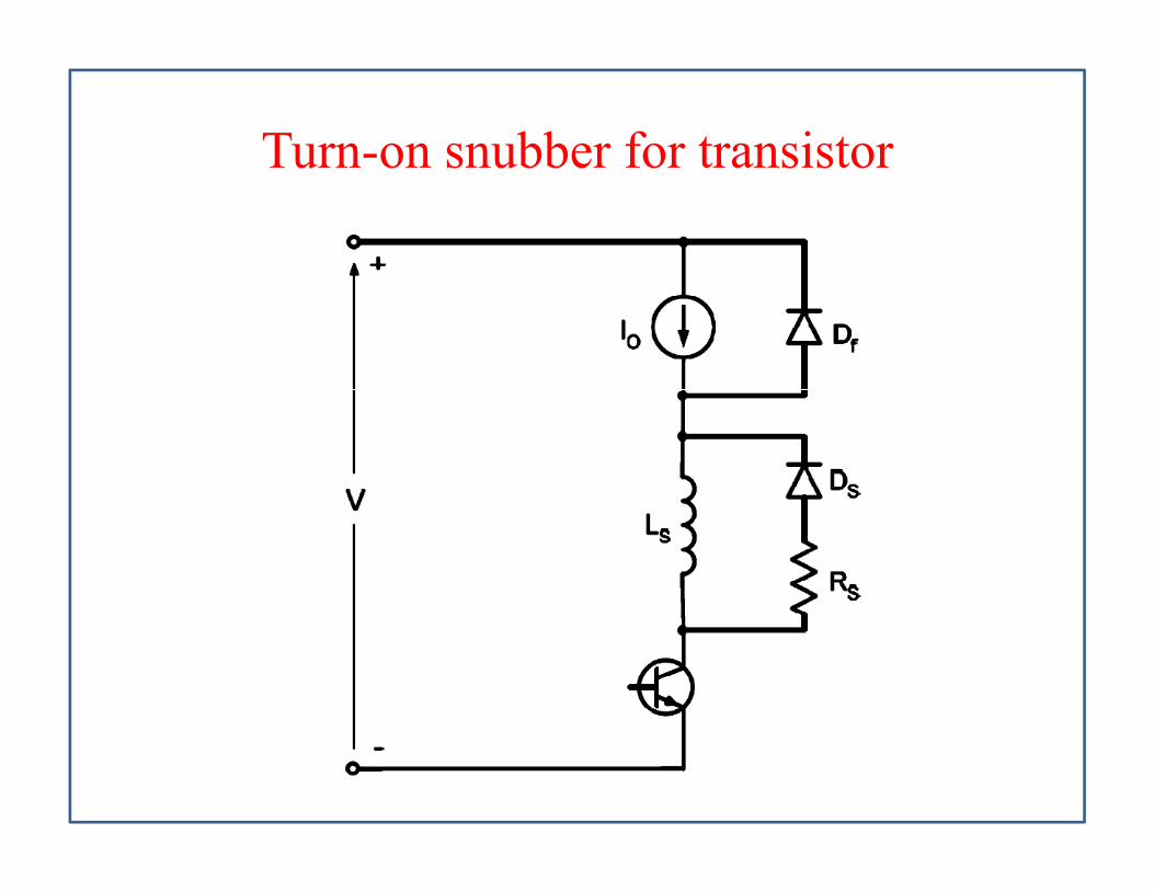
Turn-on snubber for transistorTurn on snubber for transistor

Over voltage snubber for transistorOver voltage snubber for transistor
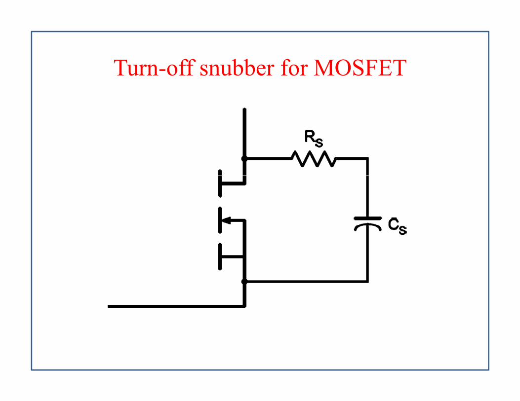
Turn-off snubber for MOSFETTurn off snubber for MOSFET
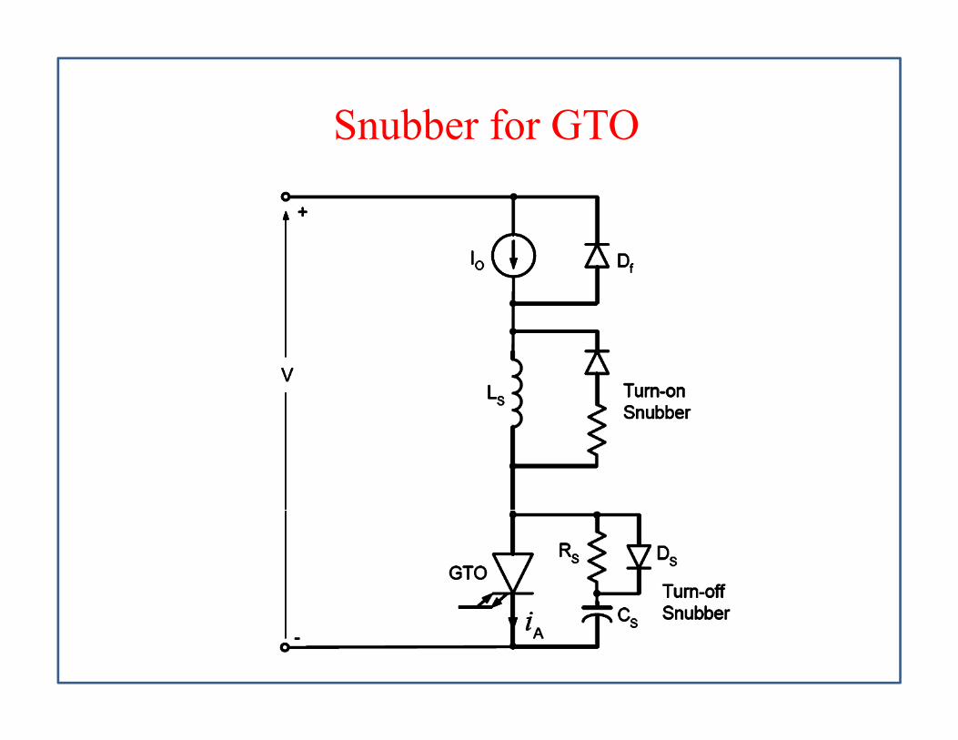
Snubber for GTOSnubber for GTO
ReferencesReferences1. N. Mohan, T. M. Undeland and W. P. Robbins, “Power
Electronics, Converter, Application and Design”, Second , , pp g ,Edition, John Willey & Sons, 1995, New York, ISBN 9971-51-177-0.
2. M. H. Rashid, “Power Electronics, circuits, Devices andApplications”, Second Edition, Prentice-Hall, 1995, India,ISBN 81-203-0869-7.
3. B. W. Williams, “Power Electronics: Devices, Drivers andli i il kApplications”,Wiley,1987.NewYork,ISBN: 0470206969.
4. W. C. Lander, "Power Electronics", 3rd Edition, McGraw-Hill, 1993, New York, ISBN: 0077077148S.
5. HOW TO SELECT A HEAT SINK. Seri Lee, Director.Advanced Thermal Engineering. Aavid ThermalTechnologies, Inc. Laconia, New Hampshire.
65

Thank youThank you
66