l12 13 system design
DESCRIPTION
MechatronicsTRANSCRIPT

Lecture 12 & 13:
Digital Implementation of Control
Circuits for Mechatronic Systems

Digital Signals
• Digital Signals have two basic states:1 (logic “high”, or H, or “on”)
0 (logic “low”, or L, or “off”)
• Digital values are in a binary format. Binary means 2 states.
• A good example of binary is a light (only onor off)

Binary
Base 2 = Base 10
000 = 0
001 = 1
010 = 2
011 = 3
100 = 4
101 = 5
110 = 6
111 = 7
In Binary, there are only 0’s and 1’s. These
numbers are called “Base-2” ( Example: 0102)
Binary to Decimal
We count in “Base-10” (0 to 9)

Binary as a Voltage
• Voltages are used to represent logic values:
• A voltage present (called Vcc or Vdd) = 1
• Zero Volts or ground (called gnd or Vss) = 0
A simple switch can provide a logic high or a logic low.

A Simple Switch
• Here is a simple switch used to provide a logic
value:
Vcc
Gnd, or 0
Vcc
Vcc, or 1
There are other ways to connect a switch.
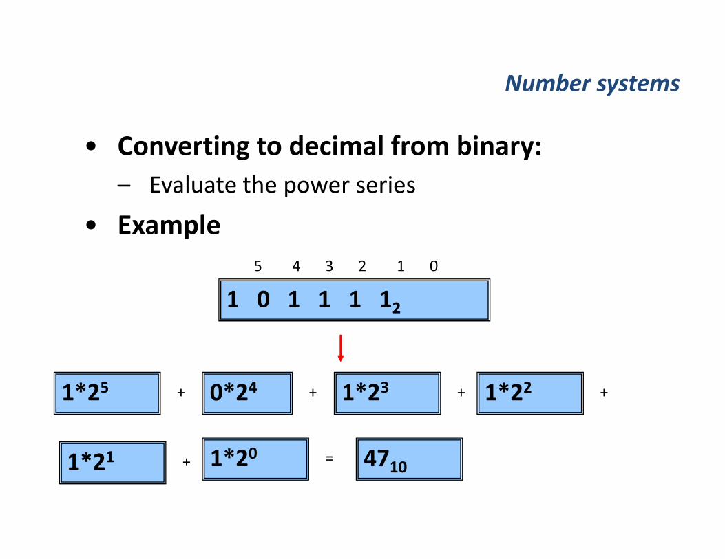
Number systems
• Converting to decimal from binary:
– Evaluate the power series
• Example
1 0 1 1 1 12
5 4 3 02 1
0*241*25 + 1*23 ++ 1*22 +
1*21 + 1*20 = 4710

Number systems
• Convert to decimal from binary:
– 1011011
a. 27
b. 91
c. 109
d. -109
e. 551

Review of Number systems
Memorize the first ten powers of two

Copyright © 2008 The McGraw-Hill Companies, Inc. Permission required for reproduction or display.
Review of Number systems

Number systems
• Converting to binary from decimal:
– Divide the decimal number by 2 repeatedly.
– The remainder gives the digits of the binary number
7462
2
2
2
2
2
2
2
2
373 R 0
186 R 1
93 R 0
46 R 1
23 R 0
11 R 1
5 R 1
2
2 R 1
1 R 0
10111010102
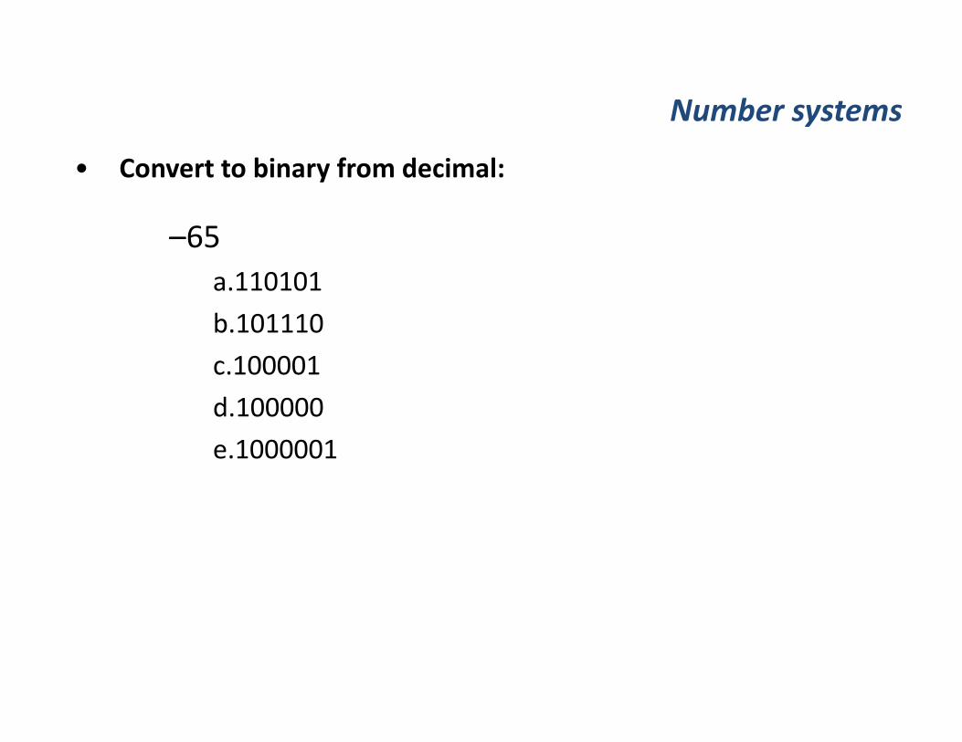
Number systems
• Convert to binary from decimal:
–65
a.110101
b.101110
c.100001
d.100000
e.1000001

Logic Gates
• Basic Digital logic is based on 3 primary
functions (the basic gates):
– AND
– OR
– NOT
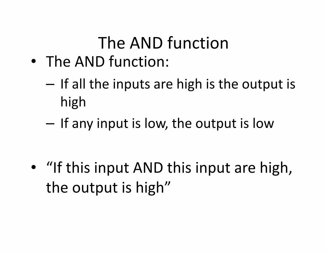
The AND function• The AND function:
– If all the inputs are high is the output is
high
– If any input is low, the output is low
• “If this input AND this input are high,
the output is high”

AND Logic Symbol
InputsOutput
If both inputs are 1, the output is 1
If any input is 0, the output is 0

AND Logic Symbol
InputsOutput
Determine the output
0
0
0

AND Logic Symbol
Inputs Output
Determine the output
0
1
0

AND Logic Symbol
InputsOutput
Determine the output
1
1
1

AND Truth Table• To help understand the function of a digital
device, a Truth Table is used:
Input Output
0 0 0
0 1 0
1 0 0
1 1 1
AND Function
Every possible input combination

AND Gates• It is possible to have AND gates with more
than 2 inputs. The same logic rules apply –
“if any input…”

The OR function• The OR function:
– if any input is high, the output is high
– if all inputs are low, the output is low
• “If this input OR this input is high,
the output is high”

OR Logic Symbol
InputsOutput
If any input is 1, the output is 1
If all inputs are 0, the output is 0

OR Logic Symbol
Inputs
Output
Determine the output
0
0
0

OR Logic Symbol
Inputs
Output
Determine the output
0
1
1

OR Logic Symbol
Inputs
Output
Determine the output
1
1
1

OR Truth Table
• Truth Table
Input Output
0 0 0
0 1 1
1 0 1
1 1 1
OR Function

The NOT function• The NOT function:
– If any input is high, the output is low
– If any input is low, the output is high
• “The output is the opposite state of the input”
• The NOT function is often called INVERTER
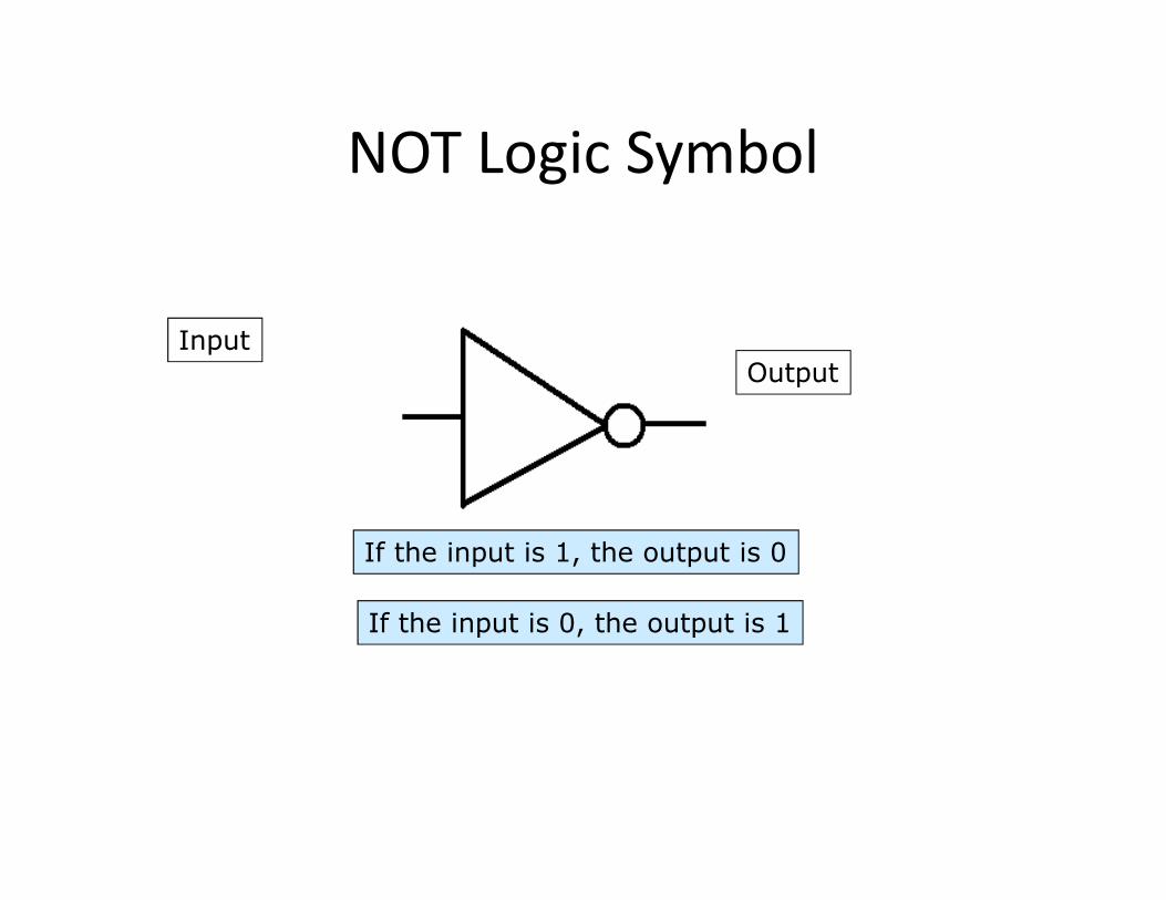
NOT Logic Symbol
Input
Output
If the input is 1, the output is 0
If the input is 0, the output is 1
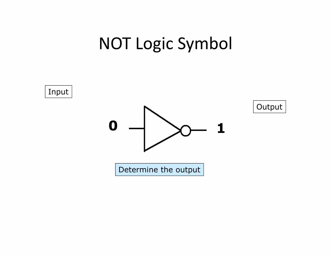
NOT Logic Symbol
Input
Output
Determine the output
0 1

NOT Logic Symbol
InputOutput
Determine the output
1 0

OR (written as +)1
a + b (read a OR b) is 1 if and only if a = 1 or b = 1 or both
AND (written as • or simply two variables catenated)
a • b = ab (read a AND b) is 1 if and only if a = 1 and b = 1.
NOT (written′)
a′ (read NOT a) is 1 if and only if a = 0
Summary

• Begins with a verbal description of the intended system, known as
the PROBLEM STATEMENT
• A block diagram of the system should be developed
• The desired objectives and constraints
Design Process for Combinational Systems

1. A system with four inputs, A, B, C, and D, and one output, Z, such
that
Z = 1 iff three of the inputs are 1.
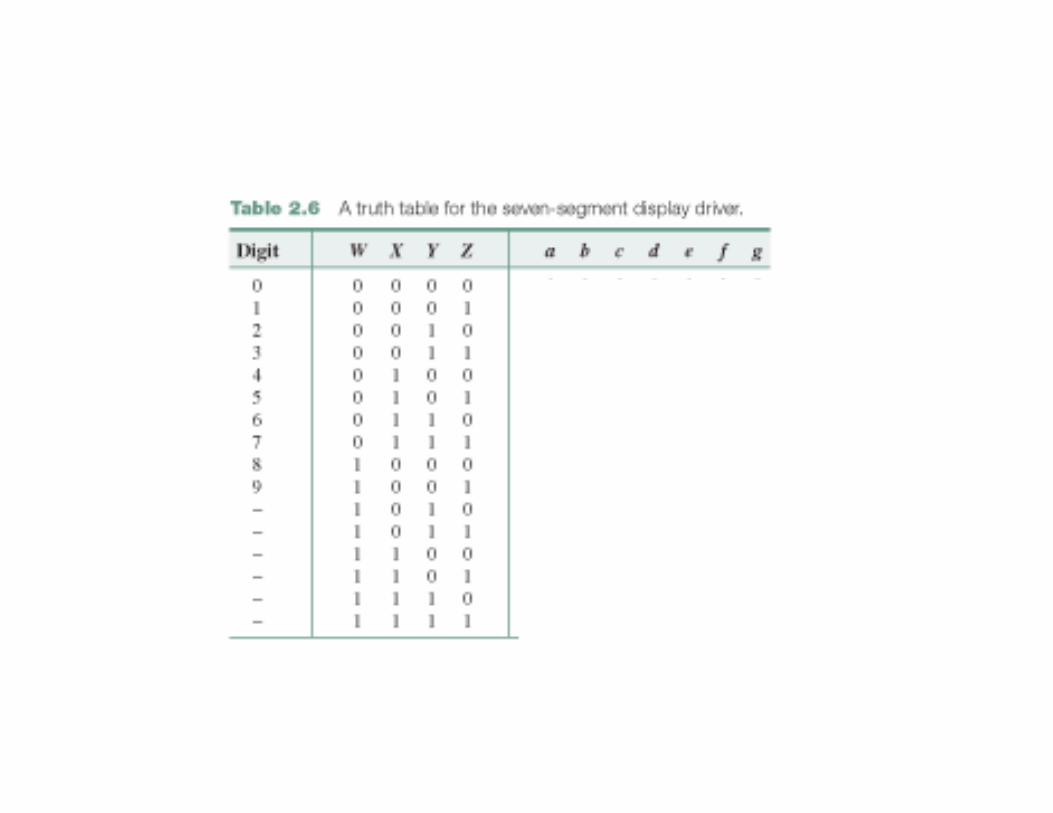
2. A system that has as its input the code for a decimal digit, and
produces as its output the signals to drive a seven-segment
display, such as those on most digital watches and numeric
displays.
Illustrations

1. Represent each of the inputs and output in binary.• This is sometimes taken care of in the problem statement (ex 1, 3, 5)
2. Formalize the design specification either in the form of a truth
table or of an algebraic expression.• There are 2n input combinations for n inputs in a truth table.
• Truth tables are written in binary order to avoid omissions.
• If necessary, break the problem into smaller sub-problems before or
after creating the truth tables.
Design Steps

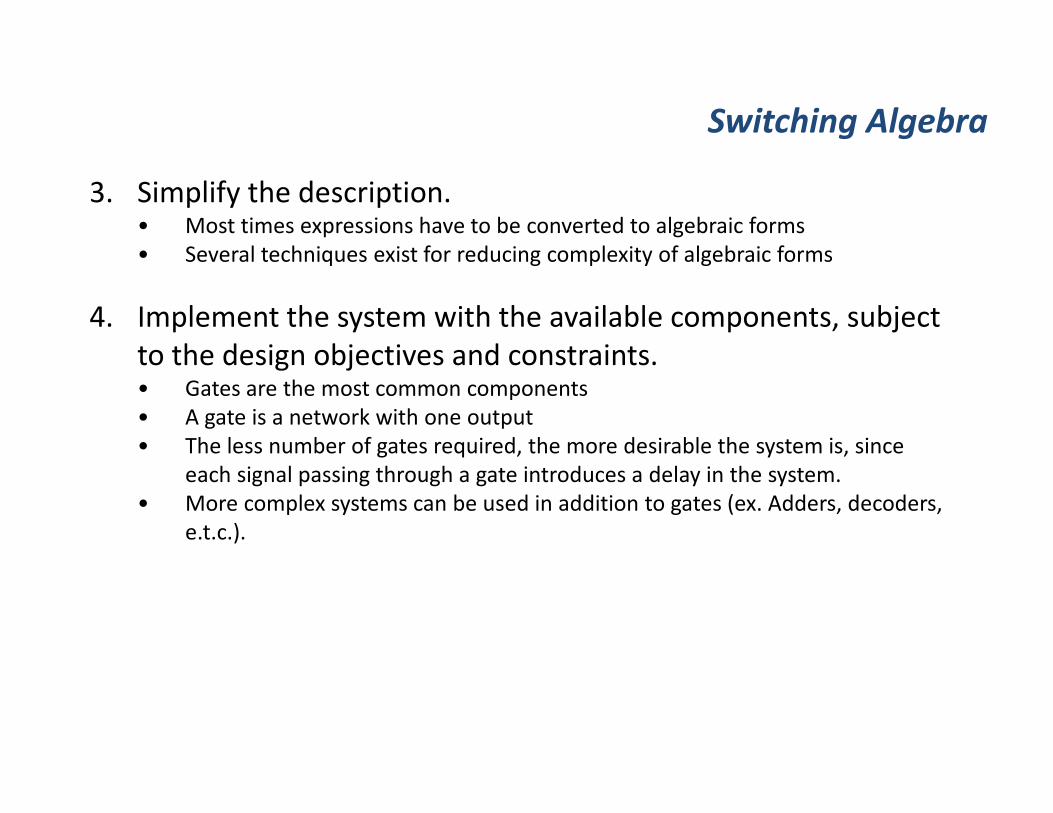
3. Simplify the description.• Most times expressions have to be converted to algebraic forms
• Several techniques exist for reducing complexity of algebraic forms
4. Implement the system with the available components, subject
to the design objectives and constraints.• Gates are the most common components
• A gate is a network with one output
• The less number of gates required, the more desirable the system is, since
each signal passing through a gate introduces a delay in the system.
• More complex systems can be used in addition to gates (ex. Adders, decoders,
e.t.c.).
Design Steps

• Don’t cares occur when
• The output is not specified for all input combinations, so
for the remaining input combinations, it doesn’t matter
• There are input combinations that don’t occur in the
system
• Flip-flops – one systems drives another
• When we just don’t care
• Don’t cares are represented by X in a truth table.
• The output of the combination could either be a 1 or a 0.
Don’t Care Conditions

Developing Truth Tables
1. A system with four inputs, A, B, C, and D, and one output, Z, such that
Z = 1 iff three of the inputs are 1.

2. A system that has as its input the code for a decimal digit, and produces as its output
the signals to drive a seven-segment display
3. Simplify the description.• Most times expressions have to be converted to algebraic forms
• Several techniques exist for reducing complexity of algebraic forms
4. Implement the system with the available components, subject
to the design objectives and constraints.• Gates are the most common components
• A gate is a network with one output
• The less number of gates required, the more desirable the system is, since
each signal passing through a gate introduces a delay in the system.
• More complex systems can be used in addition to gates (ex. Adders, decoders,
e.t.c.).
Switching Algebra


• Literal:
• The appearance of a variable or its complement.
• Product Term:
• one or more literals connected by AND operators.
• Standard product term:
• Also called minterm
• product term that includes each variable of the
problem, either uncomplemented or complemented.
• Sum of products expression (often abbreviated SOP)
• one or more product terms connected by ORoperators.
• A canonical sum or sum of standard product terms:
• a sum of products expression where all of the terms
are standard product terms.
Definitions

• A Minimum Sum of Products expression:
• one of those SOP expressions for a function that has the fewest number of product terms.
• If there is more than one expression with the fewest number of terms, then minimum is defined as one or more of those expressions with the fewest number of literals.
(1) x′yz′ + x′yz + xy′z′ + xy′z + xyz 5 terms, 15 literals
(2) x′y + xy′ + xyz 3 terms, 7 literals
(3) x′y + xy′ + xz 3 terms, 6 literals
(4) x′y + xy′ + yz 3 terms, 6 literals
Definitions

x′yz′ + x′yz + xy′z′ + xy′z + xyz 5 terms, 15 literals
= (x’yz’+x’yz)+(xy′z′ + xy′z) + xyz associative p2
= x’y(z+z’) + xy’(z+z’) + xyz distributive p8
= x’y.1 +xy’.1 +xyz complement p5
= x’y + xy’ + xyz identity p3
Simplification
Down to three terms and seven literals

x′yz′ + x′yz + xy′z′ + xy′z + xyz + xy’z 5 terms, 15 literals
= (x’yz’+x’yz)+(xy′z′ + xy′z) + (xyz + xy’z) associative p2
= x’y + xy′ + xz adjacency p9
Simplification
Down to three terms and six literals
Reduce the number of literals by adding a second copy of xy’z (or x’yz),
based on P6a – indempotency.
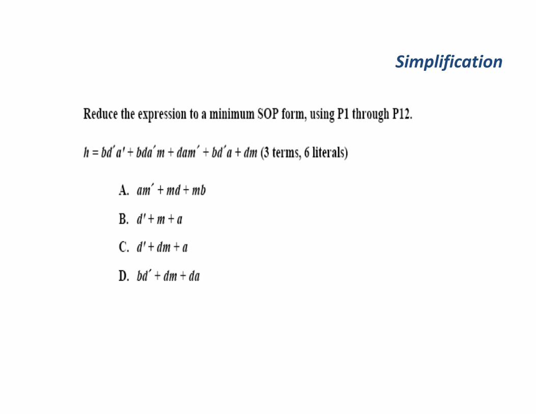
Simplification

Simplification

Sum Term: one or more literals connected by OR operators.
Standard sum term:
• also called a maxterm
• a sum term that includes each variable of the problem,
either uncomplemented or complemented.
Product of sums expression (POS):
• one or more sum terms connected by AND operators.
Canonical product or product of standard sum terms:
• a product of sums expression where all of the terms are
standard sum terms.
SOP: x′y + xy′ + xyz
POS: (x + y′)(x′ + y)(x′ + z′)
both: x′ + y + z or xyz′
neither: x(w′ + yz) or z′ + wx′y + v(xz + w′)
Definitions

Minimum sum of product
implementation of f.Circuit with only
uncomplemented inputs.
Implementation of Logic Gates
f = x’y + xy’ + xz

Implementation of Logic Gates

Implementation of Logic Gates
a. d = n’+c(h+s) (n+c’(h+s))
b. d = (n’c) + (hs) + n(hs) + c
c. d = n’c(h+s) + n(c’+(hs))
d. D = n’c(ns) + n(hs)c =

Proof of DeMorgan’s theorem.
De Morgan’s Theorem
P11a. (a+b)’ = a’b’
P11b. (ab)’ = a’+b’
Please note: (a’+b’) != a’+b’
(ab)’ != a’b’
De Morgan’s Theorem is generally used to
find the complement of an expression

De Morgan’s Theorem - Example
Find the complement of f = wx’y +xy’ +wxz
Note that f is in SOP so f’ will be in POS
• We could apply DeMorgan’s Theorem repeatdely
– f’ = (wx’y +xy’ +wxz)’
– f’ = (wx’y)’(xy’)’(wxz)’
– f’ = (w’x+y’)(x’+y)(w’+x’+z’)
• Or we could follow these set of rules
– Complement each variable
– Replace every AND by Or and every OR by AND – but make sure you keep
the order of operation

De Morgan’s Theorem - Example
Find the complement of f = ab +b’c + c’d
a. f’ = (a’ + b’+ b + c’ + c + d’)
b. f’ = (a’ + b’+ b + c’ + c + d’)’
c. f’ = a’b’+bc’+cd’
d. f’ = (a’ + b’)( b + c’) (c + d’)
e. f’ = (a’ + b’)’( b + c’)’(c + d’)’

f = a′′′′b + ab′′′′ + ab
From the truth table to Algebraic Expressions

From the truth table to Algebraic Expressions

Example
ABC f f’
000 0 1
001 1 0
010 1 0
011 1 0
100 0 1
101 0 1
110 1 0
111 1 0
f(A,B,C) = Σm(1,2,3,6,7) = ?
f’(A,B,C) = ?
a. A’B’C’ + AB’C’ + AB’C
b. B + C + D + G + H
c. A’B’C + A’BC’ + A’BC +
ABC’+ABC
d. ABC’ + AB’C + AB’C’+ A’B’C +
A’b
e. ABC + A’BC+A’BC’
a. Σm(1,2,3,6,7)’
b. Σm(0,4,5)
c. Σm(A’B’C’ + AB’C’ + AB’C)
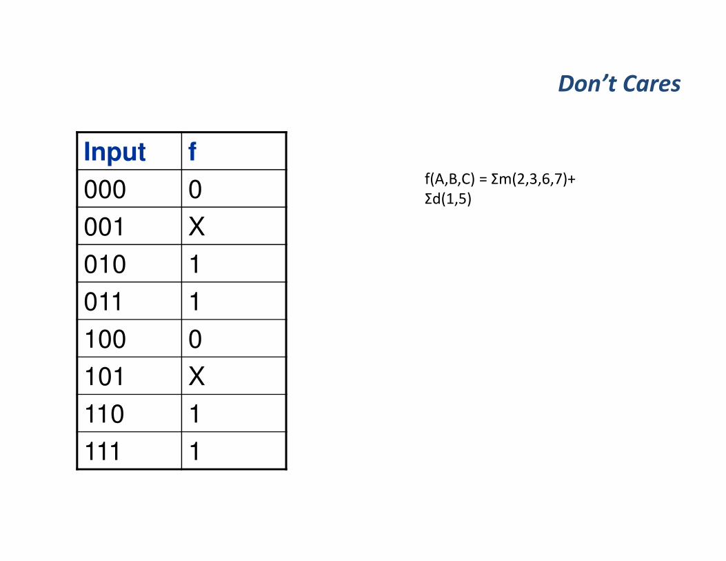
Don’t Cares
Input f
000 0
001 X
010 1
011 1
100 0
101 X
110 1
111 1
f(A,B,C) = Σm(2,3,6,7)+
Σd(1,5)

Two-variable Karnaugh maps
AB 0 1
0
1
A’B’ AB’
A’B AB
A
B
A’B’
AB 0 1
0
1
m0 m2
m1 m3

Product terms corresponding to groups of two.
Three-variable Karnaugh maps

Four-variable Karnaugh maps
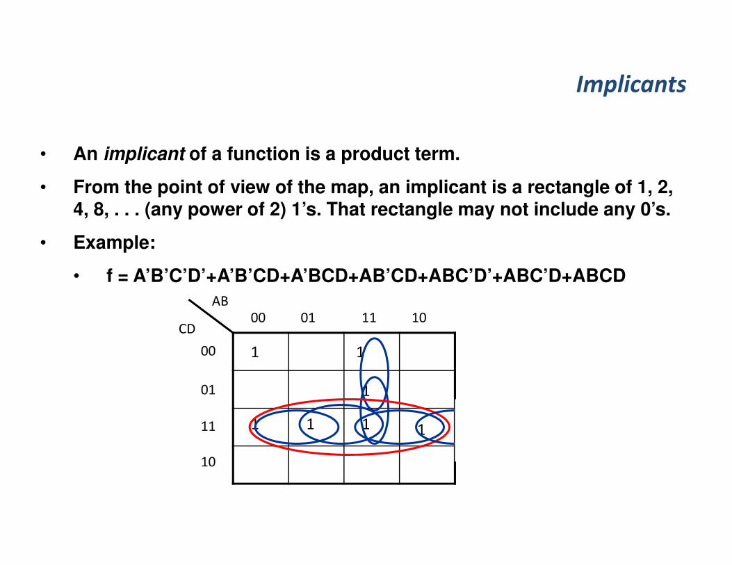
• An implicant of a function is a product term.
• From the point of view of the map, an implicant is a rectangle of 1, 2, 4, 8, . . . (any power of 2) 1’s. That rectangle may not include any 0’s.
• Example:
• f = A’B’C’D’+A’B’CD+A’BCD+AB’CD+ABC’D’+ABC’D+ABCD
Implicants
1 1
AB
CD
100
10
11
01
00 01 11 10
1
1
1
1

Implicants
• The implicants of f are:
Minterms (1 implicant)
A′′′′B′′′′C′′′′D
A′′′′B′′′′CD
A′′′′BCD
ABC′′′′D′′′′
ABC′′′′D
ABCD
AB′′′′CD
Groups of 2
A′′′′CD
BCD
ACD
B′′′′CD
ABC’
ABD
Groups of 4
CD

• Prime Implicant:
o an implicant that (from the point of view of the map) is not
fully contained in any one other implicant.
• Essential Prime Implicant:
o a prime implicant that includes at least one 1 that is not
included in any other prime implicant.
Prime and Essential Prime Implicants
1 1
100
10
11
01
00 01 11 10
1
1
1
1
AB
CD

Minimum SOP Expressions From Karnaugh Maps

1. Find all essential prime implicants.
• Circle them on the map and mark the minterm(s) that make them
essential with an asterisk (*).
2. Find enough other prime implicants to cover the function. Do this using two
criteria:
a. Choose a prime implicant that covers as many new 1’s
(that is, those not already covered by a chosen prime implicant).
b. Avoid leaving isolated uncovered 1’s.
Minimum SOP Expressions From Karnaugh Maps
The main idea is
1. To Have all ones covered
2. To Have as few terms as possible
3. To have several rectangles with more 1’s and few rectangles with less 1’s
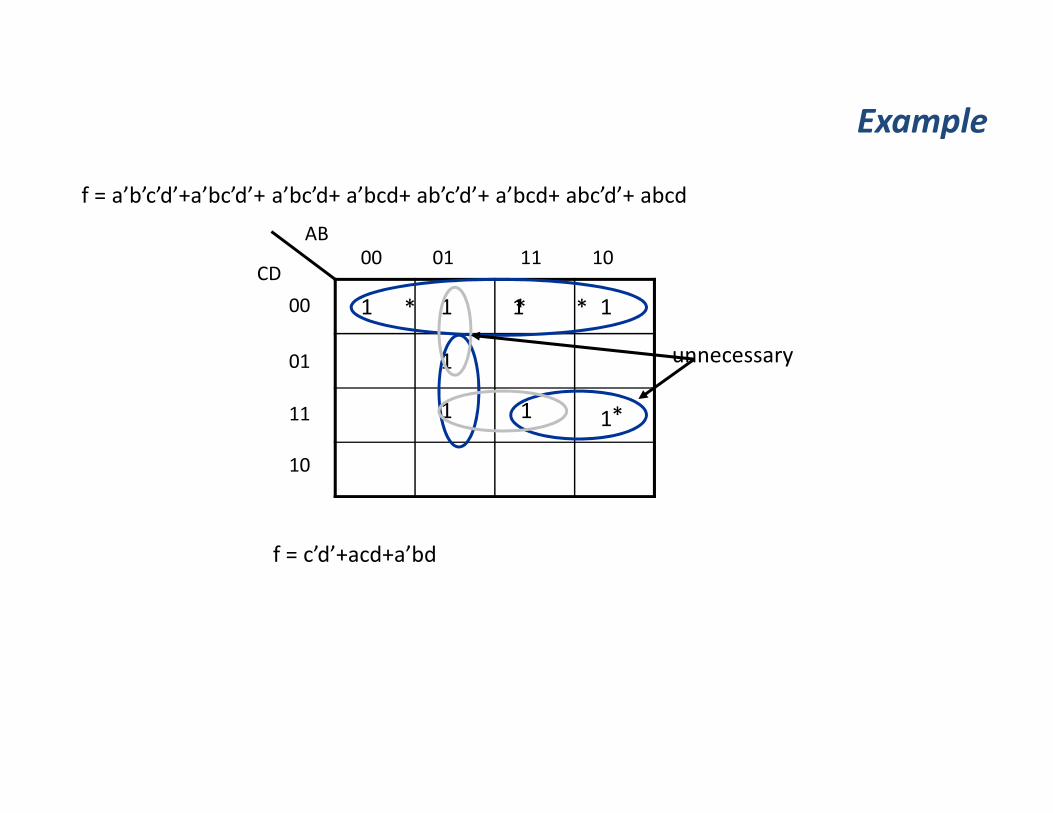
Example
f = a’b’c’d’+a’bc’d’+ a’bc’d+ a’bcd+ ab’c’d’+ a’bcd+ abc’d’+ abcd
1
1
AB
CD
100
10
11
01
00 01 11 10
1
1
1
1
1
* * *
*
f = c’d’+acd+a’bd
unnecessary

In Groups
f = b + a' c

• Prime implicant
• A rectangle of 1, 2, 4, 8, . . . 1’s or X’s not included in any
one larger rectangle.
• From the point of view of finding prime implicants, X’s
(don’t cares) are treated as 1’s.
• Essential prime implicant
• A prime implicant that covers at least one 1 not covered by
any other prime implicant (as always).
• Don’t cares (X’s) do not make a prime implicant essential.
Don’t Cares

Example
f = Σm(1,7,10,11,13) + Σd(5,8,15)
1
AB
CD
1
00
10
11
01
00 01 11 10
1
1
x
x
x
F = BD + A′C′D + AB′C
1
Use don’t cares to
get as many
minterms in each
tem as possible

• For the following problem, find the minimum SOP
expression within the options given
• h(a,b,c) = Σm(0,1,5) + d(3,4,6,7)
Example
a) h = a'b' + c + a
b) h = a + c + b’
c) h = c + b’
d) h = b’
e) h = c

Implementation of Two Functions

Example
F = A’B’C’+A’BC’+ABC’+ABC; G = A’B’C+A’BC+ABC’+ABC
F = A’C’+AB
AB
C
10
1
00 01 11 10
1 1
1
AB
C
1
0
1
00 01 11 10
1
1
1
G = A’C+AB
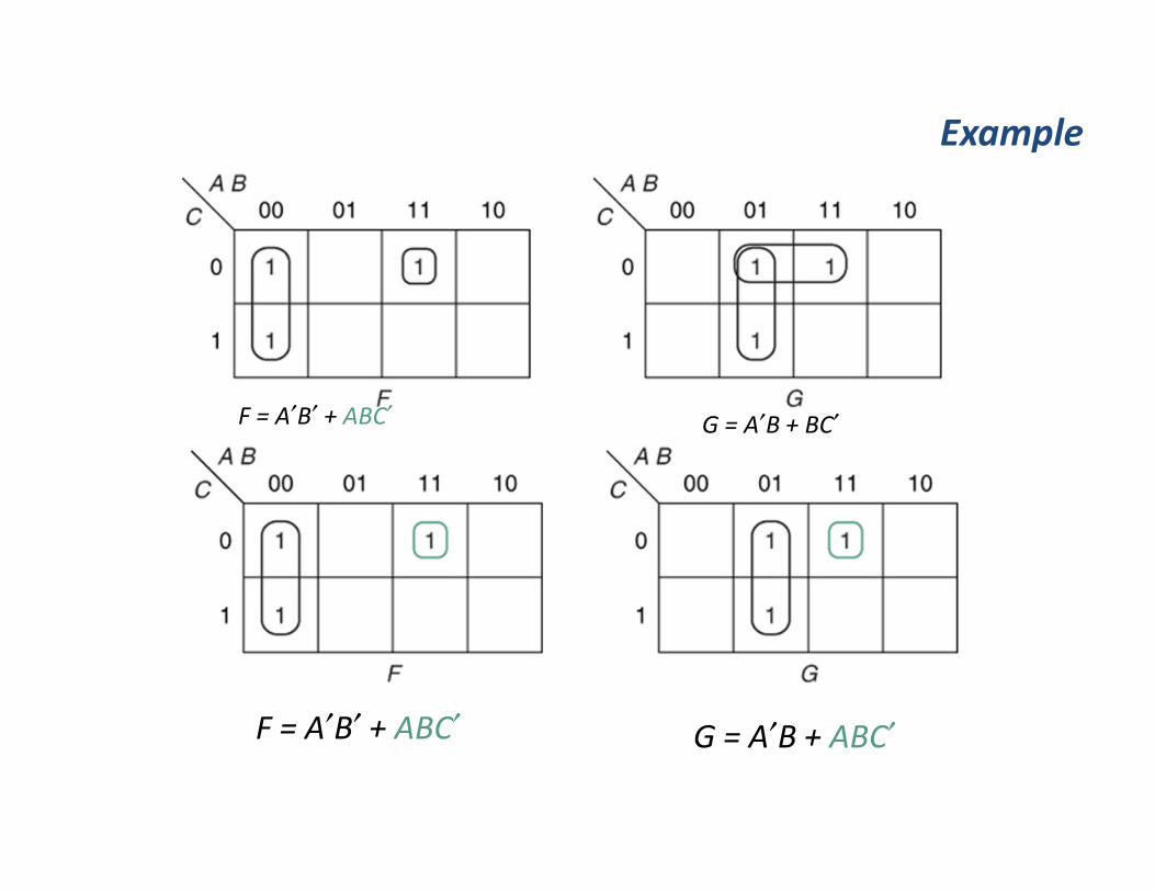
F = A′B′ + ABC′ G = A′B + BC′
F = A′B′ + ABC′ G = A′B + ABC′
Example

f = a′b + bc g = ab′ + ac
f = a′b + abc g = ab′ + abc
Example
F = A′C + A′C′D′ + AB′C G = AC′ + A′C′D′ + AB′C
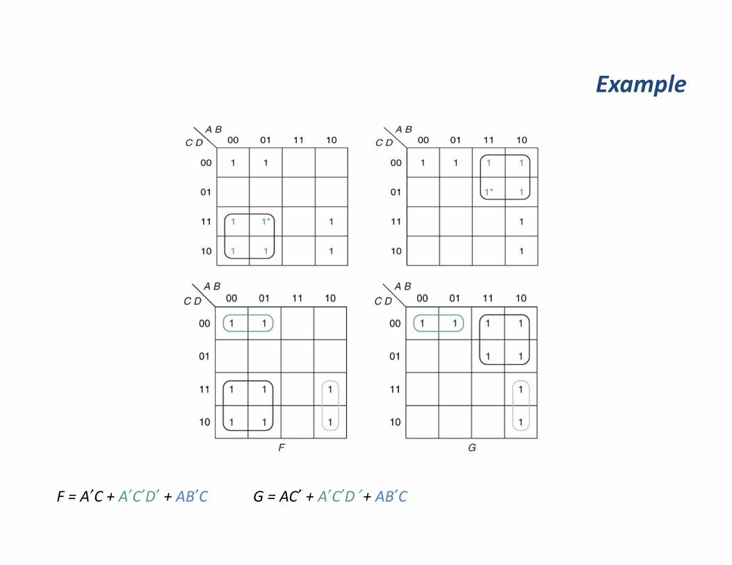
Example

Try
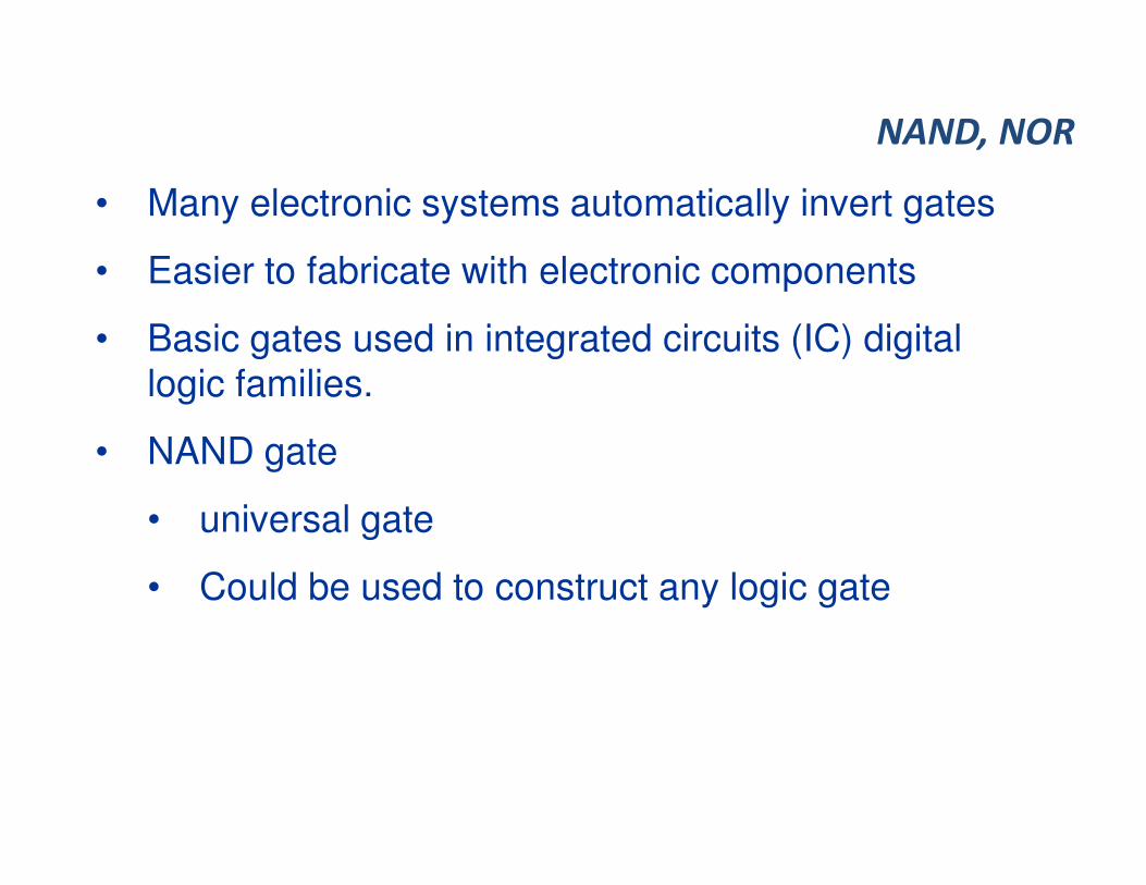
• Many electronic systems automatically invert gates
• Easier to fabricate with electronic components
• Basic gates used in integrated circuits (IC) digital logic families.
• NAND gate
• universal gate
• Could be used to construct any logic gate
NAND, NOR
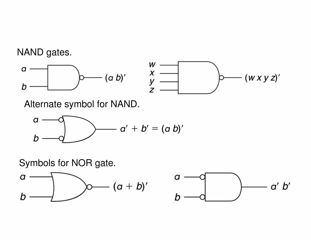
NAND gates.
Alternate symbol for NAND.
Symbols for NOR gate.
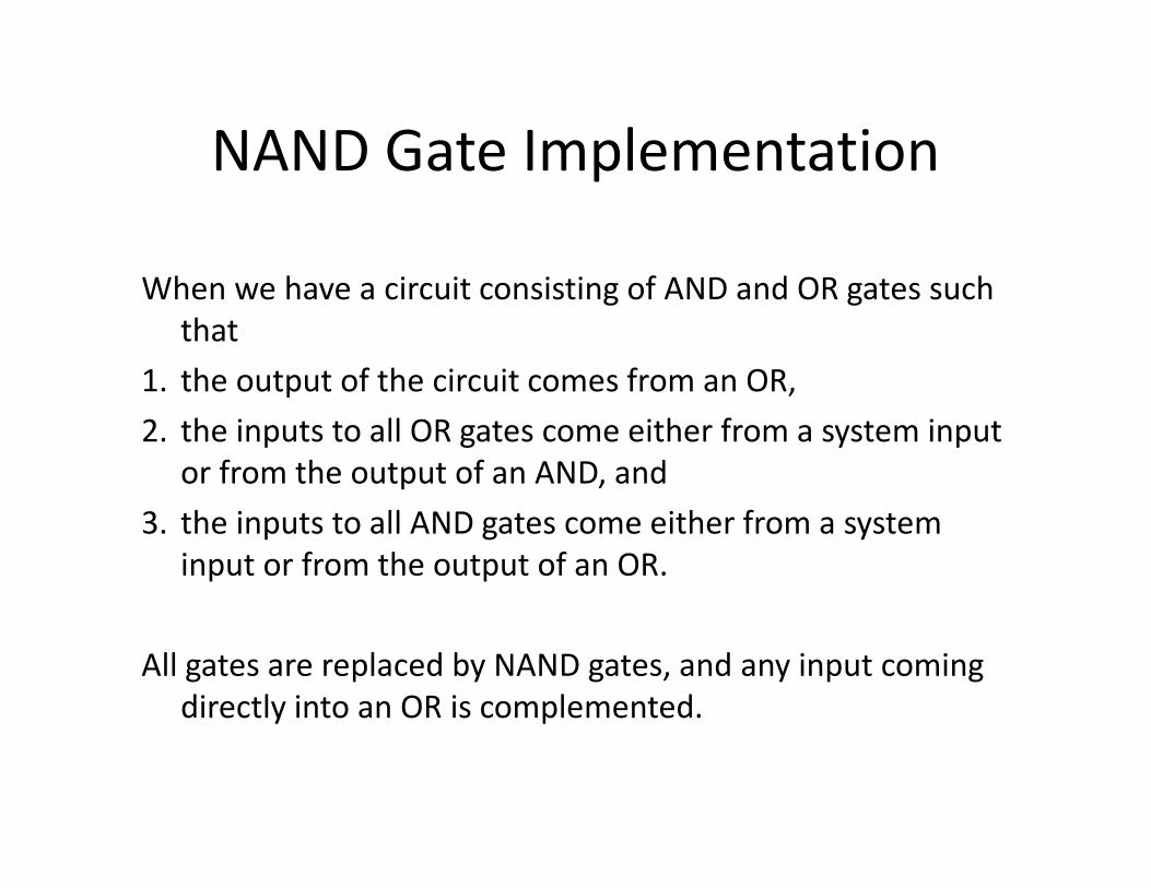
NAND Gate Implementation
When we have a circuit consisting of AND and OR gates such
that
1. the output of the circuit comes from an OR,
2. the inputs to all OR gates come either from a system input
or from the output of an AND, and
3. the inputs to all AND gates come either from a system
input or from the output of an OR.
All gates are replaced by NAND gates, and any input coming
directly into an OR is complemented.

Example
Try: g = wx(y+z)+x’y

NOR Gate Implementation
When we have a circuit consisting of AND and OR gates such
that
1. the output of the circuit comes from an AND,
2. the inputs to all OR gates come either from a system input
or from the output of an AND, and
3. the inputs to all AND gates come either from a system
input or from the output of an OR.
All gates are replaced by NOR gates, and any input coming
directly into an AND is complemented.

Example
Try: g = (x+y’)(x’+y)(x’+z)

XOR and XNOR
A xor B is 1 if a = 1 or b is 1 and 0 if both are 1 or 0;
Develop a truth table for
XOR