l -l l -c c decoder modern communication … · professor keshab k. parhi, ... digital signal...
TRANSCRIPT

LOW-LATENCY LOW-COMPLEXITY CHANNEL DECODER ARCHITECTURES FOR MODERN COMMUNICATION SYSTEMS
A DISSERTATION SUBMITTED TO THE FACULTY OF THE GRADUATE SCHOOL
OF THE UNIVERSITY OF MINNESOTA BY
Chuan Zhang
IN PARTIAL FULFILLMENT OF THE REQUIREMENTS FOR THE DEGREE OF
DOCTOR OF PHILOSOPHY
Professor Keshab K. Parhi, Advisor
December 2012

© Chuan Zhang 2012

i
Acknowledgements
First of all, I wish to thank my advisor, Professor Keshab K. Parhi, for his continuing and fatherly encouragement, guidance, and financial support throughout my entire Ph.D. study at the University of Minnesota. Before I got the admission to University of Minnesota, I was always dreaming to join this group. I am very lucky and grateful that I have had research opportunities under Professor Parhi’s supervision in the area of VLSI digital signal processing. Professor Parhi will still be my mentor even after my graduation.
I would like to thank Professor Gerald E. Sobelman, Professor Marc Riedel, and Professor Victor Reiner for their support as members of my Ph.D. committee. I would like to thank the Graduate School of University of Minnesota for their financial support by the Three-Year Graduate School Fellowship and Doctoral Dissertation Fellowship.
My thanks also go to current and former members of our research group. I would like to thank Bo Yuan for our numerous discussions on a variety of research topics. I would like to thank Yun Sang Park for his consistent engagement and help even after his graduation. I am lucky and happy to have Sohini Roy Chowdhury as one of my best friends. Also, I am grateful to Tingting Xu, Yingbo Hu, Sayed Ahmad Salehi, Te-Lung Kung, Manohar Ayinala, Yingjie Lao, Zisheng Zhang, and Lan Luo, for their kind support in my Ph.D. life.
I would like to also thank my friends at University of Minnesota and in my country China, especially Professor Andreas Stein, Zhenzhen Jiang, Ying Zhu, Jianfeng Zheng, Yao Wang, Fei Zheng, Lian Huai, Juan Du, Zhe Zhang, Jieming Yin, Huan Li, Meng Yang, and Changjiang Liu, for their assistance and engagement to continue my studies.
Lastly, I am forever grateful to my parents, my parents in law, and especially my lovely wife, Xiaoqing Chen, for their love, support, and encouragement throughout the years. Without them, I would not have completed my Ph.D. successfully, and my whole life could be of no meanings.
ii
Abstract
Nowadays, along with the economic and technical progress, modern communication
industry is playing a more and more important role in people’s lives. The rapid growth of
communication industry is benefiting and gradually changing our work, learning, and life
styles. It is difficult to imagine what life will be like without smartphones, HDTVs, high-
speed networks, and Wi-Fi hotspots. On the other hand, the ever-increasing users’
demands force the modern communication systems to be faster, more portable, more
reliable, and safer. As an indispensable and important part of modern communication
systems, channel decoders are expected to be low-latency, low-complexity, low-error,
and wiretap-free. However, developing channel decoders to meet those requirements is
quite a struggle. Fortunately, VLSI digital signal processing techniques offer us great
facilities to enable channel decoders to advance to new generations.
This thesis commits itself to the efficient VLSI implementation of low-latency low-
complexity channel decoders. In order to make our approaches more applicable for
variant real-time communication applications, formal design methodologies are proposed.
Novel non-binary QC-LDPC decoders with efficient switch networks are presented. For
the newly invented polar codes, a family of latency-reduced decoder architectures is also
proposed. Comparisons with prior works have demonstrated that the proposed designs
show advantages in both decoding throughput and hardware efficiency.
First, a novel design methodology to design low-complexity VLSI architectures for
non-binary LDPC decoders is presented. By exploiting the intrinsic shifting and
symmetry properties of non-binary quasi-cyclic LDPC (QC-LDPC) codes, significant
iii
reduction of memory size and routing complexity can be achieved. These unique features
lead to two network-efficient decoder architectures for Class-I and Class-II non-binary
QC-LDPC codes, respectively. Comparison results with the state-of-the-art designs show
that for the code example of the 64-ary (1260, 630) rate-0.5 Class-I code, the proposed
scheme can save up to 70.6% hardware required by switch network, which demonstrates
the efficiency of the proposed technique. The proposed design for the 32-ary (992, 496)
rate-0.5 Class-II code can achieve a 93.8% switch network complexity reduction
compared with conventional approaches. Furthermore, with the help of a generator for
possible solution sequences, both forward and backward steps can be eliminated to offer
processing convenience of check node unit (CNU) blocks. Results show that the
proposed 32-ary (992, 496) rate-0.5 Class-II decoder can achieve 4.47 Mb/s decoding
throughput.
Second, the low-latency sequential SC polar decoder is proposed based on the DFG
analysis. The complete gate-level decoder architecture is proposed. The feedback part is
proposed to generate control signals on-the-fly. The proposed design method is universal
and can be employed to design the low-latency sequential SC polar decoder for any code-
length. Compared with prior works, this design can achieve twice throughput with similar
hardware consumption.
Third, in order to meet the requirements of high-throughput communication systems,
both time-constrained (TC) and resource-constrained (RC) interleaved SC polar
decoders are proposed. Analysis shows that the TC interleaved decoders can multiply the
throughput and achieve much higher utilization. Also, the RC interleaved decoders can
improve the decoding throughput while keeping the hardware complexity low. Compared

iv
with our pre-computation sequential polar decoder design, the RC 2-interleaved decoder
given here can achieve 200% throughput with only 50% hardware consumption.
Finally, the decoder design issue of the newly proposed simplified SC (SSC)
decoding algorithm for polar codes is investigated. Since the decoding latency for SSC
algorithm changes with the choice of codes, a systematic way to determine the decoding
latency is derived. By following a simple equation, we can calculate the decoding latency
for any given polar code easily. A formal DFG-based design flow for the SSC decoder
architecture is developed also. Furthermore, in order to always achieve a lower decoding
latency than previous works, a novel pre-computation SSC decoder architecture is also
proposed. A (1024, 512) decoder example is employed to demonstrated the advantages of
the proposed approaches.

v
Table of Contents Acknowledgements ............................................................................................ i
Abstract .............................................................................................................. ii
Table of Contents .............................................................................................. v
List of Tables ..................................................................................................... x
List of Figures .................................................................................................. xii
..................................................................................... 1 Chapter 1 Introduction
Introduction ..................................................................................................... 1 1.1
Summary of Contributions .............................................................................. 5 1.2
Non-Binary QC-LDPC Decoders with Efficient Networks .................... 5 1.2.1
Low-Latency Successive Cancellation Polar Decoders .......................... 6 1.2.2
Simplified SC Polar Decoder Architecture ............................................. 8 1.2.3
Outline of the Thesis ....................................................................................... 8 1.3
.............. 10 Chapter 2 Non-Binary LDPC Decoders with Efficient Networks
Introduction ................................................................................................... 10 2.1
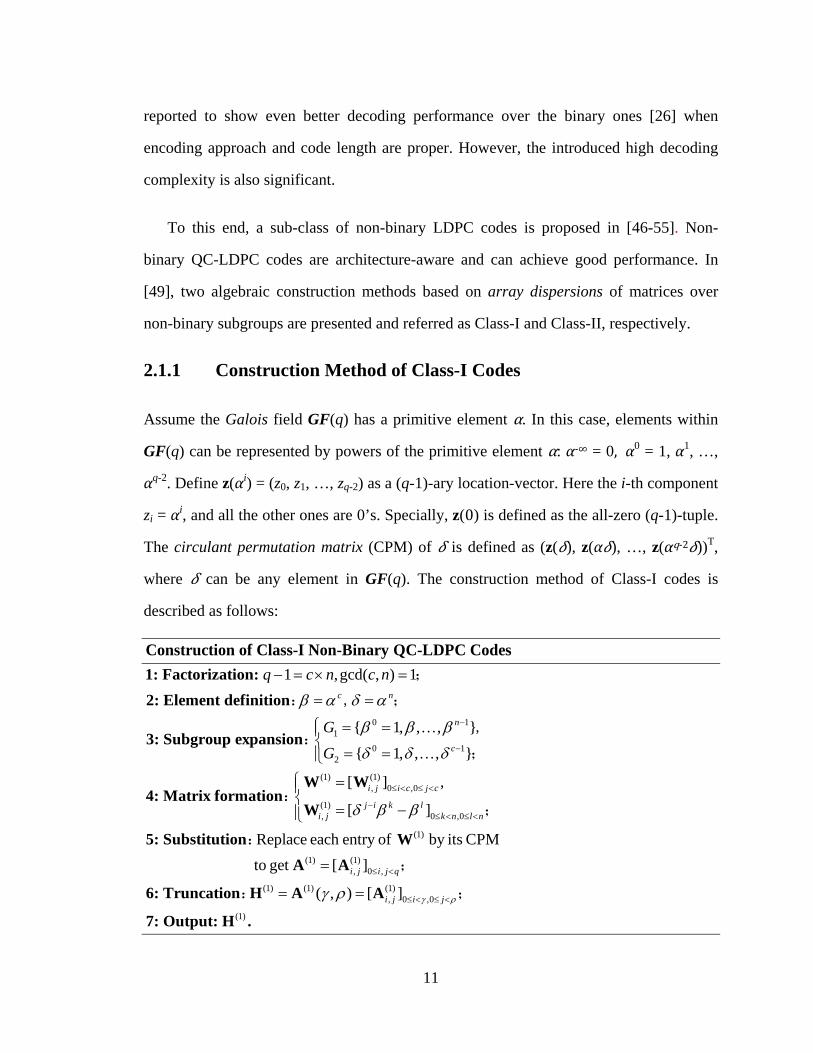
Construction Method of Class-I Codes ................................................. 11 2.1.1
Construction Method of Class-II Codes ............................................... 12 2.1.2
Prior Works on Non-Binary LDPC Decoders .............................................. 12 2.2
Decoding Algorithms for Non-Binary LDPC Codes ............................ 12 2.2.1
Existing Non-Binary LDPC Decoder Architectures ............................. 13 2.2.2
Geometry Properties of Non-Binary QC-LDPC Codes ................................ 14 2.3
Shifting Properties of Class-I Codes ..................................................... 15 2.3.1
Symmetry Properties of Class-II Codes ................................................ 16 2.3.2
Layer Partition Choice for Layered Decoding Algorithm ............................ 21 2.4

vi
Review of Layered Decoding Algorithm .............................................. 21 2.4.1
Layer Partition and Related Decoding Performances ........................... 22 2.4.2
A Reduced-Complexity Decoder Architecture ............................................. 23 2.5
Overall Architecture of Reduced-Complexity Decoder ....................... 24 2.5.1
Algorithm for Generating Local Switch Network of VNUs ................. 25 2.5.2
Architectures of VNUs’ Local Switch Network ................................... 30 2.5.3
Hardware Architectures of VNU Block ................................................ 33 2.5.4
Hardware Architectures of CNU Block ................................................ 34 2.5.5
Comparison with Prior Decoder Designs ..................................................... 40 2.6
Conclusion .................................................................................................... 45 2.7
............................... 46 Chapter 3 Low-Latency Sequential SC Polar Decoder
Introduction ................................................................................................... 46 3.1
SC Decoding Algorithm ....................................................................... 48 3.1.1
SC Decoding Algorithm in Logarithm Domain .................................... 50 3.1.2
Min-Sum SC Decoding Algorithm ....................................................... 51 3.1.3
Prior Works on SC Polar Decoder Designs .................................................. 52 3.2
DFG Analysis of the SC Polar Decoder ....................................................... 54 3.3
DFG Construction for the SC Polar Decoder ....................................... 54 3.3.1
DFG with Pre-Computation Look-Ahead Techniques ......................... 58 3.3.2
Pipelined Tree Decoder Architecture ............................................................ 60 3.4
Complete SC Tree Decoder Architecture Design ................................. 60 3.4.1
Architecture of Type I PE ..................................................................... 61 3.4.2
Architecture of Type II PE .................................................................... 62 3.4.3
Architecture of the Feedback Part ......................................................... 63 3.4.4

vii
Selecting Signals for De-/Multiplexers ................................................. 67 3.4.5
Pre-Computation Look-Ahead Sequential Decoder ..................................... 69 3.5
Architecture of the Revised Type I PE ................................................. 70 3.5.1
Architecture of the Merged PE ............................................................. 73 3.5.2
Decoder Architecture Construction ...................................................... 74 3.5.3
Architecture of the Revised Feedback Part ........................................... 75 3.5.4
Comparison of Latency and Hardware ......................................................... 78 3.6
Conclusion .................................................................................................... 81 3.7
.................... 82 Chapter 4 High-Throughput Interleaved SC Polar Decoders
Introduction ................................................................................................... 82 4.1
3-Overlapped SC Polar Decoder Example ................................................... 84 4.2
3-Overlapped Decoding Schedule ........................................................ 84 4.2.1
3-Overlapped SC Decoder Architecture ............................................... 85 4.2.2
Properties of Overlapped SC Decoder Architectures ................................... 86 4.3
The Construction Approach with Folding Technique .................................. 91 4.4
Preliminaries of Folding Transformation Technique ............................ 92 4.4.1
Previous Decoders with Folding Transformation Technique ............... 93 4.4.2
The Parallel Pre-Computation Look-Ahead Decoder ................................... 96 4.5
Comparison with Other Works ................................................................... 102 4.6
Conclusion .................................................................................................. 105 4.7
................................... 106 Chapter 5 Design of Simplified SC Polar Decoders
Introduction ................................................................................................. 106 5.1
Review of the SSC Algorithm .................................................................... 108 5.2
Tree Representation of the SC Decoding Algorithm .......................... 108 5.2.1
viii
The SSC Decoding Algorithm ............................................................ 111 5.2.2
The Latency Analysis of the SSC Decoder ................................................. 113 5.3
A Simple Example .............................................................................. 113 5.3.1
Latency Analysis for the General Code Length .................................. 116 5.3.2
Proposed SSC Decoder Architecture .......................................................... 119 5.4
DFG Analysis of the SSC Decoding Process ..................................... 119 5.4.1
The SSC Decoder Architecture Design .............................................. 119 5.4.2
Pre-Computation Look-Ahead SSC Polar Decoder .................................... 122 5.5
Look-Ahead SSC Polar Decoder Architecture ................................... 122 5.5.1
Latency of the Look-Ahead SSC Polar Decoder ................................ 123 5.5.2
Latency and Complexity Comparison ........................................................ 125 5.6
Conclusion .................................................................................................. 127 5.7
.......................... 129 Chapter 6 Conclusions and Future Research Directions
Conclusions ................................................................................................. 129 6.1
Non-Binary LDPC Decoders with Efficient Networks ...................... 130 6.1.1
Low-Latency Sequential SC Polar Decoder ....................................... 130 6.1.2
High-Throughput SC Polar Decoder Architectures ............................ 131 6.1.3
Design of Simplified SC Polar Decoders ............................................ 132 6.1.4
Future Research Directions ......................................................................... 133 6.2
Switch Networks for Other Non-Binary QC-LDPC Codes ................ 133 6.2.1
Low-Latency Low-Complexity CNU Architectures .......................... 135 6.2.2
Chip Implementation of the Proposed Polar Decoders ....................... 135 6.2.3
List Decoder Architectures for Polar Codes ....................................... 135 6.2.4
Polar Decoders Using Belief Propagation Algorithm ......................... 136 6.2.5

ix
Bibliography .................................................................................................. 137

x
List of Tables Table 2.1 Proposed surjective function example for tF ′ . .......................................... 18
Table 2.2 Comparisons for different non-binary QC-LDPC code decoders. ............ 41
Table 3.1 Decoding schedule for 8-bit SC decoder. .................................................. 57
Table 3.2 8-bit pre-computation look-ahead decoding schedule. .............................. 59
Table 3.3 Calculation of switching time for mn. ........................................................ 68
Table 3.4 Select signals for 8-bit decoder example. .................................................. 69
Table 3.5 Truth table of both full adder and subtractor. ............................................ 71
Table 3.6 Revised calculation of switching time for mn. ........................................... 76
Table 3.7 Comparison for different polar decoder architectures. .............................. 79
Table 4.1 The TC 3-interleaved decoding schedule for 8-bit decoder. ..................... 84
Table 4.2 The TC 1-, 3-, and 7-interleaved decoding schedule for 8-bit decoder. .... 88
Table 4.3 The TC 3-, 5-, and 7-interleaved decoding schedule for 8-bit decoder. .... 90
Table 4.4 Number of active merged PEs for the original decoder. ............................ 97
Table 4.5 Control signals for the RC 2-interleaved decoder. .................................... 98
Table 4.6 Number of active merged PEs for RC 2-interleaved decoder. ................ 100
Table 4.7 Number of active merged PEs for RC 3-interleaved decoder. ................ 102
Table 4.8 Comparison between the two proposed works and others. ...................... 103
Table 4.9 The TC 2-interleaved decoding schedule for 8-bit decoder. ................... 104
Table 5.1 The SSC decoding schedule for the (8, 3) polar decoder. ....................... 116
Table 5.2 The SSC decoding schedule for the (8, 5) polar decoder. ....................... 118
Table 5.3 Pre-computation schedule for the (8, 3) decoder. .................................... 122
Table 5.4 Pre-computation schedule for the (8, 5) decoder. .................................... 124
Table 5.5 Comparison between the proposed SSC decoders and others. ................ 126

xi
Table 6.1 Summary of major non-binary QC-LDPC codes. ................................... 134

xii
List of Figures Figure 1.1 Subscribers with China Mobile of the year 2010 [2]. ................................ 2
Figure 1.2 Simple block diagram of modern communication systems. ....................... 3
Figure 2.1 Performances of codes with different surjective functions. ..................... 20
Figure 2.2 PER comparisons between different algorithms for a Class-I code. ........ 23
Figure 2.3 Block diagram of proposed layered non-binary QC-LDPC decoder. ...... 24
Figure 2.4 Layered decoding example of the 4-ary (9, 3) rate-⅓ Class-I code. ........ 28
Figure 2.5 Layered decoding example of the 4-ary (12, 6) rate-½ Class-II code. ..... 30
Figure 2.6 Local switch network of Class-I codes case. ............................................ 31
Figure 2.7 Local switch network of the Class-II code defined by Eq. (2-15). ........... 32
Figure 2.8 Hardware implementation of the variable node unit (VNU). ................... 33
Figure 2.9 Internal structure of generator for possible solution sequences. .............. 36
Figure 2.10 Data sorter structure with length of nm. .................................................. 38
Figure 2.11 Proposed CNU block architecture employing data sorter. ..................... 39
Figure 3.1 Channel polarization for binary erasure channel (BEC) of rate 0.5. ........ 47
Figure 3.2 Encoding operation of the 8-bit polar code [28]. ..................................... 48
Figure 3.3 SC decoding process of polar codes with length N = 8. ........................... 50
Figure 3.4 SC decoding process with new labels. ..................................................... 54
Figure 3.5 DFG for the 8-bit SC decoding process. .................................................. 55
Figure 3.6 Simplified DFG for 8-bit SC decoding process. ...................................... 56
Figure 3.7 Four loops of the simplified DFG. ........................................................... 57
Figure 3.8 A quantizer example for pre-computation look-ahead approach [99]. ..... 58
Figure 3.9 DFG for 8-bit pre-computation look-ahead SC decoding process. .......... 59
Figure 3.10 The 8-bit conventional tree decoder architecture. .................................. 60

xiii
Figure 3.11 Proposed Type I PE architecture. ........................................................... 61
Figure 3.12 Proposed architecture of Type II PE. ..................................................... 62
Figure 3.13 Proposed structure of the TtoS block. ..................................................... 62
Figure 3.14 Flow graph of feedback part for 8-point polar decoder. ........................ 63
Figure 3.15 Simplified flow graph of the proposed feedback part. ........................... 65
Figure 3.16 Pipelined feed-forward architecture for 8-bit feedback part. ................. 66
Figure 3.17 The 2-parallel version of the architecture in Figure 3.16. ...................... 66
Figure 3.18 Recursive construction of Un based on Un-1. .......................................... 67
Figure 3.19 The W-bit parallel adder-subtractor architecture. ................................... 70
Figure 3.20 Proposed 1-bit parallel adder-subtractor architectures. .......................... 72
Figure 3.21 The revised Type I PE architecture. ....................................................... 73
Figure 3.22 Proposed structure of the merged PE. .................................................... 73
Figure 3.23 8-bit pre-computation look-ahead polar decoder architecture. ............... 75
Figure 3.24 Revised recursive construction of Un based on Un-1. .............................. 76
Figure 3.25 Revised recursive construction of Un using the memory bank. .............. 77
Figure 4.1 The 8-bit TC 3-interleaved SC polar decoder. ......................................... 85
Figure 4.2 The RC 2-interleaved architecture for 8-bit polar decoder. ..................... 99
Figure 5.1 Tree representation of the 8-bit SC polar decoder. ................................. 108
Figure 5.2 Decoding process of the 8-bit SC decoder with tree representation. ..... 110
Figure 5.3 The revised tree representation of the 8-bit SC polar decoder. .............. 112
Figure 5.4 Conventional SC decoding process. ....................................................... 113
Figure 5.5 SSC decoding process of the (8, 3) polar code. ...................................... 114
Figure 5.6 Nodes categorization with circled binary trees. ..................................... 115
Figure 5.7 Sub-trees identification for an (8, 5) code example. .............................. 118
xiv
Figure 5.8 The DFG for the SSC decoding approach. ............................................. 119
Figure 5.9 The SSC decoder architecture for the (8, 3) codes. ................................ 120
Figure 5.10 The fully-pipelined implementation for 3F⊗ . ...................................... 121
Figure 5.11 Recursive construction of the fully-pipelined implementation. ........... 121
Figure 5.12 Pre-computation SSC decoder architecture for the (8, 3) polar codes. 123
Figure 5.13 The qualified mixed node for the (8, 3) code. ....................................... 124
Figure 5.14 The qualified mixed node for the (8, 5) code. ....................................... 125
Equation Chapter 1 Section 1

1
Chapter 1
Introduction
Introduction 1.1
Along with the emergence and rapid development of modern communication
technologies, people’s lives have been enormously changed by a list of new concepts
such as streaming media, cloud storage, smart phone, and so on. The corresponding
markets are huge and of great potential. Take the mobile phone market as an example.
China Mobile is the world's largest individual mobile operator by subscribers [1].
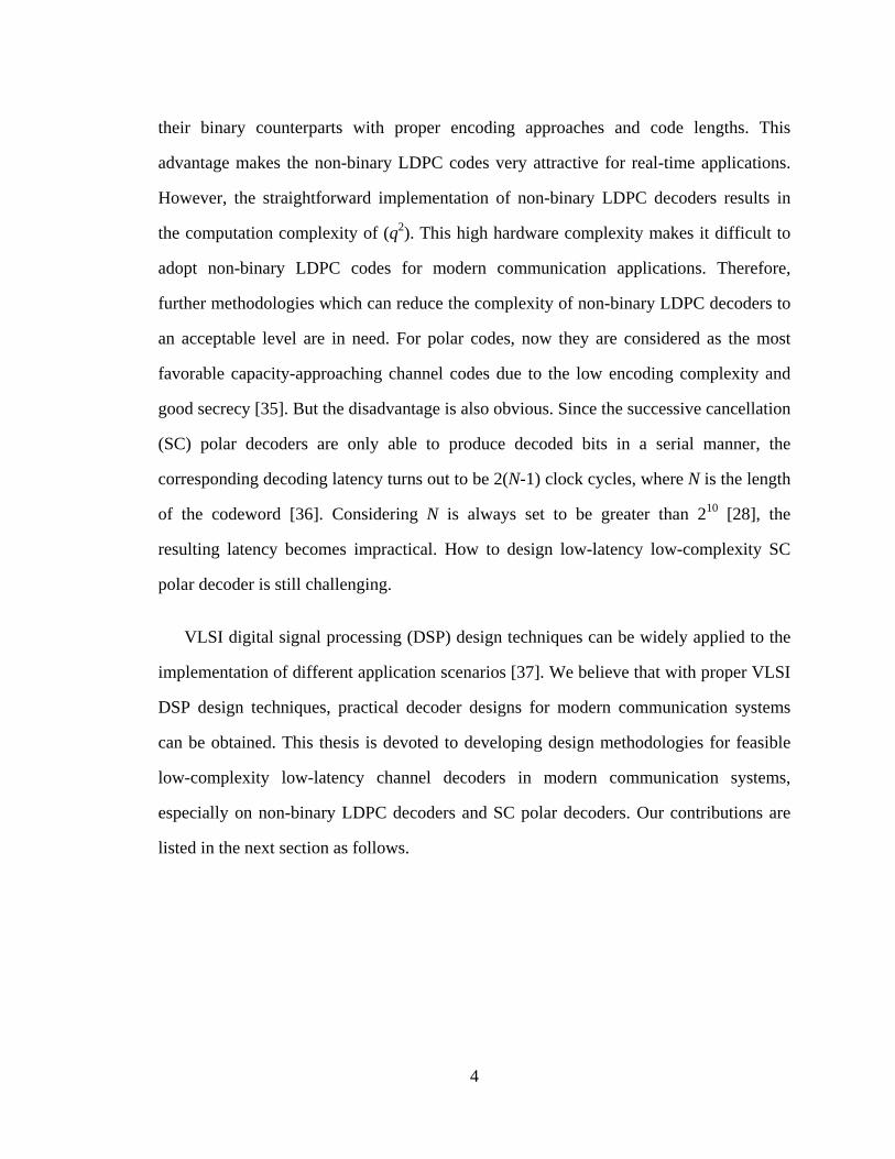
Illustrated in Figure 1.1, China Mobile has over 859 million mobile phone subscribers by
the end of the year 2010 [2]. By the end of 2009, more than 50 mobile operators have
over 10 million subscribers each. And more than 150 operators had at least one million
subscribers [2]. Not only the number of subscribers has expanded drastically, the data
transmission rate of a single mobile phone has increased a lot. The data-optimized 4th-
generation technologies such as the WiMAX standard [3] and the LTE standard [4] can
achieve up to 10-fold speed improvements over 3G technologies [5]. And still researchers
are now working towards the 5G systems [6], which would like to be implemented
around the year 2020 [7]. Therefore, it becomes very challenging for modern
communication systems to handle those increasing heavy tasks.

2
Figure 1.1 Subscribers with China Mobile of the year 2010 [2].
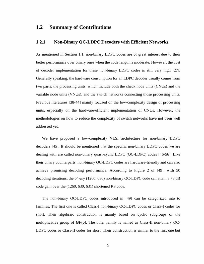
As illustrated in Figure 1.2, any modern communication system can be decomposed
into five parts, which are the source, the transmitter, the noisy channel, the receiver, and
the destination [8]. In order to protect the data transmitted over channels, we need to
effectively suppress the influence of the noise. Therefore, channel codes are always of
high necessity [9, 10]. Ever since the notation of channel capacity was defined by Claude
E. Shannon during World War II [11], channel codes have experienced a rapid
development [12]. From Gray codes [13], we had at the very beginning, nowadays we
have much more choices: Hamming codes [14], Reed-Solomon (RS) codes [15], Bose-
Chaudhuri-Hocquenghem (BCH) codes [16, 17], Turbo codes [18], fountain codes [19],
and low-density parity-check (LDPC) codes [20]. The history of channel codes is actually
the annals of modern communication systems’ development. This reminds us of the
emergence of Turbo codes, LDPC codes, and the iterative decoding methodology in
1990’s. These channel coding techniques have promoted the growth of modern
communication systems such as 10 Giga-bit/s Ethernet [21], Digital video broadcasting
[22], Wi-Fi [23], and 3G wireless communications [5]. On the other hand, the always-
756.6 760 776.9
786.5 795.9
805.3 814.1
823.1 833.3
842 850.3
859
700
720
740
760
780
800
820
840
860
880
Jan. Feb. Mar. Apr. May June July Aug. Sep. Oct. Nov. Dec.
Subscribers with China Mobile of year 2010 (million)

3
existing pressing need to develop “the next generation” communication systems drives
the development of channel codes move forward. Now, we are at the new turn again.
Here comes the first question: what error channel codes can we expect for the next
generation modern communication systems?
Figure 1.2 Simple block diagram of modern communication systems.
Aside from the issue of developing new channel codes, the efficient implementation
of corresponding decoders is of equal importance [24]. For modern communication
systems, to fulfill the long-distance high-quality information exchanges among a large
number of people, the corresponding decoders for channel codes are required to be fast,
portable, reliable, and safe [25]. This means that the channel decoder implementation
should be low-latency, low-complexity, low-error rate, and wiretap-free. Therefore, the
second question is: can we design low-complexity low-latency channel decoders to meet
the requirements of modern communication systems?
In order to answer the first question, recently two kinds of error correction codes have
been proposed by the coding society, which are non-binary LDPC codes [26, 27] and
polar codes [28-34], respectively. Compared with their binary counterparts, non-binary
LDPC codes are defined over finite field GF(q) with q>2. Previous literatures such as [26]
have shown that non-binary LDPC codes can show better decoding performance over
4
their binary counterparts with proper encoding approaches and code lengths. This
advantage makes the non-binary LDPC codes very attractive for real-time applications.
However, the straightforward implementation of non-binary LDPC decoders results in
the computation complexity of (q2). This high hardware complexity makes it difficult to
adopt non-binary LDPC codes for modern communication applications. Therefore,
further methodologies which can reduce the complexity of non-binary LDPC decoders to
an acceptable level are in need. For polar codes, now they are considered as the most
favorable capacity-approaching channel codes due to the low encoding complexity and
good secrecy [35]. But the disadvantage is also obvious. Since the successive cancellation
(SC) polar decoders are only able to produce decoded bits in a serial manner, the
corresponding decoding latency turns out to be 2(N-1) clock cycles, where N is the length
of the codeword [36]. Considering N is always set to be greater than 210 [28], the
resulting latency becomes impractical. How to design low-latency low-complexity SC
polar decoder is still challenging.
VLSI digital signal processing (DSP) design techniques can be widely applied to the
implementation of different application scenarios [37]. We believe that with proper VLSI
DSP design techniques, practical decoder designs for modern communication systems
can be obtained. This thesis is devoted to developing design methodologies for feasible
low-complexity low-latency channel decoders in modern communication systems,
especially on non-binary LDPC decoders and SC polar decoders. Our contributions are
listed in the next section as follows.
5
Summary of Contributions 1.2
Non-Binary QC-LDPC Decoders with Efficient Networks 1.2.1
As mentioned in Section 1.1, non-binary LDPC codes are of great interest due to their
better performance over binary ones when the code length is moderate. However, the cost
of decoder implementation for these non-binary LDPC codes is still very high [27].
Generally speaking, the hardware consumption for an LDPC decoder usually comes from
two parts: the processing units, which include both the check node units (CNUs) and the
variable node units (VNUs), and the switch networks connecting those processing units.
Previous literatures [38-44] mainly focused on the low-complexity design of processing
units, especially on the hardware-efficient implementation of CNUs. However, the
methodologies on how to reduce the complexity of switch networks have not been well
addressed yet.
We have proposed a low-complexity VLSI architecture for non-binary LDPC
decoders [45]. It should be mentioned that the specific non-binary LDPC codes we are
dealing with are called non-binary quasi-cyclic LDPC (QC-LDPC) codes [46-56]. Like
their binary counterparts, non-binary QC-LDPC codes are hardware-friendly and can also
achieve promising decoding performance. According to Figure 2 of [49], with 50
decoding iterations, the 64-ary (1260, 630) non-binary QC-LDPC code can attain 3.78 dB
code gain over the (1260, 630, 631) shortened RS code.
The non-binary QC-LDPC codes introduced in [49] can be categorized into to
families. The first one is called Class-I non-binary QC-LDPC codes or Class-I codes for
short. Their algebraic construction is mainly based on cyclic subgroups of the
multiplicative group of GF(q). The other family is named as Class-II non-binary QC-
LDPC codes or Class-II codes for short. Their construction is similar to the first one but

6
based on additive subgroups of the finite field. We will show that by exploiting the
intrinsic shifting and symmetry properties of non-binary QC-LDPC codes, significant
reduction of memory size and routing complexity can be achieved. These unique features
directly lead to two different network-efficient decoder architectures for Class-I and
Class-II codes, respectively.
Comparison results with the state-of-the-art designs show that for the code example
of the 64-ary (1260, 630) rate-0.5 Class-I code, the proposed scheme can save up to 70.6%
hardware required by the switch network, which demonstrates the efficiency of the
proposed design methodology. The proposed design for the 32-ary (992, 496) rate-0.5
Class-II code can achieve a 93.8% switch network complexity reduction compared with
conventional approaches. Those comparison results have demonstrated that the proposed
approaches are feasible and efficient.
Furthermore, we also try to reduce the hardware complexity of the CNUs. With the
help of a generator for possible solution sequences, both forward and backward steps can
be eliminated to offer processing convenience of the CNU blocks. Results show that the
proposed 32-ary (992, 496) rate-0.5 Class-II decoder can achieve 4.47 Mb/s decoding
throughput.
Low-Latency Successive Cancellation Polar Decoders 1.2.2
Polar codes have recently emerged as one of the most favorable capacity-achieving error
correction codes due to their low encoding and decoding complexity [28]. Polar codes are
constructed with a method called channel polarization to achieve the symmetric capacity
of any given binary-input discrete memoryless channel (B-DMC). It has been reported
that polar codes under list decoding with CRC are competitive with the best LDPC codes
at lengths as short as N = 211 [57].

7
However, because of the large code length required by practical applications (N ≥ 210),
the few existing SC decoder implementations still suffer from not only high hardware
cost but also long decoding latency. Therefore, SC polar decoders with less decoding
latency are required by modern communication systems. In this thesis, a data-flow graph
(DFG) for the SC decoder is derived. Based on the DFG analysis, a family of low-latency
SC polar decoders is derived formally [36, 58].
Low-Latency Sequential SC Polar Decoder
According to the DFG analysis, a low-latency sequential SC polar decoder architecture is
proposed to reduce the achievable minimum decoding latency. Pre-computation look-
ahead techniques are employed to halve the latency. The feedback part is presented for
the first time. Sub-structure sharing is used to design a merged processing element (PE)
for higher hardware utilization.
TC Interleaved SC Polar Decoder
In order to meet throughput requirements for a diverse set of application scenarios, a
systematic approach to construct different TC interleaved SC polar decoder architectures
is also presented. Compared with the conventional N-bit tree SC decoder, the proposed
TC interleaved architectures can achieve as high as (N-1) times speedup with only 50%
decoding latency and (N∙log2N)/2 merged PEs.
RC 2-Interleaved SC Polar Decoder
Another approach to meet the high-speed requirements for modern communication
system applications is introducing RC interleaved processing. However, the design of an
RC interleaved SC decoder is challenging due to the inherent serial decoding schedule.
Straightforward RC interleaved designs usually introduce significant decoding latency
8
overhead. To this end, in this paper a low-latency low-complexity RC 2-interleaved SC
decoder is proposed with the folding technique [59]. Compared with similar designs in
previous literatures, the proposed design can achieve 4 times speed-up while only
consumes similar hardware.
Simplified SC Polar Decoder Architecture 1.2.3
Although the low-latency SC polar decoder family could reduce the latency by 50%, we
believe that we do better. Recently, a low-latency decoding scheme referred as the
simplified successive cancellation (SSC) algorithm has been proposed for the decoding of
polar codes [60]. It is claimed that significant latency reduction is achieved over a wide
range of code rates. However, since this approach highly depends on the specific code it
is dealing with, the corresponding latency is not easy to predict.
In this thesis, we present the first systematic approach to formally derive the SSC
decoding latency for any given polar code [61]. The method to derive various SSC polar
decoder architectures for any specific code is also presented. Moreover, it is shown that
with the pre-computation technique, the decoding latency can be further reduced.
Similarly, the latency-reduced SSC decoder’s latency can also be calculated with a
simple equation. Compared with the state-of-the-art SC decoder designs, the two SSC
polar decoders can save up to 39.6% decoding latency with the same hardware cost.
Outline of the Thesis 1.3
The thesis is organized as follows. Chapter 2 gives a brief review of non-binary QC-
LDPC codes. Based on the geometry properties of Class-II and Class-II codes, two
different switch networks are proposed. A generator for possible solution sequences is
also introduced to further reduce the complexity of CNUs.
9
Chapter 3 introduces the design of low-latency sequential SC polar decoder. The
DFG of SC decoding process is proposed for the first time. Then the novel pre-
computation look-ahead SC decoder architecture is described in detail.
Chapter 4 presents two kinds of SC polar decoder architectures towards high-speed
applications. First, a systematic methodology for designing the TC interleaved SC polar
decoders is described. Afterwards, the RC 2-interleaved SC polar decoder architecture is
constructed based on the folding technique.
Chapter 5 proposes a method to determine the decoding latency of SSC algorithm. A
design approach for corresponding SSC polar decoder is given also.
Finally, Chapter 6 summarized of the contribution of the entire thesis and provides
future research directions.
Equation Chapter 2 Section 1

10
Chapter 2
Non-Binary LDPC Decoders with Efficient
Networks
In this chapter, we present two network-efficient decoder architectures for non-binary
QC-LDPC codes [45]. Section 2.1 provides a brief introduction of non-binary LDPC
codes and their sub-class, non-binary QC-LDPC codes. Section 2.2 briefly reviews prior
works on non-binary LDPC decoder designs. Section 2.3 investigates the geometry
properties of both Class-I and Class-II codes. Decoding schemes with different choices of
layers are evaluated in Section 2.4. Section 2.5 presents message passing schedules via
proposed networks and corresponding low complexity non-binary QC-LDPC decoder
architectures. The hardware cost estimations and comparisons are presented in Section
2.6. Section 2.7 concludes this chapter finally.
Introduction 2.1
Rediscovered by MacKay [62], binary LDPC codes have shown near-Shannon limit
performance [22, 63-66]. They have been extensively adopted in next-generation
communication system standards. Recently, LDPC codes over GF(q) with q>2 are
11
reported to show even better decoding performance over the binary ones [26] when
encoding approach and code length are proper. However, the introduced high decoding
complexity is also significant.
To this end, a sub-class of non-binary LDPC codes is proposed in [46-55]. Non-
binary QC-LDPC codes are architecture-aware and can achieve good performance. In
[49], two algebraic construction methods based on array dispersions of matrices over
non-binary subgroups are presented and referred as Class-I and Class-II, respectively.
Construction Method of Class-I Codes 2.1.1
Assume the Galois field GF(q) has a primitive element α. In this case, elements within
GF(q) can be represented by powers of the primitive element α: α-∞ = 0, α0 = 1, α1, …,
αq-2. Define z(αi) = (z0, z1, …, zq-2) as a (q-1)-ary location-vector. Here the i-th component
zi = αi, and all the other ones are 0’s. Specially, z(0) is defined as the all-zero (q-1)-tuple.
The circulant permutation matrix (CPM) of 𝛿 is defined as (z(𝛿), z(α𝛿), …, z(αq-2𝛿))T,
where 𝛿 can be any element in GF(q). The construction method of Class-I codes is
described as follows:
Construction of Class-I Non-Binary QC-LDPC Codes
0 11
0 12
(1) (1), 0 ,0
(1),
1 ,gcd( , ) 1
{ 1, , , }
{ 1, , , }
[ ] ,
[
1: Factorization: 2: Element definition
3: Subgroup expansion
W W4: Matrix formation
W
c n
n
c
i j i c j c
j i ki j
q c n c n
GG
β α δ α
β β β
δ δ δ
δ β β
−
−
≤ < ≤ <
−
− = × =
= =
= =
= =
=
= −
;
: , ;
,:
;
:0 ,0
(1)
(1) (1), 0 ,
(1) (1) (1), 0 ,0
(1)
]
Replace each entry of by its CPM to get [ ]
( , ) [ ]
5: Substitution WA A
6: Truncation H A A
7: Output: H .
lk n l n
i j i j q
i j i jγ ργ ρ
≤ < ≤ <
≤ <
≤ < ≤ <
=
= =
;
:
;
: ;

12
Construction Method of Class-II Codes 2.1.2
Using the additive subgroups instead of the cyclic ones, we have the construction method
of Class-II codes as follows.
Construction of Class-II Non-Binary QC-LDPC Codes
0 1 1
1 1
1 2 1
1 2 1
2 , 2 , and 2
{ , , , }
{ , , , }
{0, , , } spanned by
{0, , , } spanne
1: Factorization:
2: Elements definition
3: Subgroup expansion
t
m t
m m t t
tt
t t mm t
t t
m t
q c n
ff
F f
F
α α α
α α α
β β
δ δ −
−
−
+ −−
−
− −
= = =
′ =
′′ =′ ′=
′′ =
;
,:
;
,:
(2) (2), 0 ,
(2), 0 ,
(2)
(2) (2),
d by
[ ] ,
[( ) ( )]
Replace each entry of by its CPM to get [ ]
W W4: Matrix formation
W
5: Substitution WA A
m t
i j i j c
i j i j k l k l n
i j
f
δ δ β β
−
≤ <
≤ <
′′
=
= − + −
=
;
:;
:
0 ,
(2) (2) (2), 0 ,0
(2)
( , ) [ ]6: Truncation H A A
7: Output: H .
i j q
i j i jγ ργ ρ≤ <
≤ < ≤ <= =
;
: ;
Prior Works on Non-Binary LDPC Decoders 2.2
Much research has been carried out on non-binary LDPC decoder designs. A brief review
of previous works on non-binary LDPC decoding algorithms and decoder architectures is
given as follows.
Decoding Algorithms for Non-Binary LDPC Codes 2.2.1
The belief propagation (BP) algorithm is the locally optimal, yet the most complex,
iterative decoding algorithm of non-binary LDPC codes. Because the size of messages is
q, the straightforward implementation of BP algorithm has the complexity of (q2), which
is very high for hardware designers. To this end, several revised decoding algorithms
13
have been proposed. The log-domain decoding scheme [67] is mathematically equivalent
to the BP algorithm. It has shown advantages in both decoding complexity and numerical
robustness. By employing a p-dimensional two-point fast Fourier transform (FFT), the
computation complexity can be further reduced, where p = log2q. However, the FFT
algorithm is not suitable for the log domain. Then, a mixed-domain implementation has
been presented in [68]. In this algorithm, FFT operation is carried out in real-domain.
And the operations of CNU and VNU are carried out in log-domain. To implement the
exponential and logarithm computations, the look-up table (LUT) is employed for the
data conversion between log-domain and real-domain.
Unfortunately, for high-order field applications, all the above approaches are of
limited interests. This is because the number of LUT accesses grows with a complexity of
(qp) for a single message. To solve this problem, a complexity-reduced variant of the
Min-Sum (MS) decoding, called Extended Min-Sum (EMS), was proposed in [27, 69, 70].
In this algorithm, the CNUs only deal with a selective part of the incoming messages.
Moreover, some other low-complexity quasi-optimal iterative algorithms are proposed in
[71]. The Min-Max algorithm is the most attractive one of them. It reduces the total
number of operations with minimum decoding degradation.
Existing Non-Binary LDPC Decoder Architectures 2.2.2
Although in the past few years, the research on binary LDPC decoder design has
experienced a significant growth [72-74], very few publications on non-binary LDPC
decoder implementations have appeared. A straightforward implementation of the EMS
decoding algorithm was proposed in [41]. This is the first implementation of a non-binary
LDPC decoder with q≥64. [68] presented a mixed-domain non-binary LDPC decoder for
small codes. But the decoding throughput is only 1 Mb/s, which is not enough for modern
communication systems. In [42-44], several non-binary QC-LDPC decoder architectures

14
using semi-parallel processing scheme are proposed. Another two efficient non-binary
LDPC decoders have been proposed by [38] and [39]. Moreover, a flexible decoder
which is suitable for both binary and non-binary LDPC codes has been given in [40].
However, all those architectures suffer from high-complexity networks. This is because
they use either a bi-directional network or two full-size switch networks for shuffling and
reshuffling messages.
In this chapter, we present novel non-binary LDPC decoder architectures with both
high network efficiency and low hardware complexity. The layered decoding algorithm is
employed for the proposed decoders. By investigating the geometry properties of the
corresponding H matrices, two kinds of local switch networks for VNUs are introduced
for Class-I and Class-II codes, respectively. The proposed decoders are memory efficient,
highly parallel, and have low routing complexity. Comparison results have shown that
70.6% switch network hardware can be reduced compared with the state-of-the-art design
for decoding Class-I codes. And 93.8% can be reduced for Class-II decoders. Finally, by
uncovering the actual identity of parity check equations for different layers, low-
complexity CNUs are implemented.
Geometry Properties of Non-Binary QC-LDPC Codes 2.3
The parity-check matrix of non-binary QC-LDPC codes is simply composed of square
sub-matrices. [42-44] have addressed some straightforward properties of them. However,
for more efficient decoder architectures, more thorough investigations on the geometry
properties of the check matrix H are required now.

15
Shifting Properties of Class-I Codes 2.3.1
According to the construction method of Class-I codes, the identity of (1),Wi j and its
neighbor (1)( 1)mod ,( 1)modW i c j c− − can be verified by the following equation:
(1),
(( 1)mod ) (( 1)mod )
(1)( 1)mod ,( 1)mod
[ ]
[ ].
j i k li j
j c i c k l
i c j c
δ β β
δ β β
−
−
− −
= −
= −
=
- -
W
W (2-1)
Therefore, each row of the base matrix (1)W , except for the first row, is the 1-step right
cyclic-shift of the row above it. The first row is the 1-step right cyclic-shift of the last row.
Moreover, further exploitation of sub-matrix (1),Wi j can show that similar permutation
property holds at a lower level. Let (1)( , )( , )w i j k l be the entry of sub-matrix (1)
,Wi j located at
the k-th row and l-th column. The property can be expressed as follows,
(1)( , )( , )
( 1)mod ( 1)mod
(1)( , )(( 1)mod ,( 1)mod )
( ).
w
w
j i k li j k l
j i k n l n
i j k n l n
δ β β
β δ β β
β
−
− − −
− −
= −
= −
=
(2-2)
Note that except for the permutation operation, one multiplication with β is also required.
Combined with the definition of CPM, the geometry properties of Class-I codes can
be summarized as follows:
Proposition 1 The Class-I non-binary QC-LDPC codes satisfy the shifting properties at
three different levels:
1. The i-th row of the base matrix (1)W is exactly the 1-step right cyclic-shift of the [(i-
1)modc]-th row. Therefore, (1) (1), ( 1)mod ,( 1)modW Wi j i c j c− −= ;
2. The k-th row of the sub-matrix (1),Wi j is exactly the 1-step right cyclic-shift of the [(k-
1)modn]-th row multiplied by β, that is, (1) (1)( , )( , ) ( , )( 1, 1)i j k l i j k lβ − −=w w ..;
16
3. The m-th row of the CPM corresponding to (1)( , )( , )w i j k l is the 1-step right cyclic-shift of
the [(m-1)modn]-th row multiplied by α, which is given by the definition of CPM.
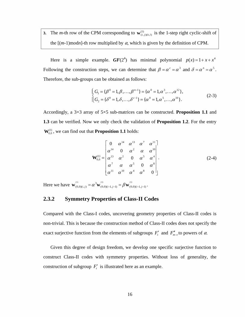
Here is a simple example. GF(24) has minimal polynomial 4( ) 1p x x x= + +
Following the construction steps, we can determine that 3cβ α α= = and 5nδ α α= = .
Therefore, the sub-groups can be obtained as follows:
0 1 0 3 121
0 1 0 5 102
{ 1, , , } { 1, , , },
{ 1, , , } { 1, , , }.
n
c
GG
β β β α α α
δ δ δ α α α
−
−
= = = =
= = = =
(2-3)
Accordingly, a 3×3 array of 5×5 sub-matrices can be constructed. Proposition 1.1 and
1.3 can be verified. Now we only check the validation of Proposition 1.2. For the entry (1)0,0W , we can find out that Proposition 1.1 holds:
14 13 7 11
14 2 10
(1) 13 2 5 40,0
7 5 8
11 10 4 8
00
.00
0
W
α α α αα α α αα α α αα α α αα α α α
=
(2-4)
Here we have (1) (1) (1)3(0,0)( , ) (0,0)( 1, 1) (0,0)( 1, 1)w w wi j i j i jα β− − − −= = .
Symmetry Properties of Class-II Codes 2.3.2
Compared with the Class-I codes, uncovering geometry properties of Class-II codes is
non-trivial. This is because the construction method of Class-II codes does not specify the
exact surjective function from the elements of subgroups tF ′ and m tF −′′ to powers of α.
Given this degree of design freedom, we develop one specific surjective function to
construct Class-II codes with symmetry properties. Without loss of generality, the
construction of subgroup tF ′ is illustrated here as an example.

17
Index Assignment of Surjective Function
0 0
Suppose , , with 0 ,
0, ,
1:
2: if then 3: elseif then 4: else5: for do 6: if then break7: else
p qm nm n
i jm m n n
l l
m n t
p q i jp q i j
l l l pm n i j
β α β α= =
= = ≤ <
< <> >
= + + ≤< <
∑ ∑ ;
;
;
;
then break8: endfor9: endif
l lm n i j> > ;
Table 2.1 denotes an example with t = 4. Here the minimal polynomial is given as 4( ) 1p x x x= + + . Based on the construction steps, the subgroup tF ′ is spanned by the t
elements within the set of 0 1 2 3{ , , , }tf α α α α′= . According to the proposed surjective
function, we can check that for any element iβ within sub-group tF ′ , the following
equation holds,
(2 1) 2 1t ti iβ β β
− − −+ = (2-5)
Similarly, for the other sub-group m tF −′′ , the same symmetry property holds,
2 1 2 1.m t m ti i
δ δ δ− −− − −+ = (2-6)
Therefore, the symmetry property for each sub-matrix of (2)W is given as follows,
(2) (2), 1, 1,W Wi j c j c i− − − −= (2-7)
which indicates that each sub-matrix (2),Wi j is identical with its mirror about the anti-
diagonal.
According to the construction method of non-binary QC-LDPC codes, every sub-
matrix (2),Wi j is also self-symmetric about its own anti-diagonal:
(2) (2)( , )( , ) ( , )( 1, 1) .w wi j k l i j n l n k− − − −= (2-8)

18
Table 2.1 Proposed surjective function example for tF ′ .
Polynomial form Power form Element 0 0 0β
1 1 1β
α α 2β
2α 2α 3β
3α 3α 4β
1 +α 4α 5β
1 + 2α 8α 6β
1 + 3α 14α 7β
α + 2α 5α 8β
α + 3α 9α 9β
2α + 3α 6α 10β
1 +α + 2α 10α 11β
1 +α + 3α 7α 12β
1 + 2α + 3α 13α 13β
α + 2α + 3α 11α 14β
1 +α + 2α + 3α 12α 15β
On the other hand, for Class-II codes, both the base matrix (2)W and its sub-matrix (2),Wi j are self-symmetric about their diagonals. This can be verified according to the 4th
step of the construction method of Class-II codes:
(2),
(2),
[( ) ( )]
[( ) ( )]
,
W
W
i j i j k l
j i k l
j i
δ δ β β
δ δ β β
= − + −
= − + −
=
(2-9)
(2)( , )( , )
(2)( , )( , )
( ) ( )
( ) ( )
.
w
w
i j k l i j k l
i j l k
i j l k
δ δ β β
δ δ β β
= − + −
= − + −
=
(2-10)
In what follows, we will summarize all the proposed geometry properties of Class-II
codes in Proposition 2:

19
Proposition 2 The Class-II non-binary QC-LDPC codes satisfy the geometry properties
at three different levels:
1. The base matrix (2)W is symmetric about its diagonal and anti-diagonal, i.e., (2) (2), ,W Wi j j i= and (2) (2)
, 1, 1W Wi j c j c i− − − −= ;
2. The sub-matrix (2),Wi j is also symmetric about its diagonal and anti-diagonal, i.e., we
have (2) (2)( , )( , ) ( , )( 1, 1)w wi j k l i j n l n k− − − −= and (2) (2)
( , )( , ) ( , )( , )w wi j k l i j l k= ;
3. Each row of one CPM (2)( , )( , )w i j k l is the right cyclic-shift of the row above it multiplied
by α and the first row is the right cyclic-shift of the last row multiplied by α.
Since Proposition 2.1 and 2.2 are similar, without loss of generality, we only give an
example of the latter one. Suppose t = 3 and the minimal polynomial 3( ) 1p x x x= + + .
According to the proposed index assignment scheme, (2)0,0W can be constructed as follows:
2 3 6 4 5
3 6 2 5 4
3 4 5 2 6
2 6 4 5 3(2)0,0 3 5 4 6 2
6 2 5 4 3
4 5 2 6 3
5 4 6 3 2
0 11 0
0 10 1
.1 0
1 00 11 0
W
α α α α α αα α α α α α
α α α α α αα α α α α αα α α α α αα α α α α αα α α α α αα α α α α α
=
(2-11)
It can be observed that (2)0,0W is symmetric about its diagonal and anti-diagonal. For
Proposition 2.3, which is similar to Proposition 2.1, similar conclusion can be drawn.

20
1.6 1.8 2.0 2.2 2.4 2.610-6
10-5
10-4
10-3
10-2
10-1
32-ary (992, 496) Class-II, EMS, Random 32-ary (992, 496) Class-II, EMS, Proposed
PER
SNR/dB
Figure 2.1 Performances of codes with different surjective functions.
We can also check that rows of the base matrix (2)W constructed according to the
proposed surjective function satisfy the α-multiplied row-column constraints [49].
Assume m = 5 and t = 2. With the code construction steps and surjective function, we can
construct a 32-ary (992, 496) rate-0.5 Class-II code. In order to guarantee the decoding
performance of codes generated with the proposed surjective function, another Class-II
code with random surjective function is employed for comparison. Figure 2.1 illustrates
the decoding performances of this code and its random counterpart over AWGN channel
with BPSK signaling. The conventional EMS decoding algorithm with maximum
iteration number of 10 is used for both codes.
Shown in Figure 2.1, it is observed that the packet error rate (PER) performance of
Class-II code with the proposed surjective function is similar as that of the one with
random scheme. Therefore, the introduced geometry properties do not affect the algebraic
architecture and the decoding advantage of Class-II codes.

21
Layer Partition Choice for Layered Decoding Algorithm 2.4
Review of Layered Decoding Algorithm 2.4.1
The layered decoding approach [75-78] partition the check matrix H into l layers:
10 1[ ].T T T T
H H H Hl−
= (2-12)
Each layer is associated with one super-code iC , and the original code C can be treated
as the intersection of all l super-codes [76]:
0 1 1.l−= C C C C (2-13)
It is required that the column weight of each layer is equal or less than 1.
The layered decoding message passing schedule with the Min-Max algorithm in the
k-th iteration for layer t can be formulated as follows:
Layered Decoding for Min-Max Algorithm
( )\( )
, ,( 1) ( 1),
, ,
( ) ( )\( )( | )
, , ,
( ) ( ) - ( )
( ) min ( max ( ))
( ) ( ) ( )
1: 2:
3: .
v v c vv
k t k t k tcv v cvk t k tcv cv va v c v
c a a
k t k t k tv cv cv
L a L a R aR a L a
L a L a R a
′ ′∈
− −
′ ′′∈∈ =
=
=
= +
;
;
Here, , ( )k tcvL a is the variable to check message from layer t to the next layer during the
k-th iteration which is associated with finite field element a. And , ( )k tcvR a is the check to
variable message. The message , ( )k tvL a is the LLRs from layer t to the next layer during
the k-th iteration. Define ( )c be the set of variable nodes participating in check node c,
and ( ) \ ( )c v be the set excluded the variable node v. ( | )vc a a= denotes the set of
finite sequences which satisfy check node c, given the value of the variable node v equals
a. As mentioned above, each layer carries out its own decoding process with both channel
inputs and the extrinsic output of last layer. Because of this novel updating schedule, the
layered decoding propagates much faster than the conventional ones such as the two-

22
phase message-passing (TPMP) decoding algorithm [26]. Therefore, compared with
conventional message passing algorithms, layered decoding performance is better within
the same number of decoding iterations.
Layer Partition and Related Decoding Performances 2.4.2
According to Proposition 1 and 2, nice algebraic construction enables both classes of
non-binary QC-LDPC codes accommodated with the layered decoding algorithm.
Inherently, their check matrix H can be split into layers. And each layer can naturally
serve as a super LDPC code. Actually, we have two layer partition options listed as
follows:
1. Choose each sub-block row of (1),Wi j or (2)
,Wi j as one layer, which consists of (q-1)
rows. This option is defined as the Layer-I choice;
2. Choose each row of CPM within (1)( , )( , )w i j k l or (2)
( , )( , )w i j k l as one layer, which consists of
only one row. This option is defined as the Layer-II choice.
It can be observed that the constraint of at most 1 column weight within each layer is
satisfied in both options. To demonstrate the advantages of the layered scheme for non-
binary QC-LDPC codes, one decoding example is given as follows. For a 64-ary (1260,
630) rate-0.5 Class-I code, performances of three decoding approaches are compared in
Figure 2.2. The maximum number of iterations is set to 10. Decoding performances of
the conventional Min-Max algorithm and Min-Max algorithm with two different layer
choices are illustrated. According to Figure 2.2, it can be seen that the layered decoding
variations can attain more than 0.08 dB decoding gain than the conventional Min-Max
algorithm. For the two different layer partition choices, the fewer rows in each layer, the
better performance can be achieved. This is because compared with the Layer-I choice,
more inter-layer extrinsic messages are utilized in each iteration of the Layer-II choice.

23
1.6 1.8 2.0 2.2 2.4 2.610-6
10-5
10-4
10-3
10-2
10-1
64-ary (1260, 630) Class-I, Min-Max 64-ary (1260, 630) Class-I, Min-Max Layer-I 64-ary (1260, 630) Class-I, Min-Max Layer-II
PER
SNR/dB
Figure 2.2 PER comparisons between different algorithms for a Class-I code.
A Reduced-Complexity Decoder Architecture 2.5
Although non-binary LDPC codes outperform their equivalent binary counterparts, the
efficient implementation of non-binary LDPC decoders still remains challenging. Since
the routing complexity and control memory size increase drastically with order of GF(q),
how to implement low-complexity switch network connecting various processing nodes
becomes a big problem. For the (u, v) non-binary QC-LDPC decoder, the straightforward
implementation requires ρp(q-1)γ-bit memory to store all the control signals. Here, u =
ρ(q-1) is the code length, and u-v = γ(q-1) is the number of check bits. In the following
part, we present a reduced-complexity decoder architecture based on the proposed
geometry properties of non-binary QC-LDPC codes. The decoder is suitable for both
serial and semi-parallel approaches. In addition, systematic algorithms to generate local
switch network of VNUs are proposed for both classes of non-binary QC-LDPC codes.

24
Overall Architecture of Reduced-Complexity Decoder 2.5.1
The overall block diagram of the proposed semi-parallel decoder is shown in Figure 2.3.
We assume the code-word length and layer height of H to be ρ(q-1) and w, respectively.
Illustrated in Figure 2.3, the proposed decoder architecture is composed of an array of
ρ(q-1) VNUs with a local switch network, a set of l CNUs, a global shuffle network, and
a permutation/de-permutation block which implements multiplication/division operation
in Galois fields. All l rows in each layer are updated in parallel, and a total of γ(q-1)/w = l
clock cycles are required per iteration.
De-/Perm
utation
Global Shuffle N
etwork
...
......
VNU0
... ...
VNU1
VNUu-1
CNU0
CNU1
CNUw-1
Local Switch N
etwork
...
Figure 2.3 Block diagram of proposed layered non-binary QC-LDPC decoder.
The most significant point of the global shuffle network is, it stays unchangeable in
the whole decoding process rather than being reconfigured for each layer. Once the parity
check matrix is determined, no more reconfiguring operation is required. The switch
network reconfiguration for the remaining layers can be eliminated by employing the
local switch network.

25
Algorithm for Generating Local Switch Network of VNUs 2.5.2
Local Switch Network for Class-I Codes Cases
With the shifting properties of Class-I codes in Proposition 1.2 and 1.3, the local switch
network now can be constructed based on a specific circulant permutation algorithm. It is
clear that Proposition 1.2 and 1.3 only differ in the value of the multiplicand (β or α).
Without loss of generality, here we chose the Layer-I decoding scheme as an example.
Intuitively, we can split the local switch network shuffling operation between two
layers into two steps. Mentioned previously, Eq. (2-2) can be employed to implement the
partition of Layer-I. In Step One, the double mod operation (( 1) mod , ( 1) mod )k n l n− − is
carried out. The multiplication with β, which introduces another permutation at the level
of CPM, is implemented in Step Two. The algorithm is given in detail:
Scheduling Algorithm for Local Shuffle Network - I
[ ( 1)]mod ( 1)
0 ( 1)Pass the result of last layer from
VNU to VNU
00 1
Step One
1: for all do2: 3: 4: endfor
Step Two
5: for all do6: for all do7:
i i q q
i qextrinsic
ij q
ρ
ρ
ρ
− − −
≤ < −
≤ <≤ < −
( 1) ( 1) ( )mod( 1)
Pass the result of last layer from VNU to VNU
8: 9: endfor10: endfor
i q j i q j c q
extrinsic
− + − + − −
Proof. Assume the code length is ρ(q-1). Therefore, we need the same number of VNUs.
Indicated by Eq. (2-2), the interconnection among CNUs and VNUs of the last layer can
be reused by the current layer. That is, the extrinsic result of the last layer can simply be

26
shuffled among existing VNUs before decoding the current layer. More specifically,
since (1)( , )( , )w i j k l is associated with (1)
( , )(( 1)mod ,( 1)mod )w i j k n l n− − , and the row index modulation can
be eliminated if the decoding process is carried out layer by layer, it is only required to
assign the extrinsic result of VNUi to [ ( 1)]mod ( 1)VNU i q qρ− − − . Also be aware that the
jumping stride of Step One is q-1, which is exactly the size of CPM.
However, the two sub-matrices in Eq. (2-2) are actually not identical, because of the
multiplication operation. Therefore, another permutation step named Step Two is required.
According to the definition of CPM, the CPM of (1)( , )( , )w i j k l can be obtained as follows.
Firstly, we have to right cyclic shift the CPM of (1)( , )(( 1)mod ,( 1)mod )w i j k n l n− − by logαβ steps.
Then, we multiply the shifted CPM with β. It is Based on the construction method, we
know that,
log .c cαβ α β= ⇒ = (2-14)
Therefore, in Step Two an inner permutation with jumping stride of c is carried out. In
this way, we assign the extrinsic result of ( 1)VNUi q j− + to ( 1) ( )mod( 1)VNUi q j c q− + − − .∎
Take the layered decoding of the 4-ary (9, 3) rate-⅓ Class-I code shown in Figure 2.4
as an example. The factorization parameters are given as c = 1, n = 3. Therefore, we have
β = αc = α over GF(22). For instance, as shown in Figure 2.4, VNU7 is connected with
CNU0 during the 1st layer decoding, and with CNU1 during the 2nd layer decoding. On the
other hand, according to the decoding scheduling, the extrinsic result of VNU7 is first
passed to VNU4 (Step One), then to VNU3 (Step Two) after the 1st layer decoding. It is
similar for other VNUs. Also it is observed that rather than establishing a new switch
network for the 2nd layer, the extrinsic results of the 1st layer can be efficiently shuffled
perfectly with the help of the local switch network.

27
Considering both Step One and Step Two involve the circulant permutations, we can
further simplify the scheduling algorithm by removing redundant shifting operations. The
resulting new scheduling algorithm merges the former two steps into a single step. The
proof is given as follows:
Proof. Each VNU’s index can be rewritten in the form of i(q-1)+j, where 0≤i<ρ and
0≤j<q-1. Therefore, every VNU can be represented with a new notation of (i, j). During
Step One, whose jumping stride is q-1, the extrinsic result is transferred to the ((i-1)modn,
j) VNU. Thereafter, the message is shuffled to the ((i-1)modn, (j-c)mod(q-1)) VNU in
Step Two. That is, only one step is required to pass the extrinsic result of last layer from
( 1)VNUi q j− + to [( 1)mod ]( 1) ( )mod( 1)VNU i n q j c q− − + − − .∎
New Scheduling Algorithm for Local Shuffle Network - I
( 1) [( 1)mod ]( 1) ( )mod( 1)
00 1
Pass the result of last layer fromVNU to VNU
1: for all do2: for all do3: 4: 5: endfor6: en
i q j i n q j c q
ij q
extrinsic
ρ
− + − − + − −
≤ <≤ < −
dfor
For ease of explanation, the schedule shown in Figure 2.4 is employed as an example
again. The index of VNU7 can be changed into the new form (2, 1). Using the new
scheduling algorithm, we can easily find out that the destination index is (1, 0). Therefore,
the extrinsic message is transferred from VNU7 to VNU3 (1×3+0 = 3), which matches
our previous analysis perfectly.

28
CPM(0) CPM(α2) CPM(α)
CPM(α2) CPM(0) CPM(α0)
α2×β=α00×β=0
α×β=α2
VNU0 VNU1 VNU2 VNU3 VNU4 VNU5 VNU6 VNU7 VNU8
CNU0CNU1CNU2
CNU0CNU1CNU2
1st Layer
2nd Layer
non-zero entry
zero entry
Figure 2.4 Layered decoding example of the 4-ary (9, 3) rate-⅓ Class-I code.
Local Switch Network for Class-II Codes Cases
Similarly, the local switch network for Class-II codes can be implemented based on the
inherent symmetry properties in Proposition 2.2 and 2.3. At the same time, it is worth
noting that, indicated by Eq. (2-7)-(2-10), we only need to take care of the symmetry
execution rather than both symmetry and multiplication. The scheduling algorithm for
Class-II codes can be derived as follows,
Scheduling Algorithm for Local Shuffle Network - II
1, mod( 1)( )
0 , the beginning of decoding the th layer 0
0 1Pass result of VNU index
1: for all do2: for all do3: for all do4:
v i nq n i n
v l vi
j qρ
−− + +
< ≤≤ <
≤ < −
, mod( 1)( )to VNU index5:
6: endfor7: endfor8: endfor
v i n
j
q n i n j− + +
The INDEX(n) matrix is an n×n matrix defined as ( ), 0 ,0[ ]INDEX indexn
i j i n j n≤ < ≤ <= .
The entries of the first row of INDEX are determined by 0,index j j= as default. Other
entries can be derived from the index assignment of surjective function and symmetry
properties of Proposition 2.2 and 2.3. For instance, INDEX(4) is given as follows,

29
(4)
0 1 2 31 0 3 2
.2 3 0 13 2 1 0
INDEX
=
(2-15)
It is observed that the matrix INDEX(4) is symmetric about both its diagonal and anti-
diagonal. The entries on the diagonal are 0’s, and the entries on the anti-diagonal are all
3’s (= n-1). The last row (column) is the reverse-order version of the first row (column),
and vice versa. The proof is given as follows,
Proof. According to Eq. (2-8) and Eq. (2-10), the sub-matrix (2)( , )( , )w i j k l is identical to both
(2)( , )( 1, 1)w i j n l n k− − − − and (2)
( , )( , )w i j l k . Therefore, the interconnection among CNUs and VNUs of
the last layer is exactly the same as that of the current layer, and can be reused afterwards.
Indicated by Proposition 2, the index of destination VNU can be obtained by using
symmetry properties. Since there is no permutation for the very beginning row, the first
row of INDEX is set as an array of n elements from 0 to n-1. Each column is associated
with one specific VNU during a iteration. Since the dimension of INDEX is n, the same
mapping scheme based on INDEX is performed by every n VNUs. Therefore, a modulo
operation on the VNU index is required.∎
A simple example is employed to give a clear explanation. For the 4-ary (12, 6) rate-
½ Class-II code illustrated in Figure 2.5, the factorization parameters can be obtained by
choosing t = 1. Accordingly, c = 2m-t = 2, and n = 2t = 2 over GF(22). The subgroups are
1{0, } {0,1}tF β′= = and 1{0, } {0, }m tF δ α−′′ = = . Therefore, the index matrix INDEX(4) is
given as follows,
(2) 0 1.
1 0INDEX
=
(2-16)

30
CPM(0)
CPM(α0)
VNU0 VNU1 VNU2
CNU0CNU1CNU2
CNU0CNU1CNU2
non-zero entry
zero entry
INDEX(2) = 0
1
1
0CPM(α0)
CPM(0)
VNU3 VNU4 VNU5
CPM(α)
CPM(α2)
VNU6 VNU7 VNU8
1st Layer
2nd Layer
CPM(α2)
CPM(α)
VNU9 VNU10 VNU11
Figure 2.5 Layered decoding example of the 4-ary (12, 6) rate-½ Class-II code.
As illustrated in Figure 2.5, after the 1st layer decoding, the extrinsic message of 0VNU is
transferred according to the following direction:
0,0 1,03 ( 0) 0 3 ( 0) 0 3VNU VNU VNU .index index× + + × + +→ = (2-17)
For the other VNUs, similar permutations can be obtained accordingly. The permutations
are listed as follows,
VNU0⟶VNU3, VNU6⟶VNU9, VNU1⟶VNU4, VNU7⟶VNU10, VNU2⟶VNU5, VNU8⟶VNU11, VNU3⟶VNU0, VNU9⟶VNU6, VNU4⟶VNU1, VNU10⟶VNU7, VNU5⟶VNU2, VNU11⟶VNU8.
Architectures of VNUs’ Local Switch Network 2.5.3
Local Switch Network for Class-I Codes
It can be observed that the inter-layer message shuffle scheduling is irrelevant of the
current layer index. It means, no matter what number i is, the extrinsic message transfer
between the i-th layer and the (i+1)-th layer is exactly the same. Therefore, it can be
implemented with fixed interconnections. Before further decoding steps are carried out,
the intermediate results of VNUs are re-directed via the local switch network.

31
... ... ......
... .........
... ... ......
... .........
local switch network
VNU(q-1)-1VNU1VNU0 VNU2(q-1)-1VNUq-1 VNUn(q-1)-1VNU(n-1)(q-1)-1VNU(n-1)(q-1)VNU(q-1)+1
LLRs(q-1)-1LLRs1LLRs0 LLRs2(q-1)-1LLRsq-1 LLRsn(q-1)-1LLRs(n-1)(q-1)-1LLRs(n-1)(q-1)LLRs(q-1)+1
...
...
...
...
VNUρ(q-1)-1VNU(ρ-1)(q-1)-1VNU(ρ-1)(q-1)
LLRsρ(q-1)-1LLRs(ρ-1)(q-1)-1LLRs(ρ-1)(q-1)
...
...
...
...
...
...
...
...
... ...
Figure 2.6 Local switch network of Class-I codes case.
32
The architecture of the local switch network for Class-I codes is illustrated in Figure
2.6. A total of ρ(q-1) VNUs are employed and shuffling details of the first n(q-1) VNUs
are given. Rather than store all extrinsic results immediately, we only need to store the
shuffled LLRs output by the local switch network, which can be directly used by other
elements. Similar scheme is also employed by VNUs with indices from n(q-1) to ρ(q-1).
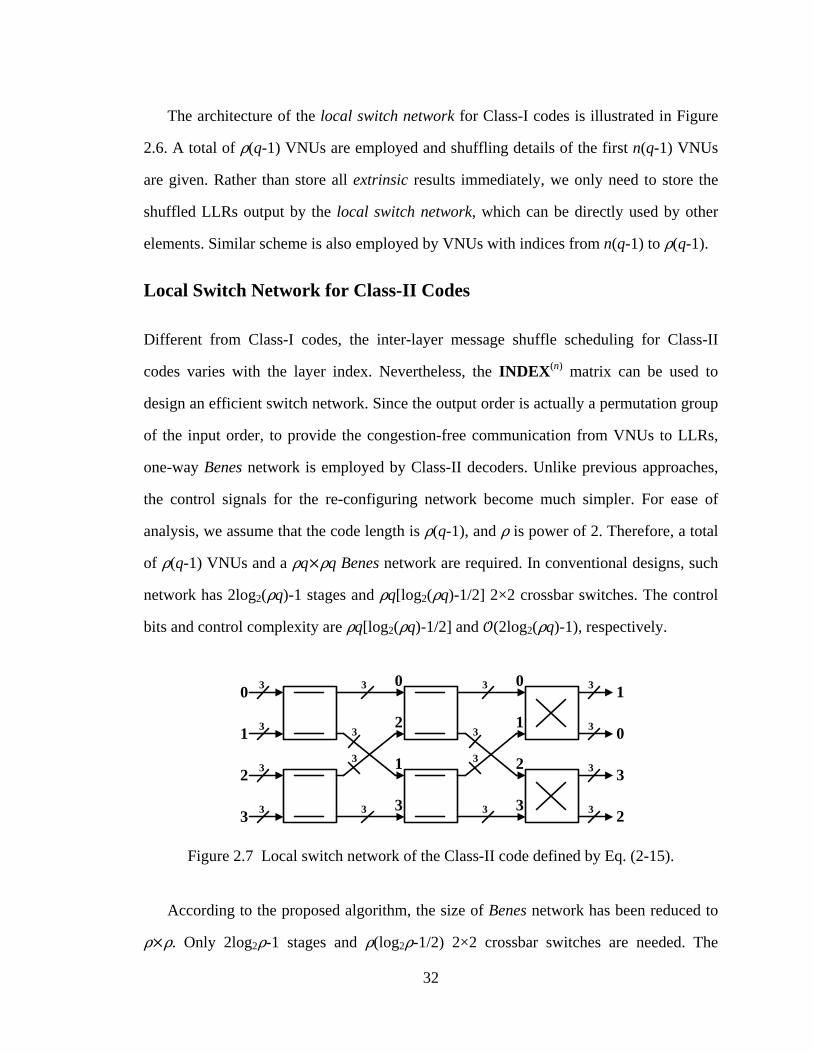
Local Switch Network for Class-II Codes
Different from Class-I codes, the inter-layer message shuffle scheduling for Class-II
codes varies with the layer index. Nevertheless, the INDEX(n) matrix can be used to
design an efficient switch network. Since the output order is actually a permutation group
of the input order, to provide the congestion-free communication from VNUs to LLRs,
one-way Benes network is employed by Class-II decoders. Unlike previous approaches,
the control signals for the re-configuring network become much simpler. For ease of
analysis, we assume that the code length is ρ(q-1), and ρ is power of 2. Therefore, a total
of ρ(q-1) VNUs and a ρq×ρq Benes network are required. In conventional designs, such
network has 2log2(ρq)-1 stages and ρq[log2(ρq)-1/2] 2×2 crossbar switches. The control
bits and control complexity are ρq[log2(ρq)-1/2] and 𝒪(2log2(ρq)-1), respectively.
0
1
2
3
1
0
3
2
0
2
1
3
0
1
2
3
3
3
3
3
3
3
3
3
3
3
3
3
3
3
3
3
Figure 2.7 Local switch network of the Class-II code defined by Eq. (2-15).
According to the proposed algorithm, the size of Benes network has been reduced to
ρ×ρ. Only 2log2ρ-1 stages and ρ(log2ρ-1/2) 2×2 crossbar switches are needed. The

33
control part has ρ(log2ρ-1/2) bits. Its complexity is (2log2ρ-1). In addition, the control
bits can be acquired by pre-computation with the aid of INDEX(n) matrix easily. For
instance, the local switch network for the example in Figure 2.7 is given as above.
We group VNUs with indices from i to i+2 and mark them with i, where i = 0, 1, 2,
and 3. Compared with conventional approaches, we succeed in taking the symmetry
properties into account. In the proposed designs, the main Benes network, the control
circuits, as well as the routing complexity are much simpler. Here, only 4 2×2 crossbar
switches are needed. It is clear that, the greater the parameter q is, the more hardware
reduction can be expected. When the value of ρ is not a power of 2, similar conflict-free
reconfigurable Clos network can be employed also. Please refer to [73, 79, 80] for more
details. To sum up, no matter what network is employed, the whole size can be reduced.
The low complexity advantage of the proposed method remains attractive.
Hardware Architectures of VNU Block 2.5.4
LLRs
,( )−k tvL 1
,k tcvR
VNUρ(q-1)-1
…
Output to CNUs
FIFO1
LLRs
,( )−k tvL 1
,k tcvR
VNU1
…FIFO0
LLRs
,( )−k tvL 1
,k tcvR
VNU0
…FIFOρ(q-1)-1
…
…
local switch network
( ),−k tcvR 1( ),−k t
cvR 1( ),−k tcvR 1
-- -
Figure 2.8 Hardware implementation of the variable node unit (VNU).

34
Figure 2.8 illustrates the straightforward architecture of a VNU, which is based on the
layered Min-Max decoding algorithm [75]. For each VNU, there is a FIFO employed. Its
depth is exactly the number of layers given by the partition scheme. In this manner, the
intrinsic messages for layer t during the k-th iteration can be correctly popped out for
layer t during the (k+1)-th iteration. Furthermore, based on the layered decoding scheme,
in each VNU a cascade of two adders are employed to update the variable to check
messages layer by layer. The output messages are then shuffled by the local switch
network, which will be slightly different from Class-I codes to Class-II codes, and stored
in the correctly arranged registers for the next layer decoding.
Hardware Architectures of CNU Block 2.5.5
The function of CNU block is to calculate the intrinsic message ( )cvR a , which is the
probability of check c being satisfied if the value of variable v (denoted as av) has been
determined as a and the value of any other variable v’ (denoted as av’) has an independent
distribution given by ( )cvL a′ . Here, variable v’ could be any variable connected with
check c rather than variable v. In binary cases, the possible choices for a are 1 or 0.
Therefore, whether the c-th check equation is satisfied or not can be easily determined by
checking the parity of 1’s in the c-th row of check matrix H. However, for non-binary
LDPC codes, provided the av is fixed at a, possible combinations which can make the
check equation true are not unique. In order to compute the value of ( )cvR a , we need to
traverse all the possible solution sequences for the equation below without missing a
single one, given av equals a.
( )\( )0.cv cv v
v c vh a h a′ ′
′∈
+ =∑
(2-18)
Referred as ( | )vc a a= , the set which contains all the possible sequences can be
found with an efficient recursive algorithm called forward-backward algorithm [26]. By
making the use of partial sums, this algorithm computes sum of the items prior to hcva

35
(denoted as σcv) and sum of items posterior to hcva (denoted as ρcv) in forward and
backward direction, respectively. If and only if the following equation holds, the check c
is satisfied.
.cv cv cvh aσ ρ+ = (2-19)
Though claimed to be efficient, the computation complexity of the forward-backward
approach is (q2). Mentioned previously, the CNU operation will become extraordinarily
computation intensive when the order of finite field q increases.
Check Equation Solution Sequences
Suppose the set ( | )vc a a= gives all the solution sequences for check c. That is, for any
sequence in , Eq. (2-18) holds. Two conclusions are stated as follows.
1. According to the commutativity of addition operation, any permutation of addends in
Eq. (2-18) will not affect the equality;
2. Also, if cvh and cvh ′ are changed with icvhα and i
cvhα ′ respectively, Eq. (2-18) will
still hold. Here, α is the primitive element of corresponding finite field GF(q) and i
can be any integer.
According to Proposition 1 and 2, it is known that for Layer-I partition scheme, each
layer is either the cyclic shift of previous row multiplied by β (Class-I codes) or the
symmetric version of previous row (Class-II codes). Also for Layer-II partition scheme,
no matter which class of non-binary QC-LDPC codes it belongs to, all q-1 entries of each
row are exactly 1-step right cyclic-shift of those in the above row multiplied by α.
Therefore, no matter what class the code is, no matter what layer partition is chosen, once
the set ( | )vc a a= which gives all the possible finite solution sequences for check c is
determined for the first layer, it will stay unchangeable for the remaining layers. As a
result, for the decoding process of these layers, the conventional forward-backward step

36
can be eliminated thereafter. Since the set of solution sequences is actually the same for
all CNUs, it is possible to pre-determine set ( | )vc a a= before the CNU decoding
process is carried out.
Generation for Finite Solution Sequences
In order to figure out the set of all finite solution sequences, a specific calculator has been
designed to search all the possible choices that satisfy the check equation. Illustrated in
Figure 2.9, a total of qρ-1 possible combinations are associated with the ρ-1 inputs of the
calculator. All inputs are multiplied with the non-zero entries lying in the first row of
check matrix H except for the last one (denoted as h00, h01, h02, …, h0(ρ-2)), respectively.
...
1/h0(ρ-1)
...
... .........
all p
ossi
ble
inpu
t co
mbi
natio
ns
h00
0iα
h01
1iα...
h0(ρ-3)
( 3)−i ρα
h0(ρ-2)
( 2 )−i ρα
implemented by permutations
ou
tput
to C
NU
s
Figure 2.9 Internal structure of generator for possible solution sequences.
The intermediate results are summed up then. For the selective Min-Max decoding
algorithm employed in this paper, the computation complexity can be further reduced
with the decrease of parameter nm. This is because both CNUs and VNUs only deal with
nm values rather than the values corresponding to all the elements in the finite field. An

37
additional, division step with parameter h0(ρ-1) is necessary to obtain the last required
element in the sequence. Suppose 0( 1)ih ρ α− = , in finite field GF(q) it always holds that
( 1) 1i q iα α − −⋅ = , the operation of division by h0(ρ-1) can then be simply implemented by
multiplication with its reciprocal 1 ( 1)0( 1)
q ih ρ α− − −− = . Furthermore, from the permutation
representation of finite field, all multiplication operations can be easily implemented with
permutations. After all input combinations have been simulated, all results as well as
their LLRs are output to CNUs for further use.
CNU Block Architecture Design
Usually, CNU blocks are the most complicated parts of the entire decoder. However, with
the nice geometry properties of non-binary QC-LDPC codes, the architecture of the CNU
block can be simplified. With the help of the proposed generator, all possible finite
solution combinations for a specific check node can be determined in advance. During
the check node process, we only need to compare the LLRs. In the Min-Max decoding
algorithm, the CNU process is aim to find the minimum value among infinite norms of all
possible check equation combinations given the corresponding variable node equals to a.
Here, a can be any element in a given finite field GF(q).
We can split the check node process into two steps. The first step is to find the
minimum value of all infinite norms if the variable node is fixed at a. In the second step,
we sort all possible a’s according to their likelihood values and pick up nm of them,
which have the most significant probabilities (LLRs). For ease of clarity, suppose the
check node degree is dc. We use the notation of ,{ ( )}k tcvR a⇐ to denote the insertion of
the LLR value , ( )k tcvR a into a pre-sorted LLR sequence. The CNU processing algorithm is
presented as follows,
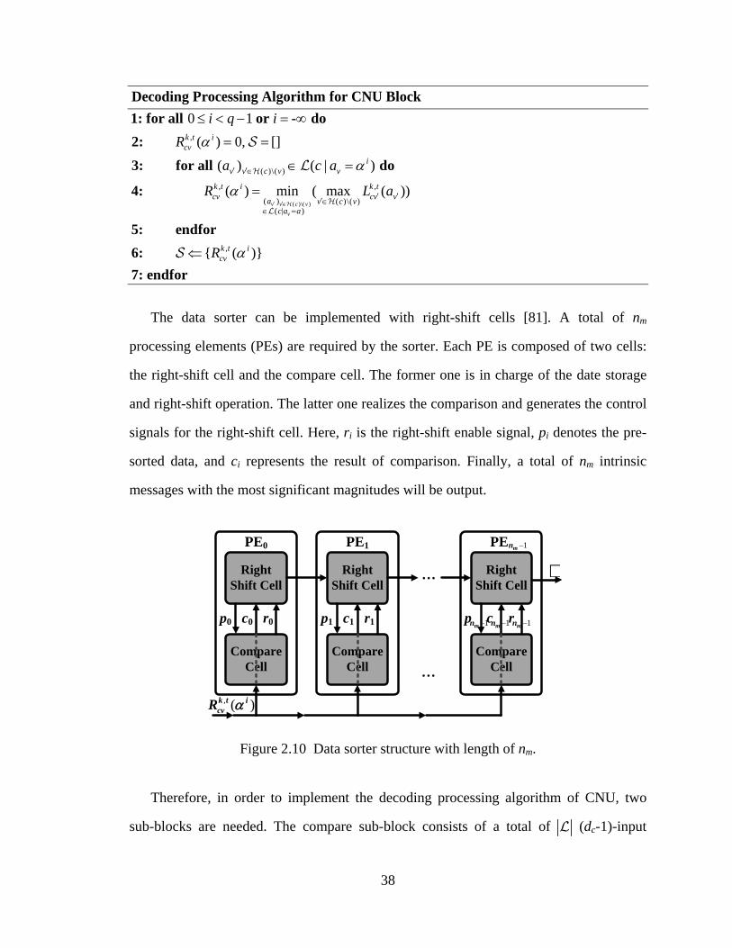
38
Decoding Processing Algorithm for CNU Block
( )\( )
,
( )\( )
, ,
( ) ( )\( )( | )
0 1( ) 0, []
( ) ( | )
( ) min ( max ( ))
1: for all or - do2: 3: for all do
4:
5:
v v c vv
k t icv
iv v c v v
k t i k tcv cv va v c v
c a a
i q iR
a c a
R L a
α
α
α′ ′∈
′ ′∈
′ ′′∈∈ =
≤ < − = ∞
= =
∈ =
=
,{ ( )} endfor
6: 7: endfor
k t icvR α⇐
The data sorter can be implemented with right-shift cells [81]. A total of nm
processing elements (PEs) are required by the sorter. Each PE is composed of two cells:
the right-shift cell and the compare cell. The former one is in charge of the date storage
and right-shift operation. The latter one realizes the comparison and generates the control
signals for the right-shift cell. Here, ri is the right-shift enable signal, pi denotes the pre-
sorted data, and ci represents the result of comparison. Finally, a total of nm intrinsic
messages with the most significant magnitudes will be output.
PE0
Compare Cell
Right Shift Cell
PE1
Compare Cell
Right Shift Cell
…
PE
Compare Cell
Right Shift Cell
1mn −
…
, ( )k t icvR α
r1r0 1mn −p0 c0 p1 c1 rp c 1mn −1mn −
Figure 2.10 Data sorter structure with length of nm.
Therefore, in order to implement the decoding processing algorithm of CNU, two
sub-blocks are needed. The compare sub-block consists of a total of (dc-1)-input

39
comparators and one ( -1)-input comparator, where is the cardinality of the set
( | )ivc a α= . The inputs of this sorter can be read off from the LUT of the finite
solution sequence generator. The input operation is achieved by a simple control unit
selecting αi. The result of , ( )k t icvR α is output to the sorter, which will pick up the nm most
significant ones, realign them in decreasing order, and output them to the v-th VNU for
further operations.
…
…
…
…
…
…
…
…
…
…
…
sorter
…
(dc-1)-input COMP|ℒ|-2
(dc-1)-input COMP0
(dc-1)-input COMP1
(dc-1)-input COMP|ℒ|-1
dc-1
dc-1
dc-1
dc-1
|ℒ|-input COMP
inpu
ts fr
om V
NU
s
, ( )k t icvR α to the v-th
VNU
(a) Concurrent version of CNU architecture.
sorter
…
, ( )k t icvR α to the v-th
VNU
……
(dc-1)-input COMP
dc-1
2-input COMP D
input from VNUs
(b) Simplified version of CNU architecture.
Figure 2.11 Proposed CNU block architecture employing data sorter.
The corresponding hardware architecture of the CNU block is illustrated in Figure
2.11 (a) as above. Moreover, the architecture in Figure 2.11 (a) can be further simplified

40
as shown in Figure 2.11 (b), where only one (dc-1)-input comparator is employed. For
both structures, given the value of iα , all the finite solution sequences are generated
by the module illustrated in Figure 2.9. In Figure 2.11 (a), all possible solutions are
processed in a parallel manner to select the required one. In the outer loop, only nm
intrinsic messages with the most significant magnitudes are chosen by the data sorter,
which is shown in Figure 2.10. In Figure 2.11 (b), the switch keeps open during the first
step. All the solution sequences are input in serial. Here we employ a 2-input comparator
with one delay element to generate LLR value of , ( )k t icvR α . In the outer loop, the switch is
closed and the sorter will output the nm most significant intrinsic messages.
Comparison with Prior Decoder Designs 2.6
In this section, we present the hardware complexity of the proposed two classes of non-
binary QC-LDPC decoder architectures and compare them with previous designs. The
decoding throughput of the proposed designs is also estimated at the end of this section.
Without loss of generality, it is assumed that the proposed (u, v) decoders employ the
Layer-I partition scheme. Therefore, a total of ρ(q-1) VNUs and q-1 CNUs are required.
It is assumed that a (bq, bf) uniform quantization scheme is employed, in which bq bits are
used for the entire message and bf bits are used for the fractional part. Table 2.2 lists the
comparison results of the decoder architectures for Class-I and Class-II codes,
respectively. For each decoder, both versions with specific and configurable shuffle
networks have been taken into account. The former version is designed for certain
specific code, whereas the latter version can be employed for decoding codes from the
same category. Design details are depicted in terms of cost of processing units,
complexity of shuffle network, and consumption of finite solution sequence generator.

41
Table 2.2 Comparisons for different non-binary QC-LDPC code decoders.
Different designs Class-I decoder Class-II decoder [42]a [44]a [43]b [38]b Specific Flexible Specific Flexible Hardware cost of processing units
Number of CNUs q-1 q-1 3(q-1) q-1 3(q-1) <γ(q-1) Each CNU
Registers bq(nm+1) bq(nm+1) REGs 9300 2635 9300 37696 Comp.s nm+dc-1 nm+dc-1 XORs 20693 11284 20693 40036
Number of VNUs ρ(q-1) ρ(q-1) ρ(q-1) ρ(q-1) ρ(q-1) <ρ(q-1) Each VNU
Registers bq(γ+nm) bq(γ+nm) − − − bq(γ+nm) Adders 2 2 2
Total units
Registers (q-1)bq[γρ+(ρ+1)nm+1] (q-1)bq[γρ+(ρ+1)nm+1] REGs 39990 35810 39990 3639648 Comp.s (q-1)(nm+dc-1) (q-1)(nm+dc-1) XORs 75469 79388 75460 3723348 Adders 2ρ(q-1) 2ρ(q-1) MEMs 1181410 451760 935110 206×106
Complexity of shuffle network
Global network
Wires bqnm(q-1)dc bqnm(q-1)dc 3bqnm(q-1)dc 3bqnm(q-1)dc 3bqnm(q-1)dc γbq(q-1)dc De-MUX’s 0 (q-1)ρ 0 (q-1)ρ 3(q-1)ρ 3(q-1)ρ 3(q-1)ρ γ(q-1)ρ LUT bits 0 p(q-1)ρ 0 p(q-1)ρ p(q-1)[ρ+γ(γ-1)/2] p(q-1)(3ρ+γ-2) p(q-1)(3ρ+γ-2) ρp(q-1)γ
Local network
Wires bq(q-1)γ bq(q-1)γ − − − − Crossbars 0 ρ(log2ρ-1/2) − − − − LUT bits 0 (γρlog2ρ)/2 − − − −
Consumption of finite solution sequence generator LUT bits pdc pdc − − − −
Galois adders dc-2 dc-2 − − − − aBoth designs are for a 32-ary (837, 726) rate-0.85 Class-I code. bBoth designs are for a 32-ary (744, 653) rate-0.875 non-binary LDPC code.

42
For different versions of decoders, the architecture of CNU stays the same. Each
CNU requires bqnm registers as well as nm+dc-1 2-input comparators, of which bqnm
registers and nm 2-input comparators are required by the shift-register sorter. For the
VNU, besides bq(γ+nm) registers for the FIFO, another 2 adders are also required. The
global shuffle network connects VNUs with CNUs. Once established, this network would
not change throughout the entire decoding process. Therefore, bq(q-1)dc wires are
sufficient. Otherwise, for additional flexibility consideration, bq(q-1)ρ bits LUT and (q-
1)ρ de-MUX’s are needed. Because of the different algebraic construction schemes, the
local switch network varies from Class-I decoder to Class-II decoder. For Class-I decoder,
it is only required to connect all VNUs end to end with bq(q-1)ρ wires, no matter whether
the design is specific or configurable. However, for Class-II decoder, another LUT
containing γ×ρ elements and related crossbar switches are required. Each element can be
represented with log2ρ quantization bits. Since the LUT is symmetric with respected to
both its diagonal and anti-diagonal as indicated by Eq. (2-15), the memory size can be
further reduced by half. Therefore, only (γρlog2ρ)/2 bits LUT is required. For the finite
solution sequence generator, all multiplication operations are implemented with finite-
step permutation, which requires pdc bits of LUT. In addition, a total of dc-2 Galois field
adders are required as well.
In order to demonstrate the advantages of the proposed designs, comparisons between
the proposed works and state-of-the-art designs [38, 42-44] are carried out. According to
the comparison results in Table 2.2, it is observed that compared with the state-of-the-art
decoder designs, the proposed designs can greatly reduce the hardware complexity by
making use of the geometry properties of non-binary QC-LDPC codes. Based on the
design scheme of [38, 42-44], the programming information of shuffle network should be
pre-stored into ROM to guarantee the proper execution of the decoding. Since ROM is
non-volatile, it is not convenient to incorporate flexibility into corresponding decoder

43
designs. Also, the decoder proposed in [42-44] are suitable for Class-I codes only. For
code choices such as Class-II codes, a fully constructed global network, such as the one
proposed in [38], is required by those decoders. On the other hand, the design approach
proposed in this dissertation can be employed for both Class-I and Class-II codes.
For the proposed Class-I decoder architecture, only fixed wires are necessary. It
means that, by introducing the local switch network, all memories can be eliminated. If
we can use more de-MUX’s and LUT, the decoder will be capable of dealing with a class
of codes rather than a specific one. Even in this case, the proposed decoder architecture
still shows advantages in hardware complexity. Now, we employ the 64-ary (1260, 630)
rate-0.5 Class-I code as an example for a better demonstration. Here, we know q = 64, ρ
= 20, and γ = 10. Therefore, the proposed configurable Class-I decoder needs a total of
p(q-1)ρ = 5×(32-1)×20 = 3,100 bits LUT and (q-1)ρ = (32-1)×20 = 620 de-MUX’s.
However, its counterparts in [42-44] require 3 times the amount of wires and de-MUX’s,
and p(q-1)[ρ+γ(γ-1)/2] = 5×(32-1)×[20+10(10-1)/2] = 10,075 bits of LUT. The shuffle
network in [44] needs even more, that is, a total of p(q-1)(3ρ+γ-2) = 5×31×(3×20+10-2)
= 10,540 bits of LUT are required. Since a conventional shuffle network is employed by
the decoder proposed in [38], it not surprising that the highest complexity is required.
Although having more flexibility, the proposed shuffle network still achieves hardware
saving of 69.2%, 70.6%, and 66.7% (because the number of CNUs is only 3 in [38])
compared with prior works, respectively. For the proposed Class-II decoder design, we
fail to give one comparison with other literatures, because no hardware implementation
has been addressed by previous literatures. However, we can still derive the hardware
reduction compared with the conventional approach which stores all the permutation
information for each layer. For configurable version of the 32-ary (992, 496) rate-0.5
Class-II code decoder, the resulting hardware saving is

44
( 1) ( 1) 1 16 1 93.8%.( 1) 16
p q k p q kp q k kρ ρ
ρ− − − − −
= = ≈−
(2-20)
Although another ρ(log2ρ-1/2) = 32×(log232-1/2) = 144 crossbar switches and
(γρlog2ρ)/2 = (32×16×log232)/2 = 1,280 bits of LUT are required, the expense is
relatively low compared with its benefits introduced. All the above analysis is for the
proposed flexible decoders, for the specific ones, more hardware reduction can be
expected with a sacrifice of configurability.
For the design of CNU block, the forward and backward steps in [41] can be
eliminated as a result. Therefore, simple implementation of the proposed CNU
architecture is achieved. Take a 32-ary (837, 726) rate-0.85 Class-I code as an example, it
can be computed that only 85 registers and 572 equivalent XOR gates are required. This
design requires less hardware consumption compared with designs in [42] and [44] while
achieving the same critical path of 12 XOR gates. Here, all messages are quantized in 5
bits. In order to further meet the requirements of high speed applications, pipelines can be
inserted into the comparator network. The pipelined comparator network is able to
achieve critical path of 2 XOR gates with 125 more registers. If shorter latency is required,
the concurrent version of comparator network can be employed, which will reduce the
latency at the expense of larger area. In general, the throughput of an LDPC decoder can
be calculated as follows:
,avg
Throughput p u fT I× ×
=× (2-21)
where f is the clock frequency determined by the critical path, T is the number of clock
cycles required by one decoding iteration, and avgI is the average number of decoding
iterations to process one code-word. As an example, the throughput of the proposed 32-
ary (992, 496) rate-0.5 Class-II flexible decoder can be estimated as follows. With the
state-of-the-art technology, it is reasonable to assume that the executing frequency of the

45
decoder to be 150 MHz [44]. Also the maximum number of decoding iterations is set to
10, nm is chosen to be 16, and the timing margin is given as 100 ns. The number of clock
cycles required by each iteration is (32×32+16)×16 = 16,640. Hence, the resulting
throughput is 4.47 Mb/s. If codes with higher rate and CNUs with larger concurrent
number are employed, higher throughput can be expected.
Conclusion 2.7
In this chapter, new non-binary QC-LDPC decoder architectures have been presented by
exploiting the unique geometry properties of the check matrices of both Class-I and
Class-II non-binary LDPC codes. Examples of Class-I and Class-II decoders have
demonstrated that the proposed design approaches can lead to up to 70.6% and 93.8%
hardware reduction for the switch networks. Moreover, by introducing the generator for
possible solution sequences, the CNU process is further simplified as well. Systematic
analysis has shown that the proposed schemes can result in efficient decoder designs with
decoding throughput of 6.46 Mb/s.
Equation Chapter 3 Section 1
46
Chapter 3
Low-Latency Sequential SC Polar Decoder
This chapter is organized as follows. An introduction to the SC decoding algorithm and
its logarithm domain variants is provided in Section 3.1. Section 3.2 reviews the prior
works on this topic briefly. In Section 3.3, the DFG of the SC polar decoder is
constructed and analyzed [58]. To the best knowledge of the authors, the architecture of
the feedback part for the conventional SC tree decoder is presented [36] in Section 3.4.
Using the DFG, the pre-computation look-ahead SC decoder architecture [36] is derived
in Section 3.5. Performance estimation and comparison with the state-of-the-art designs
are presented in Section 3.6. Section 3.7 concludes the whole chapter.
Introduction 3.1
Introduced by Arıkan recently [28], polar codes are capable of achieving the symmetric
capacity I(W) of any given binary-input discrete memoryless channel (B-DMC) W, when
the code length N is considerable large. By recursively combining and splitting N copies
of the B-DMC, we obtain a set of N binary-input coordinate channels ( ){ }iNW (1 )i N≤ ≤ .
Among the N newly constructed channels, only those with the highest capacity are used

47
for data transmission. We refer inputs of these channels as information bits ( )u , and the
set of corresponding indices as . The inputs of the other channels are denoted as frozen
bits ( )cu
, and those channels’ indices make up the set c. A common used example is
illustrated in Figure 3.1 [28], where the channel polarization phenomenon is quite
obvious.
Figure 3.1 Channel polarization for binary erasure channel (BEC) of rate 0.5.
Compared to the well-known Turbo codes [82-84] and LDPC codes [20, 85, 86],
polar codes are considered as the first codes that provably achieve the capacity for a
fairly wide array of channels. Also it is claimed that the encoding and decoding of polar
codes are of low complexity. These advantages make polar codes very attractive for real-
life communication applications.
Suppose 1Nx and 1
Nu are the input vector and encoded vector, respectively. NG is the
generator matrix. The encoding process of polar codes can be demonstrated with the
following Eq. (3-1):
1 1 ,N N N NN N Nx u G B F F B⊗ ⊗= = = (3-1)
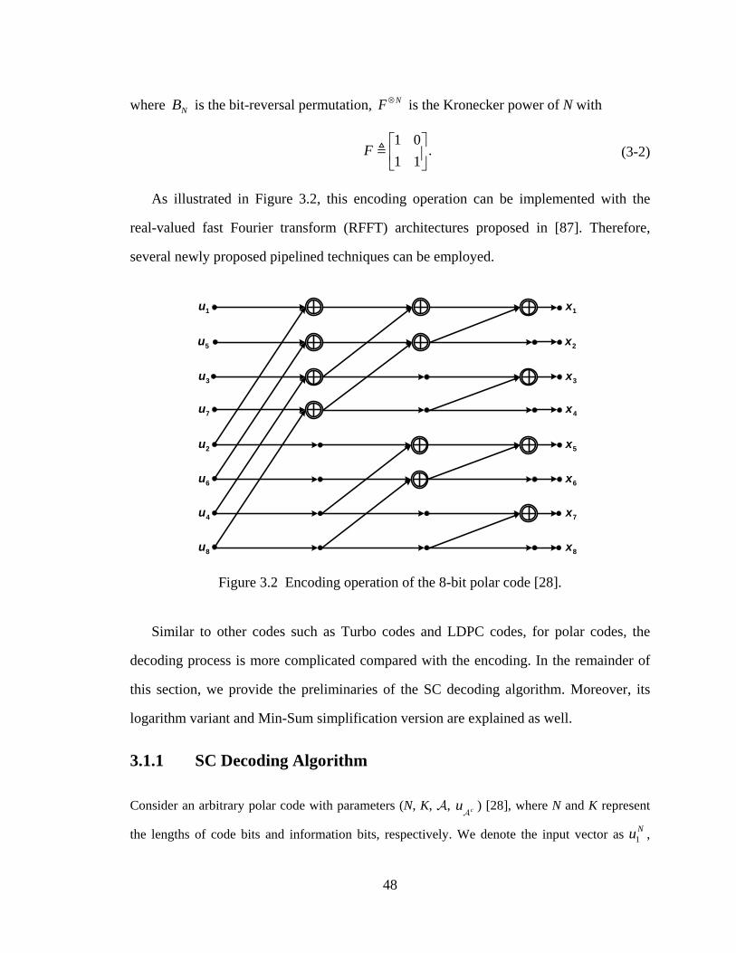
48
where NB is the bit-reversal permutation, NF⊗ is the Kronecker power of N with
1 0.
1 1F
(3-2)
As illustrated in Figure 3.2, this encoding operation can be implemented with the
real-valued fast Fourier transform (RFFT) architectures proposed in [87]. Therefore,
several newly proposed pipelined techniques can be employed.
u1
u5
u3
u7
u2
u6
u4
u8
x1
x2
x3
x4
x5
x6
x7
x8
Figure 3.2 Encoding operation of the 8-bit polar code [28].
Similar to other codes such as Turbo codes and LDPC codes, for polar codes, the
decoding process is more complicated compared with the encoding. In the remainder of
this section, we provide the preliminaries of the SC decoding algorithm. Moreover, its
logarithm variant and Min-Sum simplification version are explained as well.
SC Decoding Algorithm 3.1.1
Consider an arbitrary polar code with parameters (N, K, , cu
) [28], where N and K represent
the lengths of code bits and information bits, respectively. We denote the input vector as 1Nu ,
49
which consists of a random part u and a frozen part cu
. The corresponding output vector
through channel WN is 1Ny with conditional probability 1 1( | )N N
NW y u . The likelihood ratio (LR)
is defined as,
( ) 1( ) 1 1 1
1 1 ( ) 11 1
ˆ( , | 0)ˆ( , ) .ˆ( , |1)
i N ii N i N
N i N iN
W y uL y uW y u
−−
− (3-3)
In order to finish the decoding procedure, we are required to calculate the values of ( ) 1
1 1( , )i N iNL y u − for all 1 i N≤ ≤ . The detailed calculations can be done by applying the
following two equations recursively.
2 1
(2 ) 2 11 1
ˆ1 2( ) 2 2 2 2 2 ( ) 2 22 1 1, 1, 2 2 1 1,
ˆ( , )ˆ ˆ ˆ( , )] ( , ),=[ i
i N iN
ui N i i i N iN o e N N e
L y u
L y u u L y u−
−
−− − −+⊕ ⋅
(3-4)
(2 1) 2 2
1 1( ) 2 2 2 2 2 ( ) 2 2
2 1 1, 1, 2 2 1 1,( ) 2 2 2 2 2 ( ) 2 2
2 1 1, 1, 2 2 1 1,
ˆ( , )ˆ ˆ ˆ( , ) ( , ) 1
.ˆ ˆ ˆ( , ) ( , )
-
=+
i N iN
i N i i i N iN o e N N e
i N i i i N iN o e N N e
L y uL y u u L y uL y u u L y u
−
− − −+
− − −+
⊕ +
⊕ (3-5)
It can be observed that the calculation of ( ) 11 1( , )i N i
NL y u − depends on the estimate of the
previous bit, from which the SC decoding algorithm is named. After we have got all the
values of ( ) 11 1( , )i N i
NL y u − for 1 i N≤ ≤ , we need to finish the last step of the entire
procedure. It is worth noting that if ci∈ , that is the corresponding bit is a frozen bit, the
value of ˆiu is simply assigned as zero. The decision scheme is given as follows:
A Posteriori Decision Scheme with Frozen Bits
( ) 11 1
ˆ
ˆ ˆ( , ) 1 0ˆ 1
1: if then 2: else3: if then 4: else 5: endif6: endif
ci i
i N iN i
i
i u u
L y u uu
−
∈
≥
= ;
= ;
=;

50
The decoding procedure of polar codes with N = 8 is illustrated in Figure 3.3, where
Type I and Type II processing elements (PEs) compute Eq. (3-4) and (3-5), respectively.
The red label attached to each PE indicates the index of clock cycle when the
corresponding PE is activated during the decoding process. It can be seen that the
maximum value of the labels is 14, which means a total of 14 clock cycles are required to
finish the SC decoding process for the 8-bit polar codes. This issue will be discussed
further in following sections.
( ) ( )L y11 1
( ) ( )L y11 2
( ) ( )L y11 3
( ) ( )L y11 4
( ) ( )L y11 5
( ) ( )L y11 6
( ) ( )L y11 7
( ) ( )L y11 8
( ) ( )1 88 1L y
( ) ˆ( , )5 8 48 1 1L y u
( ) ˆ( , )3 8 28 1 1L y u
( ) ˆ( , )7 8 68 1 1L y u
( ) ˆ( , )2 88 1 1L y u
( ) ˆ( , )6 8 58 1 1L y u
( ) ˆ( , )4 8 38 1 1L y u
( ) ˆ( , )8 8 78 1 1L y u
1
1
1
1
2
2
3
4
5
5
6
7
8
8
8
8
9
9
10
11
12
12
13
14
ˆ ˆ ˆ ˆu u u u+ + +1 2 3 4
ˆ ˆu u+3 4
ˆ ˆu u+2 4
u4 u6
u2
ˆ ˆu u+5 6
ˆ ˆu u+1 2
u7
u3
u5
u1
: Type I PE : Type II PE
Stage 3Stage 2Stage 1
Figure 3.3 SC decoding process of polar codes with length N = 8.
SC Decoding Algorithm in Logarithm Domain 3.1.2
Generally, for every decoding algorithm defined in real domain, its logarithm variant
always has advantages in terms of hardware utilization, computational complexity, and
numerical stability [88]. Therefore, compared with their real-domain counterparts, the
decoding algorithms defined upon logarithm-domain are more attractive to hardware
51
designers [89-91]. Similar to the approach addressed in [89], the SC algorithm dealing
with logarithm-likelihood ratio (LLR) was also mentioned in [92]. First, we define the
LLRs as follows:
( ) 1 ( ) 11 1 1 1ˆ ˆ( , ) ln ( , ).i N i i N i
N Ny u L y u− − (3-6)
Then, the previous real-domain Eq. (3-4) and (3-5) can then be rewritten as follows:
2 1
(2 ) 2 11 1
ˆ ( ) 2 2 2 2 2 ( ) 2 22 1 1, 1, 2 2 1 1,
ˆ( , )ˆ ˆ ˆ(-1) ( , ) ( , ),i
i N iN
u i N i i i N iN o e N N e
y u
y u u y u−
−
− − −+= ⊕ +
(3-7)
(2 1) 2 1
1 1( ) 2 2 2 2 2 ( ) 2 2
2 1 1, 1, 2 2 1 1,
ˆ( , )ˆ ˆ ˆ2 tanh{tanh[ ( , ) 2] tanh[ ( , ) 2]}.
-i N iN
i N i i i N iN o e N N e
y uar y u u y u
−
− − −+= ⊕ ⋅
(3-8)
Min-Sum SC Decoding Algorithm 3.1.3
Although the SC decoding algorithm in logarithm domain seems more hardware-friendly
compared with the real-domain one, there is still one problem. In order to implement the
hyperbolic tangent function and its inverse function in Eq. (3-8), a look-up table (LUT) of
large size is required. In the cases when code length N is considerable large, the hardware
consumption for the LUT would be very high. To this end, some sub-optimal algorithms
which can achieve better trade-off between decoding performance and hardware cost are
required as a result.
Note that in logarithm domain, for any variable x ≫ 1, then we have the following
approximation holds:
ln[cosh( )] ln 2.x x − (3-9)
Consequently, by applying the approximation, we reduce Eq. (3-8) to the Min-Sum
update rule, which is LUT free:

52
(2 1) 2 2 ( ) 2 2 2 2 2 ( ) 2 21 1 2 1 1, 1, 2 2 1 1,
( ) 2 2 2 2 2 ( ) 2 22 1 1, 1, 2 2 1 1,
( ) 2 2 2 2 2 ( )2 1 1, 1, 2 2 1
1ˆ ˆ ˆ ˆ( , ) ( , ) ( , )2
1 ˆ ˆ ˆ( , ) ( , )2
ˆ ˆ ˆsgn[ ( , )]sgn[ ( ,
-i N i i N i i i N iN N o e N N e
i N i i i N iN o e N N e
i N i i i NN o e N N
y u y u u y u
y u u y u
y u u y
− − − −+
− − −+
− −+
⋅ ⊕ + −
⋅ ⊕ −
= ⊕
2 21,
( ) 2 2 2 2 2 ( ) 2 22 1 1, 1, 2 2 1 1,
)]
ˆ ˆ ˆmin[ ( , ) , ( , ) ].
ie
i N i i i N iN o e N N e
u
y u u y u
−
− − −+
⋅
⊕
(3-10)
Simulation results have demonstrated that the Min-Sum SC decoding algorithm only
suffers from little performance degradation than the optimal one while achieving high
hardware utilization [92]. This makes Min-Sum SC decoding algorithm very attractive
for VLSI implementation. Therefore, in this chapter we will focus our discussion of the
polar decoder design on this sub-optimal algorithm only.
Prior Works on SC Polar Decoder Designs 3.2
Most of the research on polar codes has been focused on code performance rather than
the design of high efficiency decoder architectures. Shown in [28], the straightforward
polar decoder implementation using successive cancellation (SC) algorithm results in the
complexity of 𝒪(Nlog2N). Several design examples based on belief propagation (BP)
algorithm were also proposed in [28] and [34, 93]. However, due to its lower complexity
compared with the BP algorithm, the SC approach appears more attractive for hardware
implementation. Reduced SC decoders with complexity of 𝒪(N) were presented in [92]
and [94]. However, to decode a polar code with length of N, 2(N-1) clock cycles are
required by the decoder. For real-time applications, in order to achieve the required
decoding performance, code length N higher than 210 is usually a necessity. Therefore,
the approach proposed in [92] and [94] requires long decoding latency for large N.
Another problem is that in each active stage of the decoder the highest hardware
utilization can be only 50%, which means half of the processing elements (PEs) are idle
at the same time. This is simply because the estimation of the current bit depends on the

53
value of the previous coded bit, which forces all coded bits to be output sequentially. A
latency-reduction approach called simplified SC decoding has been proposed in [60]
recently. Since this method is code-specific and highly influenced by the channel model,
it would not be discussed in this chapter. An empirical method to construct pre-
computation look-ahead decoding schedule for any polar codes was presented in [36] to
shorten the decoding latency by half. However, without investigating the inherent
properties of the decoder’s data-flow graph (DFG), this method cannot be generalized to
derive other decoder designs to meet different real-time application restrictions.
This chapter makes three contributions. First, a DFG is derived and analyzed for the
SC decoding process. According to the analysis result, validation of the empirical pre-
computation look-ahead approach in [36] is guaranteed. It is shown that the SC decoding
process can in fact be described by a multi-rate DFG [95, 96], whose iteration bound is
determined by the execution time of a single processing element (PE) only. Second,
based on the DFG analysis, we present a complete pipelined hardware architecture for the
conventional tree SC polar decoder for the first time. A new sub-block called the
feedback part is proposed to compute the 1-bit input signals for Type I processing
elements (PEs). We show that this sub-block can be constructed recursively. We also
give a systematic method to conveniently determine the select signals for de-
/multiplexers. The pre-computation look-ahead decoder can be easily constructed within
the new DFG context. It is demonstrated that compared with the architecture in [92], the
proposed low-latency architecture can halve the decoding latency with similar hardware
consumption. Comparison results show that the proposed pre-computation look-ahead
sequential decoder has the advantage in latency or throughput compared with the
conventional tree SC decoders.

54
DFG Analysis of the SC Polar Decoder 3.3
The DFG captures the data-driven property of DSP algorithms where any node can fire
whenever all the input data are available [37]. In a DFG, the nodes represent functions,
while the directed edges represent the data communications between nodes. Each edge
has a nonnegative number of delays associated with it [97]. In order to derive the pre-
computation look-ahead SC decoder architectures, we first consider construction of the
DFG of the SC polar decoder in this section.
DFG Construction for the SC Polar Decoder 3.3.1
In order to construct the DFG of the SC polar decoder, certain pre-processing is required.
Illustrated in Figure 3.4, each PE in the SC decoding process is marked with a new label
(red) for better identification.
( ) ( )L y11 1
( ) ( )L y11 2
( ) ( )L y11 3
( ) ( )L y11 4
( ) ( )L y11 5
( ) ( )L y11 6
( ) ( )L y11 7
( ) ( )L y11 8
( ) ( )1 88 1L y
( ) ˆ( , )5 8 48 1 1L y u
( ) ˆ( , )3 8 28 1 1L y u
( ) ˆ( , )7 8 68 1 1L y u
( ) ˆ( , )2 88 1 1L y u
( ) ˆ( , )6 8 58 1 1L y u
( ) ˆ( , )4 8 38 1 1L y u
( ) ˆ( , )8 8 78 1 1L y u
Stage 3Stage 2Stage 1
ˆ ˆ ˆ ˆu u u u+ + +1 2 3 4
ˆ ˆu u+3 4
ˆ ˆu u+2 4
u4 u6
u2
ˆ ˆu u+5 6
ˆ ˆu u+1 2
u7
u3
u5
u1
: Type I PE : Type II PE
A1
B1
A2
B2
A3
B3
A4
B4
C1
C3
D1
D3
C2
C4
D2
D4
E1
E3
E2
E4
F1
F3
F2
F4
Figure 3.4 SC decoding process with new labels.

55
According to the dependence relationship of each PE, the straightforward DFG can be
constructed as follows in Figure 3.5. The “D” represents a delay element. All output bits
are marked at the same clock cycle in which they are generated. By the way, it is worth to
point out that the proposed DFG can be partitioned into two identical parts as shown by
the dotted circles.
E1 F1 E2 F2
A1
A2
A3
A4
C1
C2
B1
B2
B3
B4
D1
D2
E3 F3 E4 F4
C3
C4
D3
D4
D
D
D
D
D
D
D
D
D
D
D
D
D
D
D
D D
D
D
D
D
D
D
D
D
D
D
D D
u1 u2 u3 u4 u5 u6 u7 u8
Figure 3.5 DFG for the 8-bit SC decoding process.
Since the PEs 1,2,3,4A are functionally identical, we can merge them together and
represent the merged one with A. Similar approaches can be applied to other PEs. After
merging all similar PEs together, we can derive a more compact version of DFG shown
in Figure 3.6. The red dash line indicates the flow of the entire decoding procedure,
which also corresponds to the decoding latency. The { }i affiliated to each switch means
the corresponding closure occurs during Clock Cycle 14n+i, where n≥0. The figures at
the input or output of each PE represent the number of samples consumed or produced by
an invocation of that PE [37].

56
A
B
C
D
E
F
D D
D
D
start
end
Stage 1 Stage 2 Stage 3
{1}
{8}
{2,9}
{5,12}
{3,6,10,13}
{4,7,11,14}
1
1
2 11
1
2
1
1
2
4
1
Figure 3.6 Simplified DFG for 8-bit SC decoding process.
According to the proposed DFG, it can be seen that during the entire decoding
process, PEs in Stage i will be activated 2i-1 times. Therefore, the decoding latency of 8-
bit SC polar decoder is 2×(22+21+20) = 14 clock cycles. More generally, with similar
DFGs we can further verify that the decoding latency should be
2 2log log1
1
2 12 2 2 2( 1),2 1
N Ni
iN−
=
−× = × = −
−∑ (3-11)
which matches with the empirical conclusion derived in [36]. Since the numbers at both
ends of an edge are different, the conventional SC polar decoder is actually a multi-rate
system rather than a single-rate system [98].
More importantly, the iteration bound of the DFG is always determined by the
processing time of one PE. The iteration bound is defined as the maximum loop bound.
The loop bound represents the lower bound on the loop computation time. In summary,
two properties of the DFG are stated as follows:
1. The decoding latency for an N-bit SC polar decoder equals 2(N-1) clock cycles;
2. The iteration bound of the DFG equals the processing time of a single PE.
Proof The proof of the first property is given by Eq. (3-11) already. For the second
property, the DFG in Figure 3.6 contains four loops (Figure 3.7), namely, the loops
57
1 2
3 4
, ,, .
l E F D E l F D E Fl E F B C E l F B C E F
= → → → = → → →= → → → → = → → → →
(3-12)
Suppose the processing time for each PE is T. The loop bounds for l1, l2, l3, and l4 are
3T/3 = T, 3T/3 = T, 4T/4 = T, and 4T/4 = T, respectively. Thus, the iteration bound is
3 3 4 43 3 4 4max{ , , , } .T T T TT T∞ = = (3-13)
Generally, in the DFG for the N-bit SC polar decoder, each loop has the same number
of PEs and delay elements. Hence, the iteration bound of the DFG equals the processing
time of a single PE.∎
(c)
E F B CD D D
D
(d)
F B C ED D D
D
(a)
E F DD D
D
(b)
F D ED D
D
Figure 3.7 Four loops of the simplified DFG.
For the ease of understanding, the corresponding decoding schedule for the 8-bit SC
decoder is shown in Table 3.1. C refers to the code-word which is being processed. Again,
similar to the proposed DFG, it is observed that the second half of the decoding schedule
is identical to the first half.
Table 3.1 Decoding schedule for 8-bit SC decoder.
Stage Clock cycle 1 2 3 4 5 6 7
1 C –– –– –– –– –– –– 2 –– C –– –– C –– –– 3 –– –– C C –– C C
Stage Clock cycle 8 9 10 11 12 13 14
1 C –– –– –– –– –– –– 2 –– C –– –– C –– –– 3 –– –– C C –– C C

58
We now can transform the proposed DFG in Figure 3.6 to achieve iteration bound
with lower decoding latency. This is addressed in the following sub-section.
DFG with Pre-Computation Look-Ahead Techniques 3.3.2
Pre-computation look-ahead approach is also referred to as parallel branch and delayed
decision approach [99]. This approach is often used to achieve faster processing rate
when the number of possible outputs is finite.
Therefore, we could always perform all possible calculations a priori, get all the
candidate results, and select the suitable one from the candidate pool thereafter. This
approach can save us more processing time. Figure 3.8 illustrates a simple example of a
first-order two-level quantizer loop [99]. Its pre-computation look-ahead reformulated
version is illustrated in (b) part of the same figure. According to the figure, we can see
that the latter one can potentially achieve faster speed.
b2
b1D
( )u n
( )nα
( )x n( )+x n 1
Q[∙]
(a) A first-order two-level quantizer loop.
q1[∙]
D
0
1
q1[∙]
b1b2
b1
b2
( )x n1
( )+x n1 1
( )nα( )u n
( )x n
(b) Its pre-computation look-ahead reformulated version.
Figure 3.8 A quantizer example for pre-computation look-ahead approach [99].
59
As mentioned in [36], for two possible LLR inputs, there are only two output
candidates available for a Type I PE, depending on whether the control bit 2 1ˆ iu − in Eq.
(3-7) is 1 or 0. According to the pre-computation look-ahead approach, both output
candidates can be pre-computed with the look-ahead manner [100, 101] and Type I and
Type II PEs in the same stage are activated within the same clock cycle. The DFG
illustrated in Figure 3.6 can then be modified as follows:
A/B C/D E/FD D
Dstart
end
Stage 1 Stage 2 Stage 3
{2} {3,6}
{5}
{4,7}
{4,7}{5}1 2 1 2
2
4
Figure 3.9 DFG for 8-bit pre-computation look-ahead SC decoding process.
Similar to Figure 3.6, each PE in Stage i will be activated for 2i-1 times. Compared
with the conventional one, the total number of PEs in the transformed DFG has been
reduced by 50%. For the 8-bit SC polar decoder example, its decoding latency has been
halved and is only 22+21+20 = 7 clock cycles, which matches with the results derived in
[36].
Table 3.2 8-bit pre-computation look-ahead decoding schedule.
Stage Clock cycle 1 2 3 4 5 6 7
Pre-computation look-ahead decoding schedule 1 C –– –– –– –– –– –– 2 –– C –– –– C –– –– 3 –– –– C C –– C C
According to the proposed design details described later in the same chapter, the
critical path of the transformed DFG stays the same as before. Therefore, the decoding
latency has been halved also. Not only it coincides with the prior results, the DFG

60
approach indeed provides a more fundamental explanation of the pre-computation look-
ahead decoder construction. The length of the decoding schedule is reduced as well,
which is shown in Table 3.2:
Pipelined Tree Decoder Architecture 3.4
Rather than dealing with the complicated conventional time-chart construction methods,
the DFG approach proposed here enables us to design different SC polar decoder
architectures formally. In this section, we proposed a systematic construction approach
for the conventional tree SC polar decoder architecture for the first time.
Complete SC Tree Decoder Architecture Design 3.4.1
( ) ( )L y11 1
( ) ( )L y11 2
( ) ( )L y11 3
( ) ( )L y11 4
( ) ( )L y11 5
( ) ( )L y11 6
( ) ( )L y11 7
( ) ( )L y11 8
ˆ−iu2 1
Stage 3Stage 2Stage 1
: Type I PE
ˆ iu2
0
1
0
1
0
1
0
1
D
D
D
D
D
D
D
0
1
0
1
ˆ ˆ u or u2 6
orˆ ˆu u+1 2
ˆ ˆu u+5 6
ˆ ˆ ˆ ˆu u u u+ + +1 2 3 4
ˆ ˆu u+3 4
ˆ ˆu u+2 4
u4
0
1
0
1
D
D
D
D
D
D
DD
DD
ˆ ˆ ˆ ˆu u u u+ + +1 2 3 4
ˆ ˆ+u u2 4
ˆ ˆ+u u3 4
u4
orˆ ˆu u+1 2 ˆ ˆu u+5 6
ˆ ˆ u or u2 6
U2U3
: Type II PE : Take sign bit
m1
m2
d2
Main frame
Feedback part
Figure 3.10 The 8-bit conventional tree decoder architecture.

61
The conventional tree SC polar decoder architecture was first proposed in [92].
However, the architectures for the feedback part and the control logic were not presented
in [92]. In this section, the complete design of the conventional tree decoder architecture
is described in detail. Without loss of generality, an 8-bit SC polar decoder example is
used in the following sections. All approaches employed by this simple example can be
extended to general N-bit SC polar decoders in a similar fashion.
Figure 3.10 illustrates the architecture for the conventional pipelined 8-bit SC decoder.
The top part is referred to as the main frame, and the bottom part is referred to as the
feedback part. In this decoder architecture, two kinds of PEs are employed. With those
PEs, the main frame (dotted circle in Figure 3.10) of the decoder can be constructed in a
full binary tree manner. A total of three stages are required, and Stage i is composed of
N/2i copies of Type I PEs and Type II PEs.
Architecture of Type I PE 3.4.2
According to Eq. (3-7), the Type I PE is nothing but a W-bit adder-subtractor, where W is
the fixed word-length of LLRs. It can be simply implemented using the architecture [102]
in Figure 3.11 as follows.
1-bit full adder
S0
C0
1-bit full adder
S1
C1
1-bit full adder
S2
C2
1-bit full adder
SW-1
C3CW-1
…
…
…
…
1 0
X0
1 0
X1
1 0
X2
1 0
XW-1 Y0Y1Y2YW-1
CW
ˆ∑ ii
u
Figure 3.11 Proposed Type I PE architecture.

62
Architecture of Type II PE 3.4.3
Mentioned previously, the Type II PE employs the Min-Sum algorithm instead of
employing the tanh and artanh functions. The architecture of the Type II PE is given in
Figure 3.12 as follows.
TtoS
TtoSsgn
CMP
sgn
mag
magStoT
Type II PE( )
,( )
, ,( )
ˆ( , );ˆ ˆ( , );ˆ( , ).
−+
− −
−⊕
2 22 2 1 11 2 2 2 2 2
2 2 1 1 12 -1 2 2
1 1
input :input :output:
i N iN N ei N i iN o e
i N iN
y uy u uy u
1input
2input
output
q
q
q
qqq
Figure 3.12 Proposed architecture of Type II PE.
The TtoS block performs the conversion from two’s complement representation to
sign-magnitude representation. The StoT block performs the reverse conversion. The
architecture of the TtoS block is illustrated in Figure 3.13. In order to avoid the overflow
situation, a sign extension operation is required as well.
1-bit half adder
1 0
O0
C0
I0
1-bit half adder
1 0
O1
C1
I1
1-bit half adder
1 0
O2
C2
I2
1-bit half adder
1 0
OW-1
C3
IW-1
CW-1
…
…
…
…OW
Figure 3.13 Proposed structure of the TtoS block.

63
The StoT block is similar to the TtoS block. The only difference is that a sign
compression operation is needed by the StoT block to make the output data in the form of
the W-bit quantization.
Architecture of the Feedback Part 3.4.4
Now, we have derived the architectures of the PEs employed by the main frame.
Compared with the straightforward implementation of the main frame, the construction of
feedback loop is not trivial. The feedback part computes the 1-bit input signals for Type I
PEs. Indicated by Eq. (3-7), except for the two inputs ( ) 2 2 2 2 22 1 1, 1,ˆ ˆ( , )i N i i
N o ey u u− −⊕ and ( ) 2 2
2 2 1 1,ˆ( , )i N iN N ey u −
+ , a third input 2 1ˆ iu − is also required by Type I PE to process the
computation.
Stage 1 Stage 2
: XOR operation : PASS operation
ˆ ˆ ˆ ˆu u u u+ + +1 2 3 4
ˆ ˆu u+2 4
ˆ ˆ3 4u u+
ˆ4u
ˆ ˆ ˆ ˆ5 6 7 8u u u u+ + +
ˆ ˆ6 8u u+
ˆ ˆ7 8u u+
ˆ8u
ˆ ˆu u+5 6
ˆ ˆu u+1 2
ˆ2u
ˆ ˆ3 4u u+
ˆ4u
ˆ6u
ˆ ˆ7 8u u+
ˆ8u
ˆ1u
ˆ2u
ˆ3u
ˆ4u
ˆ5u
ˆ6u
ˆ7u
ˆ8u
Figure 3.14 Flow graph of feedback part for 8-point polar decoder.

64
For efficient execution of each Type I PE, the value of 2 1ˆ iu − needs to be provided on
the fly. However, even for the 8-bit decoder illustrated in Figure 3.10, the complicated
interleaving of odd and even indices makes the straightforward calculation of 2 1ˆ iu −
inconvenient. In order to solve this inherent problem, a method to construct the feedback
part is presented here.
Careful investigation has shown that it is possible to generate the required 2 1ˆ iu − using
the real FFT-like signal flow [87]. All the extra input values 2 1ˆ iu − for 8-bit polar code
decoder can be easily generated using the flow graph in Figure 3.14. Here, the PASS
operation PE only lets the lower input get through.
Furthermore, the flow graph in Figure 3.14 can be simplified with the two properties
explained below:
1. The first simplification is to consider that all outputs associated with inputs 1ˆNNu − are
not necessary. Consequently, the shaded region in Figure 3.14 can be removed.
Similar concept can be applied to the general case of N inputs. For any Stage i, its
lower region which contains N/2i processing elements (PEs), can be removed. For
example, the lower 4 PEs of Stage 1 and the lower 2 PEs of Stage 2 are removed
from the flow graph in Figure 3.14. Therefore, (N/2)(log2N-1) outputs need to be
computed.
2. The second simplification refers to the fact that the PASS operation element can be
replaced by the wire connection while the flow graph stays functionally the same.
According to Figure 3.14, the PASS operation element only allows the lower input to
the next stage. Thus, if the upper input is not treated as an input to the PASS operation
element any more, one simple wire which connects the lower input and the output
can be employed instead. Thus, complexity of the feedback flow graph can be halved
with respect to the former one.

65
ˆ1u
ˆ2u
ˆ3u
ˆ4u
ˆ5u
ˆ6u
ˆ ˆ ˆ ˆu u u u+ + +1 2 3 4
ˆ ˆu u+2 4
ˆ ˆu u+5 6
ˆ ˆu u+1 2
ˆ2u
ˆ ˆ3 4u u+
ˆ4u
ˆ6u
ˆ ˆ3 4u u+
ˆ4u
Stage 1 Stage 2
: XOR operation
Figure 3.15 Simplified flow graph of the proposed feedback part.
The resulting simplified data-flow graph is shown in Figure 3.15, where a new
symbol is employed to denote the XOR operation. Both properties have been fully utilized.
It can be seen that a total of (log2N-1) stages are required and the number of XOR
operations is given by:
2
2
[ (log 1) 2(1 2) (1 2)] 2(log 2) 2 1.
N N NN N
− − − −= − +
(3-14)
In addition, it is worthwhile to note that with the help of generator matrix GN [1], the
same simplified flow graph can be obtained as well. As mentioned previously, We define
⨂ to be the matrix Kronecker product [103] and n0 equals log2N. Then the generator
matrix GN is given by the following equation:
0 0 ,n nN N NG B F F B⊗ ⊗= = (3-15)
where BN is the bit-reversal permutation matrix and F matrix is defined as:
1 0.
1 1F
(3-16)
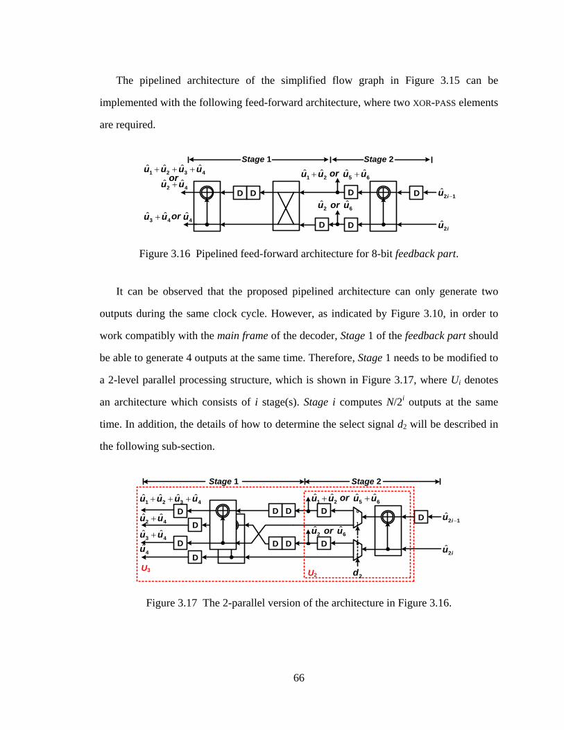
66
The pipelined architecture of the simplified flow graph in Figure 3.15 can be
implemented with the following feed-forward architecture, where two XOR-PASS elements
are required.
D
DD
DD ˆ−iu2 1
ˆ iu2
D
orˆ ˆu u+1 2 ˆ ˆu u+5 6
ˆ ˆ u or u2 6
ˆ ˆu u+2 4
ˆ ˆ ˆ ˆu u u u+ + +1 2 3 4or
ˆ ˆu u+3 4 u4or
Stage 1 Stage 2
Figure 3.16 Pipelined feed-forward architecture for 8-bit feedback part.
It can be observed that the proposed pipelined architecture can only generate two
outputs during the same clock cycle. However, as indicated by Figure 3.10, in order to
work compatibly with the main frame of the decoder, Stage 1 of the feedback part should
be able to generate 4 outputs at the same time. Therefore, Stage 1 needs to be modified to
a 2-level parallel processing structure, which is shown in Figure 3.17, where Ui denotes
an architecture which consists of i stage(s). Stage i computes N/2i outputs at the same
time. In addition, the details of how to determine the select signal d2 will be described in
the following sub-section.
0
1
0
1
D
D
D
D
D
D
DD
DD
ˆ ˆ ˆ ˆu u u u+ + +1 2 3 4
ˆ ˆ+u u2 4
ˆ ˆ+u u3 4
u4
orˆ ˆu u+1 2 ˆ ˆu u+5 6
ˆ ˆ u or u2 6
U2U3 d2
D ˆ−iu2 1
ˆ iu2
Stage 1 Stage 2
Figure 3.17 The 2-parallel version of the architecture in Figure 3.16.

67
In general, for an N-bit length decoder, since the data structures of the feedback part
are defined recursively for powers of 2, the general parallel pipelined architecture can be
constructed with the recurrence relationship. The recursion for the general case is shown
explicitly in Figure 3.18.
……
D
D D …
2n-1-2
D
D D …
2n-1-2
D
D D …
2n-1-2
Un-1
ˆ−iu2 1
ˆ iu2
Un
…
……
…
0
1
0
1
0
1
0
1
0
1
0
1
D
D
D
D
D
D
……
Stage (log2N-n+1)
Figure 3.18 Recursive construction of Un based on Un-1.
Here module Un can be constructed based on module Un-1 and (n-1) extra XOR-PASS
elements. It can be observed that in order to cooperate with the main frame perfectly, the
delay elements have been rearranged to equip each stage with output registers. For Un
with n0 = log2N, the de-multiplexers are not required.
Selecting Signals for De-/Multiplexers 3.4.5
Another important issue we need to address clearly is at which time instance the de-
/multiplexers need to be switched. As shown in Figure 3.10, the select signals of the
multiplexers and de-multiplexers in Stage i are denoted as mi and di (1≤i<log2N),

68
respectively. The switching schedule for mi can be obtained according to Table 3.3. The
corresponding clock cycle index (c) is determined with the following equation:
,j jj
c b w i= +∑ (3-17)
where bj, wj, and i represent the binary digit, weight, and stage index, respectively. The
values of mi are assigned to be alternately “0” and “1”. For example, for Stage 1, m1 is set
to 0 in Clock cycle 1, where 31 0 2 1 1.- += ×( )
Although it can be observed in Figure 3.10 that m3 is actually not required in the
design, the given switch time for m3 is still helpful to determine the clock cycle when
each decoded bit is output. As indicted by Table 3.1, the decoded bits with odd indices
are output in Clock cycles 3, 6, 10, and 13. Those with even indices are output in Clock
cycles 4, 7, 11, and 14.
Table 3.3 Calculation of switching time for mn.
Weight Stage index Clock cycle mn 23-1 22-1 21-1 Stage 1 (n = 1)
0 –– –– 1 1 0 1 –– –– 1 8 1
Stage 2 (n = 2) 0 0 –– 2 2 0 0 1 –– 2 5 1 1 0 –– 2 9 0 1 1 –– 2 12 1
Stage 3 (n = 3) 0 0 0 3 3 0 0 0 1 3 4 1 0 1 0 3 6 0 0 1 1 3 7 1 1 0 0 3 10 0 1 0 1 3 11 1 1 1 0 3 13 0 1 1 1 3 14 1

69
In order to determine the switching time for de-multiplexers’ control signal di, we re-
visit Figure 3.10. Two properties are observed as follows:
1. Signal di needs to be set as 0 one clock cycle before signal mi is set as 1;
2. Signal di needs to be set as 1 in the same clock cycle when any dj (i<j) is set as 0.
Using these properties along with Table 3.3, the switch details for mi and di signals
shown in Figure 3.10 are listed in Table 3.4 below.
Table 3.4 Select signals for 8-bit decoder example.
Clock cycle m1 m2 d2 1 0 –– –– 2 –– 0 –– 3 –– –– –– 4 –– –– 0 5 –– 1 –– 6 –– –– –– 7 –– –– 1 8 1 –– –– 9 –– 0 –– 10 –– –– –– 11 –– –– 0 12 –– 1 –– 13 –– –– –– 14 –– ––
Pre-Computation Look-Ahead Sequential Decoder 3.5
Since the transformed DFG of the conventional SC decoder has been derived in Section
3.3, it provides us a more fundamental way to explain the pre-computation look-ahead
approach. In this section, a novel pre-computation look-ahead sequential SC polar
decoder architecture is presented based on the DFG analysis. Comparison has shown that
this architecture can achieve 50% decoding latency with similar hardware consumption.

70
Architecture of the Revised Type I PE 3.5.1
According to the pre-computation look-ahead scheme, the Type I PE in the pre-
computation look-ahead decoder is in charge of pre-computing two possible outputs in
parallel. Therefore, the new Type I PE is called the revised Type I PE here.
In the revised Type I PE, we need to incorporate both capabilities of adding or
subtracting operands together and finish them simultaneously. As shown in Figure 3.19,
the straightforward parallel implementation of the Type I PE can be employed here. It
can be observed that in the straightforward way, two identical copies of the architecture
in Figure 3.11 are employed.
…1-bit full
adder
YW-1
SW-1
CW
1-bit full adder CW-1
XW-1
DW-1
BW BW-1 1-bit full adder
Y2
S2
C3
1-bit full adder
X2
D2
B3 1-bit full adder
Y1
S1
C2
1-bit full adder
X1
D1
B2 1-bit full adder
Y0
S0
C1
1-bit half adder
X0
D0
B1 1
…
…
…
Figure 3.19 The W-bit parallel adder-subtractor architecture.
However, simple duplication results in penalty of doubling both area and power
consumption. For a W-bit parallel adder-subtractor, totally 2W-1 1-bit full adder and one
1-bit half adder are required. In order to implement the revised Type I PE more
effectively, the complexity-reduced architecture of the parallel adder-subtractor is
proposed here. Rather than implementing the revised Type I PE with two’s complement
approach, the original carry-borrow idea is employed here. Suppose X and Y are the two
operands, and Zin is the carried-in or borrowed-from bit. For the 1-bit full adder, the two
output bits of summation and carry-out are represented by S and Cout, respectively. In

71
similar way, the difference and borrow-out bits produced by the 1-bit full subtractor are
denoted with D and Bout. Therefore, the truth table for the 1-bit full adder and subtractor
is given as follows.
Table 3.5 Truth table of both full adder and subtractor.
Inputs Outputs
Adder Subtractor X Y Zin S Cout D Bout 0 0 0 0 0 0 0 0 0 1 1 0 1 1 0 1 0 1 0 1 1 0 1 1 0 1 0 1 1 0 0 1 0 1 0 1 0 1 0 1 0 0 1 1 0 0 1 0 0 1 1 1 1 1 1 1
From Table 3.5, we can draw the corresponding Karnaugh map for all outputs. Then
the logic equations are derived as follows:
;( ) .
in
out in
S X Y ZC X Y X Y Z= ⊕ ⊕
= ⋅ + ⊕ ⋅ (3-18)
;
.in
out in
D X Y Z
B X Y X Y Z
= ⊕ ⊕
= ⋅ + ⊕ ⋅ (3-19)
According to the equations, it can be noticed that S and D are actually the same. With
the help of Boolean logic, we know that X Y⋅ is an intermediate term of X Y⊕
operation. Similarly, ( ) inX Y Z⊕ ⋅ can be treated as a byproduct of the term inX Y Z⊕ ⊕
as well. These observations enable us to employ the gate-level sub-block sharing scheme
to implement the required parallel adder-subtractor. This scheme not only implements the
parallel processing but also helps us to reduce the hardware consumption. The gate-level

72
structures of the proposed 1-bit parallel full and half adder-subtractor are depicted in
Figure 3.20 (a) and (b), respectively.
Bin
X
Y
Cin
D
Bout
S
Cout
(a) 1-bit parallel full adder-subtractor.
X
YS D
Bout
Cout
(b) 1-bit parallel half adder-subtractor.
Figure 3.20 Proposed 1-bit parallel adder-subtractor architectures.
For the sake of easy estimation and comparison, the hardware consumption of the
proposed architectures is converted in the form of equivalent XOR gate number.
According to Figure 3.20, the complexities of 1-bit parallel full and half adder-subtractor
equal to 4 XOR gates and 1 XOR gate, respectively. Compared with the straightforward
implementation methods, the total hardware savings of the proposed approaches are 43%
and 50%, respectively.

73
Y0
S0
C1
1-bit half adder-
subtractor
X0
D0
B1
Y1
S1
C2
1-bit full adder-
subtractor
X1
D1
B2
YW-1
SW-1
CW
1-bit full adder-
subtractor
XW-1
DW-1
BW
CW-1
BW-1…
…
…
Type I PE
YX
DS
Figure 3.21 The revised Type I PE architecture.
Illustrated in Figure 3.21, the revised Type I PE is composed of W-1 1-bit full adder-
subtractor and a 1-bit half adder-subtractor. With the proposed design method, it requires
57% hardware of the conventional one in Figure 3.19 while achieves exactly the same
function.
Architecture of the Merged PE 3.5.2
TtoS
TtoSsgnsgn
mag
mag
StoTMerged PE
( ) ( ),
( ) ( ), ,
( )
ˆ( , ); ˆ ˆ( , ), ;ˆ ˆ ˆ ˆ( , ); ( , ) .ˆ( , );
− −+ −
− − −−
−
=⊕ =,
2 2 2 -1 2 22 2 1 1 1 1 2 11 22 2 2 2 2 2 -1 2 2
2 2 1 1 1 3 1 1 2 12 -1 2 2
1 1 1
0input : output :input : output : 1output :
i N i i N iN N e N ii N i i i N iN o e N i
i N iN
y u y u uy u u y u uy u
1input
2input1output
q
q
q
qqq
Type I PE
Bn
0
1
S
D
01
10
StoT2outputq
StoT3outputq
Figure 3.22 Proposed structure of the merged PE.
Since in the pre-computation look-ahead approach, the function of the Type II PE
stays unchanged, the corresponding hardware architecture is the same as the one
illustrated in Figure 3.12. According to Figure 3.12, a comparator is required by the Type
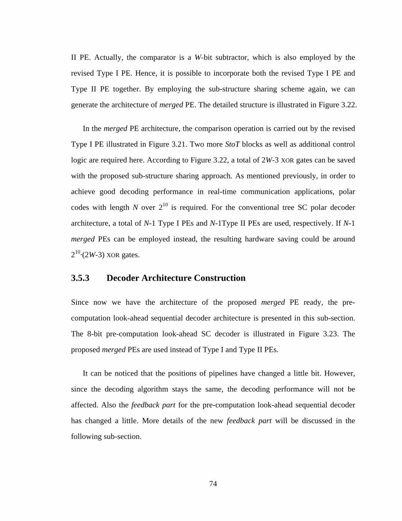
74
II PE. Actually, the comparator is a W-bit subtractor, which is also employed by the
revised Type I PE. Hence, it is possible to incorporate both the revised Type I PE and
Type II PE together. By employing the sub-structure sharing scheme again, we can
generate the architecture of merged PE. The detailed structure is illustrated in Figure 3.22.
In the merged PE architecture, the comparison operation is carried out by the revised
Type I PE illustrated in Figure 3.21. Two more StoT blocks as well as additional control
logic are required here. According to Figure 3.22, a total of 2W-3 XOR gates can be saved
with the proposed sub-structure sharing approach. As mentioned previously, in order to
achieve good decoding performance in real-time communication applications, polar
codes with length N over 210 is required. For the conventional tree SC polar decoder
architecture, a total of N-1 Type I PEs and N-1Type II PEs are used, respectively. If N-1
merged PEs can be employed instead, the resulting hardware saving could be around
210∙(2W-3) XOR gates.
Decoder Architecture Construction 3.5.3
Since now we have the architecture of the proposed merged PE ready, the pre-
computation look-ahead sequential decoder architecture is presented in this sub-section.
The 8-bit pre-computation look-ahead SC decoder is illustrated in Figure 3.23. The
proposed merged PEs are used instead of Type I and Type II PEs.
It can be noticed that the positions of pipelines have changed a little bit. However,
since the decoding algorithm stays the same, the decoding performance will not be
affected. Also the feedback part for the pre-computation look-ahead sequential decoder
has changed a little. More details of the new feedback part will be discussed in the
following sub-section.

75
0
1
ˆ−iu2 1
Stage 3Stage 2Stage 1
ˆ iu2
: Merged PE
0
1
0
1
ˆ ˆ u or u2 6
orˆ ˆu u+1 2
ˆ ˆu u+5 6
u4
0
1
0
1
0
1
0
1
I1
I2
O1
O2
O3
I1
I2
O1
O2
O3
ˆ ˆ ˆ ˆu u u u+ + +1 2 3 4
ˆ ˆu u+3 4
ˆ ˆu u+2 4
( ) ( )L y11 1
( ) ( )L y11 2
( ) ( )L y11 3
( ) ( )L y11 4
( ) ( )L y11 5
( ) ( )L y11 6
( ) ( )L y11 7
( ) ( )L y11 8
I1
I2
O1
O2
O3
I1
I2
O1
O2
O3
I1
I2
O1
O2
O3
I1
I2
O1
O2
O3
0
1
0
1
ˆ ˆ ˆ ˆu u u u+ + +1 2 3 4
ˆ ˆ+u u2 4
ˆ ˆ+u u3 4
u4
orˆ ˆu u+1 2 ˆ ˆu u+5 6
ˆ ˆ u or u2 6
DDD
DDD
DDD
DDD D
DD
DDD
D
D
D
D
D
D
0
1
0
1
0
1
0
1
0
1
0
1
m1
m2
d2
I1
I2
O1
O2
O3
I1
I2
O1
O2
O3
Figure 3.23 8-bit pre-computation look-ahead polar decoder architecture.
Architecture of the Revised Feedback Part 3.5.4
Compared with the one shown in Figure 3.10, only half of the delay elements are
employed by the feedback loop in accordance with the halved decoding latency. This is
simply because the entire decoding latency of the proposed pre-computation look-ahead
sequential decoder has been halved.
The revised feedback part for the N-bit length pre-computation look-ahead decoder is
shown as follows (Figure 3.24). Compared to the one in Figure 3.18, the only difference
is the number of delay elements prior to each XOR-PASS element is (2n-2-2) rather than (2n-
1-2).

76
……
D
D D …
2n-2-2
D
D D …
2n-2-2
D
D D …
2n-2-2
Un-1
ˆ−iu2 1
ˆ iu2
Un
…
……
…
0
1
0
1
0
1
0
1
0
1
0
1
D
D
D
D
D
D
……
Stage (log2N-n+1)
Figure 3.24 Revised recursive construction of Un based on Un-1.
Note that slight modification of control signal mi is required. The revised calculation
of the switching time is shown in Table 3.6.
Table 3.6 Revised calculation of switching time for mn.
Weight Stage index Clock cycle mn 22-1 21-1 Stage 1 (n = 1)
0 –– 1 2 0 1 –– 1 5 1
Stage 2 (n = 2) 0 0 2 3 0 0 1 2 4 1 1 0 2 6 0 1 1 2 7 1
It can be observed that since the total decoding latency has been halved, the switching
time for the signal mi should be revised according to Eq. (3-20). This is because the
position of delay elements in the main frame is now before the multiplexers rather than
after them.
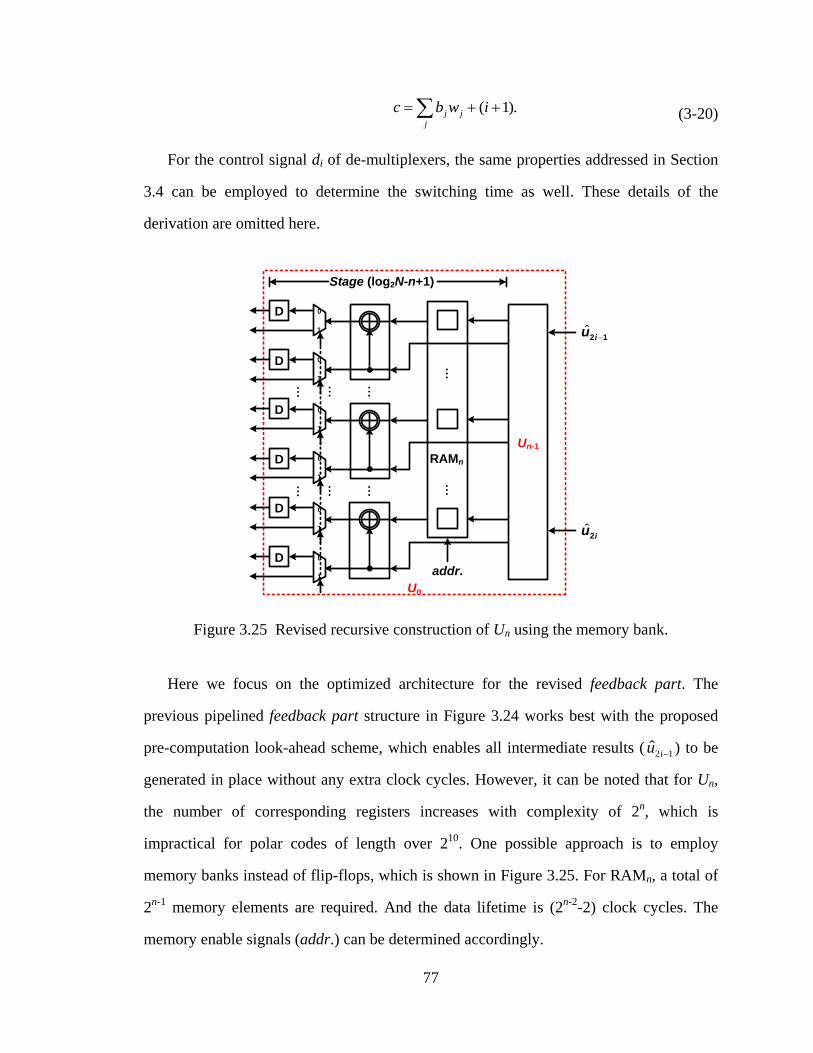
77
( 1).j jj
c b w i= + +∑ (3-20)
For the control signal di of de-multiplexers, the same properties addressed in Section
3.4 can be employed to determine the switching time as well. These details of the
derivation are omitted here.
……
Un-1
ˆ−iu2 1
ˆ iu2
Un
……
0
1
0
1
0
1
0
1
0
1
0
1
D
D
D
D
D
D
……
Stage (log2N-n+1)
…
RAMn
addr.
…
Figure 3.25 Revised recursive construction of Un using the memory bank.
Here we focus on the optimized architecture for the revised feedback part. The
previous pipelined feedback part structure in Figure 3.24 works best with the proposed
pre-computation look-ahead scheme, which enables all intermediate results ( 2 1ˆ iu − ) to be
generated in place without any extra clock cycles. However, it can be noted that for Un,
the number of corresponding registers increases with complexity of 2n, which is
impractical for polar codes of length over 210. One possible approach is to employ
memory banks instead of flip-flops, which is shown in Figure 3.25. For RAMn, a total of
2n-1 memory elements are required. And the data lifetime is (2n-2-2) clock cycles. The
memory enable signals (addr.) can be determined accordingly.

78
Comparison of Latency and Hardware 3.6
In this section, we compare the decoding latency and the hardware consumption for the
proposed pre-computation look-ahead sequential SC polar decoder along with the state-
of-the-art references [28, 92]. Table 3.7 lists the comparison results of those designs in
terms of hardware consumption, decoding latency, and data throughput. The design in the
1st column is the implementation of the proposed pre-computation look-ahead sequential
decoding schedule in Section 3.5. The design in the 2nd column is the straightforward SC
polar decoder design proposed in [28]. The one in the 3rd column is the tree design
presented in [92].
The most significant point is that, due to the pre-computation look-ahead decoding
scheme, all the proposed architectures require only half the latency of their counterparts.
This advantage makes the proposed decoders more attractive for practical
implementations, which always demand code length N higher than 210. This means that
we can always achieve twice higher data throughput with the proposed pre-computation
approach.

79
Table 3.7 Comparison for different polar decoder architectures.
Different designs Proposed pre-computation look-ahead sequential design Straightforward design [28] Tree design [92]
Hardware consumption # of merged PEs N-1 (Nlog2N)/2 N-1
1 PE XOR 9W 11W-3 REG 0 1 MUX 6W 5W
# of fbk parts N-1 ––
1 fbk part
XOR N/2-1 –– RAM N/2-2 –– MUX N/2-2 ––
# of other REGs W(3N-4) W(Nlog2N)/2 W(N-1) # of other MUXs W(2N-3) 0 0
Total XOR ~17WN ~(16W-3)(Nlog2N)/2 ~(16W-3)N REG ~3WN ~(W+1)N(Nlog2N)/2 ~(W+1)N
Decoding schedule Latency N-1 2(N-1) 2(N-1)
Throughput 2 1 1

80
The second design point that should be underlined is the proposed feedback part. The
design of the feedback part is inspired by the real FFT processor proposed in [87]. It
outputs all control bits (for the pre-computation look-ahead decoders) required by the
multiplexers on the fly. Its architecture can be generated in a nice and easy recursive
manner. Therefore, with the help of the feedback part, no additional clock cycles are
needed for computation of 2 1ˆ iu − , which preserves the advantage of short latency. To the
best of our knowledge, this is the first detailed design of the feedback module with such
features.
Usually, in order to fairly compare the decoder designs, both throughput and
hardware consumption need to be taken into account. In Table 3.7, a detailed hardware
architecture comparison for the proposed decoder design has been presented. Meanwhile,
since no information could be found in reference [92] for the “ ˆsu computation block”,
which is the counterpart of the proposed feedback part, only the hardware consumption
for the main frame is compared. Despite larger number of registers, which inherently
result from the pre-computation look-ahead scheme, the proposed design requires much
less hardware compared with the straightforward design proposed in [28]. Even
compared with the state-of-the-art design listed in the 3rd column, the proposed design
consumes similar hardware area (in terms of number of XOR gates). More specifically, the
proposed pre-computation look-ahead sequential design needs 6.25% more hardware than
the one presented in [28]. However, considering the latency reduction it can achieve, this
small overhead hardware is acceptable. Here, without loss of generality, all data
throughputs are represented in a normalized format.

81
Conclusion 3.7
In this chapter, based on thorough investigation of the DFG for the conventional tree SC
polar decoder, a novel pre-computation look-ahead sequential decoder architecture for
polar codes, which can halve the decoding latency required by conventional approaches,
is proposed.
For efficient hardware implementation, a merged PE is presented by using the sub-
structure sharing technique. Its control signal 2 1ˆ iu − can be generated with a real FFT-like
diagram. This unique feature is directly applied to develop an efficient architecture for
the feedback part, which works best with the low-latency polar decoder architectures.
Compared with its conventional counterparts, aside from the feedback part, the proposed
design shows comparable hardware utilization with 50% decoding latency. The next
work will be directed towards designing architectures for even higher throughput
communication applications.
Equation Chapter 4 Section 1

82
Chapter 4
High-Throughput Interleaved SC Polar
Decoders
This chapter presents SC polar decoder architectures which are suitable for high-
throughput applications. A brief introduction is given in Section 4.1. Section 4.2 presents
a TC 3-interleaved SC polar decoder example. A general discussion on the properties of
TC interleaved SC decoder architectures [58] is conducted in Section 4.3. Section 4.4
introduces a new design approach using folding technique. Based on the folding
technique, the RC interleaved SC decoder architectures [59] are proposed in Section 4.5.
Comparison with other works is conducted in Section 4.6. Section 4.7 concludes this
chapter.
Introduction 4.1
In Chapter 3, the pre-computation look-ahead approach helps us to reduce the decoding
latency of polar decoders by 50%. However, the proposed pre-computation look-ahead
serial decoder still needs to be improved for real-time communication applications. It can
be noticed that for the proposed pre-computation look-ahead sequential SC decoder

83
architecture, although the hardware utilization of each active stage is 100%, other stages
still remain idle at the same time. For the proposed 8-bit pre-computation look-ahead SC
polar decoder example, a total of 7 clock cycles are required before the next code-word
can be processed.
Generally, for an N-bit pre-computation look-ahead SC polar decoder, each code-
word needs (N-1) clock cycles to be properly decoded with the given pre-computation
look-ahead approach. During the entire process no new code-word could be input to the
decoder. Therefore, even as high as half of the decoding latency has been reduced by the
pre-computation look-ahead SC polar decoder, the data throughput and hardware
utilization remain low for large values of N. To this end, the pre-computation TC
interleaved polar decoder architectures are proposed in this chapter. For the TC
interleaved approach, the decoding latency stays the same, and more PEs can be added.
Another way to improve the decoding throughput is to introduce the RC interleaved
processing. The RC interleaved approach always employs the same number of PEs while
optimizing the decoding schedule. Compared with the pre-computation polar decoder
proposed in [36], the RC 2-interleaved decoder proposed here can achieve 200%
throughput with only 50% hardware consumption. Even if the number of processing
elements (PEs) required is the same as [94], our design achieves up to four times
throughput. Detailed architecture including the control logic is given as well. The general
RC L-interleaved polar decoder is also proposed and discussed with respects to both
hardware and latency.
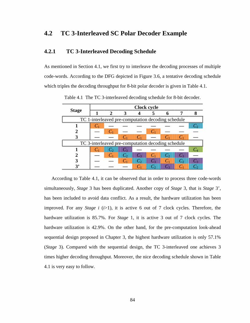
84
TC 3-Interleaved SC Polar Decoder Example 4.2
TC 3-Interleaved Decoding Schedule 4.2.1
As mentioned in Section 4.1, we first try to interleave the decoding processes of multiple
code-words. According to the DFG depicted in Figure 3.6, a tentative decoding schedule
which triples the decoding throughput for 8-bit polar decoder is given in Table 4.1.
Table 4.1 The TC 3-interleaved decoding schedule for 8-bit decoder.
Stage Clock cycle 1 2 3 4 5 6 7 8
TC 1-interleaved pre-computation decoding schedule 1 C1 –– –– –– –– –– –– C2 2 –– C1 –– –– C1 –– –– –– 3 –– –– C1 C1 –– C1 C1 ––
TC 3-interleaved pre-computation decoding schedule 1 C1 C2 C3 –– –– –– –– C4 2 –– C1 C2 C3 C1 C2 C3 –– 3 –– –– C1 C2 C3 C1 C2 C3 3’ –– –– –– C1 C2 C3 C1 C2
According to Table 4.1, it can be observed that in order to process three code-words
simultaneously, Stage 3 has been duplicated. Another copy of Stage 3, that is Stage 3’,
has been included to avoid data conflict. As a result, the hardware utilization has been
improved. For any Stage i (i>1), it is active 6 out of 7 clock cycles. Therefore, the
hardware utilization is 85.7%. For Stage 1, it is active 3 out of 7 clock cycles. The
hardware utilization is 42.9%. On the other hand, for the pre-computation look-ahead
sequential design proposed in Chapter 3, the highest hardware utilization is only 57.1%
(Stage 3). Compared with the sequential design, the TC 3-interleaved one achieves 3
times higher decoding throughput. Moreover, the nice decoding schedule shown in Table
4.1 is very easy to follow.

85
TC 3-Interleaved SC Decoder Architecture 4.2.2
Based on the pre-computation look-ahead sequential SC decoder we have got previously,
the TC 3-interleaved SC polar decoder architecture can be obtained as illustrated in
Figure 4.1. It is worth noting that Stage 3 and 3’, which are activated in serial, are
generated by using the unfolding transformation technique [104] with factor of 2. Since
the consecutive 3 input code-words are independent, a total of 3 identical copies of the
feedback part are required as a result. { }i means the closure clock cycle index associated
with the corresponding point is 7n+i, where n≥0.
D
0
1
( ) ( )L y11 1
( ) ( )L y11 2
( ) ( )L y11 3
( ) ( )L y11 4
( ) ( )L y11 5
( ) ( )L y11 6
( ) ( )L y11 7
( ) ( )L y11 8
Stage 2Stage 1
0
1
0
1
0
1
0
1
0
1
I1
I2
O1
O2
O3
ˆ ˆ u or u2 6
orˆ ˆu u+1 2
ˆ ˆu u+5 6
ˆ ˆ ˆ ˆu u u u+ + +1 2 3 4
ˆ ˆu u+3 4
ˆ ˆu u+2 4
u4
DDD
DDD
D
DDD
DDD
D
DDD
DDD
D
DDD
DDD
D
DDD
DDD
D
DDD
DDD
D
Stage 3 and 3'
0
1
I1
I2
O1
O2
O3
0
1
I1
I2
O1
O2
O3
0
1
U1U2
d1
0
1
0
1
D
D
U1U2
d1
0
1
0
1
U2U3
0
1
12
3{4, 7}
{3, 6}{4, 7}
{4, 7}
{3, 6}{4, 7}
0
1
0
1
0
1
0
1
m1
ˆ−iu2 1
ˆ iu2
ˆ−iu2 1
ˆ iu2
d1
{4}{6}{5}
D
D
{3, 6}{5, 1}
{4, 0}
{5, 1}
{5, 1}
{3, 6}{5, 1}
{5, 1}
{3, 6}
I1
I2
O1
O2
O3
I1
I2
O1
O2
O3
I1
I2
O1
O2
O3
I1
I2
O1
O2
O3
I1
I2
O1
O2
O3
D
DD
DD
DD
DD
Figure 4.1 The 8-bit TC 3-interleaved SC polar decoder.

86
Properties of TC Interleaved SC Decoder Architectures 4.3
Although higher decoding throughput has been achieved by the proposed TC 3-
interleaved decoder example, the iteration bound of the SC decoder has not been
achieved yet. According to the DFG analysis of the pre-computation look-ahead time
chart presented in Chapter 3, for an N-bit SC polar decoder, the maximum value of
concurrent inputs is (N-1). Therefore, how to systematically construct the TC (N-1)-
interleaved SC polar decoder while guaranteeing the sequential decoding process still
needs to be addressed.
Moreover, if only TC M-interleaved processing is required, where 1≤M≤N-1, what is
the relationship between the concurrent number M and the hardware consumption? Here
the concurrent number represents the maximum number of code-words the decoder can
process at the same time. The design approach proposed in Section 4.2 can be treated as
an empirical design method, which is somewhat case-specific. Can we derive a formal
design methodology which only costs the minimal design efforts while meets all the
design requirements. All these issues are well addressed with the following four
properties.
Property 1 For an N-bit pre-computation look-ahead polar decoder, the highest
concurrent number M is (N-1).
Proof According to the recursive construction of the pre-computation look-ahead DFG,
the decoding latency equals
2 2log 1 log
0
2 12 12 1
N Ni
iN
−
=
−= = −
−∑ (4-1)
clock cycles. During the entire decoding process for a single code-word, Stage 1 is only
activated during one clock cycle. Therefore, in the remaining (N-2) clock cycles, Stage 1

87
is available for other possible input code-words. The maximum number of other input
code-words is (N-2). Therefore, the highest possible concurrent number is (N-1).∎
Property 2 For a given N-bit pre-computation look-ahead polar decoder, its TC (2i-1)-
interleaved version can be constructed based on its TC (2i-1-1)-interleaved version. The
method is: A. find out the (2i-1-1) stages with the most significant stage indices of the TC
(2i-1-1)-interleaved decoder; B. duplicate each of those (2i-1-1) stages.
Proof It can be noticed that
12 1 2 (2 1) 1,i i−− = × − + (4-2)
which is in the same form as the pre-computation look-ahead decoder. In order to achieve
maximum hardware utilization of the entire decoder (or certain specific stages), the
number of PEs in each relative decoding stage should stay the same. Since the DFG is
constructed in the time domain, we only need to apply the same approach in the “stage
domain”, which leads to Property 2.∎
A simple example is employed here for a better explanation. For instance, now we
would like to construct the TC 3-interleaved version of 8-bit pre-computation look-ahead
polar decoder based on the TC 1-interleaved version (or the sequential one proposed in
Chapter 3). According to Property 2, we have
2
1
3 2 11 2 1.2-
= -= -
(4-3)
Therefore, we can determine that i = 2. We only need to include another copy of Stage 3
(that is Stage 3’) to get the decoder architecture illustrated in Figure 4.1.

88
Table 4.2 The TC 1-, 3-, and 7-interleaved decoding schedule for 8-bit decoder.
Stage Clock cycle 1 2 3 4 5 6 7 8 9 10 11 12 13 14
TC 1-interleaved pre-computation decoding schedule 1 C1 –– –– –– –– –– –– C2 –– –– –– –– –– –– 2 –– C1 –– –– C1 –– –– –– C2 –– –– C2 –– –– 3 –– –– C1 C1 –– C1 C1 –– –– C2 C2 –– C2 C2
TC 3-interleaved pre-computation decoding schedule 1 C1 C2 C3 –– –– –– –– C4 C5 C6 –– –– –– –– 2 –– C1 C2 C3 C1 C2 C3 –– C4 C5 C6 C4 C5 C6 3 –– –– C1 C2 C3 C1 C2 C3 –– C4 C5 C6 C4 C5 3’ –– –– –– C1 C2 C3 C1 C2 C3 –– C4 C5 C6 C4
TC 7-interleaved pre-computation decoding schedule 1 C1 C2 C3 C4 C5 C6 C7 ⋯ 2 –– C1 C2 C3 C4 C5 C6 C7 ⋯ 3 –– –– C1 C2 C3 C4 C5 C6 C7 ⋯ 3’ –– –– –– C1 C2 C3 C4 C5 C6 C7 ⋯ 2’ –– –– –– –– C1 C2 C3 C4 C5 C6 C7 ⋯ 3’’ –– –– –– –– –– C1 C2 C3 C4 C5 C6 C7 ⋯ 3’’’ –– –– –– –– –– –– C1 C2 C3 C4 C5 C6 C7 ⋯

89
Moreover, its TC 7-interleaved version, which can achieve 100% hardware utilization
in each decoding stage, can be constructed based on the TC 3-interleaved one accordingly
as shown in Table 4.2. The construction steps are shown as follows. According to
Property 2, since
3
3 1
7 2 13 2 1,-
= -= -
(4-4)
We have i = 3. For the TC 3-interleaved version decoder, the 3 stages with the most
significant indices are Stage 2, 3, and 3’. Therefore, the architecture of the TC 7-
interleaved pre-computation look-ahead SC polar decoder can be derived based on the
TC 3-interleaved one by duplicating Stage 2, 3, and 3’. According to Table 4.2, it can be
seen that the proposed TC 7-interleaved decoder can handle all 7 inputs perfectly and
achieve 100% utilization rate during any Decoding iteration i (i>1). Also the iteration
bound is achieved as a result.
Since all the interleaving factors mentioned now can be represented in the form of (2i-
1), what if when we are required to implement a TC M-interleaved decoder with M which
could not be written in the form of (2i-1)? This problem can be addressed by Property 3
as follows.
Property 3 For any M which satisfies 2i-1-1<M≤2i-1, the TC M-interleaved polar
decoder requires the same amount of hardware as the TC (2i-1)-interleaved version. A
100% hardware utilization can be achieved if and only if M = N-1.
Proof The proof of Property 2 can be used to prove this. According to Property 2, it
can be noted that (2i-1) is the maximum number of code-words the TC (2i-1)-interleaved
version decoder can handle. This gives the proof.∎

90
Table 4.3 The TC 3-, 5-, and 7-interleaved decoding schedule for 8-bit decoder.
Stage Clock cycle 1 2 3 4 5 6 7 8 9 10 11 12 13 14
TC 3-interleaved pre-computation decoding schedule 1 C1 C2 C3 –– –– –– –– C4 C5 C6 –– –– –– –– 2 –– C1 C2 C3 C1 C2 C3 –– C4 C5 C6 C4 C5 C6 3 –– –– C1 C2 C3 C1 C2 C3 –– C4 C5 C6 C4 C5 3’ –– –– –– C1 C2 C3 C1 C2 C3 –– C4 C5 C6 C4
TC 5-interleaved pre-computation decoding schedule 1 C1 C2 C3 C4 C5 –– –– C6 C7 C8 C9 C10 –– –– 2 –– C1 C2 C3 C4 C5 –– –– C6 C7 C8 C9 C10 –– 3 –– –– C1 C2 C3 C4 C5 –– –– C6 C7 C8 C9 C10 3’ –– –– –– C1 C2 C3 C4 C5 –– –– C6 C7 C8 C9 2’ –– –– –– –– C1 C2 C3 C4 C5 –– –– C6 C7 C8 3’’ –– –– –– –– –– C1 C2 C3 C4 C5 –– –– C6 C7 3’’’ –– –– –– –– –– –– C1 C2 C3 C4 C5 –– –– C6
TC 7-interleaved pre-computation decoding schedule 1 C1 C2 C3 C4 C5 C6 C7 ⋯ 2 –– C1 C2 C3 C4 C5 C6 C7 ⋯ 3 –– –– C1 C2 C3 C4 C5 C6 C7 ⋯ 3’ –– –– –– C1 C2 C3 C4 C5 C6 C7 ⋯ 2’ –– –– –– –– C1 C2 C3 C4 C5 C6 C7 ⋯ 3’’ –– –– –– –– –– C1 C2 C3 C4 C5 C6 C7 ⋯ 3’’’ –– –– –– –– –– –– C1 C2 C3 C4 C5 C6 C7 ⋯

91
A simple example in Table 4.3 clearly shows that the TC 5-interleaved version
consumes the same number of PEs as the TC 7-interleaved decoder does.
Now, we are ready to derive the relationship between the concurrent number M and
the hardware consumption.
Property 4 For any M which satisfies 2i-1-1<M≤2i-1, the hardware consumption stays
the same. The total number of merged PEs employed by the M-concurrent polar decoder
is N+2i-1∙(i-2), where N is the code length of the polar codes.
Proof According to Property 1, the number of merged PEs can be calculated as follows:
2log 11
1
1 1
1
2 2 ( 1)
( 2 ) 2 ( 1)2 ( 2).
Nj i
j i
i i
i
i
N iN i
−−
= −
− −
−
+ ⋅ −
= − + ⋅ −
= + ⋅ −
∑
(4-5)
For example, according to the calculations given by Property 4, the TC 1-, 3-, 5-, and 7-
interleaved versions of 8-bit pre-computation look-ahead polar decoder are supposed to
have 7, 8, 12, and 12 merged PEs, respectively. By checking the details shown in both
Table 4.2 and Table 4.3, those results can be easily verified.
With the four properties proposed in this chapter, we now have a systematic
methodology to design TC interleaved versions of pre-computation look-ahead SC polar
decoders for various application requirements.
The Construction Approach with Folding Technique 4.4
The folding transformation provides a systematic technique for designing control circuits
where multiple algorithm operations are time-multiplexed to a single function unit [37].

92
The folding transformation technique can help us derive a formal procedure for designing
a family of architectures for a specific DSP algorithm [105, 106]. In this section, we will
see, with the help of the folding transformation technique, existing hardware architectures
can be implemented systematically.
Preliminaries of Folding Transformation Technique 4.4.1
To implement the folding transformation upon the DFG, a folding set is required first.
Each folding set is an ordered set of n operations executed by the same PE [37]. The
operation in the i-th position in the folding set is executed by the PE during the i-th time
instance. For example, according to the folding set 1 2 3{ , , , }A A A Aφ= , we have n = 4.
Operations 1A , 2A , and 3A will be carried out by PE A at clock cycle 4l+1, 4l+2, and 4l,
respectively. Since the 3rd operation within the folding set is null, no operation will be
executed by PE A during clock cycle 4l+3.
Aside from the folding set, another key factor we should be aware of is the folding
equation. The folding equation is employed to calculate the number of delay elements
associated with a specific directed edge in the DFG. The general form of the n-folding
equation can be written as follows:
( ) ( )eF UD U V nw e P v u→ = − + − (4-6)
Here, e is the w(e) weighted directed edge connecting PE U and PE V. ( )eFD U V→ is
the number of folding delay elements associated with edge e. PE U is PU-stage pipelined.
u and v are the folding set indices of PE U and PE V, respectively. About the derivation
of the folding equation, please refer to Chapter 6 of [105] for more details.
93
Previous Decoders with Folding Transformation Technique 4.4.2
In this sub-section, we will derive the previous SC polar decoder architectures based on
the folding transformation technique.
Tree Architecture of the SC Decoder
First, let us re-visit the DFG illustrated in Figure 3.5. The SC decoder architecture
proposed in [28] can be treated as the original version which has not been folded yet.
Then, the tree architecture of the SC polar decoder in [92] can be constructed with the
following folding sets:
1 1 1 1
2 2 2
3 3
4 4
{ , , , , , , , , , , , , , }, { , , , , , , , , , , , , , },
{ , , , , , , , , , , , , , }, { , , , , , ,
{ , , , , , , , , , , , , , },
{ , , , , , , , , , , , , , };
f f
f f
f
f
A A B BA A BA A
A A
φ φ φ φ φ φ φ φ φ φ φ φ φ φ φ φ φ φ φ φ φ φ φ φ φ φ
φ φ φ φ φ φ φ φ φ φ φ φ φ φ φ φ φ φ φ φ
φ φ φ φ φ φ φ φ φ φ φ φ φ
φ φ φ φ φ φ φ φ φ φ φ φ φ
= =
= =
= =
2
3 3
4 4
1 1 3 1 1
2 2 4
, , , , , , , },
{ , , , , , , , , , , , , , },
{ , , , , , , , , , , , , , }.
{ , , , , , , , , , , , , , }; { , , , , , , , , , , ,
{ , , , , , , , , , , , , , }.
f
f
f f
f
BB B
B B
C C C D D D
C C C
φ φ φ φ φ φ
φ φ φ φ φ φ φ φ φ φ φ φ φ
φ φ φ φ φ φ φ φ φ φ φ φ φ
φ φ φ φ φ φ φ φ φ φ φ φ φ φ φ φ φ φ φ φ φ φ
φ φ φ φ φ φ φ φ φ φ φ φ
= =
= =
=
3
2 2 4
1 1 2 3 4 1 1 2 3 4
, , };
{ , , , , , , , , , , , , , }.{ , , , , , , , , , , , , , }. { , , , , , , , , , , , , , }.
f
f f
D D DE E E E E F F F F F
φ φ
φ φ φ φ φ φ φ φ φ φ φ φφ φ φ φ φ φ φ φ φ φ φ φ φ φ φ φ φ φ φ φ
== =
(4-7)
Here, the superscript “f” means “folding”. Assume neither Type I PE nor Type II PE
has any pipeline stages and 14n = . We can write down the folding equation in Eq. (4-6)
for each of the 28 edges in the DFG (Figure 3.5). The equations are:
1,2 1 1 1,2
3,4 2 1,2 2
1,2 1 2 2
1 1 2 1,2,3,4
1,2 3 3 3,4
3,4 4 3,4 4
3,4 3 4 4
3
( ) 1, ( ) 1,( ) 1, ( ) 1,( ) 1, ( ) 1,( ) 1, ( ) 1;( ) 1, ( ) 1,( ) 1, ( ) 1,( ) 1, ( ) 1.(
F F
F F
F F
F F
F F
F F
F F
F
D A C D F DD A C D D ED C E D E FD E F D F BD B C D F DD B C D D ED C E D E FD E
→ = → =→ = → =→ = → =→ = → =
→ = → =→ = → =→ = → =→ 3 ) 1,F =
(4-8)
94
For example, 1,2 1( ) 1FD A C→ = means that the outputs of both 1fA and 2
fA will be
hold for 1 clock cycle before they are output to node 1fC .Therefore, the tree architecture
proposed by Figure 4 of [92] can be derived accordingly.
Pre-Computation Look-Ahead Sequential Decoder Architecture
Now we derive the pre-computation look-ahead sequential decoder architecture with the
folding transformation technique. Consider the following folding sets:
1 1
2 2
3 3
4 4
1 1 3
2 2 4
1 1
( ) {( ) , , , , , , },
( ) {( ) , , , , , , },
( ) {( ) , , , , , , },
( ) {( ) , , , , , , }.
( ) { , ( ) , , , ( ) , , };
( ) { , ( ) , , , ( ) , , }.( ) { , , ( ) ,
f
f
f
f
f
f
f
AB ABAB ABAB ABAB AB
CD CD CDCD CD CD
EF EF
φ φ φ φ φ φ
φ φ φ φ φ φ
φ φ φ φ φ φ
φ φ φ φ φ φ
φ φ φ φ φ
φ φ φ φ φφ φ
=
=
= =
=
== 2 3 4( ) , , ( ) , ( ) }.EF EF EFφ
(4-9)
Again, suppose neither Type I nor Type II PEs has any pipeline stages and 7n = . The
folding equations are as follows:
1,2 1 1 1,2
3,4 2 1,2 2
1,2 1 2 2
1 1 2 1,2,3,4
1,2 3 3 3,4
3,4 4 3,4 4
3,4 3 4 4
( ) 1, ( ) 1,( ) 1, ( ) 2,( ) 1, ( ) 0,( ) 0, ( ) 3;( ) 4, ( ) 1,( ) 4, ( ) 2,( ) 1, ( ) 0.(
F F
F F
F F
F F
F F
F F
F F
F
D A C D F DD A C D D ED C E D E FD E F D F BD B C D F DD B C D D ED C E D E FD
→ = → = −→ = → =→ = → =→ = → = −
→ = → = −→ = → =→ = → =
3 3 ) 0,E F→ =
(4-10)
For example, 1,2 3( ) 4FD B C→ = means that the outputs of both 1fB and 2
fB will be
hold for 4 clock cycles before they are output to node 1fC . 2 1,2,3,4( ) 3FD F B→ = −
indicates that the outputs of nodes 1,2,3,4fB will be hold for 3 clock cycles until the output
of 1fF arrives. The pre-computation decoder can therefore be realized in Figure 3.10.

95
Pre-Computation TC Interleaved Decoder Architecture
For the efficient TC interleaved decoder architectures in Section 4.2 and Section 4.3, they
can also be derived by changing the folding sets. We know that the TC interleaved pre-
computation look-ahead decoder architectures are categorized into a big family. Without
loss of generality, here we only show the construction details for the TC 3-interleaved
decoder architecture. Other TC interleaved versions can be derived in a similar fashion.
Consider the new folding sets listed as follows, where the superscripts “1”, “2”, and
“3” mean the PE is dealing with Codeword 1, Codeword 2, and, Codeword 3,
respectively.
(1) (2) (3)1 1 1 1
(1) (2) (3)2 2 2 2
(1) (2) (3)3 3 3 3
(1) (2) (3)4 4 4 4
(11 1
( ) {( ) , ( ) , ( ) , , , , },
( ) {( ) , ( ) , ( ) , , , , },
( ) {( ) , ( ) , ( ) , , , , },
( ) {( ) , ( ) , ( ) , , , , }.
( ) { , ( )
f
f
f
f
f
AB AB AB ABAB AB AB ABAB AB AB ABAB AB AB AB
CD CD
φ φ φ φ
φ φ φ φ
φ φ φ φ
φ φ φ φ
φ
=
=
= =
= ) (2) (3) (1) (2) (3)1 1 3 3 3
(1) (2) (3) (1) (2) (3)2 2 2 2 4 4 4
(3) (1) (2) (3) (1) (2)1 3 1 1 1 3 3
(2)1 4
, ( ) , ( ) , ( ) , ( ) , ( ) };
( ) { , ( ) , ( ) , ( ) , ( ) , ( ) , ( ) }.
( ) {( ) , , ( ) , ( ) , ( ) , ( ) , ( ) },
( ) {( ) ,
f
f
f
CD CD CD CD CDCD CD CD CD CD CD CD
EF EF EF EF EF EF EFEF EF
φ
φ
=
=
= (3) (1) (2) (3) (1)4 2 2 2 4( ) , , ( ) , ( ) , ( ) , ( ) }.EF EF EF EF EFφ
(4-11)
Here we can also derive the hardware utilization from the folding sets. Take the
following folding set as an example:
(3) (1) (2) (3) (1) (2)1 3 1 1 1 3 3( ) {( ) , , ( ) , ( ) , ( ) , ( ) , ( ) }.fEF EF EF EF EF EF EFφ= (4-12)
It can be observed from the folding set that only 1 out of 7 clock cycle is occupied by the
null operation. Therefore, the hardware utilization of Stage 3’ is 85.7%, which matches
the previous analysis in Section 4.2. The utilization of other stages can be derived in the
same manner.
96
The corresponding folding equations are given as follows. With these folding
equations, the TC 3-interleaved pre-computation look-ahead decoder can be constructed:
(1,2,3) (1,2,3) (1,2,3) (1,2,3)1,2 1 1 1,2(1,2,3) (1,2,3) (1,2,3) (1,2,3)3,4 2 1,2 2(1,2,3) (1,2,3) (1,2,3) (1,2,3)1,2 1 2 2
(1,2,3) (1,2,3)1 1 2 1
( ) 1, ( ) 1,( ) 1, ( ) 1,( ) 1, ( ) 1,
( ) 1, (
F F
F F
F F
F F
D A C D F DD A C D D ED C E D E F
D E F D F B
→ = → =→ = → =→ = → =→ = → (1,2,3)
,2,3,4
(1,2,3) (1,2,3) (1,2,3) (1,2,3)1,2 3 3 3,4(1,2,3) (1,2,3) (1,2,3) (1,2,3)3,4 4 3,4 4(1,2,3) (1,2,3) (1,2,3) (1,2,3)3,4 3 4 4(1,2,3) (13 3
) 1;
( ) 1, ( ) 1,( ) 1, ( ) 1,( ) 1, ( ) 1.(
F F
F F
F F
F
D B C D F DD B C D D ED C E D E FD E F
=
→ = → =→ = → =→ = → =→ ,2,3) ) 1,=
(4-13)
The RC Interleaved Pre-Computation Decoders 4.5
In Section 4.2 and Section 4.3, the TC interleaved decoder architectures are proposed.
However, in order to achieve higher decoder throughput, the TC interleaved decoders
required higher hardware consumption. Therefore, the decoder architecture with higher
data rate and lower hardware cost is appreciated. To this end, the RC interleaved pre-
computation look-ahead decoder architecture is present based on the folding
transformation technique. In order to save the hardware consumption, for N-bit RC
interleaved decoders, the number of merged PEs employed is always N/2. Also, in order
to increase the data rate, we try to process multiple code-words in an interleaved manner.
The Original Design Employing N/2 Merged PEs 4.5.1
Now we construct the folding sets for the original 8-bit SC polar decoder which only
employs 4 merged PEs:

97
1 1 1 1 2 3 3 4
2 2 2 4
3 3
4 4
( ) {( ) , ( ) , ( ) , ( ) , ( ) , ( ) , ( ) },
( ) {( ) , ( ) , , , ( ) , , },
( ) {( ) , , , , , , },
( ) {( ) , , , , , , }.
f
f
f
f
AB AB CD EF EF CD EF EFAB AB CD CDAB ABAB AB
φ φ φ φ
φ φ φ φ φ φ
φ φ φ φ φ φ
=
=
= =
(4-14)
The decoding schedule of the original decoder design employing 4 merged PEs is
listed in Table 4.4 as follows:
Table 4.4 Number of active merged PEs for the original decoder.
PE Clock cycle
1 2 3 4 5 6 7 1 2 –– –– –– –– 3 –– –– –– –– –– –– 4 –– –– –– –– –– ––
The RC 2-Interleaved Decoders 4.5.2
According to the decoding schedule of the original decoder design, it is observed that we
can use the same number of merged PEs to carry out the decoding of two code-words at
the same time. Now we construct the folding sets for the 8-bit RC 2-interleaved SC polar
decoder as follows:
(1) (2) (1) (1) (1) (1) (1) (1)1 1 1 1 1 2 3 3 4
(1) (2) (1) (1)2 2 2 2 4
(1) (2) (2) (2)3 3 3 1 3
4 4
( ) {( ) , ( ) , ( ) , ( ) , ( ) , ( ) , ( ) , ( ) },
( ) {( ) , ( ) , ( ) , , , ( ) , , },
( ) {( ) , ( ) , ( ) , , , ( ) , , },
( ) {( )
f
f
f
f
AB AB AB CD EF EF CD EF EFAB AB AB CD CDAB AB AB CD CDAB AB
φ φ φ φ
φ φ φ φ
=
=
=
= (1) (2) (2) (2) (2) (2) (2) (2)4 2 1 2 4 3 4, ( ) , ( ) , ( ) , ( ) , ( ) , ( ) , ( ) }.AB CD EF EF CD EF EF
(4-15)
Again, it is assumed that there are no pipelines within any PE. The folding factor n is
set to 8. By applying Eq. (4-6), we have the following folding equations for the new
folding sets:

98
(1) (1) (1) (1)1,2 1 1 1,2(1) (1) (1) (1)3,4 2 1,2 2(1) (1) (1) (1)1,2 1 2 2(1) (1) (1) (1)1 1 2 1,2,3,4
(1) (1) (1) (1)1,2 3 3 3,4
( ) 2, ( ) 1,( ) 2, ( ) 2,( ) 1, ( ) 0,( ) 0, ( ) 4;
( ) 5, ( )
F F
F F
F F
F F
F F
D A C D F DD A C D D ED C E D E FD E F D F B
D B C D F D
→ = → = −→ = → =→ = → =→ = → = −
→ = → =(1) (1) (1) (1)3,4 4 3,4 4(1) (1) (1) (1)3,4 3 4 4(1) (1)3 3
(2) (2) (2) (2)1,2 1 1 1,2(2) (2) (2) (2)3,4 2 1,2 2(2) (2)1,2 1
1,( ) 5, ( ) 2,( ) 1, ( ) 0.( ) 0,
( ) 1, ( ) 1,( ) 1, ( ) 2,( ) 1,
F F
F F
F
F F
F F
F
D B C D D ED C E D E FD E F
D A C D F DD A C D D ED C E
−→ = → =→ = → =→ =
→ = → = −→ = → =→ = (2) (2)
2 2(2) (2) (2) (2)1 1 2 1,2,3,4
(2) (2) (2) (2)1,2 3 3 3,4(2) (2) (2) (2)3,4 4 3,4 4(2) (2) (2) (2)3,4 3 4 4(2) (2)3 3
( ) 0,( ) 0, ( ) 3;
( ) 4, ( ) 1,( ) 4, ( ) 2,( ) 1, ( ) 0.( ) 0,
F
F F
F F
F F
F F
F
D E FD E F D F B
D B C D F DD B C D D ED C E D E FD E F
→ =→ = → = −
→ = → = −→ = → =→ = → =→ =
(4-16)
According to the new folding sets in Eq. (4-15), the RC 2-interleaved SC polar
decoder architecture employing four merged PEs is illustrated in Figure 4.2. Since the
routing for the RC 2-interleaved decoder architecture is a little bit complicated, different
colors are employed for better identification. The control signals of the decoder
architecture can be determined according to the folding sets. The switching schedule of
all the control signals is listed in Table 4.5 as follows:
Table 4.5 Control signals for the RC 2-interleaved decoder.
Signal Clock cycle 1 2 3 4 5 6 7 8
m1 –– –– 0 0 1 1 0 1 m2 –– –– 0 –– –– 1 –– –– d1 –– –– –– 0 1 –– –– ––
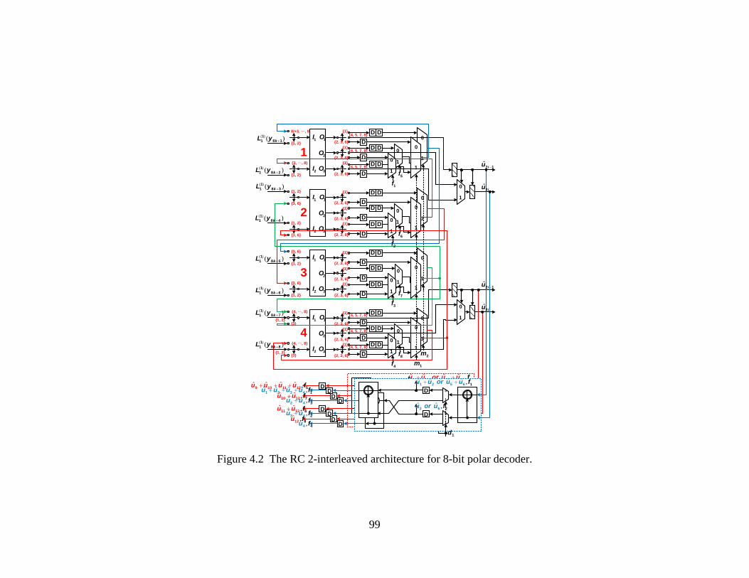
99
I1
I2
O1
O2
O3
DD D
DD D
DD D
0
1
0
1
0
1
I1
I2
O1
O2
O3
DD D
DD D
DD D
0
1
0
1
0
10
1
I1
I2
O1
O2
O3
DD D
DD D
DD D
0
1
0
1
0
10
1
I1
I2
O1
O2
O3
DD D
DD D
DD D
0
1
0
1
0
10
1
0
1
{1}
{1}
{1}
{2, 3, 6}
{2, 3, 6}
{2, 3, 6}
{1}
{1}
{1}
{2, 3, 6}
{2, 3, 6}
{2, 3, 6}
{1}
{1}
{1}
{2, 3, 6}
{2, 3, 6}
{2, 3, 6}
{1}
{1}
{1}
{2, 3, 6}
{2, 3, 6}
{2, 3, 6}
{4, 5, 7, 8}
{4, 5, 7, 8}
{4, 5, 7, 8}
{4, 5, 7, 8}
{4, 5, 7, 8}
{4, 5, 7, 8}
0
1
{1, 2}
{3, …, 8}
{1, 2}
{1, 2}
{1, 2}
{1, 2}
{1, 2}
{1, 2}
{1, 2}
{3, 6}
{3, 6}
{3, 6}
{3, 6}
{4, …, 8}
{4, …, 8}
{3}
{3}
8l+3, …, 8
orˆ ˆu u+1 2 ˆ ˆu u+5 6
ˆ ˆ u or u2 6
0
1
0
1
D
D
D
D
D
D
ˆ ˆ ,ˆ ˆ+ + +u u u u f9 10 11 12 5
ˆ ˆ ,+u u f10 12 7
ˆ ˆ ,+u u f11 12 6
ˆ ,u f12 8
ˆ ˆ ˆ ˆ ,+ +u u or u u f9 10 13 14 3
ˆ ˆ ,u or u f10 14 4
0
1
0
1
D
D
D
D
D
D
ˆ ˆ ,ˆ ˆ+ + +u u u u f1 2 3 4 1
ˆ ˆ ,+u u f2 4 3
ˆ ˆ ,+u u f3 4 2
ˆ ,u f4 4
ˆ ˆ ˆ ˆ ,+ +u u or u fu1 2 5 6 1
ˆ ˆ ,u or u f2 6 2
( ) ( )+kL y11 8 3
( ) ( )+kL y11 8 4
( ) ( )+kL y11 8 5
( ) ( )+kL y11 8 6
( ) ( )+kL y11 8 7
( ) ( )+kL y11 8 8
( ) ( )+kL y11 8 1
( ) ( )+kL y11 8 2
0
1
ˆ−iu2 1
ˆ iu2
ˆ−iu2 1
ˆ iu2
d1
f1
f2
f3
f4
f5
f6
f7
f8 m2
m1
1
2
3
4
Figure 4.2 The RC 2-interleaved architecture for 8-bit polar decoder.

100
For easier understanding of the decoding schedule of the proposed RC 2-interleaved
polar decoder, the four merged PEs are marked with red labels. The number of active
PE(s) in each clock cycle is shown in Table 4.6.
Table 4.6 Number of active merged PEs for RC 2-interleaved decoder.
PE Clock cycle
1 2 3 4 5 6 7 8 1 2 –– –– –– –– 3 –– –– –– –– 4
∎: dealing with Codeword 1; ∎: dealing with Codeword 2.
Indicated by the cardinality of the folding sets, in order to complete the decoding
process of both code-words, a total of 8 clock cycles are required. Compared with the
conventional pre-computation look-ahead decoding process, an additional clock cycle is
required. In general, the N-bit RC 2-interleaved SC decoder’s decoding latency equals N
clock cycles. For real-time communication applications, the code length N is considerable
large, the one clock cycle penalty is negligible. At the same time, its advantages are
obvious: the decoding throughput has been doubled while the hardware cost is only 50%
as before.
In general, to construct an L-interleaved N-bit polar decoder architecture, the brute-
force way is to simply duplicate the proposed RC 2-interleaved decoder 2L times.
Therefore, a total of 22N L⋅ merged PEs and N clock cycles are required. In this case,
the decoding latency will remain as N clock cycles.
However, in our design situation, since the resources are constrained, we have to stick
with 2N merged PEs. To avoid too large decoding latency, further optimization is required.
According to the DFG analysis in Section 3.3, for the pre-computation look-ahead
sequential decoder in Figure 3.10, Stage i is associated with 12i− clock cycles’ latency.

101
Compare the proposed RC 2-interleaved decoder architecture in Figure 4.2 with the one
illustrated in Figure 3.10. If we are trying to process L code-words in an interleaved
manner using the same architecture in Figure 4.2, the resulting latency associated with
Stage i in Figure 3.10 is 11
22 ii L
−− ⋅ clock cycles. Therefore, the entire decoding latency
for this RC L-interleaved decoder is:
2
1
log1
21
2 .i
Ni L
iT −
−
=
= ⋅ ∑ (4-17)
Let us see some examples. First, let 2L = and 8,N = we have the decoding latency
for the RC 2-interleaved 8-bit polar decoder architecture is
2
1
1
0 1 2
log 81 2
(8,2) 21
31 2
21
0 1 22 2 22 2 2
2
2
2 2 2
2 2 48,
i
i
i
i
i
i
T −
−
−
=
−
=
= ⋅
= ⋅
= ⋅ + ⋅ + ⋅ = + +=
∑
∑ (4-18)
which matches the result shown in Table 4.6.
Then, we try to calculate the decoding latency for the RC 3-interleaved example. Set
3L = and 8,N = we have the decoding latency is
2
1
1
0 1 2
log 81 3
(8,3) 21
31 3
21
0 1 23 3 32 2 2
2
2
2 2 2
3 4 411.
i
i
i
i
i
i
T −
−
−
=
−
=
= ⋅
= ⋅
= ⋅ + ⋅ + ⋅ = + +=
∑
∑ s (4-19)
On the other hand, the decoding schedule of the RC 3-interleaved decoder can be
described by Table 4.7 as follows:

102
Table 4.7 Number of active merged PEs for RC 3-interleaved decoder.
PE Clock cycle
1 2 3 4 5 6 7 8 9 10 11 1 2 3 –– –– –– –– –– –– 4 –– ––
∎: dealing with Codeword 1; ∎: dealing with Codeword 2; ∎: dealing with Codeword 3.
Again, we have two results match with each other. However, in real applications the
RC 2-interleaved pre-computation look-ahead decoder is the most favorable one. Because
it can achieve good balance of both decoding throughput and hardware cost.
Comparison with Other Works 4.6
In this section, we conduct a comparison with the state-of-the-art designs. Both the pre-
computation look-ahead TC interleaved decoder design and the RC interleaved decoder
design proposed in this chapter are included in the comparison. For the TC M-interleaved
polar decoder, it is assumed that 2i-1-1<M≤2i-1. For the RC interleaved polar decoder
architecture, the 2-interleaved version is compared here. The previous decoders which
have already been mentioned in Table 3.7 are not compared here. The other designs
included in Table 4.8 are the conventional overlapped decoder in [92], the line decoder in
[94], and the pre-computation look-ahead sequential decoder proposed in Section 3.5. All
the design details are listed in Table 4.8. The same assumptions on the hardware
conversion and throughput estimation, which are used in Table 3.7, are also adopted here.
Also, since the merged PE architecture we proposed in Chapter 3 consumes similar
hardware compared with the conventional one, no more gate count details are provided
here.

103
Table 4.8 Comparison between the two proposed works and others.
Different designs Number of merged PEs Number of feedback parts Latency Throughput Pre-computation TC interleaved design N+2i-1∙(i-2) M N-1 2M
Pre-computation RC 2-interleaved design N/2 2 N 4
Pre-computation look-ahead sequential design N-1 1 N-1 2
Overlapped design [92] ~N+M(log2M/2)/2 –– 2(N-1) 1
Line design [94] N/2 –– 2(N-1) 1
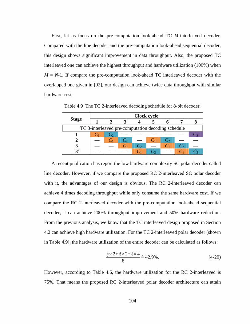
104
First, let us focus on the pre-computation look-ahead TC M-interleaved decoder.
Compared with the line decoder and the pre-computation look-ahead sequential decoder,
this design shows significant improvement in data throughput. Also, the proposed TC
interleaved one can achieve the highest throughput and hardware utilization (100%) when
M = N-1. If compare the pre-computation look-ahead TC interleaved decoder with the
overlapped one given in [92], our design can achieve twice data throughput with similar
hardware cost.
Table 4.9 The TC 2-interleaved decoding schedule for 8-bit decoder.
Stage Clock cycle 1 2 3 4 5 6 7 8
TC 3-interleaved pre-computation decoding schedule 1 C1 C2 –– –– –– –– –– C3 2 –– C1 C2 –– C1 C2 –– –– 3 –– –– C1 C2 –– C1 C2 –– 3’ –– –– –– C1 C2 –– C1 C2
A recent publication has report the low hardware-complexity SC polar decoder called
line decoder. However, if we compare the proposed RC 2-interleaved SC polar decoder
with it, the advantages of our design is obvious. The RC 2-interleaved decoder can
achieve 4 times decoding throughput while only consume the same hardware cost. If we
compare the RC 2-interleaved decoder with the pre-computation look-ahead sequential
decoder, it can achieve 200% throughput improvement and 50% hardware reduction.
From the previous analysis, we know that the TC interleaved design proposed in Section
4.2 can achieve high hardware utilization. For the TC 2-interleaved polar decoder (shown
in Table 4.9), the hardware utilization of the entire decoder can be calculated as follows:
4 4 27 7 72 2 4 42.9%.
8× × ×+ +
(4-20)
However, according to Table 4.6, the hardware utilization for the RC 2-interleaved is
75%. That means the proposed RC 2-interleaved polar decoder architecture can attain
105
even higher utilization than its TC interleaved counterpart. Low latency, high throughput,
and high utilization make the RC 2-interleaved SC polar decoder very attractive for real-
time applications.
Conclusion 4.7
In this chapter, two kinds of interleaved SC polar decoder architectures are proposed.
Compared with the pre-computation look-ahead sequential decoder, they can achieve
even higher throughput. With the properties introduced, the pre-computation look-ahead
TC interleaved decoder family can be constructed in a systematic manner. With the
overlapping scheme, the hardware utilization can be as high as 100%. Also, the RC
interleaved SC decoder family is presented. A formal design methodology is introduced
as well. Comparison results have shown that the RC 2-interleaved pre-computation look-
ahead decoder can achieve 4 times decoding throughput compared with the state-of-the-
art design in [92].
Equation Chapter 5 Section 1

106
Chapter 5
Design of Simplified SC Polar Decoders
This chapter presents the latency analysis and the architecture design of simplified SC
(SSC) polar decoders [61]. The remainder of this chapter is organized as follows. A brief
introduction is given in Section 5.1. A review of the SSC decoding algorithm is provided
in Section 5.2. In Section 5.3, a systematic way to calculate the latency for the SSC
decoder is proposed. An SSC polar decoder architecture is presented in Section 5.4.
Using the pre-computation technique, the latency-reduced SSC decoder architecture is
presented in Section 5.5. Comparison results with state-of-the-art works are presented in
Section 5.6. Section 5.7 concludes this chapter.
Introduction 5.1
According to Chapter 3 and Chapter 4, we can see that the decoder architecture design is
an active area of research. In real-time applications, to guarantee better performance over
turbo codes or LDPC codes, polar codes’ code length N needs to be greater 210. For the
SC decoding algorithm [28], the long code length leads to a significant increase in
decoding latency. To widely employ polar codes in real-time applications, the design of
107
low-latency decoders is greatly needed. In previous chapters, we have provided several
design methodologies to address this problem. However, the few existing SC decoders
fail to completely satisfy this requirement. According previous analysis, the decoding
latency for conventional SC decoders in [28, 92, 94] is 2(N-1). In Chapter 3 and Chapter
4, though the pre-computation technique is used, their decoding latency remains (N).
Significant research has been directed towards code constructions and decoding
algorithms for polar codes. However, how to construct efficient SC polar decoders with
even shorter latency is still a problem.
To this end, [60] introduced a modified decoding scheme called the simplified SC
(SSC) decoding algorithm is introduced. First, the SSC algorithm removes all the
redundant computations required by the rate-zero constituent codes. Second, by
simplifying local decoders for rate-one constituent codes, the SSC algorithm can further
reduce the decoding latency. However, how to efficiently determine the decoding latency
for one specific polar code has not been addressed yet. Hardware implementation for the
SSC decoding algorithm has not been proposed either. Another important issue, which
we should be aware of is, in some cases the decoding latencies for the SSC decoder are
still longer than those in [36, 58, 59].
In this paper, first we propose a systematic way to calculate the decoding latency for
the SSC algorithm. With this method, we can calculate the decoding latency for any
given polar code easily. Then a formal design flow for the SSC decoder architecture is
developed. Finally, in order to always achieve a lower decoding latency than those in [36,
58, 59], a novel pre-computation SSC decoder architecture is also proposed.

108
Review of the SSC Algorithm 5.2
Tree Representation of the SC Decoding Algorithm 5.2.1
Previously, the FFT-like butterfly trellis shown in Figure 3.3 is employed to denote the
SC decoding process. [60] has shown that the binary tree can also be employed to provide
another representation of the SC decoding algorithm. Again, the 8-bit polar decoder is
used as the running example to give a clear explanation.
0 1 2 3 4 5 6 7
v
pv
vl vr
βv
αv
αlv
βlv β
rv
αrv
Stage 1
Stage 2
Stage 3
Figure 5.1 Tree representation of the 8-bit SC polar decoder.
As illustrated in Figure 5.1, like the previous trellis representation, this binary tree can
be partitioned into three stages. In general, except of the last stage, each stage is
composed of one level of nodes of the binary tree. The last stage is composed of the two
bottom levels of the binary tree.
Every node within the binary tree representation is associated with some message
vectors. For any Node v, ( )v vα β , ( )l lv vα β , and ( )
r rv vα β are the message vectors passing
between node v and its parent pv, left child vl, and right child vr, respectively. If, Node v is
located in the last stage, we have sgn( )v vβ α= , and this vβ is the decoding result of the
corresponding code bit. With those new notations, the SC decoding algorithm can be re-
descripted by the following equations:

109
Clock cycle 1
0 1 2 3 4 5 6 7
v
pv
vl vr
βv
αv
αlv
βlv β
rv
αrv
Stage 1
Stage 2
Stage 3
(a)
Clock cycle 2
0 1 2 3 4 5 6 7
v
pv
vl vr
βv
αv
αlv
βlv β
rv
αrv
Stage 1
Stage 2
Stage 3
(b)
Clock cycle 3
0 1 2 3 4 5 6 7
v
pv
vl vr
βv
αv
αlv
βlv β
rv
αrv
Stage 1
Stage 2
Stage 3
ˆ:output u1
(c)
Clock cycle 4
0 1 2 3 4 5 6 7
v
pv
vl vr
βv
αv
αlv
βlv β
rv
αrv
Stage 1
Stage 2
Stage 3
ˆ:output u2
(d)
Clock cycle 5
0 1 2 3 4 5 6 7
v
pv
vl vr
βv
αv
αlv
βlv β
rv
αrv
Stage 1
Stage 2
Stage 3
(e)
Clock cycle 6
0 1 2 3 4 5 6 7
v
pv
vl vr
βv
αv
αlv
βlv β
rv
αrv
Stage 1
Stage 2
Stage 3
ˆ:output u3
(f)
Clock cycle 7
0 1 2 3 4 5 6 7
v
pv
vl vr
βv
αv
αlv
βlv β
rv
αrv
Stage 1
Stage 2
Stage 3
ˆ:output u4
(g)
Clock cycle 8
0 1 2 3 4 5 6 7
v
pv
vl vr
βv
αv
αlv
βlv β
rv
αrv
Stage 1
Stage 2
Stage 3
(h)
Clock cycle 9
0 1 2 3 4 5 6 7
v
pv
vl vr
βv
αv
αlv
βlv β
rv
αrv
Stage 1
Stage 2
Stage 3
(i)

110
Clock cycle 10
0 1 2 3 4 5 6 7
v
pv
vl vr
βv
αv
αlv
βlv β
rv
αrv
Stage 1
Stage 2
Stage 3
ˆ:output u5
(j)
Clock cycle 11
0 1 2 3 4 5 6 7
v
pv
vl vr
βv
αv
αlv
βlv β
rv
αrv
Stage 1
Stage 2
Stage 3
ˆ:output u6
(k)
Clock cycle 12
0 1 2 3 4 5 6 7
v
pv
vl vr
βv
αv
αlv
βlv β
rv
αrv
Stage 1
Stage 2
Stage 3
(l)
Clock cycle 13
0 1 2 3 4 5 6 7
v
pv
vl vr
βv
αv
αlv
βlv β
rv
αrv
Stage 1
Stage 2
Stage 3
ˆ:output u7
(m)
Clock cycle 14
0 1 2 3 4 5 6 7
v
pv
vl vr
βv
αv
αlv
βlv β
rv
αrv
Stage 1
Stage 2
Stage 3
ˆ:output u8
(n)
The end.
Figure 5.2 Decoding process of the 8-bit SC decoder with tree representation.
111
The Decoding Scheme for the SC Algorithm
[ ] [2 ] [2 1],
[ ] [2 ](1 2 [ ]) [2 1];
[2 1] [ ],
[2 ] [ ] [ ];
sgn( );
l
r l
r
l r
v v v
v v v v
v v
v v v
v v
from the root nodei i i
i i i i
i i
i i i
v in the last row
α α α
α α β α
β β
β β β
β α
= + = − + +
+ = = ⊕
=
1: begin
2:
3:
4: if 5: 6:
;vβ output 7: endif8: endbegin
For easy understanding of the tree representation, a detailed example is illustrated in
Figure 5.2. The nodes within the red dotted circles stay active during the corresponding
clock cycles.
The SSC Decoding Algorithm 5.2.2
According to the definition of polar codes, the input vector as 1Nu consists of a random part
u and a frozen part cu
. In order to reduce the error rate, when decoding the frozen part, we
simply assign ˆ c cu u=
. Here the values of cu
are known before the decoding process.
Therefore, the tedious computations associated with the frozen part can be removed. The real
decoding task is to generate an estimate u of u [28].
This fact means the node with in the tree representation can be categorized into three
parts: the one nodes which are associated with the random part, the zero nodes which are
associated with the frozen part, and the rest as the mixed nodes. It is assumed that the
polar code illustrated in Figure 5.1 is actually an (8,3,{5,6,7}, (0,0,0,0,0)) code, whose
random part consists of the 5th, 6th, and 7th bits. And all its frozen bits are assigned as “0”.
Its tree representation is given in Figure 5.3 as follows:

112
0 1 2 3 4 5 6 7
v
pv
vl vr
βv
αv
αlv
βlv β
rv
αrv
: zero node
: mixed node : one node
Stage 1
Stage 2
Stage 3
Figure 5.3 The revised tree representation of the 8-bit SC polar decoder.
Since the values of the frozen part are pre-determined, we do not need actually go
through the data flow of the zero nodes. Similarly, the calculations corresponding to the
one nodes can be replaced by the matrix multiplication operations as well. For more
details and the proof, please refer to [60]. In this chapter, we only give the SSC decoding
algorithm as follows:
The Decoding Scheme for the SSC Algorithm { }
[ ] [2 ] [2 1],
[ ] [2 ](1 2 [ ]) [2 1];
[2 1] [ ],
[2 ] [ ] [ ];
{ } ˆ ˆ( [min ], , [max
l
r l
r
l r
v v v
v v v v
v v
v v v
v v
v mixed nodei i i
i i i i
i i
i i i
v zero nodeu u
α α α
α α β α
β β
β β β
∈
= + = − + +
+ = = ⊕
∈
1: if then
2:
3:
4: elseif then5:
2
]) ( [min ], , [max ]);ˆ ˆ( [min ], , [max ]) ;n dv
v v
v v v
u uu u Gβ −
=
=6: else
8: endif
Here v is the set which contains indices of all leaf nodes that are descendants of v. dv
is the depth of v. 2n dvG − denotes the generation matrix of dimension 2 vn d− [60]. Index i can
vary from 0 to 1(2 1)vn d− − − . We can see, the computations of both the zero nodes and the
113
one nodes can be saved as a result. Therefore, the decoding latency and hardware
complexity are reduced.
The Latency Analysis of the SSC Decoder 5.3
Since decoding latency is a key criterion to weigh the polar decoder design, it is
important to be able to estimate the latency accurately for any polar code. However, in
most applications the code length is large and the locations of frozen bits are random. The
calculation for the SSC decoding latency is not trivial. To this end, an efficient approach
to calculate the SSC decoding latency for any polar code is proposed in this section.
A Simple Example 5.3.1
( ) ( )L y11 1
( ) ( )L y11 2
( ) ( )L y11 3
( ) ( )L y11 4
( ) ( )L y11 5
( ) ( )L y11 6
( ) ( )L y11 7
( ) ( )L y11 8
( ) ( )1 88 1L y
( ) ˆ( , )5 8 48 1 1L y u
( ) ˆ( , )3 8 28 1 1L y u
( ) ˆ( , )7 8 68 1 1L y u
( ) ˆ( , )2 88 1 1L y u
( ) ˆ( , )6 8 58 1 1L y u
( ) ˆ( , )4 8 38 1 1L y u
( ) ˆ( , )8 8 78 1 1L y u
Stage 3Stage 2Stage 1
ˆ ˆ ˆ ˆu u u u+ + +1 2 3 4
ˆ ˆu u+3 4
ˆ ˆu u+2 4
u4 u6
u2
ˆ ˆu u+5 6
ˆ ˆu u+1 2
u7
u3
u5
u1
: Processing Element (PE)
A1
B1
A2
B2
A3
B3
A4
B4
C1
C3
D1
D3
C2
C4
D2
D4
E1
E3
E2
E4
F1
F3
F2
F4
Figure 5.4 Conventional SC decoding process.
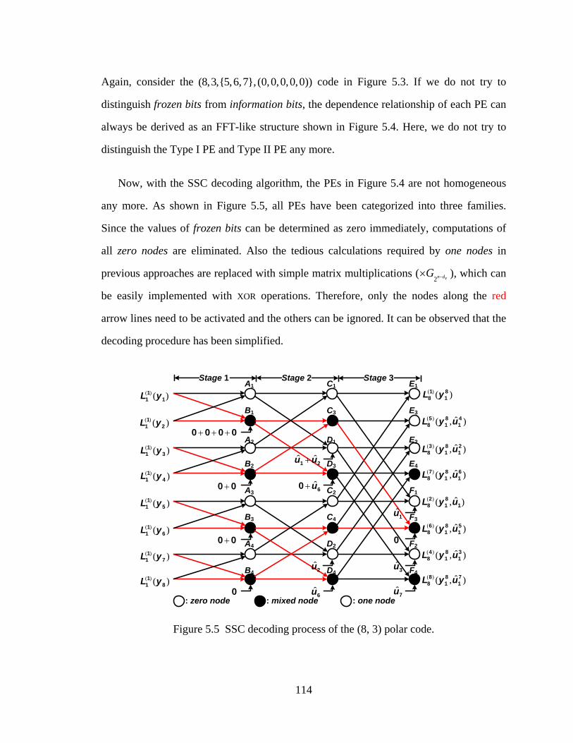
114
Again, consider the (8,3,{5,6,7}, (0,0,0,0,0)) code in Figure 5.3. If we do not try to
distinguish frozen bits from information bits, the dependence relationship of each PE can
always be derived as an FFT-like structure shown in Figure 5.4. Here, we do not try to
distinguish the Type I PE and Type II PE any more.
Now, with the SSC decoding algorithm, the PEs in Figure 5.4 are not homogeneous
any more. As shown in Figure 5.5, all PEs have been categorized into three families.
Since the values of frozen bits can be determined as zero immediately, computations of
all zero nodes are eliminated. Also the tedious calculations required by one nodes in
previous approaches are replaced with simple matrix multiplications (2n dvG −× ), which can
be easily implemented with XOR operations. Therefore, only the nodes along the red
arrow lines need to be activated and the others can be ignored. It can be observed that the
decoding procedure has been simplified.
( ) ( )L y11 1
( ) ( )L y11 2
( ) ( )L y11 3
( ) ( )L y11 4
( ) ( )L y11 5
( ) ( )L y11 6
( ) ( )L y11 7
( ) ( )L y11 8
( ) ( )1 88 1L y
( ) ˆ( , )5 8 48 1 1L y u
( ) ˆ( , )3 8 28 1 1L y u
( ) ˆ( , )7 8 68 1 1L y u
( ) ˆ( , )2 88 1 1L y u
( ) ˆ( , )6 8 58 1 1L y u
( ) ˆ( , )4 8 38 1 1L y u
( ) ˆ( , )8 8 78 1 1L y u
Stage 3Stage 2Stage 1
+ + +0 0 0 0
+0 0
+0 0
0 u6
u2
ˆ+u60
ˆ ˆu u+1 2
u7
u3
0
u1
: one node : zero node : mixed node
A1
B1
A2
B2
A3
B3
A4
B4
C1
C3
D1
D3
C2
C4
D2
D4
E1
E3
E2
E4
F1
F3
F2
F4
Figure 5.5 SSC decoding process of the (8, 3) polar code.
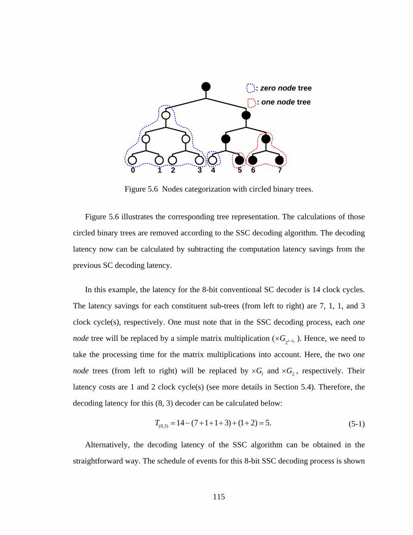
115
0 1 2 3 4 5 6 7
: one node tree
: zero node tree
Figure 5.6 Nodes categorization with circled binary trees.
Figure 5.6 illustrates the corresponding tree representation. The calculations of those
circled binary trees are removed according to the SSC decoding algorithm. The decoding
latency now can be calculated by subtracting the computation latency savings from the
previous SC decoding latency.
In this example, the latency for the 8-bit conventional SC decoder is 14 clock cycles.
The latency savings for each constituent sub-trees (from left to right) are 7, 1, 1, and 3
clock cycle(s), respectively. One must note that in the SSC decoding process, each one
node tree will be replaced by a simple matrix multiplication (2n dvG −× ). Hence, we need to
take the processing time for the matrix multiplications into account. Here, the two one
node trees (from left to right) will be replaced by 1G× and 2G× , respectively. Their
latency costs are 1 and 2 clock cycle(s) (see more details in Section 5.4). Therefore, the
decoding latency for this (8, 3) decoder can be calculated below:
(8,3) 14 (7 1 1 3) (1 2) 5.T = − + + + + + = (5-1)
Alternatively, the decoding latency of the SSC algorithm can be obtained in the
straightforward way. The schedule of events for this 8-bit SSC decoding process is shown
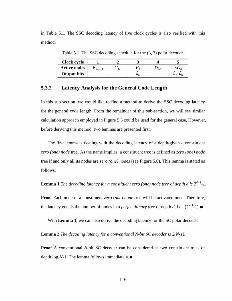
116
in Table 5.1. The SSC decoding latency of five clock cycles is also verified with this
method.
Table 5.1 The SSC decoding schedule for the (8, 3) polar decoder.
Clock cycle 1 2 3 4 5 Active nodes B1,…,4 C3,4 F3 D3,4 ×G2 Output bits –– –– 6u –– 7 8ˆ ˆ,u u
Latency Analysis for the General Code Length 5.3.2
In this sub-section, we would like to find a method to derive the SSC decoding latency
for the general code length. From the remainder of this sub-section, we will see similar
calculation approach employed in Figure 5.6 could be used for the general case. However,
before deriving this method, two lemmas are presented first.
The first lemma is dealing with the decoding latency of a depth-given a constituent
zero (one) node tree. As the name implies, a constituent tree is defined as zero (one) node
tree if and only all its nodes are zero (one) nodes (see Figure 5.6). This lemma is stated as
follows:
Lemma 1 The decoding latency for a constituent zero (one) node tree of depth d is 2d+1-1.
Proof Each node of a constituent zero (one) node tree will be activated once. Therefore,
the latency equals the number of nodes in a perfect binary tree of depth d, i.e., (2d+1-1).∎
With Lemma 1, we can also derive the decoding latency for the SC polar decoder:
Lemma 2 The decoding latency for a conventional N-bit SC decoder is 2(N-1).
Proof A conventional N-bit SC decoder can be considered as two constituent trees of
depth log2N-1. The lemma follows immediately.∎
117
Now, we have both Lemma 1 and Lemma 2 available. By subtracting the clock
savings from the total latency required by the conventional N-bit SC decoders, the SSC
decoding latency for the general code length is obtained as follows.
Theorem 1 The decoding latency T for an N-bit SSC polar decoder can be calculated by:
11
{ } { }2( 1) (2 1) [(2 1) ( 1)],ji dd
ji j
T N d++= − − − − − − +∑ ∑ (5-2)
where { }i and { }j are the sets of zero node trees and one node trees, respectively.
Proof According to Lemma 2, the decoding latency for a conventional N-bit SC decoder
is 2(N-1). Removing a zero node tree of depth d will reduce latency by 12 1d+ − clock
cycles (Lemma 1). Similarly, removing a one node tree will result in the same reduction.
But we need to spend additional clock cycles for the matrix multiplication operation.
With the fully pipelined matrix multiplication block, which is discussed in next section,
d+1 additional clock cycles are required by the “2dG× ” operation. This completes the
proof.∎
Now, we would like to use Theorem 1 for the previous code example. In Figure 5.6,
there are two zero node trees in the binary tree plot, whose depths are 2 and 0,
respectively. There are also two one node trees with depths 1 and 0. According to Eq.
(5-2), the latency for the (8, 3) SSC decoder can be calculated as follows:
3 1 1 2(8,3) 2 (8 1) [(2 1) (2 1)] {[(2 1) (0 1)] [(2 1) (1 1)]}
5,
T = × − − − + − − − − + + − − +
=(5-3)
which matches our previous analysis.
Next we use this method for another code, which is more complicated than the first
code. Consider the code (8,5,{2,3,5,6,7}, (0,0,0)) , its tree representation is illustrated in
Figure 5.7 as follows:
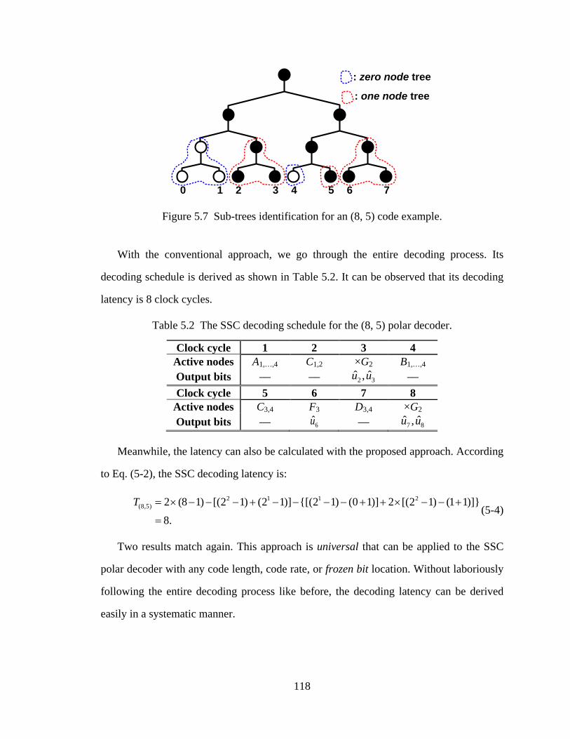
118
0 1 2 3 4 5 6 7
: one node tree
: zero node tree
Figure 5.7 Sub-trees identification for an (8, 5) code example.
With the conventional approach, we go through the entire decoding process. Its
decoding schedule is derived as shown in Table 5.2. It can be observed that its decoding
latency is 8 clock cycles.
Table 5.2 The SSC decoding schedule for the (8, 5) polar decoder.
Clock cycle 1 2 3 4 Active nodes A1,…,4 C1,2 ×G2 B1,…,4 Output bits –– –– 2 3ˆ ˆ,u u –– Clock cycle 5 6 7 8
Active nodes C3,4 F3 D3,4 ×G2 Output bits –– 6u –– 7 8ˆ ˆ,u u
Meanwhile, the latency can also be calculated with the proposed approach. According
to Eq. (5-2), the SSC decoding latency is:
2 1 1 2(8,5) 2 (8 1) [(2 1) (2 1)] {[(2 1) (0 1)] 2 [(2 1) (1 1)]}
8.
T = × − − − + − − − − + + × − − +
=(5-4)
Two results match again. This approach is universal that can be applied to the SSC
polar decoder with any code length, code rate, or frozen bit location. Without laboriously
following the entire decoding process like before, the decoding latency can be derived
easily in a systematic manner.
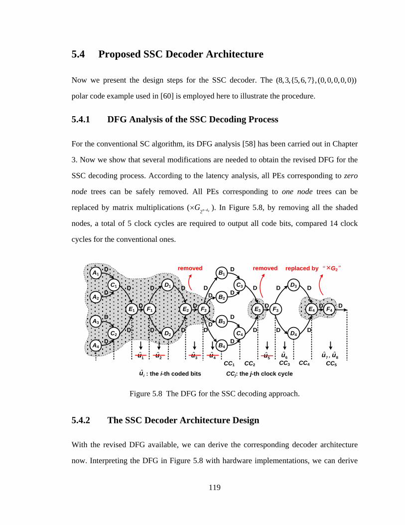
119
Proposed SSC Decoder Architecture 5.4
Now we present the design steps for the SSC decoder. The (8,3,{5,6,7}, (0,0,0,0,0))
polar code example used in [60] is employed here to illustrate the procedure.
DFG Analysis of the SSC Decoding Process 5.4.1
For the conventional SC algorithm, its DFG analysis [58] has been carried out in Chapter
3. Now we show that several modifications are needed to obtain the revised DFG for the
SSC decoding process. According to the latency analysis, all PEs corresponding to zero
node trees can be safely removed. All PEs corresponding to one node trees can be
replaced by matrix multiplications (2n dvG −× ). In Figure 5.8, by removing all the shaded
nodes, a total of 5 clock cycles are required to output all code bits, compared 14 clock
cycles for the conventional ones.
E1 F1 E2 F2
A1
A2
A3
A4
C1
C2
B1
B2
B3
B4
D1
D2
E3 F3 E4 F4
C3
C4
D3
D4
D
D
D
D
D
D
D
D
D
D
D
D
D
D
D
D D
D
D
D
D
D
D
D
D
D
D
D D
u1 u2 u3 u4 u5 u6 ˆ ˆ, u u7 8
replaced by “×G2”removedremoved
CCj: the j-th clock cycle: the i-th coded bitsˆ iuCC1 CC2 CC3 CC5CC4
Figure 5.8 The DFG for the SSC decoding approach.
The SSC Decoder Architecture Design 5.4.2
With the revised DFG available, we can derive the corresponding decoder architecture
now. Interpreting the DFG in Figure 5.8 with hardware implementations, we can derive

120
the SSC polar decoder architecture illustrated in Figure 5.9. Since all frozen bits are set to
0, PEs B1,…,4 and F1 are nothing but W-bit adders, where W is the quantization length. C1,2
and D1,2 can be implemented with Type I and Type II PE proposed in Chapter 3,
respectively.
u6
Stage 3Stage 2Stage 1
u7
D
D
: Hard decision
( ) ( )L y11 1
( ) ( )L y11 2
( ) ( )L y11 3
( ) ( )L y11 4
( ) ( )L y11 5
( ) ( )L y11 6
( ) ( )L y11 7
( ) ( )L y11 8
D
D
D
D
W-bit adder
×G2 u8
Type II PE
Type I PE
Type II PE
Type I PE
W-bit adder
W-bit adder
W-bit adder
W-bit adder
ˆ+u60
u6
1
0
1
0
dm
1
0
1
0
Figure 5.9 The SSC decoder architecture for the (8, 3) codes.
For the matrix multiplication block, it is known that the generation matrix can always
be written in the form:
1 0,
1 1n
N NG B F F⊗ = =
with (5-5)
where N is the code length, n equals log2N, ⨂ is the Kronecker power operation, and BN
is the bit-reversal matrix.

121
Stage 2Stage 1 Stage 3
i1
i5
i3
i7
i2
i6
i4
i8
o1
o2
o3
o4
o5
o6
o7
o8
Figure 5.10 The fully-pipelined implementation for 3F⊗ .
The matrix multiplication block is composed of two parts: the NB part and the nF⊗
part. Because all inputs to the matrix multiplication block are available at the same time,
the BN part can always be implemented with simple routing. The fully pipelined design
example for 3F⊗ is illustrated in Figure 5.10.
Stage 1
… … ……
… … ……
i1
+Ni2 1
−Ni2 1
−Ni 1
i2
+Ni2 2
Ni2
Ni
o1
o2
−No2 1
No2
+No2 1
+No2 2
−No 1
No
⊗ −nF 1
⊗ −nF 1
Figure 5.11 Recursive construction of the fully-pipelined implementation.

122
The general form of the nF⊗ part can be implemented in a recursion fashion, which
is shown in Figure 5.11. With this approach, two copies of 1nF⊗ − implementation and N/2
XOR gates are combined together to produce the fully pipelined implementation of the nF⊗ part.
Pre-Computation Look-Ahead SSC Polar Decoder 5.5
Look-Ahead SSC Polar Decoder Architecture 5.5.1
Though the SSC algorithm can effectively reduce the latency, in some occasions its
latency can still be greater than that of the pre-computation look-ahead SC approach [36,
58, 59]. This is because the SSC decoding latency highly depends on the specific code
which is being processed. Following our prior approach in [36, 58, 59], we can further
reduce the decoding latency for SSC decoder by using pre-computation look-ahead
technique [99]. Back to our (8, 3) decoder example, it can be noted that C3,4 and D3,4 are
actually dual PEs which can be merged together. The corresponding decoding schedule is
shown in Table 5.3:
Table 5.3 Pre-computation schedule for the (8, 3) decoder.
Clock cycle 1 2 3 4 Active nodes B1,…,4 C3,4, D3,4 F3 ×G2 Output bits –– –– 6u 7 8ˆ ˆ,u u
Since the pre-computation look-ahead technique is used, the same merged PE
proposed in Chapter 3 is employed here to construct the new architecture shown in Figure
5.12. This merged PE is used instead of Type I and Type II PEs to carry out both
operations efficiently in the same clock cycle.
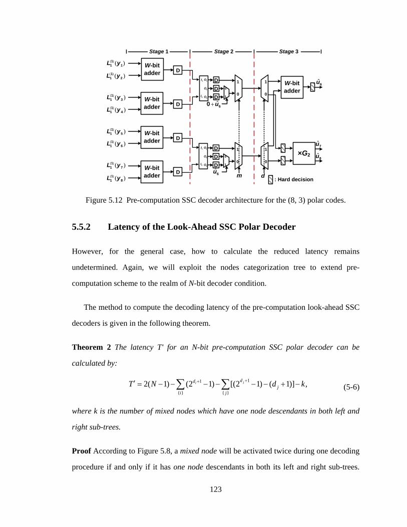
123
u6
Stage 3Stage 2Stage 1
u7
: Hard decision
( ) ( )L y11 1
( ) ( )L y11 2
( ) ( )L y11 3
( ) ( )L y11 4
( ) ( )L y11 5
( ) ( )L y11 6
( ) ( )L y11 7
( ) ( )L y11 8
D
D
D
D
W-bit adder
×G2 u8
W-bit adder
W-bit adder
W-bit adder
W-bit adder
ˆ+u60
u6
1
0
1
0
dm
1
0
1
0
0
1
I1
I2
O1
O2
O3
DDD
0
1
I1
I2
O1
O2
O3
DDD
Figure 5.12 Pre-computation SSC decoder architecture for the (8, 3) polar codes.
Latency of the Look-Ahead SSC Polar Decoder 5.5.2
However, for the general case, how to calculate the reduced latency remains
undetermined. Again, we will exploit the nodes categorization tree to extend pre-
computation scheme to the realm of N-bit decoder condition.
The method to compute the decoding latency of the pre-computation look-ahead SSC
decoders is given in the following theorem.
Theorem 2 The latency T' for an N-bit pre-computation SSC polar decoder can be
calculated by:
11
{ } { }2( 1) (2 1) [(2 1) ( 1)] ,ji dd
ji j
T N d k++′ = − − − − − − + −∑ ∑ (5-6)
where k is the number of mixed nodes which have one node descendants in both left and
right sub-trees.
Proof According to Figure 5.8, a mixed node will be activated twice during one decoding
procedure if and only if it has one node descendants in both its left and right sub-trees.
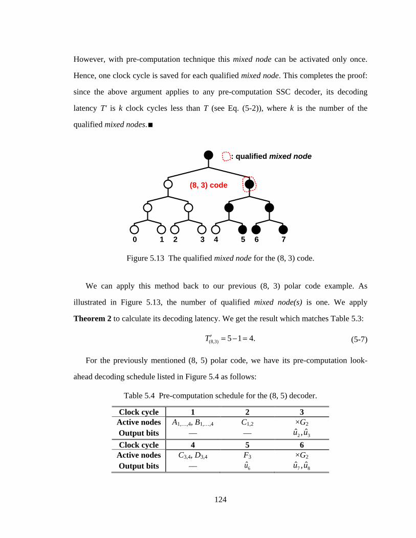
124
However, with pre-computation technique this mixed node can be activated only once.
Hence, one clock cycle is saved for each qualified mixed node. This completes the proof:
since the above argument applies to any pre-computation SSC decoder, its decoding
latency T' is k clock cycles less than T (see Eq. (5-2)), where k is the number of the
qualified mixed nodes.∎
: qualified mixed node
(8, 3) code
0 1 2 3 4 5 6 7
Figure 5.13 The qualified mixed node for the (8, 3) code.
We can apply this method back to our previous (8, 3) polar code example. As
illustrated in Figure 5.13, the number of qualified mixed node(s) is one. We apply
Theorem 2 to calculate its decoding latency. We get the result which matches Table 5.3:
(8,3) 5 1 4.T ′ = − = (5-7)
For the previously mentioned (8, 5) polar code, we have its pre-computation look-
ahead decoding schedule listed in Figure 5.4 as follows:
Table 5.4 Pre-computation schedule for the (8, 5) decoder.
Clock cycle 1 2 3 Active nodes A1,…,4, B1,…,4 C1,2 ×G2 Output bits –– –– 2 3ˆ ˆ,u u Clock cycle 4 5 6
Active nodes C3,4, D3,4 F3 ×G2 Output bits –– 6u 7 8ˆ ˆ,u u

125
: qualified mixed node
0 1 2 3 4 5 6 7
(8, 5) code
Figure 5.14 The qualified mixed node for the (8, 5) code.
According to Figure 5.14, the number of qualified mixed node(s) within the binary
tree is two. By applying Theorem 2 again, we get the result which matches Table 5.4:
(8,5) 8 2 6.T ′ = − = (5-8)
Although the saving here is only one or two clock cycle(s), when N becomes larger,
the positions of one nodes become more scattered, the advantage brought by the pre-
computation method will be more prominent. Please see the 1024-bit polar code in
Section 5.6 as an example.
Latency and Complexity Comparison 5.6
In this section, we compare the proposed SSC polar decoder architectures with state-of-
the-art references. Comparison results of the decoding latency and the hardware
efficiency are listed in Table 5.5 in detail. Since the SSC algorithm is code-aware, here, a
common used (1024, 512) polar code is employed as an example to conduction the
comparison in Table 5.5.

126
Table 5.5 Comparison between the proposed SSC decoders and others.
Different designs Conventional SC decoder† Pre-computation SC
decoder‡ Proposed SSC decoder Proposed pre-computation SSC decoder
Hardware complexity
# of PEs Type I Type II Merged Type I Type II Merged Type I Type II Merged Type I Type II Merged 1023 1023 –– –– –– 1023 1023 1022 –– 7 6 1016
# of matrix mult. block –– –– ×G2 ×G4 ×G2 ×G4
1 1 1 1 # of other REGs 1023W 3068W 1023W 3055W # of other MUXs 0 2045W 12W 2032W
Total XOR 16368W-3069 17390W 16371W-3067 17375W-19 REG 1023W 3068W 1023W+4 3055W+4
Decoding latency Latency 2046 1023 1235 866
†Tree SC decoder proposed in [92]. ‡Pre-computation SC decoder proposed in [58].

127
For the proposed (1024, 512) polar code, there are 258 one node trees with depth 0,
97 with depth 1, and 15 with depth 2, respectively. Meanwhile, there are 258 zero node
trees with depth 0, 97 with depth 1, and 15 with depth 2, respectively. According to
Theorem 1, the latency for the corresponding 1024-bit SSC polar decoder is calculated
as 1235 clock cycles. The number of qualified mixed nodes defined in Theorem 2 is 369.
Hence, the decoding latency for 1024-bit pre-computation SSC polar decoder is 866
clock cycles.
Before the comparison, it is mentioned that the counterpart of the proposed SSC
decoder is the conventional SC tree decoder [92], and the counterpart of the proposed
pre-computation SSC decoder is the pre-computation SC decoder [58]. For hardware
complexity, the word-length of the soft message is W. It is assumed that each 1-bit 2-to-1
multiplexer requires the same silicon area as an XOR gate.
Compared with the conventional SC polar decoder, the proposed SSC one can
achieve 39.6% decoding latency reduction with the same amount of hardware. The
proposed pre-computation SSC decoder requires only 84.6% decoding latency compared
with its SC counterpart, with even lower hardware consumption. Therefore, proposed
SSC polar decoder designs are shown to have advantages in decoding latency compared
with the state-of-the-art designs [36, 58, 59, 92, 94]. For polar codes with long code
lengths and deep one (zero) node trees, this advantage can become more apparent.
Conclusion 5.7
In this chapter, a newly proposed decoding algorithm named SSC algorithm is
investigated. A method to calculate the SSC decoding latency is proposed. Based on the
revised DFG, a design methodology for the SSC polar decoder is given. In order to attain
further reduced decoding latency, the pre-computation look-ahead SSC decoder

128
architecture is also proposed. Comparison results have shown that the proposed
architectures turn out to be very attractive for real-time applications.
Equation Chapter 6 Section 1

129
Chapter 6
Conclusions and Future Research Directions
Conclusions 6.1
This thesis focuses on developing approaches for designing low-latency low-complexity
channel decoder architectures for modern communication systems. Decoding latency (or
throughput) and hardware complexity are the two main focuses of channel decoder
design. How to design a decoder architecture which can well balance the latency and the
hardware is still a challenging problem. In this thesis, we are not only satisfied with
specific decoder designs. Our main goal is to propose a design methodology which is
applicable for general case. With the help of this methodology, we are able to construct
the decoder architecture to meet various design requirements formally.
With the help of VLSI DSP techniques [37], two kinds of channel decoders are
investigated. First, this thesis studies the non-binary QC-LDPC codes. With the given
geometry properties, the low-complexity non-binary QC-LDPC decoder architectures are
proposed. We are able to construct the decoder architecture to meet various design
requirements formally. As a newly proposed error correction code, polar code has shown

130
advantages in several aspects. The rest chapters of this thesis derive several polar decoder
design methodologies for different real-time communication applications.
Non-Binary LDPC Decoders with Efficient Networks 6.1.1
In Chapter 2, the intrinsic shifting and symmetry properties of non-binary QC-LDPC
codes have been exploited. These unique features lead to significant hardware reduction
of the switch networks. With those networks, two low-complexity decoder architectures
are proposed for Class-I and Class-II non-binary QC-LDPC codes, respectively. This
design approach is general and can be applied to other non-binary QC-LDPC decoders.
In order to demonstrate the merits of the proposed method, two design examples are
given. Comparison results with the state-of-the-art designs show that for the code
example of the 64-ary (1260, 630) rate-0.5 Class-I code, the proposed scheme can save
up to 70.6% hardware required by switch network, which demonstrates the efficiency of
the proposed technique. The proposed design for the 32-ary (992, 496) rate-0.5 Class-II
code can achieve a 93.8% switch network complexity reduction compared with
conventional approaches. Furthermore, with the help of a generator for possible solution
sequences, both forward and backward steps can be eliminated to offer processing
convenience of check node unit (CNU) blocks. Results show that the proposed 32-ary
(992, 496) rate-0.5 Class-II decoder can achieve 4.47 Mb/s decoding throughput.
Low-Latency Sequential SC Polar Decoder 6.1.2
Due to their low encoding and decoding complexity, polar codes have recently emerged
as one of the most favorable capacity-achieving error correction codes. However, because
of the large code length required by practical applications, the few existing SC decoder
implementations still suffer from not only high hardware cost but also long decoding
latency.

131
In Chapter 3, a data-flow graph (DFG) for the SC decoder is derived for the first time.
A complete hardware architecture is first derived for the conventional tree SC decoder
and the feedback part is presented next. It is worth noting that the feedback part can be
generated in a systematic way. In order to reduce the decoding latency, pre-computation
look-ahead techniques are proposed based on the DFG analysis. Sub-structure sharing is
used to design a merged PE for higher hardware utilization. Gate-level design details of
the merged PE are provided also. Compared with the conventional N-bit tree SC decoder,
the proposed pre-computation look-ahead decoder architecture can achieve twice speedup
with similar hardware consumption.
High-Throughput SC Polar Decoder Architectures 6.1.3
Two meet the requirements of the modern communication systems, two new SC polar
decoder architectures are proposed in Chapter 4 to achieve higher throughput.
First, a family of TC interleaved pre-computation look-ahead SC polar decoders is
proposed. Several properties of the decoder architectures have been proposed. In order to
meet different throughput requirements for a diverse set of application scenarios,
different versions of the proposed TC interleaved decoders are required. With the help of
those properties, we are able to construct the desired decoder architecture in a systematic
way. Furthermore, when the concurrent parameter M = N-1, the 100% hardware
utilization is achieved. Compared with the conventional N-bit tree SC decoder [28, 92],
the proposed TC interleaved architectures can achieve as high as 2(N-1) times speedup
with only 50% decoding latency and (N∙log2N)/2 merged PEs.
Secondly, a RC interleaved processing approach is also introduced to design polar
decoders. Based on the DFG analysis and the folding technique, the RC L-interleaved
pre-computation look-ahead SC decoder is proposed. The RC 2-interleaved version is

132
used to show the advantage of this approach. Compared with the newly proposed line
decoder design [94], the RC 2-interleaved design can achieve 4 times decoding
throughput with the same hardware cost.
Design of Simplified SC Polar Decoders 6.1.4
The simplified successive cancellation (SSC) algorithm is a revised version of the
conventional SC decoding algorithm. Though it is mathematically equivalent to the SC
decoding algorithm, its decoding latency and hardware cost have been reduced. In
Chapter 5, some problems regarding the SSC polar decoder design issues are discussed.
Since the SSC decoding process highly depends on the specific polar code it is
dealing with, its decoding latency is not trivial to calculate. In this chapter, we present the
first systematic approach to formally derive the SSC decoding latency for any given polar
code. By revising the DFG for the conventional SC decoder, we can easily get the DFG
for the SSC decoder. With this revised DFG, the method to derive various SSC polar
decoder architectures for any specific code is also presented. In order to further reduce
the latency, the pre-computation look-ahead technique is also employed. Similarly, the
latency-reduced SSC decoder’s latency can also be calculated with a simple equation.
Compared with the state-of-the-art SC decoder designs, the two SSC polar decoders can
save up to 39.6% decoding latency with the same hardware cost.
Recently, a low-latency decoding scheme referred as the simplified successive
cancellation (SSC) algorithm has been proposed for the decoding of polar codes. In this
brief, we present the first systematic approach to formally derive the SSC decoding
latency for any given polar code. The method to derive various SSC polar decoder
architectures for any specific code is also presented. Moreover, it is shown that with the
pre-computation technique, the decoding latency can be further reduced. Similarly, the

133
latency-reduced SSC decoder’s latency can also be calculated with a simple equation.
Compared with the state-of-the-art SC decoder designs, the two SSC polar decoders can
save up to 39.6% decoding latency with the same hardware cost.
Future Research Directions 6.2
In the future, we would like to extend our research in the following aspects: (1) extending
our switch network designing methodology to other non-binary QC-LDPC codes; (2)
designing low-latency low-complexity CNU architecture for further non-binary LDPC
decoders; (3) implementing the pre-computation look-ahead SC polar decoder with real
chip; (4) investigating the hardware architectures for the list decoding polar decoders; and
(5) designing the polar decoder architectures for the belief propagation (BP) algorithm.
Switch Networks for Other Non-Binary QC-LDPC Codes 6.2.1
In Chapter 2, the switch networks construction methodology for both Class-I and Class-II
codes. This method leads to significant reduction of memory size and routing complexity.
However, now this method is only applicable for Class-I and Class-II codes.
In the next step, we would like to apply it to other non-binary QC-LDPC codes. The
non-binary QC-LDPC codes form a big family. The previously stated two classes of non-
binary QC-LDPC codes can be categorized into codes constructed in [49]. Usually, the
techniques such as array masking and array dispersion are employed to construct non-
binary QC-LDPC codes. Several useful codes have been proposed by Lingqi’s [46] and
Bo’s [54] PhD dissertations as references. Table 6.1 gives a brief overview of those
popular non-binary QC-LDPC codes. According to the listed construction approaches,
those codes are highly related. Therefore, we can expand our current approach to other
kinds of non-binary QC-LDPC to make this approach more general.

134
Table 6.1 Summary of major non-binary QC-LDPC codes.
Reference Contribution Comment
[47] A general matrix dispersion construction of non-binary QC-LDPC codes based on finite fields is given.
Constriction details can be found in Chapter 3 of [46].
[48] A non-binary incidence-vector construction of non-binary QC-LDPC codes based on finite geometries is proposed.
Constriction details can be found in Chapter 4 of [46]. This is a prior work of [52].
[51] A unified approach for constructing binary and non-binary QC-LDPC codes is presented. This is a prior work of [49].
[52] Construction of non-binary QC-LDPC codes based on flats of finite Euclidean geometries and array masking is presented.
Constriction details can be found in Chapter 5 of [54].
[53] Construction of non-binary QC-LDPC codes based on arrays of circulant matrices and multi-fold array dispersions is presented.
Constriction details can be found in Chapter 4 of [54].
[50] Four specific algebraic constructions of RS-based QC-LDPC codes (construction based on RS codes) are presented.
Constriction details can be found in Chapter 6 of [54].
[49] Construction of non-binary QC-LDPC codes based on dispersing matrices over subgroups of non-binary finite fields is proposed.
Constriction details can be found in Chapter 8 of [54].
135
Low-Latency Low-Complexity CNU Architectures 6.2.2
Similar to their binary counterparts, in the non-binary LDPC decoders, CNU has the
highest hardware complexity among all units. Therefore, low-latency low-complexity
CNU design is the most favorable topic for non-binary decoders [38, 39, 42-44, 68].
Although in Chapter 2, by introducing the generator for possible solution sequences, the
CNU process is simplified, this method is not suitable for 64-ary (or higher order) LDPC
codes since the throughput is too slow to be practical. Also, Because of the inherent high
decoding complexity, the hardware cost of CNU block will increase drastically with the
increase of the finite field order.
Therefore, CNU architectures with low latency and low complexity are still required.
In the next design, we are going to refine the previous path-finding approach to present
an efficient architecture design for the CNU block.
Chip Implementation of the Proposed Polar Decoders 6.2.3
According to Chapter 3 up to Chapter 5, the proposed polar decoder architectures have
shown advantages over previous works. However, the best way to evaluate the decoding
throughput and hardware consumption of one design is to implement it. Also we know
that there are at two published works that provide detailed hardware complexity reports
in FPGA or ASIC [93, 94]. Implementing the proposed designs with prototype would
give a much more clear view of the potential of those works. This would also alleviate
the somehow problematic complexity comparison with the feedback part omitted.
List Decoder Architectures for Polar Codes 6.2.4
In this thesis, all the polar decoders are dealing with SC decoding algorithm, or its
variants, such as Min-Sum algorithm and SSC decoding algorithm. However, the SC

136
decoding algorithm family could not achieve the optimal decoding performance [107].
Recently, the list decoding approach is reported to show better performance compared
with other codes [57]. Until now, no hardware implementation of the list polar decoder
has been reported. Actually, the list decoding algorithm for polar code is nothing but a
multi-way version of the conventional SC decoding followed by a selecting step.
Therefore, the SC decoding algorithm and the list decoding algorithm are highly related.
Our previous design approaches on SC polar decoder architectures can be employed.
Polar Decoders Using Belief Propagation Algorithm 6.2.5
Aside from the SC decoding algorithm, there is another decoding algorithm for polar
codes: the belief propagation (BP) algorithm. This algorithm was first used to give a
performance comparison of polar codes and Reed-Muller codes [34]. In [107], Korada
and Urbanke have proved that SC decoding as a particular instance of BP algorithm. The
performance of BP decoding algorithm is in general superior to that of the SC algorithm.
Also, the corresponding decoding latency is much shorter than that of the SC decoder.
Although the computation complexity of BP decoder is higher than the SC decoder, its
hardware implementation is very attractive for hardware designers.

137
Bibliography
[1] Wikipedia contributors. (13 November 2012 20:48 UTC). Mobile phone. Available: http://en.wikipedia.org/w/index.php?title=Mobile_phone&oldid=521359663
[2] Wikipedia contributors. (13 November 2012 21:10 UTC). China Mobile. Available: http://en.wikipedia.org/w/index.php?title=China_Mobile&oldid=521929749
[3] "IEEE Standard for Air Interface for Broadband Wireless Access Systems," IEEE Std 802.16-2012 (Revision of IEEE Std 802.16-2009), pp. 1-2542, 2012.
[4] Wikipedia contributors. (13 November 2012 21:54 UTC). LTE standard. Available: http://en.wikipedia.org/w/index.php?title=LTE_(telecommunication)&oldid=522856142
[5] Wikipedia contributors. (14 November 2012 23:13 UTC). 3G technologies. Available: http://en.wikipedia.org/w/index.php?title=3G&oldid=522631449
[6] Wikipedia contributors. (13 November 2012 21:44 UTC). 5G technologies. Available: http://en.wikipedia.org/w/index.php?title=5G&oldid=518883254
[7] X. Li, A. Gani, R. Salleh, and O. Zakaria, "The future of mobile wireless communication networks," in Proc. International Conference on Communication Software and Networks (ICCSN), 2009, pp. 554-557.
[8] Wikipedia contributors. (13 November 2012 21:14 UTC). Commun. system. Available: http://en.wikipedia.org/w/index.php?title=Communications_system&oldid=513526649
[9] W. Ryan and S. Lin, Channel Codes: Classical and Modern: Cambridge University Press, 2009.
[10] S. Lin and D. J. Costello, Error Control Coding: Prentice-Hall, Inc., 2004. [11] C. E. Shannon and W. Weaver, The Mathematical Theory of Communication: Univ.
Illinois Press, 1949. [12] T. M. Cover and J. A. Thomas, Elements of Information Theory: Wiley-Interscience,
2006. [13] F. Gray, "Pulse code communication," United States Patent, 1953. [14] R. Hamming, "Error detecting and error correcting codes," Bell System Technical Journal,
vol. 26, pp. 147-160, 1950. [15] I. S. Reed and G. Solomon, "Polynomial codes over certain finite fields," Journal of the
Society for Industrial and Applied Mathematics, vol. 8, pp. 300-304, 1960. [16] A. Hocquenghem, "Codes correcteurs d'erreurs," Chiffres, vol. 2, pp. 147-156, 1959 1959. [17] R. C. Bose and D. K. Ray-Chaudhuri, "On a class of error correcting binary group
codes," Information and Control, vol. 3, pp. 68-79, 3// 1960. [18] C. Berrou, A. Glavieux, and P. Thitimajshima, "Near Shannon limit error-correcting
coding and decoding: Turbo-codes (1)," in Proc. IEEE International Conference on Communications, 1993, pp. 1064-1070 vol.2.
[19] J. W. Byers, M. Luby, M. Mitzenmacher, and A. Rege, "A digital fountain approach to reliable distribution of bulk data," SIGCOMM Comput. Commun. Rev., vol. 28, pp. 56-67, 1998.

138
[20] R. G. Gallager, Low-Density Parity-Check Codes: M.I.T. Press, 1963. [21] "IEEE Standard for Information Technology--Local and Metropolitan Area Networks--
Specific Requirements Part 3," IEEE Std 802.3-2008 (Revision of IEEE Std 802.3-2005), pp. c1-597, 2008.
[22] European Telecommunication Standardization Institute. (14 November 2012 23:13 UTC). Digital Video Broadcasting (DVB)- A guideline for the use of the DVB specifications and standards. Available: http://broadcasting.ru/pdf-standard-specifications/cookbook/dvb-cook/a020r1.pdf
[23] "IEEE Standard for Information technology--Local and metropolitan area networks--Specific requirements Part 11," IEEE Std 802.11-2012 (Revision of IEEE Std 802.11-2007), pp. 1-2793, 2012.
[24] F. Kienle, N. Wehn, and H. Meyr, "On Complexity, Energy- and Implementation-Efficiency of Channel Decoders," IEEE Transactions on Communications, vol. 59, pp. 3301-3310, 2011.
[25] Wikipedia contributors. (15 November 2012 02:14 UTC). Communication. Available: http://en.wikipedia.org/w/index.php?title=Communication&oldid=523065008
[26] M. C. Davey and D. MacKay, "Low-density parity check codes over GF(q)," IEEE Communications Letters, vol. 2, pp. 165-167, 1998.
[27] D. Declercq and M. Fossorier, "Decoding algorithms for nonbinary LDPC codes over GF(q)," IEEE Transactions on Communications, vol. 55, pp. 633-643, 2007.
[28] E. Arikan, "Channel polarization: a method for constructing capacity-achieving codes for symmetric binary-input memoryless channels," IEEE Transactions on Information Theory, vol. 55, pp. 3051-3073, 2009.
[29] S. B. Korada, E. Şaşoğlu, and R. Urbanke, "Polar codes: characterization of exponent, bounds, and constructions," IEEE Transactions on Information Theory, vol. 56, pp. 6253-6264, 2010.
[30] E. Arikan, "Systematic polar coding," IEEE Communications Letters, vol. 15, pp. 860-862, 2011.
[31] R. Mori and T. Tanaka, "Performance of polar codes with the construction using density evolution," IEEE Communications Letters, vol. 13, pp. 519-521, 2009.
[32] S. B. Korada and R. L. Urbanke, "Polar codes are optimal for lossy source coding," IEEE Transactions on Information Theory, vol. 56, pp. 1751-1768, 2010.
[33] O. O. Koyluoglu and H. El Gamal, "Polar coding for secure transmission and key agreement," IEEE Transactions on Information Forensics and Security, vol. 7, pp. 1472-1483, 2012.
[34] E. Arikan, "A performance comparison of polar codes and Reed-Muller codes," IEEE Communications Letters, vol. 12, pp. 447-449, 2008.
[35] H. Mahdavifar and A. Vardy, "Achieving the secrecy capacity of wiretap channels using Polar codes," in Proc. IEEE International Symposium on Information Theory (ISIT), 2010, pp. 913-917.
[36] C. Zhang, B. Yuan, and K. K. Parhi, "Reduced-latency SC polar decoder architectures," in Proc. IEEE International Conference on Communications (ICC), 2012, pp. 3520-3524.
[37] K. K. Parhi, VLSI Digital Signal Processing Systems: Design and Implementation: John Wiley & Sons Inc., 1999.
139
[38] J. Lin, J. Sha, Z. Wang, and L. Li, "An efficient VLSI architecture for nonbinary LDPC decoders," IEEE Transactions on Circuits and Systems II: Express Briefs, vol. 57, pp. 51-55, 2010.
[39] J. Lin, J. Sha, Z. Wang, and L. Li, "Efficient decoder design for nonbinary quasicyclic LDPC codes," IEEE Transactions on Circuits and Systems I: Regular Papers, vol. 57, pp. 1071-1082, 2010.
[40] F. Naessens, A. Bourdoux, and A. Dejonghe, "A flexible ASIP decoder for combined binary and non-binary LDPC codes," in Proc. IEEE Symposium on Communications and Vehicular Technology in the Benelux (SCVT), 2010, pp. 1-5.
[41] A. Voicila, F. Verdier, D. Declercq, M. Fossorier, and P. Urard, "Architecture of a low-complexity non-binary LDPC decoder for high order fields," in Proc. International Symposium on Communications and Information Technologies (ISCIT), 2007, pp. 1201-1206.
[42] X. Zhang and F. Cai, "Partial-parallel decoder architecture for quasi-cyclic non-binary LDPC codes," in Proc. IEEE International Conference on Acoustics Speech and Signal Processing (ICASSP), 2010, pp. 1506-1509.
[43] X. Zhang and F. Cai, "Efficient partial-parallel decoder architecture for quasi-cyclic nonbinary LDPC codes," IEEE Transactions on Circuits and Systems I: Regular Papers, vol. 58, pp. 402-414, 2011.
[44] X. Zhang and F. Cai, "Reduced-complexity decoder architecture for non-binary LDPC codes," IEEE Transactions on Very Large Scale Integration (VLSI) Systems, vol. 19, pp. 1229-1238, 2011.
[45] C. Zhang and K. K. Parhi, "A network-efficient nonbinary QC-LDPC decoder architecture," IEEE Transactions on Circuits and Systems I: Regular Papers, vol. 59, pp. 1359-1371, 2012.
[46] L. Zeng, "Algebraic Constructions of Nonbinary Quasi-Cyclic LDPC Codes and Efficient Encoding," University of California, Davis, 2006.
[47] L. Zeng, L. Lan, Y. Y. Tai, S. Song, S. Lin, and K. Abdel-Ghaffar, "Constructions of nonbinary quasi-cyclic LDPC codes: a finite field approach," IEEE Transactions on Communications, vol. 56, pp. 545-554, 2008.
[48] L. Zeng, L. Lan, Y. Y. Tai, B. Zhou, S. Lin, and K. Abdel-Ghaffar, "Construction of nonbinary cyclic, quasi-cyclic and regular LDPC codes: a finite geometry approach," IEEE Transactions on Communications, vol. 56, pp. 378-387, 2008.
[49] B. Zhou, L. Zhang, J. Kang, Q. Huang, S. Lin, and K. Abdel-Ghaffar, "Array dispersions of matrices and constructions of quasi-cyclic LDPC codes over non-binary fields," in Proc. IEEE International Symposium on Information Theory, 2008, pp. 1158-1162.
[50] B. Zhou, L. Zhang, J. Kang, Q. Huang, Y. Y. Tai, S. Lin, et al., "Non-binary LDPC codes vs. Reed-Solomon codes," in Proc. Information Theory and Applications Workshop, 2008, pp. 175-184.
[51] S. Song, B. Zhou, S. Lin, and K. Abdel-Ghaffar, "A unified approach to the construction of binary and nonbinary quasi-cyclic LDPC codes based on finite fields," IEEE Transactions on Communications, vol. 57, pp. 84-93, 2009.
[52] B. Zhou, J. Kang, Y. Tai, S. Lin, Lin, and Z. Ding, "High performance non-binary quasi-cyclic LDPC codes on Euclidean geometries," IEEE Transactions on Communications, vol. 57, pp. 1298-1311, 2009.

140
[53] B. Zhou, J. Kang, S. Song, S. Lin, K. Abdel-Ghaffar, and M. Xu, "Construction of non-binary quasi-cyclic LDPC codes by arrays and array dispersions," IEEE Transactions on Communications, vol. 57, pp. 1652-1662, 2009.
[54] B. Zhou, "Algebraic Constructions of High Performance and Efficiently Encodable Non-binary Quasi-cyclic LDPC Codes," University of California, Davis, 2008.
[55] K. Jingyu, H. Qin, Z. Li, Z. Bo, and L. Shu, "Quasi-cyclic LDPC codes: an algebraic construction," IEEE Transactions on Communications, vol. 58, pp. 1383-1396, 2010.
[56] Z. Bo, Y. Y. Tai, L. Lan, S. Song, Z. Lingqi, and L. Shu, "Construction of high performance and efficiently encodable nonbinary quasi-cyclic LDPC codes," in Proc. Global Telecommunications Conference (GLOBECOM), 2006, pp. 1-6.
[57] I. Tal and A. Vardy. (2012, May 1, 2012). List decoding of polar codes. ArXiv e-prints 1206, 50. Available: http://adsabs.harvard.edu/abs/2012arXiv1206.0050T
[58] C. Zhang and K. K. Parhi, "Low-latency sequential and overlapped architectures for successive cancellation polar decoder," IEEE Transactions on Signal Processing, in revision.
[59] C. Zhang and K. K. Parhi, "Interleaved successive cancellation polar decoders," in Proc. IEEE International Conference on Acoustics Speech and Signal Processing (ICASSP), 2013, submitted.
[60] A. Alamdar-Yazdi and F. R. Kschischang, "A simplified successive-cancellation decoder for polar codes," IEEE Communications Letters, vol. 15, pp. 1378-1380, 2011.
[61] C. Zhang and K. K. Parhi, "Latency analysis and architecture design of simplified SC polar decoders," IEEE Transactions on Circuits and Systems II: Express Briefs, in revision.
[62] D. J. C. MacKay and R. M. Neal, "Near Shannon limit performance of low density parity check codes," Electronics Letters, vol. 33, pp. 457-458, 1997.
[63] "IEEE Standard for Information technology--Specific requirements-- Part 11:," IEEE Std 802.11n-2009 (Amendment to IEEE Std 802.11-2007 as amended by IEEE Std 802.11k-2008, IEEE Std 802.11r-2008, IEEE Std 802.11y-2008, and IEEE Std 802.11w-2009), pp. 1-565, 2009.
[64] "IEEE Standard for Local and Metropolitan Area Networks Part 16: Air Interface for Fixed and Mobile Broadband Wireless Access Systems Amendment 2," IEEE Std 802.16e-2005 and IEEE Std 802.16-2004/Cor 1-2005 (Amendment and Corrigendum to IEEE Std 802.16-2004), pp. 0_1-822, 2006.
[65] SARFT. (15 November 2012 22:14 UTC). China Mobile Multimedia Broadcasting (CMMB). Available: http://www.cmmb.org.cn/
[66] DTMB. (15 November 2012 22:14 UTC). Framing Structure, Channel Coding and Modulation for Digital Television Tterrestrial Broadcasting System (DTTV). Available: http://www.sac.gov.cn/SACSearch/outlinetemplet/gjcxjg_qwyd.jsp?bzNum=GB20600-2006
[67] H. Wymeersch, H. Steendam, and M. Moeneclaey, "Log-domain decoding of LDPC codes over GF(q)," in Proc. IEEE International Conference on Communications, 2004, pp. 772-776.
[68] C. Spagnol, E. M. Popovici, and W. P. Marnane, "Hardware implementation of GF(2m) LDPC decoders," IEEE Transactions on Circuits and Systems I: Regular Papers, vol. 56, pp. 2609-2620, 2009.

141
[69] A. Voicila, D. Declercq, F. Verdier, M. Fossorier, and P. Urard, "Low-complexity decoding for non-binary LDPC codes in high order fields," IEEE Transactions on Communications, vol. 58, pp. 1365-1375, 2010.
[70] E. Boutillon and L. Conde-Canencia, "Bubble check: a simplified algorithm for elementary check node processing in extended min-sum non-binary LDPC decoders," Electronics Letters, vol. 46, pp. 633-634, 2010.
[71] V. Savin, "Min-Max decoding for non binary LDPC codes," in Proc. IEEE International Symposium on Information Theory (ISIT), 2008, pp. 960-964.
[72] D. Oh and K. K. Parhi, "Min-Sum decoder architectures with reduced word length for LDPC codes," IEEE Transactions on Circuits and Systems I: Regular Papers, vol. 57, pp. 105-115, 2010.
[73] D. Oh and K. K. Parhi, "Low-complexity switch network for reconfigurable LDPC decoders," IEEE Transactions on Very Large Scale Integration (VLSI) Systems, vol. 18, pp. 85-94, 2010.
[74] D. Oh and K. Parhi, "Low complexity decoder architecture for low-density parity-check codes," Journal of Signal Processing Systems, vol. 56, pp. 217-228, 2009.
[75] Z. Cui, Z. Wang, and Y. Liu, "High-throughput layered LDPC decoding architecture," IEEE Transactions on Very Large Scale Integration (VLSI) Systems, vol. 17, pp. 582-587, 2009.
[76] Z. Cui and Z. Wang, "Extended layered decoding of LDPC codes," in Proc. ACM Great Lakes symposium on VLSI, Orlando, Florida, USA, 2008, pp. 457-462.
[77] T. Lehnigk-Emden and N. Wehn, "Complexity evaluation of non-binary Galois field LDPC code decoders," in Proc. International Symposium on Turbo Codes and Iterative Information, 2010, pp. 53-57.
[78] S. Zhou, J. Sha, L. Li, and Z. Wang, "Layered decoding for non-binary LDPC codes," in Proc. IEEE International Symposium on Circuits and Systems (ISCAS), 2010, pp. 481-484.
[79] D. Oh and K. K. Parhi, "Area efficient controller design of barrel shifters for reconfigurable LDPC decoders," in Proc. IEEE International Symposium on Circuits and Systems (ISCAS), 2008, pp. 240-243.
[80] J. Tang, T. Bhatt, V. Sundaramurthy, and K. K. Parhi, "Reconfigurable shuffle network design in LDPC decoders," in Proc. International Conference on Application-specific Systems, Architectures and Processors (ASAP), 2006, pp. 81-86.
[81] C. Y. Lee and J. M. Tsai, "A shift register architecture for high-speed data sorting," Journal of VLSI Signal Processing, vol. 11, pp. 273-280, Dec 1995.
[82] C. Berrou and A. Glavieux, "Near optimum error correcting coding and decoding: turbo-codes," IEEE Transactions on Communications, vol. 44, pp. 1261-1271, 1996.
[83] P. Robertson, "Illuminating the structure of code and decoder of parallel concatenated recursive systematic (turbo) codes," in Proc. IEEE Global Telecommunications Conference (GLOBECOM), 1994, pp. 1298-1303 vol.3.
[84] D. Arnold and G. Meyerhans, The Realization of the Turbo-Coding System: Swiss Fed. Inst. of Tech., 1995.
[85] R. Tanner, "A recursive approach to low complexity codes," IEEE Transactions on Information Theory, vol. 27, pp. 533-547, 1981.

142
[86] D. J. C. MacKay, "Good error-correcting codes based on very sparse matrices," in Proc. IEEE International Symposium on Information Theory, 1997, p. 113.
[87] M. Garrido, K. K. Parhi, and J. Grajal, "A pipelined FFT architecture for real-valued signals," IEEE Transactions on Circuits and Systems I: Regular Papers, vol. 56, pp. 2634-2643, 2009.
[88] P. Robertson, E. Villebrun, and P. Hoeher, "A comparison of optimal and sub-optimal MAP decoding algorithms operating in the log domain," in Proc. IEEE International Conference on Communications (ICC), 1995, pp. 1009-1013 vol.2.
[89] F. R. Kschischang, B. J. Frey, and H. A. Loeliger, "Factor graphs and the sum-product algorithm," IEEE Transactions on Information Theory, vol. 47, pp. 498-519, 2001.
[90] Z. Wang and K. K. Parhi, "High performance, high throughput turbo/SOVA decoder design," IEEE Transactions on Communications, vol. 51, pp. 570-579, 2003.
[91] Z. Wang, Z. Chi, and K. K. Parhi, "Area-efficient high-speed decoding schemes for turbo decoders," IEEE Transactions on Very Large Scale Integration (VLSI) Systems, vol. 10, pp. 902-912, 2002.
[92] C. Leroux, I. Tal, A. Vardy, and W. J. Gross, "Hardware architectures for successive cancellation decoding of polar codes," in Proc. IEEE International Conference on Acoustics, Speech and Signal Processing (ICASSP), 2011, pp. 1665-1668.
[93] A. Pamuk, "An FPGA implementation architecture for decoding of polar codes," in International Symposium on Wireless Communication Systems (ISWCS), 2011, pp. 437-441.
[94] C. Leroux, A. J. Raymond, G. Sarkis, I. Tal, A. Vardy, and W. J. Gross, "Hardware implementation of successive-cancellation decoders for polar codes," Journal of Signal Processing Systems for Signal Image and Video Technology, vol. 69, pp. 305-315, Dec 2012.
[95] E. A. Lee and D. G. Messerschmitt, "Static scheduling of synchronous data flow programs for digital signal processing," IEEE Transactions on Computers, vol. C-36, pp. 24-35, 1987.
[96] K. Ito and K. K. Parhi, "Determining the minimum iteration period of an algorithm," J. VLSI Signal Process. Syst., vol. 11, pp. 229-244, 1995.
[97] K. Ito, L. E. Lucke, and K. K. Parhi, "ILP-based cost-optimal DSP synthesis with module selection and data format conversion," IEEE Transactions on Very Large Scale Integration (VLSI) Systems, vol. 6, pp. 582-594, 1998.
[98] T. C. Denk and K. K. Parhi, "Synthesis of folded pipelined architectures for multirate DSP algorithms," IEEE Transactions on Very Large Scale Integration (VLSI) Systems, vol. 6, pp. 595-607, 1998.
[99] K. K. Parhi, "Pipelining in algorithms with quantizer loops," IEEE Transactions on Circuits and Systems, vol. 38, pp. 745-754, 1991.
[100] K. K. Parhi and D. G. Messerschmitt, "Pipeline interleaving and parallelism in recursive digital filters, part I: Pipelining using scattered look-ahead and decomposition," IEEE Transactions on Acoustics, Speech and Signal Processing, vol. 37, pp. 1099-1117, 1989.
[101] K. K. Parhi and D. G. Messerschmitt, "Pipeline interleaving and parallelism in recursive digital filters, part II: Pipelined incremental block filtering," IEEE Transactions on Acoustics, Speech and Signal Processing, vol. 37, pp. 1118-1134, 1989.

143
[102] Wikipedia contributors. (14 November 2012 20:33 UTC). Adder-subtractor. Available: http://en.wikipedia.org/w/index.php?title=Adder%E2%80%93subtractor&oldid=515321310
[103] Wikipedia contributors. (14 November 2012 20:41 UTC). Kronecker product. Available: http://en.wikipedia.org/w/index.php?title=Kronecker_product&oldid=509224913
[104] K. K. Parhi and D. G. Messerschmitt, "Static rate-optimal scheduling of iterative data-flow programs via optimum unfolding," IEEE Transactions on Computers, vol. 40, pp. 178-195, 1991.
[105] M. Ayinala, M. Brown, and K. K. Parhi, "Pipelined parallel FFT architectures via folding transformation," IEEE Transactions on Very Large Scale Integration (VLSI) Systems, vol. 20, pp. 1068-1081, 2012.
[106] V. Sundararajan and K. K. Parhi, "Synthesis of low power folded programmable coefficient FIR digital filters," in Proc. Asia and South Pacific Design Automation Conference, 2000, pp. 153-156.
[107] S. B. Korada, "Polar Codes for Channel and Source Coding," EPFL, 2009.