ktfrdm-mc12xsfug, frdm-17xsf5-evb, frdm...
TRANSCRIPT

KTFRDM–MC12XSFUGFRDM-17XSF5-EVB, FRDM-17XSF4-EVB, FRDM-08XSF4-EVBand FRDM-40XSF5-EVB evaluation boardsRev. 1 — 5 May 2016 User guide
1 FRDM-17XSF5-EVB
NXP Semiconductors KTFRDM–MC12XSFUGFRDM-17XSF5-EVB, FRDM-17XSF4-EVB, FRDM-08XSF4-EVB and FRDM-40XSF5-EVB evaluation boards
KTFRDM–MC12XSFUG All information provided in this document is subject to legal disclaimers. © NXP B.V. 2016. All rights reserved
User guide Rev. 1 — 5 May 20162 / 23
2 Important notice
NXP provides the enclosed product(s) under the following conditions:
This evaluation kit is intended for use of ENGINEERING DEVELOPMENT OREVALUATION PURPOSES ONLY. It is provided as a sample IC pre-soldered to aprinted circuit board to make it easier to access inputs, outputs, and supply terminals.This evaluation board may be used with any development system or other source ofI/O signals by simply connecting it to the host MCU or computer board via off-the-shelf cables. This evaluation board is not a Reference Design and is not intended torepresent a final design recommendation for any particular application. Final device inan application will be heavily dependent on proper printed circuit board layout and heatsinking design as well as attention to supply filtering, transient suppression, and I/Osignal quality.
The goods provided may not be complete in terms of required design, marketing, andor manufacturing related protective considerations, including product safety measurestypically found in the end product incorporating the goods. Due to the open constructionof the product, it is the user's responsibility to take any and all appropriate precautionswith regard to electrostatic discharge. In order to minimize risks associated with thecustomers applications, adequate design and operating safeguards must be providedby the customer to minimize inherent or procedural hazards. For any safety concerns,contact NXP sales and technical support services.
Should this evaluation kit not meet the specifications indicated in the kit, it may bereturned within 30 days from the date of delivery and will be replaced by a new kit.
NXP reserves the right to make changes without further notice to any products herein.NXP makes no warranty, representation or guarantee regarding the suitability of itsproducts for any particular purpose, nor does NXP assume any liability arising out of theapplication or use of any product or circuit, and specifically disclaims any and all liability,including without limitation consequential or incidental damages. “Typical” parameterscan and do vary in different applications and actual performance may vary over time.All operating parameters, including “Typical”, must be validated for each customerapplication by customer’s technical experts.
NXP does not convey any license under its patent rights nor the rights of others. NXPproducts are not designed, intended, or authorized for use as components in systemsintended for surgical implant into the body, or other applications intended to support orsustain life, or for any other application in which the failure of the NXP product couldcreate a situation where personal injury or death may occur.
Should the Buyer purchase or use NXP products for any such unintended orunauthorized application, the Buyer shall indemnify and hold NXP and its officers,employees, subsidiaries, affiliates, and distributors harmless against all claims, costs,damages, and expenses, and reasonable attorney fees arising out of, directly orindirectly, any claim of personal injury or death associated with such unintended orunauthorized use, even if such claim alleges NXP was negligent regarding the designor manufacture of the part. NXP and the NXP logo are trademarks of NXP B.V. All otherproduct or service names are the property of their respective owners. © 2016 NXP B.V.
NXP Semiconductors KTFRDM–MC12XSFUGFRDM-17XSF5-EVB, FRDM-17XSF4-EVB, FRDM-08XSF4-EVB and FRDM-40XSF5-EVB evaluation boards
KTFRDM–MC12XSFUG All information provided in this document is subject to legal disclaimers. © NXP B.V. 2016. All rights reserved
User guide Rev. 1 — 5 May 20163 / 23
3 Getting started
3.1 Kit contents/packing listThe FRDM-17XSF5-EVB, FRDM-17XSF4-EVB, FRDM-08XSF4-EVB andFRDM-40XSF5-EVB contents include:
• Assembled and tested evaluation board/module in anti-static bag• Connector 1x2 for power supply• Connector 1x6 for loads• Quick start guide• Warranty card
3.2 Jump startNXP’s analog product development boards provide an easy-to-use platform forevaluating NXP products. The boards support a range of analog, mixed-signal and powersolutions. They incorporate monolithic ICs and system-in-package devices that useproven high-volume SMARTMOS technology. NXP products offer longer battery life, asmaller form factor, reduced component counts, lower cost and improved performance inpowering state of the art systems.
1. Go to http://www.nxp.com/FRDM-MC12XSF.2. Review your Tools Summary Page.3. Locate and click:
4. Download the documents, software, and other information.
Once the files are downloaded, review the user guide in the bundle. The user guideincludes setup instructions, BOM and schematics. Jump start bundles are available oneach tool summary page with the most relevant and current information. The informationincludes everything needed for design.
3.3 Required equipmentThis kit requires the following items:
• Power supply 7.0 to 18 V• Typical loads (DC motor, LED, bulb)• One of the following MCU boards:
– FRDM-KL25Z– FRDM-K64F– FRDM-KV10Z
• SPIGen• CodeWarrior 10.6 or higher, Kinetis Design Studio 3.0.0 or higher, Driver Suite 10.4 or
higher, Processor Expert version RT6 or higher
NXP Semiconductors KTFRDM–MC12XSFUGFRDM-17XSF5-EVB, FRDM-17XSF4-EVB, FRDM-08XSF4-EVB and FRDM-40XSF5-EVB evaluation boards
KTFRDM–MC12XSFUG All information provided in this document is subject to legal disclaimers. © NXP B.V. 2016. All rights reserved
User guide Rev. 1 — 5 May 20164 / 23
3.4 System requirementsThe kit requires the following to function properly with the software:
• USB-enabled PC with Windows® XP or higher
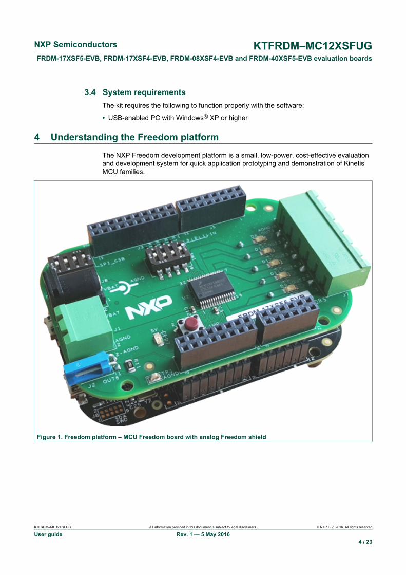
4 Understanding the Freedom platform
The NXP Freedom development platform is a small, low-power, cost-effective evaluationand development system for quick application prototyping and demonstration of KinetisMCU families.
Figure 1. Freedom platform – MCU Freedom board with analog Freedom shield

NXP Semiconductors KTFRDM–MC12XSFUGFRDM-17XSF5-EVB, FRDM-17XSF4-EVB, FRDM-08XSF4-EVB and FRDM-40XSF5-EVB evaluation boards
KTFRDM–MC12XSFUG All information provided in this document is subject to legal disclaimers. © NXP B.V. 2016. All rights reserved
User guide Rev. 1 — 5 May 20165 / 23
5 Getting to know the hardware
5.1 Board overviewThe FRDM-17XSF5-EVB, FRDM-17XSF4-EVB, FRDM-08XSF4-EVB andFRDM-40XSF5-EVB evaluation boards feature one of the ICs belonging to NXP’s 12XSFhigh-side switch products family.
The board incorporates up to 5 outputs with freewheeling diode protection and LEDindication, external smart power switch control output, on-board voltage regulator andlevel shifter (from 3.3 V to 5.0 V logic) and switch to enable operation of up to four boardsin parallel with separate chip-select pins (parallel SPI operation).
5.2 Device features12XSF family of eXtreme switch products is the latest achievement in DC motors andautomotive/industrial lighting drivers. The products belong to an expanding family tocontrol and diagnose various types of loads, such as incandescent bulbs or light emittingdiodes (LEDs), with enhanced precision.
The products combine flexibility through daisy-chainable SPI at 5.0 MHz, extended digitaland analog feedbacks, which supports safety and robustness.
This fourth generation of NXP's high-side switch products family facilitates electroniccontrol unit designs supported by the use of compatible MCU software and PCBfootprints, for each device variant.
Common features of 12XSF family:
• Operating voltage range of 7.0 V to 18 V, with sleep current < 5.0 µA• 5.0 MHz 16-bit SPI control of overcurrent profiles, channel control including 8-bit PWM
duty-cycles, output ON and OFF open load detections, thermal shutdown and pre-warning and fault reporting
• Output current monitoring with programmable synchronization signal and supplyvoltage feedback
• Programmable overcurrent trip levels• Watchdog and limp home mode• External smart power switch control (output 6)• −16 V reverse polarity and ground disconnect protections• Compatible PCB foot print and SPI software driver among the family
The 12XSF family products differ in number of available outputs and its RDS(on)resistance. The ICs present on one of the Freedom evaluation boards are in Table 1.
Table 1. Device featuresProduct number No. of
outputsOUT1 OUT2 OUT3 OUT4 OUT5 OUT6
MC08XSF421 4 + 1 21 mΩ 21 mΩ 8 mΩ 8 mΩ N.C Yes
MC17XSF400 4 + 1 17 mΩ 17 mΩ 17 mΩ 17 mΩ N.C Yes
MC17XSF500 5 + 1 17 mΩ 17 mΩ 17 mΩ 17 mΩ 17 mΩ Yes
MC40XSF500 5 + 1 40 mΩ 40 mΩ 40 mΩ 40 mΩ 40 mΩ Yes

NXP Semiconductors KTFRDM–MC12XSFUGFRDM-17XSF5-EVB, FRDM-17XSF4-EVB, FRDM-08XSF4-EVB and FRDM-40XSF5-EVB evaluation boards
KTFRDM–MC12XSFUG All information provided in this document is subject to legal disclaimers. © NXP B.V. 2016. All rights reserved
User guide Rev. 1 — 5 May 20166 / 23
5.3 Board descriptionFigure 2 describes the main blocks of the evaluation board.
2
3
4
1
5 6 7 8 9
10
11
12
13
14
15
17 161819
Figure 2. Freedom board overview (without load)
Table 2. Freedom board overviewNumber Description
1 SW2 CS pin selection
2 Connector J8 (Power supply)
3 Connector J1 (Power supply)
4 Connector J2 (OUT6)
5 5.0 V power supply LED
6 LIMP button
7 Connector J4
8 Connector J6
9 Output LEDs
10 Connector J7 (OUT2)
11 Connector J7 (OUT4)
12 Connector J7 (OUT5)
13 Connector J7 (OUT3)
14 Connector J7 (OUT1)
15 Connector J7 (GND)
16 MC17XSF500 IC
17 Connector J5

NXP Semiconductors KTFRDM–MC12XSFUGFRDM-17XSF5-EVB, FRDM-17XSF4-EVB, FRDM-08XSF4-EVB and FRDM-40XSF5-EVB evaluation boards
KTFRDM–MC12XSFUG All information provided in this document is subject to legal disclaimers. © NXP B.V. 2016. All rights reserved
User guide Rev. 1 — 5 May 20167 / 23
Number Description18 Connector J3
19 SW1 Direct control inputs
5.3.1 LEDsThe following LEDs are provided as visual output devices for the board:
Table 3. LED descriptionLED identifier Description
D7 5 V power supply present (voltage regulator output)
D8 Output 1
D9 Output 2
D10 Output 3
D11 Output 4
D12 Output 5
5.3.2 ConnectorsInput/output connectors provide the following signals:
Table 4. Connectors descriptionConnector identifier Description
J1 VBAT Power (and AGND) connector
J2 External smart power switch control output (and AGND)connector
J3 2x10 Freedom board header
J4 2x8 Freedom board header
J5 2x8 Freedom board header
J6 2x6 Freedom board header
J7 Output 1 to 5 (and AGND) connector
J8 VBAT Power (and AGND) 5.5/2.1 mm socket

NXP Semiconductors KTFRDM–MC12XSFUGFRDM-17XSF5-EVB, FRDM-17XSF4-EVB, FRDM-08XSF4-EVB and FRDM-40XSF5-EVB evaluation boards
KTFRDM–MC12XSFUG All information provided in this document is subject to legal disclaimers. © NXP B.V. 2016. All rights reserved
User guide Rev. 1 — 5 May 20168 / 23
5.3.3 Switches definitionThe following table defines the evaluation board switches and explains their functions:
Table 5. Switches definitionSwitch Description Setting Connection
ON Corresponding channel is onwhen direct inputs are usedand no level on MCU pin isset
SW1 Direct control inputs foroutputs 1 to 4
OFF Corresponding channel is offwhen direct inputs are usedand no level on MCU pin isset
1 ON, other OFF CSB3 used as chip-select pin
2 ON, other OFF CSB2 used as chip-select pin
3 ON, other OFF CSB1 used as chip-select pin
SW2 Chip-select pin selection
4 ON, other OFF CSB0 used as chip-select pin
5.3.4 Test point definitionThe following test point provides access to various signals to and from the board:
Table 6. Test point definitionTest point Signal name Description
TP1 AGND Common ground for both MCU and analog Freedom board
5.3.5 Freedom board headersTable 7 contains information about compatibility with selected MCU Freedom boards:
Table 7. Compatibility with selected MCU Freedom boardsFRDM-12XSF-EVB Pin description FRDM-KL25Z FRDM-K64F FRDM-KV10Z
J3 1 RSTB_FRDM eXtreme Switch reset J2 1 PTC12 J2 1 PTE26 J2 1 PTE18
J3 3 IN1 Direct control input 1 J2 3 PTC13 J2 3 X J2 3 PTB1
J3 5 IN2 Direct control input 2 J2 5 PTC16 J2 5 X J2 5 PTE19
J3 6 CSB0 Chip-select 0 J2 6 PTD0 J2 6 PTD0 J2 6 PTD6
J3 7 IN3 Direct control input 3 J2 7 PTC17 J2 7 X J2 7 PTE17
J3 8 MOSI SPI MOSI data J2 8 PTD2 J2 8 PTD2 J2 8 PTC6
J3 9 IN4 Direct control input 4 J2 9 PTA16 J2 9 X J2 9 PTE30
J3 10 MISO SPI MISO data J2 10 PTD3 J2 10 PTD3 J2 10 PTD3
J3 12 CLK SPI clock J2 12 PTD1 J2 12 PTD1 J2 12 PTC5
J3 13 CSB1 Chip-select 1 J2 13 PTE31 J2 13 X J2 13 X
J3 18 CSB3 Chip-select 3 J2 18 PTE0 J2 18 X J2 18 X
J3 19 CSB2 Chip-select 2 J2 19 PTD7 J2 19 X J2 19 X
J5 5 CLK_FRDM External clock for PWM J1 5 PTC3 J1 5 PTC1 J1 5 PTE25
J5 6 CSNS_SYNC Monitoring synchronization J1 6 PTD4 J1 6 PTB9 J1 6 X
J6 6 CSNS Monitoring output J10 6 PTB2 J4 6 PTB10 J4 6 X
NXP Semiconductors KTFRDM–MC12XSFUGFRDM-17XSF5-EVB, FRDM-17XSF4-EVB, FRDM-08XSF4-EVB and FRDM-40XSF5-EVB evaluation boards
KTFRDM–MC12XSFUG All information provided in this document is subject to legal disclaimers. © NXP B.V. 2016. All rights reserved
User guide Rev. 1 — 5 May 20169 / 23
6 Installing the software and setting up the hardware
6.1 Using SPIGen software
6.1.1 Installing SPIGen freeware on your computerThe latest version of SPIGen is designed to run on Windows 8, Windows 7, Vista or XP-based operating systems.
To install the software, go to http://www.nxp.com/FRDM-MC12XSF. Locate and clickJump Start Your Design.
1. Download the SPIGen software as well as the associated configuration file.2. Run the install program from the desktop. The Installation Wizard conducts the rest of
the process.3. To use SPIGen, go to the Windows Start menu, Programs, SPIGen, and then click
on the SPIGen icon. The SPIGen Graphic User Interface (GUI) appears.4. Go to the file menu in the upper left hand corner of the GUI, and select Open. Browse
for the configuration file that was saved on the desktop earlier with the Jump start andselect it (“12XSF_SPIGEN_eval.spi”), then click Open.
5. The GUI shown in Figure 3 presents some basic SPI commands for quick evaluationof 12XSF devices in addition with access to I/Os with Extra pins. The commands aresent once (single command) or continuously in a loop (batch command).

NXP Semiconductors KTFRDM–MC12XSFUGFRDM-17XSF5-EVB, FRDM-17XSF4-EVB, FRDM-08XSF4-EVB and FRDM-40XSF5-EVB evaluation boards
KTFRDM–MC12XSFUG All information provided in this document is subject to legal disclaimers. © NXP B.V. 2016. All rights reserved
User guide Rev. 1 — 5 May 201610 / 23
Figure 3. SPIGen GUI
6.1.2 Connecting FRDM-KL25Z Freedom Development PlatformFRDM-17XSF5-EVB can be used with KL25Z Freedom board using SPIGEN software.An USB cable from a USB host connected to KL25Z mini-B USB connector, SPIGEN (7.xand above) and a power supply are needed to use the kit.
Installing the drivers
To flash the Freedom board using drag and drop from Windows Explorer, USB Driversand OpenSDA Firmware (MSD & Debug) from P&E Micro http://www.pemicro.com/opensda must be loaded on the board.
1. Enter OpenSDA Bootloader ModeUnplug the USB cable if attached. Press and hold the Reset button (SW1). Plug ina USB cable between a USB host and the OpenSDA USB connector. Release theReset button. A removable drive is visible in the host file system with a volume label ofBOOTLOADER. You are now in OpenSDA Bootloader mode.
2. Load an OpenSDA ApplicationLocate the OpenSDA Applications folder from the downloaded zip file. Copy andpaste or drag and drop the MSD Flash Programmer Application (MSD-FRDM-

NXP Semiconductors KTFRDM–MC12XSFUGFRDM-17XSF5-EVB, FRDM-17XSF4-EVB, FRDM-08XSF4-EVB and FRDM-40XSF5-EVB evaluation boards
KTFRDM–MC12XSFUG All information provided in this document is subject to legal disclaimers. © NXP B.V. 2016. All rights reserved
User guide Rev. 1 — 5 May 201611 / 23
KL25Z_vXYZ_Pemicro.SDA) to the BOOTLOADER drive (Make sure to unzip the filebefore doing the paste or drop). Unplug the USB cable and plug it again into the SDAUSB Connector. The new OpenSDA Application is now running and a FRDM-KL25Zdrive visible in the host file system.
3. Enter OpenSDA Bootloader ModeLocate SPIGEN UsbSpiDongleKL25Z_XXX.srec image folder in SPIGEN folder (C:\Program Files (x86)\SPIGen\SPI Dongle Firmware). Copy and paste or drag anddrop the .srec files to the FRDM-KL25Z drive. Unplug the USB cable for the openSDA USB Connector and plug it to the USB_KL25Z.
6.1.3 Setting up the hardware using SPIGenTo perform the examples included in the software bundle, the following connections andsetup must be performed:
1. Attach the +12 VDC supply to the VBAT input connector on the FRDM-17XSF5-EVBon J8 or J1 (making sure to observe the GND and +12 V terminals). The currentcapability of the +12 V supply should exceed the maximum total current that thenumber of simultaneously ON loads require.
2. Attach loads to the output terminals (OUT1..5).3. Turn on the +12 V supply. Verify all is working correctly by observing the +5.0 V LED
D7, which should be illuminated. .4. Connect the KL25Z to the PC using the USB KL25Z port (left side of SW1). The
hardware connection is shown in Figure 4. A window pops up on the SPIGEN GUI asshown in Figure 5.
Figure 4. Hardware setup

NXP Semiconductors KTFRDM–MC12XSFUGFRDM-17XSF5-EVB, FRDM-17XSF4-EVB, FRDM-08XSF4-EVB and FRDM-40XSF5-EVB evaluation boards
KTFRDM–MC12XSFUG All information provided in this document is subject to legal disclaimers. © NXP B.V. 2016. All rights reserved
User guide Rev. 1 — 5 May 201612 / 23
Figure 5. FRDM-KL25Z connected
6.1.4 Running the example batch files1. Make sure that bundle 12XSF_SPIGEN_eval.spi is loaded on your SPIGEN interface.2. Go to the Batch commands page and select the batch file you want to run. There are
some choices that allows to Turn ON some outputs, simply refresh the Watchdog andread register, or root the IC’s temperature to the analog pin CSNS. Click on the SendContinuously button.
3. Observe the desire effect on the outputs or on analog feedback pin CSNS. Note thatwe can force Fail-safe mode during the SPI communication by pushing LIMP buttonon board (SW3).
6.2 Using Kinetis Design Studio and Processor ExpertThe Gen4eXtremeSwitch component for 12XSF and 12XS6 handles initialization, run-time configuration and diagnosis of the device via SPI, feedback measurement and directinput control.
The component package contains various examples showing features of both thecomponent and the device. The component and some examples in the componentpackage are intended for Kinetis Design Studio 3.2.0. For more information aboutGen4eXtremeSwitch component, Processor Expert and installation of KinetisDesign Studio, see Gen4eXtremeSwitch component user guide available at http://www.nxp.com/GEN4-EXTREMESWITCH-PEXPERT.

NXP Semiconductors KTFRDM–MC12XSFUGFRDM-17XSF5-EVB, FRDM-17XSF4-EVB, FRDM-08XSF4-EVB and FRDM-40XSF5-EVB evaluation boards
KTFRDM–MC12XSFUG All information provided in this document is subject to legal disclaimers. © NXP B.V. 2016. All rights reserved
User guide Rev. 1 — 5 May 201613 / 23
7 Schematics
7.1 FRDM-17XSF5-EVB
5 5
4 4
3 3
2 2
1 1
DD
CC
BB
AA
Level Shifter
FRDM
RS
TB
SP
I0_C
SB
CLK
SP
I0_C
LKS
PI0
_MO
SI
SP
I0_M
ISO
CS
NS
_SY
NC
B
CS
NS
OU
T_6
LIM
P
IN1
IN2
IN3
SP
I0_C
SB
1
SP
I0_C
SB
2
OUT_2OUT_4OUT_5OUT_3OUT_1
OU
T_6
SP
I0_C
SB
3S
PI0
_CS
B2
SP
I0_C
SB
1S
PI0
_CS
B0
OU
T_3
OU
T_2
OU
T_1
SP
I0_C
SB
_FR
DM
SP
I0_M
OS
I_F
RD
M
SP
I0_C
LK_F
RD
M
RS
TB
_FR
DM
SP
I0_C
SB
SP
I0_M
OS
I
SP
I0_C
LK
RS
TB
RS
TB
_FR
DM
IN4
CLK
_FR
DM
CLK
_FR
DM
IN2
IN3
IN4
OU
T_5
OU
T_4
OU
T_1
OU
T_2
OU
T_3
OU
T_4
OU
T_5
SP
I0_C
SB
_FR
DM
IN1
CLK
SP
I0_C
SB
0S
PI0
_MO
SI_
FR
DM
SP
I0_M
ISO
_FR
DM
SP
I0_C
SB
3
SP
I0_C
LK_F
RD
M
CS
NS
CS
NS
_SY
NC
B
SP
I0_M
ISO
SP
I0_M
ISO
_FR
DM
AG
ND
AG
ND
AG
ND
AG
ND
AG
ND
AG
ND
AG
ND
AG
ND
AG
ND
AG
ND
5V
AG
ND
AG
ND
AG
ND
AG
ND
AG
ND
AG
ND
AG
ND
AG
ND
AG
ND
AG
ND
AG
ND
AG
ND
AG
ND
AG
ND
AG
ND
AG
ND
AG
ND
AG
ND
AG
ND
AG
ND
AG
ND
AG
ND
AG
ND
AG
ND
VB
AT
VB
AT
VB
AT
VB
AT
5V
5V
5V
5V
5V
P3_
3V
AG
ND
AG
ND
P3_
3V
AG
ND
AG
ND
Dra
win
g T
itle:
Siz
eD
ocum
ent N
umbe
rR
ev
Dat
e:S
heet
of
Pag
e T
itle:
ICA
P C
lass
ifica
tion:
CP
:IU
O:
PU
BI:
SC
H-2
8522
PD
F: S
PF
-285
22F
1
FR
DM
-17X
SF
5-E
VB
C
Frid
ay, M
arch
04,
201
6
FRD
M-1
7XS
F5-E
VB
33
___
___
XD
raw
ing
Titl
e:
Siz
eD
ocum
ent N
umbe
rR
ev
Dat
e:S
heet
of
Pag
e T
itle:
ICA
P C
lass
ifica
tion:
CP
:IU
O:
PU
BI:
SC
H-2
8522
PD
F: S
PF
-285
22F
1
FR
DM
-17X
SF
5-E
VB
C
Frid
ay, M
arch
04,
201
6
FRD
M-1
7XS
F5-E
VB
33
___
___
XD
raw
ing
Titl
e:
Siz
eD
ocum
ent N
umbe
rR
ev
Dat
e:S
heet
of
Pag
e T
itle:
ICA
P C
lass
ifica
tion:
CP
:IU
O:
PU
BI:
SC
H-2
8522
PD
F: S
PF
-285
22F
1
FR
DM
-17X
SF
5-E
VB
C
Frid
ay, M
arch
04,
201
6
FRD
M-1
7XS
F5-E
VB
33
___
___
X
R6
10.0
K
D9
GR
EE
N
A C
SH
5
SO
LDE
R S
HO
RT
D12
GR
EE
N
A C
C15
0.1U
F
SW
3LI
GH
T T
OU
CH
PU
SH
BU
TT
ON
14
23
C6
0.01
UF
C7
0.02
2UF
J6 CO
N_2
X6
12
34 6
5 78
910
1112
SW
1S
W_D
IP-4
/SM
1234
8765
SH
4
SO
LDE
R S
HO
RT
R13
10.0
K
J4 CO
N_2
X8
12
34 6
5 78
910
1112
1314
1516
D11
GR
EE
N
A C
D7
GR
EE
N
A C
C8
0.02
2UF
R3
10.0
K
C12
0.1U
F
C9
0.02
2UF
R1
220
C10
0.02
2UF
HE
F40
50B
T
U3
1A3
1Y2
2A5
2Y4
3A7
3Y6
4A9
4Y10
5A11
5Y12
6A14
6Y15
NC
113
NC
216
VDD1
VSS8
R10
5.0K
C11
0.02
2UF
U2
MC
17X
SF
500B
EK
CS
3
SC
LK4
SI
5
SO
7
OU
T6
8
VPWR33
IN2
28
RS
T2
OU
T4_
314
LIM
P31
CLK
32
NC
216
OU
T5_
117
OU
T5_
218
OU
T3_
119
OU
T3_
220
OU
T3_
321
VCC6
GND19
OU
T4_
213
OU
T4_
112
OU
T2_
211
OU
T2_
110
IN4
30IN
329
CP
1
OU
T1_
122
OU
T1_
223
GND224
CS
NS
25
CS
NS
_SY
NC
26
NC
115
IN1
27R
710
.0K
J7 CO
N_1
X6
123456
VC
C
GN
D
U4
74LV
C1G
125G
W-Q
100
1 2 345
J8
DC
_PO
WE
R_J
AC
K
1 32
R5
10.0
K
J1 CO
N_1
X2
1 2
D6
1N40
02
AC
J3 CO
N_2
X10
12
34 6
5 78
910
1112
1314
1516
1718
1920
J5 CO
N_2
X8
12
34 6
5 78
910
1112
1314
1516
D5
1N40
02
AC
R8
3K
R9
10.0
K
D4
1N40
02
AC
R12
10.0
K
TP
1
D3
1N40
02
AC
C14
0.1U
F
R14
10.0
K
C5
0.1U
F
D2
1N40
02
AC
R2
10.0
K
C4
0.1U
F
C3 10
uF
U1
LP29
50A
CD
T-5
.0G
OU
T3
IN1
GND4
C2
10uF
SH
3
SO
LDE
R S
HO
RT
D1
CM
MR
1U-0
2
AC
R4
10.0
K
J2 PLU
G_1
X2
1 2
C1
10uF
SW
2
SW
_DIP
-4/S
M1234
8765
R11
1K
D10
GR
EE
N
A C
SH
2
SO
LDE
R S
HO
RT
SH
1
SO
LDE
R S
HO
RT
D8
GR
EE
N
A C
Figure 6. FRDM-17XSF5-EVB
NXP Semiconductors KTFRDM–MC12XSFUGFRDM-17XSF5-EVB, FRDM-17XSF4-EVB, FRDM-08XSF4-EVB and FRDM-40XSF5-EVB evaluation boards
KTFRDM–MC12XSFUG All information provided in this document is subject to legal disclaimers. © NXP B.V. 2016. All rights reserved
User guide Rev. 1 — 5 May 201614 / 23
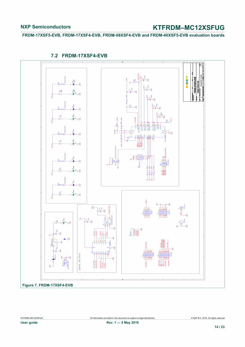
7.2 FRDM-17XSF4-EVB
5 5
4 4
3 3
2 2
1 1
DD
CC
BB
AA
Level Shifter
FRDM
RS
TB
SP
I0_C
SB
CLK
SP
I0_C
LKS
PI0
_MO
SI
SP
I0_M
ISO
CS
NS
_SY
NC
B
CS
NS
OU
T_6
LIM
P
IN1
IN2
IN3
SP
I0_C
SB
1
SP
I0_C
SB
2
OUT_2OUT_4OUT_5OUT_3OUT_1
OU
T_6
SP
I0_C
SB
3S
PI0
_CS
B2
SP
I0_C
SB
1S
PI0
_CS
B0
OU
T_3
OU
T_2
OU
T_1
SP
I0_C
SB
_FR
DM
SP
I0_M
OS
I_F
RD
M
SP
I0_C
LK_F
RD
M
RS
TB
_FR
DM
SP
I0_C
SB
SP
I0_M
OS
I
SP
I0_C
LK
RS
TB
RS
TB
_FR
DM
IN4
CLK
_FR
DM
CLK
_FR
DM
IN2
IN3
IN4
OU
T_5
OU
T_4
OU
T_1
OU
T_2
OU
T_3
OU
T_4
OU
T_5
SP
I0_C
SB
_FR
DM
IN1
CLK
SP
I0_C
SB
0S
PI0
_MO
SI_
FR
DM
SP
I0_M
ISO
_FR
DM
SP
I0_C
SB
3
SP
I0_C
LK_F
RD
M
CS
NS
CS
NS
_SY
NC
B
SP
I0_M
ISO
SP
I0_M
ISO
_FR
DM
AG
ND
AG
ND
AG
ND
AG
ND
AG
ND
AG
ND
AG
ND
AG
ND
AG
ND
AG
ND
5V
AG
ND
AG
ND
AG
ND
AG
ND
AG
ND
AG
ND
AG
ND
AG
ND
AG
ND
AG
ND
AG
ND
AG
ND
AG
ND
AG
ND
AG
ND
AG
ND
AG
ND
AG
ND
AG
ND
AG
ND
AG
ND
AG
ND
AG
ND
AG
ND
VB
AT
VB
AT
VB
AT
VB
AT
5V
5V
5V
5V
5V
P3_
3V
AG
ND
AG
ND
P3_
3V
AG
ND
AG
ND
Dra
win
g T
itle:
Siz
eD
ocum
ent N
umbe
rR
ev
Dat
e:S
heet
of
Pag
e T
itle:
ICA
P C
lass
ifica
tion:
CP
:IU
O:
PU
BI:
SC
H-2
9222
PD
F: S
PF
-292
22F
1
FR
DM
-17X
SF
4-E
VB
C
Frid
ay, M
arch
04,
201
6
FRD
M-1
7XS
F4-E
VB
33
___
___
XD
raw
ing
Titl
e:
Siz
eD
ocum
ent N
umbe
rR
ev
Dat
e:S
heet
of
Pag
e T
itle:
ICA
P C
lass
ifica
tion:
CP
:IU
O:
PU
BI:
SC
H-2
9222
PD
F: S
PF
-292
22F
1
FR
DM
-17X
SF
4-E
VB
C
Frid
ay, M
arch
04,
201
6
FRD
M-1
7XS
F4-E
VB
33
___
___
XD
raw
ing
Titl
e:
Siz
eD
ocum
ent N
umbe
rR
ev
Dat
e:S
heet
of
Pag
e T
itle:
ICA
P C
lass
ifica
tion:
CP
:IU
O:
PU
BI:
SC
H-2
9222
PD
F: S
PF
-292
22F
1
FR
DM
-17X
SF
4-E
VB
C
Frid
ay, M
arch
04,
201
6
FRD
M-1
7XS
F4-E
VB
33
___
___
X
R6
10.0
KD
NP
D9
GR
EE
N
A C
SH
5
SO
LDE
R S
HO
RT
U2
MC
17X
SF
400E
K
CS
3
SC
LK4
SI
5
SO
7
OU
T6
8
VPWR33
IN2
28
RS
T2
OU
T4_
314
LIM
P31
CLK
32
NC
216
NC
317
NC
418
OU
T3_
119
OU
T3_
220
OU
T3_
321
VCC6
GND19
OU
T4_
213
OU
T4_
112
OU
T2_
211
OU
T2_
110
IN4
30IN
329
CP
1
OU
T1_
122
OU
T1_
223
GND224
CS
NS
25
CS
NS
_SY
NC
26
NC
115
IN1
27
D12
GR
EE
ND
NP
A C
C15
0.1U
F
SW
3LI
GH
T T
OU
CH
PU
SH
BU
TT
ON
14
23
C6
0.01
UF
C7
0.02
2UF
J6 CO
N_2
X6
12
34 6
5 78
910
1112
SW
1S
W_D
IP-4
/SM
1234
8765
SH
4
SO
LDE
R S
HO
RT
R13
10.0
K
J4 CO
N_2
X8
12
34 6
5 78
910
1112
1314
1516
D11
GR
EE
N
A C
D7
GR
EE
N
A C
C8
0.02
2UF
R3
10.0
K
C12
0.1U
F
C9
0.02
2UF
R1
220
C10
0.02
2UF
HE
F40
50B
T
U3
1A3
1Y2
2A5
2Y4
3A7
3Y6
4A9
4Y10
5A11
5Y12
6A14
6Y15
NC
113
NC
216
VDD1
VSS8
R10
5.0K
C11
0.02
2UF
DN
P
R7
10.0
K
VC
C
GN
D
U4
74LV
C1G
125G
W-Q
100
1 2 345
J7 CO
N_1
X6
123456
J8
DC
_PO
WE
R_J
AC
K
1 32
R5
10.0
K
J1 CO
N_1
X2
1 2
D6
1N40
02D
NP
AC
J3 CO
N_2
X10
12
34 6
5 78
910
1112
1314
1516
1718
1920
J5 CO
N_2
X8
12
34 6
5 78
910
1112
1314
1516
D5
1N40
02
AC
R9
10.0
K
D4
1N40
02
AC
R12
10.0
K
TP
1
D3
1N40
02
AC
C14
0.1U
F
R14
10.0
K
C5
0.1U
F
D2
1N40
02
AC
R2
10.0
K
C4
0.1U
F
C3 10
uF
U1
LP29
50A
CD
T-5
.0G
OU
T3
IN1
GND4
C2
10uF
SH
3
SO
LDE
R S
HO
RT
D1
CM
MR
1U-0
2
AC
R4
10.0
K
J2 PLU
G_1
X2
1 2
C1
10uF
SW
2
SW
_DIP
-4/S
M1234
8765
R11
1K
D10
GR
EE
N
A C
SH
2
SO
LDE
R S
HO
RT
SH
1
SO
LDE
R S
HO
RT
D8
GR
EE
N
A C
R8
3K
Figure 7. FRDM-17XSF4-EVB

NXP Semiconductors KTFRDM–MC12XSFUGFRDM-17XSF5-EVB, FRDM-17XSF4-EVB, FRDM-08XSF4-EVB and FRDM-40XSF5-EVB evaluation boards
KTFRDM–MC12XSFUG All information provided in this document is subject to legal disclaimers. © NXP B.V. 2016. All rights reserved
User guide Rev. 1 — 5 May 201615 / 23
7.3 FRDM-08XSF4-EVB
5 5
4 4
3 3
2 2
1 1
DD
CC
BB
AA
Level Shifter
FRDM
RS
TB
SP
I0_C
SB
CLK
SP
I0_C
LKS
PI0
_MO
SI
SP
I0_M
ISO
CS
NS
_SY
NC
B
CS
NS
OU
T_6
LIM
P
IN1
IN2
IN3
SP
I0_C
SB
1
SP
I0_C
SB
2
OUT_2OUT_4OUT_5OUT_3OUT_1
OU
T_6
SP
I0_C
SB
3S
PI0
_CS
B2
SP
I0_C
SB
1S
PI0
_CS
B0
OU
T_3
OU
T_2
OU
T_1
SP
I0_C
SB
_FR
DM
SP
I0_M
OS
I_F
RD
M
SP
I0_C
LK_F
RD
M
RS
TB
_FR
DM
SP
I0_C
SB
SP
I0_M
OS
I
SP
I0_C
LK
RS
TB
RS
TB
_FR
DM
IN4
CLK
_FR
DM
CLK
_FR
DM
IN2
IN3
IN4
OU
T_5
OU
T_4
OU
T_1
OU
T_2
OU
T_3
OU
T_4
OU
T_5
SP
I0_C
SB
_FR
DM
IN1
CLK
SP
I0_C
SB
0S
PI0
_MO
SI_
FR
DM
SP
I0_M
ISO
_FR
DM
SP
I0_C
SB
3
SP
I0_C
LK_F
RD
M
CS
NS
CS
NS
_SY
NC
B
SP
I0_M
ISO
SP
I0_M
ISO
_FR
DM
AG
ND
AG
ND
AG
ND
AG
ND
AG
ND
AG
ND
AG
ND
AG
ND
AG
ND
AG
ND
5V
AG
ND
AG
ND
AG
ND
AG
ND
AG
ND
AG
ND
AG
ND
AG
ND
AG
ND
AG
ND
AG
ND
AG
ND
AG
ND
AG
ND
AG
ND
AG
ND
AG
ND
AG
ND
AG
ND
AG
ND
AG
ND
AG
ND
AG
ND
AG
ND
VB
AT
VB
AT
VB
AT
VB
AT
5V
5V
5V
5V
5V
P3_
3V
AG
ND
AG
ND
P3_
3V
AG
ND
AG
ND
Dra
win
g T
itle:
Siz
eD
ocum
ent N
umbe
rR
ev
Dat
e:S
heet
of
Pag
e T
itle:
ICA
P C
lass
ifica
tion:
CP
:IU
O:
PU
BI:
SC
H-2
9224
PD
F: S
PF
-292
24F
1
FR
DM
-08X
SF
4-E
VB
C
Frid
ay, M
arch
04,
201
6
FRD
M-0
8XS
F4-E
VB
33
___
___
XD
raw
ing
Titl
e:
Siz
eD
ocum
ent N
umbe
rR
ev
Dat
e:S
heet
of
Pag
e T
itle:
ICA
P C
lass
ifica
tion:
CP
:IU
O:
PU
BI:
SC
H-2
9224
PD
F: S
PF
-292
24F
1
FR
DM
-08X
SF
4-E
VB
C
Frid
ay, M
arch
04,
201
6
FRD
M-0
8XS
F4-E
VB
33
___
___
XD
raw
ing
Titl
e:
Siz
eD
ocum
ent N
umbe
rR
ev
Dat
e:S
heet
of
Pag
e T
itle:
ICA
P C
lass
ifica
tion:
CP
:IU
O:
PU
BI:
SC
H-2
9224
PD
F: S
PF
-292
24F
1
FR
DM
-08X
SF
4-E
VB
C
Frid
ay, M
arch
04,
201
6
FRD
M-0
8XS
F4-E
VB
33
___
___
X
R6
10.0
KD
NP
D9
GR
EE
N
A C
SH
5
SO
LDE
R S
HO
RT
D12
GR
EE
ND
NP
A C
C15
0.1U
F
SW
3LI
GH
T T
OU
CH
PU
SH
BU
TT
ON
14
23
C6
0.01
UF
U2
MC
08X
SF
421E
KCS
3
SC
LK4
SI
5
SO
7
OU
T6
8
VPWR33
IN2
28
RS
T2
OU
T4_
314
LIM
P31
CLK
32
NC
216
NC
317
NC
418
OU
T3_
119
OU
T3_
220
OU
T3_
321
VCC6
GND19
OU
T4_
213
OU
T4_
112
OU
T2_
211
OU
T2_
110
IN4
30IN
329
CP
1
OU
T1_
122
OU
T1_
223
GND224
CS
NS
25
CS
NS
_SY
NC
26
NC
115
IN1
27
C7
0.02
2UF
J6 CO
N_2
X6
12
34 6
5 78
910
1112
SW
1S
W_D
IP-4
/SM
1234
8765
SH
4
SO
LDE
R S
HO
RT
R13
10.0
K
J4 CO
N_2
X8
12
34 6
5 78
910
1112
1314
1516
D11
GR
EE
N
A C
D7
GR
EE
N
A C
C8
0.02
2UF
R3
10.0
K
C12
0.1U
F
C9
0.02
2UF
R1
220
C10
0.02
2UF
R8
3K
HE
F40
50B
T
U3
1A3
1Y2
2A5
2Y4
3A7
3Y6
4A9
4Y10
5A11
5Y12
6A14
6Y15
NC
113
NC
216
VDD1
VSS8
R10
5.0K
C11
0.02
2UF
DN
P
R7
10.0
K
VC
C
GN
D
U4
74LV
C1G
125G
W-Q
100
1 2 345
J7 CO
N_1
X6
123456
J8
DC
_PO
WE
R_J
AC
K
1 32
R5
10.0
K
J1 CO
N_1
X2
1 2
D6
1N40
02D
NP
AC
J3 CO
N_2
X10
12
34 6
5 78
910
1112
1314
1516
1718
1920
J5 CO
N_2
X8
12
34 6
5 78
910
1112
1314
1516
D5
1N40
02
AC
R9
10.0
K
D4
1N40
02
AC
R12
10.0
K
TP
1
D3
1N40
02
AC
C14
0.1U
F
R14
10.0
K
C5
0.1U
F
D2
1N40
02
AC
R2
10.0
K
C4
0.1U
F
C3 10
uF
U1
LP29
50A
CD
T-5
.0G
OU
T3
IN1
GND4
C2
10uF
SH
3
SO
LDE
R S
HO
RT
D1
CM
MR
1U-0
2
AC
R4
10.0
K
J2 PLU
G_1
X2
1 2
C1
10uF
SW
2
SW
_DIP
-4/S
M1234
8765R
111K
D10
GR
EE
N
A C
SH
2
SO
LDE
R S
HO
RT
SH
1
SO
LDE
R S
HO
RT
D8
GR
EE
N
A C
Figure 8. FRDM-08XSF4-EVB

NXP Semiconductors KTFRDM–MC12XSFUGFRDM-17XSF5-EVB, FRDM-17XSF4-EVB, FRDM-08XSF4-EVB and FRDM-40XSF5-EVB evaluation boards
KTFRDM–MC12XSFUG All information provided in this document is subject to legal disclaimers. © NXP B.V. 2016. All rights reserved
User guide Rev. 1 — 5 May 201616 / 23
7.4 FRDM-40XSF5-EVB
5 5
4 4
3 3
2 2
1 1
DD
CC
BB
AA
Level Shifter
FRDM
RS
TB
SP
I0_C
SB
CLK
SP
I0_C
LKS
PI0
_MO
SI
SP
I0_M
ISO
CS
NS
_SY
NC
B
CS
NS
OU
T_6
LIM
P
IN1
IN2
IN3
SP
I0_C
SB
1
SP
I0_C
SB
2
OUT_2OUT_4OUT_5OUT_3OUT_1
OU
T_6
SP
I0_C
SB
3S
PI0
_CS
B2
SP
I0_C
SB
1S
PI0
_CS
B0
OU
T_3
OU
T_2
OU
T_1
SP
I0_C
SB
_FR
DM
SP
I0_M
OS
I_F
RD
M
SP
I0_C
LK_F
RD
M
RS
TB
_FR
DM
SP
I0_C
SB
SP
I0_M
OS
I
SP
I0_C
LK
RS
TB
RS
TB
_FR
DM
IN4
CLK
_FR
DM
CLK
_FR
DM
IN2
IN3
IN4
OU
T_5
OU
T_4
OU
T_1
OU
T_2
OU
T_3
OU
T_4
OU
T_5
SP
I0_C
SB
_FR
DM
IN1
CLK
SP
I0_C
SB
0S
PI0
_MO
SI_
FR
DM
SP
I0_M
ISO
_FR
DM
SP
I0_C
SB
3
SP
I0_C
LK_F
RD
M
CS
NS
CS
NS
_SY
NC
B
SP
I0_M
ISO
SP
I0_M
ISO
_FR
DM
AG
ND
AG
ND
AG
ND
AG
ND
AG
ND
AG
ND
AG
ND
AG
ND
AG
ND
AG
ND
5V
AG
ND
AG
ND
AG
ND
AG
ND
AG
ND
AG
ND
AG
ND
AG
ND
AG
ND
AG
ND
AG
ND
AG
ND
AG
ND
AG
ND
AG
ND
AG
ND
AG
ND
AG
ND
AG
ND
AG
ND
AG
ND
AG
ND
AG
ND
AG
ND
VB
AT
VB
AT
VB
AT
VB
AT
5V
5V
5V
5V
5V
P3_
3V
AG
ND
AG
ND
P3_
3V
AG
ND
AG
ND
Dra
win
g T
itle:
Siz
eD
ocum
ent N
umbe
rR
ev
Dat
e:S
heet
of
Pag
e T
itle:
ICA
P C
lass
ifica
tion:
CP
:IU
O:
PU
BI:
SC
H-2
9221
PD
F: S
PF
-292
21F
1
FR
DM
-40X
SF
5-E
VB
C
Frid
ay, M
arch
04,
201
6
FRD
M-4
0XS
F5-E
VB
33
___
___
XD
raw
ing
Titl
e:
Siz
eD
ocum
ent N
umbe
rR
ev
Dat
e:S
heet
of
Pag
e T
itle:
ICA
P C
lass
ifica
tion:
CP
:IU
O:
PU
BI:
SC
H-2
9221
PD
F: S
PF
-292
21F
1
FR
DM
-40X
SF
5-E
VB
C
Frid
ay, M
arch
04,
201
6
FRD
M-4
0XS
F5-E
VB
33
___
___
XD
raw
ing
Titl
e:
Siz
eD
ocum
ent N
umbe
rR
ev
Dat
e:S
heet
of
Pag
e T
itle:
ICA
P C
lass
ifica
tion:
CP
:IU
O:
PU
BI:
SC
H-2
9221
PD
F: S
PF
-292
21F
1
FR
DM
-40X
SF
5-E
VB
C
Frid
ay, M
arch
04,
201
6
FRD
M-4
0XS
F5-E
VB
33
___
___
X
SH
5
SO
LDE
R S
HO
RT
D9
GR
EE
N
A C
R6
10.0
K
D12
GR
EE
N
A C
C6
0.01
UF
SW
3LI
GH
T T
OU
CH
PU
SH
BU
TT
ON
14
23
C15
0.1U
F
J4 CO
N_2
X8
12
34 6
5 78
910
1112
1314
1516
R13
10.0
K
SH
4
SO
LDE
R S
HO
RT
SW
1S
W_D
IP-4
/SM
1234
8765
J6 CO
N_2
X6
12
34 6
5 78
910
1112
C7
0.02
2UF
C8
0.02
2UF
D7
GR
EE
N
A C
D11
GR
EE
N
A C
C9
0.02
2UF
C12
0.1U
F
R3
10.0
K
C10
0.02
2UF
R1
220
C11
0.02
2UF
R10
5.0K
HE
F40
50B
T
U3
1A3
1Y2
2A5
2Y4
3A7
3Y6
4A9
4Y10
5A11
5Y12
6A14
6Y15
NC
113
NC
216
VDD1
VSS8
R5
10.0
K
J8
DC
_PO
WE
R_J
AC
K
1 32
J7 CO
N_1
X6
123456
VC
C
GN
D
U4
74LV
C1G
125G
W-Q
100
1 2 345
R7
10.0
K
J3 CO
N_2
X10
12
34 6
5 78
910
1112
1314
1516
1718
1920
D6
1N40
02
AC
J1 CO
N_1
X2
1 2
R8
3K
D5
1N40
02
AC
J5 CO
N_2
X8
12
34 6
5 78
910
1112
1314
1516
TP
1
R12
10.0
K
D4
1N40
02
AC
R9
10.0
K
C5
0.1U
F
R14
10.0
K
C14
0.1U
F
D3
1N40
02
AC
C3 10
uF
C4
0.1U
F
R2
10.0
K
D2
1N40
02
AC
U2
MC
40X
SF
500E
K
CS
3
SC
LK4
SI
5
SO
7
OU
T6
8
VPWR33
IN2
28
RS
T2
OU
T4_
314
LIM
P31
CLK
32
NC
216
OU
T5_
117
OU
T5_
218
OU
T3_
119
OU
T3_
220
OU
T3_
321
VCC6
GND19
OU
T4_
213
OU
T4_
112
OU
T2_
211
OU
T2_
110
IN4
30IN
329
CP
1
OU
T1_
122
OU
T1_
223
GND224
CS
NS
25
CS
NS
_SY
NC
26
NC
115
IN1
27
R4
10.0
K
D1
CM
MR
1U-0
2
AC
SH
3
SO
LDE
R S
HO
RT
C2
10uF
U1
LP29
50A
CD
T-5
.0G
OU
T3
IN1
GND4
D10
GR
EE
N
A C
R11
1K
SW
2
SW
_DIP
-4/S
M1234
8765
C1
10uF
J2 PLU
G_1
X2
1 2
D8
GR
EE
N
A C
SH
1
SO
LDE
R S
HO
RT
SH
2
SO
LDE
R S
HO
RT
Figure 9. FRDM-40XSF5-EVB

NXP Semiconductors KTFRDM–MC12XSFUGFRDM-17XSF5-EVB, FRDM-17XSF4-EVB, FRDM-08XSF4-EVB and FRDM-40XSF5-EVB evaluation boards
KTFRDM–MC12XSFUG All information provided in this document is subject to legal disclaimers. © NXP B.V. 2016. All rights reserved
User guide Rev. 1 — 5 May 201617 / 23
8 Board layout
Figure 10. Top layout

NXP Semiconductors KTFRDM–MC12XSFUGFRDM-17XSF5-EVB, FRDM-17XSF4-EVB, FRDM-08XSF4-EVB and FRDM-40XSF5-EVB evaluation boards
KTFRDM–MC12XSFUG All information provided in this document is subject to legal disclaimers. © NXP B.V. 2016. All rights reserved
User guide Rev. 1 — 5 May 201618 / 23
Figure 11. Bottom layout

NXP Semiconductors KTFRDM–MC12XSFUGFRDM-17XSF5-EVB, FRDM-17XSF4-EVB, FRDM-08XSF4-EVB and FRDM-40XSF5-EVB evaluation boards
KTFRDM–MC12XSFUG All information provided in this document is subject to legal disclaimers. © NXP B.V. 2016. All rights reserved
User guide Rev. 1 — 5 May 201619 / 23
9 Bill of Materials
Bill of materials for FRDM-17XSF5-EVB, FRDM-17XSF4-EVB, FRDM-08XSF4-EVB andFRDM-40XSF5-EVB are available in the Download section of the FRDM-MC12XSF ToolSummary page at the following url: http://www.nxp.com/FRDM-MC12XSF.
10 References
Following are URLs where you can obtain information on related NXP products andapplication solutions:
NXP.com support pages Description URLFreedom development boards Freedom development platform http://www.nxp.com/freedom
Freedom evaluation board Freedom evaluation board for eXtremeswitch 12XSF family
http://www.nxp.com/FRDM-MC12XSF
FRDM-KL25Z Freedom development platform forKinetis KL14, KL15, KL24, KL25 MCUs
http://www.nxp.com/FRDM-KL25Z
SPIGen SPI generator software http://www.nxp.com/SPIGEN
Kinetis Design Studio Integrated development environmentwith Processor Expert
http://www.nxp.com/KDS
11 Revision history
Revision Date Description of changes1.0 5/2016 Initial release
12 Contact information
Visit http://www.nxp.com/support for a list of phone numbers within your region.Visit http://www.nxp.com/warranty to submit a request for tool warranty.

NXP Semiconductors KTFRDM–MC12XSFUGFRDM-17XSF5-EVB, FRDM-17XSF4-EVB, FRDM-08XSF4-EVB and FRDM-40XSF5-EVB evaluation boards
KTFRDM–MC12XSFUG All information provided in this document is subject to legal disclaimers. © NXP B.V. 2016. All rights reserved
User guide Rev. 1 — 5 May 201620 / 23
13 Legal information
13.1 DefinitionsDraft — The document is a draft version only. The content is still underinternal review and subject to formal approval, which may result inmodifications or additions. NXP Semiconductors does not give anyrepresentations or warranties as to the accuracy or completeness ofinformation included herein and shall have no liability for the consequencesof use of such information.
13.2 DisclaimersInformation in this document is provided solely to enable system andsoftware implementers to use NXP products. There are no express orimplied copyright licenses granted hereunder to design or fabricate anyintegrated circuits based on the information in this document. NXP reservesthe right to make changes without further notice to any products herein.
NXP makes no warranty, representation, or guarantee regarding thesuitability of its products for any particular purpose, nor does NXP assumeany liability arising out of the application or use of any product or circuit,and specifically disclaims any and all liability, including without limitationconsequential or incidental damages. “Typical” parameters that may be
provided in NXP data sheets and/ or specifications can and do vary indifferent applications, and actual performance may vary over time. Alloperating parameters, including “typicals,” must be validated for eachcustomer application by customer's technical experts. NXP does notconvey any license under its patent rights nor the rights of others. NXP sellsproducts pursuant to standard terms and conditions of sale, which can befound at the following address: nxp.com/salestermsandconditions.
13.3 TrademarksNotice: All referenced brands, product names, service names andtrademarks are the property of their respective owners.
NXP — is a trademark of NXP B.V.the NXP logo — is a trademark of NXP B.V.Freescale — is a trademark of NXP B.V.the Freescale logo — is a trademark of NXP B.V.CodeWarrior — is a trademark of NXP B.V.Kinetis — is a trademark of NXP B.V.Processor Expert — is a trademark of NXP B.V.SMARTMOS — is a trademark of NXP B.V.

NXP Semiconductors KTFRDM–MC12XSFUGFRDM-17XSF5-EVB, FRDM-17XSF4-EVB, FRDM-08XSF4-EVB and FRDM-40XSF5-EVB evaluation boards
KTFRDM–MC12XSFUG All information provided in this document is subject to legal disclaimers. © NXP B.V. 2016. All rights reserved
User guide Rev. 1 — 5 May 201621 / 23
TablesTab. 1. Device features ................................................. 5Tab. 2. Freedom board overview .................................. 6Tab. 3. LED description .................................................7Tab. 4. Connectors description ......................................7
Tab. 5. Switches definition ............................................ 8Tab. 6. Test point definition ...........................................8Tab. 7. Compatibility with selected MCU Freedom
boards ............................................................... 8
NXP Semiconductors KTFRDM–MC12XSFUGFRDM-17XSF5-EVB, FRDM-17XSF4-EVB, FRDM-08XSF4-EVB and FRDM-40XSF5-EVB evaluation boards
KTFRDM–MC12XSFUG All information provided in this document is subject to legal disclaimers. © NXP B.V. 2016. All rights reserved
User guide Rev. 1 — 5 May 201622 / 23
FiguresFig. 1. Freedom platform – MCU Freedom board
with analog Freedom shield .............................. 4Fig. 2. Freedom board overview (without load) ............ 6Fig. 3. SPIGen GUI .................................................... 10Fig. 4. Hardware setup ...............................................11Fig. 5. FRDM-KL25Z connected .................................12
Fig. 6. FRDM-17XSF5-EVB ........................................13Fig. 7. FRDM-17XSF4-EVB ........................................14Fig. 8. FRDM-08XSF4-EVB ........................................15Fig. 9. FRDM-40XSF5-EVB ........................................16Fig. 10. Top layout ....................................................... 17Fig. 11. Bottom layout .................................................. 18

NXP Semiconductors KTFRDM–MC12XSFUGFRDM-17XSF5-EVB, FRDM-17XSF4-EVB, FRDM-08XSF4-EVB and FRDM-40XSF5-EVB evaluation boards
Contents1 FRDM-17XSF5-EVB ............................................. 12 Important notice ..................................................23 Getting started .................................................... 33.1 Kit contents/packing list ..................................... 33.2 Jump start ..........................................................33.3 Required equipment .......................................... 33.4 System requirements .........................................44 Understanding the Freedom platform ............... 45 Getting to know the hardware ........................... 55.1 Board overview ..................................................55.2 Device features ..................................................55.3 Board description ...............................................65.3.1 LEDs .................................................................. 75.3.2 Connectors .........................................................75.3.3 Switches definition .............................................85.3.4 Test point definition ........................................... 85.3.5 Freedom board headers .................................... 86 Installing the software and setting up the
hardware .............................................................. 96.1 Using SPIGen software ..................................... 96.1.1 Installing SPIGen freeware on your
computer ............................................................96.1.2 Connecting FRDM-KL25Z Freedom
Development Platform ..................................... 106.1.3 Setting up the hardware using SPIGen ............116.1.4 Running the example batch files ..................... 126.2 Using Kinetis Design Studio and Processor
Expert ...............................................................127 Schematics ........................................................ 137.1 FRDM-17XSF5-EVB ........................................ 137.2 FRDM-17XSF4-EVB ........................................ 147.3 FRDM-08XSF4-EVB ........................................ 157.4 FRDM-40XSF5-EVB ........................................ 168 Board layout ...................................................... 179 Bill of Materials ................................................. 1910 References ......................................................... 1911 Revision history ................................................ 1912 Contact information .......................................... 1913 Legal information ..............................................20
© NXP B.V. 2016. All rights reservedFor more information, please visit: http://www.nxp.comFor sales office addresses, please send an email to: [email protected] on 5 May 2016