koki s3x58-m406-3 lead free solder paste - adtool s3x48-m406-3.pdf · anti-pillow defect lead free...
TRANSCRIPT
Anti-Pillow Defect LLeeaadd FFrreeee Solder Paste S3X48-M406-3
PREVENTS the occurrence of HIDDEN PILLOW DEFECT and ensures the quality of solder joints.
Ensures OUTSTANDING continual PRINTABILITY with super fine pitch and CSP applications and has long stencil idle time. Heat RESISTANT new flux formula achieves complete solder melting and wetting on micro-components and footprints.
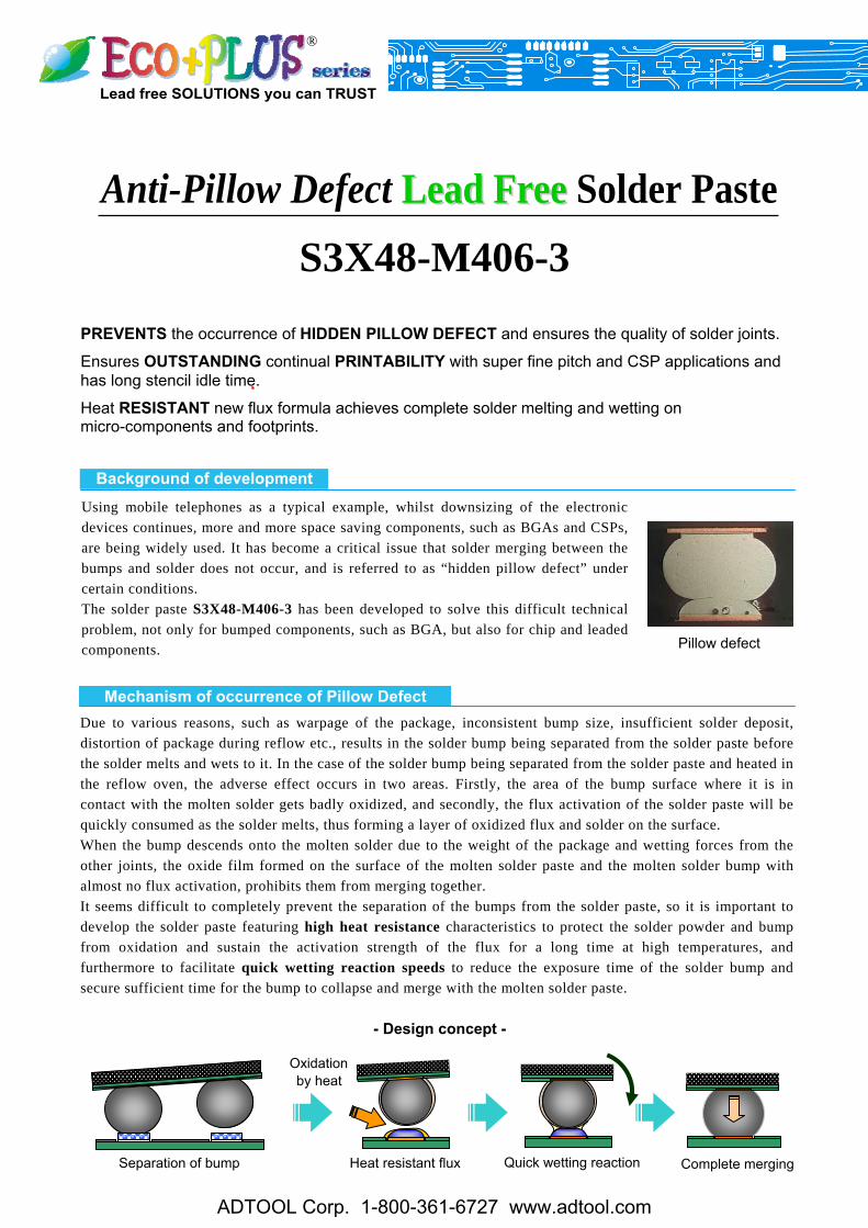
Using mobile telephones as a typical example, whilst downsizing of the electronic devices continues, more and more space saving components, such as BGAs and CSPs, are being widely used. It has become a critical issue that solder merging between the bumps and solder does not occur, and is referred to as “hidden pillow defect” under certain conditions. The solder paste S3X48-M406-3 has been developed to solve this difficult technical problem, not only for bumped components, such as BGA, but also for chip and leaded components. Due to various reasons, such as warpage of the package, inconsistent bump size, insufficient solder deposit, distortion of package during reflow etc., results in the solder bump being separated from the solder paste before the solder melts and wets to it. In the case of the solder bump being separated from the solder paste and heated in the reflow oven, the adverse effect occurs in two areas. Firstly, the area of the bump surface where it is in contact with the molten solder gets badly oxidized, and secondly, the flux activation of the solder paste will be quickly consumed as the solder melts, thus forming a layer of oxidized flux and solder on the surface. When the bump descends onto the molten solder due to the weight of the package and wetting forces from the other joints, the oxide film formed on the surface of the molten solder paste and the molten solder bump with almost no flux activation, prohibits them from merging together. It seems difficult to completely prevent the separation of the bumps from the solder paste, so it is important to develop the solder paste featuring high heat resistance characteristics to protect the solder powder and bump from oxidation and sustain the activation strength of the flux for a long time at high temperatures, and furthermore to facilitate quick wetting reaction speeds to reduce the exposure time of the solder bump and secure sufficient time for the bump to collapse and merge with the molten solder paste.
Lead free SOLUTIONS you can TRUST
®
Background of development
Mechanism of occurrence of Pillow Defect
Oxidation by heat
Separation of bump Heat resistant flux Quick wetting reaction Complete merging
Pillow defect
- Design concept -
ADTOOL Corp. 1-800-361-6727 www.adtool.com

A variety of optimizations on the flux formula has been implemented to significantly enhance the heat resistance even at high pre-heat conditions (200ºC), such as the selection of anti-oxidant additives and the prevention of flux bleed from the solder deposit to further protect the solder particles. ► Melting of super fine pattern
► Retention of flux activation Observe influence of progressive oxidation of flux/molten solder over retention of flux activation.
Wetting reaction speed has been enhanced by controlling the flow behavior during the heating process by the adoption of heat resistant flux formulations. In the wetting test, the chip capacitor was placed on once reflowed solder and reflowed again to simulate the pillow phenomenon. S3X48-M406-3 started to wet to the component at 224ºC, whilst the conventional paste started at 228ºC. Such a quicker wetting action will help to allow sufficient time for the bump to merge completely with the solder.
Improvement of heat resistance
• Stencil : 0.12mm thickness, 100% aperture to pad • Pad : 0.35mm dia. BGA pattern • Reflow profile :
50 100 150 200 250
0 100 200 300 Time (sec.)
200ºC x 100sec.
Tem
pera
ture
(ºC
)
• Stencil : 0.12mm thickness, 100% aperture to pad size • Pad : 0.8 x 0.8mm chip pad • Solder ball : Sn3Ag0.5Cu, 0.76mm diameter • Test procedure : Melt solder paste on hot plate and drop solder ball at every 20sec.
Enhancement of wetting reaction speed
Conventional product
0.35mm diameter pattern
S3X48-M406-3
300
Solder PCB
Hot plate
Solder ball
Immediate after melting
20 sec. after melting
40 sec. after melting
60 sec. aftermelting
Complete merging Complete merging Complete merging Partial merging
S3X48- M406-3
Conventional paste
Complete merging No mergingPartial merging Partial merging
• Stencil : 0.12mm thickness, • Preconditioning of component: 150ºC for 3 hours baking
Reflow solder Reflow again with component
S3X48- M406-3
Conventional paste
222ºC 224ºC 226ºC 228ºC
ADTOOL Corp. 1-800-361-6727 www.adtool.com

Significant enhancements in the heat resistance of the flux and wetting reaction speed have succeeded in reducing the occurrence of hidden pillow defect. S3X48-M406-3 assures robust wetting action to BGA bumps with intentional extra oxidation. ► Pillow defect test
New formula S3X48-M406-3 wets much faster than the conventional product and immediately breaks the oxide film formed on the surface of both the solder bump and the molten solder and enables quicker wetting and complete collapse of the bump to secure joint quality.
► Observation of pillow defect
S3X48-M406-3, new heat resistant and enhanced wetting reaction speed formula, exhibited drastic reduction of pillow defects.
• Material : Glass epoxy FR-4 • Surface treatment : OSP • Stencil thickness : 0.12mm • Stencil aperture : 100% aperture opening to pad • Pad size : 0.5mm • Atmosphere : Air • Component (BGA): SnAgCu, 1.0mm pitch, 196 bumps x 5, pre-conditioned at 180ºC×100sec. • Procedure: 1. Reflow solder paste without BGA. 2. Place BGA on pre-reflowed solder. 3. Reflow it.
Cross-section
Complete merging
Pillow defect Incompletecollapse
IInniittiiaall 222200ººCC 223300ººCC 224400 ººCC
S3X48- M406-3
Conventional paste
Pillow defect Incomplete collapse Complete merging
After peel-off
S3X48-M406-3
Conventional paste
PCB side BGA side
- Pry result -
5.79.7
30.1
60.2
0.4
93.9
0
20
40
60
80
100
Complete merging Incompletecollapse
Pillow defect
Rat
e (%
)
S3X48-M406-3Conventional paste
Wetting performance with BGA
ADTOOL Corp. 1-800-361-6727 www.adtool.com
32-1, Senju Asahi-cho, Adachi-ku, Tokyo 120-0026 Tel : (03) 5244-1521 Fax : (03) 5244-1525 www.ko-ki.co.jp
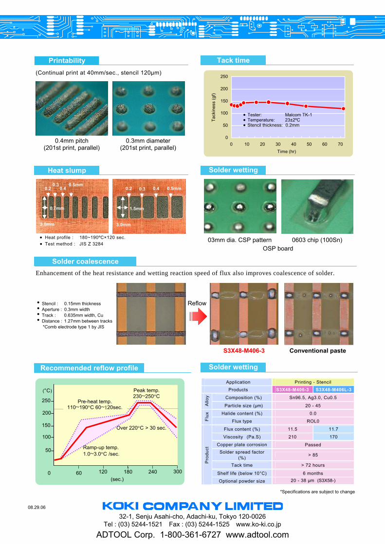
(Continual print at 40mm/sec., stencil 120μm)
Enhancement of the heat resistance and wetting reaction speed of flux also improves coalescence of solder.
Application Printing - Stencil
Products S3X48-M406-3 S3X48-M406L-3
Composition (%) Sn96.5, Ag3.0, Cu0.5
Allo
y
Particle size (μm) 20 - 45
Halide content (%) 0.0
Flux
Flux type ROL0
Flux content (%) 11.5 11.7
Viscosity (Pa.S) 210 170
Copper plate corrosion Passed Solder spread factor
(%) > 85
Tack time > 72 hours
Shelf life (below 10°C) 6 months
Pro
duct
Optional powder size 20 - 38 μm (S3X58-)
Printability Tack time
0.4mm pitch (201st print, parallel)
0.3mm diameter (201st print, parallel)
0
50
100
150
200
250
0 10 20 30 40 50 60 70Time (hr)
Tack
ines
s (g
f)
• Tester: Malcom TK-1 • Temperature: 23±2ºC • Stencil thickness: 0.2mm
• Heat profile : 180~190ºC×120 sec. • Test method : JIS Z 3284
Heat slump Solder wetting
0.2 0.3
0.4
0.7mm
0.5mm
3.0mm
0.3 0.5mm 0.2 0.4
1.5mm
3.0mm
03mm dia. CSP pattern 0603 chip (100Sn) OSP board
Solder coalescence
Recommended reflow profile Solder wetting
08.29.06
• Stencil : 0.15mm thickness • Aperture : 0.3mm width • Track : 0.635mm width, Cu • Distance : 1.27mm between tracks *Comb electrode type 1 by JIS
Reflow
S3X48-M406-3 Conventional paste
*Specifications are subject to change
Pre-heat temp. 110~190°C 60~120sec.
Peak temp. 230~250°C
(°C)
50
100
150
200
250
Ramp-up temp. 1.0~3.0°C /sec.
120 60 180 240 300 (sec.)
Over 220°C > 30 sec.
0
ADTOOL Corp. 1-800-361-6727 www.adtool.com