kochi university of technology academic resource...
TRANSCRIPT

Kochi University of Technology Academic Resource Repository
�
Title
A study of degradation mechanism of In-Ga-Zn-O t
hin-film transistor under negative bias-illumina
tion stress and positive bias stress for highly
reliable display devices.
Author(s) MAI, Phi Hung
Citation 高知工科大学, 博士論文.
Date of issue 2015-09
URL http://hdl.handle.net/10173/1324
Rights
Text version ETD
�
�
Kochi, JAPAN
http://kutarr.lib.kochi-tech.ac.jp/dspace/

Kochi University of Technology
Department of Environmental Science and Engineering
Kochi, Japan
A Study of Degradation Mechanism of In-Ga-Zn-O
Thin-Film Transistor under Negative Bias-Illumination Stress
and Positive Bias Stress for Highly Reliable Display Devices
Ph.D candidate: Mai Phi Hung
Supervisor: Prof. Mamoru Furuta
A dissertation submitted to Kochi University of Technology
in partial fulfillment of the requirements for
the degree of Doctor of Engineering
September, 2015

Acknowledgements
It is with immense gratitude that I acknowledge the support and help of all those who have been
beside me during my research period and the preparation of this thesis.
Particular thanks are due to my academic supervisor, Prof. Mamoru Furuta, professor of Kochi
University of Technology (KUT), for his insightful advice, continuous encouragement and patient personal
counseling as well as the guidance and commendation he has given me. I would like to thank my co-
advisors Prof. T.Maeda, Prof. L.Chaoyang, A.Prof. S.Momota and A.Prof. Nitta Noriko for their kindly
help.
I wish to express my gratitude and sincere thanks to Dr. Dapeng Wang, assistance professor of KUT,
for teaching me fabrication and evaluation techniques. Your support in both research work and life helped
me a lot. I would also like to thank A.Prof. Kawaharamura Toshiyuki for teaching me XRD, XRR, and
mist CVD, and A.Prof. Nitta Noriko, who introduced me FIB and FE-SEM. I really appreciate Prof.
Hiroshi Furuta ’s help with fitting the XRR data.
I am very grateful to Prof. Lawrence Hunter, who spent a lot of time and effort on editing my papers.
Your academic English writing courses were one of the most effective courses that I have taken in KUT.
I sincerely appreciate Shane-san, Yoshida Motoi-san and Mr. Toda for helping me establishing my
life in Japan. I would like to thank to the M.Furuta lab members for their cooperation and academic
support.
I really appreciate Prof. Kubo, Ms. Mari Yamasaki, Ms. Sakamoto Kimiko, Ms. Miki Okauchi, Ms.
Saki Hamamura and all KUT IRC staff members for helping to make my life in Japan comfortable, and
memorable.
Words cannot express my gratitude to my family for their encouragement and many sacrifices to
ensure I was able to complete the study.
i
A Study of Degradation Mechanism of In-Ga-Zn-O Thin-Film Transistor
under Negative Bias-Illumination Stress and Positive Bias Stress for Highly
Reliable Display Devices
Abstract
In-Ga-Zn-O (IGZO) is an ionic amorphous oxide semiconductor, which has high field effect
mobility (10 ~ 30 cm2/Vs), transparence to visible light (bandgap of ~ 3.2 eV), and room
temperature deposition. These properties make IGZO thin film transistors (TFTs) a promising
candidate for active-matrix backplane of flat panel displays (FPDs). Low power consumption,
high frame rate, and ultra-high resolution are some advantages of FPDs driven by an IGZO TFT
array compared with an amorphous Si TFT. In FPDs, a negative voltage is normally applied to
the gate electrode when the pixel is held. Besides that, TFTs can also be illuminated by back
light unit. Therefore, the TFTs are operated under negative bias and illumination stress (NBIS).
On the other hand, a positive voltage is applied to the gate electrode when TFT is operated at the
on-state. The TFTs are operated under positive bias stress (PBS). Therefore, the reliability of
TFTs under NBIS and under PBS is required for the display application. However, reliability of
IGZO TFT under PBS and under NBIS has been known to be critical issues. This research
focuses on investigating the degradation mechanism of IGZO TFT under PBS and under NBIS.
Based on the investigated degradation mechanism, a method to improve the reliability of IGZO
TFT under PBS and NBIS was proposed. This dissertation includes 8 chapters.
+) Chapter 1 is an overview on the history of display technology and of materials used for
TFTs, which have been used in FPDs backplane. The reasons for high carrier mobility in
amorphous IGZO comparing to that in amorphous silicon will also be explained.
+) Chapter 2 will describe the working principle of the deposition and evaluation equipments
that were used in this research, such as DC-magnetron sputtering, Plasma-Enhanced Chemical
Vapor Deposition (PECVD), X-ray Reflectivity Measurement (XRR), and Secondary Ion Mass
Spectrometry (SIMS) Measurement, and so on.
+) In chapter 3, we will introduce our new measurement method, which we have named as
Positive Gate Pulse Mode (PGPM). PGPM was used to investigate the NBIS degradation

ii
mechanism. Due to the importance of the NBIS reliability issue in FPDs application, a number of
researches relating to the NBIS degradation have been reported. Trapped holes in the gate
insulator (GI), generated defects in the channel have been widely accepted as reasons for the
NBIS instability in IGZO TFT.
In previous reports, TFT transfer characteristic were measured by single sweeping mode
(SSM), in which the gate voltage was swept half cycle, for instance from a negative voltage to a
positive voltage. However, we found that the SSM did not fully capture the NBIS degradation
behaviors. Therefore, Double Sweeping Mode (DSM) was used to measure the transfer
characteristics of IGZO TFT under NBIS. DSM is a transfer characteristic measurement method
in which gate voltage was swept one cycle, for instance from a negative voltage to a positive
voltage and reversed. By using DSM, a new NBIS degradation behavior - a positive shift in
reverse curve - was observed during NBIS stress time. Threshold voltage (Vth) in reverse
measurement (Vrev) shifted positively without subthreshold swing (Ss) degradation. The change
in Vrev with NBIS stress time was well fitted by a stretched-exponential equation. These results
indicate that trapped electrons at the back channel interface are the reason for the positive shift in
reverse curve. By using DSM, a new mechanism for the NBIS instability - the trapped electrons
at the back channel interface - was found.
Using DSM, we also found that TFT hysteresis (Vh) increased with NBIS duration. The
results of our studies indicate that the trapping/detrapping of holes and the
generation/stabilization of defects could be reasons for the increase in hysteresis. Therefore, a
quantitative analysis effect of the trapped holes and the generated defects is necessary for finding
a method to improve the NBIS reliability. In order to do that, we developed a novel measurement
method, which we named Positive Gate Pulse Mode (PGPM). PGPM is a transfer characteristic
measurement method in which a short positive gate pulse is applied to the TFT before every
transfer characteristic measurement. Results measured by PGPM indicate that the hole trapping
in the GI is the main cause of the NBIS instability in the IGZO TFT. The contribution of
hysteresis induced by the trapped holes to the hysteresis was 80%. Therefore, reducing the hole
trapping in the GI will significantly improve the NBIS stability of the IGZO TFT. Based on the
results obtained by DSM and PGPM, a new degradation mechanism of the IGZO TFT under
NBIS was proposed. Quality of the IGZO channel, of the back channel interface and of the GI
iii
strongly affects the NBIS reliability of IGZO TFT. Therefore, the effects of channel film density
and of the back channel quality on the NBIS reliability will be discussed in chapter 4, and 5,
respectively. Chapter 6 will discuss the hole trapping mechanism and a driving method to
improve the NBIS reliability of the IGZO TFT.
+) In chapter 4, the effect of film density of IGZO channel on the defect creation in IGZO
TFT under NBIS was investigated by using PGPM. The IGZO channel was deposited by DC-
magnetron sputtering at a substrate temperature of without heating, 150, 250oC. The film density
of IGZO channel which was measured by X-ray reflectivity (XRR) measurement increased with
deposition temperature. The PGPM was conducted to quantitative analyze the effect of IGZO
deposition temperature on the trapped holes and on the generated defects. Results indicated that
the generated defects in the channel can be reduced by increasing the film density of the IGZO
channel. The positive shift in reversed curve was greater when the film density of the channel
decreased. This result implies that the electron trapping at the back channel interface was
reduced with the IGZO film density. In other words, high film density of the channel can reduce
generation of the defects not only in the channel but also at the back channel interface, resulting
an improvement of the NBIS reliability. However, it was also found that the hole trapping in GI
was not dependent on the IGZO film density.
+) In chapter 5, we investigated the effects of back channel interface quality on the NBIS
reliability. Quality of the back channel interface was varied by the PE-CVD plasma power of
SiOx etching stopper (ES) deposition. The plasma power of SiOx ES deposition was varied as 40,
50 and 55 W. A positive shift in reverse curve and hysteresis induced by generated defects was
smaller when the plasma power decreased. This result implies that the generation of the defects
at the back channel interface and in the channel could be reduced by decreasing the plasma
power of the SiOx ES deposition.
+) Chapter 6: We will present hole generation mechanism and propose a driving method to
improve the NBIS reliability. As reported in chapter 3, the results obtained from PGPM indicated
that hole trapping at the GI/channel interface is the main cause of the NBIS instability in IGZO
TFT. A reduction in the hole trapping at the GI/channel interface should strongly improve the
NBIS reliability. One way to reduce hole trapping is by increasing potential barriers to hole
trapping at the GI/channel interface. However, it is difficult to evaluate the energy barrier for

iv
hole trapping if the effects of trapped holes and generated defects on the NBIS instability were
not separated. Using PGPM to separate this effect, the average effective energy barrier for hole
trapping in GI was calculated to be 0.39 eV. SiOx and AlOx have been found to be the best GI
materials to reduce hole trapping in the GI. Therefore, the hole generation mechanism was
investigated in order to find another method to further reducing the hole trapping in the GI. The
hole generation mechanism was classified by studying the effects of negative duration and of
light intensity on the NBIS degradation behaviors. The obtained results suggest hole generation.
The generated defects are unstable and act as midgap trap states for hole generation. These
results suggest that a reduction of DOS exiting at midgap will improve the NBIS stability. The
results obtained from PGPM suggested that, the midgap trap state could be stabilized by a
positive gate pulse. Therefore, the NBIS stability of the IGZO TFT could be improved by
applying a positive gate pulse alternatively with a negative gate pulse. In other words, in order to
improve the NBIS stability, the FPDs need to be working at high frame rate and low refresh
time.
+) Chapter 7 will covers the PBS degradation mechanism and method to improve the PBS
reliability. PBS reliability of IGZO TFT is not such as serious problem compared with the NBIS
reliability; although the reliability of the IGZO TFT under PBS has gained the attention of many
researchers. The PBS degradation mechanism has been extensively investigated. Trapped
electrons at the GI and deep defects creation in the channel have been widely acknowledged as
reasons for the PBS instability. The deep defect creation in IGZO TFT under PBS has been
predicted by the study of the activation energy of electron trapping into and detrapping from
(recovery process) the GI. However, direct evidence of the deep defect creation and the energy
level of the created defects has not yet been reported. This is due to the fact that, the trapped
electrons and the created deep defects induce the same degradation behavior in both transfer and
C-V characteristic. In this study, the conductance measurement method was used to investigate
the PBS degradation mechanism of the IGZO TFT. The conductance measurement method not
only measures the density of state at the GI/channel interface but also extracts the defect
properties such as capturing cross section and capturing time. This information is important to
recognize the characteristicss of the defects that was overlapped each other. The obtained results
indicate that the stabilization of donor-like interface defects is a reason for the PBS instability.
We also investigate the effects of post annealing time on the PBS stability of the IGZO TFT.

v
Results show that, the PBS stability increased with post annealing time. When the post annealing
time increased from 1 to 5 hours, the electron trapping at the IGZO/SiOx interface was reduced.
This is a reason for the PBS improvement mentioned above. However, when the post annealing
time was increased to 5 hours, deep acceptor-like interface defects were detected. The defects
were located just below Fermi level. This result also suggests that the PBS degradation
mechanism changed from donor-like defects stabilization to deep acceptor-like defects creation.
+) Chapter 8 is conclusions of this thesis. The NBIS degradation mechanism of IGZO TFT
was investigated by using the DSM and PGPM. We clarified that hole trapping in the GI, the
defect generation in the TFT channel and electron trapping at the back channel interface was
reasons for the NBIS instability of the IGZO TFTs. The PGPM, a new measurement method,
was successfully developed to separate the effects of hole trapping and of defect generation on
the NBIS instability. Results obtained from PGPM indicate that hole trapping was the main
cause of the NBIS instability. By separating effects of hole trapping and of defects generation, a
hole trapping energy barrier of 0.39 eV was calculated for the IGZO/SiOx interface. The electron
trapping at the back channel interface and the defect generation in the channel was controlled by
either the film density of the channel or the PE-CVD plasma power of the SiOx ES deposition.
The generated defects were unstable electrons and act as midgap traps for hole generation. The
generated defects could be stabilized by capturing electrons. Based on these results, a control
algorithm of FPDs driving was also proposed to improve the NBIS stability of the IGZO TFT.
An increasing frame rate and reduce refresh time of the FPDs significantly improved the NBIS
stability of the IGZO TFT. Results in chapter 3, 4, 5, 6 indicate that the PGPM is an effective
measurement method for investigating the degradation mechanism. The results of PGPM make a
valuable contribution to the work to improve the NBIS reliability of IGZO.
The PBS degradation mechanism of IGZO TFT was also clarified by the conductance
measurement method. The donor-like interface defects act as the electron trap states and were
stabilized by capturing electrons. The stabilization of donor-like interface defects was the main
reason for the PBS instability in the TFT. An increasing post annealing time reduced electron
trapping in the GI of PE-CVD SiOx. The acceptor-like interface defects were experimentally
detected by the conductance measurement method. The PBS reliability of IGZO TFT can be
improved by increasing the post annealing time.

vi
Table of Contents
Table of Contents ................................................................................................... vi
Figure captions ........................................................................................................................... ix
Chapter 1: Introduction .......................................................................................... 1
1.1 Display technology ........................................................................................................... 1
1.2 Amorphous oxide semiconductor TFTs ................................................................................ 2
1.3 Single component oxide TFTs .............................................................................................. 2
1.4 Multicomponent oxide TFTs ................................................................................................. 3
1.5 Carrier transport and subgap defect in oxide semiconductor. ............................................... 6
1.6 Thesis proposal ...................................................................................................................... 8
Chapter 2: TFT Fabrication and characterization ............................................11
2.1 Thin film deposition and processing ................................................................................... 11
2.1.1 DC magnetron sputtering ............................................................................................. 11
2.1.2 Plasma-enhanced chemical vapor deposition (PE-CVD) ............................................ 12
2.1.3 Inductively coupled plasma chemical vapor deposition (ICP-CVD) ........................... 14
2.1.4 Dry-Etching .................................................................................................................. 15
2.2 Characterization techniques ................................................................................................ 16
2.2.1 Secondary ion mass spectroscopy (SIMS) .................................................................... 16
2.2.2 X-ray diffraction (XRD) and X-ray reflectivity (XRR) .................................................. 17
2.2.3 Initial properties and reliability testing........................................................................ 19
2.2.4 Flat band calculation and Conductance measurement method ................................... 20
2.3 Summary ............................................................................................................................. 23
Chapter 3: NBIS degradation mechanism of IGZO TFT ..................................24
3.1 Introduction ......................................................................................................................... 24
3.2 Experimental ....................................................................................................................... 25
3.3 Results and Discussions ...................................................................................................... 26
3.3.1 NBIS degradation behavior .......................................................................................... 26
3.3.2 Trapped electrons at the back channel interface.......................................................... 30
3.3.3 Positive gate pulse measurement method ..................................................................... 31
3.3.4 Effects of pulse height and pulse width on hysteresis ................................................... 33
3.3.5 The NBIS degradation mechanism ............................................................................... 34

vii
3.4 Summary ............................................................................................................................. 35
Chapter 4: Effect of channel density on the NBIS stability ...............................37
4.1 Introduction ......................................................................................................................... 37
4.2 Experimental ....................................................................................................................... 38
4.3 Results and Discussions ...................................................................................................... 38
4.3.1 Effects of IGZO deposition temperature on the initial properties ................................ 38
4.3.2 Quantitative effects of IGZO deposition temperature on the hole trapping and defect
generation in IGZO TFT under NBIS .................................................................................... 41
4.3.3 Effect of stress temperature on the NBTIS stability of IGZO TFT ............................... 47
4.4 Summary ............................................................................................................................. 49
Chapter 5: Effects of back channel interface on NBIS stability ........................50
5.1 Introduction ......................................................................................................................... 50
5.2 Experimental ....................................................................................................................... 51
5.3 Results and Discussions ...................................................................................................... 51
5.3.1 Effects of ES deposition conditions on the initial properties ........................................ 51
5.3.2 Quantitative Effects of ES deposition conditions on NBIS stability of IGZO TFT ....... 52
5.4 Summary ............................................................................................................................. 54
Chapter 6: A driving method to improve the NBIS reliability ..........................56
6.1 Introduction ......................................................................................................................... 56
6.2 Experimental ....................................................................................................................... 56
6.3 Results and Discussions ...................................................................................................... 57
6.3.1 Effects of Positive gate pulse on the NBIS stability of IGZO TFT ............................... 57
6.3.2 Hole generation mechanism ......................................................................................... 61
6.4 Summary ............................................................................................................................. 65
Chapter 7: PBS degradation mechanism and method to improve the PBS
reliability .................................................................................................................66
7.1 Introduction ......................................................................................................................... 66
7.2 Experimental Details ........................................................................................................... 67
7.3 Results and Discussion ........................................................................................................ 67
7.3.1 Effect of Post-Annealing Time on Initial Transfer Characteristic and Positive Bias
Stress Stability ....................................................................................................................... 67
7.3.2 DOS of Interface defects at the initial state .................................................................. 69
7.3.3 PBS degradation mechanism of 1 hour post-annealing sample ................................... 73

viii
7.3.4 PBS degradation mechanism of 5 hours post-annealing sample ................................. 77
7.4 Summary ............................................................................................................................. 81
Chapter 8: summary ..............................................................................................82
Publications and oral presentations .....................................................................88
Reference: ...............................................................................................................90

ix
Figure captions
Figure 1. 1: Evolution of transparent display market and flat panel display market [30] .............. 3
Figure 1. 2: Correlation between carrier mobility of TFTs and number of pixel [31] ................... 4
Figure 1. 3: Schematic orbital drawing for the carrier transport paths in (a) Silicon, (b) Oxide
semiconductor. ............................................................................................................ 7
Figure 1. 4: Schematic model of subgap DOS in a-IGZO [41] ...................................................... 8
Figure 2. 1 Schematic of DC magnetron sputtering ..................................................................... 12
Figure 2. 2: Basic geometries of PE-CVD [45]. ........................................................................... 14
Figure 2. 3: Schematic of ICP-CVD. ............................................................................................ 15
Figure 2. 4 principle of secondary ion mass spectrometry. .......................................................... 17
Figure 2. 5: Schematic of XRD measurement .............................................................................. 18
Figure 2. 6: Schematic of XRR measurement .............................................................................. 19
Figure 2. 7: Schematic of measurement system............................................................................ 20
Figure 2. 8: Relation between semiconductor band diagrams and interface traps; (a) flat band
condition (Vg = VFB), (b) Vg > VFB, (c) Vg < VFB. ................................................... 21
Figure 2. 9 Equivalent circuits for conductance measurement (a) metal oxide semiconductor, (b)
simplified circuit, (c) measurement circuit. ............................................................... 23
Figure 3. 1: The schematic of Positive gate pulse mode. .............................................................. 26
Figure 3. 2: (a) Schematic cross-sectional view and (b) initial transfer characteristics of a-IGZO
TFTs. .......................................................................................................................... 27
Figure 3. 3: The change in TFT transfer characteristic with NBIS duration measured by single
sweeping mode (a) first time measurement (VDS = 0.1 V), (b) second time
measurement (VDS = 10.1 V). ............................................................................... 27
Figure 3. 4: Transfer characteristics of a-IGZO TFTs before and after (a) NBS and (b) NBIS, (c)
the change of hysteresis under NBS and NBIS as a function of stress duration of 104
s. ................................................................................................................................. 29
Figure 3. 5: Transfer characteristics of a-IGZO TFTs before and after NBIS (a) Vst = -20 V, and
(b) Vst = -40 V. ........................................................................................................... 30
Figure 3. 6: (a) Change in transfer characteristics under NBIS with Vst = -40 V in forward
measurement, (b) Transfer characteristic of TFTs without and with 1 ms - 10 V

x
positive gate pulse after NBIS of 104 s, the change of (c) hysteresis and (d) Ss value
as a function. .............................................................................................................. 32
Figure 3. 7: The change in field-effect mobility with NBIS duration .......................................... 33
Figure 3. 8: Transfer characteristic of TFTs after NBIS of 104 s (a) without and with 1 ms pulse
width and 5, 10, 15 V pulse high positive of gate pulse, (b) without and with 1 ms
and 25 s pulse width and 10 V pulse high of positive gate pulse. ........................... 34
Figure 3. 9: Schematics band diagrams of degradation mechanism under NBIS. ........................ 35
Figure 4. 1 Transfer characteristic of (a) TFT-1, (b) TFT-2, (c) TFT-3, (d) correlation between
electron mobility, threshold voltage and IGZO deposition temperature, and (e) cross
section view of IGZO-TFT. ....................................................................................... 40
Figure 4. 2: The SIMS profile of hydrogen, Indium, gallium and oxygen in 100nm IGZO film
deposited at (a) RT, (b) 220oC. .................................................................................. 41
Figure 4. 3: Transfer characteristic of (a) TFT-1, (b) TFT-2, (c) TFT-3 after 104 s NBIS
measured using double sweeping mode and positive gate pulse mode, and duration of
hysteresis detected using double sweeping mode and positive gate pulse mode in (d)
TFT-1, (e) TFT-2, (f) TFT-3 under NBIS (Inset shows dependence of ΔVdefect and
ΔVhole on IGZO deposition temperature) ................................................................... 42
Figure 4. 4: The NBIS stress time dependence of subthreshold swing for different IGZO
deposition temperature. .............................................................................................. 43
Figure 4. 5:(a) XRR data, (b) XRD spectra of IGZO thin films deposited at different
temperatures. .............................................................................................................. 46
Figure 4. 6: Transfer characteristics of TFT-3 after 104 s NBITS at different temperatures (a) RT,
(b) 35oC, and (c) 50
oC. The durations of TFT-3 hysteresis under NBIS at difference
temperatures (d) RT, (e) 35oC (Inset shows dependence of ΔVdefect and ΔVhole on
NBITS stress temperature), and (f) 50oC (Inset shows the value of β and ln(τ) as a
function of NBITS stress temperature). ..................................................................... 48
Figure 5. 2: Figure 4. 3: Transfer characteristic of (a) TFT-1, (b) TFT-2, (c) TFT-3 after 104 s
NBIS measured using double sweeping mode and positive gate pulse mode, and
duration of hysteresis detected using double sweeping mode and positive gate pulse
mode in (d) TFT-1, (e) TFT-2, (f) TFT-3 under NBIS .............................................. 55
Figure 5. 1: Transfer characteristic of (a) TFT-1, (b) TFT-2, (c) TFT-3. ..................................... 52

xi
Figure 5. 2: Figure 4. 3: Transfer characteristic of (a) TFT-1, (b) TFT-2, (c) TFT-3 after 104 s
NBIS measured using double sweeping mode and positive gate pulse mode, and
duration of hysteresis detected using double sweeping mode and positive gate pulse
mode in (d) TFT-1, (e) TFT-2, (f) TFT-3 under NBIS .............................................. 55
Figure 6. 1: Fabrication process of IGZO TFTs with a SiNx:F/SiOx gate stack layer ................................ 57
Figure 6. 2: Initial transfer characteristic of IGZO TFT with stack gate insulator ..................................... 58
Figure 6. 3: Change in transfer characteristic of IGZO TFT under DC-NBIS measured by (a) single
sweeping mode, and (b) positive gate pulse mode. ................................................................ 59
Figure 6. 4: Change in transfer characteristic under AC-NBIS with different gate bias condition; (a)
NBIS-1, (b) NBIS-3, (c) NBIS-4, (d) NBIS-5. (e) the stress time dependence of Vth under
NBIS, (f) the Vth at the AC-NBIS duration of 104 s as a function of negative pulse width. 60
Figure 6. 5: The transfer characteristic of IGZO TFT measured before applying the positive gate pulse at
light intensity of 0.2 mW/cm2 and the DC-NBIS duration of (a) 200 s, (b) 250 s. The transfer
characteristic of the IGZO TFT measured after applying the positive gate pulse at the DC-
NBIS duration of (a) 200 s, (b) 250 s. .................................................................................... 62
Figure 6. 6 The transfer characteristic of IGZO TFT at the DC-NBIS duration of 250 s measured before
applying the positive gate pulse with a light intensity of (a) 0.1 mW/cm2, (b) 0.4 mW/cm
2.
The transfer characteristic of the IGZO TFT at the DC-NBIS duration of 250 s measured
after applying the positive gate pulse with a light intensity of (a) 0.1 mW/cm2, (b) 0.4
mW/cm2. ................................................................................................................................. 63
Figure 6. 7: (a) the defect generation mechanism, (b) the hole generation mechanism .............................. 65
Figure 7. 1: schematic diagram of the PBS testing and conductance measurement ................................... 67
Figure 7. 2: The Initial transfer characteristic of IGZO TFT of (a) sample A1 and of (b) sample A2;
change in transfer characteristic (VDS = 0.1 V) under PBS of (c) sample A1, and of (d)
sample A2 ............................................................................................................................... 69
Figure 7. 3: A set of Gm/ versus f curves with different applied DC gate voltage for (a) sample A1, and
for (d) sample A2 at initial state; the distribution of Di as function of applied DC gate voltage
for (b) sample A1, and for (e) sample A2 at initial state; the variation of i as function of
applied DC gate voltage for (c) sample A1, and for (f) sample A2 at initial state. ................ 72
Figure 7. 4: capacitance - gate voltage curve of (a) sample A1, of (c) sample A2 and surface potential -
gate voltage relationship of (b) sample A1, of (d) sample A2................................................ 73

xii
Figure 7. 5: capacitance - gate voltage curve of sample A1 after (a) 1000 s PBS, (c) 5000 s PBS and
surface potential - gate voltage relationship of sample A1 after (b) 1000 s PBS, (d) 5000 s
PBS. ........................................................................................................................................ 75
Figure 7. 6: A set of Gm/ versus f curves with different applied DC gate voltage for (a) sample A1 after
(a) 1000 s , (d) 5000 s PBS; the distribution of (b) Di, and (c) i as function of aplied DC gate
voltage in sample A1 after 1000 s PBS; the distribution of (e) Di, and (f) i as function of
aplied DC gate voltage in sample A1 after 5000 s PBS. ........................................................ 76
Figure 7. 7: capacitance - gate voltage curve of sample A2 after (a) 1000 s PBS, (c) 5000 s PBS and
surface potential - gate voltage relationship of sample A2 after (b) 1000 s PBS, (d) 5000 s
PBS. ........................................................................................................................................ 79
Figure 7. 8: A set of Gm/ versus f curves with different applied DC gate voltage for the sample A2 at
PBS stress time of (a) 1000 s, and of (d) 5000 s; the distribution of (b) Di, and (c) i as
function of aplied DC gate voltage in sample A2 after 1000 s PBS; the distribution of (e) Di,
and (f) i as function of aplied DC gate voltage in sample A2 after 5000 s PBS; insert
figure.(b) and (e) are the enlarge of the Figure. (b) and (e), respectively. ............................. 80

1
CHAPTER 1: INTRODUCTION
1.1 Display technology
A display is defined as an interface containing information that simulates human vision. The
information can be texts, pictures, movies, and so on [1]. Nowadays, displays are everywhere
and play an important part in our daily life. The earliest type of display was a mechanical type. It
was invented in 1884 by the German, Paul Gottlieb Nipkow, and is known as the “Nipkow disk”
[2]. The mechanical display was developed until 1931, when it was replaced by an electronic
display system.
The first electronic display system was demonstrated in 1907 by Boris Rosing, a Russian
inventor [3]. Rosing’s display was a primitive form of cathode ray tube displays (CRTs). It
consisted of a cathode ray tube in addition to a mechanical scanner system. On December 25,
1926, Kenjiro Takayanagi, a Japanese inventor, succeeded in transmitting the Japanese character
イ(i) on a Braun tube using a Nipkow disc camera [4]. CRT television (TV) was then rapidly
developed. Now, CRT is a highly developed technology. The CRT has many advantages such as
self-emission, wide viewing angle, good color saturation, good image quality, long lifetime, and
fast response. The main disadvantages of the CRT are its bulky size heavy weight. These
disadvantages limit the CRT’s potential applications. Therefore, a slimmer and lighter display
was required. Flat panel displays (FPDs) satisfy these requirements. Flat panel displays are
relatively thin with a display size ranging from less than 1 inch (microdisplay) to over 100 inches
[5]. Several FPDs have been developed, for instance, liquid crystal display (LCD), light emitting
diode (LED), plasma display panel (PDP), field emission display (FED). Each technology has its
own unique properties and applications. Looking back over the history of display, display
development has been strong correlated with material science. The black and white CRT was
replaced by full color CRT when multilayer Red, Green, Blue phosphor was invented. The
investigation of liquid crystal materials is a necessary and pre-condition for threshold
development in display technology, from CRTs to LCD [6]. The LCD is usually driven by a thin
film transistors (TFTs) array. The TFTs act as electrical switches to turn each picture element
(pixel) “on” (light) or “off” (dark) individually. The material and technology for fabricating the
TFT have a strong impact on the physical and performance properties of LCDs. Therefore, the

2
investigation of oxide semiconductors including InZnO, SnZnO, InGaZnO is expected to be a
groundbreaking development in LCD technology [7]–[9].
1.2 Amorphous oxide semiconductor TFTs
The history of oxide TFTs began in 1964 with tin oxide TFT [10]. However, oxide TFTs
have been attracting much attentions since 2003 when investigations into ZnO TFTs and
especially InGaZnO TFTs were first reported [11], [12]. Compared to conventional a-Si TFTs,
AOS TFTs have several advantageous properties such as transparence to visible light, high field
effect mobility, controllable turn on voltage and steep subthreshold swing. Good uniformity and
smooth surface at low temperature deposition of AOS thin film helps extend the potential
applications for AOS TFTs, for instance in large area, transparence displays or in flexible
devices. Besides the advantageous properties, AOS TFTs are also easily to fabricate into devices.
Due to the fact that a-Si easily reacts with O2 in air; a-Si TFTs fabrication process requires a
closed system and normally with a vacuum condition. In spite of that, AOS TFTs can be
fabricated in ambient pressure using an open system, for instance spin coating, chemical bath,
spray pyrolysis, and mist-CVD [13]–[17]. Therefore, the fabrication costs can be significantly
reduced. The oxide semiconductor materials can be clarified into single component oxide and
multicomponent oxide materials.
1.3 Single component oxide TFTs
Single component oxide semiconductors are usually polycrystalline even if they are
deposited at room temperature. ZnO, In2O3, SnO2, Ga2O3 are some examples of single
component oxide semiconductors [18]–[22]. In2O3 and SnO2 are not suitable for the channel of
TFT because of high carrier concentration. The carrier concentration in In2O3 and SnO2 can be
slightly modulated by limiting the O2 partial pressure during either deposition or post annealing
[23], [24]. The threshold voltage of the TFTs can be controlled by the thickness of the channel
[25]. In spite of high carrier concentration in In2O3 and SnO2, the limitation of Ga2O3 is its low
field effect mobility. The mobility of Ga2O3 TFT is 0.05 cm2/Vs even at a deposition temperature
of 550oC [22].
ZnO has been intensively studied, both for TFT applications and LED applications. Single
crystalline ZnO has a bandgap of ~ 3.4 eV and mobility of ~ 200 cm2/Vs. Due to its transparence

3
to visible light and high carrier mobility, ZnO is a promising candidate as a channel material for
TFT. Therefore, polycrystalline ZnO (poly-ZnO) is expected to replace TFT hydrogenated
amorphous Silicon (a-Si) TFTs which is currently used in FPD [18], [26]. LCDs driven by ZnO-
TFT arrays were demonstrated in 2006 by Kochi University of Technology [27]. OLEDs driven
by ZnO-TFT arrays have also been demonstrated in 2006 by Electronics and
Telecommunications Research Institute (ETRI) and LG electronics group [28]. However, ZnO
TFTs have many issues that need to be addressed. Reasons for the limitations of ZnO TFTs are
that ZnO is naturally formed as polycrystalline and its chemical instability. The poly-ZnO can be
deposited even on an unheated substrate. The polycrystalline ZnO thin films characterize by a
high surface roughness, low uniformity as well as unstable electrical properties. The chemically
instability of ZnO limits the fabrication into microdevices. Those disadvantages lead to a
requirement for new oxide materials, which has amorphous state, high sufficient mobility, and
low deposition temperature as well. Hideo Hosono and his partners have investigated the “role”
for “designing” AOS materials [29]. By using the role, multicomponent AOS materials which
satisfy the requirements mentioned above have been synthesized.
1.4 Multicomponent oxide TFTs
Figure 1. 1: Evolution of transparent display market and flat panel display market [30]

4
Method to obtain a stable amorphous oxide was investigated by considering ZnO and In2O3
materials. Pure ZnO and In2O3 thin film have a crystalline structure even they are deposited on
unheated substrates. However, when ZnO and In2O3 are mixed with a certain mixing ratio, an
amorphous multicomponent oxide (InZnO) is obtained. This result suggests that an amorphous
oxide semiconductor can be obtained by mixing 2 or more oxide semiconductors which have
different cation charges and cation size.
Figure 1. 2: Correlation between carrier mobility of TFTs and number of pixel [31]
There are a number of multicomponent AOS TFTs, including InZnO, InGaZnO, ZnSnO,
InWO … InSnO TFTs, with high electron mobility (~40 cm2/Vs) [32]. However, IZO TFTs are
depletion mode devices. This is due to the fact that the carrier concentration in IZO is difficult to
suppress. Ga has been doped to IZO to reduce carrier concentration. The high ionic potential and
small ionic radius of Ga3+
is expected to increase the metal oxide bonding, resulting in the
suppression of oxygen vacancy in the film [33], [34]. As expected, carrier concentration
decreased from 1018
(in IZO) to 1013
cm-3
(in IGZO) when Ga was doped to IZO [11]. The
carrier mobility, and carrier concentration of IGZO are strongly affected by the element ratio
between In:Ga:Zn:O. The terms InGaZnO or IGZO do not imply that the element ratio is 1:1:1:1.

5
Carrier concentration in IGZO thin film can be controlled either by the percentage of In or by the
percentage of Ga in the film [35]. If the IGZO thin film is deposited by physical deposition
methods, the carrier concentration can also be regulated by the oxygen partial pressure or by the
substrate temperature [36], [37]. Among these AOS TFTs, a-IGZO TFTs have been extensively
investigated. Amorphous IGZO TFTs exhibit high field effect mobility (10 - 20 cm2/Vs) and
on/off ratio, low off current (<10-13
A), controllable threshold voltage, steep subthreshold swing
(~ 0.2 V/dec)[31].
Table 1. 1: A Comparison between a-Si:H; LTPS, Org-semiconductor; and IGZO technology.
From the view point of display application, a-Si TFTs are usually used in FPD backplane
because of low cost, well developed technology, good uniformity and suitability for fabrication
on glass substrate. However, the low mobility of a-Si (~ 1 cm2/Vs) limits the size and the pixel
density of display. The correlation between field effect mobility of the TFT and number of pixels
is shown in figure 1.2 [31]. Low bias stress reliability is also other disadvantage of a-Si TFTs. It
reduces the lifetime of LCD and brightness of OLED due to the shift in threshold voltage. The
disadvantages of a-Si TFTs can be overcome by low temperature polysilicon (LTPS) TFTs.
LTPS TFTs have high field effect mobility (~ 100 cm2/Vs) and high stability. However, LTPS
technology also has some drawbacks. LTPS is crystallized from a-Si by excimer laser annealing.
Using laser annealing increases fabrication cost and reduces scalability. In addition, the
polycrystalline also reduces the uniformity of TFT properties due to the grain boundary problem.

6
Amorphous IGZO has been designed to overcome those limitations. Amorphous IGZO TFTs
have many advantages over a-Si and LTPS TFTs. Due to low deposition temperature and large
bandgap, a-IGZO TFTs are promising candidate for flexible and transparent displays.
Transparent, flexible and bendable displays are expected to be the next groundbreaking in
display technology. The research from displaybank predicted that the flat panel display market
will be saturated and that of transparent displays will rapidly expand in around 2020. The data is
shown in figure 1.1 [30]. Due to high electron mobility, the dimensions of a-IGZO TFT can be
decreased resulting in increased pixel density on the display. As a consequence of the smaller
TFT, the influence of TFTs operation on the touch signal in the touch screen display is also
reduced. The low off current in a-IGZO TFT reduces the refresh time, resulting in reduced
energy consumption in an IGZO display. Detailed comparisons between a-IGZO, a-Si, low
temperature polysilicon (LTPS) and organic TFTs are shown in table 1.1.
1.5 Carrier transport and subgap defect in oxide semiconductor.
The correlation between bandgap and chemical bonding in semiconductor material has
been used to explain the origin of high electron mobility in a-IGZO. When 2 atoms make a
bond, the orbitals of 2 atoms overlap. Electrons will locate at the lowest energy level
(occupied orbitals) and are called bonding orbitals. Other unoccupied orbitals locate at higher
energy level and are called anti-bonding orbitals. The energy difference between bonding
orbitals and antibonding orbitals corresponds to the bandgap in a semiconductor. The
bandgap and carrier mobility of semiconductors depends on the bonding length and
overlapping spatial volume of the 2 orbitals. In Si materials, Si atoms bond to each other by a
bonding, which is formed by the overlapping sp3 hybrid orbital of Si. Due to the tetrahedral
dumbbell shape of the sp3 hybrid orbital, the overlapping spatial volume between 2 bonded
orbitals is highest when the bond angle is 180o. Any fluctuation in the bond angle
dramatically reduces the overlapping spatial volume. In an amorphous state, Si-Si bond angle
fluctuates with a large aptitude, so some Si-Si bonds cannot be formed, as shown in figure
1.3(a). The overlapping spatial volume decreases dramatically, so the conducting path cannot
be achieved. The carrier transport in amorphous Si is limited by hopping mechanism. As a
result, the carrier mobility is also drastically decreased. In spite of the sp3 – sp3 bond in Si,

7
the bonds in oxide semiconductor are ionic chemical bonds and formed by an overlap
between p orbital in oxygen atom and s orbital in heavy metal. Due to the spherical shape of
s orbitals, the overlapping spatial volume of an s – p bond is not strongly dependant on the
bonding angle. Besides that, the large s orbitals of heavy metals can also themselves overlap
each other to form a conducting path, as shown in figure 1.3(b). Therefore, the conducting
path can be achieved even in amorphous oxide semiconductor. As a result, the carrier
mobility in amorphous oxide semiconductor is much higher than that in amorphous silicon.
However, due to the high density of weak bonding, and undercordinated atoms in amorphous
state, the density of state (DOS) of subgap states in IGZO is high.
The subgap defects in a-IGZO are distributed at many energy levels. A schematic model
of density of state of subgap in a-IGZO is shown in figure 1.4. A deep state related with
oxygen vacancy located at the level ~ 1.5 eV far from conduction band minimum (EC). The
term “oxygen vacancy” is used as a reference from a study in ZnO crystalline or IGZO
crystalline. However, it is difficult to determine or to define a “vacancy” in amorphous state.
In 2014, S. Sallis et. al. proved that the origin of the deep subgap feature in a-IGZO is not
Figure 1. 3: Schematic orbital drawing for the carrier transport paths in (a) Silicon, (b) Oxide
semiconductor.

8
due to oxygen vacancies. The local coordination of the oxygen states in a-IGZO is the origin
of the deep subgap defects [38]. Several defects states located ~ 0.1 – 0.15 eV from EC.
IGZO has a conducting path located about 0.03-0.1 eV above EC. Therefore, when carrier
concentration was increased, in spite of conventional semiconductor, mobility in IGZO also
increased [39], [40]. Due to the high DOS of subgap states and of subgap traps defects, the
reliability of IGZO TFTs under positive bias stress (PBS) and especially negative bias and
illumination stress (NBIS) remain critical issues.
Figure 1. 4: Schematic model of subgap DOS in a-IGZO [41]
1.6 Thesis proposal
The goals of this research are to investigate the degradation mechanism of IGZO TFTs under
NBIS and under PBS. Based on the PBS and NBIS degradation mechanism, a method for

9
improving the stability of IGZO TFTs under PBS and under NBIS will be suggested. In order to
meet its goals, the research will be presented in 8 chapters. Chapter 1 is an overview the history
of display technology and of materials for TFTs which have been used in FPD backplanes. The
advantages and disadvantages of each material will also be compared. We also explain the
reasons for high carrier mobility in amorphous oxide semiconductor compared to that in
amorphous silicon. In chapter 2, the working principles of fabrication and analysis devices will
be briefly introduced. From chapter 3 to chapter 7, the breakdown of each chapter is as follows:
we first summarize other published works to give an overview on each research topic; this is
followed by an experiment, results and discussion; each chapter will be concluded with a short
summary. In chapter 3, NBIS degradation was investigated using our developed measurement
method, which we named Positive Gate Pulse Mode (PGPM). The PGPM is a transfer
characteristic measurement, in which a positive gate pulse is applied to the TFTs prior to the
transfer characteristic measurement. We found that the created defects are unstable, and can be
neutralized by capturing electrons. The PGPM was also found to be a measurement method that
can separate effect of trapped holes and of created defects on the NBIS stability of IGZO TFTs.
The degradation mechanism of IGZO TFTs under NBIS will be discussed in detail, based on the
results measured by PGPM and double sweeping mode (DSM). Based on the result of DSM, the
trapped electrons at a back channel interface were found to be another reason for NBIS
instability in the TFTs. Chapters 4 and 5 will respectively present the effects of etching stopper
(ES) and channel deposition condition on the NBIS stability of IGZO TFTs. The results indicate
that bad formation of the back channel interface and low film density in the channel reduces the
stability of IGZO TFT under NBIS. This result confirms the suggestion in chapter 3 that the
trapped electron at the back channel interface is one reason for the NBIS stability. The influence
of etching stopper deposition and of channel deposition condition on the NBIS reliability also
implies that the defects are mainly generated at the back channel interface. The quantitative
effect of deposition temperature of IGZO on hole trapping and defect generation by PGPM
indicates that the trapped holes at the gate insulator are the main cause of the NBIS instability.
This result suggests that reducing trapped holes at the GI will have a great impact on improving
NBIS reliability. Therefore, understanding the hole generation mechanism is essential to the
work on improving NBIS stability. The degradation mechanism and the driving method to
improve the NBIS stability in IGZO TFT are presented in chapter 6. By studying the effects of

10
AC-NBIS and of the incident light intensity on the NBIS degradation behavior, we found that the
created defects act not only as the donor-like defects but also as the midgap trap states for hole
generation. The created defects were also unstable, as mentioned in chapter 3. Those results
suggest that the NBIS stability of IGZO TFT can be significantly improved by increasing the
working frame rate and reducing the refresh time of the FPD. Besides the NBIS instability, the
PBS instability of IGZO TFTs also is known as a remained issue. The PBS degradation
mechanism will be illustrated in chapter 7. The conductance measurement method was used to
investigate the PBS degradation. The conductance measurement can not only estimate the DOS
of interface defects but also provide the trap time constant of the defects. The trap time constant
is an important parameter to distinguish defects that have overlap energy distribution. The results
indicate that the stabilization of donor-like defects is a cause of PBS instability. A generated
deep acceptor-like defects in the TFT under PBS is experimentally detected. The influences of
post annealing time on the PBS degradation mechanism will also be presented. Increasing post
annealing time improve the PBS stability of IGZO TFTs. We also found that electron trapping
resistivity of PECVD can be improved by increasing post annealing time. In 5 hours annealing
sample, the creation of deep acceptor-like defects was identified as the main cause of the PBS
instability. The deep acceptor-like defects were located just below Fermi level. The PBS
degradation changed from donor-like defects stabilization to deep acceptor creation when the
post annealing time was increased from 1 to 5 hours. All of this work will be summarized in
chapter 8.

11
CHAPTER 2: TFT FABRICATION AND CHARACTERIZATION
This chapter will cover the working principles of the deposition and evaluation equipment,
which were used in this thesis. DC magnetron sputtering was used to deposit the Cr gate
electrode, the IGZO channel and ITO source and drain electrode. Plasma-Enhanced Chemical
Vapor Deposition was used to form SiOx thin films, which acted as gate insulator, etching
stopper and passivation layer. Inductively Coupled Plasma-Enhanced Chemical Vapor
Deposition (ICP-CVD) was also used to grow SiOx:F. Thin film evaluation equipments, for
instance X-ray reflectivity measurement (XRR), X-Ray diffraction (XRD), and Secondary ion
mass spectrometry (SIMS) measurement, were used to characterize the TFT channel properties.
We also discuss electrical characterization and reliability evaluation methods.
2.1 Thin film deposition and processing
2.1.1 DC magnetron sputtering
A sputtering event is started by the first collision between energetic particles and surface
atoms of a target, followed by the second and third collisions between the target surface atoms.
As a result, a plume of material is released [42]. The source of the incident particles is an ion
type that can be introduced either by a local plasma or a separate ion beam source. Two
sputtering mechanisms have been proposed: thermal-vaporization and momentum-transfer. The
thermal-vaporization mechanism was suggested by Hippel in 1926, and the momentum-transfer
model was proposed by Stark in 1908. At present a collision cascade in the surface layers of a
target is believed to be the reason for the sputtering. Depending on the method used to generate
the incident particles, sputtering can be classified as DC Diode sputtering, magnetron sputtering,
RF, MF and pulse sputtering, ion beam deposition and so on. Among them, magnetron sputtering
has been used in a wide range of industrial coatings [43]. The magnetron sputtering can also be
divided into balanced and unbalanced magnetron sputtering, depending on magnetic flux. The
DC balanced magnetron sputtering (conventional magnetron sputtering) was used in this thesis to
deposit Cr gate electrodes, InGaZnO channel and InSnO (ITO) source and drain electrodes.

12
Schematic of a balanced magnetron sputtering is represented in figure 2.1. When a voltage
(~ 100 V/cm) is applied between the target and the substrate holder, any free electron or ionized
gas is accelerated by the applied electric field. This accelerated charge reaches a high enough
energy level and starts to ionize other gas atoms via collision. With conventional sputtering, the
target acts as a cathode and can be attacked by energetic ions to removing target atoms. The
removed target atoms could then be deposited in the substrate. When the target is bombarded by
energetic ions, besides releasing target atoms, the secondary electron is also emitted. These
electrons sustain the discharge process and play an important role in maintaining the plasma. The
magnet has been introduced to keep the secondary electron in the vicinity of the target.
Consequently, the probability of an electron-atom collision will increase. Therefore magnetron
sputtering could be operated at a working pressure lower than with a non-magnetic one. The
deposition rate of magnetron sputtering is also higher.
Figure 2. 1 Schematic of DC magnetron sputtering
2.1.2 Plasma-enhanced chemical vapor deposition (PE-CVD)
Chemical Vapor Deposition (CVD) has become an extremely popular deposition method.
CVD can be used for a wide range of materials from metals, semiconductors to insulators. In
general, CVD involves the formation of a thin solid film by chemical reaction of vapor phase
reactants [44]. CVD is a deposition method which involves (but is not limited to) many steps

13
such as (1) transport of the precursors to the reactor, (2) formation of daughter molecules from
these precursors, (3) diffusion of the reactants to the substrate surface, (4) reactions at the surface
to form a film or nano-structure, (5) desorption of un wanted produces, (6) diffusion of the
unwanted products out of the substrate surface, (7) transport of the unwanted products through
outlet [45]. The CVD techniques usually use precursors in the gas phase. When the gas is
introduced to the reactor, it diffuses to the substrate and reactions occur to form a thin film or
nano-structures. The reactions are driven in many ways, for instant by heat, by photon or by
plasma [46], [47]. In many applications, a very low deposition temperature is required.
Therefore, both heat and plasma are used to assist the reaction in PE-CVD to reduce the reaction
temperature of a precursor. The PE-CVD that was used to deposit SiOx is a capacitively coupled
radio-frequency (RF) discharge. Plasma in the reactor is generated between 2 parallel electrodes.
When a RF frequency (of 13.56 MHz) is applied between 2 electrodes the ions with a high mass
cannot follow the electromagnetic field whereas the electrons with low mass can. The electrons
absorb almost all the electromagnetic energy. Since electrons have higher mobility than ions, the
electrons easily reach the electrodes and form a potential between electrode and the plasma edge.
This potential accelerates the ions and slows down electrons resulting in a balancing out of the
fluxes of positive and negative particles to the electrodes. Due to ion bombardment, surface
substrate has high surface potential. This leads to the chemical reaction.
In this thesis, SiOx thin films were deposited by PE-CVD method. A schematic of the PE-
CVD used in this thesis is depicted in figure 2.2. The silane (SiH4) and nitrous oxide (N2O) were
used as gas sources and N2 was used as the reaction environment. The reaction to form SiO2 has
many steps and intermediate products [48], [49]. The reaction between SiH4 and N2O to form
SiO2 is illustrated as follow:
SiH4 + 4N2O -> SiO2 + 4N2 + 2H2O. (2.1)
Reaction 2.1 only describes the final products of the reaction. The quality of SiOx is influenced
by many factors [50]. In this thesis, a SiOx gate insulator was deposited at the substrate
temperature of 350oC and a deposition temperature of 170
oC was used for SiOx etching stopper
and passivation layer.

14
Figure 2. 2: Basic geometries of PE-CVD [45].
2.1.3 Inductively coupled plasma chemical vapor deposition (ICP-CVD)
Unlike the direct generated plasma in the PECVD that was presented subsection 2.1.2, the
plasma in ICP-CVD is a remote plasma. The schematic of ICP-CVD is shown in figure 2.3.
When an RF current is applied to the coil, an electromagnetic oscillation is generated in the coil
and this is followed by generation of electric field oscillation. It heats electrons and ionizes the
gas molecules. As a result, plasma is generated. Due to the plasma generation mechanism, no
potential drops occour, therefore ICP does not require a high applied voltage. The ICP can
generate plasma more efficiently than the capacitively coupled plasma. As a result, the inductive
coupled plasma allows the system to operate at low pressure with high density plasma and little
ion bombardment of the substrate surface. The ion bombardment can be easily modified by the
RF chuck power without effecting the plasma density. Besides having some advantages, such as
simplicity, flexibility in design, high density plasma, high efficiency, and so on, ICP-CVD also
has some disadvantages - for instance dispersion of heat. During ICP CVD operation, a high
current passes through and heatsup the coil. Cooling the coil without creating an electrical short
is a challenge. When ICP CVD working under high pressure, the plasma power will be mainly

15
distributed close to the coil; when this effect combines with the heat effect, the insulating wall
could be compromised.
In this thesis, SiNx:F was deposited using ICP-CVD with SiF4 and N2 as the precursors. The
reaction may have many stages but the simplest reaction can be described as follow:
2SiF4 + xN2 -> 2SiNx + 4F2 (2.2)
Figure 2. 3: Schematic of ICP-CVD.
2.1.4 Dry-Etching
Depending on the plasma generation method that is used, dry etching can be clarified into
many classes. In this thesis, an ICP-reactive ion etching (ICP-RIE) system was used to etch SiOx
and IGZO. The working principle of ICP-RIE and ICP-CVD is almost the same. The main
difference between them is that the gas source will react with the substrate in ICP-RIE. When the

16
etching gas is introduced into ICP-RIE, it will be ionized and become highly chemically reactive.
Under an electric field induced by DC chuck bias, the ions bombard the substrate, chemical
reaction occurs and the substrate is etched. Due to this bombardment, the substrate will be heated
up. Therefore, a substrate cooling system is needed. In this work, IGZO and SiOx will be etched
by CHF3 [51].
2.2 Characterization techniques
2.2.1 Secondary ion mass spectroscopy (SIMS)
SIMS is a technique used for surface analysis. The working principle of SIMS is depicted in
figure 2.4. When primary ions bombard the sample at the typical energies of 10-30 keV,
secondary particles are released due to a sputtering process (see 2.2.1). The secondary particles
can be an ion type (positive or negative charge) of atom or molecule. The ion type particles can
be extracted by an electric field and then detected by mass analyzer. The SIMS can be clarified
into conventional double focus (DF-SIMS) or time of flight (TOF-SIMS) depending on whether
the mass analyzer is a magnetic type or a quadrupole type [52], [53]. The DF-SIMS use double
focus magnetic mass spectrometers to separate the particles.
A double focus magnetic mass analyzer uses electrostatic and magnetic sector fields to
separate the particles. When the secondary ion particles enter the electrostatic field, they will be
forced by electrostatic forces. The radius of the particle orbit in the electrostatic field is
proportional to mv2/qE. Where m,q and v are mass, charge and velocity of the particle
respectively. Therefore, the electrostatic sector field allows us to select the particles that have the
same kinetic per charge mv2/2q. The selected particles then enter the magnetic sector field. In
this magnetic field, the particles will be forced by a magnetic force. The magnetic force is
dependent on the velocity of particles. Therefore, after exiting the magnetic force, the secondary
ions are dispersed according to their mass/charge ratio. As a result of the electrostatic and
magnetic sector fields, the secondary ions can be separated depending on their mass to charge
ratio regardless of their energy.
A time of flight mass analyzer separates the ions by flight time. The velocity of an ion with a
given kinetic energy depends on its mass. The secondary ion particles are accelerated in an
electric field. After reaching the detector, the secondary particles are reflected by a reflector. Ions

17
that have higher energy will penetrate deeper in the reflector and therefore are delayed compared
to those having lower energy [53]. By detecting the secondary particles at different times, the
deep profile can be obtained by SIMS measurement.
Figure 2. 4 principle of secondary ion mass spectrometry.
2.2.2 X-ray diffraction (XRD) and X-ray reflectivity (XRR)
X-ray diffraction (XRD) is a measurement method that is used to obtain structure information
of solid materials. XRD is the most powerful method for characterizing the crystal structure of
ceramics, metals, intermetallics, minerals, inorganic compound and so on [54]. The interference
of the diffracted X-ray is the working principle of XRD. Figure 2.5 illustrates the working
principle of XRD measurement. When an X-ray beam irradiates a sample at the incident angle of
, the beam will be reflected by atoms in the atomic plane. The reflected beam reflected from
different atoms will have different phase. They interfere with each other following Bragg’ Law.
If the phase difference of the reflected waves arrives within less than one half wave-length of
each other, then all reflected amplitudes will build up together. Otherwise, the reflected
amplitudes will suppress each other. The correlation between the lattice constancy (d), X-ray
wave-length (), and the incident angle () is shown in equation 2.3:

18
2d sin = n (2.3).
Where n is an integer number and called as the order of reflection [55]. In the XRD
measurement, experiment and are known values. Therefore, d/n can be calculated, so that the
lattice constancy can be calculated from XRD spectrum. If the sample is in an amorphous state,
the atoms in the sample are randomly distributed. As a consequence, no peak is obtained in the
XRD spectrum. There are a number of XRD measurement methods, for instance in plane, out of
plane… In this thesis, the /2 XRD measurement with a Cu Ka source (18 kW) was used [56].
Figure 2. 5: Schematic of XRD measurement
The XRR measurement method includes monitoring the intensity of the reflected X-ray
beam. The XRR measurement can be used to study a single crystalline, polycrystalline or
amorphous material. It can evaluate surface roughness, film density, film thickness (from several
to 1000 nm) and so on [57]. An X-ray beam with a wave length of irradiate a sample at the
angle of and the reflected intensity at the angle of 2 is recorded by a detector D. Figure 2.6
represents specular reflection where the condition = 2/2 is satisfied. Therefore the operation
mode is called as /2 mode in which the incident angle is equal to half of the angle of
diffraction. The reflection at the surface and interface is due to the different reflectivity indexes
or different electron density in different layers. When the incident angle is below the critical
angle c, total external reflection occurs. Thin film density can be extracted from the c. The
period of the interface fringes is related to the thickness of the film. On the other hand, the
intensity fall in the XRR spectrum is correlated to the surface roughness [57].
d

19
Figure 2. 6: Schematic of XRR measurement
2.2.3 Initial properties and reliability testing
The electrical properties and reliability testing are conducted in a shielding box. Figure 2.7
illustrates the measurement system that was used in this work. Electrical properties and
realiability were evaluated using an Agilent 4155C semiconductor parameter analyzer.
The initial properties of TFT were measured using a double sweeping mode in dark. Drain
voltage was set at 0.1 and 10.1 V. Gate voltage was changed from -10 to 20 V with a step of 0.2
V. Field effect mobility in linear and saturation regimes was calculated using the following
fomula [58]:
(2.4)
(2.5)
Where CG is gate insulator capacitor; VGS and VDS are gate-source and drain-source voltage,
respectively; W and L are channel width and chanel length, respectively; are drain
current, field effect mobility, threshold voltage in the linear regime, respectively; and
are drain current, field effect mobility, threshold voltage in the saturation regime,
respectively.

20
A Xe lamp was used as a light source. A monochromator was used to select a
monochromatic light from Xe lamp. During NBIS testing, a blue light with a wavelength of 460
nm and full width half maximum (FWHM) of 10 nm was used. The power density of stress light
and gate bias stress was varied depending on the purpose of each experiment. The stress light
was temporarily turned off durring the transfer characteristic measurement.
Figure 2. 7: Schematic of measurement system
2.2.4 Flat band calculation and Conductance measurement method
Flat band voltage (VFB) is defined as the applied gate voltage where there is no band bending
in the semiconductor and, as a result, zero net space charge in this region [59]. Flat band voltage
depends on the work function between metal and semiconductor (ms), the fixed charges (Qf)
which are located very close to semiconductor/insulator interface, the net of mobile charges per
unit area at the interface (Qm), and oxide trapped charges per unit area at the interface (Qot). The
following equation describes the relationship between flat band and ms, Qf, Qm, Qot.
VFB = ms – (Qf + Qm + Qot)/Cox. (2.6)
Where Cox is the gate insulator capacitor [58]. VFB is important in order to determine the
energy level of the subgap defects. There are several methods to determine the flat-band voltage.

21
One method that VFB can be obtained is by comparing the experimental CV curve and the
theoretical curve. However, it is difficult to simulate the theoretical curve in oxide
semiconductor due to its complicated doping profile. Therefore, in this work we determine the
flat band voltage by plotting (1/C2 – 1/Cox
2) versus V curve. The flat band is determined as the
interception of the curve with V-axis [60]. The surface potential ( ) was calculated using the
equation [61], [62]:
(2.7)
We investigate the PBS degradation mechanism by studying the variation in the interface trapped
charge in the IGZO TFT with the PBS duration. The interface traps are donor-like or acceptor-
like behavior. A donor-like interface trap is a positive charge when it locates above Fermi level;
and a neutral state by capture electron when it located below Fermi level. On the other hand, an
acceptor-like interface trap is a neutral state when it is located above Fermi level; and is a
negative charge when it located below Fermi level. A band diagram illustrating the effect of
Fermi level on the state of interface trap is shown in figure 2.8. Figure 2.8(a) shows the interface
trap at the flat band condition. Figures 2.8(b) and 2.8(c) show the influence of Fermi level on the
charge state of interface traps.
Figure 2. 8: Relation between semiconductor band diagrams and interface traps; (a) flat band
condition (Vg = VFB), (b) Vg > VFB, (c) Vg < VFB.
Several methods can be used to evaluate the interface trap states, including low frequency
(quansi-static), high frequency (Terman, Gray-Brown method), conductance, charge pumping,

22
DC-IV method and so on [60], [63]. The conductance method was introduced in 1965 by
Nicollian [64] and is regarded as one of the most sensitive methods to determine the interface
trap state (Di). The conductance method evaluate the Di by measuring the equivalent parallel
conductance (Gp) of a metal oxide semiconductor as a function of bias and frequency. The
conductance method can be used to determine the Di in the depletion and weak inversion region.
The equivalent circuit of an MOS structure for conductance measurement is illustrated in figure
2.9(a). It involves oxide capacitance (Cox), semiconductor capacitance (Cs), interface trap
capacitance (Cit) and resistance (Rit) of capture-emission of carriers due to Di. Figure 2.9(b)
shows an equivalent of circuit 2.9(a) and figure 2.9(c) shows the measurement circuit. Where Cp
and Gp are given by:
(2.9);
(2.10).
Where Cit = q2Dit, = 2f (f is measurement frequency), it = RitCit is the interface trap time
constant and given by
(2.11).
Where are thermal velocity, hole density at surface acceptor doping density.
Equations 2.9 and 2.10 are used for interface traps with a single energy level. However, the traps
distribute continuously in the bandgap. Therefore the capture and emission of carriers occur
within a few thermal energy (kT/q) above and below the Fermi level. Equation 2.12 takes into
account the thermal effect:
(2.12).

23
Figure 2. 9 Equivalent circuits for conductance measurement (a) metal oxide semiconductor,
(b) simplified circuit, (c) measurement circuit.
2.3 Summary
Working principles of fabrication techniques relevant to IGZO TFT fabrication and
characterization that were used in this thesis are presented. Techniques used for TFT fabrication
involve DC magnetron sputtering, Plasma-Enhanced Chemical Vapor Deposition, inductively
coupled plasma chemical vapor deposition and dry etching. The characterization techniques
include secondary ion mass spectroscopy, X-ray diffraction, and X-ray reflectivity. The
calculation method of mobility, flat band voltage and surface potential are also presented.
Cox
CP
Gp
Cit
Cox
Cs
RitCm
Gp
(a) (b) (c)

24
CHAPTER 3: NBIS DEGRADATION MECHANISM OF IGZO TFT
3.1 Introduction
InGaZnO (IGZO) has been widely accepted as a channel material for thin-film transistors
(TFTs) backplanes for next generation active-matrix displays because of its excellent properties
particularly transparency to visible light (bandgap of ~ 3.2 eV), high electron mobility (5 ~ 50
cm2/Vs), good uniformity, and low temperature fabrication [65]. Low power consumption, high
frame rate and ultra-high resolution are several advantages of a display driven by an IGZO TFT
array (IGZO display) relative to a display driven by an a-Si TFT array (a-Si display). Therefore,
IGZO-TFTs are now used either in mobile device displays or in large size displays[31], [66]. In
FPDs, a negative voltage is normally applied to the gate when the pixel is held. Besides of that
the TFTs also be illuminated by the back light unit. The TFTs are worked under negative bias
and illumination stress (NBIS). Therefore, the reliability of TFTs under NBIS is required for a
display application. However, threshold voltage (Vth) of IGZO TFT shifted negatively with the
NBIS stress time [67]. The change in Vth induces a fluctuation in pixel brightness [68].
Therefore, the NBIS reliability is a critical issue for the FPD application. Numbers of researches
relating to the NBIS instability in IGZO TFT have been reported [69]–[73]. The NBIS
degradation mechanism of IGZO TFT has been extensively discussed. There are three commonly
accepted reasons for the instability in IGZO TFT under NBIS: (i) hole trapping in a gate
insulator (GI) [67], [74], [75]; (ii) the creation of ionized oxygen vacancies (VO
+ or VO
2+) [76]–
[79]; and (iii) a creation of donor-like defects in IGZO bulk [80]. In 2009, by studying the effect
of moisture on the NBIS instability in IGZO TFTs, Kwang-Hee et. al. suggested that hole
trapping in the GI is the reason for the NBIS instability in the TFT. The absorbed H2O plays as
midgap traps for hole generation [74]. In 2010, the donor-like defects were detected by C-V
measurement [76]. Based on the results of first principles calculations [71], [81], the ionized
oxygen vacancies (VO+ or VO
2+) have been suggested as the origin of the donor-like defects.
However, no direct evident has been provided to prove the suggestion. The results of hard X-ray
photoelectron spectroscopy (HX-PES) [77], [82] and the photoelectron spectroscopy for
chemical analysis (ESCA) measurements [53] imply that the defects were mainly generated at
the back channel interface. In 2012, by extracting the flat band voltage in IGZO TFT, Jae Gwang
et. al. proved that the trapping of positive charge at the front channel interface and defect

25
generation in the channel are reasons for the NBIS degradation in IGZO TFTs. In previous
reports [67], [74]–[77], IGZO TFTs without etching-stopper (ES) and passivation layers (PS)
were often used in NBIS testing. However, ES and PS layers are required to avoid environmental
effects on the electrical stability of TFTs [83]–[85]. Moreover, little research relating to effect of
NBIS on the hysteresis of IGZO TFTs has been reported. In this study, the hysteresis (Vh)
induced by NBIS of IGZO TFT with ES and PS layers was measured using double sweeping
gate voltage mode (DSM). It was found that the hysteresis of IGZO TFT was enhanced
drastically by NBIS. To investigate the mechanism of NBIS induced hysteresis, transfer
characteristics measured by double sweeping gate voltage mode and by positive gate pulse mode
were compared. The results suggest that trapped electrons at an IGZO/ES (back-channel)
interface, trapped holes at a GI/IGZO (front-channel) interface, and donor-like states creation in
an IGZO channel were possible reasons for NBIS instability of the IGZO TFTs.
3.2 Experimental
Figure 3.2(a) shows a cross sectional view of bottom-gate a-IGZO TFT. The IGZO TFTs
with ES and PS layer were fabricated on a 4 inch glass substrate [86]. 50-nm-thick thin film Cr
was deposited on a glass substrate by DC magnetron sputtering, and was patterned to form a gate
electrode by photolithography and wet-etching. A 150-nm-thick SiOx gate insulator (GI) was
then deposited by Plasma-Enhanced Chemical Vapor Deposition (PE-CVD) at a substrate
temperature of 350oC. A 45-nm-thick IGZO film was deposited on the GI by DC magnetron
sputtering at a substrate temperature of 150, and was patterned to form an active channel by
photolithography and dry-etching. An Ar/O2 gas flow rate of 18.7/1.3 sccm and a deposition
pressure of 0.3 Pa were used for the IGZO deposition. A 200-nm-thick SiOx etching stopper (ES)
was deposited on the IGZO channel by PE-CVD at a substrate temperature of 170oC. Top
contact holes were then opened by dry-etching. An Indium-Tin-Oxide (ITO) film was deposited
by DC magnetron sputtering, and was patterned to form source-and-drain electrodes by dry-
etching. A 200-nm-thick SiOx passivation layer was deposited by PE-CVD at a substrate
temperature of 170oC. Finally, measurement holes were opened by photolithography and dry-
etching.
Before transfer characteristic measurements and reliability evaluations, the IGZO-TFTs were
annealed for 1 hour in N2 ambient at 350oC. The electrical properties and reliability of the TFTs

26
were evaluated using an Aligent 4156C semiconductor parameter analyzer. Gate bias stresses
(Vst) of -20, -30 and -40 V with blue light (λ = 460 nm) at a power density of 0.2 mW/cm2
were
applied in NBIS testing. Single sweeping mode, double sweeping mode and positive gate pulse
mode were used to measure the transfer characteristics of the TFTs. SWM is a transfer
characteristic measurement in which gate voltage was swept a haft cycle from -10 to 20 V. On
the other hand, the gate voltage was swept one cycle. The gate voltage was swept from -10 to 20
V in forward measurement and from 20 to -10 V in reverse measurement. Positive gate pulse
mod is a transfer characteristic measurement method in which a positive gate pulse is applied to
TFTs before every transfer characteristic measurement by double sweeping gate voltage mode.
Schematic of the positive gate pulse mod is shown in figure 3.1. The threshold voltage (Vth) is
defined as the gate voltage at a drain current (ID) of 1 nA, and subthreshold swing [Ss = dVg/d
log ID (V/decade)], which is extracted near Vth region, is defined as the gate voltage required to
increase ID from 0.1 to 1 nA. The field effect mobility of IGZO TFTs was calculated using the
formula 2.4.
Figure 3. 1: The schematic of Positive gate pulse mode.
3.3 Results and Discussions
3.3.1 NBIS degradation behavior
Figure 3.2(b) shows the initial transfer characteristics of TFTs. Field effect mobility in linear
region was 15.6 cm2/V·s, sub-threshold swing (Ss) value of 0.4 V/dec which was extracted from

27
VGS which required to increase the drain current (IDS) from 0.1 to 1 nA. Turn-on voltage of 1.65
V was defined by VGS at IDS of 1 nA, and hysteresis (Vh) of the transfer curves was 0.4 V.
Figures 3.3(a) and 3.3(b) show the NBIS stress time dependence of TFT transfer curve,
which was measured by single sweeping mode. When the NBIS stress time excessed the certain
value, the incident light was temporary turn off for the transfer characteristic measurement. The
TFT transfer curve was first measured with a VDS = 0.1 V, following by a second time
measurement with a VDS = 10.1 V. The result of first and second time measurement is shown in
Figure 3. 2: (a) Schematic cross-sectional view and (b) initial transfer characteristics of a-
IGZO TFTs.
Figure 3. 3: The change in TFT transfer characteristic with NBIS duration measured by single
sweeping mode (a) first time measurement (VDS = 0.1 V), (b) second time measurement
(VDS = 10.1 V).

28
figure 3.3(a) and 3.3(b) respectively. Figure 3.3(a) shows that the transfer characteristic was
negatively shifted with Ss degradation. However, the Ss degradation vanished in the second time
measurement. The transfer curves which were measured in the second time measurement parallel
shifted in positive direction. These results suggested that the single sweeping mode was not fully
captured the NBIS degradation behaviors. Therefore, the double sweeping mode measurement
was used to measure the TFT transfer characteristic under NBIS.
Figures 3.4(a) and 3.4(b) show the transfer characteristic measured by double sweeping mode
of IGZO TFT under NBS (without light illumination) and under NBIS (with light illumination),
respectively. The NBIS stress time dependence of Vh is shown in figure 3.4(c). The Vst of -40 V
were applied in both NBS and NBIS testing. The threshold voltage and hysteresis of IGZO TFTs
were stable under NBS, as shown figure 3.4(a). On the other hand, it was found that Vh increased
gradually from 0.4 to 8.7 V with NBIS duration, as shown in figure 3.4(c). Figure 3.4(b) shows
that under NBIS, the transfer curve in forward measurement shifted negatively with Ss
degradation. The Ss degradation did not obtained in reverse curves. The reverse curves parallel
positively shifted.
The effect of Vst on NBIS degradation behaviors was also investigated. Figures 3.5(a) and
3.5(b) show the transfer characteristics, which were measured by double sweeping mode, of a-
IGZO TFTs before and after 104 s NBIS with Vst of -20 and -40 V, respectively. The Vrev of the
IGZO TFTs was stable under the NBIS testing with a Vst = -20 V, the forward curve negatively
shifted without Ss degradation. The parallel shift in negative direction of forward curve indicates
that positive charges, which were generated in the TFT under NBIS, were trapped in the GI
and/or at the GI/IGZO interface [74], [75]. These trapped positive charges could have been de-
trapped when gate voltage was swept in positive region during the forward measurement.
Therefore, the transfer curve hardly shifted in reverse measurements. Nevertheless, when Vst was
increased from -20 to -40 V, (a) a positive Vth shift of 7.1 V without Ss degradation was
observed in reverse measurement; (b) a negative Vth shift with Ss degradation was observed in
forward measurement; and (c) the Vh at the NBIS duration of 104 s increased from 0.4 to 8.7 V.
We will investigate the reason for the parallel shift in the positive direction of the reverse curve
in section 3.3.2. The reasons for the negative shift with Ss degradation in forward curve and for
the increasing hysteresis with NBIS duration will be clarified in section 3.3.3.

29
Figure 3. 4: Transfer characteristics of a-IGZO TFTs before and after (a) NBS and (b) NBIS,
(c) the change of hysteresis under NBS and NBIS as a function of stress duration of 104 s.

30
3.3.2 Trapped electrons at the back channel interface
In order to investigate the reason for the positive Vth shift in reverse measurement (Vrev), the
effect of Vst on the positive shift of Vrev was studied. Figure 3.6(a) shows the transfer
characteristics of IGZO TFTs in reverse measurement after 104 s NBIS with Vst = -20, -30 and -
40 V. The reverse curves shifted positively without Ss degradation. Vrev steadily increased from
0.6 to 7.1 V when Vst was increased from -20 to -40 V. The change in Vrev with NBIS stress
time was well fitted (as shown in figure 3.6(b)) to the commonly used stretched-exponential
equation [87]:
,
where Vrev0 is the approximate effective voltage drop across the gate insulator and channel and
equals Vrev at infinity time, represents the characteristic trapping time of
carriers in which τ0 is the thermal prefactor, thermal activation energy is given by ( β
is the stretched-exponential exponent and Eτ is the average effective energy barrier that electrons
in the a-IGZO TFT channel need to overcome to enter the insulator). The above results are
consistent with those from positive bias induced instability in a-Si TFTs [87] or in a-IGZO
Figure 3. 5: Transfer characteristics of a-IGZO TFTs before and after NBIS (a) Vst = -20 V,
and (b) Vst = -40 V.

31
TFTs,[88], [89] in which the positive shift of Vth was mainly determined by the induced stress
amplitudes, interface qualities and following a function . Vi here is the initial
threshold voltage; and α is a parameter associated with the interface qualities. These results
suggest that electron trapping may be one reason for the parallel shift in positive direction of the
reverse curve. Since negative gate bias was applied during NBIS, electrons could not have been
trapped in a GI or at a GI/IGZO interface. Under a transverse electric field induced by Vst,
electrons generated by NBIS were trapped at an IGZO/ES interface and/or in an ES. Those
trapped electrons moved the conduction band maximum of the IGZO channel upward, resulting
in a positive Vrev shift. This could also explain the dependence mentioned above of Vrev on Vst.
When Vst was increased, the electric field at the back channel interface (Eb), which assisted the
trapping of electrons in an IGZO/ES interface or ES, also increased. Increasing Eb enhanced the
trapping of electrons in an ES and/or at an IGZO/ES interface. As a result, the Vrev steadily
increased from 0.65 to 7.14 V when Vst was increased from -20 to -40 V.
3.3.3 Positive gate pulse measurement method
The evolution of forward transfer curves of TFT under NBIS with Vst of -40 V is shown in
figure 3.7(a). When stress time was smaller than 500 s, Vth obtained by forward measurement
shifted negatively without Ss degradation. The parallel negative Vth shift indicates that holes
were trapped at the GI/IGZO interface and/or in the GI. Subsequently, hump effect appeared
together with Ss value degraded when stress time was greater than 500s. The appearance of
hump and the degradation of Ss value indicate that defects were generated in an IGZO channel.
In order to further identify the degradation mechanisms of IGZO TFTs under NBIS in
forward measurement, positive gate pulse mode with pulse width of 1 ms and pulse height of 10
V was used. Figure 3.7(b) shows the change in transfer characteristics of the TFTs after 104 s
NBIS measured by double sweeping mode (without positive gate pulse (w/o P)) and positive gate
pulse mode (with positive gate pulse). When the positive gate pulses were applied, Vh after 104 s
NBIS decreased and the “hump” effect in forward curves disappeared. Figures 3.7(c) and 3.7(d)
respectively show Vh and Ss value in forward curve, which were measured with and without the
positive gate pulse, as a function of NBIS time, respectively. There was no difference in Vh
measured with and without positive gate pulse when stress time was smaller than 500 s.
However, Vh measured by positive gate pulse mode was smaller than that measured by double

32
sweeping mode when stress time was larger than 500 s. The results are shown in figure 3.7(c).
This behavior was similar to that for Ss values, as shown in figure 3.7(d). When positive gate
pulse was applied, the degradation of Ss was suppressed, even for NBIS stress time exceeding
103 s. This result suggests that the defects, which were observed in forward measurement, nearly
vanished when positive gate pulse was applied prior to transfer characteristic measurement. This
result could be explained as follows: The positive gate pulse induced an accumulation of
electrons in an IGZO channel. The defects spontaneously captured the accumulated electrons and
as a result become stable. Based on the results of our previous study [78], the defects here could
be ionized types of oxygen vacancies (VO+ or VO
2+). These cations would have been neutralized
by capturing electrons. As a consequence, the hysteresis decreased from 8.7 to 6.4 V and the
disappearance of hump in forward curve, as shown in figure 3.7(b).
Figure 3. 6: (a) Change in transfer characteristics under NBIS with Vst = -40 V in forward
measurement, (b) Transfer characteristic of TFTs without and with 1 ms - 10 V positive gate
pulse after NBIS of 104 s, the change of (c) hysteresis and (d) Ss value as a function.

33
Figure 3.7(a) shows that on-current degraded with NBIS stress time. To identify the reason
for this on-current degradation, the dependence of the extracted mobility on NBIS stress time
was considered. Figure 3.8 shows the change in linier field effect mobility with NBIS duration.
The mobility – gate voltage curve was parallel shifted to the positive direction. This result
implies that the on-current shown in figure 3.7(a) did not relate to the degradation of the
mobility. One plausible reason for the on current degradation is the positive shift of Vth. In other
word, the trapped electron at the back channel interface decreased electron concentration in
IGZO channel.
Figure 3. 7: The change in field-effect mobility with NBIS duration
3.3.4 Effects of pulse height and pulse width on hysteresis
The effect of pulse width and of pulse height on the transfer characteristic of the IGZO-TFT
after 104 s NBIS stress is shown in figure 3.9(a) and 3.9(b), respectively. When the gate pulse
height/width of 5 V/1 ms was applied, the Fermi level moved upward but did not reach the
highest energy level of the donor-like defects; hence the defects were not completely stabilized.
As a result, hysteresis decreased from 8.7 to 7.5 V, but Ss degradation still observed in the
forward curve. Nevertheless, when gate pulse height was increased to 15 V, the Fermi level
exceeded the donor-like defects energy. Most of the generated defects captured the accumulated
electrons, as a consequence, these defects became stabilized. Therefore, the hysteresis further
decreased to 4.6 V the Ss degradation disappeared in forward curve. The high voltage positive

34
gate pulse also assisted hole de-trapping from the GI or GI/IGZO interface. Consequently,
hysteresis of IGZO TFTs further decreased, as shown in figure 3.9(a). The effect of gate pulse
width on the hysteresis of an IGZO TFT is shown in figure 3.9(b). The hysteresis of the IGZO-
TFT decreased from 8.4 to 0.9 V when a positive gate pulse with pulse high of 10 V and pulse
width of 25 s was applied. One plausible reason for the further decrease in the hysteresis when
the long positive gate pulse was applied was that positive gate pulse assisted hole de-trapping
from the GI or the GI/IGZO interface. It should be noted that, as shown in figure 3.9(a) and
3.9(b), the Vrev was the same with positive gate pulse and without. This result implies that the
trapped electrons at the back channel interface did not de-trap when a positive gate voltage was
applied. This mean that the trapped electrons at the back channel interface did not participate in
the hysteresis induced by NBIS. Hence, the donor-like defect generation/stabilization in the
IGZO channel and hole trapping/de-trapping in a GI were causes of NBIS induced hysteresis in
IGZO TFTs.
3.3.5 The NBIS degradation mechanism
Based on the discussions above, we propose a new degradation mechanism of a-IGZO TFTs
under NBIS, which is illustrated in figure 3.10. At the early state of NBIS, the trapped holes in
the GI or at the GI/IGZO interface were the main factor causing negative shift of transfer curves
in forward measurement. These trapped holes were de-trapped during forward measurement;
Figure 3. 8: Transfer characteristic of TFTs after NBIS of 104 s (a) without and with 1 ms
pulse width and 5, 10, 15 V pulse high positive of gate pulse, (b) without and with 1 ms and
25 s pulse width and 10 V pulse high of positive gate pulse.
35
thus, transfer curves in reverse measurement hardly changed. Subsequently, when the NBIS
stress time was increased, electrons were trapped in an ES or at the ES/IGZO interface, inducing
a positive shift of threshold voltage in the reverse measurement. In addition, donor-like defect
generation occurred together with positive charge trapping in the GI or at the GI/IGZO interface.
Therefore, negative shift of transfer curve with hump was observed in forward measurement. We
infer that hole trapping/de-trapping in the GI or at the GI/IGZO interface and donor-like defect
generation/stabilization caused NBIS induced hysteresis and hump in forward measurement.
3.4 Summary
In this chapter, we proposed a new measurement method, named as positive gate pulse mode,
to investigate the NBIS degradation mechanism of IGZO TFT. It was found that a single
sweeping mode did not fully capture the NBIS degradation behaviors in IGZO TFT. Therefore, a
double sweeping mode was conducted. Transfer curve measured by double sweeping mode show
that reverse curve positively shifted during NBIS. The dependence between threshold voltage in
reverse curve and NBIS duration followed the exponential equation. These results indicate that
electron trapping at the back channel interface was a caused of the NBIS instability in IGZO TFT.
Figure 3. 9: Schematics band diagrams of degradation mechanism under NBIS.

36
The trapped electrons at the back channel interface induced a positive shift in reverse curve.
Results measured by double sweeping mode indicate that in the future work to improve
reliability of IGZO TFTs, the quality of the back channel interface should be considered.
Forward curve shown the negative shift with an Ss value degradation. This results implies that
the defect generation in the channel and of the hole trapping in the GI are reasons for the
negative shift with an Ss degradation in the forward curve. The positive gate pulse mode was
used to clarify the reasons for the forward curve degradation. The pulse width and pulse height
for the positive gate pulse mode measurement were optimized to quantitative analysis effect of
the hole trapping and the defects generation on the NBIS instability in IGZO TFT. Using positive
gate pulse measurement method, we found that the hole trapping was the main cause of the
forward curve degradation in the TFT under NBIS test. Therefore, reducing hole trapping in the
GI will have strong impact on further work to improving the NBIS reliability. These results
suggest that positive gate pulse mode is an effective and meaningful measurement method to
quantitative analysis effect of the trapped hole and defect generation on the NBIS reliability of
IGZO TFT.

37
CHAPTER 4: EFFECT OF CHANNEL DENSITY ON THE NBIS STABILITY
4.1 Introduction
As we presented in chapter 3, there are three possible reasons for NBIS instability in IGZO
TFTs: (i) hole trapping in a gate insulator (GI) [74], [75], (ii) donor-like defect generation in the
IGZO channel [76]–[78], and (iii) electron trapping at a back channel interface [70], [90]. In this
chapter, we will discuss about methods to reduce the defect generation in IGZO TFT under NBIS
testing. Results of XPS measurement have been indicated that the defect generation could be
reduced by annealing IGZO TFTs in a high pressure water vapor [91], high pressure O2 [92], wet
O2 [93], hydrogen environment [94]. An AlOx, SrOx passivation layer could be used to suppress
deep subgap defects in the IGZO channel [77], [95]. In this study, we investigate the effect of
IGZO deposition temperature on the defect generation in the TFT channel under NBIS. However,
The NBIS degradation mechanism of IGZO TFT is very complicate as mentioned above.
Therefore, it is difficult to clearly identify the effect of a fabrication/treatment condition on the
defect generation and on hole trapping. On the other hand, unlike a-Si TFT, the NBIS
degradation mechanism in IGZO TFT is not consistent. It depends on the TFT structure [96], the
IGZO composition [97] and the fabrication process[72]. Therefore, a quantitative analysis effect
of hole trapping and of donor-like defect generation on the NBIS instability is essential in the
work to improve oxide TFT stability.
Capacitance-voltage measurement is usually used to detect defect generation in the IGZO
channel[79], [98]. Subthreshold voltage swing [Ss = dVg/d log ID (V/decade)] could also be used
to estimate the total number of generated defects (ΔNdefect) using the equation:
ΔNdefect = (Ci/q)[qlog(e)ΔSs/(KT) – 1]. (4.1)
The threshold voltage shift induced by generated defects (ΔVdefect) can be calculated using the
following equation:
ΔVdefect = qΔNdefect/Ci (4.2)
where Ci is gate capacitance per unit area, q is the elementary charge, K is the Boltzmann
constant and T is the absolute temperature (K). However, to the best of our knowledge, there is
no direct method for separately measuring of hysteresis induced by trapped hole in a gate

38
insulator (ΔVhole) and hysteresis induced by defect generation in a channel (ΔVdefect). In this
chapter, we used our developed measurement method, referred to in chapter 3 as positive gate
pulse mode, which can estimate ΔVhole and ΔVdefect. We found that IGZO deposition temperature
strongly affects defect generation in the channel under NBIS.
4.2 Experimental
Figure 4.1(e) shows the cross sectional view of a bottom-gate top-contact IGZO-TFT which
was fabricated on a glass substrate. The fabrication process of IGZO TFT was the same as one,
which is presented in chapter 3, exception for the channel deposition temperature. In this work,
A 45-nm-thick IGZO film was deposited on the GI by DC magnetron sputtering at a substrate
temperature of room temperature (TFT-1), 150 (TFT-2), and 220oC (TFT-3). An Ar/O2 gas flow
rate of 18.7/1.3 sccm and a deposition pressure of 0.3 Pa were used for the IGZO deposition.
Before transfer characteristic measurements and reliability evaluations, the IGZO-TFTs were
annealed for 1 hour in N2 ambient at 350oC. An Aligent 4156C semiconductor parameter
analyzer was used to evaluate electrical properties and reliability of the TFT and was controlled
by an Agilent VEE program. The transfer characteristic of IGZO-TFTs with a channel
width/length of 50/20 µm were measured using double sweeping mode and positive gate pulse
mode [70]. The positive gate pulse not only stabilizes the generated defects but also assists hole
de-trapping from the GI. Therefore, the pulse width was set at 1 ms, and the pulse height was
determined by Vth in reverse measurement (Vrev) of the TFT after 104 s NBIS in order to stabilize
the generated defects, and to reduce hole de-trapping from the GI.
4.3 Results and Discussions
4.3.1 Effects of IGZO deposition temperature on the initial properties
Figures 4.1(a), 4.1(b) and 4.1(c) show the transfer characteristics of TFT-1, TFT-2 and TFT-
3, respectively. Ss values of all TFTs fluctuated between 0.38 and 0.42 V/decade. However,
electron mobility decreased from 17.14 to 12.19 cm2/Vs and Vth decreased from 3.41 to 1.98 V
when the deposition temperature of the IGZO channel was increased from RT to 220oC. The
correlation between electron mobility, Vth and IGZO deposition temperature is shown in figure
4.1(d). Hall measurement of the IGZO thin film showed that when IGZO deposition temperature
was increased from RT to 220oC, carrier concentration increased from -7 x 10
18 to -3 x 10
19 cm
-3,

39
resulting in the decrease in Vth mentioned above. It is known that carrier mobility in an IGZO
films
increases with carrier concentration due to the potential barrier, which located in vicinity of
conduction band edge, can be overcome [40], [65]. However, our results show that the mobility
decreases when carrier concentration increases. In order to investigate the reason, 100 nm IGZO
film was deposited on high conductive Si substrate at RT and 220oC. The composition and
hydrogen content in an IGZO film were evaluated using the secondary ion mass spectrometry
(SIMS) measurement. Figures 4.2(a) and 4.2(b) show the composition distribution and hydrogen
profile in an IGZO film deposited at RT and 220oC respectively. Results of SIMS measurement
show that In, Ga, O did not depend on the IGZO deposition temperature. However, hydrogen
concentration in the IGZO film deposited at 220oC was higher than that in the films deposited at
RT. The increasing hydrogen concentration in the IGZO films with deposition temperature is
consistent with the deposition temperature dependence of the carrier concentration in IGZO and
Vth mentioned above. On the other hand, it was reported that hydrogen plays not only as a
shallow donor [99] but also as a scattering center in the conduction path [100], [101]. Therefore,
the carrier scattering induced by hydrogen is one possible reason for the decrease in carrier
mobility mentioned above. The free hydrogen and hydrogen contained compounds in a
sputtering chamber and in a sputtering target can act as the sources for hydrogen in IGZO film
[102], [103]. It has been reported that the diffusion coefficient [102] and solubility [104] of
hydrogen increase with temperature. As a result, the hydrogen contain in the IGZO film
deposited at 220oC was higher than that deposited at RT.

40
Figure 4. 1 Transfer characteristic of (a) TFT-1, (b) TFT-2, (c) TFT-3, (d) correlation between
electron mobility, threshold voltage and IGZO deposition temperature, and (e) cross section
view of IGZO-TFT.
Mo
bili
ty
(cm
2/V
·s)
Thr
esho
ld
Vo
ltage
(V
)
0
1
2
3
4
5
0
5
10
15
20
0 100 200
Sputtering temperature
Mobility
Vth
10-4
1.E-141.E-131.E-121.E-111.E-101.E-091.E-081.E-071.E-061.E-051.E-041.E-03
-10 0 10 20
Id &
Ig (
A)
Vgs (V)
1.E-141.E-131.E-121.E-111.E-101.E-091.E-081.E-071.E-061.E-051.E-041.E-03
-10 0 10 20
Id &
Ig (
A)
Vgs (V)
1.E-141.E-131.E-121.E-111.E-101.E-091.E-081.E-071.E-061.E-051.E-041.E-03
-10 0 10 20Id
& Ig (
A)
Vgs (V)
10-14
10-12
10-10
10-8
10-6
Dra
in c
urr
ent
I DS
(A)
-10 0 10 20Gate Voltage VGS (V)
0 10 20 0 10 20
RT 150oC 220oC
VDS: 0.1 V
VDS: 10.1 V
Passivation(SiOx)
S D
SiOX
Cr
SiOx
Glass
µ
Vth
(a) (b) (c)
(d) (e)
IGZO
0
5
10
15
20
0
1
2
3
4
5
Deposition temperature (oC)
41
Figure 4. 2: The SIMS profile of hydrogen, Indium, gallium and oxygen in 100nm IGZO film
deposited at (a) RT, (b) 220oC.
4.3.2 Quantitative effects of IGZO deposition temperature on the hole trapping and
defect generation in IGZO TFT under NBIS
The transfer characteristics measured using DSM and PGPM from TFT-1, TFT-2 and TFT-3
after 104 s NBIS are shown in figure 4.3(a), 4.3(b) and 4.3(c) respectively. Figures 4.3(d), 4.3(e)
and 4.3(f) display the duration of Vh measured from TFT-1, TFT-2 and TFT-3 using DSM and
PGPM. In forward curve measured by DSM, (1) “hump” appeared, (2) the reverse curve shifted
positively and the “hump” in forward curve disappeared in reverse curve, (3) a hysteresis
increased and (4) on current decreased.

42
Figure 4. 3: Transfer characteristic of (a) TFT-1, (b) TFT-2, (c) TFT-3 after 104 s NBIS
measured using double sweeping mode and positive gate pulse mode, and duration of
hysteresis detected using double sweeping mode and positive gate pulse mode in (d) TFT-1,
(e) TFT-2, (f) TFT-3 under NBIS (Inset shows dependence of ΔVdefect and ΔVhole on IGZO
deposition temperature)
As we reported in ref [105] and discussed in chapter 3, the electron trapping at the back
channel interface causes the positive shift in the reverse curve without mobility degradation.
Therefore, the on-current degradation is due to positive shift of Vth rather than mobility
degradation in the TFT. Figures 4.3(a), 4.3(b), and 4.3(c) show that the on current degradation in
TFT is proportional to the positive shift in reverse curve. These results strongly support the
0
5
10
15
20
0 200040006000800010000
350deg
Vgs (V)
1.E-141.E-131.E-121.E-111.E-101.E-091.E-081.E-071.E-061.E-05
-10 0 10 20
Id &
Ig (
A)
Vgs (V)
1.E-141.E-131.E-121.E-111.E-101.E-091.E-081.E-071.E-061.E-05
-10 0 10 20
Id &
Ig (
A)
Vgs (V)
1.E-141.E-131.E-121.E-111.E-101.E-091.E-081.E-071.E-061.E-05
-10 0 10 20
Id &
Ig (
A)
Vgs (V)
ΔVh
10-14
10-12
10-10
10-8
10-6
Dra
in c
urr
ent
I DS
(A)
-10 0 10 20Gate Voltage VGS (V)
0 10 20 0 10 20
0
5
10
15
20
0 10000
Hýte
resis
Vgs (V)0
5
10
15
20
0 10000
260deg
Vgs (V)
RT 160oC 220oC
ΔVdefect
ΔVhole
0
5
10
15
20
Hys
tere
sis
Vh
(V)
0 2 4 6 8 10 Stress time (x103 s)
2 4 6 8 10 2 4 6 8 10
(b)(a) (c)
(d) (e) (f)
0
5
10
15
1 200140016001800110001
350deg
Vgs (V)
RRTDSM
PGPM
0
5
10
15
0 100 200
Hyst
eres
is (
V)
Deposition temperature (oC)
hole
defect
1.E-141.E-131.E-121.E-111.E-101.E-091.E-081.E-071.E-061.E-05
-10 0 10 20
Id &
Ig (
A)
Vgs (V)
ipw
DSMPGPM
Initial
FW REV
150oC

43
hypotheses that the electron trapping at a back channel interface is a reason of a positive shift in
reverse curve and of on current degradation. As we discussed in chapter 3, the “hump” in
forward curve is caused by the defect generation in the IGZO channel under NBIS. Defect
generation/stabilization in the IGZO channel and hole trapping/de-trapping in the GI induce
hysteresis in the TFT under NBIS. The defect generation could be stabilized and the hole
trapping in a GI could be de-trapped during forward measurement. As a result, the reverse curve
shifted without Ss degradation in positive Vg direction. As shown in figures 4.3(a), 4.3(b) and
4.3(c), hysteresis measured using DSM dramatically decreased from 17.9 to 9.0 V when the
IGZO deposition temperature was increased from RT to 150oC. When the deposition temperature
was further increased from 150oC to 220
oC, hysteresis decreased slightly from 9.0 to 8.1 V. In
order to investigate reasons for this difference in hysteresis between TFT-1, TFT-2 and TFT-3, it
is essential to quantify the effect of hole trapping and of defect generation on hysteresis.
Figure 4. 4: The NBIS stress time dependence of subthreshold swing for different IGZO
deposition temperature.
In this study, we used PGPM to measure hysteresis induced by trapped holes (ΔVhole) in a GI.
After positive gate pulse was applied to the TFT, the Ss value in all TFTs did not degrade and
“hump” disappeared and as shown in figure 4.3(a), 4.3(b) and 4.3(c). Figure 4.4 show the change
Ss values, which were measured by double sweeping mode and positive gate pulse mode, with
the NBIS stress time. The Ss value measured by positive gate pulse mode did not degraded. This
results indicate that the generated defects were stabilized. As we discussed in the previous report

44
[70], a short positive gate pulse induces an electron accumulation in the IGZO channel. The
generated defects become stable by spontaneously capturing the accumulated electrons.
Therefore, the hysteresis detected using positive gate pulse mode was induced by trapped holes
in a GI. As shown in inset figure 4.3(f), even though hystereses measured using double sweeping
mode were different and strongly dependent on IGZO deposition temperature, hystereses
measured from TFT-1, TFT-2 and TFT-3 using PGPM were not substantially different. Since the
energetic bombardment of negative oxygen ion, which was accelerated by the applied electric
field between the substrate and the target in DC magnetron sputtering, would be the reason for
the GI/channel interface damage [106], [107]. In this work, all TFTs were fabricated under the
same conditions exception for IGZO deposition temperature, it is reasonable to assume that the
qualities of SiOx GIs are similar for all TFTs. On the other hand, it is also well established that
trapped carriers in a GI are mainly determined by gate bias stress and GI quality [87], [88]. At
the same gate voltage stress and at similar GI quality, the hole trapping in GIs are approximately
equal for all TFTs. As a result, hystereses measured using positive gate pulse mode from TFT-1,
TFT-2 and TFT-3 were almost identical. Since the measurement results show remarkable
agreement with the theory predicted results; positive gate pulse mode can be used for an
estimation of ΔVhole in the IGZO TFT under NBIS.
As mentioned above, hole trapping in a GI and defect generation in the IGZO channel are the
causes of hysteresis in IGZO TFT under NBIS. Therefore, Vdefect can be calculated using the
formula:
ΔVdefect = ΔVh - ΔVhole. (4.3)
As shown in figure 4.3(d), 4.3(e) and 4.3(f), ΔVdefect decreased significantly from 11.5 to 2.2 V
when the IGZO deposition temperature was increased from RT to 150oC. However, when the
IGZO deposition temperature was further increased to 220oC, ΔVdefect decreased slightly from
2.2 to 1.7 V as shown in inset figure 4.3(f). These results imply that a high deposition
temperature of the IGZO channel reduced defect generation in the TFT under NBIS. No direct
evidence has been presented that the creation of ionized oxygen vacancies defect is the cause of
the NBIS degradation mechanism [79]. However, we have reported previously that generated
defects under NBIS were stabilized by captured electrons [70] and were drifted by lateral electric
field [108]. Chowdhury et al have reported that double-donor was created in the IGZO channel
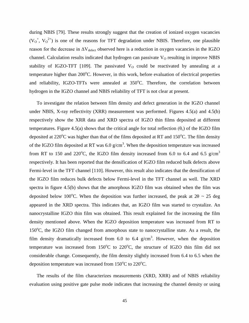
45
during NBIS [79]. These results strongly suggest that the creation of ionized oxygen vacancies
(VO+, VO
2+) is one of the reasons for TFT degradation under NBIS. Therefore, one plausible
reason for the decrease in ΔVdefect observed here is a reduction in oxygen vacancies in the IGZO
channel. Calculation results indicated that hydrogen can passivate VO resulting in improve NBIS
stability of IGZO-TFT [109]. The passivated VO could be reactivated by annealing at a
temperature higher than 200oC. However, in this work, before evaluation of electrical properties
and reliability, IGZO-TFTs were annealed at 350oC. Therefore, the correlation between
hydrogen in the IGZO channel and NBIS reliability of TFT is not clear at present.
To investigate the relation between film density and defect generation in the IGZO channel
under NBIS, X-ray reflectivity (XRR) measurement was performed. Figures 4.5(a) and 4.5(b)
respectively show the XRR data and XRD spectra of IGZO thin films deposited at different
temperatures. Figure 4.5(a) shows that the critical angle for total reflection (θc) of the IGZO film
deposited at 220oC was higher than that of the films deposited at RT and 150
oC. The film density
of the IGZO film deposited at RT was 6.0 g/cm3. When the deposition temperature was increased
from RT to 150 and 220oC, the IGZO film density increased from 6.0 to 6.4 and 6.5 g/cm
3
respectively. It has been reported that the densification of IGZO film reduced bulk defects above
Fermi-level in the TFT channel [110]. However, this result also indicates that the densification of
the IGZO film reduces bulk defects below Fermi-level in the TFT channel as well. The XRD
spectra in figure 4.5(b) shows that the amorphous IGZO film was obtained when the film was
deposited below 100oC. When the deposition was further increased, the peak at 2 ~ 25 deg
appeared in the XRD spectra. This indicates that, an IGZO film was started to crystalize. An
nanocrystalline IGZO thin film was obtained. This result explained for the increasing the film
density mentioned above. When the IGZO deposition temperature was increased from RT to
150oC, the IGZO film changed from amorphous state to nanocrystalline state. As a result, the
film density dramatically increased from 6.0 to 6.4 g/cm3. However, when the deposition
temperature was increased from 150oC to 220
oC, the structure of IGZO thin film did not
considerable change. Consequently, the film density slightly increased from 6.4 to 6.5 when the
deposition temperature was increased from 150oC to 220
oC.
The results of the film characterizes measurements (XRD, XRR) and of NBIS reliability
evaluation using positive gate pulse mode indicates that increasing the channel density or using

46
nanocrystalline IGZO as a channel could inhibits the defect generation in IGZO TFT under NBIS.
As a result, the stability of IGZO TFT under NBIS could be improved.
Figure 4. 5:(a) XRR data, (b) XRD spectra of IGZO thin films deposited at different
temperatures.
In the discussion above, we discussed about the effect of the channel density on the defect
generation in IGZO TFT under NBIS. From now on, we will investigate the effect of the channel
density on the electron trapping at the back channel interface. As shown in figure 4.3(a), 4.3(b)
and 4.3(c), Vrev of TFT-1, TFT-2 and TFT-3 were 18.2, 9.6 and 7.9 V, respectively. Since
trapped electrons at the back channel interface caused the positive shift in Vrev [70], a large
positive Vrev shift in TFT-1 after 104 s NBIS indicates that the back channel interface in TFT-1
was less well formed than those in TFT-2 and TFT-3. It is known that higher sputtering
temperature increases mobility of adatom on the surface, resulting in higher film density and
lower weak-bonding in the film. The weak bonding could have been broken to form the oxygen
vacancy defects by ion bombardment during ES deposition. Therefore, the oxygen vacancy
defects in TFT-1, which were created by ES deposition process, were higher than those in TFT-2
and TFT-3. This result could also explain the dependence of ΔVdefect on IGZO deposition
temperature mentioned above. We would like to note that separating ΔVhole and ΔVdefect from
ΔVh is valuable for further progress in the work to improve NBIS reliability of IGZO TFTs. In
the case of TFT-3, after 104 s NBIS, since ΔVhole was 6.5 V while ΔVdefect was only 1.7V, the

47
contribution of ΔVhole to the hysteresis was 80 percent. Therefore, in future work to improve the
NBIS reliability of this TFT, reducing ΔVhole has stronger effect than reducing ΔVdefect.
4.3.3 Effect of stress temperature on the NBTIS stability of IGZO TFT
As we investigated in previous section, the trapped holes in the GI contributed 80 % of the
hysteresis instability in IGZO TFT under NBIS. Therefore, a reduction of the hole trapping in the
IGZO TFT under NBIS will significantly improve the NBIS reliability of IGZO TFT. Increase
the potential barrier for hole trapping at the GI/IGZO interface is a simple way to reducing the
trapped hole. However, it is difficult to evaluate the energy barrier for hole trapping if the effects
of trapped holes and generated defects on the NBIS instability were not separated.
In this section, we will use PGPM to separate the effects of trapped holes and of generated
defects on the NBIS instability. The potential barrier for hole trapping in at the GI/IGZO
interface will be calculated by studying the effect of stress temperature on IGZO TFT (TFT-3)
under NBITS. Figures 4.6(a), 4.6(b), and 4.6(c) respectively display TFT-3 transfer
characteristics after 104
s NBITS measured using DSM and PGPM at stress temperatures of RT,
35 and 50oC. The durations of the hystereses in TFT-3, which were measured by DSM and
PGPM at the different stress temperatures, are shown in figure. 4.6(d), 4.6(e) and 4.6(f). Both
ΔVhole and ΔVdefect increased with stress temperature. However, stress temperature had a greater
enhancement effect on ΔVhole than on ΔVdefect. After 104 s NBIS, ΔVhole increased from 6.5 to 9.6
V and ΔVdefect increased from 1.7 to 2.9 V when the stress temperature was increased from RT to
50oC as shown in inset figure 4.6(e). The ΔVhole - stress time curves at different temperatures
were well fitted to the commonly used stretched-exponential equation [87]
where Vhole0 is the approximate effective voltage drop across the gate insulator and equals
Vhole at infinity time, represents the characteristic trapping time of carriers
in which τ0 is the thermal pre-factor, thermal activation energy is given by (β is the
stretched-exponential exponent and Eτ is the average effective energy barrier that electrons in the
a-IGZO TFT channel need to overcome to enter the insulator). Insert figure 4.6(f) shows
characteristic trapping time and stretched-exponential exponent as a function of reciprocal stress

48
temperature. The calculated average effective energy barrier (Eτ) was 0.39 eV. The average
effective energy Eτ depends strongly on fabrication conditions and the GI/IGZO interface
property.
Figure 4. 6: Transfer characteristics of TFT-3 after 104 s NBITS at different temperatures (a)
RT, (b) 35oC, and (c) 50
oC. The durations of TFT-3 hysteresis under NBIS at difference
temperatures (d) RT, (e) 35oC (Inset shows dependence of ΔVdefect and ΔVhole on NBITS stress
temperature), and (f) 50oC (Inset shows the value of β and ln(τ) as a function of NBITS stress
temperature).
0
5
10
15
1 200140016001800110001
350deg
Vgs (V)
RRT
0
5
10
15
1 10001
350deg
Vgs (V)0
5
10
15
1 10001
350deg
Vgs (V)
RRT
1.E-141.E-131.E-121.E-111.E-101.E-091.E-081.E-071.E-061.E-05
-10 0 10 20
Id &
Ig (
A)
Vgs (V)
1.E-141.E-131.E-121.E-111.E-101.E-091.E-081.E-071.E-061.E-05
-10 0 10 20
Id &
Ig (
A)
Vgs (V)
1.E-141.E-131.E-121.E-111.E-101.E-091.E-081.E-071.E-061.E-05
-10 0 10 20
Id &
Ig (
A)
Vgs (V)
22oC 35oC 50oC
10-14
10-12
10-10
10-8
10-6
Dra
in c
urr
ent
I DS
(A)
-10 0 10 20 0 10 20Gate Voltage VGS (V)
0 10 20
0
5
10
15
Dra
in c
urr
ent
I DS
(A)
0 5 10 5 10Stress time (x103 s)
5 10
(b)(a) (c)
(d) (e) (f)
0
1
2
7
7.5
8
8.5
3 3.2 3.41000/T
hole
b
τβ
Ln
(τ)
0
5
10
15
3 3.2 3.41000/T
holedefect
DSM
PGPM
1.E-141.E-131.E-121.E-111.E-101.E-091.E-081.E-071.E-061.E-05
-10 0 10 20
Id &
Ig (
A)
Vgs (V)
ipw
DSM
PGPM
Initial
FW REV

49
4.4 Summary
In this chapter, the double sweeping mode and positive gate pulse mode were used to
quantitative analysis the effects of hole trapping and of defect generation on the NBIS instability
in IGZO TFT. The positive gate pulse mode and double sweeping mode were used to separately
measure Vhole and Vdefect. XRD and XRR was used to evaluate the influence of deposition
temperature on structure and film density of IGZO channel. SIMS was used to estimate effects of
deposition temperature on composition of IGZO channel. It was found that the density of IGZO
channel and the relative hydrogen concentration was increased with IGZO deposition
temperature. An amorphous IGZO film was obtained when the deposition temperature was lower
than 150oC. The nano-crystalline IGZO film was obtained when the deposition temperature was
higher than 150oC. The reliability of IGZO TFT under NBIS improved with the deposition
temperature of IGZO channel. We also found that the densification of the IGZO channel reduced
bulk defects below Fermi level in the channel, resulting in the reduction of hysteresis in IGZO
TFT under NBIS. The densification of the channel also reduced the damage at the back channel
interface which was a result of the etching stopper deposition process. As a consequence, the
electron trapping at the back channel interface was reduced. The effects of stress temperature on
the reliability of IGZO TFT under NBITS was also investigated. Stress temperature (in NBITS
test) had a stronger effect on the hole trapping in a GI than on the defect generation in the IGZO
channel. The time dependence of Vhole was well fitted to the commonly used stretched-
exponential equation at different stress temperatures. As a result of separating Vhole and Vdefect
work, the average effective energy barrier of 0.39 eV was calculated. The effective energy
barrier for hole trapping is an importance information for the work to improve the NBIS
reliability because as discovered in chapter 3, the hole trapping is the dominant reason for the
NBIS instability.

50
CHAPTER 5: EFFECTS OF BACK CHANNEL INTERFACE ON NBIS STABILITY
5.1 Introduction
In chapter 4 we considered the effect of channel on the NBIS reliability of IGZO TFT. The
positive gate pulse mode and double sweeping mode were used to quantitatively analyze the
effects of hole trapping and of defect generation on the NBIS instability in IGZO TFT. The
results imply that increasing the film density of IGZO channel reduces the defect generation and
as a consequence, improve the NBIS stability. Since IGZO is a chemically reactive material, the
electrical properties and reliability of IGZO TFT are strongly affected by the post-fabrication
process. In this chapter, we will study the effects of etching stopper deposition condition on the
NBIS reliability of IGZO TFT.
It has been reported that the back channel interface quality strongly affects the initial
properties and reliability of IGZO TFTs. In 2010, Y.Shinhyuk et. al. reported that the
subthreshold swing and NBIS reliability was significantly improved by using Plasma-Enhanced
Atomic Layer Deposition (PEALD) derived AlOx as a passivation layer [111]. By studying the
effects of device configuration on NBIS reliability, Jang.Y.K at. al showed that a TFT with etch
stopper configuration has better electrical properties and NBIS reliability than a TFT with
channel etch configuration. The TEM image of the back channel interface illustrated that the
back channel interface in etch stopper type TFT was better than that in back channel etch type
TFT. The etching stopper has been introduced to prevents the plasma induced damage and
suppress the formation of interfacial by products onto the IGZO layer during the patterning
process of source and drain electrodes [112]. In 2011 Kenji Nomura et. al. reported that the
NBIS reliability of IGZO TFT was significantly improved by using a Y2O3 passivation layer [77].
The reduction of near valance band maximum state at the back channel interface was suggested
as a reason for the NBIS stability improvement. To reduce the damage at the back channel
interface that is induced by post fabrication process, an organic material (CYTOP) has been used
as a passivation layer [113]. Time of flight secondary ion mass spectroscopy (TOF SIMS) has
been conducted to investigate the channel film composition. It has been found that the In, Ga, Zn
ion intensity was relatively smaller and hydrogen ion intensity was higher at the back channel
interface of the SiOx passivated TFT [113]. However, there was no difference in the relative ion

51
intensity ratio between bulk and back channel interface in the CYTOP passivated TFT. As a
result, the electrical properties and reliability of the CYTOP passivated TFT significantly
improved. In 2013, cathode luminescence (CL), ultraviolet photoelectron spectroscopy (USP)
measurement showed that the band bending surface was observed at the back channel [114].
However, due to the lack of a measurement method that can separate the effect of hole trapping
and defect generation on the NBIS instability, the effect of back channel interface on the hole
trapping and on the defect generation was not quantifiable. On the other hand, as we discussed in
chapter 3, the trapped electron at the back channel interface is a reason for the NBIS instability in
IGZO TFT. In this chapter, we will investigate the effects of the back channel interface on the
defect generation and on electron trapping at the back channel interface. The quality of back
channel interface was varied by the PE-CVD plasma power of SiOx etching stopper (ES) deposition.
5.2 Experimental
Bottom-gate top-contact type a-IGZO TFT was fabricated on a glass substrate following
the process described in chapter 3, with the exception of etching stopper deposition condition. A
plasma power of SiOx etching stoper deposition in this experiment was varied as 40 W (TFT-1),
50 W (TFT-2) and 55 W (TFT-3). A light intensity of 0.2 mW/cm2 with a wavelength of 460 nm
and a gate bias voltage of -40 V was applied in NBIS test. DSM and PGPM were used to
measure the transfer characteristic of a-IGZO TFT.
5.3 Results and Discussions
5.3.1 Effects of ES deposition conditions on the initial properties
Figures 5.1(a), 5.1(b), and 5.1(c) show the transfer characteristics of TFT-1, TFT-2 and TFT-
3, respectively. The initial properties of 3 TFTs are listed in table 5.1. Ss values of all TFTs
fluctuated between 0.35 and 0.38 V/decade. However, electron mobility increased from 11.6 to
13.2 cm2/V·s and Vth decreased from 2.8 to 2.1 V when the plasma power of the etching stopper
deposition process was increased from 40 to 55 W. The decrease in Vth that was observed with
the additional plasma power indicates that carrier concentration in the channel was increased
with the plasma power of etching stopper deposition process. The hydrogen and oxygen vacancy
(VO) are known as the electron supplier in IGZO material. As we mentioned in chapter 4,
hydrogen not only acts as a donor in IGZO but also as a carrier scattering point. Therefore,
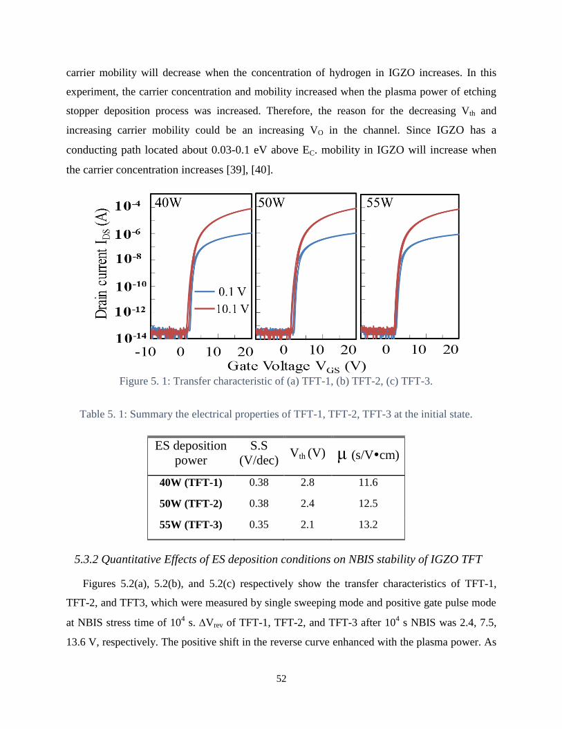
52
carrier mobility will decrease when the concentration of hydrogen in IGZO increases. In this
experiment, the carrier concentration and mobility increased when the plasma power of etching
stopper deposition process was increased. Therefore, the reason for the decreasing Vth and
increasing carrier mobility could be an increasing VO in the channel. Since IGZO has a
conducting path located about 0.03-0.1 eV above EC. mobility in IGZO will increase when
the carrier concentration increases [39], [40].
5.3.2 Quantitative Effects of ES deposition conditions on NBIS stability of IGZO TFT
Figures 5.2(a), 5.2(b), and 5.2(c) respectively show the transfer characteristics of TFT-1,
TFT-2, and TFT3, which were measured by single sweeping mode and positive gate pulse mode
at NBIS stress time of 104 s. Vrev of TFT-1, TFT-2, and TFT-3 after 10
4 s NBIS was 2.4, 7.5,
13.6 V, respectively. The positive shift in the reverse curve enhanced with the plasma power. As
Figure 5. 1: Transfer characteristic of (a) TFT-1, (b) TFT-2, (c) TFT-3.
Table 5. 1: Summary the electrical properties of TFT-1, TFT-2, TFT-3 at the initial state.
ES deposition
power
S.S
(V/dec) Vth (V) μ (s/Vcm)
40W (TFT-1) 0.38 2.8 11.6
50W (TFT-2) 0.38 2.4 12.5
55W (TFT-3) 0.35 2.1 13.2

53
discussed in chapter 3 and chapter 4, the electron trapping at the back channel interface caused
apositive shift in reversed curve. Therefore, the enhancement of the positive shift, which is
shown in figure 5.2(a), 5.2(b), and 5.2(c), implies that the back channel in TFT-3 was less well
formed than that in TFT-1. This suggests that the etching stopper deposition condition,
particularly in the plasma power of etching stopper deposition process, strongly affected the
quality of the back channel interface.
We also used positive gate pulse mode and double sweeping mode to quantitatively analyse
the effects of the plasma power of etching stopper deposition process on the hole trapping and
defect generation in IGZO TFT under NBIS. Figures 5.2(c), 5.2(d), and 5.2(e) represent the
hysteresis induced by trapped holes at the front channel interface and by generated defects in the
channel. The hysteresis induced by the generated defects increased from 0.9 to 3.3 V when the
plasma power was increased from 40 to 50 W. The hysteresis induced by the generated defects
was further increased to 4.7 V when the plasma power was raised to 55 W. These results suggest
that etching stopper deposition conditions had a strong impact on defect generation in IGZO
TFTs under NBIS. As we pointed out in the last paragraph, increasing the plasma power reduced
the quality of back channel interface. Therefore, the increasing hysteresis induced by the
generated defects implies that there is a strong correlation between back channel interface
qualities and defect generation in IGZO TFT under NBIS. In other words, by separating the
effects of hole trapping and defect generation on the NBIS induced hysteresis, we confirmed that
the defects were meanly generated at the back channel interface. The etching stopper deposition
conditions not only influence defect generation in the channel but also electron trapping at the
back channel interface. Therefore, in the work to improve the NBIS stability, the etching stopper
deposition condition needs to be optimized.
In spite of the hysteresis induced by generated defects, the hysteresis induced by trapped
holes at the front channel interface was 2.9 V regardless of the plasma power of etching stopper
deposition process. The energetic bombardment of negative oxygen ion, which was accelerated
by the applied electric field between the substrate and the target in DC magnetron sputtering, was
found to be the reason for the GI/channel interface damage [106], [107]. In this work, the gate
insulator and channel in all TFT was deposited under the same conditions. Therefore, the
qualities of IGZO/GI interface are assumed to be the same for all TFTs. On the other hand, it is
54
also well established that trapped carriers at the front channel interface are mainly determined by
gate bias stress and the front channel interface quality [87], [88]. At the same gate voltage stress
and IGZO/GI interface quality, the hole trapping at front channel interface are approximately
equal for all TFTs. As a result, hystereses measured using positive gate pulse mode from TFT-1,
TFT-2 and TFT-3 were almost identical. Since the measurement results are in good agreement
with the theoretically predicted results; positive gate pulse mode can be used for an estimation of
ΔVhole in the IGZO TFT under NBIS. This result and the result shown in chapter 4 are evidence
that the positive gate pulse mode and double sweeping mode can be used to accurately
quantitatively analyse the effect of hole trapping and of defect generation on the NBIS instability in
IGZO TFT.
5.4 Summary
In this chapter, double sweeping mode and positive gate pulse mode were used to investigate
the effects of plasma power of etching stopper deposition process on the NBIS instability in
IGZO TFT. It was found that the plasma power of etching stopper deposition process strongly
affected the initial characteristics and NBIS reliability of IGZO TFTs. The field effect mobility
of IGZO TFT increased but TFT threshold voltage decreased with the plasma power of etching
stopper deposition process. The NBIS reliability improved when the plasma power was increased.
The plasma power of PECVD in etching stopper deposition process created some damage at the
back channel interface. Under NBIS, the defects were mainly generated at the back channel
interfaces and defect generation could be controlled by the etching stopper deposition conditions.
The results in this chapter further our thesis that hole trapping at the front channel interface is the
main cause of the NBIS instability in IGZO TFT. Therefore, in following chapter we will discuss
the hole trapping mechanism and the method to significantly improve the NBIS stability of
GIZO TFT.

55
Figure 5. 2: Figure 4. 7: Transfer characteristic of (a) TFT-1, (b) TFT-2, (c) TFT-3 after 10
4 s
NBIS measured using double sweeping mode and positive gate pulse mode, and duration of
hysteresis detected using double sweeping mode and positive gate pulse mode in (d) TFT-1,
(e) TFT-2, (f) TFT-3 under NBIS

56
CHAPTER 6: A DRIVING METHOD TO IMPROVE THE NBIS RELIABILITY
6.1 Introduction
As we discussed in previous chapters, the trapped holes in gate insulator [67], [74], [75],
[90], the generated ionized oxygen vacancies (Vo+, Vo
2+) and created defects in the channel are
widely accepted as reasons for the NBIS instability [76]–[80], [105]. To date, material approach
has been applied to improve the NBIS stability. The trapped holes could be reduced by a GI
material which has high hole trapping barrier such as SiOx or AlOx [115]. A TiO2 film which
acts as hole carrier blocking layer was also used to inhibit the hole trapping [116]. High pressure
water [91], [92], wet O2 annealing [93], Y2O3 passivation layer [77]… have been used to
passivate VO defects. However, suppressing VO defects in amorphous IGZO remains a challenge
due to high density of state of VO defects in IGZO. Therefore, a new approach is needed to
achieve highly reliability IGZO TFT under NBIS. To do that, the detail of the NBIS degradation
mechanism is required to be investigated. In this chapter, the NBIS degradation mechanism was
clarified by investigating the effect of negative pulse duration in AC gate bias and of incident
light intensity on the NBIS degradation behavior. Based on a investigated hole generation
mechanism, a control algorithm was proposed to improve the NBIS stability.
6.2 Experimental
Bottom-gate top-contact IGZO TFTs with a channel width/length of 800 μm/160 μm were
fabricated on a glass substrate. Detail of the fabrication process is shown in figure 6.1. 50-nm-Cr
gate electrodes were deposited on the substrate by DC-sputtering and then patterned by wet-
etching. A stack 160-nm-SiNx:F/50-nm-SiOx GI was deposited by Inductively Plasma-Enhanced
Chemical Vapor Deposition (ICP-CVD)/Plasma-Enhanced Chemical Vapor Deposition (PE-
CVD), respectively. 45-nm-IGZO channels were deposited on the GI by DC-sputtering and then
patterned by dry-etching. A 200-nm-SiOx etching-stopper was subsequently deposited by PE-
CVD. 50-nm Indium Tin Oxide (ITO) source/drain electrodes were deposited by DC-sputtering
and then patterned by dry-etching. A 200-nm-SiOx passivation layer was then deposited by PE-
CVD. After that the devices were annealed for 1 hour in N2 ambient at 350oC. The electrical
properties and reliability of IGZO TFT were evaluated using an Agilent 4156C semiconductor

57
analyzer. A gate bias stress of -30 V with blue light ( = 460 nm) at a power density of 0.2
mW/cm2 was applied in NBIS testing.
Figure 6. 1: Fabrication process of IGZO TFTs with a SiNx:F/SiOx gate stack layer
6.3 Results and Discussions
6.3.1 Effects of Positive gate pulse on the NBIS stability of IGZO TFT
Figure 6.2 shows the initial transfer characteristic (ID - VG) of IGZO TFT measured by
double sweeping mode at a drain voltage VD of 0.1 and 10.1 V. The linear mobility was ~19
cm2/Vs. Threshold voltage (Vth) of ~6 V is defined as the gate voltage at drain current ID = 1 nA.
Subthreshold swing (Ss value) of ~0.2 Vdec-1
is defined as the gate voltage required to increase
ID from 0.1 to 1 nA. Hysteresis (Vh) is defined as the difference in Vth between forward (Vfw) and
reverse (Vrev) sweeps. The Vh at initial state was 0.2 V.

58
Figure 6. 2: Initial transfer characteristic of IGZO TFT with stack gate insulator
Figure 6.3(a) shows the change in the TFT’s transfer characteristics as measured by the
single sweeping mode under DC-NBIS. The transfer curve shifted -4.3 V (in negative direction)
with Ss degradation. The Ss degradation indicates that the defects were created in the TFT. To
further investigate the reason for this negative shift in transfer curve, a positive gate pulse mode
(PGPM) was conducted [90], [105]. The PGPM is a transfer characteristic measurement method
in which a positive gate pulse is applied to the TFT prior to transfer characteristic measurements.
As we discussed in previous report [105], a positive gate pulse not only stabilizes the created
defects but also detraps holes from the GI. Therefore, in order to stabilize the created defects and
to minimize the hole detrapping from the GI, a positive gate pulse with a pulse width of 1 ms and
a pulse high of 10 V was chosen. Figure 6.3(b) shows the change in the TFT’s transfer
characteristics measured by PGPM as a function of the NBIS duration. The transfer
characteristics measured by the PGPM negatively shifted without Ss degradation. Based on the
results of our previous work [78], [105], the created defects are the ionized types of oxygen
vacancies (VO+, VO
2+). The positive gate pulse causes electron to accumulate in the channel. The
VO+, VO
2+ are simultaneously stabilized by capturing the accumulated electrons. As a result, the
Ss value did not degrade in the transfer curve measured by PGPM. As a consequence of the VO+,
VO2+
stabilization, trapped holes in the GI caused a negative shift in the transfer curve as
measured by PGPM. The threshold voltage shift (Vth) at 104 s DC-NBIS measured by PGPM

59
was -3.6 V. The results and discussions above indicate that the trapped holes in the GI and
created defects (VO+, VO
2+) in the TFTs are reasons for the Vth instability in the IGZO TFT under
DC-NBIS. It also shows that Vth at the DC-NBIS duration of 104 s increased from -4.3 to -3.6V
when the positive gate pulse was applied prior to transfer characteristic measurement. This mean
that the NBIS stability in IGZO TFT improved by applying a positive gate pulse. This
improvement in the NBIS stability is caused by the defect stabilization.
Figure 6. 3: Change in transfer characteristic of IGZO TFT under DC-NBIS measured by (a)
single sweeping mode, and (b) positive gate pulse mode.
In order to further investigate the influences of the positive gate pulse on the NBIS stability,
-30 V negative gate and 10 V positive gate pulse high was alternatively applied as a gate bias
stress (AC-NBIS). The positive gate pulse width was fixed as 1 ms. The negative gate pulse
width was varied from 100 s to 1000 s. Table 6.1 shows gate bias conditions which were applied
in AC-NBIS testing. The stress time for AC-NBIS is defined as a total negative gate pulse
duration. Figures 6.4(a)-6.4(d) show the change in IGZO TFT’s transfer characteristic in under
AC-NBIS with a negative gate pulse width of 100, 200, 250, 500 s, respectively. In all cases, the
transfer characteristic shifted negatively without a considerable change in the Ss value. This
result implies that trapped holes in the GI are the main cause of the shift in TFT’s transfer
characteristic under AC-NBIS. Figure 6.4(e) shows the AC-NBIS stress time dependent of Vth
for different gate bias conditions. The dependence of Vth at the AC-NBIS stress time of 104 s
on the negative gate pulse width is shown in figure 6.4(f). The Vth slightly decreased from -0.6
to -0.7 V when the negative gate pulse width was increased from 100 to 200 s. However, when

60
Figure 6. 4: Change in transfer characteristic under AC-NBIS with different gate bias condition;
(a) NBIS-1, (b) NBIS-3, (c) NBIS-4, (d) NBIS-5. (e) the stress time dependence of Vth under
NBIS, (f) the Vth at the AC-NBIS duration of 104 s as a function of negative pulse width.

61
the negative gate pulse width was further increased to 250 s, the Vth rapidly decreased to -1.7
V. Figure 6.4(f) shows that a linear relationship between Vth at the AC-NBIS stress time of 104
s and logarithmic of the negative pulse width was observed. When the negative gate pulse width
was varied from 100 to 200 s, the slope of Vth - log(pulse width) was -1. The slope increased to
-3.1 when the negative gate pulse width was varied from 250 to 1000 s. This result suggests that
the hole trapping barrier reduced when the negative pulse width exceeded 250 s. In previous
report [75], the reliability of IGZO TFT under 25 kHz-AC-NBIS has been investigated. Cheng
et. al. has suggested that due to low hole mobility in IGZO, the duration of negative gate voltage
in the 25 kHz-AC gate bias stress does not provide enough time for holes to drift to the front
channel interface. As a result, the TFT was stable under the 25 kHz-AC-NBIS. However, in this
work the IGZO TFTs were almost stabled even though a negative gate pulse width of 200 s was
used. This negative gate period may provide enough time for the holes to drift to the front
channel interface. Therefore, the low hole mobility in IGZO is not enough for explain the results
shown in figure 6.4(e) and 6.4(f).
6.3.2 Hole generation mechanism
In order to clarify the reasons that the positive gate pulse improved the gate bias illumination
stress stability, we compared the transfer characteristics measured at the DC-NBIS stress time of
200 and 250 s. Figures 6.5(a) and 6.5(b) illustrate TFT’s transfer characteristics measured by
single sweeping mode (without applying the positive gate pulse) at a light intensity of 0.2
mW/cm2 and the DC-NBIS duration of 200 and 250 s, respectively. The TFT transfer
characteristics measured by PGPM (with applying the positive gate pulse) at the stress time of
200 and 250 s are shown in figure 6.5(c) and 6.5(d), respectively. All transfer curves measured
by SSM shifted negatively with an Ss degradation. The Ss degradation indicates that the VO+,
VO2+
defect was generated. When the positive gate pulse was applied, the transfer curve
recovered to the initial state in the case of DC-NBIS duration of 200 s, as shown in figure 6.5(c).
This result suggests that, the VO+, VO
2+ defects, which can be stabilized by the positive gate pulse
[105], are the reason for the negative shift in transfer curve after 200 s DC-NBIS. The density of
the trapped holes in the GI after 200 s DC-NBIS was not sufficient to effect the Vth. As a
consequence, the IGZO TFT was almost stable under AC-NBIS, as shown in figure 6.4(a) and
6.4(b). By contrast, figure 6.5(d) shows that the transfer curve measured at the NBIS duration of

62
250 s shifted -0.3 V when the positive gate pulse was applied. This result indicates that the
density of the trapped holes in the GI increased dramatically when the NBIS duration was further
increased to 250 s. Consequently, the Vth at the AC-NBIS duration of 104 s rapidly decreased
from -0.7 to -1.7 V when the negative pulse width was increased from 200 to 250 s, as shown in
figure 6.4(f).
Figure 6. 5: The transfer characteristic of IGZO TFT measured before applying the positive
gate pulse at light intensity of 0.2 mW/cm2 and the DC-NBIS duration of (a) 200 s, (b) 250 s.
The transfer characteristic of the IGZO TFT measured after applying the positive gate pulse at
the DC-NBIS duration of (a) 200 s, (b) 250 s.
In order to investigate the reason for that the density of trapped holes dramatically increased
when the NBIS duration reached 250s, the effect of light intensity on the Vth at the stress time
of 250 s was investigated. The light intensity was varied from 0.1 to 0.4 mW/cm2. Figures 6.6(a)
and 6.6(b) illustrate the TFT’s transfer characteristics measured by SSM at the light intensity of
0.1 and 0.4 mW/cm2, respectively. The TFT’s transfer characteristics measured by PGPM at the

63
light intensity of 0.1 and 0.4 mW/cm2 are shown in figure 6.6(c) and 6.6(d), respectively. When
the light intensity was set as 0.1 mW/cm2, the transfer curve measured without applicant of the
positive
Figure 6. 6 The transfer characteristic of IGZO TFT at the DC-NBIS duration of 250 s
measured before applying the positive gate pulse with a light intensity of (a) 0.1 mW/cm2, (b)
0.4 mW/cm2. The transfer characteristic of the IGZO TFT at the DC-NBIS duration of 250 s
measured after applying the positive gate pulse with a light intensity of (a) 0.1 mW/cm2, (b)
0.4 mW/cm2.
gate pulse was shifted slightly. The Ss degraded at the drain current below 10 pA. The transfer
curve recovered to the initial state when the positive gate voltage was applied, as shown in figure
6.6(c). This indicates that the number of trapped holes in the GI could be negligible. When the
light intensity was increased to 0.4 mW/cm2, the negative shift in the transfer curve measured by
SSM enhanced. The Ss degraded at the drain current below 10 nA. This result suggests that the

64
energy distribution of VO+, VO
2+ increased, to a level closer to the conduction band minimum
(EC). When the positive gate voltage was applied prior to transfer characteristic measurement,
the Ss degradation vanished. Vth of -0.8 V was observed. The Vth measured by PGPM
decreased from -0.3 to -0.8 V when the light intensity was increased from 0.2 to 0.4 mW/cm2, as
shown in figure 6.5(d) and 6.6(d). This result indicates that the trapped holes in the GI not only
depend on the negative gate voltage duration but also depend on the incident light intensity.
The influences of negative gate pulse width and of incident light intensity on trapped holes in
the GI suggest the presence of a hole trapping process in the TFT under NBIS, which is shown in
figure 6.7. The hole trapping process includes 2 steps: hole generation in the channel and hole
injection into the GI. At the early stage of NBIS, the blue incident light (hν = 2.7 eV) excites
electrons from Vo defects (located about 2.3 eV from EC) to conduction band [38], [82], [108],
[117], and generates VO+, VO
2+, as shown in figure 6.7(a). The VO
+, VO
2+ act not only as the
donor-like defects but also as the midgap trap states. The incident photon then induces an optical
excitation of electron from the valence band maximum to the midgap trap states, and generates
free hole. The generated holes are accumulated at the front channel interface and injected to the
GI under a negative gate bias stress. The detail of hole generation is illustrated in figure 6.7(b).
The hole generation mechanism suggests that number of generated holes not only depends on the
light intensity but also on the DOS of midgap trap states (VO+, VO
2+). At the early stages, the
generated hole density is low due to low emission rate of deep states in IGZO [118]. The hole
trapping is limited by the hole generation step, resulting in the slope of -1 shown in figure 2(f).
On the other hand, when NBIS duration was increased, the DOS of Vo+, Vo
2+ exponentially
increased. The probability of Vo+, Vo
2+ capturing the excited electron also dramatically increased.
Therefore, the hole trapping process is limited by the hole injection step, resulting in the slope of
-3.1 shown in figure 6.4(f). The hole generation mechanism implies that a reduction in DOS of
the midgap trap states can reduce the trapped holes in the GI, resulting in an improvement in the
NBIS stability. The DOS of midgap trap states can be reduced either by suppresing deep subgap
defects[77], [92], [96], by inducing recombination centers in channel (material approach)[119] or
by control algorithm, as shown in this work (the driving approach). The discussions above also
imply that the reliability of IGZO TFT can be significantly improved when the display is
working at a high frame rate. Long refresh time is an advantage of IGZO display. However, the
results of this work suggest that the long refresh time reduces the stability of IGZO display. In

65
order to improve the NBIS reliability and reduce the power consumption of the IGZO displays,
an optimal refresh time is required.
Figure 6. 7: (a) the defect generation mechanism, (b) the hole generation mechanism
6.4 Summary
This chapter presents a method to improve the NBIS reliability of IGZO TFT. The
degradation behavior and the degradation mechanism of IGZO TFT under AC- and DC-NBIS
were investigated. Effects of the negative pulse width and of light intensity on the NBIS
reliability were also examined. The NBIS reliability significantly improved when either the
negative pulse width was reduced or intensity of the stress light was decreased. A linear
relationship between Vth at the AC-NBIS stress time of 104 s and logarithmic of the negative
pulse width was observed. When the negative gate pulse width was varied from 100 to 200 s, the
slope of Vth - log(pulse width) was -1. The slope increased to -3.1 when the negative gate pulse
width was varied from 250 to 1000 s. The hole trapping in the GI was found to be the reason for
the AC-NBIS instability. The created defects act as the midgap trap state for hole generation.
However, these created defects are stabilized by capturing electrons. These results suggest that
the NBIS reliability of IGZO TFT can be significantly improved by increasing the frame rate of
FPD. The refresh time also needs to be optimized to achieve NBIS reliability.
GI +
+
+
Gate
Vg < 0 V
- - -- ---
+++ ++
hv
(b)
VO2+
VO+
GI
Gate
Vg < 0 V
- - -- ---
hv
(a)

66
CHAPTER 7: PBS DEGRADATION MECHANISM AND METHOD TO IMPROVE THE PBS
RELIABILITY
7.1 Introduction
In FPDs, a positive voltage is applied to the gate electrode when TFT is operated at the on-
state. The TFTs are worked under positive bias stress (PBS). Therefore, the reliability of TFTs
under PBS is required for a display application. Even thought, the reliability of IGZO TFTs
under positive bias stress is not so serious problem as compared with the NBIS reliability.
However, the reliability of IGZO TFT under PBS also needs improvement. The PBS reliability
of IGZO TFT has gathered attention of many researchers. Trapped electrons at a front channel
interface or in a gate insulator (GI) have been accepted as a reason for PBS instability in an
IGZO TFT. The hole trapping mechanism has suggested due to the fact that the change in Vth
with PBS duration was well fitted to a stress exponential equation [120], [121]. Different gate
dielectric materials have been used to reduce the trapped electrons, resulting in an improvement
in the PBS stability. It was reported that a SiOx and an AlOx GI significantly improve the PBS
stability of the IGZO TFT [122], [123]. Besides the electron trapping at the front channel
interface, shallow traps and deep traps have also been suggested as a possible reason for the
positive threshold voltage (Vth) shift in an IGZO TFT under PBS [124], [125]. The acceptor-like
deep traps at 1.0 eV below the conduction band minimum were introduced to simulate
experimental results [124]. A study on the activation energy of electron trapping and of
detrapping (recovery process) under PBS predicted creation of deep acceptor-like defects in the
TFT under PBS, but the energy level of the created defects has not yet been determined [100].
Dry, wet, O2, O3 annealing, hydrogen, nitrogen, fluorine treatment, and titanium metal reaction
methods have been used to reduce the trap sites in the bulk or at the front channel interface [92],
[94], [101], [124], [126]–[130]. Nonetheless, in our best knowledge, direct evidence for the
created deep defects and the energy level of the created defects has not been reported yet. This is
due to the fact that the trapped electrons at the front channel interface and the created deep
defects induce the same degradation behavior in transfer and C-V characteristics. Therefore, it is
difficult to distinguish the effect of the trapped electrons and of the created deep defects on the
PBS instability. In this work, the conductance measurement method [131] was used to
investigate the effect of the post-annealing time on PBS degradation mechanism. We found that,

67
stabilization of the donor-like interface defects is a reason for PBS instability of the IGZO TFT.
The created deep acceptor-like interface defects were identified by the trap time constant. The
energy distribution and trap time constant of the acceptor-like interface defects were also
extracted. The experimental results show that the PBS stability of IGZO TFTs could be
improved by increasing the post-annealing time.
7.2 Experimental Details
The IGZO TFT fabrication process has been described in our chapter 3. Before electrical
measurement and reliability evaluation, the IGZO TFTs were annealed in N2 ambient at 350oC
for 1 hour (sample A1) and 5 hours (sample A2). A gate bias stress of 30 V with a grounded
source and drain was applied in the PBS test. The electrical properties and reliability of IGZO
TFTs were evaluated using an Agilent 4156C semiconductor parameter analyzer. The
capacitance, conductance and admittance was measured using a computer controlled Agilent
4980A Precision LCR Meter at frequencies ranging from 100 Hz to 2 MHz. Schematic of the
measurement is shown in figure 7.1. Threshold voltage (Vth) is defined as the gate voltage at a
drain current (ID) of 1 nA. Subthreshold swing, which is extracted near the Vth region, is defined
as the gate voltage required to increase ID from 0.1 to 1 nA.
Figure 7. 1: Schematic diagram of the PBS testing and conductance measurement
7.3 Results and Discussion
7.3.1 Effect of Post-Annealing Time on Initial Transfer Characteristic and Positive Bias
Stress Stability
Figure 7.2(a) and 7.2(b) show the transfer characteristics of the sample A1 and A2,
respectively. The change in transfer characteristic of the sample A1 and A2 under PBS are
shown in figure 7.2(c) and 7.2(d), respectively. Vth of ~1.3 V, mobility of ~12 cm2/Vs, and Ss

68
value of ~0.1 Vdec-1
were not considerably different between sample A1 and A2. This result
indicates that the front channel interface quality of sample A1 is similar to that of sample A2.
The effect of post-annealing time on the initial properties of IGZO TFTs can be negligible. In
spite of the initial properties, PBS reliability of the IGZO TFT considerably improved with the
post-annealing time, as shown in figure 7.2(c) and 7.2(d). When the post-annealing time was
increased from 1 to 5 hrs, Vth after 104 s PBS reduced from 4.3 to 3.5 V. In order to investigate
the causes of this PBS reliability improvement, the density of state (DOS) of the front channel
interface (Di) with the PBS duration was evaluated. Low-high capacitance voltage measurement
is one of the most popular techniques for analyzing semiconductor/insulator interface properties
[127], [132]. However, these capacitance based extraction methods cannot provide the properties
of defects such as trap time constant, capture cross section. Therefore, it is difficult to distinguish
the defects which have overlapping energy distribution. In this work, the conduction method is
chosen to extract the Di not only because the conductance method is known as the most
complete, high sensitivity, accurate method to characterize interface trap properties but also
because the conductance method can provide the trap time constant of the defects [60], [64],
[133]–[136].
The conductance method is based on measuring the parallel conductance of a metal
insulator semiconductor as a function of gate bias and frequency. The density of interface
defects and their properties can be obtained by fitting the measurement results to a theoretical
model. The series resistance and bulk states could affect the measured conductance, but these
factors could be taken in to account in the fitting model. In this work, we assumed that the
interface traps are distributed continuously across the IGZO bandgap. Therefore, the
equation describing a relationship between parallel conductance (Gp) and frequency (f) of the
applied AC signal is [131]
(1)
Where angular frequency = 2f, i is interface trap time constant. The Di and i can be
extracted from the peak intensity and the peak position of the Gp/ versus -1 curve. The
DOS of an interface trap states and the interface trap time constant can be calculated using
the following formula [137]:
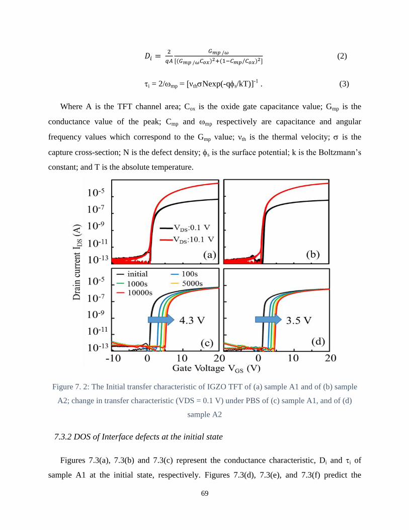
69
(2)
i = 2/mp = [νthNexp(-qs/kT)]-1 . (3)
Where A is the TFT channel area; Cox is the oxide gate capacitance value; Gmp is the
conductance value of the peak; Cmp and mp respectively are capacitance and angular
frequency values which correspond to the Gmp value; νth is the thermal velocity; is the
capture cross-section; N is the defect density; s is the surface potential; k is the Boltzmann’s
constant; and T is the absolute temperature.
Figure 7. 2: The Initial transfer characteristic of IGZO TFT of (a) sample A1 and of (b) sample
A2; change in transfer characteristic (VDS = 0.1 V) under PBS of (c) sample A1, and of (d)
sample A2
7.3.2 DOS of Interface defects at the initial state
Figures 7.3(a), 7.3(b) and 7.3(c) represent the conductance characteristic, Di and i of
sample A1 at the initial state, respectively. Figures 7.3(d), 7.3(e), and 7.3(f) predict the

70
conductance characteristic, Di and i of sample A2 at the initial state, respectively. The Di
interrupted at the applied DC gate voltage (Vg) of 1.8 V as shown in figure 7.3(b), 7.3(e),
similarly to i as shown in figure 7.3(c), 7.3(f). The i either exponentially depended on the
applied gate voltage (represented by the orange color in the figure) or did not depend on the
applied gate voltage (represented by the blue color in the figure). This suggests that those are
different kind of interface defects. In order to classify the origin of the interface defects, the
capacitance voltage (C-V) measurement at a frequency of 100 Hz was conducted to
determine the flat band voltage. Figures 7.4(a) and 7.4(c) respectively show the C-V curve of
sample A1 and of sample A2. Figures 7.4(b) and 7.4(d) represent the relationship between
surface potential and gate voltage in sample A1 and in sample A2, respectively. Figures
7.3(b) and 7.3(e) show that the Di and i were interrupted at the Vg near the flat band voltage
(VFB). Therefore, the defects which locate above VFB are the acceptor-like interface defects.
The defects which locate below VFB are donor-like interface defects. The Di of the acceptor-
like interface defects fluctuated between 1x10¹² and 1.5x10¹² eV-1cm-2 and distributed
uniformly, as shown in figure 7.3(b) and 7.3(e). This Di value is comparable to previous
reports [138]–[141]. The Di dispersion can be attributed to a surface potential (s)
fluctuation, which is caused by accumulated electrons at the front channel interface. The i of
the acceptor-like interface defects was proportional to 1/exp(~ s), and this is consistent with
the equation (7.3). The extracted Di of the donor-like interface defects of the sample A1
(~1.3x10¹¹ eV-1cm-2) and of the sample A2 (1.4x10¹¹ eV-1cm-2) were not considerably
different as shown in figure 7.3(b) and 7.3(e). This result implies that the influence of the
post-annealing time on the DOS of interface defects in the IGZO TFT was negligible. In
spite of the i of the acceptor-like interface defects, figure 7.3(c), 7.3(f) show that the i of the
donor-like interface defects did not depend on surface potential or Fermi level. The
independence i of the donor-like interface defects on surface potential is not consistent with
the equation (7.3), as in equation (7.33) the i is proportional to 1/exp(~ s). Therefore, the
donor-like interface defects mentioned here could not only refer to the defects at the front
channel interface but also refer to the donor-like defects that exit in the SiOx GI within
tunneling distances (<50 Ao) of the front channel interface [131], [142]. From here on, the
71
term interface defects refers to defects both at the front channel interface and in the SiOx near
interface within tunneling distances. The interface defects could electrically communicate
with the channel by tunneling [143], [144]. The i could be calculated by equation [134],
[145]:
(7.4)
Where d is the length of the electron tunnel (or distance between the front interface and
the defects in the insulator), K1 is the wave vector of carriers inside insulator, and (d=0) is
the time constant of the states at the interface. Equation 7.44 indicates that the trap time
constant does not depend on surface potential. This could be explained by the independence
i of the donor-like interface defects on surface potential that is shown in figure 7.3(c) and
7.3(f). Figures 7.3(c) and 7.3(f) also show that the i of the donor-like interface defects of the
sample A1 (~ 2x10⁻⁷ s) was lower than that of the sample A2 (~ 1x10⁻⁶ s). This means that
long time post-annealing increases the trap time constant of the donor-like interface defects.
The results and discussions above also imply that the extracted i of the interface defects
from conductance measurement is an important parameter for classifying the defects. The
acceptor-like and the donor-like interface defects, which overlap each other near VFB, could
be distinguished by the i.

72
Figure 7. 3: A set of Gm/ versus f curves with different applied DC gate voltage for (a)
sample A1, and for (d) sample A2 at initial state; the distribution of Di as function of applied
DC gate voltage for (b) sample A1, and for (e) sample A2 at initial state; the variation of i as
function of applied DC gate voltage for (c) sample A1, and for (f) sample A2 at initial state.

73
Figure 7. 4: Capacitance - gate voltage curve of (a) sample A1, of (c) sample A2 and surface
potential - gate voltage relationship of (b) sample A1, of (d) sample A2.
7.3.3 PBS degradation mechanism of 1 hour post-annealing sample
In order to investigate the relationship between the interface defects and the positive shift in
the transfer characteristic of sample A1 under PBS, conductance measurement was conducted.
The flat band voltage of sample A1 after PBS stress was also extracted. Figures 7.5(a) and
7.5(c) respectively show the C-V curve of sample A1 at the PBS duration of 1000 and
5000 s. Figures 7.5(b) and 7.5(d) represent the relationship between surface potential and
gate voltage in sample A1 at the PBS stress time of 1000 and 5000 s, respectively. A
conductance characteristic, Di and i of the sample A1 at the PBS stress time of 1000 s are

74
respectively illustrated in figure 7.6(a), 7.6(b), and 7.6(c). Figures 7.6(d), 7.6(e), and 7.6(f) show
a conductance characteristic, Di and i of the sample A1 at the PBS stress time of 5000 s,
respectively. Figures 7.6(b), 7.6(b), and 7.6(e) show that the DOS of acceptor-like interface
defects did not change with PBS duration. However, the donor-like interface defects disappeared
with the PBS stress time. A vanishing of the donor-like defects reduced the positive charges at
the front channel interface, resulting in a positive shift in the transfer curve shown in figure
7.2(c). Under PBS, the donor-like interface defects were able to capture electrons and become
electrically inactive; as a consequence, the donor-like interface defects disappeared in the
conductance characteristic. This result indicates that the stabilization of the donor-like interface
defects is the dominant degradation mechanism in the sample A1 under PBS. The donor-like
defects at the IGZO/GI interface or in GI near interface act as electron trapping centers. It is
noted that the donor-like defects located near the valence band minimum are less stable than
those located near the Femi level. Therefore, the donor-like defects located near the valence band
minimum will be stabilized more easily.

75
Figure 7. 5: Capacitance - gate voltage curve of sample A1 after (a) 1000 s PBS, (c) 5000 s
PBS and surface potential - gate voltage relationship of sample A1 after (b) 1000 s PBS, (d)
5000 s PBS.

76
Figure 7. 6: A set of Gm/ versus f curves with different applied DC gate voltage for (a)
sample A1 after (a) 1000 s , (d) 5000 s PBS; the distribution of (b) Di, and (c) i as function of
aplied DC gate voltage in sample A1 after 1000 s PBS; the distribution of (e) Di, and (f) i as
function of aplied DC gate voltage in sample A1 after 5000 s PBS.

77
7.3.4 PBS degradation mechanism of 5 hours post-annealing sample
Figures 7.7(a) and 7.7(c) respectively show the C-V curve of sample A2 at the PBS
duration of 1000 and 5000 s. Figures 7.7(b) and 7.7(d) represent the relationship between
surface potential and gate voltage in sample A2 at the PBS stress time of 1000 and 5000
s, respectively. The change in Di with the PBS duration was analyzed to investigate the reasons
for the improvement in PBS stability in sample A2. Figures 7.8(a), 7.8(b) and 7.8(c) represent a
conductance characteristic, Di and i of the sample A2 at the PBS stress time of 1000 s,
respectively. Figures 7.8(d), 7.4(e) and 7.8(f) depict a conductance characteristic, Di and i of the
sample A2 at the PBS stress time of 5000 s, respectively. Unlike in sample A1, the DOS of the
donor-like interface defects in sample A2 slightly decreased, from 1.4x10¹¹
eV-1
cm-2
at the initial
state to 1.3x10¹¹
eV-1
cm-2
at the PBS stress time of 5000 s, as shown in figure 7.3(e), 7.8(b) and
7.8(e). These results indicate that in sample A2, the donor-like interface defects are stable under
PBS. As discussed in the previous paragraph, the donor-like interface defects are stabilized by
capturing electrons. Therefore, the stability of the donor-like interface defects in the sample A2
under PBS suggests that electrons were difficult to trap at the front channel interface. In other
words, long time annealing improves the electron trapping resistivity at the IGZO/SiOx interface,
resulting in an improvement in PBS stability. Figures 7.3(f), 7.8(c), 7.8(f) show that the i of the
donor-like interface defects also reduced, from ~1x10⁻⁶
to 6x10⁻⁷
s, when PBS stress time was
increased from 0 (initial state) to 5000 s. Equation (7.4) suggests that this reduction in i could be
related to a reduction in the tunneling distance. As shown in figures 7.3(d), 7.8(a) and 7.8(d), the
conductance characteristic at the PBS duration of 1000 and of 5000 s appeared new peaks. The
distribution of Di and i (represented by the red color) extracting from the new peaks are
respectively shown in figure 7.8(b) and 7.8(c) for the PBS stress time of 1000 s and in figure
7.8(e) and 7.8(f) for the PBS stress time of 5000 s. Figures 7.8(c) and 7.8(f) show that the s
dependence of i of the created defects was similar to that of the acceptor-like interface defects
(represented by the orange color). This suggests that the new peaks associate with created
acceptor-like defects at the front channel interface. The created acceptor-like defects locate
below Fermi level and act as electron trap states at the front channel interface, resulting in a
positive shift in the TFT transfer characteristic. The Di of the created acceptor-like defects in the
sample A2 at the PBS stress time of 1000 s exponentially increased from 0.7 x10¹⁰
to 7.6x10¹⁰

78
eV-1
cm-2
when the applied gate voltage was increased from 1.6 to 2.6 V, as shown in figure
7.8(b). Figure 7.8(f) shows that the Di of the created acceptor-like defects in sample A2 at the
PBS stress time of 5000 s exponentially increased from 1.1x10¹⁰
to 1.7x10¹¹
eV-1
cm-2
when the
applied gate voltage was increased from 2.2 to 3.6 V. These results imply that the acceptor-like
defect generation was the dominant degradation mechanism in sample A2 under PBS. The
negative charged oxygen initial (Oi2-
) [85], the negative charged zinc vacancy (VZn-/2-
) [81],
[146], the negative charged of the displace oxygen (OZn-/2-
) [81], and undercoordinated indium
[147] … are possible candidates for these acceptor-like defects in IGZO TFTs. Due to the
number of possibility candidates listed above, the origin of the created acceptor-like defects is
difficult to determine. However, the results of studying DOS of the interface defects in sample
A2 could identify that the created acceptor-like defects in IGZO TFT under PBS locate just
below Fermi level. The results of studying DOS of the interface defects in sample A1 and A2
indicated that the PBS degradation mechanism changed from a donor-like interface defects
stabilization to a deep defect generation when the post-annealing time was increased.

79
Figure 7. 7: Capacitance - gate voltage curve of sample A2 after (a) 1000 s PBS, (c) 5000 s
PBS and surface potential - gate voltage relationship of sample A2 after (b) 1000 s PBS, (d)
5000 s PBS.

80
Figure 7. 8: A set of Gm/ versus f curves with different applied DC gate voltage for the
sample A2 at PBS stress time of (a) 1000 s, and of (d) 5000 s; the distribution of (b) Di, and (c)
i as function of aplied DC gate voltage in sample A2 after 1000 s PBS; the distribution of (e)
Di, and (f) i as function of aplied DC gate voltage in sample A2 after 5000 s PBS; insert
figure.(b) and (e) are the enlarge of the Figure. (b) and (e), respectively.

81
7.4 Summary
This chapter discuss about yhe PBS degradation mechanism of the IGZO TFTs and the effect
of the post-annealing time on PBS stability. The PBS reliability improved when the post
annealing time was increased from 1 to 5 hours. The conductance measurement method was used
to investigate the reason. The donor-like interface defects act as the electron trapping centers.
The electron trapping resistance of a PECVD SiOx was improved by increasing annealing
duration. The stabilization of the donor-like defects at the front channel interface is the dominant
reason for the PBS instability of the 1h post-annealing TFT. The DOS of the created deep
acceptor-like interface defects in the IGZO TFT under PBS was experimentally identified in
sample which has post annealing time of 5 hours. Deep acceptor-like defect generation at the
IGZO/SiOx interface is the main cause of PBS instability in the 5h post-annealing sample.

82
CHAPTER 8: SUMMARY
In this thesis, we investigated the NBIS and PBS degradation mechanism of IGZO TFT. The
method to improve the reliability of IGZO TFT under NBIS and PBS was also proposed. A
double sweeping measurement method was used to investigate the NBIS degradation
mechanism. It was found that electron trapping at the back channel interface was a reason for the
NBIS instability in IGZO TFT. In order to further clarify the NBIS degradation mechanism, we
developed a new measurement method named as positive gate pulse mode. The positive gate
pulse mode is a transfer characteristic measurement method in which a short positive gate pulse
is applied to TFT prior to every transfer characteristic measurement. It was found that besides the
electron trapping at the back channel interface, hole trapping at the front channel interface and
defect generation in the channel were also causes of the NBIS instability in IGZO TFT. We
found that the positive gate pulse mode is an effective means to quantify the effect of hole
trapping and defect generation on NBIS instability in IGZO TFT. Therefore, inhibition of hole
trapping and of defect generation is required to improve the NBIS stability of IGZO TFT.
Initially, methods to reduce the generated defects in the channel under NBIS were discovered. It
was found that defect generation was reduced by either increasing the deposition temperature of
IGZO channel or decreasing the plasma PE-CVD power of the etching stopper deposition
process. By quantitative analysis of the effect of hole trapping and defect generation on the NBIS
instability, we found that hole trapping was the main reason for NBIS instability in IGZO TFT
fabricated with a high deposition of IGZO channel. In order to reduce hole trapping at the front
channel interface, we investigated hole generation in IGZO TFT under NBIS. The generated
defects were found to be midgap traps for hole generation. Besides that the generated defects
were also unstable. As they can be stabilized by capturing electrons, a driving method was
proposed to improve the NBIS reliability in IGZO TFT.
The PBS degradation mechanism was also investigated by conductance method. We found
that donor-like interface defects act as the electron trapping centers. The created deep acceptor-
like interface defects in the IGZO TFT under PBS was experimentally identified. PBS reliability
can be improved by increasing the post annealing time. A summary of the main results and
conclusions of this thesis follows:

83
I. Investigation of NBIS degradation mechanism of IGZO TFT by double sweeping mode
and positive gate pulse mode, and the method to improve the NBIS reliability.
1. A reference IGZO TFT was fabricated that had mobility of 15.6 cm2/Vs, sub-threshold
swing value of 0.4 V/dec, threshold voltage of 1.65 V and hysteresis of 0.4 V. IGZO
TFT was stable under NBS, but when combined with blue light illumination, a
degradation of Subthreshold swing (SS) in forward measurement, an increased in
hysteresis (Vh) and instability of threshold voltage were observed. The NBIS
degradation behavior strongly depended on gate voltage stress. When Vst was increased
from -20 to -40 V, (a) a positive Vth shift of 7.1 V without Ss degradation was observed
in reverse measurement; the mobility – gate voltage curve shifted in parallel to the
positive direction, (b) a negative Vth shift with Ss degradation and on current
degradation was observed in forward measurement; and (c) the Vh increased from 0.4
to 8.7 V (after NBIS of 104 s). The change in Vrev with NBIS stress time was well
fitted to a stress exponential equation. These results imply that electron trapping at the
back channel interface was a reason of the NBIS instability in IGZO TFT. The Positive
Gate Pulse Mode was conducted to further clarify the NBIS degradation mechanism.
The hump disappeared, and hysteresis decreased when a 10 V – 1 ms positive gate
pulse was applied. In the case of Vst = -40 V, the hysteresis decreased from 8.7 to 6.4 V.
The pulse height and pulse width also affected the NBIS degradation behavior. When a
gate pulse height/width of 5 V/1 ms was applied, the hysteresis decreased from 8.7 to
7.5 V, but Ss degradation was still observed in the forward curve. On the other hand
when gate pulse height was increased to 15 V, the hysteresis further decreased to 4.6 V.
The hysteresis also depended on the pulse width. The hysteresis of the IGZO-TFT
decreased from 8.4 to 0.9 V when a positive gate pulse with pulse high of 10 V and
pulse width of 25 s was applied. Results measured by positive gate pulse suggest that
hole trapping in GI and defect generation in the channel were causes of the NBIS
instability.
2. Effect of IGZO deposition condition on the initial properties and NBIS reliability of the
TFT was also investigated. The effect of IGZO deposition temperature on Ss value was
negligible. However, electron mobility decreased from 17.14 to 12.19 cm2/V·s and Vth
decreased from 3.41 to 1.98 V when the deposition temperature of the IGZO channel

84
was increased from RT to 220oC. Hall measurement of the IGZO thin film showed that
when IGZO deposition temperature was increased from RT to 220oC, carrier
concentration increased from -7 x 10¹⁸
to -3 x 10¹⁹
cm-3
. Results of SIMS measurement
suggest that the hydrogen concentration in IGZO film increased with the IGZO
deposition temperature. Deposition temperature of IGZO channel also affected the
NBIS reliability. The hysteresis measured using DSM dramatically decreased from 17.9
to 9.0 V and Vrev decreased from 18.2 to 9.6 V when the IGZO deposition temperature
was increased from RT to 150oC. When the deposition temperature was further
increased from 150oC to 220
oC, hysteresis decreased slightly from 9.0 to 8.1 V and Vrev
further decreased from 9.6 to 7.9 V. The quantitative analysis effect of hole trapping
and of defect generation on the hysteresis show that Vhole was 6.5 V, regardless of the
IGZO deposition temperature. However, increasing deposition temperature of IGZO
channel could reduced defect generation in the TFT under NBIS. ΔVdefect decreased
significantly from 11.5 to 2.2 V when the IGZO deposition temperature was increased
from RT to 150oC. However, when the IGZO deposition temperature was further
increased to 220oC, ΔVdefect decreased slightly from 2.2 to 1.7 V. XRR measurement
shows that when the deposition temperature was increased from RT to 150 and 220oC,
the IGZO film density increased from 6.0 to 6.4 and 6.5 g/cm3 respectively. This
suggests that the defect generation in IGZO TFT under NBIS could be reduced by
increasing the density of the channel.
3. Plasma power of ES deposition also influenced the initial properties and NBIS
reliability of IGZO TFT. Ss values of all TFTs fluctuated between 0.35 and 0.38
V/decade. However, electron mobility increased from 11.6 to 13.2 cm2/Vs and Vth
decreased from 2.8 to 2.1 V when the plasma power of the etching stopper deposition
process was increased from 40 to 55 W. Vrev increased from 2.4 to 13.6 V when the
plasma power was increased from 40 to 55 W. The hysteresis induced by trapped holes
at the front channel interface was 2.9 V regardless of the plasma power of etching
stopper deposition process. In spite of the hysteresis induced by the trapped hole, the
hysteresis induced by generated defects was strongly influenced by the plasma power
of the ES deposition process. The hysteresis induced by the generated defects increased
from 0.9 to 3.3 V when the plasma power was increased from 40 to 50 W. The

85
hysteresis induced by the generated defects increased further to 4.7 V when the plasma
power was increased to 55 W. These results suggest that etching stopper deposition
conditions had a strong impact on the defect generation in IGZO TFTs under NBIS;
and the defects were mainly generated at the back channel interface.
4. When the NBIS stress time was 200 s, the transfer curve recovered to its initial state
when the positive gate voltage was applied prior to the transfer characteristic
measurement. However, when NBIS stress time exceeded 250 s, the transfer curve
shifted negatively even though the positive gate pulse was applied. The effect of
illumination light intensity on NBIS stability in IGZO TFT was also investigated. The
stress voltage and stress time was remained at -30 V and 250 s, respectively. The light
intensity was varied from 01. to 0.4 mW/cm2. These results show that the transfer curve
could be recovered to its initial state when LI of 0.1 mW/cm2 was applied. When the LI
was increased to 0.4 mW/cm2, a greater negative shift in the transfer curve was
obtained. These results suggest hole generation occurs as follow. At the early stage, the
incident light excites electrons from deep trap defects to the conduction band and
generated defects (VO+ and VO
2+). The generated defects act as a midgap trap state. The
incident light also excites electrons from the valence band to the midgap trap states and
generates free holes. However, due to the low emission rate of deep trap defects (ref),
the density of state (DOS) of midgap trap state was small when the NBIS stress time
was small. As a result, the number of trapped holes at the GI can be negligible. When
the NBIS stress time was increased, the DOS of midgap trap state exponentially
increased. As a consequence, trapped hole at the GI dramatically increased when the
NBIS stress time excessed 250 s. This result suggests that, in order to improve NBIS
stability, we should reduce the DOS of midgap trap state. As discussed above, the
midgap trap state could be stabilized using a positive gate pulse. Therefore, the NBIS
stability of IGZO TFT could be improved by applying a positive gate pulse
alternatively to the negative gate pulse. In other words, in order to improve the NBIS
stability, the display needs to be working at high frame rate and low refresh time.
II. PBS degradation mechanism and method to improve the PBS reliability.
The effect of post annealing time on the PBS reliability was investigated. Vth of ~1.3 V,
mobility of ~12 cm2/Vs, and Ss value of ~0.1 Vdec
-1 were not considerably different

86
between the 1 hour (A1) and 5 hours (A2) annealing samples. In spite of the initial
properties, PBS reliability of the IGZO TFT considerably improved with the post-
annealing time. When the post-annealing time was increased from 1 to 5 hrs, Vth after
104 s PBS reduced from 4.3 to 3.5 V. In order to investigate the causes of this PBS
reliability improvement, the density of state (DOS) of the front channel interface (Di)
with the PBS duration was evaluated. The conductance measurement method was used
to investigate the PBS degradation mechanism of IGZO TFT. The extracted Di of the
donor-like interface defects of the sample A1 (~1.3x10¹¹
eV-1
cm-2
) and of the sample
A2 (1.4x10¹¹
eV-1
cm-2
) were not considerably different. However, the trap time
constant i of the donor-like interface defects of the sample A1 (~ 2x10⁻⁷
s) was lower
than that of the sample A2 (~ 1x10⁻⁶
s). This means that long time post-annealing
increases the trap time constant of the donor-like interface defects. For the sample A1,
the donor-like interface defects disappeared with the PBS stress time. The results
indicate that the stabilization of donor-like interface defects are a reason for PBS
instability. The donor-like defects, which locate at the IGZO/GI interface or in GI near
interface, act as electron trapping centers. Unlike in sample A1, the DOS of the donor-
like interface defects in sample A2 slightly decreased, from 1.4x10¹¹
eV-1
cm-2
at the
initial state to 1.3x10¹¹
eV-1
cm-2
at the PBS stress time of 5000 s. The i of the donor-
like interface defects also reduced, from ~1x10⁻⁶
to 6x10⁻⁷
s, when PBS stress time was
increased from 0 (initial state) to 5000 s. These results indicate that in sample A2, the
donor-like interface defects are stable under PBS. It was also found that acceptor-like
defects were generated in sample A2 under PBS. The Di of the created acceptor-like
defects in the sample A2 at the PBS stress time of 1000 s exponentially increased from
0.7 x10¹⁰
to 7.6x10¹⁰
eV-1
cm-2
when the applied gate voltage was increased from 1.6 to
2.6 V. The Di of the created acceptor-like defects in sample A2 at the PBS stress time
of 5000 s exponentially increased from 1.1x10¹⁰
to 1.7x10¹¹
eV-1
cm-2
when the applied
gate voltage was increased from 2.2 to 3.6 V.
We also investigated the effects of post annealing time on the PBS stability of IGZO
TFT. These results imply that when the post annealing time was increased from 1 to 5
hours, the electron trapping resistivity at the IGZO/SiOx interface was improved. This
is a reason for the PBS improvement mentioned above. However, deep acceptor-like

87
interface defects were detected in the 5 hours post annealing sample. The defects were
located just below Fermi level. This result also suggests that the PBS degradation
changed from donor-like defects stabilization to deep acceptor-like defects creation.

88
PUBLICATIONS AND ORAL PRESENTATIONS
(1) Mai Phi Hung (corr-auth), Dapeng Wang, and Mamoru Furuta (corr-auth)/ Investigating Effect of
Postannealing Time on Positive Bias Stress Stability of In–Ga–Zn–O TFT by Conductance Method/ IEEE
Trans. on Electron Devices /accepted.
(2) Mai Phi Hung (corr-auth), Dapeng Wang, Jingxin Jiang, and Mamoru Furuta/Negative Bias and
Illumination Stress Induced Electron Trapping at Back-Channel Interface of InGaZnO Thin-Film
Transistor/ECS Solid State Letters/Vol 3/2014.
(3) Mai Phi Hung (corr-auth), Dapeng Wang, Tasuya Toda, Jingxin Jang, and Mamoru
Furuta/Quantitative Analysis of Hole-Trapping and Defect-Creation in InGaZnO Thin-Film Transistor
under Negative-Bias and Illumination-Stress/ECS Journal of Solid State Science and Technology/Vol
3/2014
(4) Mai Phi Hung (corr-auth), Dapeng Wang, and Mamoru Furuta (corr-auth)/Origins of an
Improvement of Negative Gate Bias and Illumination Stress Stability in In-Ga-Zn-O Thin-film Transistor
by Applying Alternative Current (AC-) Gate Bias/ECS Solid State Letters/under review
(5) Dapeng Wang, Mai Phi Hung, Jingxin Jiang, Tasuya Toda, and Mamoru Furuta/Suppression of
Degradation Induced by Negative Gate Bias and Illumination Stress in Amorphous InGaZnO Thin-Film
Transistors by Applying Negative Drain Bias/Applied Materials and Interfaces/Vol 6/2014
(6) Dapeng Wang, Mai Phi Hung, Jingxin Jiang, Tasuya Toda, and Mamoru Furuta/Effect of Drain Bias
on Negative Bias an Illumination Stress Induced Induced Degradation in Amorphous InGaZnO Thin-Film
Transistors/Japanese Journal of Applied Physics/Vol 3/2014
(7) Mamoru Furuta, Mai Phi Hung, Jingxin Jiang, Dapeng Wang, Shigekazu Tomai, Hiromi Hayasaka,
and Koki Yano/(Invited) Negative-Bias with Illumination Stress Induced State Creation in Amorphous
InGaZnO Thin-Film Transistor/ECS Transactions/Vol 54/2013
(8) Jingxin Jiang, Tatsuya Toda, Mai Phi Hung, Dapeng Wang, and Mamoru Furuta/Highly Stable
Fluorine-passivated In-Ga-Zn-O Thin-Film transistors under Positive Gate Bias and Temperature
Stress/Applied Physics Express/Vol 7/ 2014.

89
(9) Tatsuya Toda, Dapeng Wang, Jingxin Jiang, Mai Phi Hung, and Mamoru Furuta/Quantitative
Analysis of the Effect of Hydrogen Diffusion from Silicon Oxide Etch-Stopper Layer into Amorphous In-
Ga-Zn-O on Thin-Film Transistor/IEEE Transactions on Electron Devices/Vol 61/2014.
Oral Presentation:
(1) International Display Workshops 13. December 4-6, 2013 – Sapporo, Japan
“Influence of Charge Trapping on Hysteresis of InGaZnO Thin-Film Transistors under Negative Bias and
Illumination Stress.”
(2) 14th International Meeting on Information Display. August 26-29, 2014 – Deagu,
Korea “Influence of Etch-stopper Deposition on Defect Creation and Hole Trapping in
IGZO-TFT under Negative Bias and Illumination Stress.”

90
REFERENCE:
[1] S.-T. W. Jiun-Haw Lee, David N. Liu, Introduction to Flat Panel Displays. Wiley & Sons,
2008.
[2] Barnouw Erik, Tube of Plenty : The Evolution of American Television: The Evolution of
American Television. Oxford University Press, 1990.
[3] S. A. Rodney Carlisle, Scientific American Inventions and Discoveries: All the Milestones
in Ingenuity--From the Discovery of Fire to the Invention of the Microwave Oven. John
Wiley & Sons, Inc., 2005.
[4] A. Abramson, The History of Television, 1942 to 2000. McFarland; Paperback edition,
2007.
[5] N. Koide, The Liquid Crystal Display Story. Springer Japan, 2014.
[6] R. Williams, “Electro-optical elements utilizing an organic nematic compound,”
US3322485 A, 1962.
[7] M. Orita, H. Ohta, M. Hirano, S. Narushima, and H. Hosono, “Amorphous transparent
conductive oxide InGaO 3 (ZnO) m (m≤ 4): a Zn4s conductor,” Philos. Mag. Part B, vol.
81, no. 5, pp. 501–515, May 2001.
[8] T. Minami, H. Sonohara, S. Takata, and H. Sato, “Highly Transparent and Conductive
Zinc-Stannate Thin Films Prepared by RF Magnetron Sputtering,” Jpn. J. Appl. Phys., vol.
33, no. Part 2, No. 12A, pp. L1693–L1696, Dec. 1994.
[9] X. Wu, “Properties of transparent conducting oxides formed from CdO and ZnO alloyed
with SnO[sub 2] and In[sub 2]O[sub 3],” J. Vac. Sci. Technol. A Vacuum, Surfaces, Film.,
vol. 15, no. 3, p. 1057, May 1997.
[10] H. A. Klasens and H. Koelmans, “A tin oxide field-effect transistor,” Solid. State.
Electron., vol. 7, no. 9, pp. 701–702, Sep. 1964.

91
[11] K. Nomura, H. Ohta, A. Takagi, T. Kamiya, M. Hirano, and H. Hosono, “Room-
temperature fabrication of transparent flexible thin-film transistors using amorphous oxide
semiconductors.,” Nature, vol. 432, no. 7016, pp. 488–92, Nov. 2004.
[12] R. L. Hoffman, B. J. Norris, and J. F. Wager, “ZnO-based transparent thin-film
transistors,” Appl. Phys. Lett., vol. 82, no. 5, p. 733, Jan. 2003.
[13] B. J. Norris, J. Anderson, J. F. Wager, and D. A. Keszler, “Spin-coated zinc oxide
transparent transistors,” J. Phys. D. Appl. Phys., vol. 36, no. 20, pp. L105–L107, Oct.
2003.
[14] Y.-J. Chang, D.-H. Lee, G. S. Herman, and C.-H. Chang, “High-Performance, Spin-
Coated Zinc Tin Oxide Thin-Film Transistors,” Electrochem. Solid-State Lett., vol. 10, no.
5, p. H135, May 2007.
[15] H.-C. Cheng, C.-F. Chen, and C.-C. Lee, “Thin-film transistors with active layers of zinc
oxide (ZnO) fabricated by low-temperature chemical bath method,” Thin Solid Films, vol.
498, no. 1–2, pp. 142–145, Mar. 2006.
[16] A. Ashour, M. A. Kaid, N. Z. El-Sayed, and A. A. Ibrahim, “Physical properties of ZnO
thin films deposited by spray pyrolysis technique,” Appl. Surf. Sci., vol. 252, no. 22, pp.
7844–7848, Sep. 2006.
[17] M. Furuta, T. Kawaharamura, T. Toda, and T. Hirao, “Electrical Properties of the Thin-
Film Transistor With an Indium–Gallium–Zinc Oxide Channel and an Aluminium Oxide
Gate Dielectric Stack Formed by Solution-Based Atmospheric Pressure Deposition,”
IEEE Electron Device Lett., vol. 33, no. 6, pp. 851–853, Jun. 2012.
[18] T. Hirao, M. Furuta, H. Furuta, T. Matsuda, T. Hiramatsu, H. Hokari, M. Yoshida, H.
Ishii, and M. Kakegawa, “Novel top-gate zinc oxide thin-film transistors (ZnO TFTs) for
AMLCDs,” J. Soc. Inf. Disp., vol. 15, no. 1, p. 17, 2007.
[19] M.-G. Kim, M. G. Kanatzidis, A. Facchetti, and T. J. Marks, “Low-temperature
fabrication of high-performance metal oxide thin-film electronics via combustion
processing.,” Nat. Mater., vol. 10, no. 5, pp. 382–8, May 2011.

92
[20] M. W. J. Prins, K. O. Grosse-Holz, G. Müller, J. F. M. Cillessen, J. B. Giesbers, R. P.
Weening, and R. M. Wolf, “A ferroelectric transparent thin-film transistor,” Appl. Phys.
Lett., vol. 68, no. 25, pp. 3650–3652, 1996.
[21] M. W. J. Prins, S. E. Zinnemers, J. F. M. Cillessen, and J. B. Giesbers, “Depletion-type
thin-film transistors with a ferroelectric insulator,” Appl. Phys. Lett., vol. 70, no. 4, p. 458,
1997.
[22] K. Matsuzaki, H. Yanagi, T. Kamiya, H. Hiramatsu, K. Nomura, M. Hirano, and H.
Hosono, “Field-induced current modulation in epitaxial film of deep-ultraviolet
transparent oxide semiconductor Ga2O3,” Appl. Phys. Lett., vol. 88, no. 9, 2006.
[23] G. Frank and H. Köstlin, “Electrical properties and defect model of tin-doped indium
oxide layers,” Appl. Phys. A Solids Surfaces, vol. 27, no. 4, pp. 197–206, 1982.
[24] L. Wang, M.-H. Yoon, G. Lu, Y. Yang, A. Facchetti, and T. J. Marks, “High-performance
transparent inorganic-organic hybrid thin-film n-type transistors.,” Nat. Mater., vol. 5, no.
11, pp. 893–900, Nov. 2006.
[25] R. E. Presley, C. L. Munsee, C.-H. Park, D. Hong, J. F. Wager, and D. A. Keszler, “Tin
oxide transparent thin-film transistors,” Journal of Physics D: Applied Physics, vol. 37,
no. 20. pp. 2810–2813, 2004.
[26] T. Hirao, M. Furuta, T. Hiramatsu, T. Matsuda, C. Li, H. Furuta, H. Hokari, M. Yoshida,
H. Ishii, and M. Kakegawa, “Bottom-Gate Zinc Oxide Thin-Film Transistors (ZnO TFTs)
for AM-LCDs,” IEEE Trans. Electron Devices, vol. 55, no. 11, pp. 3136–3142, Nov.
2008.
[27] T. Hirao, M. Furuta, H. Furuta, T. Matsuda, T. Hiramatsu, H. Hokari, and M. Yoshida,
“4.1: Distinguished Paper: High Mobility Top-Gate Zinc Oxide Thin-Film Transistors
(ZnO-TFTs) for Active-Matrix Liquid Crystal Displays,” SID Symp. Dig. Tech. Pap., vol.
37, no. 1, p. 18, 2006.

93
[28] S.-H. K. Park, C.-S. Hwang, J.-I. Lee, S. M. Chung, Y. S. Yang, L.-M. Do, and H. Y. Chu,
“4.3: Transparent ZnO Thin Film Transistor Array for the Application of Transparent
AM-OLED Display,” SID Symp. Dig. Tech. Pap., vol. 37, no. 1, p. 25, 2006.
[29] H. Hosono, M. Yasukawa, and H. Kawazoe, “Novel oxide amorphous semiconductors:
Transparent conducting amorphous oxides,” J. Non. Cryst. Solids, vol. 203, no. 7, pp.
334–344, 1996.
[30] E. Fortunato, P. Barquinha, and R. Martins, “Oxide semiconductor thin-film transistors: a
review of recent advances.,” Adv. Mater., vol. 24, no. 22, pp. 2945–86, Jun. 2012.
[31] T. Kamiya, K. Nomura, and H. Hosono, “Present status of amorphous In–Ga–Zn–O thin-
film transistors,” Sci. Technol. Adv. Mater., vol. 11, no. 4, p. 044305, Aug. 2010.
[32] Y. Shigesato and D. C. Paine, “Study of the effect of Sn doping on the electronic transport
properties of thin film indium oxide,” Appl. Phys. Lett., vol. 62, no. 11, p. 1268, Mar.
1993.
[33] S. Jeong, Y.-G. Ha, J. Moon, A. Facchetti, and T. J. Marks, “Role of gallium doping in
dramatically lowering amorphous-oxide processing temperatures for solution-derived
indium zinc oxide thin-film transistors.,” Adv. Mater., vol. 22, no. 12, pp. 1346–50, Mar.
2010.
[34] S. Parthiban and J.-Y. Kwon, “Role of dopants as a carrier suppressor and strong oxygen
binder in amorphous indium-oxide-based field effect transistor,” J. Mater. Res., vol. 29,
no. 15, pp. 1585–1596, 2014.
[35] H. Hosono, “Ionic amorphous oxide semiconductors: Material design, carrier transport,
and device application,” J. Non. Cryst. Solids, vol. 352, no. 9–20 SPEC. ISS., pp. 851–
858, 2006.
[36] T. Kamiya, K. Nomura, M. Hirano, and H. Hosono, “Electronic structure of oxygen
deficient amorphous oxide semiconductor a-InGaZnO 4- x : Optical analyses and first-
principle calculations,” Phys. Status Solidi, vol. 5, no. 9, pp. 3098–3100, Jul. 2008.

94
[37] a. Thakur, H. Yoo, S.-J. Kang, J. Y. Baik, I.-J. Lee, H.-K. Lee, K. Kim, B. Kim, S. Jung, J.
Park, and H.-J. Shin, “Effects of Substrate Temperature on Structural, Electrical and
Optical Properties of Amorphous In-Ga-Zn-O Thin Films,” ECS J. Solid State Sci.
Technol., vol. 1, no. 1, pp. Q11–Q15, Jan. 2012.
[38] S. Sallis, K. T. Butler, N. F. Quackenbush, D. S. Williams, M. Junda, D. a. Fischer, J. C.
Woicik, N. J. Podraza, B. E. White, a. Walsh, and L. F. J. Piper, “Origin of deep subgap
states in amorphous indium gallium zinc oxide: Chemically disordered coordination of
oxygen,” Appl. Phys. Lett., vol. 104, no. 23, p. 232108, Jun. 2014.
[39] T. Kamiya, K. Nomura, and H. Hosono, “Origins of High Mobility and Low Operation
Voltage of Amorphous Oxide TFTs: Electronic Structure, Electron Transport, Defects and
Doping,” J. Disp. Technol., vol. 5, no. 7, pp. 273–288, Jul. 2009.
[40] A. Takagi, K. Nomura, H. Ohta, H. Yanagi, T. Kamiya, M. Hirano, and H. Hosono,
“Carrier transport and electronic structure in amorphous oxide semiconductor, a-
InGaZnO4,” Thin Solid Films, vol. 486, no. 1–2, pp. 38–41, Aug. 2005.
[41] T. Kamiya, K. Nomura, and H. Hosono, “Present status of amorphous In–Ga–Zn–O thin-
film transistors,” Science and Technology of Advanced Materials, vol. 11, no. 4. p.
044305, 2010.
[42] K. Wasa, M. Kitabatake, and H. Adachi, Thin Films Material Technology : Sputtering of
Compound Materials. Norwich, NY, USA: Springer-Verlag Berlin Heidelberg, 2004.
[43] P. . Kelly and R. . Arnell, “Magnetron sputtering: a review of recent developments and
applications,” Vacuum, vol. 56, no. 3, pp. 159–172, 2000.
[44] A. C. Jones and M. L. Hitchman, Chemical Vapour Deposition: Precursors, Processes
and Applications. Royal Society of Chemistry, 2009.
[45] S. A. Campbell, Fabrication engineering at the micro and nanoscale, 3rd ed. New York
(N.Y.): Oxford University Press, 2008.

95
[46] M. J. Hampden-Smith and T. T. Kodas, “Chemical vapor deposition of metals: Part 1. An
overview of CVD processes,” Chem. Vap. Depos., vol. 1, no. 1, pp. 8–23, Jul. 1995.
[47] Y. Numasawa, K. Yamazaki, and K. Hamano, “ Photo-Chemical Vapor Deposition of
Silicon Nitride Film by Direct Photolysis ,” Jpn. J. Appl. Phys., vol. 22, no. Part 2, No. 12,
pp. L792–L794, 1983.
[48] N. Gherardi, S. Martin, and F. Massines, “ A new approach to SiO_{2} deposit using a
N_{2}-SiH_{4}-N_{2}O glow dielectric barrier-controlled discharge at atmospheric
pressure,” J. Phys. D, vol. 33, p. L104, 2000.
[49] X. Li, E. Xin, L. Chen, J. Shi, and J. Zhang, “Effect of etching stop layer on
characteristics of amorphous IGZO thin film transistor fabricated at low temperature,” AIP
Adv., vol. 3, no. 3, p. 032137, 2013.
[50] M. F. Ceiler, “Plasma-Enhanced Chemical Vapor Deposition of Silicon Dioxide
Deposited at Low Temperatures,” Journal of The Electrochemical Society, vol. 142, no. 6.
p. 2067, 1995.
[51] N. R. Rueger, “Role of steady state fluorocarbon films in the etching of silicon dioxide
using CHF[sub 3] in an inductively coupled plasma reactor,” Journal of Vacuum Science
& Technology A: Vacuum, Surfaces, and Films, vol. 15, no. 4. p. 1881, 1997.
[52] T. Stephan, “TOF-SIMS in cosmochemistry,” Planet. Space Sci., vol. 49, no. 9, pp. 859–
906, 2001.
[53] Principles and Practice of Analytical Techniques in Geosciences. Royal Society of
Chemistry, 2014.
[54] B. D. Cullity and S. R. Stock, Elements of X-ray Diffraction. 2001.
[55] P. P. Ewald, Fifty Years of X-Ray Diffraction: Dedicated to the International Union of
Crystallography on the Occasion of the Commemoration Meeting in Munich July 1962.
Springer Science & Business Media, 2012.

96
[56] I. Kojima and B. Li, “Structural characterization of thin films by X-ray reflectivity,”
Rigaku J., vol. 16, no. 2, pp. 31–42, 1999.
[57] M. Yasaka, “X-ray thin-film measurement techniques,” V. X-ray reflectivity Meas. Rigaku
J., vol. 26, no. 2, pp. 1–9, 2010.
[58] S. M. Sze and K. K. Ng, Physics of Semiconductor Devices. 2006.
[59] D. A. Neamen, Semiconductor physics and devices: basic principles. 1992.
[60] D. K. Schroder, Semiconductor Material and Device Characterization: Third Edition, 3th
ed. New Jersey: John Wiley & Sons, Inc., 2005.
[61] P. Migliorato, M. Seok, and J. Jang, “Determination of flat band voltage in thin film
transistors: The case of amorphous-indium gallium zinc oxide,” Appl. Phys. Lett., vol.
100, no. 7, p. 073506, 2012.
[62] M. Kimura, M. Furuta, Y. Kamada, T. Hiramatsu, T. Matsuda, H. Furuta, C. Li, S. Fujita,
and T. Hirao, “Extraction of Trap Densities in ZnO Thin-Film Transistors and
Dependence on Oxygen Partial Pressure During Sputtering of ZnO Films,” IEEE Trans.
Electron Devices, vol. 58, no. 9, pp. 3018–3024, Sep. 2011.
[63] A. Neugroschel, C. T. Sah, K. M. Han, M. S. Carroll, T. Nishida, J. T. Kavalieros, and Y.
Lu, “Direct-current measurements of oxide and interface traps on oxidized silicon,” IEEE
Trans. Electron Devices, vol. 42, no. 9, pp. 1657–1662, 1995.
[64] E. H. Nicollian and a. Goetzberger, “Mos conductance technique for measuring surface
state parameters,” Appl. Phys. Lett., vol. 7, no. 8, pp. 216–219, 1965.
[65] K. Nomura, H. Ohta, A. Takagi, T. Kamiya, M. Hirano, and H. Hosono, “Room-
temperature fabrication of transparent flexible thin-film transistors using amorphous oxide
semiconductors.,” Nature, vol. 432, no. 7016, pp. 488–92, Nov. 2004.
[66] T. Kamiya and H. Hosono, “Material characteristics and applications of transparent
amorphous oxide semiconductors,” NPG Asia Mater., vol. 2, no. 1, pp. 15–22, Jan. 2010.

97
[67] J. Shin, J. Lee, C. Hwang, S. K. Park, and W. Cheong, “Light Effects on the Bias Stability
of Transparent ZnO Thin Film Transistors,” ETRI J., vol. 31, no. 1, pp. 62–64, 2009.
[68] S.-H. Choi and M.-K. Han, “Effect of channel widths on negative shift of threshold
voltage, including stress-induced hump phenomenon in InGaZnO thin-film transistors
under high-gate and drain bias stress,” Appl. Phys. Lett., vol. 100, no. 4, p. 043503, 2012.
[69] Y. J. Kim, B. S. Yang, S. Oh, S. J. Han, H. W. Lee, J. Heo, J. K. Jeong, and H. J. Kim,
“Photobias instability of high performance solution processed amorphous zinc tin oxide
transistors.,” ACS Appl. Mater. Interfaces, vol. 5, no. 8, pp. 3255–61, Apr. 2013.
[70] M. P. Hung, D. Wang, J. Jiang, and M. Furuta, “Negative Bias and Illumination Stress
Induced Electron Trapping at Back-Channel Interface of InGaZnO Thin-Film Transistor,”
ECS Solid State Lett., vol. 3, no. 3, pp. Q13–Q16, Jan. 2014.
[71] B. Ryu, H.-K. Noh, E.-A. Choi, and K. J. Chang, “O-vacancy as the origin of negative
bias illumination stress instability in amorphous In–Ga–Zn–O thin film transistors,” Appl.
Phys. Lett., vol. 97, no. 2, p. 022108, 2010.
[72] J. S. Jung, K. S. Son, K.-H. Lee, J. S. Park, T. S. Kim, J.-Y. Kwon, K.-B. Chung, J.-S.
Park, B. Koo, and S. Lee, “The impact of SiN[sub x] gate insulators on amorphous
indium-gallium-zinc oxide thin film transistors under bias-temperature-illumination
stress,” Appl. Phys. Lett., vol. 96, no. 19, p. 193506, 2010.
[73] T. Fung, C. Chuang, K. Nomura, H. D. Shieh, H. Hosono, and J. Kanicki,
“Photofield‐ effect in amorphous In‐ Ga‐ Zn‐ O (a‐ IGZO) thin‐ film transistors,” J. Inf.
Disp., vol. 9, no. 4, pp. 21–29, Dec. 2008.
[74] K.-H. Lee, J. S. Jung, K. S. Son, J. S. Park, T. S. Kim, R. Choi, J. K. Jeong, J.-Y. Kwon,
B. Koo, and S. Lee, “The effect of moisture on the photon-enhanced negative bias thermal
instability in Ga–In–Zn–O thin film transistors,” Appl. Phys. Lett., vol. 95, no. 23, p.
232106, 2009.
[75] T.-C. Chen, T.-C. Chang, T.-Y. Hsieh, W.-S. Lu, F.-Y. Jian, C.-T. Tsai, S.-Y. Huang, and
C.-S. Lin, “Investigating the degradation behavior caused by charge trapping effect under

98
DC and AC gate-bias stress for InGaZnO thin film transistor,” Appl. Phys. Lett., vol. 99,
no. 2, p. 022104, 2011.
[76] H. Oh, S.-M. Yoon, M. K. Ryu, C.-S. Hwang, S. Yang, and S.-H. K. Park, “Photon-
accelerated negative bias instability involving subgap states creation in amorphous In–Ga–
Zn–O thin film transistor,” Appl. Phys. Lett., vol. 97, no. 18, p. 183502, 2010.
[77] K. Nomura, T. Kamiya, and H. Hosono, “Highly stable amorphous In-Ga-Zn-O thin-film
transistors produced by eliminating deep subgap defects,” Appl. Phys. Lett., vol. 99, no. 5,
p. 053505, 2011.
[78] S. Shimakawa, D. Wang, and M. Furuta, “Photo Induced Negative Bias Instability of Zinc
Oxide Thin-Film Transistors,” Jpn. J. Appl. Phys., vol. 51, no. 10, p. 108003, Sep. 2012.
[79] P. Migliorato, M. Delwar Hossain Chowdhury, J. Gwang Um, M. Seok, and J. Jang,
“Light/negative bias stress instabilities in indium gallium zinc oxide thin film transistors
explained by creation of a double donor,” Appl. Phys. Lett., vol. 101, no. 12, p. 123502,
2012.
[80] J. Gwang Um, M. Mativenga, P. Migliorato, and J. Jang, “Increase of interface and bulk
density of states in amorphous-indium-gallium-zinc-oxide thin-film transistors with
negative-bias-under-illumination-stress time,” Appl. Phys. Lett., vol. 101, no. 11, p.
113504, 2012.
[81] A. Janotti and C. G. Van De Walle, “Native point defects in ZnO,” Phys. Rev. B -
Condens. Matter Mater. Phys., vol. 76, no. 16, pp. 1–22, 2007.
[82] K. Nomura, T. Kamiya, E. Ikenaga, H. Yanagi, K. Kobayashi, and H. Hosono, “Depth
analysis of subgap electronic states in amorphous oxide semiconductor, a-In-Ga-Zn-O,
studied by hard x-ray photoelectron spectroscopy,” J. Appl. Phys., vol. 109, no. 7, p.
073726, 2011.
[83] M. Kim, J. H. Jeong, H. J. Lee, T. K. Ahn, H. S. Shin, J.-S. Park, J. K. Jeong, Y.-G. Mo,
and H. D. Kim, “High mobility bottom gate InGaZnO thin film transistors with SiO[sub x]
etch stopper,” Appl. Phys. Lett., vol. 90, no. 21, p. 212114, 2007.

99
[84] H. Xu, L. Lan, M. Xu, J. Zou, L. Wang, D. Wang, and J. Peng, “High performance
indium-zinc-oxide thin-film transistors fabricated with a back-channel-etch-technique,”
Appl. Phys. Lett., vol. 99, no. 25, p. 253501, 2011.
[85] J. K. Jeong, H. Won Yang, J. H. Jeong, Y.-G. Mo, and H. D. Kim, “Origin of threshold
voltage instability in indium-gallium-zinc oxide thin film transistors,” Appl. Phys. Lett.,
vol. 93, no. 12, p. 123508, 2008.
[86] S. Urakawa, S. Tomai, Y. Ueoka, H. Yamazaki, M. Kasami, K. Yano, D. Wang, M.
Furuta, M. Horita, Y. Ishikawa, and Y. Uraoka, “Thermal analysis of amorphous oxide
thin-film transistor degraded by combination of joule heating and hot carrier effect,” Appl.
Phys. Lett., vol. 102, no. 5, p. 053506, 2013.
[87] F. R. Libsch and J. Kanicki, “Bias-stress-induced stretched-exponential time dependence
of charge injection and trapping in amorphous thin-film transistors,” Appl. Phys. Lett., vol.
62, no. 11, p. 1286, 1993.
[88] J.-M. Lee, I.-T. Cho, J.-H. Lee, and H.-I. Kwon, “Bias-stress-induced stretched-
exponential time dependence of threshold voltage shift in InGaZnO thin film transistors,”
Appl. Phys. Lett., vol. 93, no. 9, p. 093504, 2008.
[89] M. E. Lopes, H. L. Gomes, M. C. R. Medeiros, P. Barquinha, L. Pereira, E. Fortunato, R.
Martins, and I. Ferreira, “Gate-bias stress in amorphous oxide semiconductors thin-film
transistors,” Appl. Phys. Lett., vol. 95, no. 6, p. 063502, 2009.
[90] M. P. Hung, D. Wang, T. Toda, J. Jiang, and M. Furuta, “Quantitative Analysis of Hole-
Trapping and Defect-Creation in InGaZnO Thin-Film Transistor under Negative-Bias and
Illumination-Stress,” ECS J. Solid State Sci. Technol., vol. 3, no. 9, pp. Q3023–Q3026,
Jul. 2014.
[91] Y. Seung Rim, W. Jeong, B. Du Ahn, and H. Jae Kim, “Defect reduction in photon-
accelerated negative bias instability of InGaZnO thin-film transistors by high-pressure
water vapor annealing,” Appl. Phys. Lett., vol. 102, no. 14, p. 143503, 2013.
100
[92] K. H. Ji, J.-I. Kim, H. Y. Jung, S. Y. Park, R. Choi, U. K. Kim, C. S. Hwang, D. Lee, H.
Hwang, and J. K. Jeong, “Effect of high-pressure oxygen annealing on negative bias
illumination stress-induced instability of InGaZnO thin film transistors,” Appl. Phys. Lett.,
vol. 98, no. 10, p. 103509, 2011.
[93] K. Nomura, T. Kamiya, H. Ohta, M. Hirano, and H. Hosono, “Defect passivation and
homogenization of amorphous oxide thin-film transistor by wet O[sub 2] annealing,”
Appl. Phys. Lett., vol. 93, no. 19, p. 192107, 2008.
[94] Y. Hanyu, K. Domen, K. Nomura, H. Hiramatsu, H. Kumomi, H. Hosono, and T. Kamiya,
“Hydrogen passivation of electron trap in amorphous In-Ga-Zn-O thin-film transistors,”
Appl. Phys. Lett., vol. 103, no. 20, p. 202114, 2013.
[95] S. Ho Rha, U. Ki Kim, J. Jung, E. Suk Hwang, S. Jun Lee, W. Jeon, Y. Woo Yoo, J.-H.
Choi, and C. Seong Hwang, “Variation in the threshold voltage of amorphous-
In2Ga2ZnO7 thin-film transistors by ultrathin Al2O3 passivation layer,” J. Vac. Sci.
Technol. B Microelectron. Nanom. Struct., vol. 31, no. 6, p. 061205, 2013.
[96] Y.-C. Chen, T.-C. Chang, H.-W. Li, T.-Y. Hsieh, T.-C. Chen, C.-P. Wu, C.-H. Chou, W.-
C. Chung, J.-F. Chang, and Y.-H. Tai, “The suppressed negative bias illumination-induced
instability in In-Ga-Zn–O thin film transistors with fringe field structure,” Appl. Phys.
Lett., vol. 101, no. 22, p. 223502, 2012.
[97] G. H. Kim, B. Du Ahn, H. S. Shin, W. H. Jeong, H. J. Kim, and H. J. Kim, “Effect of
indium composition ratio on solution-processed nanocrystalline InGaZnO thin film
transistors,” Appl. Phys. Lett., vol. 94, no. 23, p. 233501, 2009.
[98] S. Lee, S. Park, S. Kim, Y. Jeon, K. Jeon, J. Park, J. Park, I. Song, C. J. Kim, Y. Park, D.
M. Kim, and D. H. Kim, “Extraction of Subgap Density of States in Amorphous InGaZnO
Thin-Film Transistors by Using Multifrequency Capacitance–Voltage Characteristics,”
IEEE Electron Device Lett., vol. 31, no. 3, pp. 231–233, Mar. 2010.
[99] Van De Walle CG, “Hydrogen as a cause of doping in zinc oxide,” Phys. Rev. Lett., vol.
85, no. 5, pp. 1012–5, Jul. 2000.

101
[100] W.-K. Kim, S. Lee, Y. C. Cho, H. Koinuma, S.-Y. Jeong, J. M. Shin, C. R. Cho, J.-S. Bae,
T.-Y. Kim, and S. Park, “Stable high conductive amorphous InGaZnO driven by
hydrogenation using hot isostatic pressing,” Appl. Phys. Lett., vol. 98, no. 12, p. 122109,
2011.
[101] S. Oh, G. Choi, H. Hwang, W. Lu, and J.-H. Jang, “Hydrogenated IGZO Thin-Film
Transistors Using High-Pressure Hydrogen Annealing,” IEEE Trans. Electron Devices,
vol. 60, no. 8, pp. 2537–2541, Aug. 2013.
[102] K. Nomura, T. Kamiya, and H. Hosono, “Effects of Diffusion of Hydrogen and Oxygen
on Electrical Properties of Amorphous Oxide Semiconductor, In-Ga-Zn-O,” ECS J. Solid
State Sci. Technol., vol. 2, no. 1, pp. P5–P8, Nov. 2012.
[103] T. Miyase, K. Watanabe, I. Sakaguchi, N. Ohashi, K. Domen, K. Nomura, H. Hiramatsu,
H. Kumomi, H. Hosono, and T. Kamiya, “Roles of Hydrogen in Amorphous Oxide
Semiconductor In-Ga-Zn-O: Comparison of Conventional and Ultra-High-Vacuum
Sputtering,” ECS J. Solid State Sci. Technol., vol. 3, no. 9, pp. Q3085–Q3090, Aug. 2014.
[104] D. G. Thomas and J. J. Lander, “Hydrogen as a Donor in Zinc Oxide,” J. Chem. Phys.,
vol. 25, no. 6, p. 1136, 1956.
[105] M. P. Hung, D. Wang, J. Jiang, and M. Furuta, “Negative Bias and Illumination Stress
Induced Electron Trapping at Back-Channel Interface of InGaZnO Thin-Film Transistor,”
ECS Solid State Lett., vol. 3, no. 3, pp. Q13–Q16, Jan. 2014.
[106] K. Tominaga, N. Ueshiba, Y. Shintani, and O. Tada, “High-Energy Neutral Atoms in the
Sputtering of ZnO,” Jpn. J. Appl. Phys., vol. 20, no. 3, pp. 519–526, Mar. 1981.
[107] J. Jia, Y. Torigoshi, and Y. Shigesato, “In situ analyses on negative ions in the indium-
gallium-zinc oxide sputtering process,” Appl. Phys. Lett., vol. 103, no. 1, p. 013501, 2013.
[108] D. Wang, M. P. Hung, J. Jiang, T. Toda, and M. Furuta, “Suppression of Degradation
Induced by Negative Gate Bias and Illumination Stress in Amorphous InGaZnO Thin-
Film Transistors by Applying Negative Drain Bias,” ACS Appl. Mater. Interfaces, vol. 6,
no. 8, pp. 5713–5718, Apr. 2014.

102
[109] H.-K. Noh, J.-S. Park, and K. J. Chang, “Effect of hydrogen incorporation on the negative
bias illumination stress instability in amorphous In-Ga-Zn-O thin-film-transistors,” J.
Appl. Phys., vol. 113, no. 6, p. 063712, 2013.
[110] J. H. Jeong, H. W. Yang, J.-S. Park, J. K. Jeong, Y.-G. Mo, H. D. Kim, J. Song, and C. S.
Hwang, “Origin of Subthreshold Swing Improvement in Amorphous Indium Gallium Zinc
Oxide Transistors,” Electrochem. Solid-State Lett., vol. 11, no. 6, p. H157, 2008.
[111] S. Yang, D.-H. Cho, M. K. Ryu, S.-H. K. Park, C.-S. Hwang, J. Jang, and J. K. Jeong,
“Improvement in the photon-induced bias stability of Al–Sn–Zn–In–O thin film transistors
by adopting AlO[sub x] passivation layer,” Appl. Phys. Lett., vol. 96, no. 21, p. 213511,
2010.
[112] J.-Y. Kwon, K. S. Son, J. S. Jung, K.-H. Lee, J. S. Park, T. S. Kim, K. H. Ji, R. Choi, J. K.
Jeong, B. Koo, and S. Lee, “The Impact of Device Configuration on the Photon-Enhanced
Negative Bias Thermal Instability of GaInZnO Thin Film Transistors,” Electrochem.
Solid-State Lett., vol. 13, no. 6, p. H213, 2010.
[113] S. Choi, J. Jang, J. Kim, and M. Han, “Low-Temperature Organic ( CYTOP ) Passivation
for Improvement of Electric Characteristics and Reliability in IGZO TFTs,” vol. 33, no. 3,
pp. 381–383, 2012.
[114] a. Hino, T. Kishi, H. Tao, S. Morita, K. Hayashi, and T. Kugimiya, “Study of Electronic
Structure and Film Composition at the Back Channel Surface of Amorphous In-Ga-Zn-O
Thin Films,” ECS J. Solid State Sci. Technol., vol. 2, no. 4, pp. P156–P159, Feb. 2013.
[115] J.-Y. Kwon, J. S. Jung, K. S. Son, K.-H. Lee, J. S. Park, T. S. Kim, J.-S. Park, R. Choi, J.
K. Jeong, B. Koo, and S. Y. Lee, “The impact of gate dielectric materials on the light-
induced bias instability in Hf–In–Zn–O thin film transistor,” Appl. Phys. Lett., vol. 97, no.
18, p. 183503, 2010.
[116] C.-K. Lee, A. Y. Hwang, H. Yang, D.-H. Kim, J.-U. Bae, W.-S. Shin, and J. K. Jeong,
“Improvement in the Photo-Bias Stability of Zinc Tin Oxide Thin-Film Transistors by

103
Introducing a Thermal Oxidized TiO2 Film as a Hole Carrier Blocking Layer,” IEEE
Trans. Electron Devices, vol. 60, no. 12, pp. 4165–4172, Dec. 2013.
[117] W. Körner, D. F. Urban, and C. Els sser, “Origin of subgap states in amorphous In-Ga-
Zn-O,” J. Appl. Phys., vol. 114, no. 16, p. 163704, 2013.
[118] D. H. Lee, K. Kawamura, K. Nomura, T. Kamiya, and H. Hosono, “Large Photoresponse
in Amorphous In–Ga–Zn–O and Origin of Reversible and Slow Decay,” Electrochem.
Solid-State Lett., vol. 13, no. 9, p. H324, 2010.
[119] Y.-C. Chen, T.-C. Chang, H.-W. Li, W.-F. Chung, T.-Y. Hsieh, Y.-H. Chen, W.-W. Tsai,
W.-J. Chiang, and J.-Y. Yan, “Dependence of Light-Accelerated Instability on Bias and
Environment in Amorphous Indium-Gallium-Zinc-Oxide Thin Film Transistors,” ECS J.
Solid State Sci. Technol., vol. 2, no. 4, pp. Q74–Q76, Feb. 2013.
[120] a. Suresh and J. F. Muth, “Bias stress stability of indium gallium zinc oxide channel based
transparent thin film transistors,” Appl. Phys. Lett., vol. 92, no. 3, p. 033502, 2008.
[121] J. Lee, I. Cho, J. Lee, and H. Kwon, “Bias-stress-induced stretched-exponential time
dependence of threshold voltage shift in InGaZnO thin film transistors,” Appl. Phys. Lett.,
vol. 93, no. 093504, pp. 3–5, 2008.
[122] P. Barquinha, L. Pereira, G. Gon alves, R. Martins, D. Ku er, M. Kosec, and E.
Fortunato, “Performance and Stability of Low Temperature Transparent Thin-Film
Transistors Using Amorphous Multicomponent Dielectrics,” J. Electrochem. Soc., vol.
156, p. H824, 2009.
[123] J. Lee, J.-S. Park, Y. S. Pyo, D. B. Lee, E. H. Kim, D. Stryakhilev, T. W. Kim, D. U. Jin,
and Y.-G. Mo, “The influence of the gate dielectrics on threshold voltage instability in
amorphous indium-gallium-zinc oxide thin film transistors,” Appl. Phys. Lett., vol. 95, no.
12, p. 123502, 2009.
[124] K. Nomura, T. Kamiya, M. Hirano, and H. Hosono, “Origins of threshold voltage shifts in
room-temperature deposited and annealed a-In–Ga–Zn–O thin-film transistors,” Appl.
Phys. Lett., vol. 95, no. 1, p. 013502, 2009.

104
[125] M. D. H. Chowdhury, P. Migliorato, and J. Jang, “Time-temperature dependence of
positive gate bias stress and recovery in amorphous indium-gallium-zinc-oxide thin-film-
transistors,” Appl. Phys. Lett., vol. 98, no. 15, p. 153511, 2011.
[126] H. Yamazaki, M. Fujii, Y. Ueoka, Y. Ishikawa, M. Fujiwara, E. Takahashi, and Y.
Uraoka, “P-22 Highly Reliable a-IGZO TFTs with SiN X Gate Insulator deposited by SiF
4 / N 2,” AM-FPD’ 12, pp. 163–165, 2012.
[127] H. Yamazaki, Y. Ishikawa, M. Fujii, Y. Ueoka, M. Fujiwara, E. Takahashi, Y. Andoh, N.
Maejima, H. Matsui, F. Matsui, H. Daimon, and Y. Uraoka, “The Influence of Fluorinated
Silicon Nitride Gate Insulator on Positive Bias Stability toward Highly Reliable
Amorphous InGaZnO Thin-Film Transistors,” ECS J. Solid State Sci. Technol., vol. 3, no.
2, pp. Q20–Q23, 2013.
[128] J. Jiang, T. Toda, M. P. Hung, D. Wang, and M. Furuta, “Highly stable fluorine-
passivated In–Ga–Zn–O thin-film transistors under positive gate bias and temperature
stress,” Appl. Phys. Express, vol. 7, p. 114103, 2014.
[129] X. Huang, C. Wu, H. Lu, F. Ren, D. Chen, R. Zhang, and Y. Zheng, “Enhanced bias stress
stability of a-InGaZnO thin film transistors by inserting an ultra-thin interfacial
InGaZnO:N layer,” Appl. Phys. Lett., vol. 102, no. 19, p. 193505, 2013.
[130] T. Toda, D. Wang, J. Jiang, M. P. Hung, and M. Furuta, “Quantitative Analysis of the
Effect of Hydrogen Diffusion from Silicon Oxide Etch-Stopper Layer into Amorphous In-
Ga-Zn-O on Thin-Film Transistor,” IEEE Trans. Electron Devices, vol. 61, no. 11, pp.
3762–3767, 2014.
[131] N. Shiono, “Interface Trapped Charge Generation and Electron Trapping Kinetics in
MOSFET’s due to Substrate Hot-Electron Injection into Gate SiO[sub 2],” J.
Electrochem. Soc., vol. 129, no. 8, p. 1760, 1982.
[132] M. Kimura, T. Nakanishi, K. Nomura, T. Kamiya, and H. Hosono, “Trap densities in
amorphous-InGaZnO4 thin-film transistors,” vol. 133512, pp. 1–4, 2008.

105
[133] J. M. Noras, “Extraction of interface state attributes from MOS conductance
measurements,” Solid. State. Electron., vol. 30, no. 4, pp. 433–437, 1987.
[134] N. Konofaos, “New evidence on the relation between tunnelling and trap density at
insulator/semiconductor interfaces,” Semicond. Sci. Technol., vol. 16, no. 8, pp. 733–738,
2001.
[135] W. Fahrner and A. Geotzberger, “Energy Dependence of electrical properties of interface
state in Si-SiO2 interfaces,” Appl. Phys. Lett., vol. 17, no. 1, p. 16, 1970.
[136] E. H. Nicollian, a. Goetzberger, and a. D. Lopez, “Expedient method of obtaining
interface state properties from MIS conductance measurements,” Solid. State. Electron.,
vol. 12, no. 12, pp. 937–944, 1969.
[137] N. Konofaos and E. K. Evangelou, “Electrical characterization of the SiON/Si interface
for applications on optical and MOS devices,” Semicond. Sci. Technol., vol. 18, no. 1, pp.
56–59, 2002.
[138] L. Qiang and R. Yao, “A New Extraction Method of Trap States in Amorphous InGaZnO
Thin-Film Transistors,” J. Disp. Technol., vol. 11, no. 4, pp. 325–329, 2015.
[139] X. Zou, G. Fang, L. Yuan, X. Tong, and X. Zhao, “A comparative study of amorphous
InGaZnO thin film transistor with HfOxNy and HfO2 Gate dielectric,” Semicond. Sci.
Technol., vol. 25, no. 5, p. 055006, 2010.
[140] M. Kimura, T. Nakanishi, K. Nomura, T. Kamiya, and H. Hosono, “Trap densities in
amorphous-InGaZnO[sub 4] thin-film transistors,” Appl. Phys. Lett., vol. 92, no. 13, p.
133512, 2008.
[141] T. T. Trinh, V. D. Nguyen, K. Ryu, K. Jang, W. Lee, S. Baek, J. Raja, and J. Yi,
“Improvement in the performance of an InGaZnO thin-film transistor by controlling
interface trap densities between the insulator and active layer,” Semicond. Sci. Technol.,
vol. 26, no. 8, p. 085012, 2011.

106
[142] D. a. Buchanan, J. H. Stathis, and P. R. Wagner, “Trapped positive charge in plasma-
enhanced chemical vapor deposited silicon dioxide films,” Appl. Phys. Lett., vol. 56, no.
1990, p. 1037, 1990.
[143] F. Jiménez-Molinos, a. Palma, F. Gámiz, J. Banqueri, and J. a. López-Villanueva,
“Physical model for trap-assisted inelastic tunneling in metal-oxide-semiconductor
structures,” J. Appl. Phys., vol. 90, no. 7, pp. 3396–3404, 2001.
[144] D. Garetto, Y. M. Randriamihaja, A. Zaka, D. Rideau, A. Schmid, H. Jaouen, and Y.
Leblebici, “Analysis of defect capture cross sections using non-radiative multiphonon-
assisted trapping model,” Solid. State. Electron., vol. 71, pp. 74–79, 2012.
[145] D. Sands, K. M. Brunson, and C. B. Thomas, “The relative contributions of recombination
and tunnelling at interface states to the a.c. conductance of metal-insulator-semiconductor
diodes,” Solid. State. Electron., vol. 30, no. 5, pp. 543–548, May 1987.
[146] K. Hoshino, D. Hong, H. Q. Chiang, and J. F. Wager, “Constant-Voltage-Bias Stress
Testing of a-IGZO Thin-Film Transistors,” IEEE Trans. Electron Devices, vol. 56, no. 7,
pp. 1365–1370, Jul. 2009.
[147] H.-H. Nahm and Y.-S. Kim, “Undercoordinated indium as an intrinsic electron-trap center
in amorphous InGaZnO4,” NPG Asia Mater., vol. 6, no. 11, p. e143, Nov. 2014.