kinetis k82: 150mhz cortex-m4f up to 256kb flash...
TRANSCRIPT

Kinetis K82 Sub-FamilyHigh performance ARM® Cortex®-M4F MCU with up to256KB of Flash, 256KB of SRAM, Full Speed USBconnectivity, enhanced Security, and QuadSPI forinterfacing to Serial NOR flashThe K82 sub-family extends Kinetis products with new hardwaresecurity mechanisms including decryption from serial NOR flashmemory, AES128, AES256 with side band attack protection, andElliptical Curve Cryptography acceleration. These advancementsare done while maintaining a high level of compatibility withprevious Kinetis devices. The MCUs range in total flash spaceupto 256KB and have 256KB of SRAM. The QuadSPI interfacesupports connections to Non-Volatile Memory for data or code.The extended memory resources and new security featuresallow developers to enhance their embedded applications withgreater capability.
Performance• Up to 150 MHz ARM Cortex-M4 based core with DSP
instructions and Single Precision Floating Point unit
Memories and memory expansion• Up to 256 KB program flash with 256 KB RAM• FlexBus external bus interface and SDRAM controller• Dual QuadSPI with OTF decryption and XIP• 32 KB Boot ROM with built in bootloader• Supports SDR and DDR serial flash and octal configurations
System and Clocks• Multiple low-power modes• Memory protection unit with multi-master protection• 3 to 32 MHz main crystal oscillator• 32 kHz low power crystal oscillator• 48 MHz internal reference
Timers• One 4 ch-Periodic interrupt timer• Two 16-bit low-power timer PWM modules• Two 8-ch motor control/general purpose/PWM timers• Two 2-ch quadrature decoder/general purpose timers• Real-time clock with independent 3.3V power domain• Programmable delay block
Human-machine interface• Low-power hardware touch sensor interface (TSI)• General-purpose input/output
Analog modules• One 16-bit SAR ADCs, two 6-bit DAC and one
12-bit DAC• Two analog comparators (CMP) containing a
6-bit DAC and programmable reference input• Voltage reference 1.2V
Operating Characteristics• Main VDD Voltage and Flash write voltage
range:1.71V–3.6 V• Temperature range (ambient): -40 to 105°C• Independent VDDIO for PORTE (QuadSPI):
1.71V–3.6 V
Communication interfaces• USB full-/low-speed On-the-Go controller• Secure Digital Host Controller (SDHC) and
FlexIO• One I2S module, three SPI, four I2C modules
and five LPUART modules
Security• LP Trusted Crypto (LTC) hardware
accelerators supporting AES, DES, 3DES,RSA and ECC
• Hardware random-number generator• Supports DES, AES, SHA accelerator (CAU)• Multiple levels of embedded flash security
MK82FN256VDC15MK82FN256VLL15MK82FN256VLQ15MK82FN256CAx15
121 XFBGA (DC)8 x 8 x 0.5 mm Pitch
0.65 mm
100 LQFP (LL)14 x 14 x 1.7 Pitch
0.5mm
144 LQFP (LQ)20 x 20 x 1.6 Pitch 0.5
mm
121 WLCSP (Ax)4.64 mm x 4.53 mm
Freescale Semiconductor, Inc. K82P121M150SF5Data Sheet: Technical Data Rev. 1, 09/2015
Freescale reserves the right to change the detail specifications as may be required topermit improvements in the design of its products. © 2015 Freescale Semiconductor,Inc. All rights reserved.

Ordering Information
Part Number Memory Maximum number of I\O's
Flash SRAM
MK82FN256VDC15 256 KB 256 KB 87
MK82FN256VLL15 256 KB 256 KB 66
MK82FN256CAx15R 1 256 KB 256 KB 87
MK82FN256VLQ152 256 KB 256 KB 102
1. The 121-pin WLCSP package for this product is not yet available, however it is included in a Package Your Wayprogram for Kinetis MCUs. Visit freescale.com/KPYW for more details.
2. The 144-pin LQFP package for this product is not yet available, however it is included in a Package Your Way programfor Kinetis MCUs. Visit freescale.com/KPYW for more details.
Related Resources
Type Description Resource
ProductSelector
The Product Selector lets you find the right Kinetis part for your design. K-Series Product Selector
Fact Sheet The Fact Sheet gives overview of the product key features and its uses. K8x Fact Sheet
ReferenceManual
The Reference Manual contains a comprehensive description of thestructure and function (operation) of a device.
K82P121M150SF5RM1
Data Sheet The Data Sheet includes electrical characteristics and signalconnections.
This document.
Chip Errata The chip mask set Errata provides additional or corrective information fora particular device mask set.
Kinetis_K_1N03P1
Packagedrawing
Package dimensions are provided in package drawings. • LQFP 100-pin:98ASS23308W1
• XFBGA 121-pin:98ASA00595D1
• LQFP 144-pin:98ASS23177W2
• WLCSP 121-pin: Underdevelopment2
1. To find the associated resource, go to http://www.freescale.com and perform a search using this term.2. This package for this product is not yet available, however it is included in a Package Your Way program for Kinetis
MCUs. Visit freescale.com/KPYW for more details.
2 Kinetis K82 Sub-Family, Rev.1, 09/2015.
Freescale Semiconductor, Inc.

Cryptographicaccelerator
(CAU)
TracePort
JTAG &Serial Wire SWJ-DP
TPIU
ARM Cortex M4
PPB
AHB-AP
ETM
DSP
FPU
NVIC
ITM
FPB
DWTSystem
ICO
DE
DC
OD
E
192 KByte
64 KByte
SRAM
MUX
Cache8 Kbyte
M0 M18 Kbyte
M3 M2 M4
PIT
WIC
RTCOSC
OSCIRC
48 MHz
MCG
IRC 4 MHzPLL FLLDMA
Mux x2
eDMA eSDHC
USB/
FS/LSD
CD
Crossbar Switch (XBS)System Memory Protection Unit (MPU)
S1 S5 S0
OTFAD
QSPI
BOOTROM
FlashController
x128
SDRAMC FlexBus
Flash256 KByte
S2 S3
BME2RGPIO
AHB to IPS 0 AHB to IPS 1
PITPDBEMVSIMx2
SPIx3
6-bit DAC& CMP x2FlexIO
LP TrustedCryptography
16-bit ADC
Vref
I2Cx4
LPUARTx5
FlexTimerx4
TRNG
TSI CMT TPMx2 CRC
12-bit DAC I2S RTC Low-powertimer x2 PMC
LP Trusted Cryptography supports:-AES128/192/256-PKHA RSA/ECC with timing equalization protection-3DES
S4
Figure 1. K82 Block Diagram
Kinetis K82 Sub-Family, Rev.1, 09/2015. 3
Freescale Semiconductor, Inc.

Table of Contents
1 Ratings....................................................................................5
1.1 Thermal handling ratings................................................. 5
1.2 Moisture handling ratings................................................ 5
1.3 ESD handling ratings.......................................................5
1.4 Voltage and current operating ratings............................. 5
1.4.1 Recommended POR Sequencing .................... 6
2 General................................................................................... 8
2.1 AC electrical characteristics.............................................8
2.2 Nonswitching electrical specifications..............................9
2.2.1 Voltage and current operating requirements.....9
2.2.2 HVD, LVD and POR operating requirements....10
2.2.3 Voltage and current operating behaviors.......... 11
2.2.4 Power mode transition operating behaviors......13
2.2.5 Power consumption operating behaviors.......... 14
2.2.6 Electromagnetic Compatibility (EMC)
specifications.....................................................20
2.2.7 Designing with radiated emissions in mind....... 20
2.2.8 Capacitance attributes...................................... 20
2.3 Switching specifications...................................................21
2.3.1 Device clock specifications............................... 21
2.3.2 General switching specifications....................... 21
2.4 Thermal specifications.....................................................23
2.4.1 Thermal operating requirements....................... 23
2.4.2 Thermal attributes............................................. 23
3 Peripheral operating requirements and behaviors.................. 24
3.1 Core modules.................................................................. 24
3.1.1 Debug trace timing specifications..................... 24
3.1.2 JTAG electricals................................................ 25
3.2 Clock modules................................................................. 28
3.2.1 MCG specifications........................................... 28
3.2.2 IRC48M specifications...................................... 31
3.2.3 Oscillator electrical specifications..................... 32
3.2.4 32 kHz oscillator electrical characteristics.........34
3.3 Memories and memory interfaces................................... 34
3.3.1 QuadSPI AC specifications............................... 34
3.3.2 Flash electrical specifications............................39
3.3.3 Flexbus switching specifications....................... 41
3.3.4 SDRAM controller specifications.......................43
3.4 Security and integrity modules........................................ 46
3.5 Analog............................................................................. 46
3.5.1 ADC electrical specifications.............................46
3.5.2 CMP and 6-bit DAC electrical specifications.....50
3.5.3 12-bit DAC electrical characteristics................. 52
3.5.4 Voltage reference electrical specifications........ 55
3.6 Timers..............................................................................56
3.7 Communication interfaces............................................... 56
3.7.1 EMV SIM specifications.................................... 57
3.7.2 USB VREG electrical specifications..................61
3.7.3 USB DCD electrical specifications.................... 62
3.7.4 DSPI switching specifications (limited voltage
range)................................................................63
3.7.5 DSPI switching specifications (full voltage
range)................................................................64
3.7.6 I2C switching specifications.............................. 66
3.7.7 UART switching specifications.......................... 66
3.7.8 LPUART switching specifications......................66
3.7.9 SDHC specifications......................................... 67
3.7.10 I2S switching specifications.............................. 68
3.8 Human-machine interfaces (HMI)....................................74
3.8.1 TSI electrical specifications...............................74
4 Dimensions............................................................................. 74
4.1 Obtaining package dimensions....................................... 74
5 Pinout......................................................................................75
5.1 K82 Signal Multiplexing and Pin Assignments.................75
5.2 Recommended connection for unused analog and
digital pins........................................................................82
5.3 K82 Pinouts..................................................................... 84
6 Ordering parts......................................................................... 88
6.1 Determining valid orderable parts....................................88
7 Part identification.....................................................................89
7.1 Description.......................................................................89
7.2 Format............................................................................. 89
7.3 Fields............................................................................... 89
7.4 Example...........................................................................90
8 Terminology and guidelines.................................................... 90
8.1 Definitions........................................................................90
8.2 Examples.........................................................................91
8.3 Typical-value conditions.................................................. 91
8.4 Relationship between ratings and operating
requirements....................................................................92
8.5 Guidelines for ratings and operating requirements..........92
9 Revision History...................................................................... 92
4 Kinetis K82 Sub-Family, Rev.1, 09/2015.
Freescale Semiconductor, Inc.

1 Ratings
1.1 Thermal handling ratings
Symbol Description Min. Max. Unit Notes
TSTG Storage temperature –55 150 °C 1
TSDR Solder temperature, lead-free — 260 °C 2
1. Determined according to JEDEC Standard JESD22-A103, High Temperature Storage Life.2. Determined according to IPC/JEDEC Standard J-STD-020, Moisture/Reflow Sensitivity Classification for Nonhermetic
Solid State Surface Mount Devices.
1.2 Moisture handling ratings
Symbol Description Min. Max. Unit Notes
MSL Moisture sensitivity level — 3 — 1
1. Determined according to IPC/JEDEC Standard J-STD-020, Moisture/Reflow Sensitivity Classification for NonhermeticSolid State Surface Mount Devices.
1.3 ESD handling ratings
Symbol Description Min. Max. Unit Notes
VHBM Electrostatic discharge voltage, human body model -2000 +2000 V 1
VCDM Electrostatic discharge voltage, charged-devicemodel
-500 +500 V 2
ILAT Latch-up current at ambient temperature of 105°C -100 +100 mA 3
1. Determined according to JEDEC Standard JESD22-A114, Electrostatic Discharge (ESD) Sensitivity Testing HumanBody Model (HBM).
2. Determined according to JEDEC Standard JESD22-C101, Field-Induced Charged-Device Model Test Method forElectrostatic-Discharge-Withstand Thresholds of Microelectronic Components.
3. Determined according to JEDEC Standard JESD78, IC Latch-Up Test.
1.4 Voltage and current operating ratings
Ratings
Kinetis K82 Sub-Family, Rev.1, 09/2015. 5
Freescale Semiconductor, Inc.

Symbol Description Min. Max. Unit
VDD Digital supply voltage –0.3 3.8 V
VDDA Analog supply voltage VDD – 0.3 VDD + 0.3 V
VDDIO_E VDDIO_E is an independent voltage supply for PORTE 1 –0.3 3.8 V
VBAT RTC supply voltage –0.3 3.8 V
IDD Digital supply current — 300 mA
VIO Input voltage (except PORTE, VBAT domain pins, andUSB0)2
–0.3 VDD + 0.3 V
VIO_E PORTE input voltage3 –0.3 VDDIO_E + 0.3 V
ID Maximum current single pin limit (digital output pins) –25 25 mA
VREGIN USB regulator input –0.3 6.0 V
VUSB0_Dx USB0_DP and USB_DM input voltage –0.3 3.63 V
1. VDDIO_E is independent of the VDD domain and can operate at a voltage independent of VDD. However, it is required thatthe VDD domain be powered up before VDDIO_E. VDDIO_E must never be higher than VDD during power ramp up, or powerdown. VDD and VDDIO_E may ramp together if tied to the same power supply.
2. Includes ADC, CMP, and RESET_b inputs.3. PORTE analog input voltages cannot exceed VDDIO_E supply when VDD ≥ VDDIO_E. PORTE analog input voltages cannot
exceed VDD supply when VDD < VDDIO_E.
1.4.1 Recommended POR Sequencing
Cases
• VDD = VDDIO_E• VDD > VDDIO_E• VDD < VDDIO_E
Ratings
6 Kinetis K82 Sub-Family, Rev.1, 09/2015.
Freescale Semiconductor, Inc.

Figure 2. VDD = VDDIO_E
Figure 3. VDD > VDDIO_E
Ratings
Kinetis K82 Sub-Family, Rev.1, 09/2015. 7
Freescale Semiconductor, Inc.

Figure 4. VDD < VDDIO_E
2 General
2.1 AC electrical characteristics
Unless otherwise specified, propagation delays are measured from the 50% to the 50%point, and rise and fall times are measured at the 20% and 80% points, as shown in thefollowing figure.
80%
20%50%
VIL
Input Signal
VIH
Fall Time
HighLow
Rise Time
Midpoint1
The midpoint is VIL + (VIH - VIL) / 2
Figure 5. Input signal measurement reference
All digital I/O switching characteristics assume:1. output pins
General
8 Kinetis K82 Sub-Family, Rev.1, 09/2015.
Freescale Semiconductor, Inc.

• have CL=15pF loads,• are slew rate disabled, and• are normal drive strength
2. input pins• have their passive filter disabled (PORTx_PCRn[PFE]=0)
2.2 Nonswitching electrical specifications
2.2.1 Voltage and current operating requirementsTable 1. Voltage and current operating requirements
Symbol Description Min. Max. Unit Notes
VDD Supply voltage 1.71 3.6 V
VDDIO_E Supply voltage 1.71 3.6 V
VDDA Analog supply voltage 1.71 3.6 V
VDD – VDDA VDD-to-VDDA differential voltage –0.1 0.1 V
VSS – VSSA VSS-to-VSSA differential voltage –0.1 0.1 V
VBAT RTC battery supply voltage 1.71 3.6 V
VIH Input high voltage
• 2.7 V ≤ VDD ≤ 3.6 V
• 1.7 V ≤ VDD ≤ 2.7 V
0.7 × VDD
0.75 × VDD
—
—
V
V
VIL Input low voltage
• 2.7 V ≤ VDD ≤ 3.6 V
• 1.7 V ≤ VDD ≤ 2.7 V
—
—
0.35 × VDD
0.3 × VDD
V
V
VIH_E Input high voltage
• 2.7 V ≤ VDDIO_E ≤ 3.6 V
• 1.7 V ≤ VDDIO_E ≤ 2.7 V
0.7 ×VDDIO_E
0.75 ×VDDIO_E
—
—
V
V
VIL_E Input low voltage
• 2.7 V ≤ VDDIO_E ≤ 3.6 V
• 1.7 V ≤ VDDIO_E ≤ 2.7 V
—
—
0.35 ×VDDIO_E
0.3 ×VDDIO_E
V
V
VHYS Input hysteresis 0.06 × VDD — V
VHYS_E Input hysteresis 0.06 ×VDDIO_E
— V
IICIO I/O pin negative DC injection current — single pin
• VIN < VSS-0.3V-5 — mA
1
Table continues on the next page...
General
Kinetis K82 Sub-Family, Rev.1, 09/2015. 9
Freescale Semiconductor, Inc.

Table 1. Voltage and current operating requirements (continued)
Symbol Description Min. Max. Unit Notes
IICcont Contiguous pin DC injection current —regional limit,includes sum of negative injection currents or sum ofpositive injection currents of 16 contiguous pins
• Negative current injection-25 — mA
VODPU Pseudo Open drain pullup voltage level VDD VDD V 2
VRAM VDD voltage required to retain RAM 1.2 — V
VRFVBAT VBAT voltage required to retain the VBAT register file VPOR_VBAT — V
1. All I/O pins are internally clamped to VSS through an ESD protection diode. There is no diode connection to VDD orVDDIO_E. If VIN is less than -0.3V, a current limiting resistor is required. The negative DC injection current limiting resistoris calculated as R=(-0.3-VIN)/|IICIO|. The actual resistor value should be an order of magnitude higher to tolerate transientvoltages.
2. Open drain outputs must be pulled to VDD.
2.2.2 HVD, LVD and POR operating requirementsTable 2. VDD supply HVD, LVD and POR operating requirements
Symbol Description Min. Typ. Max. Unit Notes
VHVDH High Voltage Detect (High Trip Point) — 3.72 — V
VHVDL High Voltage Detect (Low Trip Point) — 3.46 — V
VPOR Falling VDD POR detect voltage 0.8 1.1 1.5 V
VLVDH Falling low-voltage detect threshold — highrange (LVDV=01)
2.48 2.56 2.64 V
VLVW1H
VLVW2H
VLVW3H
VLVW4H
Low-voltage warning thresholds — high range
• Level 1 falling (LVWV=00)
• Level 2 falling (LVWV=01)
• Level 3 falling (LVWV=10)
• Level 4 falling (LVWV=11)
2.62
2.72
2.82
2.92
2.70
2.80
2.90
3.00
2.78
2.88
2.98
3.08
V
V
V
V
1
VHYSH Low-voltage inhibit reset/recover hysteresis —high range
— 60 — mV
VLVDL Falling low-voltage detect threshold — lowrange (LVDV=00)
1.54 1.60 1.66 V
VLVW1L
VLVW2L
VLVW3L
VLVW4L
Low-voltage warning thresholds — low range
• Level 1 falling (LVWV=00)
• Level 2 falling (LVWV=01)
• Level 3 falling (LVWV=10)
• Level 4 falling (LVWV=11)
1.74
1.84
1.94
2.04
1.80
1.90
2.00
2.10
1.86
1.96
2.06
2.16
V
V
V
V
1
VHYSL Low-voltage inhibit reset/recover hysteresis —low range
— 40 — mV
Table continues on the next page...
General
10 Kinetis K82 Sub-Family, Rev.1, 09/2015.
Freescale Semiconductor, Inc.

Table 2. VDD supply HVD, LVD and POR operating requirements (continued)
Symbol Description Min. Typ. Max. Unit Notes
VBG Bandgap voltage reference 0.97 1.00 1.03 V
tLPO Internal low power oscillator period — factorytrimmed
900 1000 1100 μs
1. Rising threshold is the sum of falling threshold and hysteresis voltage
NOTEThere is no LVD circuit for VDDIO domain
Table 3. VBAT power operating requirements
Symbol Description Min. Typ. Max. Unit Notes
VPOR_VBAT Falling VBAT supply POR detect voltage 0.8 1.1 1.5 V
2.2.3 Voltage and current operating behaviorsTable 4. Voltage and current operating behaviors
Symbol Description Min. Typ.1 Max. Unit Notes
VOH Output high voltage — normal drive strength
IO Group 1
• 2.7 V ≤ VBAT ≤ 3.6 V, IOH = -5mA• 1.71 V ≤ VBAT ≤ 2.7 V, IOH = -2.5mA
IO Groups 2 and 3
• 2.7 V ≤ VDD ≤ 3.6 V, IOH = -10mA• 1.71 V ≤ VDD ≤ 2.7 V, IOH = -5mA
IO Group 4
• 2.7 V ≤ VDDIO_E ≤ 3.6 V, IOH = -5mA• 1.71 V ≤ VDDIO_E ≤ 2.7 V, IOH = -2.5mA
VBAT – 0.5
VBAT – 0.5
VDD – 0.5
VDD – 0.5
VDDIO_E – 0.5
VDDIO_E – 0.5
—
—
—
—
—
—
—
—
—
—
—
—
V
V
V
V
V
V
2, 3
Output high voltage — High drive strength
IO Group 3
• 2.7 V ≤ VDD ≤ 3.6 V, IOH = -20mA• 1.71 V ≤ VDD ≤ 2.7 V, IOH = -10mA
IO Group 4
• 2.7 V ≤ VDDIO_E ≤ 3.6 V, IOH = -15mA• 1.71 V ≤ VDDIO_E ≤ 2.7 V, IOH = -7.5mA
VDD – 0.5
VDD – 0.5
VDDIO_E – 0.5
VDDIO_E – 0.5
—
—
—
—
—
—
—
—
V
V
V
V
2
IOHT Output high current total for all ports — — 100 mA
VOL Output low voltage — normal drive strength
IO Group 1
2, 4, 5
Table continues on the next page...
General
Kinetis K82 Sub-Family, Rev.1, 09/2015. 11
Freescale Semiconductor, Inc.

Table 4. Voltage and current operating behaviors (continued)
Symbol Description Min. Typ.1 Max. Unit Notes
• 2.7 V ≤ VBAT ≤ 3.6 V, IOL = -5mA• 1.71 V ≤ VBAT ≤ 2.7 V, IOL = -2.5mA
IO Groups 2 and 3
• 2.7 V ≤ VDD ≤ 3.6 V, IOL = -10mA• 1.71 V ≤ VDD ≤ 2.7 V, IOL = -5mA
IO Group 4
• 2.7 V ≤ VDDIO_E ≤ 3.6 V, IOL = -5mA• 1.71 V ≤ VDDIO_E ≤ 2.7 V, IOL = -2.5mA
—
—
—
—
—
—
—
—
—
—
—
—
0.5
0.5
0.5
0.5
0.5
0.5
V
V
V
V
V
V
Output low voltage — High drive strength
IO Group 3
• 2.7 V ≤ VDD ≤ 3.6 V, IOL = -20mA• 1.71 V ≤ VDD ≤ 2.7 V, IOL = -10mA
IO Group 4
• 2.7 V ≤ VDDIO_E ≤ 3.6 V, IOL = -15mA• 1.71 V ≤ VDDIO_E ≤ 2.7 V, IOL = -7.5mA
—
—
—
—
—
—
—
—
0.5
0.5
0.5
0.5
V
V
V
V
2, 4
IOLT Output low current total for all ports — — 100 mA
IIN Input leakage current
VDD domain pins
• VSS ≤ VIN ≤ VDD
PORTE pins
• VSS ≤ VIN ≤ VDDIO_E
VBAT domain pins
• VSS ≤ VIN ≤ VBAT
—
—
—
0.002
0.002
0.002
0.5
0.5
0.5
µA
µA
µA
6, 7, 8
RPU Internal pullup resistors(except RTC_WAKEUPpins)
20 — 50 kΩ 9
RPD Internal pulldown resistors (except RTC_WAKEUPpins)
20 — 50 kΩ 10
1. Typical values characterized at 25°C and VDD = 3.6V unless otherwise noted.2. IO Group 1 includes VBAT domain pins: RTC_WAKEUP_b. IO Group 2 includes VDD domain pins: PORTA, PORTB,
PORTC, and PORTD, except PTA4. IO Group 3 includes VDD domain pins: PTB0, PTB1, PTC3, PTC4, PTD4, PTD5,PTD6, and PTD7. IO Group 4 includes VDDIO_E domain pins: PORTE.
3. PTA4 has lower drive strength: IOH = -5mA for high VDD range; IOH = -2.5mA for low VDD range.4. Open drain outputs must be pulled to VDD.5. PTA4 has lower drive strength: IOL = 5mA for high VDD range; IOL = 2.5mA for low VDD range.6. VDD domain pins include ADC, CMP, and RESET_b inputs. Measured at VDD = 3.6V.7. PORTE analog input voltages cannot exceed VDDIO_E supply when VDD ≥ VDDIO_E. PORTE analog input voltages cannot
exceed VDD supply when VDD ˂ VDDIO_E.8. VBAT domain pins include EXTAL32, XTAL32, and RTC_WAKEUP_b pins.9. Measured at minimum supply voltage and VIN = VSS10. Measured at minimum supply voltage and VIN = VDD
General
12 Kinetis K82 Sub-Family, Rev.1, 09/2015.
Freescale Semiconductor, Inc.

2.2.4 Power mode transition operating behaviors
All specifications except tPOR, and VLLSx –> RUN recovery times in the followingtable assume this clock configuration:
• CPU and system clocks = 100MHz• Bus clock = 50MHz• FlexBus clock = 50 MHz• Flash clock = 25 MHz• MCG mode=FEI
Table 5. Power mode transition operating behaviors
Symbol Description Min. Max. Unit Notes
tPOR After a POR event, amount of time from the pointVDD reaches 1.71 V to execution of the firstinstruction across the operating temperature rangeof the chip.
— 300 µs
• VLLS0 –> RUN— 154 µs
• VLLS1 –> RUN— 154 µs
• VLLS2 –> RUN— 92 µs
• VLLS3 –> RUN— 92 µs
• LLS2 –> RUN— 6.3 µs
• LLS3 –> RUN— 6.3 µs
• VLPS –> RUN— 5.3 µs
• STOP –> RUN— 5.3 µs
Table 6. Low power mode peripheral adders — typical value
Symbol Description Temperature (°C) Unit
-40 25 50 70 85 105
IIREFSTEN4MHz 4 MHz internal reference clock (IRC) adder.Measured by entering STOP or VLPS modewith 4 MHz IRC enabled.
56 56 56 56 56 56 µA
IIREFSTEN32KH
z
32 kHz internal reference clock (IRC) adder.Measured by entering STOP mode with the32 kHz IRC enabled.
52 52 52 52 52 52 µA
Table continues on the next page...
General
Kinetis K82 Sub-Family, Rev.1, 09/2015. 13
Freescale Semiconductor, Inc.

Table 6. Low power mode peripheral adders — typical value (continued)
Symbol Description Temperature (°C) Unit
-40 25 50 70 85 105
IEREFSTEN4MH
z
External 4 MHz crystal clock adder.Measured by entering STOP or VLPS modewith the crystal enabled.
206 228 237 245 251 258 uA
IEREFSTEN32K
Hz
External 32 kHz crystal clock adder bymeans of the OSC0_CR[EREFSTEN andEREFSTEN] bits. Measured by entering allmodes with the crystal enabled.
VLLS1
VLLS3
LLS2
LLS3
VLPS
STOP
440
440
490
490
510
510
490
490
490
490
560
560
540
540
540
540
560
560
560
560
560
560
560
560
570
570
570
570
610
610
580
580
680
680
680
680
nA
ICMP CMP peripheral adder measured by placingthe device in VLLS1 mode with CMPenabled using the 6-bit DAC and a singleexternal input for compare. Includes 6-bitDAC power consumption.
22 22 22 22 22 22 µA
IRTC RTC peripheral adder measured by placingthe device in VLLS1 mode with external 32kHz crystal enabled by means of theRTC_CR[OSCE] bit and the RTC ALARMset for 1 minute. Includes ERCLK32K (32kHz external crystal) power consumption.
432 357 388 475 532 810 nA
IUART UART peripheral adder measured by placingthe device in STOP or VLPS mode withselected clock source waiting for RX data at115200 baud rate. Includes selected clocksource power consumption.
MCGIRCLK (4 MHz internal reference clock)
OSCERCLK (4 MHz external crystal)
66
214
66
234
66
246
66
254
66
260
66
268
µA
IBG Bandgap adder when BGEN bit is set anddevice is placed in VLPx, LLS, or VLLSxmode.
45 45 45 45 45 45 µA
IADC ADC peripheral adder combining themeasured values at VDD and VDDA by placingthe device in STOP or VLPS mode. ADC isconfigured for low power mode using theinternal clock and continuous conversions.
366 366 366 366 366 366 µA
General
14 Kinetis K82 Sub-Family, Rev.1, 09/2015.
Freescale Semiconductor, Inc.

2.2.5 Power consumption operating behaviors
The maximum values stated in the following table represent characterized resultsequivalent to the mean plus three times the standard deviation (mean + 3 sigma).
Table 7. Power consumption operating behaviors
Symbol Description Min. Typ. Max. Unit Notes
IDDA Analog supply current — — See note mA 1
IDD_RUN Run mode current — all peripheral clocks disabled,code executing from internal flash @ 3.0V
• @ 25°C
• @ 105°C
—
—
28
39.6
31.55
50.10
mA
2
IDD_RUN Run mode current — all peripheral clocks enabled,code executing from internal flash @ 3.0V
• @ 25°C
• @ 105°C
—
—
54
70
57.55
80.50
mA
3, 4
IDD_RUNCO Run mode current in compute operation - 120 MHzcore / 24 MHz flash / bus clock disabled, code ofwhile(1) loop executing from internal flash at 3.0 V
• @ 25°C
• @ 105°C
—
—
25.1
37.8
28.65
48.30
mA
5
IDD_HSRUN Run mode current — all peripheral clocks disabled,code executing from internal flash @ 3.0V
• @ 25°C
• @ 105°C
—
—
38
51.7
40.70
65.04
mA
6
IDD_HSRUN Run mode current — all peripheral clocks enabled,code executing from internal flash @ 3.0V
• @ 25°C
• @ 105°C
—
—
48
63.7
50.70
77.04
mA
7, 8
IDD_HSRUNCO HSRun mode current in compute operation – 150 MHzcore/ 25 MHz flash / bus clock disabled, code ofwhile(1) loop executing from internal flash at 3.0V
• @ 25°C
• @ 105°C
—
—
34.5
50.3
37.2
63.64
mA
IDD_WAIT Wait mode high frequency current at 3.0 V — allperipheral clocks disabled
• @ 25°C
• @ 105°C
—
—
14.2
26.2
19.87
35.66
mA
9
IDD_WAIT Wait mode reduced frequency current at 3.0 V — allperipheral clocks enabled
— 24.4 30.07 mA
9
Table continues on the next page...
General
Kinetis K82 Sub-Family, Rev.1, 09/2015. 15
Freescale Semiconductor, Inc.

Table 7. Power consumption operating behaviors (continued)
Symbol Description Min. Typ. Max. Unit Notes
• @ 25°C
• @ 105°C— 36.6 46.06
IDD_VLPR Very-low-power run mode current at 3.0 V — allperipheral clocks disabled
• @ 25°C
• @ 105°C
—
—
0.94
3.99
1.10
7.62
mA
10
IDD_VLPR Very-low-power run mode current at 3.0 V — allperipheral clocks enabled
• @ 25°C
• @ 105°C
—
—
1.36
4.4
1.52
8.03
mA
11
IDD_VLPRCO_
CM
Very-low-power run mode current in computeoperation - 4 MHz core / 0.8 MHz flash / bus clockdisabled, LPTMR running with 4 MHz internalreference clock, CoreMark benchmark code executingfrom internal flash at 3.0 V
• @ 25°C
• @ 105°C
—
—
1000
3650
—
—
μA
12
IDD_PSTOP2 Stop mode current with partial stop 2 clocking option -core and system disabled / 10.5 MHz bus at 3.0 V
• @ 25°C
• @ 105°C
—
—
3.95
17.71
5.75
27.15
mA
5
IDD_VLPW Very-low-power wait mode current at 3.0 V — allperipheral clocks disabled
• @ 25°C
• @ 105°C
—
—
0.45
3.28
0.63
6.87
mA
13
IDD_VLPW Very-low-power wait mode current at 3.0 V — allperipheral clocks enabled
• @ 25°C
• @ 105°C
—
—
0.75
3.6
0.93
7.19
mA
IDD_STOP Stop mode current at 3.0 V
• @ 25°C
• @ 105°C
—
—
0.55
5.67
0.85
9.59
mA
IDD_VLPS Very-low-power stop mode current at 3.0 V
• @ 25°C
• @ 105°C
—
—
91.48
1798.38
240.90
3796.94
μA
IDD_LLS2 Low leakage stop mode current at 3.0 V
• @ 25°C
• @ 105°C
—
—
4.94
73.68
7.14
121.9
μA
Table continues on the next page...
General
16 Kinetis K82 Sub-Family, Rev.1, 09/2015.
Freescale Semiconductor, Inc.

Table 7. Power consumption operating behaviors (continued)
Symbol Description Min. Typ. Max. Unit Notes
IDD_LLS3 Low leakage stop mode current at 3.0 V
• @ 25°C
• @ 105°C
—
—
7.78
160.91
13.16
284.31
μA
IDD_VLLS3 Very low-leakage stop mode 3 current at 3.0 V
• @ 25°C
• @ 105°C
—
—
5.63
117.89
9.34
202.55
μA
IDD_VLLS2 Very low-leakage stop mode 2 current at 3.0 V
• @ 25°C
• @ 105°C
—
—
3.13
29.49
4.04
48.7
μA
IDD_VLLS1 Very low-leakage stop mode 1 current at 3.0 V
• @ 25°C
• @ 105°C
—
—
1.05
15.31
1.36
18.56
μA
IDD_VLLS0 Very low-leakage stop mode 0 current at 3.0 V withPOR detect circuit enabled
• @ 25°C
• @ 105°C
—
—
0.62
13.92
0.84
16.95
μA
IDD_VLLS0 Very low-leakage stop mode 0 current at 3.0 V withPOR detect circuit disabled
• @ 25°C
• @ 105°C
—
—
0.33
13.42
0.53
16.44
μA
IDD_VBAT Average current with RTC and 32kHz disabled at 3.0V
• @ 25°C
• @ 105°C
—
—
0.19
2.56
0.23
3.71
μA
IDD_VBAT Average current when CPU is not accessing RTCregisters @ 1.8V
• @ 25°C
• @ 105°C
—
—
0.57
2.52
0.64
5.82
μA
14
1. The analog supply current is the sum of the active or disabled current for each of the analog modules on the device.See each module's specification for its supply current.
2. 120 MHz core and system clock, 60 MHz bus and FlexBus clock, and 24 MHz flash clock. MCG configured for PEEmode. All peripheral clocks disabled.
3. 150 MHz core and system clock, 75 MHz bus and FlexBus clock, and 25 MHz flash clock. MCG configure for PEEmode. All peripheral clocks enabled.
4. Max values are measured with CPU executing DSP instructions.5. MCG configured for PEE mode.6. 150 MHz core and system clock, 50 MHz bus and FlexBus clock, and 25 MHz flash clock. MCG configured for PEE
mode. All peripheral clocks disabled.
General
Kinetis K82 Sub-Family, Rev.1, 09/2015. 17
Freescale Semiconductor, Inc.

7. 150 MHz core and system clock, 50 MHz bus and FlexBus clock, and 25 MHz flash clock. MCG configured for PEEmode. All peripheral clocks enabled.
8. Max values are measured with CPU executing DSP instructions.9. 120 MHz core and system clock, 60MHz bus clock, and FlexBus. MCG configured for PEE mode.10. 4 MHz core, system, FlexBus, and bus clock and 1 MHz flash clock. MCG configured for BLPE mode. All peripheral
clocks disabled. Code executing from flash.11. 4 MHz core, system, FlexBus, and bus clock and 1 MHz flash clock. MCG configured for BLPE mode. All peripheral
clocks enabled but peripherals are not in active operation. Code executing from flash.12. MCG configured for BLPI mode. CoreMark benchmark compiled using IAR 6.40 with optimization level high, optimized
for balanced.13. 4 MHz core, system, FlexBus, and bus clock and 1 MHz flash clock. MCG configured for BLPE mode. All peripheral
clocks disabled.14. Includes 32kHz oscillator current and RTC operation.
2.2.5.1 Diagram: Typical IDD_RUN operating behavior
The following data was measured under these conditions:
• USB regulator disabled• No GPIOs toggled• Code execution from flash with cache enabled• For the ALLOFF curve, all peripheral clocks are disabled except FTFE• VDD=VDDA=VDDIO_E
General
18 Kinetis K82 Sub-Family, Rev.1, 09/2015.
Freescale Semiconductor, Inc.

Figure 6. Run mode supply current vs. core frequency
General
Kinetis K82 Sub-Family, Rev.1, 09/2015. 19
Freescale Semiconductor, Inc.

Figure 7. VLPR mode supply current vs. core frequency
2.2.6 Electromagnetic Compatibility (EMC) specifications
EMC measurements to IC-level IEC standards are available from Freescale on request.
2.2.7 Designing with radiated emissions in mind
To find application notes that provide guidance on designing your system to minimizeinterference from radiated emissions:
1. Go to www.freescale.com.2. Perform a keyword search for “EMC design.”
General
20 Kinetis K82 Sub-Family, Rev.1, 09/2015.
Freescale Semiconductor, Inc.

2.2.8 Capacitance attributesTable 8. Capacitance attributes
Symbol Description Min. Max. Unit
CIN_A Input capacitance: analog pins — 7 pF
CIN_D Input capacitance: digital pins — 7 pF
2.3 Switching specifications
2.3.1 Device clock specificationsTable 9. Device clock specifications
Symbol Description Min. Max. Unit Notes
High Speed run mode
fSYS System and core clock — 150 MHz
Normal run mode (and High Speed run mode unless otherwise specified above)
fSYS System and core clock — 120 MHz
System and core clock when Full Speed USB inoperation
20 — MHz
fBUS Bus clock — 75 MHz
FB_CLK FlexBus clock — 75 MHz
fFLASH Flash clock — 28 MHz
fLPTMR LPTMR clock — 25 MHz
VLPR mode1
fSYS System and core clock — 4 MHz
fBUS Bus clock — 4 MHz
FB_CLK FlexBus clock — 4 MHz
fFLASH Flash clock — 1 MHz
fERCLK External reference clock — 16 MHz
fLPTMR_pin LPTMR clock — 25 MHz
fFlexCAN_ERCLK FlexCAN external reference clock — 8 MHz
fI2S_MCLK I2S master clock — 12.5 MHz
fI2S_BCLK I2S bit clock — 4 MHz
1. The frequency limitations in VLPR mode here override any frequency specification listed in the timing specification forany other module.
General
Kinetis K82 Sub-Family, Rev.1, 09/2015. 21
Freescale Semiconductor, Inc.

2.3.2 General switching specifications
These general purpose specifications apply to all signals configured for GPIO, UART,CMT, timers, and I2C signals.
Table 10. General switching specifications
Symbol Description Min. Max. Unit Notes
GPIO pin interrupt pulse width (digital glitch filterdisabled) — Synchronous path
1.5 — Bus clockcycles
1, 2
NMI_b pin interrupt pulse width (analog filter enabled)— Asynchronous path
100 — ns
GPIO pin interrupt pulse width (digital glitch filterdisabled, analog filter disabled) — Asynchronous path
50 — ns 3
External RESET_b input pulse width (digital glitchfilter disabled)
100 — ns
Port rise and fall time (high drive strength)
• Slew enabled
• 1.71 ≤ VDD ≤ 2.7V
• 2.7 ≤ VDD ≤ 3.6V
• Slew disabled
• 1.71 ≤ VDD ≤ 2.7V
• 2.7 ≤ VDD ≤ 3.6V
—
—
—
—
34
16
10
8
ns
ns
ns
ns
4, 5
Port rise and fall time (low drive strength)
• Slew enabled
• 1.71 ≤ VDD ≤ 2.7V
• 2.7 ≤ VDD ≤ 3.6V
• Slew disabled
• 1.71 ≤ VDD ≤ 2.7V
• 2.7 ≤ VDD ≤ 3.6V
—
—
—
—
34
16
7
5
ns
ns
ns
ns
6, 7
Port rise and fall time (high drive strength)
• Slew enabled
• 1.71 ≤ VDDIO_E ≤ 2.7V
• 2.7 ≤ VDDIO_E ≤ 3.6V
• Slew disabled
• 1.71 ≤ VDDIO_E ≤ 2.7V
• 2.7 ≤ VDDIO_E ≤ 3.6V
—
—
—
—
34
16
7
5
ns
ns
ns
ns
5, 8
Port rise and fall time (low drive strength)
• Slew enabled —
—
34
16
ns
ns
7, 8
General
22 Kinetis K82 Sub-Family, Rev.1, 09/2015.
Freescale Semiconductor, Inc.

Table 10. General switching specifications
Symbol Description Min. Max. Unit Notes
• 1.71 ≤ VDDIO_E ≤ 2.7V
• 2.7 ≤ VDDIO_E ≤ 3.6V
• Slew disabled
• 1.71 ≤ VDDIO_E ≤ 2.7V
• 2.7 ≤ VDDIO_E ≤ 3.6V
—
—
7
5
ns
ns
1. This is the minimum pulse width that is guaranteed to pass through the pin synchronization circuitry in run modes.2. The greater synchronous and asynchronous timing must be met.3. This is the minimum pulse width that is guaranteed to be recognized as a pin interrupt request in Stop, VLPS, LLS,
and VLLSx modes.4. PTB0, PTB1, PTC3, PTC4, PTD4, PTD5, PTD6, and PTD7.5. 75 pF load.6. Ports A, B, C, and D.7. 25 pF load.8. Port E pins only.
2.4 Thermal specifications
2.4.1 Thermal operating requirementsTable 11. Thermal operating requirements
Symbol Description Min. Max. Unit Notes
TJ Die junction temperature –40 125 °C
TA Ambient temperature –40 105 °C 1,
1. Maximum TA can be exceeded only if the user ensures that TJ does not exceed the maximum. The simplest method todetermine TJ is:
TJ = TA + θJA x chip power dissipation
2.4.2 Thermal attributesTable 12. Thermal attributes
Board type Symbol Description 100 LQFP 121XFBGA
Unit Notes
Single-layer (1S) RθJA Thermal resistance, junction toambient (natural convection)
52 71 °C/W 1
Four-layer (2s2p) RθJA Thermal resistance, junction toambient (natural convection)
39 36.8 °C/W 1
Table continues on the next page...
General
Kinetis K82 Sub-Family, Rev.1, 09/2015. 23
Freescale Semiconductor, Inc.

Table 12. Thermal attributes (continued)
Board type Symbol Description 100 LQFP 121XFBGA
Unit Notes
Single-layer (1S) RθJMA Thermal resistance, junction toambient (200 ft./min. air speed)
42 55 °C/W 1
Four-layer (2s2p) RθJMA Thermal resistance, junction toambient (200 ft./min. air speed)
33 32.2 °C/W 1
— RθJB Thermal resistance, junction toboard
24 18 °C/W 2
— RθJC Thermal resistance, junction tocase
11 12.2 °C/W 3
— ΨJT Thermal characterizationparameter, junction to package topoutside center (natural convection)
2 0.25 °C/W 4
1. Determined according to JEDEC Standard JESD51-2, Integrated Circuits Thermal Test Method EnvironmentalConditions—Natural Convection (Still Air) with the single layer board horizontal. Board meets JESD51-9 specification.
2. Determined according to JEDEC Standard JESD51-8, Integrated Circuit Thermal Test Method EnvironmentalConditions—Junction-to-Board.
3. Determined according to Method 1012.1 of MIL-STD 883, Test Method Standard, Microcircuits, with the cold platetemperature used for the case temperature. The value includes the thermal resistance of the interface material betweenthe top of the package and the cold plate.
4. Determined according to JEDEC Standard JESD51-2, Integrated Circuits Thermal Test Method EnvironmentalConditions—Natural Convection (Still Air).
3 Peripheral operating requirements and behaviors
3.1 Core modules
3.1.1 Debug trace timing specificationsTable 13. Debug trace operating behaviors
Symbol Description Min. Max. Unit
Tcyc Clock period Frequency dependent MHz
Twl Low pulse width 2 — ns
Twh High pulse width 2 — ns
Tr Clock and data rise time — 3 ns
Tf Clock and data fall time — 3 ns
Ts Data setup 1.5 — ns
Th Data hold 1.0 — ns
Peripheral operating requirements and behaviors
24 Kinetis K82 Sub-Family, Rev.1, 09/2015.
Freescale Semiconductor, Inc.

TRACECLK
Tr
Twh
Tf
Tcyc
Twl
Figure 8. TRACE_CLKOUT specifications
ThTs Ts Th
TRACE_CLKOUT
TRACE_D[3:0]
Figure 9. Trace data specifications
3.1.2 JTAG electricalsTable 14. JTAG limited voltage range electricals
Symbol Description Min. Max. Unit
Operating voltage 2.7 3.6 V
J1 TCLK frequency of operation
• Boundary Scan
• JTAG and CJTAG
• Serial Wire Debug
0
0
0
10
25
50
MHz
J2 TCLK cycle period 1/J1 — ns
J3 TCLK clock pulse width
• Boundary Scan
• JTAG and CJTAG
• Serial Wire Debug
50
20
10
—
—
—
ns
ns
ns
J4 TCLK rise and fall times — 3 ns
J5 Boundary scan input data setup time to TCLK rise 20 — ns
J6 Boundary scan input data hold time after TCLK rise 2.0 — ns
J7 TCLK low to boundary scan output data valid — 28 ns
J8 TCLK low to boundary scan output high-Z — 25 ns
J9 TMS, TDI input data setup time to TCLK rise 8 — ns
J10 TMS, TDI input data hold time after TCLK rise 1 — ns
Table continues on the next page...
Peripheral operating requirements and behaviors
Kinetis K82 Sub-Family, Rev.1, 09/2015. 25
Freescale Semiconductor, Inc.

Table 14. JTAG limited voltage range electricals (continued)
Symbol Description Min. Max. Unit
J11 TCLK low to TDO data valid — 19 ns
J12 TCLK low to TDO high-Z — 17 ns
J13 TRST assert time 100 — ns
J14 TRST setup time (negation) to TCLK high 8 — ns
Table 15. JTAG full voltage range electricals
Symbol Description Min. Max. Unit
Operating voltage 1.71 3.6 V
J1 TCLK frequency of operation
• Boundary Scan
• JTAG and CJTAG
• Serial Wire Debug
0
0
0
10
20
40
MHz
J2 TCLK cycle period 1/J1 — ns
J3 TCLK clock pulse width
• Boundary Scan
• JTAG and CJTAG
• Serial Wire Debug
50
25
12.5
—
—
—
ns
ns
ns
J4 TCLK rise and fall times — 3 ns
J5 Boundary scan input data setup time to TCLK rise 20 — ns
J6 Boundary scan input data hold time after TCLK rise 2.0 — ns
J7 TCLK low to boundary scan output data valid — 30.6 ns
J8 TCLK low to boundary scan output high-Z — 25 ns
J9 TMS, TDI input data setup time to TCLK rise 8 — ns
J10 TMS, TDI input data hold time after TCLK rise 1.0 — ns
J11 TCLK low to TDO data valid — 19.0 ns
J12 TCLK low to TDO high-Z — 17.0 ns
J13 TRST assert time 100 — ns
J14 TRST setup time (negation) to TCLK high 8 — ns
J2J3 J3
J4 J4
TCLK (input)
Figure 10. Test clock input timing
Peripheral operating requirements and behaviors
26 Kinetis K82 Sub-Family, Rev.1, 09/2015.
Freescale Semiconductor, Inc.

J7
J8
J7
J5 J6
Input data valid
Output data valid
Output data valid
TCLK
Data inputs
Data outputs
Data outputs
Data outputs
Figure 11. Boundary scan (JTAG) timing
J11
J12
J11
J9 J10
Input data valid
Output data valid
Output data valid
TCLK
TDI/TMS
TDO
TDO
TDO
Figure 12. Test Access Port timing
Peripheral operating requirements and behaviors
Kinetis K82 Sub-Family, Rev.1, 09/2015. 27
Freescale Semiconductor, Inc.

J14
J13
TCLK
TRST
Figure 13. TRST timing
3.2 Clock modules
3.2.1 MCG specificationsTable 16. MCG specifications
Symbol Description Min. Typ. Max. Unit Notes
fints_ft Internal reference frequency (slow clock) —factory trimmed at nominal VDD and 25 °C
— 32.768 — kHz
fints_t Internal reference frequency (slow clock) —user trimmed
31.25 — 39.0625 kHz
Iints Internal reference (slow clock) current — 20 — µA
tirefsts [O: ] Internal reference (slow clock) startup time — 32 — µs
Δfdco_res_t Resolution of trimmed average DCO outputfrequency at fixed voltage and temperature —using SCTRIM and SCFTRIM
— ± 0.3 ± 0.6 %fdco 1
Δfdco_res_t Resolution of trimmed average DCO outputfrequency at fixed voltage and temperature —using SCTRIM only
— ± 0.2 ± 0.5 %fdco 1
Δfdco_t Total deviation of trimmed average DCO outputfrequency over voltage and temperature
— ±1 ± 2 %fdco 1
Δfdco_t Total deviation of trimmed average DCO outputfrequency over fixed voltage and temperaturerange of 0–70°C
— ± 0.5 ± 1 %fdco 1
fintf_ft Internal reference frequency (fast clock) —factory trimmed at nominal VDD and 25°C
— 4 — MHz
fintf_t Internal reference frequency (fast clock) — usertrimmed at nominal VDD and 25 °C
3 — 5 MHz
Iintf Internal reference (fast clock) current — 25 — µA
tirefsts [L: ] Internal reference startup time (fast clock) — 10 15 µs
floc_low Loss of external clock minimum frequency —RANGE = 00
ext clk freq: above (3/5)fint never reset
(3/5) xfints_t
— — kHz
Table continues on the next page...
Peripheral operating requirements and behaviors
28 Kinetis K82 Sub-Family, Rev.1, 09/2015.
Freescale Semiconductor, Inc.

Table 16. MCG specifications (continued)
Symbol Description Min. Typ. Max. Unit Notes
ext clk freq: between (2/5)fint and (3/5)fint maybereset (phase dependency)
ext clk freq: below (2/5)fint always reset
floc_high Loss of external clock minimum frequency —RANGE = 01, 10, or 11
ext clk freq: above (16/5)fint never reset
ext clk freq: between (15/5)fint and (16/5)fintmaybe reset (phase dependency)
ext clk freq: below (15/5)fint always reset
(16/5) xfints_t
— — kHz
FLL
ffll_ref FLL reference frequency range 31.25 — 39.0625 kHz
fdco_ut DCO outputfrequency range— untrimmed
Low range
(DRS=00, DMX32=0)
640 × fints_ut
16.0 23.04 26.66 MHz 2
Mid range
(DRS=01, DMX32=0)
1280 × fints_ut
32.0 46.08 53.32
Mid-high range
(DRS=10, DMX32=0)
1920 × fints_ut
48.0 69.12 79.99
High range
(DRS=11, DMX32=0)
2560 × fints_ut
64.0 92.16 106.65
Low range
(DRS=00, DMX32=1)
732 × fints_ut
18.3 26.35 30.50
Mid range
(DRS=01, DMX32=1)
1464 × fints_ut
36.6 52.70 60.99
Mid-high range
(DRS=10, DMX32=1)
2197 × fints_ut
54.93 79.09 91.53
High range
(DRS=11, DMX32=1)
2929 × fints_ut
73.23 105.44 122.02
fdco DCO outputfrequency range
Low range (DRS=00)
640 × ffll_ref
20 20.97 25 MHz 3, 4
Mid range (DRS=01) 40 41.94 50 MHz
Table continues on the next page...
Peripheral operating requirements and behaviors
Kinetis K82 Sub-Family, Rev.1, 09/2015. 29
Freescale Semiconductor, Inc.

Table 16. MCG specifications (continued)
Symbol Description Min. Typ. Max. Unit Notes
1280 × ffll_ref
Mid-high range (DRS=10)
1920 × ffll_ref
60 62.91 75 MHz
High range (DRS=11)
2560 × ffll_ref
80 83.89 100 MHz
fdco_t_DMX3
2
DCO outputfrequency
Low range (DRS=00)
732 × ffll_ref
— 23.99 — MHz 5, 6
Mid range (DRS=01)
1464 × ffll_ref
— 47.97 — MHz
Mid-high range (DRS=10)
2197 × ffll_ref
— 71.99 — MHz
High range (DRS=11)
2929 × ffll_ref
— 95.98 — MHz
Jcyc_fll FLL period jitter
• fDCO = 48 MHz• fDCO = 98 MHz
—
—
180
150
—
—
ps
tfll_acquire FLL target frequency acquisition time — — 1 ms 7
PLL
fpll_ref PLL reference frequency range 8 — 16 MHz
fvcoclk_2x VCO output frequency180
—360
MHz
fvcoclk PLL output frequency90
—180
MHz
fvcoclk_90 PLL quadrature output frequency90
—180
MHz
Ipll PLL operating current• VCO @ 176 MHz (fpll_ref = 8 MHz, VDIV
multiplier = 22, PRDIV divide=1)
— 1.1 — mA8
Ipll PLL operating current• VCO @ 360 MHz (fpll_ref = 8 MHz, VDIV
multiplier = 45, PRDIV divide=1)
— 2 — mA8
Jcyc_pll PLL period jitter (RMS)
• fvco = 180 MHz
• fvco = 360 MHz
—
—
100
75
—
—
ps
ps
9
Jacc_pll PLL accumulated jitter over 1µs (RMS)
• fvco = 180 MHz
• fvco = 360 MHz
—
—
600
300
—
—
ps
ps
9
Dunl Lock exit frequency tolerance ± 4.47 — ± 5.97 %
tpll_lock Lock detector detection time — — 150 × 10-6
+ 1075(1/fpll_ref)
s 10
Peripheral operating requirements and behaviors
30 Kinetis K82 Sub-Family, Rev.1, 09/2015.
Freescale Semiconductor, Inc.

1. This parameter is measured with the internal reference (slow clock) being used as a reference to the FLL (FEI clockmode).
2. This applies when SCTRIM at value (0x80) and SCFTRIM control bit at value (0x0).3. These typical values listed are with the slow internal reference clock (FEI) using factory trim and DMX32=0.4. The resulting system clock frequencies should not exceed their maximum specified values. The DCO frequency
deviation (Δfdco_t) over voltage and temperature should be considered.5. These typical values listed are with the slow internal reference clock (FEI) using factory trim and DMX32=1.6. The resulting clock frequency must not exceed the maximum specified clock frequency of the device.7. This specification applies to any time the FLL reference source or reference divider is changed, trim value is changed,
DMX32 bit is changed, DRS bits are changed, or changing from FLL disabled (BLPE, BLPI) to FLL enabled (FEI, FEE,FBE, FBI). If a crystal/resonator is being used as the reference, this specification assumes it is already running.
8. Excludes any oscillator currents that are also consuming power while PLL is in operation.9. This specification was obtained using a Freescale developed PCB. PLL jitter is dependent on the noise characteristics
of each PCB and results will vary.10. This specification applies to any time the PLL VCO divider or reference divider is changed, or changing from PLL
disabled (BLPE, BLPI) to PLL enabled (PBE, PEE). If a crystal/resonator is being used as the reference, thisspecification assumes it is already running.
3.2.2 IRC48M specificationsTable 17. IRC48M specifications
Symbol Description Min. Typ. Max. Unit Notes
VDD Supply voltage 1.71 — 3.6 V
IDD48M Supply current — 520 — μA
firc48m Internal reference frequency — 48 — MHz
Δfirc48m_ol_lv Open loop total deviation of IRC48M frequency atlow voltage (VDD=1.71V-1.89V) over temperature
• Regulator disable(USB_CLK_RECOVER_IRC_EN[REG_EN]=0)
• Regulator enable(USB_CLK_RECOVER_IRC_EN[REG_EN]=1)
—
—
± 0.5
± 0.5
± 1.0
± 1.5
%firc48m
Δfirc48m_ol_hv Open loop total deviation of IRC48M frequency athigh voltage (VDD=1.89V-3.6V) over temperature
• Regulator enable(USB_CLK_RECOVER_IRC_EN[REG_EN]=1)
—
± 0.5
± 1.0
%firc48m
Δfirc48m_cl Closed loop total deviation of IRC48M frequencyover voltage and temperature
— — ± 0.1 %fhost 1
Jcyc_irc48m Period Jitter (RMS) — 35 150 ps
tirc48mst Startup time — 2 3 μs 2
1. Closed loop operation of the IRC48M is only feasible for USB device operation; it is not usable for USB host operation.It is enabled by configuring for USB Device, selecting IRC48M as USB clock source, and enabling the clock recoverfunction (USB_CLK_RECOVER_IRC_CTRL[CLOCK_RECOVER_EN]=1,USB_CLK_RECOVER_IRC_EN[IRC_EN]=1).
2. IRC48M startup time is defined as the time between clock enablement and clock availability for system use. Enablethe clock by one of the following settings:
• USB_CLK_RECOVER_IRC_EN[IRC_EN]=1, or• MCG_C7[OSCSEL]=10, or• SIM_SOPT2[PLLFLLSEL]=11
Peripheral operating requirements and behaviors
Kinetis K82 Sub-Family, Rev.1, 09/2015. 31
Freescale Semiconductor, Inc.

3.2.3 Oscillator electrical specifications
3.2.3.1 Oscillator DC electrical specificationsTable 18. Oscillator DC electrical specifications
Symbol Description Min. Typ. Max. Unit Notes
VDD Supply voltage 1.71 — 3.6 V
IDDOSC Supply current — low-power mode (HGO=0)
• 32 kHz
• 4 MHz
• 8 MHz (RANGE=01)
• 16 MHz
• 24 MHz
• 32 MHz
—
—
—
—
—
—
600
200
300
950
1.2
1.5
—
—
—
—
—
—
nA
μA
μA
μA
mA
mA
1
IDDOSC Supply current — high gain mode (HGO=1)
• 32 kHz
• 4 MHz
• 8 MHz (RANGE=01)
• 16 MHz
• 24 MHz
• 32 MHz
—
—
—
—
—
—
7.5
500
650
2.5
3.25
4
—
—
—
—
—
—
μA
μA
μA
mA
mA
mA
1
Cx EXTAL load capacitance — — — 2, 3
Cy XTAL load capacitance — — — 2, 3
RF Feedback resistor — low-frequency, low-powermode (HGO=0)
— — — MΩ 2, 4
Feedback resistor — low-frequency, high-gainmode (HGO=1)
— 10 — MΩ
Feedback resistor — high-frequency, low-powermode (HGO=0)
— — — MΩ
Feedback resistor — high-frequency, high-gainmode (HGO=1)
— 1 — MΩ
RS Series resistor — low-frequency, low-powermode (HGO=0)
— — — kΩ
Series resistor — low-frequency, high-gainmode (HGO=1)
— 200 — kΩ
Series resistor — high-frequency, low-powermode (HGO=0)
— — — kΩ
Series resistor — high-frequency, high-gainmode (HGO=1)
Table continues on the next page...
Peripheral operating requirements and behaviors
32 Kinetis K82 Sub-Family, Rev.1, 09/2015.
Freescale Semiconductor, Inc.
Table 18. Oscillator DC electrical specifications (continued)
Symbol Description Min. Typ. Max. Unit Notes
— 0 — kΩ
Vpp5 Peak-to-peak amplitude of oscillation (oscillator
mode) — low-frequency, low-power mode(HGO=0)
— 0.6 — V
Peak-to-peak amplitude of oscillation (oscillatormode) — low-frequency, high-gain mode(HGO=1)
— VDD — V
Peak-to-peak amplitude of oscillation (oscillatormode) — high-frequency, low-power mode(HGO=0)
— 0.6 — V
Peak-to-peak amplitude of oscillation (oscillatormode) — high-frequency, high-gain mode(HGO=1)
— VDD — V
1. VDD=3.3 V, Temperature =25 °C, Internal capacitance = 20 pf2. See crystal or resonator manufacturer's recommendation3. Cx,Cy can be provided by using either the integrated capacitors or by using external components.4. When low power mode is selected, RF is integrated and must not be attached externally.5. The EXTAL and XTAL pins should only be connected to required oscillator components and must not be connected to
any other devices.
3.2.3.2 Oscillator frequency specificationsTable 19. Oscillator frequency specifications
Symbol Description Min. Typ. Max. Unit Notes
fosc_lo Oscillator crystal or resonator frequency — low-frequency mode (MCG_C2[RANGE]=00)
32 — 40 kHz
fosc_hi_1 Oscillator crystal or resonator frequency —high-frequency mode (low range)(MCG_C2[RANGE]=01)
3 — 8 MHz
fosc_hi_2 Oscillator crystal or resonator frequency —high frequency mode (high range)(MCG_C2[RANGE]=1x)
8 — 32 MHz
tdc_extal Input clock duty cycle (external clock mode) 40 50 60 %
tcst Crystal startup time — 32 kHz low-frequency,low-power mode (HGO=0)
— 750 — ms 1, 2
Crystal startup time — 32 kHz low-frequency,high-gain mode (HGO=1)
— 250 — ms
Crystal startup time — 8 MHz high-frequency(MCG_C2[RANGE]=01), low-power mode(HGO=0)
— 0.6 — ms
Crystal startup time — 8 MHz high-frequency(MCG_C2[RANGE]=01), high-gain mode(HGO=1)
— 1 — ms
1. Proper PC board layout procedures must be followed to achieve specifications.
Peripheral operating requirements and behaviors
Kinetis K82 Sub-Family, Rev.1, 09/2015. 33
Freescale Semiconductor, Inc.

2. Crystal startup time is defined as the time between the oscillator being enabled and the OSCINIT bit in the MCG_Sregister being set.
NOTEThe 32 kHz oscillator works in low power mode by defaultand cannot be moved into high power/gain mode.
3.2.4 32 kHz oscillator electrical characteristics
3.2.4.1 32 kHz oscillator DC electrical specificationsTable 20. 32kHz oscillator DC electrical specifications
Symbol Description Min. Typ. Max. Unit
VBAT Supply voltage 1.71 — 3.6 V
RF Internal feedback resistor — 100 — MΩ
Cpara Parasitical capacitance of EXTAL32 andXTAL32
— 5 7 pF
Vpp1 Peak-to-peak amplitude of oscillation — 0.6 — V
1. When a crystal is being used with the 32 kHz oscillator, the EXTAL32 and XTAL32 pins should only be connected torequired oscillator components and must not be connected to any other devices.
3.2.4.2 32 kHz oscillator frequency specificationsTable 21. 32 kHz oscillator frequency specifications
Symbol Description Min. Typ. Max. Unit Notes
fosc_lo Oscillator crystal — 32.768 — kHz
tstart Crystal start-up time — 1000 — ms 1
fec_extal32 Externally provided input clock frequency — 32.768 — kHz 2
vec_extal32 Externally provided input clock amplitude 700 — VBAT mV 2, 3
1. Proper PC board layout procedures must be followed to achieve specifications.2. This specification is for an externally supplied clock driven to EXTAL32 and does not apply to any other clock input. The
oscillator remains enabled and XTAL32 must be left unconnected.3. The parameter specified is a peak-to-peak value and VIH and VIL specifications do not apply. The voltage of the applied
clock must be within the range of VSS to VBAT.
3.3 Memories and memory interfaces
Peripheral operating requirements and behaviors
34 Kinetis K82 Sub-Family, Rev.1, 09/2015.
Freescale Semiconductor, Inc.

3.3.1 QuadSPI AC specifications• All data is based on a negative edge data launch from the device and a positive
edge data capture, as shown in the timing diagrams in this section.• Measurements are with a load of 15pf (1.8V) and 35pf (3V) on output pins. Input
slew: 1ns• Timings assume a setting of 0x0000_000x for QuadSPI _SMPR register (see the
reference manual for details).
The following table lists the QuadSPI delay chain read/write settings. Refer the devicereference manual for register and bit descriptions.
Table 22. QuadSPI delay chain read/write settings
Mode QuadSPI registers Notes
QuadSPI_MCR[DQS_EN]
QuadSPI_SOCCR[SOCCFG]
QuadSPI_MCR[SCLKCFG]
QuadSPI_FLSHCR[TDH]
SDR Yes 3Fh 5 No Delay of 63buffer and 64
mux
DDR Yes 3Fh 1 2 Delay of 63buffer and 64
mux
Hyperflash RDS driven fromFlash
0h No 2 Delay of 1 mux
SDR mode
1 2 3
Tck
Tcss Tcsh
Tis Tih
Clock
SFCK
CS
Data in
Figure 14. QuadSPI input timing (SDR mode) diagram
NOTE• The below timing values are with default settings for
sampling registers like QuadSPI_SMPR.
Peripheral operating requirements and behaviors
Kinetis K82 Sub-Family, Rev.1, 09/2015. 35
Freescale Semiconductor, Inc.

• A negative time indicates the actual capture edge insidethe device is earlier than clock appearing at pad.
• The below timing are for a load of 15pf (1.8V) and 35pf(3V) or output pads
• All board delays need to be added appropriately• Input hold time being negative does not have any
implication or max achievable frequency
Table 23. QuadSPI input timing (SDR mode) specifications
Symbol Parameter Value Unit
Min Max
Tis Setup time for incoming data 4 - ns
Tih Hold time requirement for incoming data 1.5 - ns
1 2 3
Toh
Tov
Tck
Tcss Tcsh
Clock
SFCK
CS
Data out
Figure 15. QuadSPI output timing (SDR mode) diagram
Table 24. QuadSPI output timing (SDR mode) specifications
Symbol Parameter Value Unit
Min Max
Tov Output Data Valid - 2.8 ns
Toh Output Data Hold -1.4 - ns
Tck SCK clock period - 100 MHz
Tcss Chip select output setup time 2 - ns
Tcsh Chip select output hold time -1 - ns
NOTEFor any frequency setup and hold specifications of thememory should be met.
Peripheral operating requirements and behaviors
36 Kinetis K82 Sub-Family, Rev.1, 09/2015.
Freescale Semiconductor, Inc.

DDR Mode
1 2 3
Tck
Tcss Tcsh
Tis Tih
Clock
SFCK
CS
Data in
Figure 16. QuadSPI input timing (DDR mode) diagram
NOTE• Numbers are for a load of 15pf (1.8V) and 35pf (3V)• The numbers are for setting of hold condition in register
QuadSPI_SMPR[DDRSNP]
Table 25. QuadSPI input timing (DDR mode) specifications
Symbol Parameter Value Unit
Min Max
Tis Setup time for incoming data 4 (Withoutlearning)
- ns
1 (Withlearning)
Tih Hold time requirement for incoming data 1.5 - ns
1 2 3
Tck
Tcss Tcsh
Tov
Toh
Clock
SFCK
CS
Data out
Figure 17. QuadSPI output timing (DDR mode) diagram
Peripheral operating requirements and behaviors
Kinetis K82 Sub-Family, Rev.1, 09/2015. 37
Freescale Semiconductor, Inc.
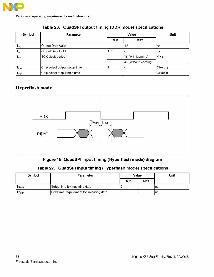
Table 26. QuadSPI output timing (DDR mode) specifications
Symbol Parameter Value Unit
Min Max
Tov Output Data Valid - 4.5 ns
Toh Output Data Hold 1.5 - ns
Tck SCK clock period - 75 (with learning) MHz
- 45 (without learning)
Tcss Chip select output setup time 2 - Clk(sck)
Tcsh Chip select output hold time -1 - Clk(sck)
Hyperflash mode
TsMIN
RDS
DI[7:0]
ThMIN
Figure 18. QuadSPI input timing (Hyperflash mode) diagram
Table 27. QuadSPI input timing (Hyperflash mode) specifications
Symbol Parameter Value Unit
Min Max
TsMIN Setup time for incoming data 2 - ns
ThMIN Hold time requirement for incoming data 2 - ns
Peripheral operating requirements and behaviors
38 Kinetis K82 Sub-Family, Rev.1, 09/2015.
Freescale Semiconductor, Inc.

CK
CK 2
THO
TDVO
TclkSKMAX
TclkSKMIN
Output Invalid Data
Figure 19. QuadSPI output timing (Hyperflash mode) diagram
Table 28. QuadSPI output timing (Hyperflash mode) specifications
Symbol Parameter Value Unit
Min Max
TdvMAX Output Data Valid - 4.3 ns
Tho Output Data Hold 1.3 - ns
TclkSKMAX Ck to Ck2 skew max - T/4 + 0.5 ns
TclkSKMIN Ck to Ck2 skew min T/4 - 0.5 - ns
NOTEMaximum clock frequency = 75 MHz.
3.3.2 Flash electrical specifications
This section describes the electrical characteristics of the flash memory module.
3.3.2.1 Flash timing specifications — program and erase
The following specifications represent the amount of time the internal charge pumpsare active and do not include command overhead.
Table 29. NVM program/erase timing specifications
Symbol Description Min. Typ. Max. Unit Notes
thvpgm4 Longword Program high-voltage time — 7.5 18 μs —
Table continues on the next page...
Peripheral operating requirements and behaviors
Kinetis K82 Sub-Family, Rev.1, 09/2015. 39
Freescale Semiconductor, Inc.

Table 29. NVM program/erase timing specifications (continued)
Symbol Description Min. Typ. Max. Unit Notes
thversscr Sector Erase high-voltage time — 13 113 ms 1
thversall Erase All high-voltage time — 208 1808 ms 1
1. Maximum time based on expectations at cycling end-of-life.
3.3.2.2 Flash timing specifications — commandsTable 30. Flash command timing specifications
Symbol Description Min. Typ. Max. Unit Notes
trd1sec4k Read 1s Section execution time (flash sector) — — 60 μs 1
tpgmchk Program Check execution time — — 45 μs 1
trdrsrc Read Resource execution time — — 30 μs 1
tpgm4 Program Longword execution time — 65 145 μs —
tersscr Erase Flash Sector execution time — 14 114 ms 2
trd1all Read 1s All Blocks execution time — — 0.9 ms 1
trdonce Read Once execution time — — 30 μs 1
tpgmonce Program Once execution time — 100 — μs —
tersall Erase All Blocks execution time — 280 2100 ms 2
tvfykey Verify Backdoor Access Key execution time — — 30 μs 1
1. Assumes 25 MHz flash clock frequency.2. Maximum times for erase parameters based on expectations at cycling end-of-life.
3.3.2.3 Flash high voltage current behaviorsTable 31. Flash high voltage current behaviors
Symbol Description Min. Typ. Max. Unit
IDD_PGM Average current adder during high voltageflash programming operation
— 2.5 6.0 mA
IDD_ERS Average current adder during high voltageflash erase operation
— 1.5 4.0 mA
3.3.2.4 Reliability specificationsTable 32. NVM reliability specifications
Symbol Description Min. Typ.1 Max. Unit Notes
Program Flash
tnvmretp10k Data retention after up to 10 K cycles 5 50 — years —
Table continues on the next page...
Peripheral operating requirements and behaviors
40 Kinetis K82 Sub-Family, Rev.1, 09/2015.
Freescale Semiconductor, Inc.

Table 32. NVM reliability specifications (continued)
Symbol Description Min. Typ.1 Max. Unit Notes
tnvmretp1k Data retention after up to 1 K cycles 20 100 — years —
nnvmcycp Cycling endurance 10 K 50 K — cycles 2
1. Typical data retention values are based on measured response accelerated at high temperature and derated to aconstant 25 °C use profile. Engineering Bulletin EB618 does not apply to this technology. Typical endurance defined inEngineering Bulletin EB619.
2. Cycling endurance represents number of program/erase cycles at –40 °C ≤ Tj ≤ °C.
3.3.3 Flexbus switching specifications
All processor bus timings are synchronous; input setup/hold and output delay aregiven in respect to the rising edge of a reference clock, FB_CLK. The FB_CLKfrequency may be the same as the internal system bus frequency or an integer dividerof that frequency.
The following timing numbers indicate when data is latched or driven onto theexternal bus, relative to the Flexbus output clock (FB_CLK). All other timingrelationships can be derived from these values.
Table 33. Flexbus limited voltage range switching specifications
Num Description Min. Max. Unit Notes
Operating voltage 2.7 3.6 V
Frequency of operation — FB_CLK MHz
FB1 Clock period 1/FB_CLK — ns
FB2 Address, data, and control output valid — 11.8 ns
FB3 Address, data, and control output hold 1.0 — ns 1
FB4 Data and FB_TA input setup 6 — ns
FB5 Data and FB_TA input hold 0.0 — ns 2
1. Specification is valid for all FB_AD[31:0], FB_BE/BWEn, FB_CSn, FB_OE, FB_R/W,FB_TBST, FB_TSIZ[1:0],FB_ALE, and FB_TS.
2. Specification is valid for all FB_AD[31:0] and FB_TA.
Table 34. Flexbus full voltage range switching specifications
Num Description Min. Max. Unit Notes
Operating voltage 1.71 3.6 V
Frequency of operation — FB_CLK MHz
FB1 Clock period 1/FB_CLK — ns
FB2 Address, data, and control output valid — 12.6 ns
Table continues on the next page...
Peripheral operating requirements and behaviors
Kinetis K82 Sub-Family, Rev.1, 09/2015. 41
Freescale Semiconductor, Inc.

Table 34. Flexbus full voltage range switching specifications (continued)
Num Description Min. Max. Unit Notes
FB3 Address, data, and control output hold 1.0 — ns 1
FB4 Data and FB_TA input setup 12.5 — ns
FB5 Data and FB_TA input hold 0 — ns 2
1. Specification is valid for all FB_AD[31:0], FB_BE/BWEn, FB_CSn, FB_OE, FB_R/W,FB_TBST, FB_TSIZ[1:0], FB_ALE,and FB_TS.
2. Specification is valid for all FB_AD[31:0] and FB_TA.
Address
Address Data
TSIZ
AA=1
AA=0
AA=1
AA=0
FB1
FB3FB5
FB4
FB4
FB5
FB2
FB_CLK
FB_A[Y]
FB_D[X]
FB_RW
FB_TS
FB_ALE
FB_CSn
FB_OEn
FB_BEn
FB_TA
FB_TSIZ[1:0]
Figure 20. FlexBus read timing diagram
Peripheral operating requirements and behaviors
42 Kinetis K82 Sub-Family, Rev.1, 09/2015.
Freescale Semiconductor, Inc.

Address
Address Data
TSIZ
AA=1
AA=0
AA=1
AA=0
FB1
FB3
FB4
FB5
FB2FB_CLK
FB_A[Y]
FB_D[X]
FB_RW
FB_TS
FB_ALE
FB_CSn
FB_OEn
FB_BEn
FB_TA
FB_TSIZ[1:0]
Figure 21. FlexBus write timing diagram
3.3.4 SDRAM controller specifications
Following figure shows SDRAM read cycle.
Peripheral operating requirements and behaviors
Kinetis K82 Sub-Family, Rev.1, 09/2015. 43
Freescale Semiconductor, Inc.
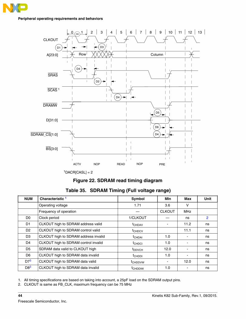
A[23:0]
SRAS
D[31:0]
ACTV NOP
SDRAM_CS[1:0]
READ
Column
CLKOUT
0
DRAMW
BS[3:0]
1 2 3 4 5 6 7 8 9 10 11 12 13
D1
D2
D4
D6
D5
D4
1
1
NOP
D4
Row
D3
PRE
D0
SCAS
DACR[CASL] = 2
Figure 22. SDRAM read timing diagram
Table 35. SDRAM Timing (Full voltage range)
NUM Characteristic 1 Symbol MIn Max Unit
Operating voltage 1.71 3.6 V
Frequency of operation — CLKOUT MHz
D0 Clock period 1/CLKOUT — ns 2
D1 CLKOUT high to SDRAM address valid tCHDAV - 11.2 ns
D2 CLKOUT high to SDRAM control valid tCHDCV 11.1 ns
D3 CLKOUT high to SDRAM address invalid tCHDAI 1.0 - ns
D4 CLKOUT high to SDRAM control invalid tCHDCI 1.0 - ns
D5 SDRAM data valid to CLKOUT high tDDVCH 12.0 - ns
D6 CLKOUT high to SDRAM data invalid tCHDDI 1.0 - ns
D73 CLKOUT high to SDRAM data valid tCHDDVW - 12.0 ns
D83 CLKOUT high to SDRAM data invalid tCHDDIW 1.0 - ns
1. All timing specifications are based on taking into account, a 25pF load on the SDRAM output pins.2. CLKOUT is same as FB_CLK, maximum frequency can be 75 MHz
Peripheral operating requirements and behaviors
44 Kinetis K82 Sub-Family, Rev.1, 09/2015.
Freescale Semiconductor, Inc.

3. D7 and D8 are for write cycles only.
Table 36. SDRAM Timing (Limited voltage range)
NUM Characteristic 1 Symbol MIn Max Unit
Operating voltage 2.7 3.6 V
Frequency of operation — CLKOUT MHz
D0 Clock period 1/CLKOUT — ns 2
D1 CLKOUT high to SDRAM address valid tCHDAV - 11.1 ns
D2 CLKOUT high to SDRAM control valid tCHDCV 11.1 ns
D3 CLKOUT high to SDRAM address invalid tCHDAI 1.0 - ns
D4 CLKOUT high to SDRAM control invalid tCHDCI 1.0 - ns
D5 SDRAM data valid to CLKOUT high tDDVCH 7.3 - ns
D6 CLKOUT high to SDRAM data invalid tCHDDI 1.0 - ns
D73 CLKOUT high to SDRAM data valid tCHDDVW - 11.1 ns
D83 CLKOUT high to SDRAM data invalid tCHDDIW 1.0 - ns
1. All timing specifications are based on taking into account, a 25pF load on the SDRAM output pins.2. CLKOUT is same as FB_CLK, maximum frequency can be 75 MHz3. D7 and D8 are for write cycles only.
Following figure shows an SDRAM write cycle.
Peripheral operating requirements and behaviors
Kinetis K82 Sub-Family, Rev.1, 09/2015. 45
Freescale Semiconductor, Inc.

A[23:0]
SRAS
SCAS1
D[31:0]
ACTV PALLNOP
SDRAM_CS[1:0]
WRITE
Row Column
CLKOUT
DRAMW
BS[3:0]
D1
D2
D4
D8
D4
0 1 2 3 4 5 6 7 8 9 10 11 12
D7
NOP
1 DACR[CASL] = 2
D4
D3
D2
D4
D0
Figure 23. SDRAM write timing diagram
3.4 Security and integrity modules
There are no specifications necessary for the device's security and integrity modules.
3.5 Analog
3.5.1 ADC electrical specifications
The 16-bit accuracy specifications listed in Table 37 and Table 38 are achievable on thedifferential pins ADCx_DP0, ADCx_DM0.
Peripheral operating requirements and behaviors
46 Kinetis K82 Sub-Family, Rev.1, 09/2015.
Freescale Semiconductor, Inc.

All other ADC channels meet the 13-bit differential/12-bit single-ended accuracyspecifications.
3.5.1.1 ADC operating conditionsTable 37. ADC operating conditions
Symbol Description Conditions Min. Typ.1 Max. Unit Notes
VDDA Supply voltage Absolute 1.71 — 3.6 V
ΔVDDA Supply voltage Delta to VDD (VDD – VDDA) -100 0 +100 mV 2
ΔVSSA Ground voltage Delta to VSS (VSS – VSSA) -100 0 +100 mV 2
VREFH ADC referencevoltage high
1.13 VDDA VDDA V
VREFL ADC referencevoltage low
VSSA VSSA VSSA V
VADIN Input voltage • 16-bit differential mode
• All other modes
VREFL
VREFL
—
—
31/32 ×VREFH
VREFH
V
CADIN Inputcapacitance
• 8-bit / 10-bit / 12-bitmodes
— 4 5 pF
RADIN Input seriesresistance
— 2 5 kΩ
RAS Analog sourceresistance(external)
13-bit / 12-bit modes
fADCK < 4 MHz
—
—
5
kΩ
3
fADCK ADC conversionclock frequency
≤ 13-bit mode 1.0 — 18.0 MHz 4
Crate ADC conversionrate
≤ 13-bit modes
No ADC hardware averaging
Continuous conversionsenabled, subsequentconversion time
20.000
—
818.330
ksps
5
1. Typical values assume VDDA = 3.0 V, Temp = 25 °C, fADCK = 1.0 MHz, unless otherwise stated. Typical values are forreference only, and are not tested in production.
2. DC potential difference.3. This resistance is external to MCU. To achieve the best results, the analog source resistance must be kept as low as
possible. The results in this data sheet were derived from a system that had < 8 Ω analog source resistance. TheRAS/CAS time constant should be kept to < 1 ns.
4. To use the maximum ADC conversion clock frequency, CFG2[ADHSC] must be set and CFG1[ADLPC] must be clear.5. For guidelines and examples of conversion rate calculation, download the ADC calculator tool.
Peripheral operating requirements and behaviors
Kinetis K82 Sub-Family, Rev.1, 09/2015. 47
Freescale Semiconductor, Inc.

RAS
VAS CAS
ZAS
VADIN
ZADIN
RADIN
RADIN
RADIN
RADIN
CADIN
Pad leakagedue toinput protection
INPUT PIN
INPUT PIN
INPUT PIN
SIMPLIFIEDINPUT PIN EQUIVALENT
CIRCUITSIMPLIFIED
CHANNEL SELECTCIRCUIT ADC SAR
ENGINE
Figure 24. ADC input impedance equivalency diagram
3.5.1.2 ADC electrical characteristics
Table 38. ADC characteristics (VREFH = VDDA, VREFL = VSSA)
Symbol Description Conditions1 Min. Typ.2 Max. Unit Notes
IDDA_ADC Supply current 0.215 — 1.7 mA 3
fADACK
ADC asynchronousclock source
• ADLPC = 1, ADHSC = 0
• ADLPC = 1, ADHSC = 1
• ADLPC = 0, ADHSC = 0
• ADLPC = 0, ADHSC = 1
1.2
2.4
3.0
4.4
2.4
4.0
5.2
6.2
3.9
6.1
7.3
9.5
MHz
MHz
MHz
MHz
tADACK = 1/fADACK
Sample Time See Reference Manual chapter for sample times
TUE Total unadjustederror
• 12-bit modes
• <12-bit modes
—
—
±4
±1.4
±6.8
±2.1
LSB4 5
DNL Differential non-linearity
• 12-bit modes
• <12-bit modes
—
—
±0.7
±0.2
–1.1 to+1.9
–0.3 to0.5
LSB4 5
INL Integral non-linearity • 12-bit modes — ±1.0 –2.7 to+1.9
LSB4 5
Table continues on the next page...
Peripheral operating requirements and behaviors
48 Kinetis K82 Sub-Family, Rev.1, 09/2015.
Freescale Semiconductor, Inc.

Table 38. ADC characteristics (VREFH = VDDA, VREFL = VSSA) (continued)
Symbol Description Conditions1 Min. Typ.2 Max. Unit Notes
• <12-bit modes— ±0.5 –0.7 to
+0.5
EFS Full-scale error • 12-bit modes
• <12-bit modes
—
—
–4
–1.4
–5.4
–1.8
LSB4 VADIN = VDDA5
EQ Quantization error • ≤13-bit modes — — ±0.5 LSB4
ENOB Effective number ofbits
16-bit differential mode
• Avg = 32
• Avg = 4
16-bit single-ended mode
• Avg = 32
• Avg = 4
12.8
11.9
12.2
11.4
14.5
13.8
13.9
13.1
—
—
—
—
bits
bits
bits
bits
6
THD Total harmonicdistortion
16-bit differential mode
• Avg = 32
16-bit single-ended mode
• Avg = 32
—
—
-94
-85
—
—
dB
dB
7
SFDR Spurious freedynamic range
16-bit differential mode
• Avg = 32
16-bit single-ended mode
• Avg = 32
82
78
95
90
—
—
dB
dB
7
EIL Input leakage error IIn × RAS mV IIn = leakagecurrent
(refer to theMCU's voltage
and currentoperatingratings)
Temp sensor slope Across the full temperaturerange of the device
1.55 1.62 1.69 mV/°C 8
VTEMP25 Temp sensor voltage 25 °C 706 716 726 mV 8
1. All accuracy numbers assume the ADC is calibrated with VREFH = VDDA2. Typical values assume VDDA = 3.0 V, Temp = 25 °C, fADCK = 2.0 MHz unless otherwise stated. Typical values are for
reference only and are not tested in production.3. The ADC supply current depends on the ADC conversion clock speed, conversion rate and ADC_CFG1[ADLPC] (low
power). For lowest power operation, ADC_CFG1[ADLPC] must be set, the ADC_CFG2[ADHSC] bit must be clear with1 MHz ADC conversion clock speed.
4. 1 LSB = (VREFH - VREFL)/2N
5. ADC conversion clock < 16 MHz, Max hardware averaging (AVGE = %1, AVGS = %11)6. Input data is 100 Hz sine wave. ADC conversion clock < 12 MHz.7. Input data is 1 kHz sine wave. ADC conversion clock < 12 MHz.
Peripheral operating requirements and behaviors
Kinetis K82 Sub-Family, Rev.1, 09/2015. 49
Freescale Semiconductor, Inc.

8. ADC conversion clock < 3 MHz
Typical ADC 16-bit Differential ENOB vs ADC Clock100Hz, 90% FS Sine Input
ENO
B
ADC Clock Frequency (MHz)
15.00
14.70
14.40
14.10
13.80
13.50
13.20
12.90
12.60
12.30
12.001 2 3 4 5 6 7 8 9 10 1211
Hardware Averaging DisabledAveraging of 4 samplesAveraging of 8 samplesAveraging of 32 samples
Figure 25. Typical ENOB vs. ADC_CLK for 16-bit differential mode
3.5.2 CMP and 6-bit DAC electrical specificationsTable 39. Comparator and 6-bit DAC electrical specifications
Symbol Description Min. Typ. Max. Unit
VDD Supply voltage 1.71 — 3.6 V
IDDHS Supply current, High-speed mode (EN=1, PMODE=1) — — 200 μA
IDDLS Supply current, low-speed mode (EN=1, PMODE=0) — — 20 μA
VAIN Analog input voltage VSS – 0.3 — VDD V
VAIO Analog input offset voltage — — 20 mV
VH Analog comparator hysteresis1
• CR0[HYSTCTR] = 00
• CR0[HYSTCTR] = 01
• CR0[HYSTCTR] = 10
• CR0[HYSTCTR] = 11
—
—
—
—
5
10
20
30
—
—
—
—
mV
mV
mV
mV
VCMPOh Output high VDD – 0.5 — — V
VCMPOl Output low — — 0.5 V
tDHS Propagation delay, high-speed mode (EN=1, PMODE=1) 20 50 200 ns
tDLS Propagation delay, low-speed mode (EN=1, PMODE=0) 80 250 600 ns
Analog comparator initialization delay2 — — 40 μs
IDAC6b 6-bit DAC current adder (enabled) — 7 — μA
Table continues on the next page...
Peripheral operating requirements and behaviors
50 Kinetis K82 Sub-Family, Rev.1, 09/2015.
Freescale Semiconductor, Inc.
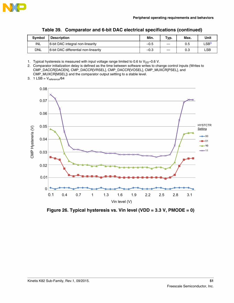
Table 39. Comparator and 6-bit DAC electrical specifications (continued)
Symbol Description Min. Typ. Max. Unit
INL 6-bit DAC integral non-linearity –0.5 — 0.5 LSB3
DNL 6-bit DAC differential non-linearity –0.3 — 0.3 LSB
1. Typical hysteresis is measured with input voltage range limited to 0.6 to VDD–0.6 V.2. Comparator initialization delay is defined as the time between software writes to change control inputs (Writes to
CMP_DACCR[DACEN], CMP_DACCR[VRSEL], CMP_DACCR[VOSEL], CMP_MUXCR[PSEL], andCMP_MUXCR[MSEL]) and the comparator output settling to a stable level.
3. 1 LSB = Vreference/64
00
01
10
HYSTCTR Setting
0.1
10
11
Vin level (V)
CM
P H
yste
reris
(V)
3.12.82.52.21.91.61.310.70.4
0.05
0
0.01
0.02
0.03
0.08
0.07
0.06
0.04
Figure 26. Typical hysteresis vs. Vin level (VDD = 3.3 V, PMODE = 0)
Peripheral operating requirements and behaviors
Kinetis K82 Sub-Family, Rev.1, 09/2015. 51
Freescale Semiconductor, Inc.

000110
HYSTCTR Setting
1011
0.1 3.12.82.52.21.91.61.310.70.4
0.1
0
0.02
0.04
0.06
0.18
0.14
0.12
0.08
0.16
Vin level (V)
CM
P H
yste
resi
s (V
)
Figure 27. Typical hysteresis vs. Vin level (VDD = 3.3 V, PMODE = 1)
3.5.3 12-bit DAC electrical characteristics
3.5.3.1 12-bit DAC operating requirementsTable 40. 12-bit DAC operating requirements
Symbol Desciption Min. Max. Unit Notes
VDDA Supply voltage 3.6 V
VDACR Reference voltage 1.13 3.6 V 1
CL Output load capacitance — 100 pF 2
IL Output load current — 1 mA
1. The DAC reference can be selected to be VDDA or VREFH.2. A small load capacitance (47 pF) can improve the bandwidth performance of the DAC.
Peripheral operating requirements and behaviors
52 Kinetis K82 Sub-Family, Rev.1, 09/2015.
Freescale Semiconductor, Inc.

3.5.3.2 12-bit DAC operating behaviorsTable 41. 12-bit DAC operating behaviors
Symbol Description Min. Typ. Max. Unit Notes
IDDA_DACL
P
Supply current — low-power mode — — 150 μA
IDDA_DACH
P
Supply current — high-speed mode — — 700 μA
tDACLP Full-scale settling time (0x080 to 0xF7F) —low-power mode
— 100 200 μs 1
tDACHP Full-scale settling time (0x080 to 0xF7F) —high-power mode
— 15 30 μs 1
tCCDACLP Code-to-code settling time (0xBF8 to0xC08) — low-power mode and high-speed mode
— 0.7 1 μs 1
Vdacoutl DAC output voltage range low — high-speed mode, no load, DAC set to 0x000
— — 100 mV
Vdacouth DAC output voltage range high — high-speed mode, no load, DAC set to 0xFFF
VDACR−100
— VDACR mV
INL Integral non-linearity error — high speedmode
— — ±8 LSB 2
DNL Differential non-linearity error — VDACR > 2V
— — ±1 LSB 3
DNL Differential non-linearity error — VDACR =VREF_OUT
— — ±1 LSB 4
VOFFSET Offset error — ±0.4 ±0.8 %FSR 5
EG Gain error — ±0.1 ±0.6 %FSR 5
PSRR Power supply rejection ratio, VDDA ≥ 2.4 V 60 — 90 dB
TCO Temperature coefficient offset voltage — 3.7 — μV/C 6
TGE Temperature coefficient gain error — 0.000421 — %FSR/C
AC Offset aging coefficient — — 100 μV/yr
Rop Output resistance (load = 3 kΩ) — — 250 Ω
SR Slew rate -80h→ F7Fh→ 80h
• High power (SPHP)
• Low power (SPLP)
1.2
0.05
1.7
0.12
—
—
V/μs
CT Channel to channel cross talk — — -80 dB
BW 3dB bandwidth
• High power (SPHP)
• Low power (SPLP)
550
40
—
—
—
—
kHz
1. Settling within ±1 LSB2. The INL is measured for 0 + 100 mV to VDACR −100 mV3. The DNL is measured for 0 + 100 mV to VDACR −100 mV4. The DNL is measured for 0 + 100 mV to VDACR −100 mV with VDDA > 2.4 V5. Calculated by a best fit curve from VSS + 100 mV to VDACR − 100 mV
Peripheral operating requirements and behaviors
Kinetis K82 Sub-Family, Rev.1, 09/2015. 53
Freescale Semiconductor, Inc.

6. VDDA = 3.0 V, reference select set for VDDA (DACx_CO:DACRFS = 1), high power mode (DACx_C0:LPEN = 0), DAC setto 0x800, temperature range is across the full range of the device
Digital Code
DAC
12 IN
L (L
SB)
0
500 1000 1500 2000 2500 3000 3500 4000
2
4
6
8
-2
-4
-6
-80
Figure 28. Typical INL error vs. digital code
Peripheral operating requirements and behaviors
54 Kinetis K82 Sub-Family, Rev.1, 09/2015.
Freescale Semiconductor, Inc.

Temperature °C
DAC
12 M
id L
evel
Cod
e Vo
ltage
25 55 85 105 125
1.499
-40
1.4985
1.498
1.4975
1.497
1.4965
1.496
Figure 29. Offset at half scale vs. temperature
3.5.4 Voltage reference electrical specifications
Table 42. VREF full-range operating requirements
Symbol Description Min. Max. Unit Notes
VDDA Supply voltage 3.6 V
TA Temperature Operating temperaturerange of the device
°C
CL Output load capacitance 100 nF 1, 2
1. CL must be connected to VREF_OUT if the VREF_OUT functionality is being used for either an internal or externalreference.
2. The load capacitance should not exceed +/-25% of the nominal specified CL value over the operating temperaturerange of the device.
Peripheral operating requirements and behaviors
Kinetis K82 Sub-Family, Rev.1, 09/2015. 55
Freescale Semiconductor, Inc.
Table 43. VREF full-range operating behaviors
Symbol Description Min. Typ. Max. Unit Notes
Vout Voltage reference output with factory trim atnominal VDDA and temperature=25C
1.1915 1.195 1.1977 V 1
Vout Voltage reference output — factory trim 1.1584 — 1.2376 V 1
Vout Voltage reference output — user trim 1.193 — 1.197 V 1
Vstep Voltage reference trim step — 0.5 — mV 1
Vtdrift Temperature drift (Vmax -Vmin across the fulltemperature range)
— — 80 mV 1
Ibg Bandgap only current — — 80 µA 1
Ilp Low-power buffer current — — 360 uA 1
Ihp High-power buffer current — — 1 mA 1
ΔVLOAD Load regulation
• current = ± 1.0 mA
—
200
—
µV 1, 2
Tstup Buffer startup time — — 100 µs
Tchop_osc_st
up
Internal bandgap start-up delay with choposcillator enabled
— — 35 ms —
Vvdrift Voltage drift (Vmax -Vmin across the full voltagerange)
— 2 — mV 1
1. See the chip's Reference Manual for the appropriate settings of the VREF Status and Control register.2. Load regulation voltage is the difference between the VREF_OUT voltage with no load vs. voltage with defined load
Table 44. VREF limited-range operating requirements
Symbol Description Min. Max. Unit Notes
TA Temperature 0 50 °C
Table 45. VREF limited-range operating behaviors
Symbol Description Min. Max. Unit Notes
Vout Voltage reference output with factory trim 1.173 1.225 V
3.6 Timers
See General switching specifications.
3.7 Communication interfaces
Peripheral operating requirements and behaviors
56 Kinetis K82 Sub-Family, Rev.1, 09/2015.
Freescale Semiconductor, Inc.

3.7.1 EMV SIM specifications
Each EMV SIM module interface consists of a total of five pins.
The interface is designed to be used with synchronous Smart cards, meaning the EMVSIM module provides the clock used by the Smart card. The clock frequency istypically 372 times the Tx/Rx data rate; however, the EMV SIM module can alsowork with CLK frequencies of 16 times the Tx/Rx data rate.
There is no timing relationship between the clock and the data. The clock that theEMV SIM module provides to the Smart card is used by the Smart card to recover theclock from the data in the same manner as standard UART data exchanges. All fivesignals of the EMV SIM module are asynchronous with each other.
There are no required timing relationships between signals in normal mode. The smartcard is initiated by the interface device; the Smart card responds with Answer toReset. Although the EMV SIM interface has no defined requirements, the ISO/IEC7816 defines reset and power-down sequences (for detailed information see ISO/IEC7816).
EMVSIMn_PD
EMVSIMn_RST
EMVSIMn_CLK
EMVSIMn_IO
EMVSIMn_VCCEN
SI7
SI8
SI9
SI10
Figure 30. EMV SIM Clock Timing Diagram
Peripheral operating requirements and behaviors
Kinetis K82 Sub-Family, Rev.1, 09/2015. 57
Freescale Semiconductor, Inc.

The following table defines the general timing requirements for the EMV SIMinterface.
Table 46. Timing Specifications, High Drive Strength
ID Parameter Symbol Min Max Unit
SI1
EMV SIM clock frequency (EMVSIMn_CLK)1 Sfreq 1 5 MHz
SI2
EMV SIM clock rise time (EMVSIMn_CLK)2 Srise — 0.09 × (1/Sfreq) ns
SI3
EMV SIM clock fall time (EMVSIMn_CLK)2 Sfall — 0.09 × (1/Sfreq) ns
SI4
EMV SIM input transition time (EMVSIMn_IO,EMVSIMn_PD)
Stran 20 25 ns
Si5
EMV SIM I/O rise time / fall time (EMVSIMn_IO)3 Tr/Tf — 1 ns
Si6
EMV SIM RST rise time / fall time (EMVSIMn_RST)4 Tr/Tf — 1 ns
1. 50% duty cycle clock,2. With C = 50 pF3. With Cin = 30 pF, Cout = 30 pF,4. With Cin = 30 pF,
3.7.1.1 EMV SIM Reset Sequences
Smart cards may have internal reset, or active low reset. The following subset describesthe reset sequences in these two cases.
3.7.1.1.1 Smart Cards with Internal ResetFollowing figure shows the reset sequence for Smart cards with internal reset. The resetsequence comprises the following steps:
• After power-up, the clock signal is enabled on EMVSIMn_CLK (time T0)• After 200 clock cycles, EMVSIMn_IO must be asserted.• The card must send a response on EMVSIMn_IO acknowledging the reset between
400–40000 clock cycles after T0.
Peripheral operating requirements and behaviors
58 Kinetis K82 Sub-Family, Rev.1, 09/2015.
Freescale Semiconductor, Inc.

EMVSIMn_CLK
EMVSIMn_IO
2
T0
RESPONSE
1
EMVSIMn_VCCEN
Figure 31. Internal Reset Card Reset Sequence
The following table defines the general timing requirements for the SIM interface.
Table 47. Timing Specifications, Internal Reset Card Reset Sequence
Ref Min Max Units
1 — 200 EMVSIMx_CLKclock cycles
2 400 40,000 EMVSIMx_CLKclock cycles
3.7.1.1.2 Smart Cards with Active Low ResetFollowing figure shows the reset sequence for Smart cards with active low reset. Thereset sequence comprises the following steps::
• After power-up, the clock signal is enabled on EMVSIMn_CLK (time T0)• After 200 clock cycles, EMVSIMn_IO must be asserted.• EMVSIMn_RST must remain low for at least 40,000 clock cycles after T0 (no
response is to be received on RX during those 40,000 clock cycles)• EMVSIMn_RST is asserted (at time T1)• EMVSIMn_RST must remain asserted for at least 40,000 clock cycles after T1,
and a response must be received on EMVSIMn_IO between 400 and 40,000 clockcycles after T1.
Peripheral operating requirements and behaviors
Kinetis K82 Sub-Family, Rev.1, 09/2015. 59
Freescale Semiconductor, Inc.

EMVSIMn_VCCEN
EMVSIMn_CLK
EMVSIMn_IO
2
T0
1 RESPONSE
EMVSIMn_RST
T1
33
Figure 32. Active-Low-Reset Smart Card Reset Sequence
The following table defines the general timing requirements for the EMVSIMinterface..
Table 48. Timing Specifications, Internal Reset Card Reset Sequence
Ref No Min Max Units
1 — 200 EMVSIMx_CLK clock cycles
2 400 40,000 EMVSIMx_CLK clock cycles
3 40,000 — EMVSIMx_CLK clock cycles
3.7.1.2 EMVSIM Power-Down SequenceFollowing figure shows the EMV SIM interface power-down AC timing diagram.Table49 table shows the timing requirements for parameters (SI7–SI10) shown in the figure.The power-down sequence for the EMV SIM interface is as follows:
• EMVSIMn_SIMPD port detects the removal of the Smart Card• EMVSIMn_RST is negated• EMVSIMn_CLK is negated• EMVSIM_IO is negated• EMVSIMx_VCCENy is negated
Each of the above steps requires one Frtcclk period (usually 32 kHz and selected bySIM_SOPT1[OSC32KSEL]). Power-down may be initiated by a Smart card removaldetection; or it may be launched by the processor.
Peripheral operating requirements and behaviors
60 Kinetis K82 Sub-Family, Rev.1, 09/2015.
Freescale Semiconductor, Inc.

EMVSIMn_PD
EMVSIMn_RST
EMVSIMn_CLK
EMVSIMn_IO
EMVSIMn_VCCEN
SI7
SI8
SI9
SI10
Figure 33. Smart Card Interface Power Down AC Timing
Table 49. Timing Requirements for Power-down Sequence
Ref No Parameter Symbol Min Max Units
SI7 EMVSIM reset to SIM clock stop Srst2clk 0.9 × 1/Frtcclk1
1.1 × 1/Frtcclk μs
SI8 EMVSIM reset to SIM Tx datalow
Srst2dat 1.8 × 1/Frtcclk
2.2 × 1/Frtcclk μs
SI9 EMVSIM reset to SIM voltageenable low
Srst2ven 2.7 × 1/Frtcclk
3.3 × 1/Frtcclk μs
SI10 EMVSIM presence detect toSIM reset low
Spd2rst 0.9 × 1/Frtcclk
1.1 × 1/Frtcclk μs
1. Frtcclk is ERCLK32K, and this clock must be enabled during the power down sequence.
NOTESame timing is also followed when auto power down isinitiated. See Reference Manual for reference.
Peripheral operating requirements and behaviors
Kinetis K82 Sub-Family, Rev.1, 09/2015. 61
Freescale Semiconductor, Inc.

3.7.2 USB VREG electrical specificationsTable 50. USB VREG electrical specifications
Symbol Description Min. Typ.1 Max. Unit Notes
VREGIN Input supply voltage 2.7 — 5.5 V
IDDon Quiescent current — Run mode, load currentequal zero, input supply (VREGIN) > 3.6 V
— 125 186 μA
IDDstby Quiescent current — Standby mode, loadcurrent equal zero
— 1.1 10 μA
IDDoff Quiescent current — Shutdown mode
• VREGIN = 5.0 V and temperature=25 °C
• Across operating voltage and temperature
—
—
650
—
—
4
nA
μA
ILOADrun Maximum load current — Run mode — — 120 mA
ILOADstby Maximum load current — Standby mode — — 1 mA
VReg33out Regulator output voltage — Input supply(VREGIN) > 3.6 V
• Run mode
• Standby mode
3
2.1
3.3
2.8
3.6
3.6
V
V
VReg33out Regulator output voltage — Input supply(VREGIN) < 3.6 V, pass-through mode
2.1 — 3.6 V 2
COUT External output capacitor 1.76 2.2 8.16 μF
ESR External output capacitor equivalent seriesresistance
1 — 100 mΩ
ILIM Short circuit current — 290 — mA
1. Typical values assume VREGIN = 5.0 V, Temp = 25 °C unless otherwise stated.2. Operating in pass-through mode: regulator output voltage equal to the input voltage minus a drop proportional to ILoad.
3.7.3 USB DCD electrical specificationsTable 51. USB DCD electrical specifications
Symbol Description Min. Typ. Max. Unit
VDP_SRC,VDM_SRC
USB_DP and USB_DM source voltages (up to 250μA)
0.5 — 0.7 V
VLGC Threshold voltage for logic high 0.8 — 2.0 V
IDP_SRC USB_DP source current 7 10 13 μA
IDM_SINK,IDP_SINK
USB_DM and USB_DP sink currents 50 100 150 μA
RDM_DWN D- pulldown resistance for data pin contact detect 14.25 — 24.8 kΩ
VDAT_REF Data detect voltage 0.25 0.33 0.4 V
Peripheral operating requirements and behaviors
62 Kinetis K82 Sub-Family, Rev.1, 09/2015.
Freescale Semiconductor, Inc.

3.7.4 DSPI switching specifications (limited voltage range)
The DMA Serial Peripheral Interface (DSPI) provides a synchronous serial bus withmaster and slave operations. Many of the transfer attributes are programmable. Thetables below provide DSPI timing characteristics for classic SPI timing modes. Referto the DSPI chapter of the Reference Manual for information on the modified transferformats used for communicating with slower peripheral devices.
Table 52. Master mode DSPI timing (limited voltage range)
Num Description Min. Max. Unit Notes
Operating voltage 2.7 3.6 V
Frequency of operation — 30 MHz
DS1 DSPI_SCK output cycle time 2 x tBUS — ns
DS2 DSPI_SCK output high/low time (tSCK/2) − 2 (tSCK/2) + 2 ns
DS3 DSPI_PCSn valid to DSPI_SCK delay (tBUS x 2) −2
— ns 1
DS4 DSPI_SCK to DSPI_PCSn invalid delay (tBUS x 2) −2
— ns 2
DS5 DSPI_SCK to DSPI_SOUT valid — 15.0 ns
DS6 DSPI_SCK to DSPI_SOUT invalid 1.0 — ns
DS7 DSPI_SIN to DSPI_SCK input setup 15.8 — ns
DS8 DSPI_SCK to DSPI_SIN input hold 0 — ns
1. The delay is programmable in SPIx_CTARn[PSSCK] and SPIx_CTARn[CSSCK].2. The delay is programmable in SPIx_CTARn[PASC] and SPIx_CTARn[ASC].
DS3 DS4DS1DS2
DS7DS8
First data Last dataDS5
First data Data Last data
DS6
Data
DSPI_PCSn
DSPI_SCK
(CPOL=0)
DSPI_SIN
DSPI_SOUT
Figure 34. DSPI classic SPI timing — master mode
Peripheral operating requirements and behaviors
Kinetis K82 Sub-Family, Rev.1, 09/2015. 63
Freescale Semiconductor, Inc.

Table 53. Slave mode DSPI timing (limited voltage range)
Num Description Min. Max. Unit
Operating voltage 2.7 3.6 V
Frequency of operation 15 1 MHz
DS9 DSPI_SCK input cycle time 4 x tBUS — ns
DS10 DSPI_SCK input high/low time (tSCK/2) − 2 (tSCK/2) + 2 ns
DS11 DSPI_SCK to DSPI_SOUT valid — 23.0 ns
DS12 DSPI_SCK to DSPI_SOUT invalid 0 — ns
DS13 DSPI_SIN to DSPI_SCK input setup 2.7 — ns
DS14 DSPI_SCK to DSPI_SIN input hold 7.0 — ns
DS15 DSPI_SS active to DSPI_SOUT driven — 13 ns
DS16 DSPI_SS inactive to DSPI_SOUT not driven — 13 ns
1. The maximum operating frequency is measured with non-continuous CS and SCK. When DSPI is configured withcontinuous CS and SCK, there is a constraint that SPI clock should not be greater than 1/6 of bus clock, for example,when bus clock is 60MHz, SPI clock should not be greater than 10MHz.
First data Last data
First data Data Last data
Data
DS15
DS10 DS9
DS16DS11DS12
DS14DS13
DSPI_SS
DSPI_SCK
(CPOL=0)
DSPI_SOUT
DSPI_SIN
Figure 35. DSPI classic SPI timing — slave mode
Peripheral operating requirements and behaviors
64 Kinetis K82 Sub-Family, Rev.1, 09/2015.
Freescale Semiconductor, Inc.

3.7.5 DSPI switching specifications (full voltage range)
The DMA Serial Peripheral Interface (DSPI) provides a synchronous serial bus withmaster and slave operations. Many of the transfer attributes are programmable. Thetables below provides DSPI timing characteristics for classic SPI timing modes. Referto the DSPI chapter of the Reference Manual for information on the modified transferformats used for communicating with slower peripheral devices.
Table 54. Master mode DSPI timing (full voltage range)
Num Description Min. Max. Unit Notes
Operating voltage 1.71 3.6 V 1
Frequency of operation — 15 MHz
DS1 DSPI_SCK output cycle time 4 x tBUS — ns
DS2 DSPI_SCK output high/low time (tSCK/2) - 4 (tSCK/2) + 4 ns
DS3 DSPI_PCSn valid to DSPI_SCK delay (tBUS x 2) −4
— ns 2
DS4 DSPI_SCK to DSPI_PCSn invalid delay (tBUS x 2) −4
— ns 3
DS5 DSPI_SCK to DSPI_SOUT valid — 16 ns
DS6 DSPI_SCK to DSPI_SOUT invalid 1.0 — ns
DS7 DSPI_SIN to DSPI_SCK input setup 19.1 — ns
DS8 DSPI_SCK to DSPI_SIN input hold 0 — ns
1. The DSPI module can operate across the entire operating voltage for the processor, but to run across the full voltagerange the maximum frequency of operation is reduced.
2. The delay is programmable in SPIx_CTARn[PSSCK] and SPIx_CTARn[CSSCK].3. The delay is programmable in SPIx_CTARn[PASC] and SPIx_CTARn[ASC].
DS3 DS4DS1DS2
DS7DS8
First data Last dataDS5
First data Data Last data
DS6
Data
DSPI_PCSn
DSPI_SCK
(CPOL=0)
DSPI_SIN
DSPI_SOUT
Figure 36. DSPI classic SPI timing — master mode
Table 55. Slave mode DSPI timing (full voltage range)
Num Description Min. Max. Unit
Operating voltage 1.71 3.6 V
Table continues on the next page...
Peripheral operating requirements and behaviors
Kinetis K82 Sub-Family, Rev.1, 09/2015. 65
Freescale Semiconductor, Inc.

Table 55. Slave mode DSPI timing (full voltage range) (continued)
Num Description Min. Max. Unit
Frequency of operation — 7.5 MHz
DS9 DSPI_SCK input cycle time 8 x tBUS — ns
DS10 DSPI_SCK input high/low time (tSCK/2) - 4 (tSCK/2) + 4 ns
DS11 DSPI_SCK to DSPI_SOUT valid — 23.1 ns
DS12 DSPI_SCK to DSPI_SOUT invalid 0 — ns
DS13 DSPI_SIN to DSPI_SCK input setup 2.6 — ns
DS14 DSPI_SCK to DSPI_SIN input hold 7.0 — ns
DS15 DSPI_SS active to DSPI_SOUT driven — 13.0 ns
DS16 DSPI_SS inactive to DSPI_SOUT not driven — 13.0 ns
First data Last data
First data Data Last data
Data
DS15
DS10 DS9
DS16DS11DS12
DS14DS13
DSPI_SS
DSPI_SCK
(CPOL=0)
DSPI_SOUT
DSPI_SIN
Figure 37. DSPI classic SPI timing — slave mode
3.7.6 I2C switching specifications
See General switching specifications.
3.7.7 UART switching specifications
See General switching specifications.
3.7.8 LPUART switching specifications
See General switching specifications.
Peripheral operating requirements and behaviors
66 Kinetis K82 Sub-Family, Rev.1, 09/2015.
Freescale Semiconductor, Inc.
3.7.9 SDHC specifications
The following timing specs are defined at the chip I/O pin and must be translatedappropriately to arrive at timing specs/constraints for the physical interface.
Table 56. SDHC full voltage range switching specifications
Num Symbol Description Min. Max. Unit
Operating voltage 1.71 3.6 V
Card input clock
SD1 fpp Clock frequency (low speed) 0 400 kHz
fpp Clock frequency (SD\SDIO full speed\high speed) 0 25/45 MHz
fpp Clock frequency (MMC full speed\high speed) 0 25/45 MHz
fOD Clock frequency (identification mode) 0 400 kHz
SD2 tWL Clock low time 7 — ns
SD3 tWH Clock high time 7 — ns
SD4 tTLH Clock rise time — 3 ns
SD5 tTHL Clock fall time — 3 ns
SDHC output / card inputs SDHC_CMD, SDHC_DAT (reference to SDHC_CLK)
SD6 tOD SDHC output delay (output valid) 0 8.1 ns
SDHC input / card inputs SDHC_CMD, SDHC_DAT (reference to SDHC_CLK)
SD7 tISU SDHC input setup time 5 — ns
SD8 tIH SDHC input hold time 0 — ns
Table 57. SDHC limited voltage range switching specifications
Num Symbol Description Min. Max. Unit
Operating voltage 2.7 3.6 V
Card input clock
SD1 fpp Clock frequency (low speed) 0 400 kHz
fpp Clock frequency (SD\SDIO full speed\high speed) 0 25\50 MHz
fpp Clock frequency (MMC full speed\high speed) 0 20\50 MHz
fOD Clock frequency (identification mode) 0 400 kHz
SD2 tWL Clock low time 7 — ns
SD3 tWH Clock high time 7 — ns
SD4 tTLH Clock rise time — 3 ns
SD5 tTHL Clock fall time — 3 ns
SDHC output / card inputs SDHC_CMD, SDHC_DAT (reference to SDHC_CLK)
SD6 tOD SDHC output delay (output valid) 0 7 ns
SDHC input / card inputs SDHC_CMD, SDHC_DAT (reference to SDHC_CLK)
Table continues on the next page...
Peripheral operating requirements and behaviors
Kinetis K82 Sub-Family, Rev.1, 09/2015. 67
Freescale Semiconductor, Inc.

Table 57. SDHC limited voltage range switching specifications (continued)
Num Symbol Description Min. Max. Unit
SD7 tISU SDHC input setup time 5 — ns
SD8 tIH SDHC input hold time 0 — ns
SD2SD3 SD1
SD6
SD8SD7
SDHC_CLK
Output SDHC_CMD
Output SDHC_DAT[3:0]
Input SDHC_CMD
Input SDHC_DAT[3:0]
Figure 38. SDHC timing
3.7.10 I2S switching specifications
This section provides the AC timings for the I2S in master (clocks driven) and slavemodes (clocks input). All timings are given for non-inverted serial clock polarity(TCR[TSCKP] = 0, RCR[RSCKP] = 0) and a non-inverted frame sync (TCR[TFSI] = 0,RCR[RFSI] = 0). If the polarity of the clock and/or the frame sync have been inverted,all the timings remain valid by inverting the clock signal (I2S_BCLK) and/or the framesync (I2S_FS) shown in the figures below.
Table 58. I2S master mode timing (limited voltage range)
Num Description Min. Max. Unit
Operating voltage 2.7 3.6 V
S1 I2S_MCLK cycle time 40 — ns
S2 I2S_MCLK pulse width high/low 45% 55% MCLK period
S3 I2S_BCLK cycle time 80 — ns
S4 I2S_BCLK pulse width high/low 45% 55% BCLK period
S5 I2S_BCLK to I2S_FS output valid — 15 ns
S6 I2S_BCLK to I2S_FS output invalid 0 — ns
Table continues on the next page...
Peripheral operating requirements and behaviors
68 Kinetis K82 Sub-Family, Rev.1, 09/2015.
Freescale Semiconductor, Inc.

Table 58. I2S master mode timing (limited voltage range) (continued)
Num Description Min. Max. Unit
S7 I2S_BCLK to I2S_TXD valid — 15 ns
S8 I2S_BCLK to I2S_TXD invalid 0 — ns
S9 I2S_RXD/I2S_FS input setup before I2S_BCLK 15 — ns
S10 I2S_RXD/I2S_FS input hold after I2S_BCLK 0 — ns
S1 S2 S2
S3
S4S4
S5
S9
S7
S9 S10
S7
S8
S6
S10
S8
I2S_MCLK (output)
I2S_BCLK (output)
I2S_FS (output)
I2S_FS (input)
I2S_TXD
I2S_RXD
Figure 39. I2S timing — master mode
Table 59. I2S slave mode timing (limited voltage range)
Num Description Min. Max. Unit
Operating voltage 2.7 3.6 V
S11 I2S_BCLK cycle time (input) 80 — ns
S12 I2S_BCLK pulse width high/low (input) 45% 55% MCLK period
S13 I2S_FS input setup before I2S_BCLK 4.5 — ns
S14 I2S_FS input hold after I2S_BCLK 2 — ns
S15 I2S_BCLK to I2S_TXD/I2S_FS output valid — 20 ns
S16 I2S_BCLK to I2S_TXD/I2S_FS output invalid 0 — ns
S17 I2S_RXD setup before I2S_BCLK 4.5 — ns
S18 I2S_RXD hold after I2S_BCLK 2 — ns
S19 I2S_TX_FS input assertion to I2S_TXD output valid1 25 ns
1. Applies to first bit in each frame and only if the TCR4[FSE] bit is clear
Peripheral operating requirements and behaviors
Kinetis K82 Sub-Family, Rev.1, 09/2015. 69
Freescale Semiconductor, Inc.

S15
S13
S15
S17 S18
S15
S16
S16
S14
S16
S11
S12
S12
I2S_BCLK (input)
I2S_FS (output)
I2S_FS (input)
I2S_TXD
I2S_RXD
S19
Figure 40. I2S timing — slave modes
3.7.10.1 Normal Run, Wait and Stop mode performance over the fulloperating voltage range
This section provides the operating performance over the full operating voltage for thedevice in Normal Run, Wait and Stop modes.
Table 60. I2S/SAI master mode timing
Num. Characteristic Min. Max. Unit
Operating voltage 1.71 3.6 V
S1 I2S_MCLK cycle time 40 — ns
S2 I2S_MCLK (as an input) pulse width high/low 45% 55% MCLK period
S3 I2S_TX_BCLK/I2S_RX_BCLK cycle time (output) 80 — ns
S4 I2S_TX_BCLK/I2S_RX_BCLK pulse width high/low 45% 55% BCLK period
S5 I2S_TX_BCLK/I2S_RX_BCLK to I2S_TX_FS/I2S_RX_FS output valid
— 15 ns
S6 I2S_TX_BCLK/I2S_RX_BCLK to I2S_TX_FS/I2S_RX_FS output invalid
0 — ns
S7 I2S_TX_BCLK to I2S_TXD valid — 15 ns
S8 I2S_TX_BCLK to I2S_TXD invalid 0 — ns
S9 I2S_RXD/I2S_RX_FS input setup beforeI2S_RX_BCLK
15 — ns
S10 I2S_RXD/I2S_RX_FS input hold after I2S_RX_BCLK 0 — ns
Peripheral operating requirements and behaviors
70 Kinetis K82 Sub-Family, Rev.1, 09/2015.
Freescale Semiconductor, Inc.

S1 S2 S2
S3
S4S4
S5
S9
S7
S9 S10
S7
S8
S6
S10
S8
I2S_MCLK (output)
I2S_TX_BCLK/ I2S_RX_BCLK (output)
I2S_TX_FS/ I2S_RX_FS (output)
I2S_TX_FS/ I2S_RX_FS (input)
I2S_TXD
I2S_RXD
Figure 41. I2S/SAI timing — master modes
Table 61. I2S/SAI slave mode timing
Num. Characteristic Min. Max. Unit
Operating voltage 1.71 3.6 V
S11 I2S_TX_BCLK/I2S_RX_BCLK cycle time (input) 80 — ns
S12 I2S_TX_BCLK/I2S_RX_BCLK pulse width high/low(input)
45% 55% MCLK period
S13 I2S_TX_FS/I2S_RX_FS input setup beforeI2S_TX_BCLK/I2S_RX_BCLK
4.5 — ns
S14 I2S_TX_FS/I2S_RX_FS input hold afterI2S_TX_BCLK/I2S_RX_BCLK
2 — ns
S15 I2S_TX_BCLK to I2S_TXD/I2S_TX_FS output valid — 23.1 ns
S16 I2S_TX_BCLK to I2S_TXD/I2S_TX_FS outputinvalid
0 — ns
S17 I2S_RXD setup before I2S_RX_BCLK 4.5 — ns
S18 I2S_RXD hold after I2S_RX_BCLK 2 — ns
S19 I2S_TX_FS input assertion to I2S_TXD output valid1 — 25 ns
1. Applies to first bit in each frame and only if the TCR4[FSE] bit is clear
Peripheral operating requirements and behaviors
Kinetis K82 Sub-Family, Rev.1, 09/2015. 71
Freescale Semiconductor, Inc.

S15
S13
S15
S17 S18
S15
S16
S16
S14
S16
S11
S12S12
I2S_TX_BCLK/ I2S_RX_BCLK (input)
I2S_TX_FS/ I2S_RX_FS (output)
I2S_TXD
I2S_RXD
I2S_TX_FS/ I2S_RX_FS (input) S19
Figure 42. I2S/SAI timing — slave modes
3.7.10.2 VLPR, VLPW, and VLPS mode performance over the fulloperating voltage range
This section provides the operating performance over the full operating voltage for thedevice in VLPR, VLPW, and VLPS modes.
Table 62. I2S/SAI master mode timing in VLPR, VLPW, and VLPS modes(full voltage range)
Num. Characteristic Min. Max. Unit
Operating voltage 1.71 3.6 V
S1 I2S_MCLK cycle time 62.5 — ns
S2 I2S_MCLK pulse width high/low 45% 55% MCLK period
S3 I2S_TX_BCLK/I2S_RX_BCLK cycle time (output) 250 — ns
S4 I2S_TX_BCLK/I2S_RX_BCLK pulse width high/low 45% 55% BCLK period
S5 I2S_TX_BCLK/I2S_RX_BCLK to I2S_TX_FS/I2S_RX_FS output valid
— 45 ns
S6 I2S_TX_BCLK/I2S_RX_BCLK to I2S_TX_FS/I2S_RX_FS output invalid
0 — ns
S7 I2S_TX_BCLK to I2S_TXD valid — 45 ns
S8 I2S_TX_BCLK to I2S_TXD invalid 0 — ns
S9 I2S_RXD/I2S_RX_FS input setup beforeI2S_RX_BCLK
45 — ns
S10 I2S_RXD/I2S_RX_FS input hold after I2S_RX_BCLK 0 — ns
Peripheral operating requirements and behaviors
72 Kinetis K82 Sub-Family, Rev.1, 09/2015.
Freescale Semiconductor, Inc.

S1 S2 S2
S3
S4S4
S5
S9
S7
S9 S10
S7
S8
S6
S10
S8
I2S_MCLK (output)
I2S_TX_BCLK/ I2S_RX_BCLK (output)
I2S_TX_FS/ I2S_RX_FS (output)
I2S_TX_FS/ I2S_RX_FS (input)
I2S_TXD
I2S_RXD
Figure 43. I2S/SAI timing — master modes
Table 63. I2S/SAI slave mode timing in VLPR, VLPW, and VLPS modes (fullvoltage range)
Num. Characteristic Min. Max. Unit
Operating voltage 1.71 3.6 V
S11 I2S_TX_BCLK/I2S_RX_BCLK cycle time (input) 250 — ns
S12 I2S_TX_BCLK/I2S_RX_BCLK pulse width high/low(input)
45% 55% MCLK period
S13 I2S_TX_FS/I2S_RX_FS input setup beforeI2S_TX_BCLK/I2S_RX_BCLK
30 — ns
S14 I2S_TX_FS/I2S_RX_FS input hold afterI2S_TX_BCLK/I2S_RX_BCLK
5 — ns
S15 I2S_TX_BCLK to I2S_TXD/I2S_TX_FS output valid — 56.5 ns
S16 I2S_TX_BCLK to I2S_TXD/I2S_TX_FS outputinvalid
0 — ns
S17 I2S_RXD setup before I2S_RX_BCLK 30 — ns
S18 I2S_RXD hold after I2S_RX_BCLK 5 — ns
S19 I2S_TX_FS input assertion to I2S_TXD output valid1 — 72 ns
1. Applies to first bit in each frame and only if the TCR4[FSE] bit is clear
Peripheral operating requirements and behaviors
Kinetis K82 Sub-Family, Rev.1, 09/2015. 73
Freescale Semiconductor, Inc.

S15
S13
S15
S17 S18
S15
S16
S16
S14
S16
S11
S12S12
I2S_TX_BCLK/ I2S_RX_BCLK (input)
I2S_TX_FS/ I2S_RX_FS (output)
I2S_TXD
I2S_RXD
I2S_TX_FS/ I2S_RX_FS (input) S19
Figure 44. I2S/SAI timing — slave modes
3.8 Human-machine interfaces (HMI)
3.8.1 TSI electrical specificationsTable 64. TSI electrical specifications
Symbol Description Min. Typ. Max. Unit
TSI_RUNF Fixed power consumption in run mode — 100 — µA
TSI_RUNV Variable power consumption in run mode(depends on oscillator's current selection)
1.0 — 128 µA
TSI_EN Power consumption in enable mode — 100 — µA
TSI_DIS Power consumption in disable mode — 1.2 — µA
TSI_TEN TSI analog enable time — 66 — µs
TSI_CREF TSI reference capacitor — 1.0 — pF
TSI_DVOLT Voltage variation of VP & VM around nominalvalues
0.19 — 1.03 V
4 Dimensions
4.1 Obtaining package dimensions
Package dimensions are provided in package drawings.
Dimensions
74 Kinetis K82 Sub-Family, Rev.1, 09/2015.
Freescale Semiconductor, Inc.

To find a package drawing, go to freescale.com and perform a keyword search for thedrawing’s document number:
If you want the drawing for this package Then use this document number
100-pin LQFP 98ASS23308W
121-pin XFBGA 98ASA00595D
144-pin LQFP 98ASS23177W1
1. The 144-pin LQFP package for this product is not yet available, however it is included in a Package Your Wayprogram for Kinetis MCUs. Visit freescale.com/KPYW for more details.
5 Pinout
5.1 K82 Signal Multiplexing and Pin Assignments
The following table shows the signals available on each pin and the locations of thesepins on the devices supported by this document. The Port Control Module isresponsible for selecting which ALT functionality is available on each pin.
NOTEThe 144-pin LQFP and 121-WLCSP packages for thisproduct are not yet available, however they are included in aPackage Your Way program for Kinetis MCUs. Visitfreescale.com/KPYW for more details.
144LQFP
100LQFP
121XFBGA
121WLCSP
Pin Name Default ALT0 ALT1 ALT2 ALT3 ALT4 ALT5 ALT6 ALT7 QSPI_SIP_MODE
x — H6 K9 NC NC NC
— — — G8 ADC0_SE16
ADC0_SE16
ADC0_SE16
— — A11 — NC NC NC
— — J6 — NC NC NC
— — J4 — NC NC NC
1 1 B1 C10 PTE0 DISABLED PTE0 SPI1_PCS1
LPUART1_TX
SDHC0_D1 QSPI0A_DATA3
I2C1_SDA RTC_CLKOUT
2 2 C2 D9 PTE1/LLWU_P0
DISABLED PTE1/LLWU_P0
SPI1_SCK LPUART1_RX
SDHC0_D0 QSPI0A_SCLK
I2C1_SCL SPI1_SIN
3 3 C1 D10 PTE2/LLWU_P1
DISABLED PTE2/LLWU_P1
SPI1_SOUT
LPUART1_CTS_b
SDHC0_DCLK
QSPI0A_DATA0
SPI1_SCK
4 4 D2 B11 PTE3 DISABLED PTE3 SPI1_PCS2
LPUART1_RTS_b
SDHC0_CMD
QSPI0A_DATA2
SPI1_SOUT
Pinout
Kinetis K82 Sub-Family, Rev.1, 09/2015. 75
Freescale Semiconductor, Inc.

144LQFP
100LQFP
121XFBGA
121WLCSP
Pin Name Default ALT0 ALT1 ALT2 ALT3 ALT4 ALT5 ALT6 ALT7 QSPI_SIP_MODE
5 5 F7 F6 VSS VSS VSS
6 6 E5 F7 VDDIO_E VDDIO_E VDDIO_E
7 7 D1 C11 PTE4/LLWU_P2
DISABLED PTE4/LLWU_P2
SPI1_SIN LPUART3_TX
SDHC0_D3 QSPI0A_DATA1
8 8 E2 E8 PTE5 DISABLED PTE5 SPI1_PCS0
LPUART3_RX
SDHC0_D2 QSPI0A_SS0_B
FTM3_CH0 USB0_SOF_OUT
9 9 E1 E9 PTE6/LLWU_P16
DISABLED PTE6/LLWU_P16
SPI1_PCS3
LPUART3_CTS_b
I2S0_MCLK
QSPI0B_DATA3
FTM3_CH1 SDHC0_D4
10 10 F3 E10 PTE7 DISABLED PTE7 SPI2_SCK LPUART3_RTS_b
I2S0_RXD0 QSPI0B_SCLK
FTM3_CH2 QSPI0A_SS1_B
11 11 F2 D11 PTE8 DISABLED PTE8 I2S0_RXD1 SPI2_SOUT
I2S0_RX_FS
QSPI0B_DATA0
FTM3_CH3 SDHC0_D5
12 12 F1 E11 PTE9/LLWU_P17
DISABLED PTE9/LLWU_P17
I2S0_TXD1 SPI2_PCS1
I2S0_RX_BCLK
QSPI0B_DATA2
FTM3_CH4 SDHC0_D6
13 13 G2 F8 PTE10/LLWU_P18
DISABLED PTE10/LLWU_P18
I2C3_SDA SPI2_SIN I2S0_TXD0 QSPI0B_DATA1
FTM3_CH5 SDHC0_D7
14 14 G1 F9 PTE11 DISABLED PTE11 I2C3_SCL SPI2_PCS0
I2S0_TX_FS
QSPI0B_SS0_B
FTM3_CH6 QSPI0A_DQS
15 — — — PTE12 DISABLED PTE12 LPUART2_TX
I2S0_TX_BCLK
QSPI0B_DQS
FTM3_CH7 FXIO0_D2 QSPI0A_DATA3
16 — — — PTE13 DISABLED PTE13 LPUART2_RX
QSPI0B_SS1_B
SDHC0_CLKIN
FXIO0_D3 QSPI0A_SCLK
17 15 — F10 VDDIO_E VDDIO_E VDDIO_E
18 16 — F11 VSS VSS VSS
19 — — — PTE16 ADC0_SE4a
ADC0_SE4a
PTE16 SPI0_PCS0
LPUART2_TX
FTM_CLKIN0
FTM0_FLT3
FXIO0_D4 QSPI0A_DATA0
20 — — — PTE17/LLWU_P19
ADC0_SE5a
ADC0_SE5a
PTE17/LLWU_P19
SPI0_SCK LPUART2_RX
FTM_CLKIN1
LPTMR0_ALT3/LPTMR1_ALT3
FXIO0_D5 QSPI0A_DATA2
21 — — — PTE18/LLWU_P20
ADC0_SE6a
ADC0_SE6a
PTE18/LLWU_P20
SPI0_SOUT
LPUART2_CTS_b
I2C0_SDA FXIO0_D6 QSPI0A_DATA1
22 — — — PTE19 ADC0_SE7a
ADC0_SE7a
PTE19 SPI0_SIN LPUART2_RTS_b
I2C0_SCL FXIO0_D7 QSPI0A_SS0_B
23 16 H3 F11 VSS VSS VSS
24 17 H2 G11 USB0_DP USB0_DP USB0_DP
25 18 H1 H11 USB0_DM USB0_DM USB0_DM
26 19 J1 G10 VOUT33 VOUT33 VOUT33
27 20 J2 H10 VREGIN VREGIN VREGIN
28 21 — G9 NC NC NC
29 — K2 J10 ADC0_DP0 ADC0_DP0 ADC0_DP0
30 — K1 K10 ADC0_DM0
ADC0_DM0
ADC0_DM0
31 — J3 J11 ADC0_DP3 ADC0_DP3 ADC0_DP3
Pinout
76 Kinetis K82 Sub-Family, Rev.1, 09/2015.
Freescale Semiconductor, Inc.

144LQFP
100LQFP
121XFBGA
121WLCSP
Pin Name Default ALT0 ALT1 ALT2 ALT3 ALT4 ALT5 ALT6 ALT7 QSPI_SIP_MODE
32 — K3 K11 ADC0_DM3
ADC0_DM3
ADC0_DM3
33 22 F5 H8 VDDA VDDA VDDA
34 23 G5 H9 VREFH VREFH VREFH
35 24 G6 J9 VREFL VREFL VREFL
36 25 F6 J8 VSSA VSSA VSSA
37 26 L2 — ADC0_DP1 ADC0_DP1 ADC0_DP1
38 27 L1 — ADC0_DM1
ADC0_DM1
ADC0_DM1
39 28 L3 L11 VREF_OUT/CMP1_IN5/CMP0_IN5/ADC0_SE22
VREF_OUT/CMP1_IN5/CMP0_IN5/ADC0_SE22
VREF_OUT/CMP1_IN5/CMP0_IN5/ADC0_SE22
40 29 K4 L10 DAC0_OUT/CMP1_IN3/ADC0_SE23
DAC0_OUT/CMP1_IN3/ADC0_SE23
DAC0_OUT/CMP1_IN3/ADC0_SE23
42 30 K5 H7 RTC_WAKEUP_B
RTC_WAKEUP_B
RTC_WAKEUP_B
43 31 L4 L9 XTAL32 XTAL32 XTAL32
44 32 L5 L8 EXTAL32 EXTAL32 EXTAL32
45 33 K6 K8 VBAT VBAT VBAT
46 34 — G7 VDD VDD VDD
47 35 — F6 VSS VSS VSS
48 — H5 L7 PTA20 DISABLED PTA20 I2C0_SCL LPUART4_TX
FTM_CLKIN1
FXIO0_D8 EWM_OUT_b
TPM_CLKIN1
49 — J5 K7 PTA21/LLWU_P21
DISABLED PTA21/LLWU_P21
I2C0_SDA LPUART4_RX
FXIO0_D9 EWM_IN
50 36 L7 J7 PTA0 JTAG_TCLK/SWD_CLK
TSI0_CH1 PTA0 LPUART0_CTS_b
FTM0_CH5 FXIO0_D10 EMVSIM0_CLK
JTAG_TCLK/SWD_CLK
51 37 H8 J6 PTA1 JTAG_TDI TSI0_CH2 PTA1 LPUART0_RX
FTM0_CH6 I2C3_SDA FXIO0_D11 EMVSIM0_IO
JTAG_TDI
52 38 J7 K6 PTA2 JTAG_TDO/TRACE_SWO
TSI0_CH3 PTA2 LPUART0_TX
FTM0_CH7 I2C3_SCL FXIO0_D12 EMVSIM0_PD
JTAG_TDO/TRACE_SWO
53 39 H9 L6 PTA3 JTAG_TMS/SWD_DIO
TSI0_CH4 PTA3 LPUART0_RTS_b
FTM0_CH0 FXIO0_D13 EMVSIM0_RST
JTAG_TMS/SWD_DIO
54 40 J8 H6 PTA4/LLWU_P3
NMI_b TSI0_CH5 PTA4/LLWU_P3
FTM0_CH1 FXIO0_D14 EMVSIM0_VCCEN
NMI_b
Pinout
Kinetis K82 Sub-Family, Rev.1, 09/2015. 77
Freescale Semiconductor, Inc.

144LQFP
100LQFP
121XFBGA
121WLCSP
Pin Name Default ALT0 ALT1 ALT2 ALT3 ALT4 ALT5 ALT6 ALT7 QSPI_SIP_MODE
55 41 K7 H5 PTA5 DISABLED PTA5 USB0_CLKIN
FTM0_CH2 FXIO0_D15 I2S0_TX_BCLK
JTAG_TRST_b
56 — L10 G6 VDD VDD VDD
57 — K10 F5 VSS VSS VSS
58 — — — PTA6 DISABLED PTA6 I2C2_SCL FTM0_CH3 EMVSIM1_CLK
CLKOUT TRACE_CLKOUT
59 — — — PTA7 ADC0_SE10
ADC0_SE10
PTA7 I2C2_SDA FTM0_CH4 EMVSIM1_IO
TRACE_D3
60 — — — PTA8 ADC0_SE11
ADC0_SE11
PTA8 FTM1_CH0 EMVSIM1_PD
FTM1_QD_PHA/TPM1_CH0
TRACE_D2
61 — — — PTA9 DISABLED PTA9 FTM1_CH1 EMVSIM1_RST
FTM1_QD_PHB/TPM1_CH1
TRACE_D1
62 — J9 L5 PTA10/LLWU_P22
DISABLED PTA10/LLWU_P22
I2C2_SDA FTM2_CH0 EMVSIM1_VCCEN
FXIO0_D16 FTM2_QD_PHA/TPM2_CH0
TRACE_D0
63 — H7 L4 PTA11/LLWU_P23
DISABLED PTA11/LLWU_P23
I2C2_SCL FTM2_CH1 FXIO0_D17 FTM2_QD_PHB/TPM2_CH1
64 42 K8 K5 PTA12 DISABLED PTA12 FTM1_CH0 TRACE_CLKOUT
FXIO0_D18 I2S0_TXD0 FTM1_QD_PHA/TPM1_CH0
65 43 L8 J5 PTA13/LLWU_P4
DISABLED PTA13/LLWU_P4
FTM1_CH1 TRACE_D3 FXIO0_D19 I2S0_TX_FS
FTM1_QD_PHB/TPM1_CH1
66 44 K9 L3 PTA14 DISABLED PTA14 SPI0_PCS0
LPUART0_TX
TRACE_D2 FXIO0_D20 I2S0_RX_BCLK
I2S0_TXD1
67 45 L9 K4 PTA15 DISABLED PTA15 SPI0_SCK LPUART0_RX
TRACE_D1 FXIO0_D21 I2S0_RXD0
68 46 J10 J4 PTA16 DISABLED PTA16 SPI0_SOUT
LPUART0_CTS_b
TRACE_D0 FXIO0_D22 I2S0_RX_FS
I2S0_RXD1
69 47 H10 K3 PTA17 DISABLED PTA17 SPI0_SIN LPUART0_RTS_b
FXIO0_D23 I2S0_MCLK
70 48 E6 L2 VDD VDD VDD
71 49 G7 K2 VSS VSS VSS
72 50 L11 L1 PTA18 EXTAL0 EXTAL0 PTA18 FTM0_FLT2
FTM_CLKIN0
TPM_CLKIN0
73 51 K11 K1 PTA19 XTAL0 XTAL0 PTA19 FTM1_FLT0
FTM_CLKIN1
LPTMR0_ALT1/LPTMR1_ALT1
TPM_CLKIN1
74 52 J11 J1 RESET_b RESET_b RESET_b
75 — — — PTA24 DISABLED PTA24 EMVSIM0_CLK
FB_A29
Pinout
78 Kinetis K82 Sub-Family, Rev.1, 09/2015.
Freescale Semiconductor, Inc.

144LQFP
100LQFP
121XFBGA
121WLCSP
Pin Name Default ALT0 ALT1 ALT2 ALT3 ALT4 ALT5 ALT6 ALT7 QSPI_SIP_MODE
76 — — — PTA25 DISABLED PTA25 EMVSIM0_IO
FB_A28
77 — — — PTA26 DISABLED PTA26 EMVSIM0_PD
FB_A27
78 — — — PTA27 DISABLED PTA27 EMVSIM0_RST
FB_A26
79 — — — PTA28 DISABLED PTA28 EMVSIM0_VCCEN
FB_A25
80 — H11 J2 PTA29 DISABLED PTA29 FB_A24
81 53 G11 J3 PTB0/LLWU_P5
ADC0_SE8/TSI0_CH0
ADC0_SE8/TSI0_CH0
PTB0/LLWU_P5
I2C0_SCL FTM1_CH0 SDRAM_CAS_b
FTM1_QD_PHA/TPM1_CH0
FXIO0_D0
82 54 G10 H2 PTB1 ADC0_SE9/TSI0_CH6
ADC0_SE9/TSI0_CH6
PTB1 I2C0_SDA FTM1_CH1 SDRAM_RAS_b
FTM1_QD_PHB/TPM1_CH1
FXIO0_D1
83 55 G9 H1 PTB2 ADC0_SE12/TSI0_CH7
ADC0_SE12/TSI0_CH7
PTB2 I2C0_SCL LPUART0_RTS_b
SDRAM_WE
FTM0_FLT3
FXIO0_D2
84 56 G8 H3 PTB3 ADC0_SE13/TSI0_CH8
ADC0_SE13/TSI0_CH8
PTB3 I2C0_SDA LPUART0_CTS_b
SDRAM_CS0_b
FTM0_FLT0
FXIO0_D3
85 — B11 H4 PTB4 DISABLED PTB4 EMVSIM1_IO
SDRAM_CS1_b
FTM1_FLT0
86 — C11 G1 PTB5 DISABLED PTB5 EMVSIM1_CLK
FTM2_FLT0
87 — F11 G2 PTB6 DISABLED PTB6 EMVSIM1_VCCEN
FB_AD23/SDRAM_D23
88 — E11 G3 PTB7 DISABLED PTB7 EMVSIM1_PD
FB_AD22/SDRAM_D22
89 — D11 G4 PTB8 DISABLED PTB8 EMVSIM1_RST
LPUART3_RTS_b
FB_AD21/SDRAM_D21
90 57 E10 G5 PTB9 DISABLED PTB9 SPI1_PCS1
LPUART3_CTS_b
FB_AD20/SDRAM_D20
91 58 D10 F1 PTB10 DISABLED PTB10 SPI1_PCS0
LPUART3_RX
I2C2_SCL FB_AD19/SDRAM_D19
FTM0_FLT1
FXIO0_D4
92 59 C10 F2 PTB11 DISABLED PTB11 SPI1_SCK LPUART3_TX
I2C2_SDA FB_AD18/SDRAM_D18
FTM0_FLT2
FXIO0_D5
93 60 L6 F5 VSS VSS VSS
94 61 E7 G6 VDD VDD VDD
Pinout
Kinetis K82 Sub-Family, Rev.1, 09/2015. 79
Freescale Semiconductor, Inc.

144LQFP
100LQFP
121XFBGA
121WLCSP
Pin Name Default ALT0 ALT1 ALT2 ALT3 ALT4 ALT5 ALT6 ALT7 QSPI_SIP_MODE
95 62 B10 E1 PTB16 TSI0_CH9 TSI0_CH9 PTB16 SPI1_SOUT
LPUART0_RX
FTM_CLKIN0
FB_AD17/SDRAM_D17
EWM_IN TPM_CLKIN0
96 63 E9 F3 PTB17 TSI0_CH10 TSI0_CH10 PTB17 SPI1_SIN LPUART0_TX
FTM_CLKIN1
FB_AD16/SDRAM_D16
EWM_OUT_b
TPM_CLKIN1
97 64 D9 F4 PTB18 TSI0_CH11 TSI0_CH11 PTB18 FTM2_CH0 I2S0_TX_BCLK
FB_AD15/SDRAM_A23
FTM2_QD_PHA/TPM2_CH0
FXIO0_D6
98 65 C9 E2 PTB19 TSI0_CH12 TSI0_CH12 PTB19 FTM2_CH1 I2S0_TX_FS
FB_OE_b FTM2_QD_PHB/TPM2_CH1
FXIO0_D7
99 66 F10 D1 PTB20 DISABLED PTB20 SPI2_PCS0
FB_AD31/SDRAM_D31
CMP0_OUT
FXIO0_D8
100 67 F9 E3 PTB21 DISABLED PTB21 SPI2_SCK FB_AD30/SDRAM_D30
CMP1_OUT
FXIO0_D9
101 68 F8 E4 PTB22 DISABLED PTB22 SPI2_SOUT
FB_AD29/SDRAM_D29
FXIO0_D10
102 69 E8 D2 PTB23 DISABLED PTB23 SPI2_SIN SPI0_PCS5
FB_AD28/SDRAM_D28
FXIO0_D11
103 70 B9 C1 PTC0 ADC0_SE14/TSI0_CH13
ADC0_SE14/TSI0_CH13
PTC0 SPI0_PCS4
PDB0_EXTRG
USB0_SOF_OUT
FB_AD14/SDRAM_A22
I2S0_TXD1 FXIO0_D12
104 71 D8 D3 PTC1/LLWU_P6
ADC0_SE15/TSI0_CH14
ADC0_SE15/TSI0_CH14
PTC1/LLWU_P6
SPI0_PCS3
LPUART1_RTS_b
FTM0_CH0 FB_AD13/SDRAM_A21
I2S0_TXD0 FXIO0_D13
105 72 C8 C2 PTC2 ADC0_SE4b/CMP1_IN0/TSI0_CH15
ADC0_SE4b/CMP1_IN0/TSI0_CH15
PTC2 SPI0_PCS2
LPUART1_CTS_b
FTM0_CH1 FB_AD12/SDRAM_A20
I2S0_TX_FS
106 73 B8 B1 PTC3/LLWU_P7
CMP1_IN1 CMP1_IN1 PTC3/LLWU_P7
SPI0_PCS1
LPUART1_RX
FTM0_CH2 CLKOUT I2S0_TX_BCLK
107 74 — E5 VSS VSS VSS
108 75 — G6 VDD VDD VDD
109 76 A8 A1 PTC4/LLWU_P8
DISABLED PTC4/LLWU_P8
SPI0_PCS0
LPUART1_TX
FTM0_CH3 FB_AD11/SDRAM_A19
CMP1_OUT
110 77 D7 B2 PTC5/LLWU_P9
DISABLED PTC5/LLWU_P9
SPI0_SCK LPTMR0_ALT2/LPTMR1_ALT2
I2S0_RXD0 FB_AD10/SDRAM_A18
CMP0_OUT
FTM0_CH2
111 78 C7 C3 PTC6/LLWU_P10
CMP0_IN0 CMP0_IN0 PTC6/LLWU_P10
SPI0_SOUT
PDB0_EXTRG
I2S0_RX_BCLK
FB_AD9/SDRAM_A17
I2S0_MCLK
FXIO0_D14
Pinout
80 Kinetis K82 Sub-Family, Rev.1, 09/2015.
Freescale Semiconductor, Inc.

144LQFP
100LQFP
121XFBGA
121WLCSP
Pin Name Default ALT0 ALT1 ALT2 ALT3 ALT4 ALT5 ALT6 ALT7 QSPI_SIP_MODE
112 79 B7 A2 PTC7 CMP0_IN1 CMP0_IN1 PTC7 SPI0_SIN USB0_SOF_OUT
I2S0_RX_FS
FB_AD8/SDRAM_A16
FXIO0_D15
113 80 A7 B3 PTC8 CMP0_IN2 CMP0_IN2 PTC8 FTM3_CH4 I2S0_MCLK
FB_AD7/SDRAM_A15
FXIO0_D16
114 81 D6 D4 PTC9 CMP0_IN3 CMP0_IN3 PTC9 FTM3_CH5 I2S0_RX_BCLK
FB_AD6/SDRAM_A14
FTM2_FLT0
FXIO0_D17
115 82 C6 A3 PTC10 DISABLED PTC10 I2C1_SCL FTM3_CH6 I2S0_RX_FS
FB_AD5/SDRAM_A13
FXIO0_D18
116 83 C5 C4 PTC11/LLWU_P11
DISABLED PTC11/LLWU_P11
I2C1_SDA FTM3_CH7 I2S0_RXD1 FB_RW_b FXIO0_D19
117 84 B6 B4 PTC12 DISABLED PTC12 LPUART4_RTS_b
FTM_CLKIN0
FB_AD27/SDRAM_D27
FTM3_FLT0
TPM_CLKIN0
118 85 A6 A4 PTC13 DISABLED PTC13 LPUART4_CTS_b
FTM_CLKIN1
FB_AD26/SDRAM_D26
TPM_CLKIN1
119 86 A5 D5 PTC14 DISABLED PTC14 LPUART4_RX
FB_AD25/SDRAM_D25
FXIO0_D20
120 87 B5 C5 PTC15 DISABLED PTC15 LPUART4_TX
FB_AD24/SDRAM_D24
FXIO0_D21
121 88 — F6 VSS VSS VSS
122 89 — E6 VDD VDD VDD
123 — D5 A5 PTC16 DISABLED PTC16 LPUART3_RX
FB_CS5_b/FB_TSIZ1/FB_BE23_16_BLS15_8_b/SDRAM_DQM2
124 90 C4 B5 PTC17 DISABLED PTC17 LPUART3_TX
FB_CS4_b/FB_TSIZ0/FB_BE31_24_BLS7_0_b/SDRAM_DQM3
125 — B4 A6 PTC18 DISABLED PTC18 LPUART3_RTS_b
FB_TBST_b/FB_CS2_b/FB_BE15_8_BLS23_16_b/
Pinout
Kinetis K82 Sub-Family, Rev.1, 09/2015. 81
Freescale Semiconductor, Inc.

144LQFP
100LQFP
121XFBGA
121WLCSP
Pin Name Default ALT0 ALT1 ALT2 ALT3 ALT4 ALT5 ALT6 ALT7 QSPI_SIP_MODE
SDRAM_DQM1
126 — A4 B6 PTC19 DISABLED PTC19 LPUART3_CTS_b
FB_CS3_b/FB_BE7_0_BLS31_24_b/SDRAM_DQM0
FB_TA_b
127 91 D4 C6 PTD0/LLWU_P12
DISABLED PTD0/LLWU_P12
SPI0_PCS0
LPUART2_RTS_b
FTM3_CH0 FB_ALE/FB_CS1_b/FB_TS_b
FXIO0_D22
128 92 D3 D6 PTD1 ADC0_SE5b
ADC0_SE5b
PTD1 SPI0_SCK LPUART2_CTS_b
FTM3_CH1 FB_CS0_b FXIO0_D23
129 93 C3 D7 PTD2/LLWU_P13
DISABLED PTD2/LLWU_P13
SPI0_SOUT
LPUART2_RX
FTM3_CH2 FB_AD4/SDRAM_A12
I2C0_SCL
130 94 B3 A7 PTD3 DISABLED PTD3 SPI0_SIN LPUART2_TX
FTM3_CH3 FB_AD3/SDRAM_A11
I2C0_SDA
131 95 A3 B7 PTD4/LLWU_P14
DISABLED PTD4/LLWU_P14
SPI0_PCS1
LPUART0_RTS_b
FTM0_CH4 FB_AD2/SDRAM_A10
EWM_IN SPI1_PCS0
132 96 A2 C7 PTD5 ADC0_SE6b
ADC0_SE6b
PTD5 SPI0_PCS2
LPUART0_CTS_b
FTM0_CH5 FB_AD1/SDRAM_A9
EWM_OUT_b
SPI1_SCK
133 97 B2 A8 PTD6/LLWU_P15
ADC0_SE7b
ADC0_SE7b
PTD6/LLWU_P15
SPI0_PCS3
LPUART0_RX
FTM0_CH6 FB_AD0 FTM0_FLT0
SPI1_SOUT
134 98 — F6 VSS VSS VSS
135 99 — E7 VDD VDD VDD
136 100 A1 B8 PTD7 DISABLED PTD7 CMT_IRO LPUART0_TX
FTM0_CH7 SDRAM_CKE
FTM0_FLT1
SPI1_SIN
137 — A10 A9 PTD8/LLWU_P24
DISABLED PTD8/LLWU_P24
I2C0_SCL FB_A16 FXIO0_D24
138 — A9 C8 PTD9 DISABLED PTD9 I2C0_SDA FB_A17 FXIO0_D25
139 — E4 B9 PTD10 DISABLED PTD10 FB_A18 FXIO0_D26
140 — E3 A10 PTD11/LLWU_P25
DISABLED PTD11/LLWU_P25
SPI2_PCS0
FB_A19 FXIO0_D27
141 — F4 D8 PTD12 DISABLED PTD12 SPI2_SCK FTM3_FLT0
FB_A20 FXIO0_D28
142 — G3 C9 PTD13 DISABLED PTD13 SPI2_SOUT
FB_A21 FXIO0_D29
143 — G4 B10 PTD14 DISABLED PTD14 SPI2_SIN FB_A22 FXIO0_D30
144 — H4 A11 PTD15 DISABLED PTD15 SPI2_PCS1
FB_A23 FXIO0_D31
Pinout
82 Kinetis K82 Sub-Family, Rev.1, 09/2015.
Freescale Semiconductor, Inc.

5.2 Recommended connection for unused analog and digitalpins
Table 65 shows the recommended connections for analog interface pins if thoseanalog interfaces are not used in the customer's application
Table 65. Recommended connection for unused analog interfaces
Pin Type Short recommendation Detailed recommendation
Analog/non GPIO ADCx/CMPx Float Analog input - Float
Analog/non GPIO VREF_OUT Float Analog output - Float
Analog/non GPIO DAC0_OUT, DAC1_OUT Float Analog output - Float
Analog/non GPIO RTC_WAKEUP_B Float Analog output - Float
Analog/non GPIO XTAL32 Float Analog output - Float
Analog/non GPIO EXTAL32 Float Analog input - Float
GPIO/Analog PTA18/EXTAL0 Float Analog input - Float
GPIO/Analog PTA19/XTAL0 Float Analog output - Float
GPIO/Analog PTx/ADCx Float Float (default is analog input)
GPIO/Analog PTx/CMPx Float Float (default is analog input)
GPIO/Analog PTx/TSIOx Float Float (default is analog input)
GPIO/Digital PTA0/JTAG_TCLK Float Float (default is JTAG withpulldown)
GPIO/Digital PTA1/JTAG_TDI Float Float (default is JTAG withpullup)
GPIO/Digital PTA2/JTAG_TDO Float Float (default is JTAG withpullup)
GPIO/Digital PTA3/JTAG_TMS Float Float (default is JTAG withpullup)
GPIO/Digital PTA4/NMI_b 10kΩ pullup or disable andfloat
Pull high or disable in PCR &FOPT and float
GPIO/Digital PTx Float Float (default is disabled)
USB USB0_DP Float Float
USB USB0_DM Float Float
USB VOUT33 Tie to input and groundthrough 10kΩ
Tie to input and groundthrough 10kΩ
USB VREGIN Tie to output and groundthrough 10kΩ
Tie to output and groundthrough 10kΩ
USB USB0_VSS Always connect to VSS Always connect to VSS
VBAT VBAT Float Float
VDDA VDDA Always connect to VDDpotential
Always connect to VDDpotential
VREFH VREFH Always connect to VDDpotential
Always connect to VDDpotential
VREFL VREFL Always connect to VSSpotential
Always connect to VSSpotential
Table continues on the next page...
Pinout
Kinetis K82 Sub-Family, Rev.1, 09/2015. 83
Freescale Semiconductor, Inc.

Table 65. Recommended connection for unused analog interfaces (continued)
Pin Type Short recommendation Detailed recommendation
VSSA VSSA Always connect to VSSpotential
Always connect to VSSpotential
5.3 K82 Pinouts
The below figure shows the pinout diagram for the devices supported by this document.Many signals may be multiplexed onto a single pin. To determine what signals can beused on which pin, see the previous section.
Pinout
84 Kinetis K82 Sub-Family, Rev.1, 09/2015.
Freescale Semiconductor, Inc.

60
59
58
57
56
55
54
53
52
51
20
19
18
17
16
15
14
13
12
11
10
9
8
7
6
5
4
3
2
1
VREGIN
VOUT33
USB0_DM
USB0_DP
VSS VSS
VDDIO_E
PTE11
PTE10/LLWU_P18
PTE9/LLWU_P17
PTE8
PTE7
PTE6/LLWU_P16
PTE5
PTE4/LLWU_P2
VDDIO_E
VSS
PTE3
PTE2/LLWU_P1
PTE1/LLWU_P0
PTE0 75
74
73
72
71
70
69
68
67
66
65
64
63
62
61
VDD
VSS
PTC3/LLWU_P7
PTC2
PTC1/LLWU_P6
PTC0
PTB23
PTB22
PTB21
PTB20
PTB19
PTB18
PTB17
PTB16
VDD
VSS
PTB11
PTB10
PTB9
PTB3
PTB2
PTB1
PTB0/LLWU_P5
RESET_b
PTA1925
24
23
22
21
VSSA
VREFL
VREFH
VDDA
NC
403938373635343332313029282726
99 79 78 77 76
VD
D
PT
C7
PT
C6/
LLW
U_P
10
PT
C5/
LLW
U_P
9
PT
C4/
LLW
U_P
850494847464544434241
PTA
18
VS
S
VD
D
PTA
17
PTA
16
PTA
15
PTA
14
PTA
13/L
LWU
_P4
PTA
12
PTA
5
PTA
4/LL
WU
_P3
PTA
3
PTA
2
PTA
1
PTA
0
VS
S
VD
D
VB
AT
EX
TAL3
2
XTA
L32
RT
C_W
AK
EU
P_B
DA
C0_
OU
T/C
MP
1_IN
3/A
DC
0_S
E23
VR
EF
_OU
T/C
MP
1_IN
5/C
MP
0_IN
5/A
DC
0_S
E22
AD
C0_
DM
1
AD
C0_
DP
1
98V
SS
97P
TD
6/LL
WU
_P15
96P
TD
5
95P
TD
4/LL
WU
_P14
94P
TD
3
93P
TD
2/LL
WU
_P13
92P
TD
1
91P
TD
0/LL
WU
_P12
90P
TC
17
89V
DD
88V
SS
80P
TC
8
PT
C9
PT
C10
818283P
TC
11/L
LWU
_P11
84P
TC
12
85P
TC
13
86P
TC
14
87P
TC
15
100
PT
D7
Figure 45. K82 100 LQFP Pinout Diagram
Pinout
Kinetis K82 Sub-Family, Rev.1, 09/2015. 85
Freescale Semiconductor, Inc.

1
A PTD7
B PTE0
C PTE2/LLWU_P1
D PTE4/LLWU_P2
E PTE6/LLWU_P16
F PTE9/LLWU_P17
G PTE11
H USB0_DM
J VOUT33
K ADC0_DM0
1
L ADC0_DM1
2
PTD5
PTD6/LLWU_P15
PTE1/LLWU_P0
PTE3
PTE5
PTE8
PTE10/LLWU_P18
USB0_DP
VREGIN
ADC0_DP0
2
ADC0_DP1
3
PTD4/LLWU_P14
PTD3
PTD2/LLWU_P13
PTD1
PTD11/LLWU_P25
PTE7
PTD13
VSS
ADC0_DP3
ADC0_DM3
3
VREF_OUT/CMP1_IN5/CMP0_IN5/ADC0_SE22
4
PTC19
PTC18
PTC17
PTD0/LLWU_P12
PTD10
PTD12
PTD14
PTD15
NC
DAC0_OUT/CMP1_IN3/ADC0_SE23
4
XTAL32
5
PTC14
PTC15
PTC11/LLWU_P11
PTC16
VDDIO_E
VDDA
VREFH
PTA20
PTA21/LLWU_P21
RTC_WAKEUP_B
5
EXTAL32
6
PTC13
PTC12
PTC10
PTC9
VDD
VSSA
VREFL
NC
NC
VBAT
6
VSS
7
PTC8
PTC7
PTC6/LLWU_P10
PTC5/LLWU_P9
VDD
VSS
VSS
PTA11/LLWU_P23
PTA2
PTA5
7
PTA0
8
PTC4/LLWU_P8
PTC3/LLWU_P7
PTC2
PTC1/LLWU_P6
PTB23
PTB22
PTB3
PTA1
PTA4/LLWU_P3
PTA12
8
PTA13/LLWU_P4
9
PTD9
PTC0
PTB19
PTB18
PTB17
PTB21
PTB2
PTA3
PTA10/LLWU_P22
PTA14
9
PTA15
10
PTD8/LLWU_P24
PTB16
PTB11
PTB10
PTB9
PTB20
PTB1
PTA17
PTA16
VSS
10
VDD
11
ANC
BPTB4
CPTB5
DPTB8
EPTB7
FPTB6
GPTB0/LLWU_P5
HPTA29
JRESET_b
KPTA19
11
LPTA18
Figure 46. K82 121 XFBGA Pinout Diagram
Pinout
86 Kinetis K82 Sub-Family, Rev.1, 09/2015.
Freescale Semiconductor, Inc.

20
19
18
17
16
15
14
13
12
11
10
9
8
7
6
5
4
3
2
1
75
74
73
60595857565554535251 727170696867666564636261
25
24
23
22
21
40393837 50494847464544434241
36
35
34
33
32
31
30
29
28
27
26
99
79
78
77
76
98
97
96
95
94
93
92
91
90
89
88
80
81
82
83
84
85
86
87
100
108 VDD
107
106
105
104
103
102
101
VSS
PTC3/LLWU_P7
PTC2
PTC1/LLWU_P6
PTC0
PTB23
PTB22
116
PT
C11
/LLW
U_P
11
115
114
113
112
111
110
109
PT
C10
PT
C9
PT
C8
PT
C7
PT
C6/
LLW
U_P
10
PT
C5/
LLW
U_P
9
PT
C4/
LLW
U_P
8
124
PT
C17
123
122
121
120
119
118
117
PT
C16
VD
D
VS
S
PT
C15
PT
C14
PT
C13
PT
C12
132
PT
D5
131
130
129
128
127
126
125
PT
D4/
LLW
U_P
14
PT
D3
PT
D2/
LLW
U_P
13
PT
D1
PT
D0/
LLW
U_P
12
PT
C19
PT
C18
140
PT
D11
/LLW
U_P
25
139
138
137
136
135
134
133
PT
D10
PT
D9
PT
D8/
LLW
U_P
24
PT
D7
VD
D
VS
S
PT
D6/
LLW
U_P
15
144
143
142
141
PT
D15
PT
D14
PT
D13
PT
D12
PTB20
PTA28
PTA27
PTA26
PTA25
PTB19
PTB18
PTB17
PTB16
VDD
VSS
PTB11
PTB10
PTB9
PTB8
PTB7
PTA29
PTB0/LLWU_P5
PTB1
PTB2
PTB3
PTB4
PTB5
PTB6
PTB21
PTA24
RESET_b
PTA19
PTA
18
VS
S
VD
D
PTA
17
PTA
16
PTA
15
PTA
14
PTA
13/L
LWU
_P4
PTA
12
PTA
11/L
LWU
_P23
PTA
10/L
LWU
_P22
PTA
9
PTA
8
PTA
7
PTA
6
VS
S
VD
D
PTA
5
PTA
4/LL
WU
_P3
PTA
3
PTA
2
PTA
1
PTA
0
PTA
21/L
LWU
_P21
PTA
20
VS
S
VD
D
VB
AT
EX
TAL3
2
XTA
L32
RT
C_W
AK
EU
P_B
DA
C0_
OU
T/C
MP
1_IN
3/A
DC
0_S
E23
VR
EF
_OU
T/C
MP
1_IN
5/C
MP
0_IN
5/A
DC
0_S
E22
AD
C0_
DM
1
AD
C0_
DP
1
PTE17/LLWU_P19
PTE16
VSS
VDDIO_E
PTE13
PTE12
PTE11
PTE10/LLWU_P18
PTE9/LLWU_P17
PTE8
PTE7
PTE6/LLWU_P16
PTE5
PTE4/LLWU_P2
VDDIO_E
VSS
PTE3
PTE2/LLWU_P1
PTE1/LLWU_P0
PTE0
USB0_DM
USB0_DP
VSS
PTE19
PTE18/LLWU_P20
VSSA
VREFL
VREFH
VDDA
ADC0_DM3
ADC0_DP3
ADC0_DM0
ADC0_DP0
NC
VREGIN
VOUT33
Figure 47. K82 144 LQFP Pinout Diagram
NOTEThe 144-pin LQFP package for this product is not yetavailable, however it is included in a Package Your Wayprogram for Kinetis MCUs. Visit freescale.com/KPYW formore details.
Pinout
Kinetis K82 Sub-Family, Rev.1, 09/2015. 87
Freescale Semiconductor, Inc.

1
A PTC4/LLWU_P8
B PTC3/LLWU_P7
C PTC0
D PTB20
E PTB16
F PTB10
G PTB5
H PTB2
J RESET_b
K PTA19
L PTA18
1
2
PTC7
PTC5/LLWU_P9
PTC2
PTB23
PTB19
PTB11
PTB6
PTB1
PTA29
VSS
VDD
2
3
PTC10
PTC8
PTC6/LLWU_P10
PTC1/LLWU_P6
PTB21
PTB17
PTB7
PTB3
PTB0/LLWU_P5
PTA17
PTA14
3
4
PTC13
PTC12
PTC11/LLWU_P11
PTC9
PTB22
PTB18
PTB8
PTB4
PTA16
PTA15
PTA11/LLWU_P23
4
5
PTC16
PTC17
PTC15
PTC14
VSS
VSS VSS
PTB9
PTA5
PTA13/LLWU_P4
PTA12
PTA10/LLWU_P22
5
6
PTC18
PTC19
PTD0/LLWU_P12
PTD1
VDD
VDD VDD VDD
PTA4/LLWU_P3
PTA1
PTA2
PTA3
6
7
PTD3
PTD4/LLWU_P14
PTD5
PTD2/LLWU_P13
VDD
VDDIO_E
VDD
RTC_WAKEUP_B
PTA0
PTA21/LLWU_P21
PTA20
7
8
PTD6/LLWU_P15
PTD7
PTD9
PTD12
PTE5
PTE10/LLWU_P18
ADC0_SE16
VDDA
VSSA
VBAT
EXTAL32
8
9
PTD8/LLWU_P24
PTD10
PTD13
PTE1/LLWU_P0
PTE6/LLWU_P16
PTE11
NC
VREFH
VREFL
NC
XTAL32
9
10
PTD11/LLWU_P25
PTD14
PTE0
PTE2/LLWU_P1
PTE7
VDDIO_E
VOUT33
VREGIN
ADC0_DP0
ADC0_DM0
DAC0_OUT/CMP1_IN3/ADC0_SE23
10
11
PTD15
PTE3
PTE4/LLWU_P2
PTE8
PTE9/LLWU_P17
VSS VSS
USB0_DP
USB0_DM
ADC0_DP3
ADC0_DM3
VREF_OUT/CMP1_IN5/CMP0_IN5/ADC0_SE22
11
A
B
C
D
E
F
G
H
J
K
L
VSS VSSVSS VSS
Figure 48. K82 121 WLCSP Pinout Diagram
NOTEThe 121-pin WLCSP package for this product is not yetavailable, however it is included in a Package Your Wayprogram for Kinetis MCUs. Visit freescale.com/KPYW formore details.
6 Ordering parts
Ordering parts
88 Kinetis K82 Sub-Family, Rev.1, 09/2015.
Freescale Semiconductor, Inc.

6.1 Determining valid orderable parts
Valid orderable part numbers are provided on the web. To determine the orderablepart numbers for this device, go to freescale.com and perform a part number search forthe following device numbers: MK82.
7 Part identification
7.1 Description
Part numbers for the chip have fields that identify the specific part. You can use thevalues of these fields to determine the specific part you have received.
7.2 Format
Part numbers for this device have the following format:
Q K## A M FFF R T PP CC N
7.3 Fields
This table lists the possible values for each field in the part number (not allcombinations are valid):
Field Description Values
Q Qualification status • M = Fully qualified, general market flow• P = Prequalification
K## Kinetis family • K82
A Key attribute • D = Cortex-M4 w/ DSP• F = Cortex-M4 w/ DSP and FPU
M Flash memory type • N = Program flash only• X = Program flash and FlexMemory
FFF Program flash memory size • 32 = 32 KB• 64 = 64 KB• 128 = 128 KB• 256 = 256 KB• 512 = 512 KB• 1M0 = 1 MB• 2M0 = 2 MB
Table continues on the next page...
Part identification
Kinetis K82 Sub-Family, Rev.1, 09/2015. 89
Freescale Semiconductor, Inc.

Field Description Values
R Silicon revision • Z = Initial• (Blank) = Main• A = Revision after main
T Temperature range (°C) • V = –40 to 105• C = –40 to 85
PP Package identifier • FM = 32 QFN (5 mm x 5 mm)• FT = 48 QFN (7 mm x 7 mm)• LF = 48 LQFP (7 mm x 7 mm)• LH = 64 LQFP (10 mm x 10 mm)• MP = 64 MAPBGA (5 mm x 5 mm)• LK = 80 LQFP (12 mm x 12 mm)• LL = 100 LQFP (14 mm x 14 mm)• MC = 121 MAPBGA (8 mm x 8 mm)• DC = 121 XFBGA (8 mm x 8 mm x 0.5 mm)• LQ = 144 LQFP (20 mm x 20 mm)• MD = 144 MAPBGA (13 mm x 13 mm)
CC Maximum CPU frequency (MHz) • 5 = 50 MHz• 7 = 72 MHz• 10 = 100 MHz• 12 = 120 MHz• 15 = 150 MHz• 18 = 180 MHz
N Packaging type • R = Tape and reel• (Blank) = Trays
7.4 Example
This is an example part number:
MK82FN256VLL15
8 Terminology and guidelines
8.1 Definitions
Key terms are defined in the following table:
Term Definition
Rating A minimum or maximum value of a technical characteristic that, if exceeded, may causepermanent chip failure:
• Operating ratings apply during operation of the chip.• Handling ratings apply when the chip is not powered.
Table continues on the next page...
Terminology and guidelines
90 Kinetis K82 Sub-Family, Rev.1, 09/2015.
Freescale Semiconductor, Inc.

Term Definition
NOTE: The likelihood of permanent chip failure increases rapidly as soon as a characteristicbegins to exceed one of its operating ratings.
Operating requirement A specified value or range of values for a technical characteristic that you must guarantee duringoperation to avoid incorrect operation and possibly decreasing the useful life of the chip
Operating behavior A specified value or range of values for a technical characteristic that are guaranteed duringoperation if you meet the operating requirements and any other specified conditions
Typical value A specified value for a technical characteristic that:
• Lies within the range of values specified by the operating behavior• Is representative of that characteristic during operation when you meet the typical-value
conditions or other specified conditions
NOTE: Typical values are provided as design guidelines and are neither tested nor guaranteed.
8.2 Examples
Operating rating:
Operating requirement:
Operating behavior that includes a typical value:
EXAMPLE
EXAMPLE
EXAMPLE
EXAMPLE
8.3 Typical-value conditions
Typical values assume you meet the following conditions (or other conditions asspecified):
Terminology and guidelines
Kinetis K82 Sub-Family, Rev.1, 09/2015. 91
Freescale Semiconductor, Inc.

Symbol Description Value Unit
TA Ambient temperature 25 °C
VDD 3.3 V supply voltage 3.3 V
8.4 Relationship between ratings and operating requirements
–∞
- No permanent failure- Correct operation
Normal operating rangeFatal range
Expected permanent failure
Fatal range
Expected permanent failure
∞
Operating rating (max.)
Operating requirement (max.)
Operating requirement (min.)
Operating rating (min.)
Operating (power on)
Degraded operating range Degraded operating range
–∞
No permanent failure
Handling rangeFatal range
Expected permanent failure
Fatal range
Expected permanent failure
∞
Handling rating (max.)
Handling rating (min.)
Handling (power off)
- No permanent failure- Possible decreased life- Possible incorrect operation
- No permanent failure- Possible decreased life- Possible incorrect operation
8.5 Guidelines for ratings and operating requirements
Follow these guidelines for ratings and operating requirements:
• Never exceed any of the chip’s ratings.• During normal operation, don’t exceed any of the chip’s operating requirements.• If you must exceed an operating requirement at times other than during normal
operation (for example, during power sequencing), limit the duration as much aspossible.
9 Revision HistoryThe following table provides a revision history for this document.
Revision History
92 Kinetis K82 Sub-Family, Rev.1, 09/2015.
Freescale Semiconductor, Inc.

Table 66. Revision History
Rev. No. Date Substantial Changes
1 09/2015 • Updated part numbers.• Updated Related Resources table to include package drawing numbers and other
relevant resource information.• Updated title of section 2.2.2 to 'HVD, LVD and POR operating requirements'.• Updated 'VDD supply LVD and POR operating requirements' table.
• Added rows for VHVDH and VHVDL.• Updated 'Power consumption operating behaviors' table.
• Updated Typ. values and Max. values.• Added data for 105°C.
• Updated IDD charts - Figure 6. Run mode supply current vs. core frequency andFigure 7. VLPR mode supply current vs. core frequency.
• Replaced section 2.2.6 'EMC radiated emissions operating behaviors' with'Electromagnetic Compatibility (EMC) specifications'.
• Removed EZPort information from 'General switching specifications' table.• Updated 100 LQFP and 121 XFBGA values in the 'Thermal attributes' table.• Updated 'MCG specifications' table
• Updated Typ. value of Δfdco_t from -1 to ±1.• Removed Jacc_fll data.• Updated description of Ipll and their corresponding Typ. values.• Updated Typ. values of Jcyc_pll and Jacc_pll.
• Updated footnote 2 in 'SDRAM Timing (Full voltage range)' table - correctedmaximum frequency of FB_CLK to 75MHz.
• Removed IALKG data from 'Comparator and 6-bit DAC electrical specifications' table.• Updated Min and Max values of Sfreq in the 'Timing Specifications, High Drive
Strength' table.• Updated the 'Timing Requirements for Power-down Sequence' table.
• Added a footnote - "Frtcclk is ERCLK32K, and this clock must be enabledduring the power down sequence."
• Updated unit from ns to μs.• Added 121 WLCSP pin assignment information and diagram to the Pinout section.
Revision History
Kinetis K82 Sub-Family, Rev.1, 09/2015. 93
Freescale Semiconductor, Inc.

How to Reach Us:
Home Page:freescale.com
Web Support:freescale.com/support
Information in this document is provided solely to enable system andsoftware implementers to use Freescale products. There are no expressor implied copyright licenses granted hereunder to design or fabricateany integrated circuits based on the information in this document.Freescale reserves the right to make changes without further notice toany products herein.
Freescale makes no warranty, representation, or guarantee regardingthe suitability of its products for any particular purpose, nor doesFreescale assume any liability arising out of the application or use ofany product or circuit, and specifically disclaims any and all liability,including without limitation consequential or incidental damages.“Typical” parameters that may be provided in Freescale data sheetsand/or specifications can and do vary in different applications, andactual performance may vary over time. All operating parameters,including “typicals,” must be validated for each customer application bycustomer's technical experts. Freescale does not convey any licenseunder its patent rights nor the rights of others. Freescale sells productspursuant to standard terms and conditions of sale, which can be foundat the following address: freescale.com/SalesTermsandConditions.
Freescale, the Freescale logo, and Kinetis are trademarks of FreescaleSemiconductor, Inc., Reg. U.S. Pat. & Tm. Off. All other product orservice names are the property of their respective owners. ARM andCortex are registered trademarks of ARM Limited (or its subsidiaries) inthe EU and/or elsewhere. All rights reserved.
© 2015 Freescale Semiconductor, Inc.
Document Number K82P121M150SF5Revision 1, 09/2015