ka08 - velleman · ka08 i/o shield for arduino ... in this way, the shield as the arduino yun are...
TRANSCRIPT

ILLUSTRATED ASSEMBLY MANUAL HKA08P’1
KA08
I/O SHIELD FOR ARDUINO® YÚN
General purpose INPUT - OUTPUT shield for Arduino Yún
Features• suitedforArduinoYún• requires1ArduinoYún(notincluded)
Specifications• inputs:
» 6analogue» 6digital
• outputs:6NO/NCrelayoutputs(1A/30VDC)• LEDstatusindicators• powersupply:7-15VDC• dimensions:80x54mm/3.15x2.12”


Velleman N.V.Legen Heirweg 33
9890 Gavere(België)

ForumForumParticipate our Velleman Projects Forum
Subscribing our newsletter?, visit www.vellemanprojects.eu

assembly hints
1. Assembly (Skipping this can lead to troubles ! )Ok, so we have your attention. These hints will help you to make this project successful. Read them carefully.
1.1 Make sure you have the right tools:• A good quality soldering iron (25-40W) with a small tip.• Wipe it often on a wet sponge or cloth, to keep it clean; then apply solder to the tip, to give it a wet look. This is called ‘thinning’ and
will protect the tip, and enables you to make good connections. When solder rolls off the tip, it needs cleaning.• Thinraisin-coresolder.Donotuseanyfluxorgrease.• Adiagonalcuttertotrimexcesswires.Toavoidinjurywhencuttingexcessleads,holdtheleadsotheycannot flytowardstheeyes.
• Needle nose pliers, for bending leads, or to hold components in place.• SmallbladeandPhillipsscrewdrivers.Abasicrangeisfine.
) For some projects, a basic multi-meter is required, or might be handy.
1.2 Assembly Hints :• Makesuretheskilllevelmatchesyourexperience,toavoiddisappointments.• Follow the instructions carefully. Read and understand the entire step before you perform each operation. • Perform the assembly in the correct order as stated in this manual.• Position all parts on the PCB (Printed Circuit Board) as shown on the drawings. • Values on the circuit diagram are subject to changes, the values in this assembly guide are correct*.• Usethecheck-boxestomarkyourprogress.• Please read the included information on safety and customer service.
*Typographicalinaccuraciesexcluded.Alwayslookforpossiblelastminutemanualupdates,indicatedas‘NOTE’onaseparateleaflet.
1.3 Soldering Hints :
1. Mount the component against the PCB surface and carefully solder the leads.
2. Make sure the solder joints are cone-shaped and shiny.
3. Trimexcessleadsascloseaspossibletothesolderjoint.

- 6 -
DO NOT BLINDLY FOLLOW THE ORDER OF THE COMPONENTS ONTO THE TAPE. ALWAYS CHECK THEIR
VALUE ON THE PARTS LIST!
- 7 -
Construction
R...
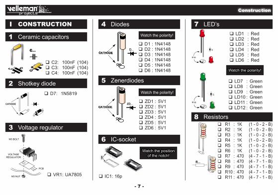
Resistors 8
CONSTRUCTIONI
Ceramic capacitors1
c...
c...
M3 NUT
VOLTAGEREGULATOR
M3 BOLT
PCB
� C2: 100nF (104) � C3: 100nF (104) � C4: 100nF (104)
� D7: 1N5819
Shotkey diode2
Voltage regulator3
Watch the polarity!
Zenerdiodes5
Diodes4
� ZD1 : 5V1 � ZD2 : 5V1 � ZD3 : 5V1 � ZD4 : 5V1 � ZD5 : 5V1 � ZD6 : 5V1
Watch the polarity!
� D1 : 1N4148 � D2 : 1N4148 � D3 : 1N4148 � D4 : 1N4148 � D5 : 1N4148 � D6 : 1N4148
� R1 : 1K (1 - 0 - 2 - B) � R2 : 1K (1 - 0 - 2 - B) � R3 : 1K (1 - 0 - 2 - B) � R4 : 1K (1 - 0 - 2 - B) � R5 : 1K (1 - 0 - 2 - B) � R6 : 1K (1 - 0 - 2 - B) � R7 : 470 (4 - 7 - 1 - B) � R8 : 470 (4 - 7 - 1 - B) � R9 : 470 (4 - 7 - 1 - B) � R10 : 470 (4 - 7 - 1 - B) � R11 : 470 (4 - 7 - 1 - B)
LED’s7
Watch the polarity!
� LD1 : Red � LD2 : Red � LD3 : Red � LD4 : Red � LD5 : Red � LD6 : Red
C (-)
� LD7 : Green � LD8 : Green � LD9 : Green � LD10 : Green � LD11 : Green � LD12 : Green
C (-)
� VR1: UA7805
IC-socket6
� IC1: 16p
Watch the position of the notch!

- 8 -
Construction
Terminal blocks9
� R12 : 470 (4 - 7 - 1 - B) � R13 : 4K7 (4 - 7 - 2 - B) � R14 : 4K7 (4 - 7 - 2 - B) � R15 : 4K7 (4 - 7 - 2 - B) � R16 : 4K7 (4 - 7 - 2 - B) � R17 : 4K7 (4 - 7 - 2 - B) � R18 : 4K7 (4 - 7 - 2 - B)
Relays10 � RY1 � RY2 � RY3 � RY4 � RY5 � RY6
Electrolytic capacitors14
Female headers12
IC15
Watch the polarity!
� C1 : 100µF � C5: 100µF
!
Male header11
DC-jack13
CUT
Analog IN � 3 x 2p
Digital IN � 2 x 3p
INPUTS � D8 : 2p � D9 : 2p � D10 : 2p � D11 : 2p � D12 : 2p � D13 : 2p
V-out � 2 x 2p
� SK16: 3p
� SK15
� 2 x 6p
� 2 x 8p
Do not cut the connector pins!
� IC1: ULN2003
Watch the position of the notch!
- 9 -
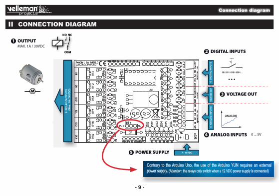
Connection diagram
CONNECTION DIAGRAMII
OUTPUT1MAX. 1A / 30VDC
6 D
IGIT
AL
INP
UT
S6
AN
ALO
G IN
PU
TS
ANALOG
101011101011001...
...
DIGITAL INPUTS2
VOLTAGE OUT3
6 R
EL
AY
OU
TP
UT
S(M
ax.
1A
/ 3
0V
DC
)
0 ... 5VANALOG INPUTS4
VOLT
AG
E O
UT
7 - 15VDCPOWER SUPPLY5
Contrary to the Arduino Uno, the use of the Arduino YUN requires an external power supply. (Attention: the relays only switch when a 12 VDC power supply is connected)

- 10 -
General information
GENERAL INFORMATIONIII
DIGITAL OUTPUT SECTION (FIG.1):The digital outputs correspond to Arduino lines 8, 9, 10, 11, 12 and 13. Each line drives a relay through a transistor.
DIGITAL INPUT SECTION (FIG.2):The digital inputs correspond to Arduino lines 2, 3, 4, 5, 6 and 7, configured as digital input. Protection diodes secure the inputs in case voltages higher than 5 V are applied. Activate the input by bringing it to a low logic level (GND) (inverse logic).1
23456
SK20
Vin
GND5V3V3RST
123456
SK19
A0A1A2A3A4A51
2345678
SK17
ARDUINO UNO
12345678
SK18
01234567
89
10111213
AREF-
-
GND
RELAY TSC112D3HRY1
IN11
IN22
IN33
IN44
IN55
IN66
IN77
OUT1 16
OUT2 15
OUT3 14
OUT4 13
OUT5 12
OUT6 11
OUT7 10
COMD 9GND8
ULN2003A
IC1
RELAY TSC112D3HRY2
RELAY TSC112D3HRY3
RELAY TSC112D3HRY4
RELAY TSC112D3HRY5
RELAY TSC112D3HRY6
123
SK1
123
SK2
123
SK3
123
SK4
123
SK5
123
SK6
LED3RLLD1
1KR1
LED3RLLD2
1KR2
LED3RLLD3
1KR3
LED3RLLD4
1KR4
LED3RLLD5
1KR5
LED3RLLD6
1KR6
89
10111213
D8D9
D10D11D12D13
D8
D9
D10
D12
D11
D13
GND100µ/16-25VC1
100nfC2
GND
LED3RLLD7
LED3RLLD8
LED3RLLD9
LED3RLLD10
LED3RLLD11
LED3RLLD12
470R7
470R8
470R9
470R10
470R11
470R12
1N4148
D1
1N4148
D2
1N4148
D3
1N4148
D4
1N4148
D5
1N4148
D67
6
5
4
3
2DI1
DI2
DI3
DI4
DI5
DI6
JP2SK7
JP2SK8
JP2SK9
JP2SK10
DI1
DI2
DI3
DI4
DI5
DI6
-
JP2SK11
-
4K7
R13
4K7
R14
4K7
R15
4K7
R16
4K7
R17
4K7
R18
AI0
AI1
AI2
AI3
AI4
AI5
A0
A1
A2
A3
A4
A5
5.1V 0.4W
ZD1
5.1V 0.4W
ZD2
5.1V 0.4W
ZD3
5.1V 0.4W
ZD4
5.1V 0.4W
ZD5
5.1V 0.4W
ZD6
GND
JP2SK12
JP2SK13
JP2SK14
AI0
AI1
AI2
AI3
AI4
AI5
SW
-
+
DC JACK
SK15
GND
I O
GN
D
UA7805VR1
GND
123
3PIN HEADERSK16
5V
Vin
VCC
VCC VCC
VCC
VCC
VCC
VCC
VCC
VCC
VCC
VCC
1N5819D7
100nfC3
100nfC4
GND GND
100µ/16-25VC5
GND
Fig.1 Digitial output section
The I/O shield makes it easy to switch loads and handle digital/analogue signals. The digital inputs and outputs feature an LED that show the status of the port.
123456
SK20
Vin
GND5V3V3RST
123456
SK19
A0A1A2A3A4A51
2345678
SK17
ARDUINO UNO
12345678
SK18
01234567
89
10111213
AREF-
-
GND
RELAY TSC112D3HRY1
IN11
IN22
IN33
IN44
IN55
IN66
IN77
OUT1 16
OUT2 15
OUT3 14
OUT4 13
OUT5 12
OUT6 11
OUT7 10
COMD 9GND8
ULN2003A
IC1
RELAY TSC112D3HRY2
RELAY TSC112D3HRY3
RELAY TSC112D3HRY4
RELAY TSC112D3HRY5
RELAY TSC112D3HRY6
123
SK1
123
SK2
123
SK3
123
SK4
123
SK5
123
SK6
LED3RLLD1
1KR1
LED3RLLD2
1KR2
LED3RLLD3
1KR3
LED3RLLD4
1KR4
LED3RLLD5
1KR5
LED3RLLD6
1KR6
89
10111213
D8D9
D10D11D12D13
D8
D9
D10
D12
D11
D13
GND100µ/16-25VC1
100nfC2
GND
LED3RLLD7
LED3RLLD8
LED3RLLD9
LED3RLLD10
LED3RLLD11
LED3RLLD12
470R7
470R8
470R9
470R10
470R11
470R12
1N4148
D1
1N4148
D2
1N4148
D3
1N4148
D4
1N4148
D5
1N4148
D67
6
5
4
3
2DI1
DI2
DI3
DI4
DI5
DI6
JP2SK7
JP2SK8
JP2SK9
JP2SK10
DI1
DI2
DI3
DI4
DI5
DI6
-
JP2SK11
-
4K7
R13
4K7
R14
4K7
R15
4K7
R16
4K7
R17
4K7
R18
AI0
AI1
AI2
AI3
AI4
AI5
A0
A1
A2
A3
A4
A5
5.1V 0.4W
ZD1
5.1V 0.4W
ZD2
5.1V 0.4W
ZD3
5.1V 0.4W
ZD4
5.1V 0.4W
ZD5
5.1V 0.4W
ZD6
GND
JP2SK12
JP2SK13
JP2SK14
AI0
AI1
AI2
AI3
AI4
AI5
SW
-
+
DC JACK
SK15
GND
I O
GN
D
UA7805VR1
GND
123
3PIN HEADERSK16
5V
Vin
VCC
VCC VCC
VCC
VCC
VCC
VCC
VCC
VCC
VCC
VCC
1N5819D7
100nfC3
100nfC4
GND GND
100µ/16-25VC5
GND
Fig.2 Digitial input section

- 11 -
General information
ANALOGUE OUTPUTS (PWM):
Lines 3, 5 and 6 can be configured as analogue output (PWM, +5 V). With a value between 0 and 255, the duty cycle can vary between 0 and 100 %. Attention: The LED will have an inverse logic in this mode: 0 % duty cycle = LED on, 100 % duty cycle = LED off. All digital inputs have a common ground (GND).
ANALOGUE INPUT SECTION (FIG.3):
Each analogue input (A0..A5) features a series resistor and a protection diode.
The shield requires an external power supply (9-12 VDC).Place jumper JP5V between the central pin and the PWR pin. In this way, the shield as the Arduino Yun are powered by their own power supply.You can also use the shield with a classic Arduino board, which can be equipped with a power supply. Place the jumper between the central pin and 5 V pin. The Yun does not allow this because of the higher current absorption.
Fig.3 Analogue output section
123456
SK20
Vin
GND5V3V3RST
123456
SK19
A0A1A2A3A4A51
2345678
SK17
ARDUINO UNO
12345678
SK18
01234567
89
10111213
AREF-
-
GND
RELAY TSC112D3HRY1
IN11
IN22
IN33
IN44
IN55
IN66
IN77
OUT1 16
OUT2 15
OUT3 14
OUT4 13
OUT5 12
OUT6 11
OUT7 10
COMD 9GND8
ULN2003A
IC1
RELAY TSC112D3HRY2
RELAY TSC112D3HRY3
RELAY TSC112D3HRY4
RELAY TSC112D3HRY5
RELAY TSC112D3HRY6
123
SK1
123
SK2
123
SK3
123
SK4
123
SK5
123
SK6
LED3RLLD1
1KR1
LED3RLLD2
1KR2
LED3RLLD3
1KR3
LED3RLLD4
1KR4
LED3RLLD5
1KR5
LED3RLLD6
1KR6
89
10111213
D8D9
D10D11D12D13
D8
D9
D10
D12
D11
D13
GND100µ/16-25VC1
100nfC2
GND
LED3RLLD7
LED3RLLD8
LED3RLLD9
LED3RLLD10
LED3RLLD11
LED3RLLD12
470R7
470R8
470R9
470R10
470R11
470R12
1N4148
D1
1N4148
D2
1N4148
D3
1N4148
D4
1N4148
D5
1N4148
D67
6
5
4
3
2DI1
DI2
DI3
DI4
DI5
DI6
JP2SK7
JP2SK8
JP2SK9
JP2SK10
DI1
DI2
DI3
DI4
DI5
DI6
-
JP2SK11
-
4K7
R13
4K7
R14
4K7
R15
4K7
R16
4K7
R17
4K7
R18
AI0
AI1
AI2
AI3
AI4
AI5
A0
A1
A2
A3
A4
A5
5.1V 0.4W
ZD1
5.1V 0.4W
ZD2
5.1V 0.4W
ZD3
5.1V 0.4W
ZD4
5.1V 0.4W
ZD5
5.1V 0.4W
ZD6
GND
JP2SK12
JP2SK13
JP2SK14
AI0
AI1
AI2
AI3
AI4
AI5
SW
-
+
DC JACK
SK15
GND
I O
GN
D
UA7805VR1
GND
123
3PIN HEADERSK16
5V
Vin
VCC
VCC VCC
VCC
VCC
VCC
VCC
VCC
VCC
VCC
VCC
1N5819D7
100nfC3
100nfC4
GND GND
100µ/16-25VC5
GND

- 12 -
123456
SK20
Vin
GND5V3V3RST
123456
SK19
A0A1A2A3A4A51
2345678
SK17
ARDUINO UNO
12345678
SK18
01234567
89
10111213
AREF-
-
GND
RELAY TSC112D3HRY1
IN11
IN22
IN33
IN44
IN55
IN66
IN77
OUT1 16
OUT2 15
OUT3 14
OUT4 13
OUT5 12
OUT6 11
OUT7 10
COMD 9GND8
ULN2003A
IC1
RELAY TSC112D3HRY2
RELAY TSC112D3HRY3
RELAY TSC112D3HRY4
RELAY TSC112D3HRY5
RELAY TSC112D3HRY6
123
SK1
123
SK2
123
SK3
123
SK4
123
SK5
123
SK6
LED3RLLD1
1KR1
LED3RLLD2
1KR2
LED3RLLD3
1KR3
LED3RLLD4
1KR4
LED3RLLD5
1KR5
LED3RLLD6
1KR6
89
10111213
D8D9
D10D11D12D13
D8
D9
D10
D12
D11
D13
GND100µ/16-25VC1
100nfC2
GND
LED3RLLD7
LED3RLLD8
LED3RLLD9
LED3RLLD10
LED3RLLD11
LED3RLLD12
470R7
470R8
470R9
470R10
470R11
470R12
1N4148
D1
1N4148
D2
1N4148
D3
1N4148
D4
1N4148
D5
1N4148
D67
6
5
4
3
2DI1
DI2
DI3
DI4
DI5
DI6
JP2SK7
JP2SK8
JP2SK9
JP2SK10
DI1
DI2
DI3
DI4
DI5
DI6
-
JP2SK11
-
4K7
R13
4K7
R14
4K7
R15
4K7
R16
4K7
R17
4K7
R18
AI0
AI1
AI2
AI3
AI4
AI5
A0
A1
A2
A3
A4
A5
5.1V 0.4W
ZD1
5.1V 0.4W
ZD2
5.1V 0.4W
ZD3
5.1V 0.4W
ZD4
5.1V 0.4W
ZD5
5.1V 0.4W
ZD6
GND
JP2SK12
JP2SK13
JP2SK14
AI0
AI1
AI2
AI3
AI4
AI5
SW
-
+
DC JACK
SK15
GND
I O
GN
D
UA7805VR1
GND
123
3PIN HEADERSK16
5V
Vin
VCC
VCC VCC
VCC
VCC
VCC
VCC
VCC
VCC
VCC
VCC
1N5819D7
100nfC3
100nfC4
GND GND
100µ/16-25VC5
GND
Connection diagram

- 13 -
PCB

Supply voltage (V) - led voltage (V)
required current (A)= series resistance (ohms)
required current (A)= series resistance (ohms)
Required resistor power handling= voltage over resistor x current passed trough resistor
9V - 1.7V
0.005A= 1460 ohm
9V - (3 x1.7V)
0.005A= 780 ohm
(9V - 1.7V) x 0.005A = 0.036W
closest value : use a 1k5 resistor
use an 820 ohm resistor
a standard 1/4W resistor will do the job
Supply voltage (V) - (number of leds x led voltage (V))
How to Calculate the series resistor:Example: operate a red led (1.7V) on a 9Vdc source. Required led current for full brightness: 5mA (this can be found in the datasheet of the led)
LEDs in series:
Example: 3 x red led (1.7V) on 9V battery Required led current for full brightness: 5mA (this can be found in the datasheet of the led)
Leds feature a specific voltage drop, depending on type and colour. Check the datasheet for exact voltage drop and rated current !
Never connect leds in parallel
Leds and how to use them
An open collector output can be compared to a switch which switches to ground when operated
Example: How to switch an LED by means of an open collector output
open collector outputs


The new Velleman Projects catalogue is now available. Download your copy here:
www.vellemanprojects.eu
Modifications and typographical errors reserved - © Velleman nv. HKA08’IP Velleman NV, Legen Heirweg 33 - 9890 Gavere.