k-maps, timing sequential circuits: latches & flip-flops lecture 4 digital design and computer...
TRANSCRIPT

K-Maps, TimingK-Maps, TimingSequential Circuits: Latches & Flip-FlopsSequential Circuits: Latches & Flip-Flops
Lecture 4Digital Design and Computer Architecture
Harris & HarrisMorgan Kaufmann / Elsevier, 2007

2.7 3-input K-map2.7 3-input K-map
C 00 01
0
1
Y
11 10AB
ABC
ABC
ABC
ABC
ABC
ABC
ABC
ABC
1 0
B C Y0 0 00 1 01 01 1 1
Truth Table
C 00 01
0
1
Y
11 10ABA
0000
0 0 00 1 11 0 01 1 0
1111
0
1
1
0
0
0
1
K-Map

3-input K-map3-input K-map
C 00 01
0
1
Y
11 10AB
ABC
ABC
ABC
ABC
ABC
ABC
ABC
ABC
1 0
B C Y0 0 00 1 01 01 1 1
Truth Table
C 00 01
0
1
Y
11 10ABA
0000
0 0 00 1 01 0 01 1 1
1111
0
1
1
1
0
0
0
K-Map

K-map DefinitionsK-map Definitions
• Complement: variable with a bar over it
• Literal: variable or its complement
• Implicant: product of literals
• Prime implicant: implicant corresponding to the larges circle in the K-map

K-map RulesK-map Rules
• Each circle must span a power of 2 (i.e. 1, 2, 4) squares in each direction
• Each circle must be as large as possible• A circle may wrap around the edges of the K-
map• A one in a K-map may be circled multiple
times• A “don't care” (X) is circled only if it helps
minimize the equation

4-input K-map4-input K-map
01 11
1
0
0
1
0
0
1
101
1
1
1
1
0
0
0
1
11
10
AB00
00
10CD
Y
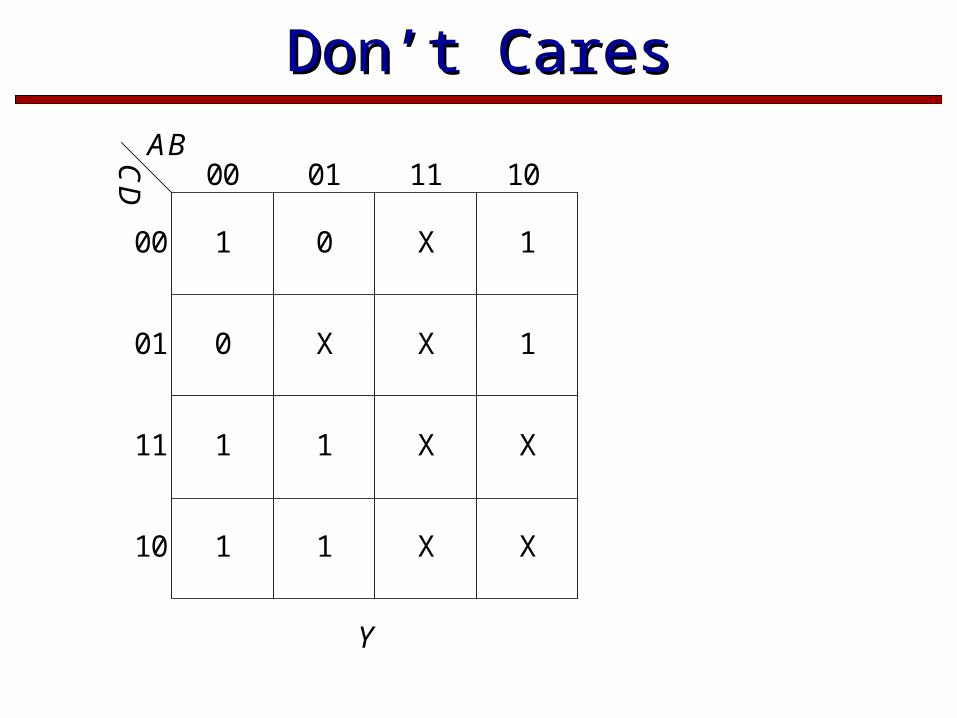
Don’t CaresDon’t Cares
01 11
1
0
0
X
X
X
1
101
1
1
1
1
X
X
X
X
11
10
CD
AB00
00
10
Y

Contention: XContention: X
• Not just 1’s and 0’s• Contention: X
A = 1
Y = X
B = 0

Floating: ZFloating: Z
Tri-state Buffer
E A Y0 0 Z0 1 Z1 0 01 1 1
A
E
Y

2.8 Building Blocks2.8 Building Blocks
• Multiplexer vs. Demultiplexer• Decoder vs. Encoder• Priority Encoder• Adder

MultiplexersMultiplexers
Y0 00 11 01 1
0101
0000
0 00 11 01 1
1111
0011
0
1
S
D0Y
D1
D1 D0S
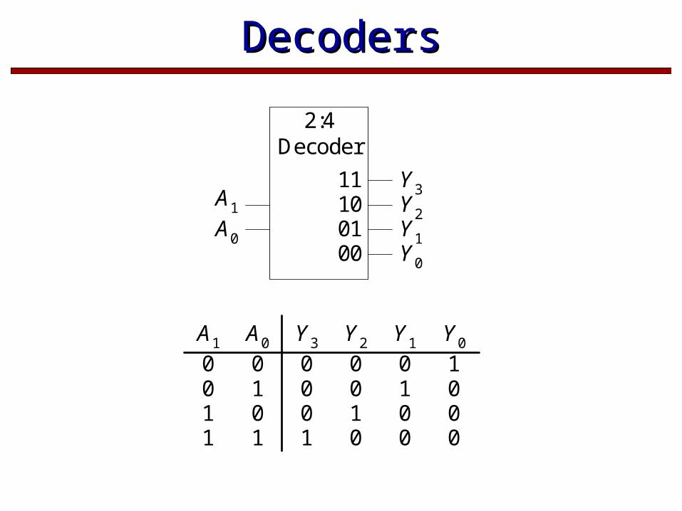
DecodersDecoders
2:4Decoder
A1
A0
Y3Y2Y1Y000
011011
0 00 11 01 1
0001
Y3 Y2 Y1 Y0A0A1
0010
0100
1000

2.9 Timing2.9 Timing
• See chap08.ppt of last year.

2.9.1 Propagation & Contamination Delay2.9.1 Propagation & Contamination Delay
• Propagation Delay: tpd = max delay from input to output
• Contamination Delay: tcd = min delay from input to output
A
Y
Time
A Y
tpd
tcd

Critical (Long) and Short PathCritical (Long) and Short Path
AB
C
D Y

2.9.2 Glitches2.9.2 Glitches
• Glitch: when a single input change causes multiple output changes
• Glitches don’t cause problems because of synchronous design conventions (which we’ll talk about in a bit)
• But it’s important to recognize a glitch when you see one in timing diagrams

Glitches: ExampleGlitches: Example
AB
C
Y
00 01
1
Y
11 10AB
1
1
0
1
0
1
0
0
C
0
Y = AB + BC

Glitches: ExampleGlitches: Example
00 01
1
Y
11 10AB
1
1
0
1
0
1
0
0
C
0
Y = AB + BC + ACAC
B = 1 0Y = 1
A = 0
C = 1

Ch.3 Sequential CircuitsCh.3 Sequential Circuits
• Circuits that:– give sequence to events– have memory (short-term)– use feedback from output to input

3.2 State Elements3.2 State Elements
• State: information that determines future behavior of circuit
• State elements store state– Cross coupled inverter pair– SR Latch– D Latch– D Flip-flop

Cross Coupled inverter pairCross Coupled inverter pair
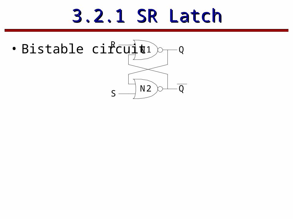
3.2.1 SR Latch3.2.1 SR Latch
R
S
Q
Q
N1
N2
• Bistable circuit
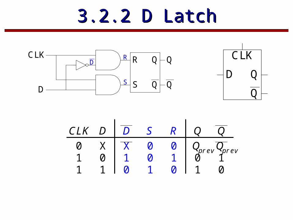
3.2.2 D Latch3.2.2 D Latch
S
R Q
Q
Q
QD
CLKD
R
S
CLK
D Q
Q
S R Q
0 0 Qprev0 1 01 0 1
Q
10
CLK D
0 X1 01 1
D
X10
Qprev

3.2.3 D Flip-Flop3.2.3 D Flip-Flop
CLK
D Q
Q
CLK
D Q
Q
Q
Q
DN1
CLK
L1 L2
master slave
D Q
Q
How many transistors required for a D-FF ?

3.2.4 Registers3.2.4 Registers
CLK
D Q
D Q
D Q
D Q
D0
D1
D2
D3
Q0
Q1
Q2
Q3
D3:0
4 4
CLK
Q3:0

3.2.5x3.2.5x Enabled & Resettable Enabled & Resettable FFFF

Eg.3.2– D-FF vs. D LatchEg.3.2– D-FF vs. D Latch
CLK
D Q
Q
D Q
Q
CLK
D
Q (latch)
Q (flop)

D Flip-Flop Input Timing ConstraintsD Flip-Flop Input Timing Constraints
CLK
tsetup
D
thold
• Setup time: tsetup = time before the clock edge that data must be stable (i.e. not changing)
• Setup time: thold = time after the clock edge that data must be stable
• Aperture time: To = time around clock edge that data must be stable
D Q
Q

D Flip-Flop Output TimingD Flip-Flop Output Timing
• Propagation Delay: tpcq = time after clock edge that Q is guaranteed to be stable (i.e. stop changing)
• Contamination Delay: tccq = time after clock edge that Q might be unstable (i.e. start changing)
D Q
Q
CLK
tccq
tpcq
tsetup
Q
D
thold

3.3 Synchronous Logic Design3.3 Synchronous Logic Design
• 3.3.1 Some Problematic Circuits

3.3.2 Sync. Seq. circuits3.3.2 Sync. Seq. circuits

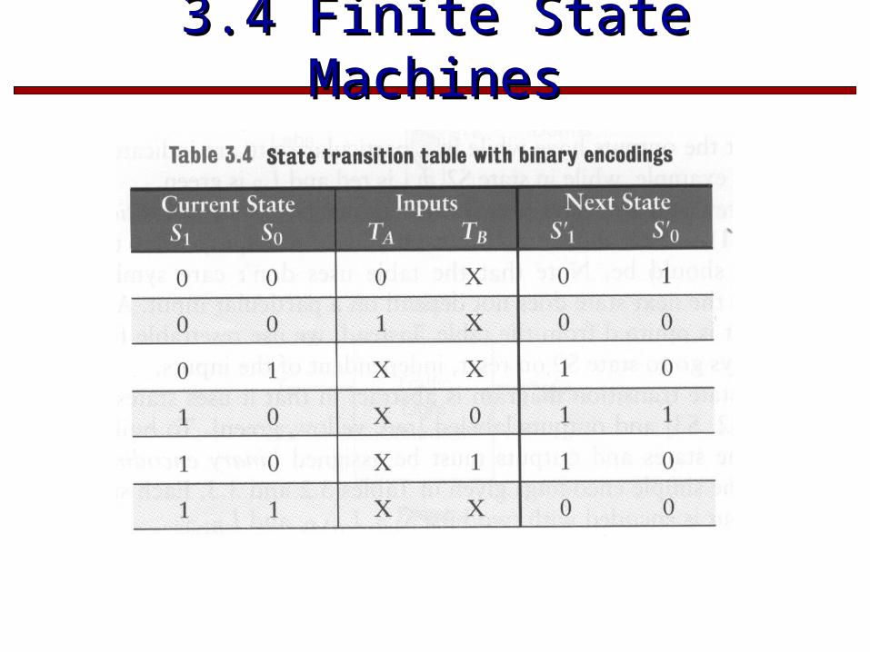
3.4 Finite State Machines3.4 Finite State Machines
• Moore & Mealy Machine

3.4 Finite State Machines3.4 Finite State Machines

3.4 Finite State Machines3.4 Finite State Machines

3.4 Finite State Machines3.4 Finite State Machines
3.4 Finite State Machines3.4 Finite State Machines

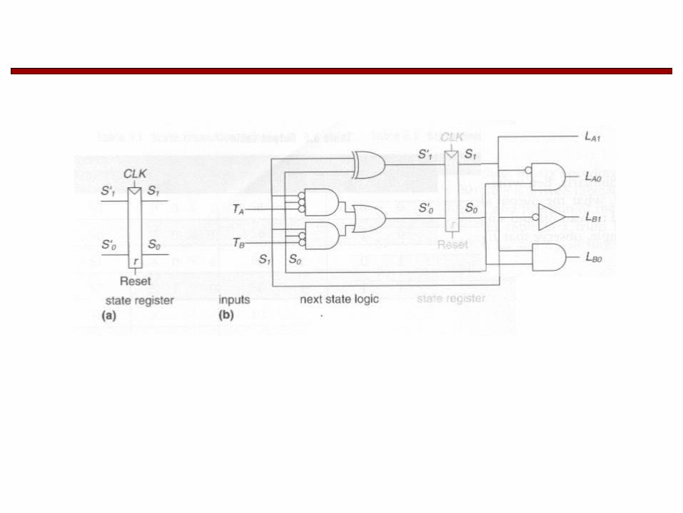


3.4.2 State Encoding3.4.2 State Encoding
• Divide by N counter


Next TimeNext Time
• Finite State Machines