journal of microelectromechanical …web.eecs.umich.edu/~minar/pdf/gan_review.pdf ·...
TRANSCRIPT

This article has been accepted for inclusion in a future issue of this journal. Content is final as presented, with the exception of pagination.
JOURNAL OF MICROELECTROMECHANICAL SYSTEMS 1
Gallium Nitride as an Electromechanical MaterialMina Rais-Zadeh, Senior Member, IEEE, Vikrant Jayant Gokhale, Student Member, IEEE,
Azadeh Ansari, Student Member, IEEE, Marc Faucher, Didier Théron, Member, IEEE,Yvon Cordier, and Lionel Buchaillot, Member, IEEE
Abstract— Gallium nitride (GaN) is a wide bandgap semicon-ductor material and is the most popular material after siliconin the semiconductor industry. The prime movers behind thistrend are LEDs, microwave, and more recently, power electronics.New areas of research also include spintronics and nanoribbontransistors, which leverage some of the unique properties of GaN.GaN has electron mobility comparable with silicon, but witha bandgap that is three times larger, making it an excellentcandidate for high-power applications and high-temperatureoperation. The ability to form thin-AlGaN/GaN heterostruc-tures, which exhibit the 2-D electron gas phenomenon leads tohigh-electron mobility transistors, which exhibit high Johnson’sfigure of merit. Another interesting direction for GaN research,which is largely unexplored, is GaN-based micromechani-cal devices or GaN microelectromechanical systems (MEMS).To fully unlock the potential of GaN and realize new advancedall-GaN integrated circuits, it is essential to cointegrate pas-sive devices (such as resonators and filters), sensors (such astemperature and gas sensors), and other more than Moorefunctional devices with GaN active electronics. Therefore, thereis a growing interest in the use of GaN as a mechanical material.This paper reviews the electromechanical, thermal, acoustic,and piezoelectric properties of GaN, and describes the workingprinciple of some of the reported high-performance GaN-basedmicroelectromechanical components. It also provides an outlookfor possible research directions in GaN MEMS. [2014-0147]
Index Terms— III-V, HEMT, microelectromechanicalsystems, micromachining, piezoelectric materials, resonators,wide bandgap.
I. INTRODUCTION
OVER THE recent few years, GaN has become oneof the most popular semiconductor materials [1]–[3].
As with any other growing industry, fundamental break-throughs in material science and device technologies have beenaided by rapid improvements in the fabrication and processing
Manuscript received May 8, 2014; revised July 11, 2014; acceptedAugust 22, 2014. This work was supported in part by the U.S. NationalScience Foundation under Award 1002036 and Award 1055308; in part bythe U.S. Army Research Laboratory, Adelphi, MD, USA, through the MicroAutonomous Systems and Technology Collaborative Technology Allianceunder Contract W911NF; and in part by the French National Research Agencyunder Contract ANR-08-NANO-023. Subject Editor G. Piazza.
M. Rais-Zadeh, V. J. Gokhale, and A. Ansari are with the Univer-sity of Michigan, Ann Arbor, MI 48109 USA (e-mail: [email protected];[email protected]; [email protected]).
M. Faucher, D. Theron, and L. Buchaillot are with the Institutd’Electronique de Microélectronique et de Nanotechnologie, Villeneuved’Ascq 59652, France (e-mail: [email protected];[email protected]; [email protected]).
Y. Cordier is with the Centre de Recherche sur l’Hétéro-Epitaxie et sesApplications, Valbonne 06560, France (e-mail: [email protected]).
Color versions of one or more of the figures in this paper are availableonline at http://ieeexplore.ieee.org.
Digital Object Identifier 10.1109/JMEMS.2014.2352617
TABLE I
PROPERTIES OF A SELECTION OF ELECTROMECHANICAL MATERIALS
techniques [1], [2] with consistent improvements in wafersize, material quality, diversification of epitaxial substratematerial, and ease of market access. While the current costof GaN substrates is high, based on the economics of scale,high-volume production of GaN wafers is expected to reducethe wafer cost to the same level as GaAs substrates [1].In addition, epitaxial growth of high-quality GaN on low-costsubstrates, such as silicon (Si), is becoming more mature. Thiswould make GaN one of the cheapest semiconductors, secondonly to Si.
The growth of GaN semiconductor industry has beenfueled primarily by those segments devoted to optoelectron-ics, driving material improvement, followed by high-powerelectronics and radio-frequency (RF) electronics, which takeadvantage of the wide bandgap and high breakdown capabil-ities of this material. While a significant amount of scientificresearch has been devoted to the applications mentioned above,little attention has been given to the use of GaN for nanoand microelectromechanical systems (N/MEMS). Unlike Si,GaN is a piezoelectric semiconductor and one can envisionusing the piezoelectric properties of GaN alone to manufacturemultitude of devices for diverse applications. Besides beinga piezoelectric, GaN offers several other advantages as anelectromechanical material.
A selection of some of the pertinent material fig-ures of merit (FOM) of GaN is compared with a selec-tion of other commonly used electromechanical materialsin Table I. It can be seen that GaN is one of the most
1057-7157 © 2014 IEEE. Translations and content mining are permitted for academic research only. Personal use is also permitted,but republication/redistribution requires IEEE permission. See http://www.ieee.org/publications_standards/publications/rights/index.html for more information

This article has been accepted for inclusion in a future issue of this journal. Content is final as presented, with the exception of pagination.
2 JOURNAL OF MICROELECTROMECHANICAL SYSTEMS
versatile materials available for use in electromechanicalsystems.
A large amount of research has gone into characterizingthe growth, processing, electrical and optical properties ofGaN. However, broader understanding of the material isnecessary in order to explore more applications that canbe enabled by affordable high-quality GaN. The purposeof this work is to provide the most recent data on theelectromechanical properties of GaN grown epitaxially on Sisubstrates, review its current use in MEMS applications witha special focus on RF MEMS and GaN resonant microde-vices, and provide possible directions for GaN NEMS/MEMSresearch.
II. ELECTROMECHANICAL PROPERTIES OF GaN
A. Crystallinity of GaN on Si
A wide range of techniques have been used to growthin-film GaN on a substrate, such as metal organic vaporphase epitaxy (MOVPE) and molecular beam epitaxy (MBE).A variety of substrates such as Si, silicon carbide (SiC), andsapphire have been used for these studies [2]. Most of thefilms grown have wurtzite crystalline structure and have n-typeconductivity [2], although Zinc blende GaN growth has alsobeen reported. Intentional p-type doping of GaN is alsopossible [19]. In this paper, we focus on properties of GaNgrown on Si. GaN-on-Si substrates are attractive candidatesfor GaN MEMS and GaN movable mechanical compo-nents with Si selectively removed underneath GaN structures.GaN-on-Si is also an attractive substrate for implementingGaN devices integrated with Si-based large scale integratedcircuits, although the highest quality GaN films have beenobtained on Si (111) or Si (110) and not on Si (100).
GaN in its wurtzite form has a crystal structure with latticeparameters of a = 3.189Å and c = 5.185Å. A figureof merit that is commonly used to characterize the intrin-sic crystalline quality of an epitaxially grown thin film isthe Full Width at Half Maximum (FWHM) acquired usingX-Ray Diffraction (XRD) analysis. A narrow FWHM denoteshigh long-range crystalline order and good internal alignmentof the crystal (Fig. 1). However, special care has to be takenconcerning the symmetric (000l) XRD reflection line width,which in the case of thick films is mostly sensitive to theso-called (low-density) screw-type threading dislocations.XRD reflection lines measured for oblique crystal planes, suchas (10-12) or (30-32), are much more relevant because they aresensitive to almost all the threading defects. However, theseare sometimes not reported.
To achieve good FWHM values for GaN-on-Si, it is oftennecessary to grow a thin layer of AlN or a graded AlN/AlGaNbuffer layer to avoid chemical reactions between gallium andsilicon and to accommodate the lattice mismatch betweenthe substrate and the epitaxial GaN. Table II lists reported(0002) XRD FWHM values of GaN grown on the mostcommonly used substrates. It should be noted that the recentresults for GaN-on-Si [20] demonstrated by Pinos et al.in 2014 exhibit FWHM values comparable to high-qualityGaN films grown on sapphire [21], [22]. Recent results
Fig. 1. A representative result showing XRD spectroscopy on a GaN thin filmgrown on a Si (111) substrate using metal-organic chemical vapor deposition(MOCVD). Inset: Rocking curve of the (0002) GaN plane exhibits a veryclear peak and a FWHM of 1296 arcsec. Films were measured using a RigakuUltima IV XRD system.
TABLE II
CRYSTALLINE QUALITY OF THIN FILM GaN
measured at the University of Michigan (UM) are acquiredusing a Rigaku Ultima IV X-ray diffractometer, on bare,unprocessed GaN films.
B. In-Situ Stress Measurements During Growth
In-situ wafer curvature measurements are helpful to under-stand the evolution of the stress profile within the grownmaterials. Here, an MBE reactor is used to grow GaN-on-Si onAlN nucleation layers with an initial compressive strain relatedto the in-plane lattice parameter mismatch of 2.5% betweenthe two materials. A large part of the mismatch is rapidlyrelaxed via the introduction or the bending of dislocations.However, depending on the epitaxial layer sequence grownbefore the final GaN layer, the remaining part of the stresscan vary significantly within the layer. In these structures AlNis grown at 920 °C and GaN at 800 °C. Fig. 2 illustrates thevariation in the substrate curvature while growing a 1 μm thickGaN film on a 0.2 μm AlN nucleation layer compared to a1.7 μm GaN film on AlN/GaN/AlN (80 nm/ 0.25 μm/42 nm)stress mitigating stack.
In the absence of inter-layers, the compressive stress in GaNgrown on AlN is rapidly relaxed and the negative curvature

This article has been accepted for inclusion in a future issue of this journal. Content is final as presented, with the exception of pagination.
RAIS-ZADEH et al.: GaN AS AN ELECTROMECHANICAL MATERIAL 3
Fig. 2. Substrate curvature for GaN films grown by MBE on AlN (gray) andon AlN/GaN/AlN stress mitigating (black) layers. The addition of the stressmitigating layers enables the growth of thick GaN structures on a Si substrate.
(convex bowing) saturates at a rather low level before itreaches positive values (concave bowing) upon cooling downat the end of the growth (here from 800 °C to room temper-ature (RT)). Such a behavior upon cooling is caused by themismatch between the thermal expansion coefficient (TEC) ofGaN and Si. On the contrary, GaN grown on stress mitigatinglayers induces a noticeable convex substrate bowing even aftergrowth of more than 1.7 μm thick GaN [25]. Moreover,the non-linear evolution of the curvature accounts for thepresence of a stress gradient varying from compressive in thevicinity of the interface with AlN to almost relaxed towardsthe surface. Such a structure is able to maintain a convexsubstrate bowing upon cooling down in-spite of its largerthickness. This way, thick structures can be grown crack-freewith a better crystal quality, but with a risk of buckling whilereleasing membranes or clamped beams. One important pointis that the stress responsible for the substrate bowing at thegrowth temperature is still present at room temperature, butshifted by the additional stress (∼1 GPa) due to the TECmismatch between GaN and Si. Then, as compared to growthtemperature, the stress profile shall be almost unchanged atroom temperature after the release from the substrate. Thus,the in-situ curvature measurement is helpful to understandthe behavior of released beams or membranes. As shown inFig. 3, low-temperature photoluminescence [25] performed onGaN layers of various thicknesses with and without stressmitigating layers confirms the presence of stress gradients.In simple structures, a tensile stress develops from almost zeroup to 1 GPa, confirming the rapid stress relaxation in GaN atthe growth temperature. In the presence of stress mitigatingstacks, the stress ranges from about −2 GPa (compressive)in the bottom part of the GaN film up to less than +0.3GPa (tensile) in the upper part. When releasing the structuresfrom the substrate, the data plotted in Fig. 3 shall be shiftedby −1 GPa. It is worth to mention that the efficiency of theinter-layers for stress mitigation depends on the crystal qualityof the nucleation process, which itself affects the requiredthickness of each stress-mitigation layer: for instance, progressin Si surface preparation led us to reduce the AlN inter-layer
Fig. 3. In-plane stress acquired using low-temperature photoluminescencemeasurements for GaN layers with various thicknesses, grown on multiplesamples. A marked difference is seen due to the presence (diamonds) orabsence (triangles) of stress mitigating layers. Each color represents data forone sample. The lines are guides for the eyes.
thickness from 0.25 μm in [25] down to 75 nm in somecases. The 0.25 μm GaN can also be replaced by a 0.25 μmAl0.15Ga0.85N inter-layer for a better electrical isolation [26].Even when other thicknesses are used, the principle ofinter-layers has shown its efficiency for growing thick GaNfilms on Si by MOVPE (Table III) [27].
At present, good crystal quality samples have been devel-oped on structures with buffer layers not optimized for MEMSapplications while efforts have to be made in the future toenhance the crystal quality of simple thin structures (withoutstress mitigating stacks) that are more promising from amechanical point of view. As the risk of layer cracking beforethe release from the substrate is higher in the absence of stressmitigating stacks, it is crucial to grow optimized films carefullyto get GaN films with reasonable total stress before and uponthe release from the substrate.
C. Mechanical Properties of GaN
The mass density of GaN has been quoted in the literatureas 6095 kg/m3 [28], [29] or 6150 kg/m3 [2]. Due to itshexagonal nature, the elastic properties of wurtzite GaN aresymmetric along the in-plane vectors. The elastic moduli ofw-GaN have been calculated by Wright using ab-initio densityfield calculations [30] and verified using Brillouin scatteringby Yamaguchi et al. [31] and Polian et al. [28]. The fullstiffness matrix for GaN is given by Cij , as shown at thebottom of the next page.
The elastic compliance and constants for the binary com-pounds as well as the rule to obtain the values for alloysare summarized by Ambacher et al. [2]. Knoop hardness ofGaN was reported to be 14.21 GPa [2] and agrees well withexperimental data obtained for GaN-on-Si samples in thiswork (Table III). The majority of these films are grown withinter-layers to avoid cracks.
The microhardness of single crystal GaN thin films isreported to be 10.2–19 GPa [2], [37]. In order to verifythe previously reported values, nanoindentation experimentswere carried out recently at both University of Michigan

This article has been accepted for inclusion in a future issue of this journal. Content is final as presented, with the exception of pagination.
4 JOURNAL OF MICROELECTROMECHANICAL SYSTEMS
TABLE III
MECHANICAL PROPERTIES OF GaN (IL STANDS FOR INTER-LAYERS)
and at IEMN. These previously unpublished results largelysupport prior data. Here, nanoindentation experimentsleading to the mechanical properties of GaN films have beenobtained by means of a MTS NanoXP® nanoindenter (AgilentTechnologies Inc., Oak Ridge, TN, USA) at IEMN using aBerkovich tip. The equipment is installed in a clean-roomwhere temperature and humidity are monitored and main-tained constant. A NanoInstruments Nanoindenter II with aBerkovich tip was used at UM. Both sets of nanoindenta-tion measurements were performed on bare samples of thespecified GaN film using the continuous stiffness measure-ment (CSM) method, where a small oscillation is superim-posed to the primary loading signal [38]. Nanoindentationtests carried out in the course of this work indicate thatthe hardness for different types of substrates and fabricationmethods consistently lies in the range of 20-26 GPa (Fig. 4).GaN Young’s moduli reported in Table III are higher whenthe material is directly grown on bulk c-Sapphire or when thelayers are thick enough on (111) Si substrate. It is significantlylower when the thickness of GaN grown on Si is inferior to3 μm (Fig. 5), indicating probable influence of the crystalquality on the Young’s modulus.
D. Piezoelectric Properties of GaN
The use of GaN as an electromechanical material ispredicated on its piezoelectric properties. Piezoelectric actu-ation can be used for both static as well as dynamic actu-ation/sensing, with frequencies as high as tens of GHz.As a piezoelectrically actuated vibrating or resonant system,
Fig. 4. Hardness for eight different GaN films used to in this work. Thedata are measured using a Berkovich tip nanoindenter. The values representan average of at least eight indents on each sample.
Fig. 5. Young’s modulus for eight different GaN films used in this work. Thedata are measured using a Berkovich tip nanoindenter. The values representan average of at least eight indents on each sample.
GaN has the advantage of high coupling efficiency comparedto similar devices using capacitive, thermal, or magneticactuation. A large number of devices discussed in this revieware based on the piezoelectric transduction principle. Thepiezoelectric coefficients of wurtzite GaN have been calculatedby Bykhovski et al. [39] to be
ei j =⎛⎝ 0 0 0 0 −0.3 0
0 0 0 −0.3 0 0−0.33 −0.33 +0.65 0 0 0
⎞⎠ Cm−2
Cij =
⎛⎜⎜⎜⎜⎜⎜⎝
390 ± 25 145 ± 20 106 ± 20 0 0 0145 ± 20 390 ± 15 106 ± 20 0 0 0106 ± 20 106 ± 20 398 ± 20 0 0 0
0 0 0 105 ± 10 0 00 0 0 0 105 ± 10 00 0 0 0 0 122.5 ± 20
⎞⎟⎟⎟⎟⎟⎟⎠
G Pa

This article has been accepted for inclusion in a future issue of this journal. Content is final as presented, with the exception of pagination.
RAIS-ZADEH et al.: GaN AS AN ELECTROMECHANICAL MATERIAL 5
These and very similar values [40] are popularly used bymany subsequent researchers. Bernardini et al. [41] andShur et al. [42] calculate different values of 0.73 Cm−2 and−0.49 Cm−2 for e33 and e31, respectively. Cimalla et al. [2]reported similar vales in a review of a number of theoreticaland measured results (using interferometry and atomic forcemicroscopy) for the piezoelectric constants of GaN and con-cluded that the film structure and quality highly influences theexact numbers.
E. Thermal Properties of GaN
As a material intended for high-power or high-temperatureelectronics and capable of operating in harsh environments,it is useful to know the thermal properties of GaN. Thethermal conductivity of GaN is highly dependent on the filmquality, the concentration and type of impurities and defectspresent, and the temperature. Experimental results for thermalconductivity of GaN indicate that the room temperature valuesfor thermal conductivity are within the range of 100 W/m-Kto 250 W/m-K [43]–[45]. The thermal conductivity showsan inverse relation with the doping and impurity con-centration [46], [47]. The decrease was attributed mostlyto the increased phonon relaxation on dopants. Measuredvalues agree well with theoretical estimates [48]. TheDebye temperature for wurtzite GaN has been calculatedas 618 K to 641 K [31], [49]. The specific heat capac-ity of GaN is in the range of 300 J/kg-K to 500 J/kg-Kat room temperature [6], [50]. GaN coefficient of thermalexpansion (β) is on the order of 3 × 10⁻⁶ K−1 along thec-axis [6], [50], and in the range of 3.8 × 10⁻⁶ K−1 to5.6 × 10−6 K−1 in-plane [6], [50]. GaN is also known to bea very strong pyroelectric material [42], [51] with an expectedpyroelectric voltage coefficient (Pv = 7 × 10⁵ V/m-K) greaterthan the proven high-temperature pyroelectric material lithiumtantalite (Pv = 5× 10⁵ V/m-K) [42]. Experimental results havedemonstrated values of Pv up to 1 × 10⁴ V/m-K [51] andfurther investigation is necessary to utilize the full potentialof GaN-based pyroelectric devices.
F. Electrical Properties of GaN
Extensive research has been recently conducted on com-pound semiconductor materials, motivated by their superiormaterial properties as compared to Si. GaN, as the secondmost popular semiconductor, with a bandgap energy ofEg = 3.4 eV at room temperature, offers high breakdownelectric field, high thermal conductivity, high peak velocity,and high saturation velocity. Further contributing to the out-standing material properties of GaN, is the ability to achievetwo-dimensional electron gases (2DEG) with sheet carrierconcentrations of more than 1013 cm−2 and high elec-tron mobility of more than 2000 cm2/V-s at AlGaN/GaNhetero-interface without intentional doping. The excellentelectrical properties of AlGaN/GaN high electron mobilitytransistors (HEMTs) make it a perfect candidate for high-frequency, high-temperature, and high-power operations. Par-ticularly, AlGaN/GaN hetero-structures, show clear advantagesover other material systems such as GaAs, SiC, and Si
TABLE IV
ELECTRICAL PROPERTIES OF GaN
Fig. 6. Calculated slowness curves for GaN for in-plane and out-of-plane acoustic wave propagation. The green shaded regions indicate theslowness values extracted from the frequency of resonators fabricated at UMand [16], [17], [57]–[61]. The measured velocities match well with theoreticalestimates.
in the domain of high-power and high-frequency operation(See Table IV) [6], [52], [53].
It is worth noting that more recently InAlN was proposedto replace AlGaN as the barrier material. Due to the highpolarization of AlN and InN components of the barrier, evenhigher carrier densities can be obtained using InAlN [54].
G. Acoustic Properties of GaN
As a hexagonal piezoelectric material, GaN can be used todemonstrate acoustic transducers. While conventional acoustictransducers use very strong bulk ferroelectrics for actua-tion on the macro-scale (for applications such as sonar andultrasound), there is a growing trend for using materials suchas thin-film PZT and AlN in micro-acoustic implementations,such as piezoelectric micro-machined ultrasonic transduc-ers (pMUTs) [55], [56]. GaN can be a very attractive option forhigh output power, high-frequency capable acoustic transduc-ers, with the added advantage of co-fabrication and integrationwith the necessary drive and control electronics. The slownesscurves for GaN (inverse of acoustic velocity) as a function ofpropagation vector for both in-plane and out-of-plane modescan be calculated based on the stiffness matrix describedin Section II.C (Fig. 6). For a majority of resonant devicesdescribed in this review, the mode of operation depends onlongitudinal waves trapped in a mechanical resonant cavity.The values for extracted acoustic velocity from these resonantdevices match the expected longitudinal velocities in plane(7960 m/s) and along the c-axis (8044 m/s). Extracted longi-tudinal velocities for a number of GaN resonators fabricated

This article has been accepted for inclusion in a future issue of this journal. Content is final as presented, with the exception of pagination.
6 JOURNAL OF MICROELECTROMECHANICAL SYSTEMS
Fig. 7. The calculated intrinsic attenuation for acoustic waves in GaN due todifferent mechanism. The total attenuation in any given GaN acoustic deviceis the sum of these losses along with extrinsic losses that are dependent ondesign and operating conditions. The attenuation due to electron scattering inGaN is highly dependent on the free electron concentration and the mobility.
at UM and [16], [17], [57]–[61] lie in the range of 7200 m/s to7800 m/s. Slight deviations from the exact theoretical velocityvalues could be attributed to the effect of a small tilt of thec-axis of the manufactured thin films, and the loading due tometal electrodes and buffer layer on the real devices. The massdensity is assumed to be 6150 kg/m3in all calculations.
The longitudinal velocities of GaN (both in-plane andout-of-plane) are very similar to that of crystalline Si (Table I).In the popular thin-film piezoelectric-on-Si (TPoS) configura-tion [62]–[65], the use of GaN as the transduction layer onSi (as opposed to using AlN for example) has the potential toreduce acoustic loss, as acoustic velocities of GaN and Si arevery similar.
Acoustic waves travelling through GaN, like any other elas-tic material, is attenuated via a number of intrinsic scatteringprocesses. A comprehensive knowledge of the loss sources andmechanisms is crucial to designing highly sensitive and energyefficient electromechanical devices. Most important amongscattering processes are the anharmonic phonon-phonon scat-tering (also known as phonon loss), loss due to thermoelasticdamping (TED loss), and phonon-electron loss due to piezo-electric coupling or deformation potential coupling [15]. Eachloss mechanism is dependent on the material properties anddimensions of propagating path in the GaN film, as well as thefrequency of the acoustic wave. The analytic expressions forthese mechanisms are given by Eqns. (1–4), and representativeindication of the losses is provided in Fig. 7 as a function offrequency.
α pp =
⎧⎪⎪⎪⎨⎪⎪⎪⎩
CvT γ 2τ
2ρs3
(ω2
1 + ω2τ 2
)f or ωτ < 1
π5γ 2k4b T 4
30ρs6h3 ω f or ωτ > 1
(1)
αT E D = κTβ2ρ
18Cv2s
ω2 (2)
TABLE V
MATERIAL PROPERTIES USED FOR CALCULATION OF ACOUSTIC LOSS
COMPONENTS OF WURTZITE GaN
αD P = N2
9s4kB Tρ
ω2τR
1 + ω2τR2 (3)
αpeSW |n=0 = k2
2s
wc
1 + (wcw + w
wD
)2
⎧⎨⎩
wc = σε0εr
= qeμNε0εr
wD = s2qeμkB T
(4)
Table V provides a summary of the material properties usedin the calculations [15]. The intrinsic losses are describedby the attenuation coefficients = αi (attenuation per meter),where the superscript i refers to the specific attenuation mech-anism. Other terms used in these equations are the angularfrequency ω (rad/s), absolute temperature T (K), permittivityof free space ε0, Boltzmann’s constant kB , and Planck’sconstant h. Calculations are carried out for room temperatureconditions.
It is to be noted that the phonon-electron attenuationmechanisms are reversible under certain conditions and can beconverted to a phonon-electron gain. This analysis and exper-imental verification has been detailed elsewhere [15], [16],[70]–[73], and is out of the scope of the present work.Other intrinsic losses are based on the defect density of thefilm and losses at the interface of GaN and other materials.In a practical device, anchor losses and viscoelastic lossesmay also be present depending on the device design andoperational conditions, but these are extrinsic losses and notsolely dependent on the material itself.
III. GROWTH AND PROCESSING TECHNOLOGY
A. GaN Epitaxial Growth
There are numerous studies on the epitaxial growth tech-niques and optimization of GaN, which are out of the focusof this review [74]–[76]. MBE and MOVPE/MOCVD are thetwo common techniques for the growth of GaN on Si that isused in MEMS applications. The threading defects in GaN aredislocation lines normally oriented parallel to the c-axis of thematerial, with reported densities of 108 ∼ 1011 cm−2. Most ofthem have a Burgers vector with an edge component (mixedor pure edge-type dislocations). Pure screw-type threadingdislocation densities of less than 107 cm−2 can be obtainedfor GaN-on-Si substrates [77], [78]. Edge type dislocationsand point defects can become charged and act as centers
This article has been accepted for inclusion in a future issue of this journal. Content is final as presented, with the exception of pagination.
RAIS-ZADEH et al.: GaN AS AN ELECTROMECHANICAL MATERIAL 7
of Coulomb scattering, whereas screw-type dislocations havebeen reported to cause electrical leakage, causing degradationin electric and optoelectronic performance as well as long-termreliability [79]. However, the measured acoustic properties ofGaN suggest that the issue is less significant in the case ofmechanical and acoustic properties of GaN.
B. Fabrication of GaN Suspended Microstructures
GaN in particular and group III-nitrides in general arenotable for their excellent chemical stability as characterizedby their invulnerabilities to wet etching. No wet etching tech-nique has been reported to date for effective removal of singlecrystalline GaN. To realize suspended microstructures, a sac-rificial layer can be deposited/grown and selectively removedlater. However, single crystalline GaN can only be easilygrown on single crystalline materials which are also hard toremove. Due to difficulties in removal of the sacrificial layeron which GaN can be grown, the most practical option forreleasing GaN structures for MEMS is the selective removal ofthe substrate under the GaN device area. In this case, Si is thebest candidate as the substrate since mature micromachiningtechniques can be employed to either isotropically etch Sifrom the front-side (e.g., using xenon difloride (XeF2)) orthrough deep reactive ion etching (DRIE) process from theback-side of the wafer. Some of the most commonly usedetching techniques of GaN are briefly discussed below.
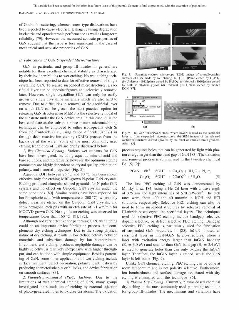
1) Wet Chemical Etching: Various wet etchants for GaNhave been investigated, including aqueous mineral acid andbase solutions, and molten salts; however, the optimum etchingparameters are highly dependent on crystal quality, orientation,polarity, and material properties (Fig. 8).
Aqueous KOH between 26 °C and 80 °C has been showneffective only for etching MBE-grown N-polar GaN crystals.Etching produced triangular-shaped pyramids for N-polar GaNcrystals and no effect on Ga-polar GaN crystals under thesame conditions [80]. Similar results have been reported forhot Phosphoric acid (with temperature > 200 °C), where onlydefect areas are etched on the Ga-polar GaN crystals, andshow hexagonal etch pits with an etch rate of ∼1 μm/min forMOCVD-grown GaN. No significant etching was observed fortemperatures lower than 160 °C [81], [82].
Although not very effective for patterning GaN, wet etchingcould be an important device fabrication process that com-plements dry etching techniques. Due to the strong physicalnature of dry etching, it results in low etch-selectivity betweenmaterials, and subsurface damage by ion bombardment.In contrast, wet etching, produces negligible damage, can behighly selective, is relatively inexpensive with higher through-put, and can be done with simple equipment. Besides pattern-ing of GaN, some other applications of wet etching includesurface treatment, defect decoration, polarity identification byproducing characteristic pits or hillocks, and device fabricationon smooth surfaces [83].
2) Photoelectrochemical (PEC) Etching: Due to thelimitations of wet chemical etching of GaN, many groupsinvestigated the stimulation of etching by external injectionof photo-generated holes to oxidize Ga atoms. The oxidation
Fig. 8. Scanning electron microscope (SEM) images of crystallographicsurfaces of GaN made by wet etching. (a) {1013}Plane etched by H3PO4.(b) Undercut {1012}plane etched by H3PO4. (c) Vertical {1010}plane etchedby KOH in ethylene glycol. (d) Undercut {1011}plane etched by moltenKOH [87].
Fig. 9. (a) GaN/InGaN/GaN stack, where InGaN is used as the sacrificiallayer to from suspended microstructures. (b) SEM images of the releasedcantilever structures curved upwards by the relief of intrinsic strain gradient.After [85].
process requires holes that can be generated by light with pho-ton energy larger than the band gap of GaN [83]. The oxidationand removal process is summarized in the two-step chemicalEq. (5) [2]:
2GaN + 6h+ + 6OH− → Ga2O3 + 3H2O + N2 ↑,
Ga2O3 + 6OH− → 2GaO−33 + 3H2O. (5)
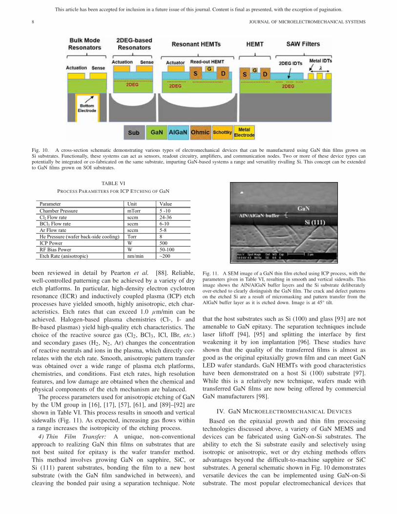
The first PEC etching of GaN was demonstrated byMinsky et al. [84] using a He–Cd laser with a wavelengthof 325 nm and light intensities of 570 mW/cm2. The etchrates were about 400 and 40 nm/min in KOH and HClsolutions, respectively. Selective PEC etching can also beused to form suspended structures by selective removal ofIII-nitride-based crystalline sacrificial layers. The techniquesused for selective PEC etching include bandgap selective,dopant selective, or defect selective PEC etching. Bandgapselective PEC etching is particularly used for fabricationof suspended GaN structures. In [85], InGaN is used assacrificial layer in InGaN/GaN hetero-structures, where alaser with excitation energy larger than InGaN bandgap(Eg = 3.0 eV) and smaller than GaN bandgap (Eg = 3.4 eV)is used to generate holes than can only oxidize the InGaNlayer. Therefore, the InGaN layer is etched, while the GaNlayer is left intact (Fig. 9).
Unlike GaN chemical etching, PEC etching can be done atroom temperature and is not polarity selective. Furthermore,ion bombardment and surface damage associated with dryetching is eliminated with this technique [86].
3) Plasma Dry Etching: Currently, plasma-based chemicaldry etching is the most commonly used patterning techniquefor group III-nitrides. The mechanisms and variations have
This article has been accepted for inclusion in a future issue of this journal. Content is final as presented, with the exception of pagination.
8 JOURNAL OF MICROELECTROMECHANICAL SYSTEMS
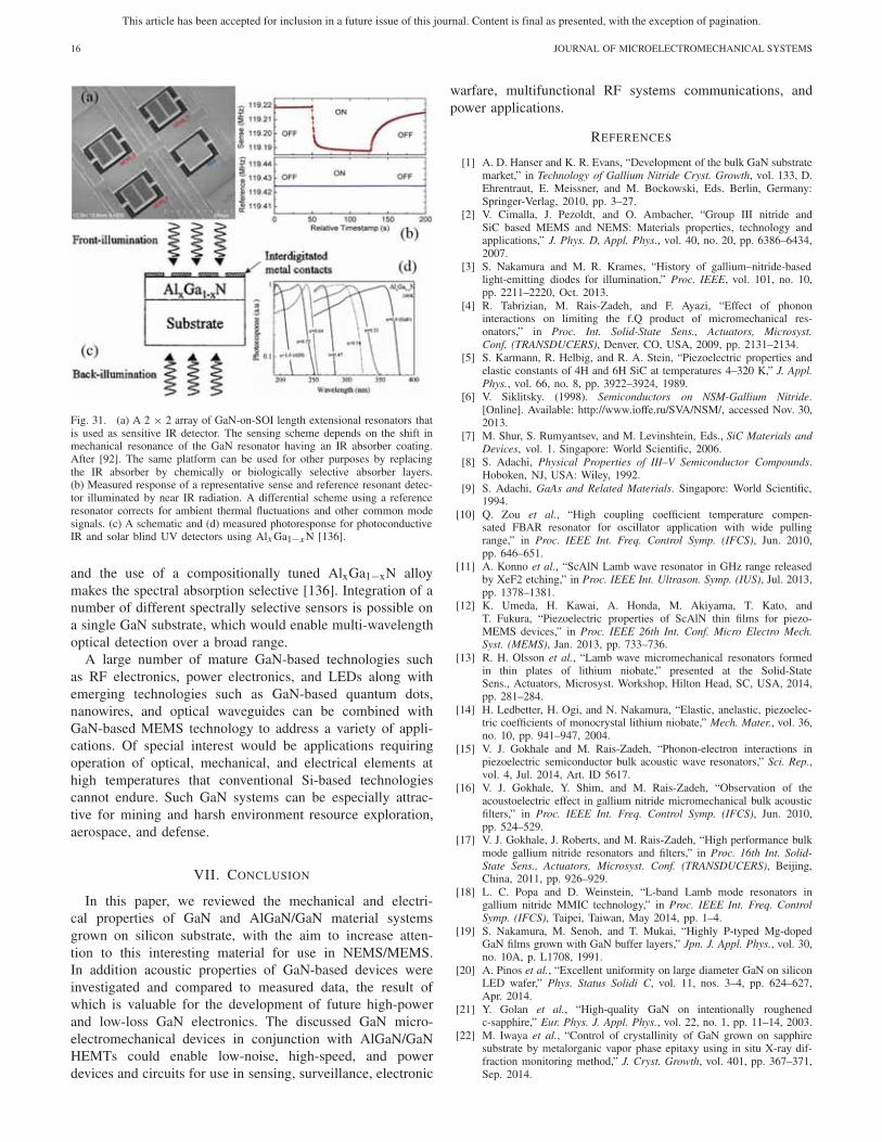
Fig. 10. A cross-section schematic demonstrating various types of electromechanical devices that can be manufactured using GaN thin films grown onSi substrates. Functionally, these systems can act as sensors, readout circuitry, amplifiers, and communication nodes. Two or more of these device types canpotentially be integrated or co-fabricated on the same substrate, imparting GaN-based systems a range and versatility rivalling Si. This concept can be extendedto GaN films grown on SOI substrates.
TABLE VI
PROCESS PARAMETERS FOR ICP ETCHING OF GaN
been reviewed in detail by Pearton et al. [88]. Reliable,well-controlled patterning can be achieved by a variety of dryetch platforms. In particular, high-density electron cyclotronresonance (ECR) and inductively coupled plasma (ICP) etchprocesses have yielded smooth, highly anisotropic, etch char-acteristics. Etch rates that can exceed 1.0 μm/min can beachieved. Halogen-based plasma chemistries (Cl-, I- andBr-based plasmas) yield high-quality etch characteristics. Thechoice of the reactive source gas (Cl2, BCl3, ICl, IBr, etc.)and secondary gases (H2, N2, Ar) changes the concentrationof reactive neutrals and ions in the plasma, which directly cor-relates with the etch rate. Smooth, anisotropic pattern transferwas obtained over a wide range of plasma etch platforms,chemistries, and conditions. Fast etch rates, high resolutionfeatures, and low damage are obtained when the chemical andphysical components of the etch mechanism are balanced.
The process parameters used for anisotropic etching of GaNby the UM group in [16], [17], [57], [61], and [89]–[92] areshown in Table VI. This process results in smooth and verticalsidewalls (Fig. 11). As expected, increasing gas flows withina range increases the isotropicity of the etching process.
4) Thin Film Transfer: A unique, non-conventionalapproach to realizing GaN thin films on substrates that arenot best suited for epitaxy is the wafer transfer method.This method involves growing GaN on sapphire, SiC, orSi (111) parent substrates, bonding the film to a new hostsubstrate (with the GaN film sandwiched in between), andcleaving the bonded pair using a separation technique. Note
Fig. 11. A SEM image of a GaN thin film etched using ICP process, with theparameters given in Table VI, resulting in smooth and vertical sidewalls. Thisimage shows the AlN/AlGaN buffer layers and the Si substrate deliberatelyover-etched to clearly distinguish the GaN film. The crack and defect patternson the etched Si are a result of micromasking and pattern transfer from theAlGaN buffer layer as it is etched down. Image is at 45° tilt.
that the host substrates such as Si (100) and glass [93] are notamenable to GaN epitaxy. The separation techniques includelaser liftoff [94], [95] and splitting the interface by firstweakening it by ion implantation [96]. These studies haveshown that the quality of the transferred films is almost asgood as the original epitaxially grown film and can meet GaNLED wafer standards. GaN HEMTs with good characteristicshave been demonstrated on a host Si (100) substrate [97].While this is a relatively new technique, wafers made withtransferred GaN films are now being offered by commercialGaN manufacturers [98].
IV. GaN MICROELECTROMECHANICAL DEVICES
Based on the epitaxial growth and thin film processingtechnologies discussed above, a variety of GaN MEMS anddevices can be fabricated using GaN-on-Si substrates. Theability to etch the Si substrate easily and selectively usingisotropic or anisotropic, wet or dry etching methods offersadvantages beyond the difficult-to-machine sapphire or SiCsubstrates. A general schematic shown in Fig. 10 demonstratesversatile devices the can be implemented using GaN-on-Sisubstrate. The most popular electromechanical devices that

This article has been accepted for inclusion in a future issue of this journal. Content is final as presented, with the exception of pagination.
RAIS-ZADEH et al.: GaN AS AN ELECTROMECHANICAL MATERIAL 9
Fig. 12. Representative SEM images (a, b) and RF transmission responses(c, d) of length-extensional mode GaN resonators. These devices workefficiently in the VHF and low-UHF range and can be used for timing andsensing applications. Multiple frequencies are possible on a single substrate.
have been implemented thus far using GaN-on-Si wafers aremicromechanical resonators and cantilevers. In the follow-ing subsections, we review a number of GaN-based devicesreported in the literature. In Section V, we extract some ofthe intrinsic properties of GaN (grown on Si) from the datapresented in this section.
A. Piezoelectric Actuation & Readout
Bulk acoustic wave (BAW) resonant devices made fromGaN have relied heavily on the piezoelectric properties of thematerial for actuation and readout. Piezoelectrically actuatedGaN resonators operating in various modes of resonance andacross a broad range of frequencies have been demonstrated bya number of research groups in the recent past. Popular imple-mentations of such devices are length- or width-extensionalresonators and thickness-mode resonators.
1) GaN Length-Extensional Mode Resonators: Length-extensional mode GaN resonators are mechanically releasedGaN plates tethered at specific nodal points. They are actu-ated by using the e31 coefficient of GaN by applying anRF signal across the thickness of the GaN film, causinglongitudinal vibrations in the frequency determining dimension(length or width). The distinct advantage of in-plane length-extensional mode resonators is that the significant dimension(and thus the resonant frequency) can be set lithographically,enabling multiple fundamental vibration modes on a singlesubstrate. Furthermore, the resonators can be operated athigher harmonics by using inter-digitated transducer (IDT) topelectrodes (Fig. 12). Length-extensional mode GaN resonatorshave been demonstrated in the recent past, with frequenciesin the VHF and low-UHF range from 4 MHz to more than400 MHz [17], [57], [90], [99], [100].
2) GaN Thickness-Extensional Mode Resonators: As withlength-extensional mode resonators, thickness-extensional
Fig. 13. (a) SEM and (b) de-embedded frequency response of thickness-extensional mode resonator, with a fourth-order thickness mode resonancefrequency of 8.69 GHz, exhibiting a Q of 330. Resonance frequency is setby the film thickness. These devices are generally designed to achieve higherfrequencies in the high-UHF to SHF spectrum [101].
Fig. 14. Similar to the GaN thin-film resonators, one can use GaN-on-Sicomposite structures to develop TPoS resonators. These resonators combinethe robustness and low acoustic loss of a thick Si layer with the efficientpiezoelectric actuation of GaN. One can design FBAR type (a, b) or IDTtype (c, d) filters using a GaN TPoS structures [89].
mode resonators are longitudinal BAW devices. The funda-mental resonance frequency is inversely proportional to thefilm thickness and the effective piezoelectric coefficient isthe larger e33 value. With GaN thin-films ranging from lessthan 1 μm to about 2 μm, resonators with frequencies up to8.7 GHz have been realized (Fig. 13) [101].
3) GaN-on-SOI Resonators: Both thickness-extensionalmode and length-extensional mode resonators can befabricated using GaN-on-SOI substrate in a (Fig. 14) TPoSconfiguration [63], [64]. Composite resonators have the advan-tage of combining the piezoelectric properties of GaN withthe acoustic properties of the substrate. In general, the thickercomposite stack allows for a more mechanically and thermallyrobust device. If the substrate layer is well doped Si, it canact as the bottom electrode. This eliminates the need for ametal electrode with a large acoustic mismatch with GaN.The use of GaN-on-SOI substrates can be explored in thefuture for heterogeneous integration of GaN- and Si-basedelectromechanical devices and readout/signal processingcircuitry on the same substrate.

This article has been accepted for inclusion in a future issue of this journal. Content is final as presented, with the exception of pagination.
10 JOURNAL OF MICROELECTROMECHANICAL SYSTEMS
Fig. 15. (a) GaN cantilever structures (From [103]) and (b) GaN nanowires(From [107]) can be used as sensing elements utilizing the piezoresistiveeffect in AlGaN/GaN 2DEG sheet. The high gauge factor of AlGaN/GaNis due to the large modulation of the electronic properties of GaN andAlGaN due to strain. Another major advantage of GaN piezoresistors is theability to work at significantly elevated temperatures and still retain a highsensitivity.
B. Piezoresistive Sensing and Readout
Mechanical devices based on the GaN/AlGaN system canbe used as highly sensitive piezoresistive sensors for detect-ing small amounts of static or dynamic strain [102]–[105].Strain applied to mechanically released, flexural-mode micro-cantilevers modulates the piezoelectric polarization at theGaN/AlGaN interface [104] as well as the carrier mobilitydue to strain-induced band-bending [105], [106]. Both effectslead to large detectable changes in the instantaneous resistance.These changes can be sensed by simple readout circuits orby using an integrated 2DEG-based transistor (Fig. 15(a)).Gauge factors (the relative change in resistance with respectto change in strain) as high as 3532 [103] have been reportedfor such structures. This is in comparison to the significantlylower numbers reported for Si [103]. GaN/AlGaN piezore-sistive systems are expected to maintain high gauge factorseven at elevated temperatures, beyond the working rangeof conventional semiconductor piezoresistors, thus makingthem attractive candidates for harsh environment sensing.The piezoresistive effect has also been used as a readoutmechanism for GaN nanowire based mechanical resonators(Fig. 15(b)) [107].
C. 2DEG Electrodes
As mentioned earlier, a 2DEG sheet is induced at theAlGaN/GaN interface due to the spontaneous and piezoelectricpolarization. The origin of 2DEG, unlike the conductingchannel in Si transistors, suggests that they are very sensitiveto mechanical stress, changing the piezoelectric polarization-induced surface and interface charges. Furthermore, 2DEG issensitive to other environmental influences, such as tempera-ture, illumination, or chemical surface modifications. Since the2DEG is formed very close to the surface (typically ∼30 nmbelow the surface), it is highly sensitive to surface potentials.2DEG has been shown in sensor applications such as pH,viscosity, mass, and a variety of other novel sensor conceptsare conceivable based on its properties. Moreover, 2DEG canreplace metal electrodes in piezoelectric resonators. 2DEGconductive sheet, inherent to the AlGaN/GaN piezoelectric
Fig. 16. (a) Schematic and (b) frequency response of a piezo-electrically actuated AlGaN/GaN resonator using 2DEG as the bottomelectrode [110].
Fig. 17. Actuation efficiency versus bias voltage of an AlGaN actuator wherea 2DEG is used as bottom electrode. After [111].
material system can effectively reduce the metal loading andacoustic mismatch associated with metal electrode deposition,and thus improve the resonator performance. It can either beutilized as the top or bottom electrode in MEMS for actuationas well as readout. A summary of GaN-based resonant deviceswith embedded 2DEG electrodes, as well as a class of resonantdevices, i.e. “Resonant HEMTs,” based on 2DEG sensing isprovided in the following subsections.
1) 2DEG Bottom Electrode: The 2DEG at the AlGaN/GaN-interface can be utilized as the bottom electrode for piezoelec-tric actuation and read-out of AlGaN/GaN suspended beams(Fig. 16). The elimination of bottom electrode metallization isparticularly beneficial in GaN-based resonators since singlecrystalline GaN cannot be directly grown on metal sheets.Implementation of 2DEG as the bottom electrode was demon-strated in [100] and [108]–[110], where resonant frequenciesof up to 60 MHz with a maximum frequency times Q ( f ×Q)value of 9.42 × 19 have been reported for longitudinal- andflexural-mode resonators.
The main difference between using metal-piezo-2DEGinstead of the known metal-piezo-metal structures is that thein the case of 2DEG the actuation amplitude is bias dependentand drops below the pinch-off voltage [111] (Fig. 17). Never-theless, the actuation remains non-negligible at lower negativebiases. This is due to the remaining field distribution insidethe piezoelectric GaN buffer.
2) Patterned 2DEG as Top Electrode: In order to reducethe mass loading associated with the deposition of metalas the top electrode on piezoelectric resonators, severalapproaches have been taken. In AlN piezoelectric resonators,

This article has been accepted for inclusion in a future issue of this journal. Content is final as presented, with the exception of pagination.
RAIS-ZADEH et al.: GaN AS AN ELECTROMECHANICAL MATERIAL 11
Fig. 18. (a) A SEM of 2DEG IDT resonator. The 2DEG electrodes arepatterned with a 90 nm deep AlGaN etch. (b) Mode shape showing the strainfields induced at resonance. (c) De-embedded frequency response of 1.22 GHz2DEG IDT resonator. After [58].
Fig. 19. (a) optical image, (b) a SEM image, and (c) measurement setup of aflexural-mode Resonant HEMT. (d) Amplification of mechanical transductioninside the HEMT integrated on the flexural beam [115].
efforts have included physically separating electrodes from thepiezoelectric thin film [112] and segmentation of IDT metalelectrodes [113]. GaN material systems benefit from the2DEG conductive sheet, which can be used to define elec-trodes and thus completely remove metal from the reso-nant structure. In [58], a metal-free piezoelectric resonatorsis presented, which utilizes 2DEG IDTs to drive acousticwaves in an AlGaN/GaN hetero-structure (Fig. 18). Metal-free acoustic filters, with patterned 2DEG electrodes had beenpreviously reported in AlGaN/GaN SAW filters discussedin Section E.
D. AlGaN/GaN Resonant HEMTs
Resonant AlGaN/GaN HEMTs exploit the high sensitivityof the HEMT 2DEG conducting channel to the acoustic straininduced by an actuator in a resonant cavity on which theHEMT is fabricated. As mentioned earlier, the 2DEG sheetis very sensitive to mechanical stress. A small change instress translates into a considerable change in 2DEG carrierconcentration, which is in turn sensed though the change in theHEMT drain current. 2DEG sensitivity to mechanical stresshas been widely used in static AlGaN/GaN strain sensors anddiscussed in detail in the literature [114]. In the resonantHEMTs, the acoustic wave is launched into the resonantdevice, for example by an additional Schottky contact forpiezoelectric excitation, and sensed through detection of a peakin the frequency response of the HEMT drain current at res-onance. Using HEMT-based read-out, capacitive feed-throughis reduced allowing for operation at higher frequencies. Alsohigher sensitivity and signal amplification is achieved due to
Fig. 20. (a) (Top) SEM image and (bottom) measured frequency responseof a passive resonator in air. (b) (Top) SEM image and (bottom) frequencyresponse of a piezoelectric drive, HEMT-sensed resonator [59].
inherent gain in the HEMT. Resonant HEMTs are discussed inthe next section and categorized by their mode of resonance,i.e. flexural, longitudinal, and thickness mode. They are allfabricated on GaN-on-Si substrates.
1) Flexural-Mode Resonant HEMTs: AlGaN/GaN resonantHEMTs were first demonstrated in [115], where flexuralmode acoustic resonance was excited and sensed on a doublyclamped beam using Schottky diodes for excitation and HEMTtransducers for read-out (Fig. 19).
Working at 1.49 MHz with a Q of 1850, the device wasoperated at different drain and gate biases. This enabledthe observation of intrinsic amplification of the mechanicaltransduction (Fig. 19). Moreover, a detailed study based onthe same kind of devices [113] confirmed that the response isdriven by the 2DEG mobility under the gate and in the accessregions. A quantitative model was proposed to account for thetransconductance variations that have strong similarities withtransconductance curves usually recorded on such transistors.
2) Width-Extensional Mode R-HEMTs: Bulk acousticwidth-extensional mode resonant HEMTs have been reportedin [59] and compared with passive AlGaN/GaN resonatorsusing 2DEG as the bottom electrode. Resonance frequenciesranging from 240 MHz to 3.5 GHz with Q values of upto ∼500 are reported in air. Fig. 20 compares a passiveAlGaN/GaN resonator with a width-extensional resonatorreadout using an active HEMT. In Fig. 20(a), the HEMTprovides electromechanical amplification of the mechanicalsignal, enabling sensing at much higher frequencies thanpossible with passive devices.
3) Thickness-Extensional Mode R-HEMTs: A multi-gigahertz thickness mode AlGaN/GaN resonant HEMTis reported in [61] and [91], where the vertical electricalfield excites the thickness-mode acoustic resonance of aresonating stack through the thickness-mode piezoelectriccoefficient (e33). Acoustic signal is excited through a backgate Schottky contact and read-out by measuring the draincurrent of the sense HEMT. The back gate and the senseHEMT channel are placed at locations under maximumstrain. The source is placed at a nodal point and tied to GND.

This article has been accepted for inclusion in a future issue of this journal. Content is final as presented, with the exception of pagination.
12 JOURNAL OF MICROELECTROMECHANICAL SYSTEMS
Fig. 21. (a) Schematic view of an AlGaN/GaN thickness-mode resonantHEMT. AC signal is applied to the back gate that is biased in the depletionregion and picked up by sensing the drain current. (b) SEM images ofthe fabricated device. (c) Measured acoustic transconductance, showing aresonance peak only when the actuator is biased in depletion [91].
Fig. 22. (a) Schematic and transmission response of GaN-on-sapphire SAWfilter, after [117]. Two peaks are observed in the 0-3 GHz frequency range, at1.6 GHz and 2.2 GHz, associated with Rayleigh and Love waves respectively.(b) SEM images and transmission response of GaN-on-Si SAW filters, with200 nm spacing (λ = 0.8 μm), and a 5.6 GHz resonance frequency [118].
The device shows the second-order resonance frequencyof 4.23 GHz with a Q of 250 (Fig. 21). The acoustictransconductance (ga) rises to ∼25 μS when the transduceris ON. Co-integrated with GaN ICs, this resonant HEMT canpotentially offer all-GaN integrated nano/micro sensors andsystems. The resonance frequency can be further increased byexciting higher harmonics of the thickness-mode resonance.This device exhibits the highest resonance frequency reportedthus far for a resonant HEMT.
E. SAW Filters
SAW devices have been traditionally fabricated on quartz,ZnO, LiTaO3, and LiNbO3 [116] and used in a variety ofsensing and communication applications. The III-nitride fam-ily combines a high SAW velocity and electromechanical cou-pling coefficient with excellent thermal and chemical stability.All these properties are of high interest for the developmentof SAW devices operating at frequencies higher than 1 GHz,a common requirement of most modern telecommunicationapplications [117].
Fig. 23. (a) Schematic of the SAW filter with 2DEG IDTs onAlGaN/GaN/Sapphire structure. (b) Frequency responses of the SAW filterswith metal-metal, metal-2DEG, and 2DEG-2DEG IDTs [119].
In [117], SAW filters with resonant frequencies ofup to 2.22 GHz were realized on GaN-on-sapphire substrate,with 600 nm wide fingers and inter-digit spacing (Fig. 22(a)).More recently, a 5.6 GHz SAW filter, with 200 nm widefingers and inter-digit spacing was realized on GaN-on-Si sub-strate (Fig. 22(b)), marking the highest resonance frequencyachieved for GaN SAW resonators to date [118].
SAW filters using 2DEG IDT on AlGaN/GaN hetero-structure are demonstrated in [119] based on a fluoride-based (CF4) plasma treatment technique. The CF4 plasmatreatment is used to pattern 2DEG IDT on a planar surfacewithout removing the top AlGaN layer (Fig. 23(a)). SAWpeaks correspond to the Rayleigh and pseudo-bulk modesof the epitaxial structure. The Rayleigh mode is primarilyconfined to the thin-film epitaxy, while the pseudo-bulk modeis primarily confined to the sapphire substrate near its interfacewith GaN. The frequency range of the fabricated SAW filtersis between 400 MHz and 1.2 GHz (Fig. 23(b)).
In [120], 2DEG-based SAW filters are integrated withHEMT structures to study the emission of SAWs byAlGaN/GaN HEMTs under certain bias conditions. IDT-IDTand HEMT-IDT pairs are compared for SAW emission anddetection. Integrated HEMT-IDT structures can enable real-time evaluation of epitaxial degradation as well as high-speed,amplified detection of SAWs.
F. Integrated Circuits With MEMS Resonatorsand HEMTs
GaN microsystems take advantage of integration of GaNmechanical components with GaN HEMTs. As mentionedearlier, GaN HEMTs are being widely used in RF poweramplifiers. There is a great demand for miniaturization ofsuch products and designers continuously move from hybrid(circuit board with discrete components) to integrated (single,small chip) more compact solutions. Integrated microsystemsoffer higher densities, added functionality, and suffer lessfrom parasitics associated with wire-bonding or other hybridsolutions. One of the applications of integrated GaN materialsystems is MEMS-based oscillators. MEMS oscillators arecritical in building all-integrated accurate timing referencesand frequency-stable circuits. Low phase noise, temperaturestable MEMS oscillators operable at harsh environments withhigh resonance frequencies and significant delivered out-put powers are achievable in GaN integrated microsystems.Despite of their great promise, few reports exist on imple-mentation of an all-GaN oscillator, where a GaN resonator is

This article has been accepted for inclusion in a future issue of this journal. Content is final as presented, with the exception of pagination.
RAIS-ZADEH et al.: GaN AS AN ELECTROMECHANICAL MATERIAL 13
Fig. 24. (a) SEM image and (b) schematic, (c) frequency response ofintegrated cascade of a resonator and HEMT. The insertion loss is modulatedby more than 10 dB [60].
utilized for frequency selectivity and an AlGaN/GaN HEMTprovides gain for building up oscillation. Below, we reviewthe two recent structures that integrated GaN resonators andAlGaN/GaN HEMTs.
1) Integrated Bulk-Mode GaN Resonators and HEMTs:In [60], a platform for monolithic integration of GaN BAWresonators and HEMTs is shown (Fig. 24). The output port ofthe resonator is connected to the gate of the transistor, wherethe signal gets amplified by the intrinsic gain of the transistorand picked up at the drain. This platform provides the mainbuilding block of a Pierce oscillator circuit, where the feedbackloop is formed by simply connecting the resonator input to theHEMT drain.
2) GaN SAW Oscillator: In [121], a SAW device has beenincorporated in a feed-back loop with an off-the-shelf amplifierto build an all-GaN oscillator (Fig. 25). The SAW filter showsa Q of 1730 at a resonance frequency of ∼1 GHz. A phasenoise of −115 dBc/Hz was recorded at 10 kHz offset from thecarrier with noise floor of −165 dBc/Hz. Several tracks arecurrently considered to improve the Q of the resonator andhence the phase noise figure of merit.
V. PERFORMANCE METRICS FOR
GaN RESONANT DEVICES
A. Quality Factor and f × Q Limits
One of the most important metrics for mechanical resonatorsis the product of frequency and Q. The Q of an acousticresonator is directly related to the total energy lost, whichis quantified by the attenuation coefficient, as discussed inSection II-G. While extrinsic energy loss to the ambientmedia (damping and anchor loss) can be reduced by vacuumpackaging and using a good design, energy lost as heat(thermoelastic damping), intrinsic energy losses to the materiallattice (phonon-phonon loss), and energy lost to conductionelectrons (phonon-electron loss) are considered the ultimatelimiting factors of the resonator Q. The measured values ofthe resonator f ×Q are a good indicator of how close theresonator is to the limiting values. If the acoustic wave isconsidered as a strain wave in the material, at a frequency thatis much lower than the inverse of the lattice relaxation timeof the material crystalline structure, it is found theoretically
Fig. 25. (a) Frequency response of a double-port SAW resonator. Inset showsthe SEM image of the resonator built on GaN-on-Si (111). (b) Experimentaloscillator setup, including the packaged resonator, a low noise integratedamplifier, a phase-shifter and a coupler [121].
Fig. 26. Calculated values of the f ×Q limits for the dominant intrinsic dissi-pation mechanisms in GaN. Measured results (with error bar) from [17], [18],[58]–[60], [101], and [125].
that the product of frequency and the limiting material Qremains constant (across frequency) [4]. This is known as theAkhieser f ×Q limit. For GaN, this regime should be valid forfrequencies as high as 5 GHz. Above this value, the system canbe treated as an ensemble of phonons and the limiting valuesof f ×Q is given by the Landau–Rumer (L–R) regime. Forhigh-frequency longitudinal wave resonators made from GaN,the thermoelastic damping is not significant [122], however,it is generally a dominant damping mechanism for lower-frequency flexural-mode resonators [123], [124]. For GaN,a semiconductor, the electron scattering is also a significantloss mechanism and is highly dependent on the free carrierconcentration, the carrier mobility and the coupling betweenthe electrical and mechanical domains (due to piezoelectric ordeformation potential coupling) [73].
Fig. 26 shows the f ×Q limit of GaN due to differentloss mechanisms and compares that to the measured data(red circles) from GaN resonators presented in the previ-ous sections. The gap between the theoretical and mea-sured results is due to other effects that also play a rolein damping the device. It can be seen that the measured

This article has been accepted for inclusion in a future issue of this journal. Content is final as presented, with the exception of pagination.
14 JOURNAL OF MICROELECTROMECHANICAL SYSTEMS
Fig. 27. Measured values of (a) k2e f f as a function of and (b) k2
ef f × Q asa function of frequency. Data are taken from prior literature [17], [58]–[60].
f ×Q values are in the same order of magnitude as themaximum possible f ×Q limit even using GaN grown onSi. The exact values are dependent on the quality of theGaN film, the carrier concentration of GaN used, and thespecific design of the resonator. However, in general, higher-frequency resonators have shown better performance in termsof f ×Q values.
B. Coupling Efficiency and the k2e f f × Q Metric
The piezoelectric coupling coefficient k2t is a material
property that determines the efficiency of converting electri-cal energy into mechanical energy and vice-versa. For thevarious electromechanical axes of GaN, the values of k2
trange from 1.3% for in-plane modes to ∼2% for thicknessmodes [6], [126]. The effective coupling coefficient k2
e f f isextracted from the mechanical response of the resonatorsand includes the effects of metal electrode loading, non-idealelectrode area coverage, and anisotropic effects [126]. Themeasured values of k2
e f f in prior literature (Fig. 27(a)) areseen to be close to the calculated maximum values for boththe thickness modes (measured to be ∼1.9%) and in-planemodes (measured to be up to ∼0.9%).
Another related metric that is used often for characteriz-ing the applicability of a piezoelectric material for use inRF electromechanical filters is the k2
e f f ×Q product. Practi-cally, a higher resonator k2
e f f increases the separation betweenthe series and parallel resonances. For coupled-resonator filtertopologies, this higher separation implies a wider bandwidth.A higher Q (for each individual resonator) imparts a sharperroll-off for the filter. Thus, a high k2
e f f ×Q product is desirablefor wide-band RF filters [126]. In this regard, measured GaNresonators have demonstrated similar numbers (Fig. 27(b)) incomparison with quartz, diamond, TPoS and Si-based internaldielectric transduction. However, it is significantly lower thanstronger piezoelectric materials such as LiNbO3 [127], orhighly optimized devices such as the AlN FBARs [128].We believe that the consistent and rapid improvements in thereported k2
e f f × Q of GaN resonators indicate that there is yetroom for improvement.
TABLE VII
A COMPARISON BETWEEN RESONANCE FREQUENCY, Q, AND
TRANSCONDUCTANCE (ga ) OF Si AND GaN-BASED
RESONANT TRANSISTORS
C. Acoustic Transconductance
Acoustic transconductance is a figure of merit specificallyused in resonant FET-based sensing, which reflects the changesin the drain current of the transistor, when there is a change inthe voltage applied to an actuator. An AC voltage applied to theactuator causes acoustic strain in the resonant structure, whichin turn, changes the drain current of the transistor. Therefore,one can define a new transconductance parameter, i.e. acoustictransconductance as:
ga = d(I D)
d (VBG), (6)
where ga is the acoustic transconductance, d(I D) is theamplitude of the drain AC current and d (VBG) is the ampli-tude of the AC voltage applied to the actuator port (e.g.,a back gate Schottky contact). ga is extracted from theadmittance matrix of the resonant HEMT, similar to theextraction procedure of the transconductance of any standardtransistor as:
ga = |Y 21 − Y12| (7)
Table VII compares the resonance frequencies, Qs, andthe acoustic transconductance values of Si resonant transis-tors and AlGaN/GaN resonant HEMTs, extracted from the|Y21-Y12| curves.
D. Temperature Coefficient of Frequency
One of the important metrics for resonator performanceis the temperature coefficient of frequency (TCF), whichdescribes the relative shift in the resonator frequency withtemperature change. The TCF is a function of the materialproperties, resonator mode, and dimensions of the device.In most materials, the dominant mechanism is the change inthe elastic modulus of the material with respect to temper-ature, defined by temperature coefficient of elasticity (TCE).For many mechanical resonator applications, such as oscil-lators, clocks and gyroscopes, the objective is to minimizethe TCF in order to get temperature invariant performance.For thermal and infrared (IR) sensors [57], [90], [92], thetemperature dependency should be maximized. In both cases,it is important to carefully characterize the TCF of the

This article has been accepted for inclusion in a future issue of this journal. Content is final as presented, with the exception of pagination.
RAIS-ZADEH et al.: GaN AS AN ELECTROMECHANICAL MATERIAL 15
Fig. 28. The change in the frequency of two length-extensional GaNresonators as a function of temperature, showing a negative TCF withexperimentally measured values of between −14 ppm/K to −18 ppm/K [16],[17], [89], [90].
resonator. Theoretical calculations for the stiffness coeffi-cients of GaN [133] indicate TCE values of −50 ppm/Kto −54 ppm/K for longitudinal extension. TCF should beroughly half of that value for extensional resonators since itis the dominant mechanism for frequency change. For theGaN resonators measured by the authors at the Universityof Michigan, the TCF values for length-extensional modesrange from −14 ppm/K to −18 ppm/K [16], [17], [89], [90].TCF values ranging from −23 ppm/K to −25 ppm/K arereported for thickness-extensional mode resonances of thedevices reported in [16], [17], [89], and [90]. Larger TCFvalues of −27.6 ppm/K and −30 ppm/K are reported in [134]for thickness-extensional modes at resonance frequencies of2.2 GHz and 8.7 GHz respectively. The larger measured TCFin [134] is most likely due to the thicker AlN and metal layersin the resonant stack with a larger TCE as compared to GaN.Also, specific material properties in different stacks (e.g., dif-ferent level of doping for unintentionally doped GaN) cancause variations in measured TCF values. Representative plotsof the TCF for two fabricated length-extensional resonators areshown in (Fig. 28).
E. Power Handling and IIP3
The ability to handle high power levels has always been oneof the most attractive features of GaN-based electronics. Thishas spurred the growth of a large power-electronics industry.Electromechanical devices, especially resonators, also havelimiting values of input power that can be handled withoutdistortion of the output due to the onset of electrical andmechanical non-linearity. In piezoelectric resonators, mechan-ical non-linearity is primarily due to the non-linearity inthe elastic coefficients of the material (especially for thesuspension tethers) [62]. A popular method for characterizingthe non-linearity and distortion of mechanical resonators asso-ciated with high input power levels is the third order interceptpoint (IIP3). For GaN length-extensional mode resonators withthin tethers, distortion is seen at +5 dBm or greater, whileno distortion is seen for clamped membrane type thickness-mode resonators at input powers up to +20 dBm [17].Extrapolated IIP3 (Fig. 29) demonstrate values in excess of+32 dBm without requiring the use of thick silicon structural
Fig. 29. Measured IIP3 for a GaN mechanical resonator. The data aremeasured on a 2.1 GHz with a frequency separation of 50 kHz. The measuredGaN bulk acoustic wave resonator shows Q of ∼500.
Fig. 30. A simplified schematic of a front-end transmitter based on all-GaNmodules.
layers in the device, a method that is used in the AlN-on-SiTPoS configuration [62]. These values are comparable withsimilar devices made using AlN [135].
VI. FUTURE POSSIBILITIES
All-GaN integrated microsystems benefit from the combinedadvantages of piezoelectric properties of GaN for sensing andactuation and inherent gain in the AlGaN/GaN HEMTs forsignal amplification. In fact, integrated circuits with diversefunctionalities can be realized based on electromechanicalproperties of GaN. GaN HEMTs and MEMS components,co-integrated with high-Q passives, such as capacitors andinductors can be used in timing and sensing applications. As anexample of a critical application of integrated GaN microsys-tem, a simple transmitter MMIC schematic is shown in Fig. 30,where the preferred integration boundary of the power ampli-fier and other front-end components are demonstrated. GaNmonolithic microwave integrated circuits (MMICs) providebetter performance in terms of power, radiation hardness,and operation temperature, leading to products that could beused in harsh environments. Furthermore, future integrationwith GaN optoelectronic components is possible to incorporatediverse functionalities on the same GaN system.
GaN resonant systems can be used for a variety of physical,chemical, and biological sensing applications. Resonant IRdetector arrays using GaN and GaN-on-Si structures have beendemonstrated recently [57], [90], [92] (Fig. 31(a, b)) and havethe potential to achieve highly sensitive IR detection with lowsusceptibility to background thermal noise. The same platformcan be used for detecting small perturbations in temperatureor mass. The wide bandgap of GaN also makes it a naturalcandidate for short wavelength optical detectors (Fig. 31(c, d)),
This article has been accepted for inclusion in a future issue of this journal. Content is final as presented, with the exception of pagination.
16 JOURNAL OF MICROELECTROMECHANICAL SYSTEMS
Fig. 31. (a) A 2 × 2 array of GaN-on-SOI length extensional resonators thatis used as sensitive IR detector. The sensing scheme depends on the shift inmechanical resonance of the GaN resonator having an IR absorber coating.After [92]. The same platform can be used for other purposes by replacingthe IR absorber by chemically or biologically selective absorber layers.(b) Measured response of a representative sense and reference resonant detec-tor illuminated by near IR radiation. A differential scheme using a referenceresonator corrects for ambient thermal fluctuations and other common modesignals. (c) A schematic and (d) measured photoresponse for photoconductiveIR and solar blind UV detectors using Alx Ga1−x N [136].
and the use of a compositionally tuned AlxGa1−xN alloymakes the spectral absorption selective [136]. Integration of anumber of different spectrally selective sensors is possible ona single GaN substrate, which would enable multi-wavelengthoptical detection over a broad range.
A large number of mature GaN-based technologies suchas RF electronics, power electronics, and LEDs along withemerging technologies such as GaN-based quantum dots,nanowires, and optical waveguides can be combined withGaN-based MEMS technology to address a variety of appli-cations. Of special interest would be applications requiringoperation of optical, mechanical, and electrical elements athigh temperatures that conventional Si-based technologiescannot endure. Such GaN systems can be especially attrac-tive for mining and harsh environment resource exploration,aerospace, and defense.
VII. CONCLUSION
In this paper, we reviewed the mechanical and electri-cal properties of GaN and AlGaN/GaN material systemsgrown on silicon substrate, with the aim to increase atten-tion to this interesting material for use in NEMS/MEMS.In addition acoustic properties of GaN-based devices wereinvestigated and compared to measured data, the result ofwhich is valuable for the development of future high-powerand low-loss GaN electronics. The discussed GaN micro-electromechanical devices in conjunction with AlGaN/GaNHEMTs could enable low-noise, high-speed, and powerdevices and circuits for use in sensing, surveillance, electronic
warfare, multifunctional RF systems communications, andpower applications.
REFERENCES
[1] A. D. Hanser and K. R. Evans, “Development of the bulk GaN substratemarket,” in Technology of Gallium Nitride Cryst. Growth, vol. 133, D.Ehrentraut, E. Meissner, and M. Bockowski, Eds. Berlin, Germany:Springer-Verlag, 2010, pp. 3–27.
[2] V. Cimalla, J. Pezoldt, and O. Ambacher, “Group III nitride andSiC based MEMS and NEMS: Materials properties, technology andapplications,” J. Phys. D, Appl. Phys., vol. 40, no. 20, pp. 6386–6434,2007.
[3] S. Nakamura and M. R. Krames, “History of gallium–nitride-basedlight-emitting diodes for illumination,” Proc. IEEE, vol. 101, no. 10,pp. 2211–2220, Oct. 2013.
[4] R. Tabrizian, M. Rais-Zadeh, and F. Ayazi, “Effect of phononinteractions on limiting the f.Q product of micromechanical res-onators,” in Proc. Int. Solid-State Sens., Actuators, Microsyst.Conf. (TRANSDUCERS), Denver, CO, USA, 2009, pp. 2131–2134.
[5] S. Karmann, R. Helbig, and R. A. Stein, “Piezoelectric properties andelastic constants of 4H and 6H SiC at temperatures 4–320 K,” J. Appl.Phys., vol. 66, no. 8, pp. 3922–3924, 1989.
[6] V. Siklitsky. (1998). Semiconductors on NSM-Gallium Nitride.[Online]. Available: http://www.ioffe.ru/SVA/NSM/, accessed Nov. 30,2013.
[7] M. Shur, S. Rumyantsev, and M. Levinshtein, Eds., SiC Materials andDevices, vol. 1. Singapore: World Scientific, 2006.
[8] S. Adachi, Physical Properties of III–V Semiconductor Compounds.Hoboken, NJ, USA: Wiley, 1992.
[9] S. Adachi, GaAs and Related Materials. Singapore: World Scientific,1994.
[10] Q. Zou et al., “High coupling coefficient temperature compen-sated FBAR resonator for oscillator application with wide pullingrange,” in Proc. IEEE Int. Freq. Control Symp. (IFCS), Jun. 2010,pp. 646–651.
[11] A. Konno et al., “ScAlN Lamb wave resonator in GHz range releasedby XeF2 etching,” in Proc. IEEE Int. Ultrason. Symp. (IUS), Jul. 2013,pp. 1378–1381.
[12] K. Umeda, H. Kawai, A. Honda, M. Akiyama, T. Kato, andT. Fukura, “Piezoelectric properties of ScAlN thin films for piezo-MEMS devices,” in Proc. IEEE 26th Int. Conf. Micro Electro Mech.Syst. (MEMS), Jan. 2013, pp. 733–736.
[13] R. H. Olsson et al., “Lamb wave micromechanical resonators formedin thin plates of lithium niobate,” presented at the Solid-StateSens., Actuators, Microsyst. Workshop, Hilton Head, SC, USA, 2014,pp. 281–284.
[14] H. Ledbetter, H. Ogi, and N. Nakamura, “Elastic, anelastic, piezoelec-tric coefficients of monocrystal lithium niobate,” Mech. Mater., vol. 36,no. 10, pp. 941–947, 2004.
[15] V. J. Gokhale and M. Rais-Zadeh, “Phonon-electron interactions inpiezoelectric semiconductor bulk acoustic wave resonators,” Sci. Rep.,vol. 4, Jul. 2014, Art. ID 5617.
[16] V. J. Gokhale, Y. Shim, and M. Rais-Zadeh, “Observation of theacoustoelectric effect in gallium nitride micromechanical bulk acousticfilters,” in Proc. IEEE Int. Freq. Control Symp. (IFCS), Jun. 2010,pp. 524–529.
[17] V. J. Gokhale, J. Roberts, and M. Rais-Zadeh, “High performance bulkmode gallium nitride resonators and filters,” in Proc. 16th Int. Solid-State Sens., Actuators, Microsyst. Conf. (TRANSDUCERS), Beijing,China, 2011, pp. 926–929.
[18] L. C. Popa and D. Weinstein, “L-band Lamb mode resonators ingallium nitride MMIC technology,” in Proc. IEEE Int. Freq. ControlSymp. (IFCS), Taipei, Taiwan, May 2014, pp. 1–4.
[19] S. Nakamura, M. Senoh, and T. Mukai, “Highly P-typed Mg-dopedGaN films grown with GaN buffer layers,” Jpn. J. Appl. Phys., vol. 30,no. 10A, p. L1708, 1991.
[20] A. Pinos et al., “Excellent uniformity on large diameter GaN on siliconLED wafer,” Phys. Status Solidi C, vol. 11, nos. 3–4, pp. 624–627,Apr. 2014.
[21] Y. Golan et al., “High-quality GaN on intentionally roughenedc-sapphire,” Eur. Phys. J. Appl. Phys., vol. 22, no. 1, pp. 11–14, 2003.
[22] M. Iwaya et al., “Control of crystallinity of GaN grown on sapphiresubstrate by metalorganic vapor phase epitaxy using in situ X-ray dif-fraction monitoring method,” J. Cryst. Growth, vol. 401, pp. 367–371,Sep. 2014.

This article has been accepted for inclusion in a future issue of this journal. Content is final as presented, with the exception of pagination.
RAIS-ZADEH et al.: GaN AS AN ELECTROMECHANICAL MATERIAL 17
[23] S. Q. Zhou, A. Vantomme, B. S. Zhang, H. Yang, and M. F. Wu,“Comparison of the properties of GaN grown on complex Si-basedstructures,” Appl. Phys. Lett., vol. 86, no. 8, p. 081912, 2005.
[24] A. Watanabe, T. Takeuchi, K. Hirosawa, H. Amano, K. Hiramatsu, andI. Akasaki, “The growth of single crystalline GaN on a Si substrateusing AIN as an intermediate layer,” J. Cryst. Growth, vol. 128,nos. 1–4, pp. 391–396, 1993.
[25] N. Baron et al., “The critical role of growth temperature on the struc-tural and electrical properties of AlGaN/GaN high electron mobilitytransistor heterostructures grown on Si(111),” J. Appl. Phys., vol. 105,no. 3, pp. 033701-1–033701-8, 2009.
[26] A. Soltani et al., “Assessment of transistors based on GaN on siliconsubstrate in view of integration with silicon technology,” Semicond.Sci. Technol., vol. 28, no. 9, p. 094003, 2013.
[27] H. P. D. Schenk, E. Frayssinet, A. Bavard, D. Rondi, Y. Cordier,and M. Kennard, “Growth of thick, continuous GaN layers on 4-in.Si substrates by metalorganic chemical vapor deposition,” J. Cryst.Growth, vol. 314, no. 1, pp. 85–91, 2011.
[28] A. Polian, M. Grimsditch, and I. Grzegory, “Elastic constants ofgallium nitride,” J. Appl. Phys., vol. 79, no. 6, pp. 3343–3344,1996.
[29] J. Kolník, I. H. Oguzman, K. F. Brennan, R. Wang, P. P. Ruden,and Y. Wang, “Electronic transport studies of bulk zincblende andwurtzite phases of GaN based on an ensemble Monte Carlo calculationincluding a full zone band structure,” J. Appl. Phys., vol. 78, no. 2,pp. 1033–1038, 1995.
[30] A. F. Wright, “Elastic properties of zinc-blende and wurtzite AlN, GaN,and InN,” J. Appl. Phys., vol. 82, no. 6, pp. 2833–2839, 1997.
[31] M. Yamaguchi et al., “Brillouin scattering study of gallium nitride:Elastic stiffness constants,” J. Phys., Condens. Matter, vol. 9, no. 1,p. 241, 1997.
[32] M. D. Drory, J. W. Ager, III, T. Suski, I. Grzegory, and S. Porowski,“Hardness and fracture toughness of bulk single crystal galliumnitride,” Appl. Phys. Lett., vol. 69, no. 26, pp. 4044–4046, 1996.
[33] R. Nowak et al., “Elastic and plastic properties of GaN determined bynano-indentation of bulk crystal,” Appl. Phys. Lett., vol. 75, no. 14,pp. 2070–2072, 1999.
[34] G. Yu et al., “Mechanical properties of the GaN thin films depositedon sapphire substrate,” J. Cryst. Growth, vols. 189–190, pp. 701–705,Jun. 1998.
[35] S. O. Kucheyev et al., “Nanoindentation of epitaxial GaN films,” Appl.Phys. Lett., vol. 77, no. 21, pp. 3373–3375, 2000.
[36] C.-H. Tsai, S.-R. Jian, and J.-Y. Juang, “Berkovich nanoindentation anddeformation mechanisms in GaN thin films,” Appl. Surf. Sci., vol. 254,no. 7, pp. 1997–2002, 2008.
[37] M. Martyniuk, G. Parish, H. Marchand, P. T. Fini, S. P. DenBaars, andL. Faraone, “Nanoindentation of laterally overgrown epitaxial galliumnitride,” Electron. Mater. Lett., vol. 8, no. 2, pp. 111–115, 2012.
[38] W. C. Oliver and G. M. Pharr, “An improved technique for determininghardness and elastic modulus using load and displacement sensingindentation experiments,” J. Mater. Res., vol. 7, no. 6, pp. 1564–1583,1992.
[39] A. D. Bykhovski, B. L. Gelmont, and M. S. Shur, “Elastic strainrelaxation and piezoeffect in GaN-AlN, GaN-AlGaN and GaN-InGaNsuperlattices,” J. Appl. Phys., vol. 81, no. 9, pp. 6332–6338, 1997.
[40] O. Ambacher et al., “Electronics and sensors based on pyroelectricAlGaN/GaN heterostructures,” Phys. Status Solidi C, vol. 0, no. 6,pp. 1878–1907, Sep. 2003.
[41] F. Bernardini, V. Fiorentini, and D. Vanderbilt, “Spontaneous polariza-tion and piezoelectric constants of III–V nitrides,” Phys. Rev. B, vol. 56,no. 16, pp. 10024–10027, 1997.
[42] M. S. Shur, A. D. Bykhovski, and R. Gaska, “Pyroelectric and piezo-electric properties of GaN-based materials,” in Proc. MRS, vol. 537.1998.
[43] C. Luo, D. R. Clarke, and J. R. Dryden, “The temperature dependenceof the thermal conductivity of single crystal GaN films,” J. Electron.Mater., vol. 30, no. 3, pp. 138–146, 2001.
[44] A. Jezowski et al., “Thermal conductivity of GaN crystals in 4.2–300 Krange,” Solid-State Commun., vol. 128, nos. 2–3, pp. 69–73, 2003.
[45] W. Liu and A. A. Balandin, “Thermal conduction in Alx Ga1−x N alloysand thin films,” J. Appl. Phys., vol. 97, no. 7, pp. 073710-1–073710-6,2005.
[46] J. Zou, D. Kotchetkov, A. A. Balandin, D. I. Florescu, and F. H. Pollak,“Thermal conductivity of GaN films: Effects of impurities and dislo-cations,” J. Appl. Phys., vol. 92, no. 5, pp. 2534–2539, 2002.
[47] D. I. Florescu, V. M. Asnin, F. H. Pollak, R. J. Molnar, andC. E. C. Wood, “High spatial resolution thermal conductivity andRaman spectroscopy investigation of hydride vapor phase epitaxygrown n-GaN/sapphire (0001): Doping dependence,” J. Appl. Phys.,vol. 88, no. 6, pp. 3295–3300, 2000.
[48] M. D. Kamatagi, N. S. Sankeshwar, and B. G. Mulimani, “Thermalconductivity of GaN,” Diamond Rel. Mater., vol. 16, no. 1, pp. 98–106,2007.
[49] C. Deger et al., “Sound velocity of Alx Ga1−x N thin films obtainedby surface acoustic-wave measurements,” Appl. Phys. Lett., vol. 72,no. 19, pp. 2400–2402, 1998.
[50] V. Bougrov, “Gallium nitride (GaN),” in Properties of AdvancedSemiconductor Materials: GaN, AIN, InN, BN, SiC, SiGe. Hoboken,NJ, USA: Wiley, 2001.
[51] A. D. Bykhovski, V. V. Kaminski, M. S. Shur, Q. C. Chen, andM. A. Khan, “Pyroelectricity in gallium nitride thin films,” Appl. Phys.Lett., vol. 69, no. 21, pp. 3254–3256, 1996.
[52] U. K. Mishra, P. Parikh, and W. Yi-Feng, “AlGaN/GaN HEMTs—Anoverview of device operation and applications,” Proc. IEEE, vol. 90,no. 6, pp. 1022–1031, Jun. 2002.
[53] U. K. Mishra, L. Shen, T. E. Kazior, and Y.-F. Wu, “GaN-based RFpower devices and amplifiers,” Proc. IEEE, vol. 96, no. 2, pp. 287–305,Feb. 2008.
[54] J. Kuzmik, A. Kostopoulos, G. Konstantinidis, J.-F. Carlin,A. Georgakilas, and D. Pogany, “InAlN/GaN HEMTs: A first insightinto technological optimization,” IEEE Trans. Electron Devices, vol. 53,no. 3, pp. 422–426, Mar. 2006.
[55] A. Guedes, S. Shelton, R. Przybyla, I. Izyumin, B. Boser, andD. A. Horsley, “Aluminum nitride pMUT based on a flexurally-suspended membrane,” in Proc. 16th Int. Solid-State Sens., Actuators,Microsyst. Conf. (TRANSDUCERS), Jun. 2011, pp. 2062–2065.
[56] P. Muralt and J. Baborowski, “Micromachined ultrasonic transducersand acoustic sensors based on piezoelectric thin films,” J. Electroce-ram., vol. 12, nos. 1–2, pp. 101–108, 2004.
[57] V. J. Gokhale, Y. Sui, and M. Rais-Zadeh, “Novel uncooled detectorbased on gallium nitride micromechanical resonators,” Proc. SPIE,vol. 8353, pp. 835319-1–835319-6, May 2012.
[58] L. C. Popa and D. Weinstein, “2DEG electrodes for piezoelectrictransduction of AlGaN/GaN MEMS resonators,” in Proc. Joint Eur.Freq. Time Forum Int. Freq. Control Symp. (EFTF/IFCS), Jul. 2013,pp. 922–925.
[59] L. C. Popa and D. Weinstein, “Switchable piezoelectric transductionin AlGaN/GaN MEMS resonators,” in Proc. Int. Solid-State Sens.,Actuators, Microsyst. (TRANSDUCERS EUROSENSORS), Jun. 2013,pp. 2461–2464.
[60] A. Ansari, V. J. Gokhale, J. Roberts, and M. Rais-Zadeh, “Monolithicintegration of GaN-based micromechanical resonators and HEMTs fortiming applications,” in Proc. IEEE Int. Electron Devices Meeting(IEDM), Dec. 2012, pp. 15.5.1–15.5.4.
[61] A. Ansari and M. Rais-Zadeh, “HEMT-based read-out of a thickness-mode AlGaN/GaN resonator,” in Proc. IEEE Int. Electron DevicesMeeting (IEDM), Dec. 2013, pp. 18.3.1–18.3.4.
[62] R. Abdolvand and F. Ayazi, “Enhanced power handling and qualityfactor in thin-film piezoelectric-on-substrate resonators,” in Proc. IEEEUltrason. Symp., Oct. 2007, pp. 608–611.
[63] G. K. Ho, R. Abdolvand, A. Sivapurapu, S. Humad, and F. Ayazi,“Piezoelectric-on-silicon lateral bulk acoustic wave micromechanicalresonators,” J. Microelectromech. Syst., vol. 17, no. 2, pp. 512–520,Apr. 2008.
[64] R. Abdolvand and F. Ayazi, “High-frequency monolithic thin-filmpiezoelectric-on-substrate filters,” Int. J. Microw. Wireless Technol.,vol. 1, no. 1, pp. 29–35, 2009.
[65] R. Abdolvand, H. M. Lavasani, G. K. Ho, and F. Ayazi, “Thin-filmpiezoelectric-on-silicon resonators for high-frequency reference oscil-lator applications,” IEEE Trans. Ultrason., Ferroelectr., Freq. Control,vol. 55, no. 12, pp. 2596–2606, Dec. 2008.
[66] P. Perlin, C. Jauberthie-Carillon, J. P. Itie, A. S. Miguel, I. Grzegory,and A. Polian, “Raman scattering and X-ray-absorption spectroscopyin gallium nitride under high pressure,” Phys. Rev. B, vol. 45, no. 1,pp. 83–89, 1992.
[67] E. A. Henriksen et al., “Acoustic phonon scattering in a low density,high mobility AlGaN/GaN field-effect transistor,” Appl. Phys. Lett.,vol. 86, no. 25, pp. 252108–1-252108–3, 2005.
[68] V. W. L. Chin, T. L. Tansley, and T. Osotchan, “Electron mobilitiesin gallium, indium, and aluminum nitrides,” J. Appl. Phys., vol. 75,no. 11, pp. 7365–7372, 1994.
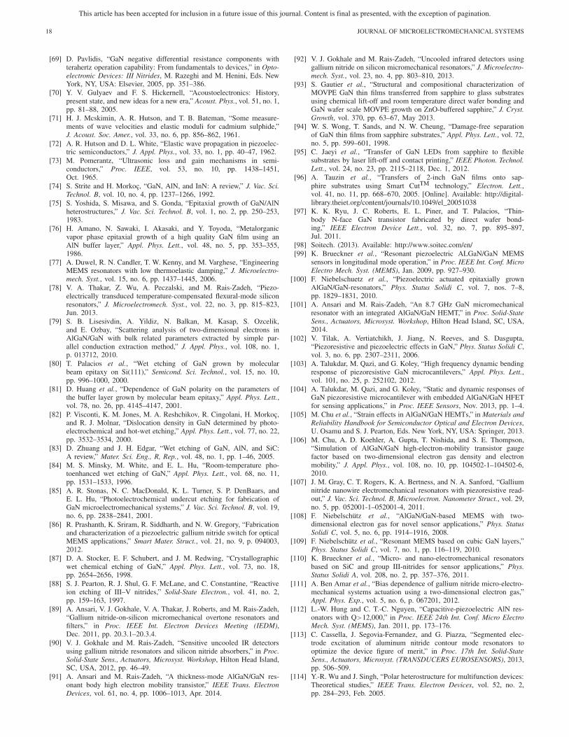
This article has been accepted for inclusion in a future issue of this journal. Content is final as presented, with the exception of pagination.
18 JOURNAL OF MICROELECTROMECHANICAL SYSTEMS
[69] D. Pavlidis, “GaN negative differential resistance components withterahertz operation capability: From fundamentals to devices,” in Opto-electronic Devices: III Nitrides, M. Razeghi and M. Henini, Eds. NewYork, NY, USA: Elsevier, 2005, pp. 351–386.
[70] Y. V. Gulyaev and F. S. Hickernell, “Acoustoelectronics: History,present state, and new ideas for a new era,” Acoust. Phys., vol. 51, no. 1,pp. 81–88, 2005.
[71] H. J. Mcskimin, A. R. Hutson, and T. B. Bateman, “Some measure-ments of wave velocities and elastic moduli for cadmium sulphide,”J. Acoust. Soc. Amer., vol. 33, no. 6, pp. 856–862, 1961.
[72] A. R. Hutson and D. L. White, “Elastic wave propagation in piezoelec-tric semiconductors,” J. Appl. Phys., vol. 33, no. 1, pp. 40–47, 1962.
[73] M. Pomerantz, “Ultrasonic loss and gain mechanisms in semi-conductors,” Proc. IEEE, vol. 53, no. 10, pp. 1438–1451,Oct. 1965.
[74] S. Strite and H. Morkoç, “GaN, AlN, and InN: A review,” J. Vac. Sci.Technol. B, vol. 10, no. 4, pp. 1237–1266, 1992.
[75] S. Yoshida, S. Misawa, and S. Gonda, “Epitaxial growth of GaN/AlNheterostructures,” J. Vac. Sci. Technol. B, vol. 1, no. 2, pp. 250–253,1983.
[76] H. Amano, N. Sawaki, I. Akasaki, and Y. Toyoda, “Metalorganicvapor phase epitaxial growth of a high quality GaN film using anAlN buffer layer,” Appl. Phys. Lett., vol. 48, no. 5, pp. 353–355,1986.
[77] A. Duwel, R. N. Candler, T. W. Kenny, and M. Varghese, “EngineeringMEMS resonators with low thermoelastic damping,” J. Microelectro-mech. Syst., vol. 15, no. 6, pp. 1437–1445, 2006.
[78] V. A. Thakar, Z. Wu, A. Peczalski, and M. Rais-Zadeh, “Piezo-electrically transduced temperature-compensated flexural-mode siliconresonators,” J. Microelectromech. Syst., vol. 22, no. 3, pp. 815–823,Jun. 2013.
[79] S. B. Lisesivdin, A. Yildiz, N. Balkan, M. Kasap, S. Ozcelik,and E. Ozbay, “Scattering analysis of two-dimensional electrons inAlGaN/GaN with bulk related parameters extracted by simple par-allel conduction extraction method,” J. Appl. Phys., vol. 108, no. 1,p. 013712, 2010.
[80] T. Palacios et al., “Wet etching of GaN grown by molecularbeam epitaxy on Si(111),” Semicond. Sci. Technol., vol. 15, no. 10,pp. 996–1000, 2000.
[81] D. Huang et al., “Dependence of GaN polarity on the parameters ofthe buffer layer grown by molecular beam epitaxy,” Appl. Phys. Lett.,vol. 78, no. 26, pp. 4145–4147, 2001.
[82] P. Visconti, K. M. Jones, M. A. Reshchikov, R. Cingolani, H. Morkoç,and R. J. Molnar, “Dislocation density in GaN determined by photo-electrochemical and hot-wet etching,” Appl. Phys. Lett., vol. 77, no. 22,pp. 3532–3534, 2000.
[83] D. Zhuang and J. H. Edgar, “Wet etching of GaN, AlN, and SiC:A review,” Mater. Sci. Eng., R, Rep., vol. 48, no. 1, pp. 1–46, 2005.
[84] M. S. Minsky, M. White, and E. L. Hu, “Room-temperature pho-toenhanced wet etching of GaN,” Appl. Phys. Lett., vol. 68, no. 11,pp. 1531–1533, 1996.
[85] A. R. Stonas, N. C. MacDonald, K. L. Turner, S. P. DenBaars, andE. L. Hu, “Photoelectrochemical undercut etching for fabrication ofGaN microelectromechanical systems,” J. Vac. Sci. Technol. B, vol. 19,no. 6, pp. 2838–2841, 2001.
[86] R. Prashanth, K. Sriram, R. Siddharth, and N. W. Gregory, “Fabricationand characterization of a piezoelectric gallium nitride switch for opticalMEMS applications,” Smart Mater. Struct., vol. 21, no. 9, p. 094003,2012.
[87] D. A. Stocker, E. F. Schubert, and J. M. Redwing, “Crystallographicwet chemical etching of GaN,” Appl. Phys. Lett., vol. 73, no. 18,pp. 2654–2656, 1998.
[88] S. J. Pearton, R. J. Shul, G. F. McLane, and C. Constantine, “Reactiveion etching of III–V nitrides,” Solid-State Electron., vol. 41, no. 2,pp. 159–163, 1997.
[89] A. Ansari, V. J. Gokhale, V. A. Thakar, J. Roberts, and M. Rais-Zadeh,“Gallium nitride-on-silicon micromechanical overtone resonators andfilters,” in Proc. IEEE Int. Electron Devices Meeting (IEDM),Dec. 2011, pp. 20.3.1–20.3.4.
[90] V. J. Gokhale and M. Rais-Zadeh, “Sensitive uncooled IR detectorsusing gallium nitride resonators and silicon nitride absorbers,” in Proc.Solid-State Sens., Actuators, Microsyst. Workshop, Hilton Head Island,SC, USA, 2012, pp. 46–49.
[91] A. Ansari and M. Rais-Zadeh, “A thickness-mode AlGaN/GaN res-onant body high electron mobility transistor,” IEEE Trans. ElectronDevices, vol. 61, no. 4, pp. 1006–1013, Apr. 2014.
[92] V. J. Gokhale and M. Rais-Zadeh, “Uncooled infrared detectors usinggallium nitride on silicon micromechanical resonators,” J. Microelectro-mech. Syst., vol. 23, no. 4, pp. 803–810, 2013.
[93] S. Gautier et al., “Structural and compositional characterization ofMOVPE GaN thin films transferred from sapphire to glass substratesusing chemical lift-off and room temperature direct wafer bonding andGaN wafer scale MOVPE growth on ZnO-buffered sapphire,” J. Cryst.Growth, vol. 370, pp. 63–67, May 2013.
[94] W. S. Wong, T. Sands, and N. W. Cheung, “Damage-free separationof GaN thin films from sapphire substrates,” Appl. Phys. Lett., vol. 72,no. 5, pp. 599–601, 1998.
[95] C. Jaeyi et al., “Transfer of GaN LEDs from sapphire to flexiblesubstrates by laser lift-off and contact printing,” IEEE Photon. Technol.Lett., vol. 24, no. 23, pp. 2115–2118, Dec. 1, 2012.
[96] A. Tauzin et al., “Transfers of 2-inch GaN films onto sap-phire substrates using Smart CutTM technology,” Electron. Lett.,vol. 41, no. 11, pp. 668–670, 2005. [Online]. Available: http://digital-library.theiet.org/content/journals/10.1049/el_20051038
[97] K. K. Ryu, J. C. Roberts, E. L. Piner, and T. Palacios, “Thin-body N-face GaN transistor fabricated by direct wafer bond-ing,” IEEE Electron Device Lett., vol. 32, no. 7, pp. 895–897,Jul. 2011.
[98] Soitech. (2013). Available: http://www.soitec.com/en/[99] K. Brueckner et al., “Resonant piezoelectric ALGaN/GaN MEMS
sensors in longitudinal mode operation,” in Proc. IEEE Int. Conf. MicroElectro Mech. Syst. (MEMS), Jan. 2009, pp. 927–930.
[100] F. Niebelschuetz et al., “Piezoelectric actuated epitaxially grownAlGaN/GaN-resonators,” Phys. Status Solidi C, vol. 7, nos. 7–8,pp. 1829–1831, 2010.
[101] A. Ansari and M. Rais-Zadeh, “An 8.7 GHz GaN micromechanicalresonator with an integrated AlGaN/GaN HEMT,” in Proc. Solid-StateSens., Actuators, Microsyst. Workshop, Hilton Head Island, SC, USA,2014.
[102] V. Tilak, A. Vertiatchikh, J. Jiang, N. Reeves, and S. Dasgupta,“Piezoresistive and piezoelectric effects in GaN,” Phys. Status Solidi C,vol. 3, no. 6, pp. 2307–2311, 2006.
[103] A. Talukdar, M. Qazi, and G. Koley, “High frequency dynamic bendingresponse of piezoresistive GaN microcantilevers,” Appl. Phys. Lett.,vol. 101, no. 25, p. 252102, 2012.
[104] A. Talukdar, M. Qazi, and G. Koley, “Static and dynamic responses ofGaN piezoresistive microcantilever with embedded AlGaN/GaN HFETfor sensing applications,” in Proc. IEEE Sensors, Nov. 2013, pp. 1–4.
[105] M. Chu et al., “Strain effects in AlGaN/GaN HEMTs,” in Materials andReliability Handbook for Semiconductor Optical and Electron Devices,U. Osamu and S. J. Pearton, Eds. New York, NY, USA: Springer, 2013.
[106] M. Chu, A. D. Koehler, A. Gupta, T. Nishida, and S. E. Thompson,“Simulation of AlGaN/GaN high-electron-mobility transistor gaugefactor based on two-dimensional electron gas density and electronmobility,” J. Appl. Phys., vol. 108, no. 10, pp. 104502-1–104502-6,2010.
[107] J. M. Gray, C. T. Rogers, K. A. Bertness, and N. A. Sanford, “Galliumnitride nanowire electromechanical resonators with piezoresistive read-out,” J. Vac. Sci. Technol. B, Microelectron. Nanometer Struct., vol. 29,no. 5, pp. 052001-1–052001-4, 2011.
[108] F. Niebelschütz et al., “AlGaN/GaN-based MEMS with two-dimensional electron gas for novel sensor applications,” Phys. StatusSolidi C, vol. 5, no. 6, pp. 1914–1916, 2008.
[109] F. Niebelschütz et al., “Resonant MEMS based on cubic GaN layers,”Phys. Status Solidi C, vol. 7, no. 1, pp. 116–119, 2010.
[110] K. Brueckner et al., “Micro- and nano-electromechanical resonatorsbased on SiC and group III-nitrides for sensor applications,” Phys.Status Solidi A, vol. 208, no. 2, pp. 357–376, 2011.
[111] A. Ben Amar et al., “Bias dependence of gallium nitride micro-electro-mechanical systems actuation using a two-dimensional electron gas,”Appl. Phys. Exp., vol. 5, no. 6, p. 067201, 2012.
[112] L.-W. Hung and C. T.-C. Nguyen, “Capacitive-piezoelectric AlN res-onators with Q>12,000,” in Proc. IEEE 24th Int. Conf. Micro ElectroMech. Syst. (MEMS), Jan. 2011, pp. 173–176.
[113] C. Cassella, J. Segovia-Fernandez, and G. Piazza, “Segmented elec-trode excitation of aluminum nitride contour mode resonators tooptimize the device figure of merit,” in Proc. 17th Int. Solid-StateSens., Actuators, Microsyst. (TRANSDUCERS EUROSENSORS), 2013,pp. 506–509.
[114] Y.-R. Wu and J. Singh, “Polar heterostructure for multifunction devices:Theoretical studies,” IEEE Trans. Electron Devices, vol. 52, no. 2,pp. 284–293, Feb. 2005.

This article has been accepted for inclusion in a future issue of this journal. Content is final as presented, with the exception of pagination.
RAIS-ZADEH et al.: GaN AS AN ELECTROMECHANICAL MATERIAL 19
[115] M. Faucher et al., “Amplified piezoelectric transduction of nanoscalemotion in gallium nitride electromechanical resonators,” Appl. Phys.Lett., vol. 94, no. 23, pp. 233506-1–233506-3, 2009.
[116] S.-H. Lee, H.-H. Jeong, S.-B. Bae, H.-C. Choi, J.-H. Lee, andY.-H. Lee, “Epitaxially grown GaN thin-film SAW filter with highvelocity and low insertion loss,” IEEE Trans. Electron Devices, vol. 48,no. 3, pp. 524–529, Mar. 2001.
[117] T. Palacios et al., “High frequency SAW devices on AlGaN: Fabri-cation, characterization and integration with optoelectronics,” in Proc.IEEE Ultrason. Symp., Oct. 2002, pp. 57–60.
[118] A. Müller et al., “SAW devices manufactured on GaN/Si for frequen-cies beyond 5 GHz,” IEEE Electron Device Lett., vol. 31, no. 12,pp. 1398–1400, Dec. 2010.
[119] K.-Y. Wong, W. Tang, K. M. Lau, and K. J. Chen, “Planartwo-dimensional electron gas (2DEG) IDT SAW filter on AlGaN/GaNheterostructure,” in Proc. IEEE/MTT-S Int. Microw. Symp. (IMS),Jun. 2007, pp. 2043–2046.
[120] L. Shao, M. Zhang, A. Banerjee, P. Bhattacharya, and K. P. Pipe,“Emission and detection of surface acoustic waves by AlGaN/GaNhigh electron mobility transistors,” Appl. Phys. Lett., vol. 99, no. 24,p. 243507, 2011.
[121] M. Faucher, G. Martin, J.-M. Friedt, and S. Ballandras, “A 1 GHzSAW oscillator on epitaxial GaN/Si substrate: Toward co-integratedfrequency sources,” in Proc. Joint Eur. Freq. Time Forum Int. Freq.Control Symp. (EFTF/IFCS), Jul. 2013, pp. 21–24.
[122] V. B. Braginsky and V. P. Mitrofanov, Systems With Small Dissi-pation, K. S. Thorne, Ed. Chicago, IL, USA: Univ. Chicago Press,pp. 1–42, 1985.
[123] V. T. Srikar and S. D. Senturia, “Thermoelastic damping in fine-grained polysilicon flexural beam resonators,” J. Microelectromech.Syst., vol. 11, no. 5, pp. 499–504, Oct. 2002.
[124] S. A. Chandorkar, M. Agarwal, R. Melamud, R. N. Candler,K. E. Goodson, and T. W. Kenny, “Limits of quality factor in bulk-mode micromechanical resonators,” in Proc. IEEE 21st Int. Conf. MicroElectro Mech. Syst. (MEMS), Jan. 2008, pp. 74–77.
[125] A. Müller et al., “6.3-GHz film bulk acoustic resonator structures basedon a gallium nitride/silicon thin membrane,” IEEE Electron DeviceLett., vol. 30, no. 8, pp. 799–801, Aug. 2009.
[126] J. Kaitila, “BAW device basics,” in RF Bulk Acoustic Wave Filtersfor Communications, K.-Y. Hashimoto, Ed. Norwood, MA, USA:Artech House, 2009, pp. 51–90.
[127] R. Wang, S. A. Bhave, and K. Bhattacharjee, “High k2t × Q, multi-
frequency lithium niobate resonators,” in Proc. IEEE Int. Conf. MicroElectro Mech. Syst. (MEMS), Jan. 2013, pp. 165–168.
[128] R. Ruby, P. Bradley, J. Larson, III, Y. Oshmyansky, and D. Figueredo,“Ultra-miniature high-Q filters and duplexers using FBAR technology,”in Proc. IEEE Int. Solid-State Circuits Conf. (ISSCC), Feb. 2001,pp. 120–121.
[129] C. Durand et al., “In-plane silicon-on-nothing nanometer-scale res-onant suspended gate MOSFET for in-IC integration perspec-tives,” IEEE Electron Device Lett., vol. 29, no. 5, pp. 494–496,May 2008.
[130] D. Grogg, M. Mazza, D. Tsamados, and A. M. Ionescu, “Multi-gatevibrating-body field effect transistor (VB-FETs),” in Proc. IEEE Int.Electron Devices Meeting (IEDM), Dec. 2008, pp. 1–4.
[131] D. Weinstein and S. A. Bhave, “The resonant body transistor,” NanoLett., vol. 10, no. 4, pp. 1234–1237, 2010.
[132] M. Faucher, Y. Cordier, M. Werquin, L. Buchaillot, C. Gaquiere,and D. Theron, “Electromechanical transconductance properties ofa GaN MEMS resonator with fully integrated HEMT transduc-ers,” J. Microelectromech. Syst., vol. 21, no. 2, pp. 370–378,Apr. 2012.
[133] R. Ram Yadav and D. K. Pandey, “Ultrasonic characterisation ofgallium nitride,” Mater. Res. Innov., vol. 10, no. 4, pp. 402–407, 2006.
[134] A. Ansari and M. Rais-Zadeh, “A temperature-compensated micro-mechanical gallium nitride resonator,” IEEE Electron Device Lett.,to be published.
[135] C. D. Nordquist and R. H. Olsson, “Power handling and intermodu-lation distortion of contour-mode AlN MEMS resonators and filters,”in Proc. IEEE/MTT-S Int. Microw. Symp. (IMS), Jun. 2011, pp. 1–4.
[136] M. Razeghi, “Short-wavelength solar-blind detectors-status, prospects,and markets,” Proc. IEEE, vol. 90, no. 6, pp. 1006–1014,Jun. 2002.
Mina Rais-Zadeh (S’03–M’08–SM’12) receivedthe B.S. degree in electrical engineering from theSharif University of Technology, Tehran, Iran, in2002, and the M.S. and Ph.D. degrees in electricaland computer engineering from the Georgia Instituteof Technology, Atlanta, GA, USA, in 2005 and 2008,respectively. From 2008 to 2009, she was a Post-Doctoral Research Fellow with the Georgia Instituteof Technology. Since 2009, she has been with theUniversity of Michigan, Ann Arbor, MI, USA, whereshe is currently an Associate Professor of Electrical
Engineering and Computer Science.She was a recipient of the NSF CAREER Award (2011), the IEEE Electron
Device Society’s Early Career Award (2011), the NASA Early Career FacultyAward (2012), the Crosby Research Award from the University of Michigan(2013), and the ONR Young Investigator Award (2014). She was one of the 81invitees by the National Academy of Engineering to attend the 19th AnnualFrontiers of Engineering Symposium (2013). Together with her students, shereceived several best paper awards at the Transducers Conference, the IEEESiRF conferences, and the International Microwave Symposiums. She is amember of the 2014 IEDM Executive Committee and the 2015 IEEE MEMSExecutive Committee, and has served as a Technical Program CommitteeMember of the IEEE International Electron Devices Meeting (2011–2013),the IEEE Sensors Conference (2011–2014), the Hilton Head Workshop (2012,2014), the IEEE MEMS Conference (2014–2015), the Transducers Conference(2015), and the International Frequency Control Symposium (2015). She isan Associate Editor of the IEEE ELECTRON DEVICE LETTERS. Her researchinterests include electron devices for wireless communication and sensingapplications and the related device physics, resonant micromechanical devices,RF microelectromechanical systems (MEMS), gallium nitride MEMS, andmicro/nano fabrication process development.
Vikrant Jayant Gokhale (S’10) received theB.Tech. degree in electronics and instrumentationengineering from the Vellore Institute of Technology,Vellore, India, in 2007, and the M.S. and Ph.D.degrees in electrical and computer engineering fromthe University of Michigan, Ann Arbor, MI, USA,in 2010 and 2014, respectively.
He was an Engineer with Honeywell TechnologySolutions, Sensing, and Control, Bangalore, India,from 2007 to 2008. Since 2014, he has been a Post-Doctoral Researcher with the Physical Measurement
Laboratory, National Institute of Standards and Technology, Gaithersburg,MD, USA. His specific research interests include high-frequency micro-electromechanical systems (MEMS) resonators and associated energy lossmechanisms, and resonant MEMS sensors for detecting physical phenomena,such as infrared radiation.
Azadeh Ansari (S’10) received the B.S. degreein electrical engineering from the Sharif Universityof Technology, Tehran, Iran, in 2010. She joinedthe University of Michigan, Ann Arbor, MI, USA,in 2011, where she received the M.S. degree in2013 and is currently pursuing the Ph.D. degree.Her research interests include GaN-based microme-chanical resonators, integration of GaN HEMTs andmicroelectromechanical systems (MEMS), resonanttransistors, and interface circuit design for MEMS.

This article has been accepted for inclusion in a future issue of this journal. Content is final as presented, with the exception of pagination.
20 JOURNAL OF MICROELECTROMECHANICAL SYSTEMS
Marc Faucher received the M.S. degree in physicsfrom the University of Marseille, Marseille, France,in 2002; the Engineer’s degree from École Centralede Marseille, Marseille; and the Ph.D. degree inphysics from Joseph Fourier University, Grenoble,France, in 2003, where he studied superconductingnanocircuits.
He was a Post-Doctoral Researcher with theAtomic Energy Commission-Laboratory for Elec-tronics and Information Technology, Grenoble, from2003 to 2005, where he was worked on semicon-
ductor characterization techniques. He joined the Institute of Electronics,Microelectronics, and Nanotechnology (IEMN), Lille, France (CNRS UMR8520), in 2006, as a Post-Doctoral Researcher.
Dr. Faucher is currently a Centre National de la Recherche ScientifiqueResearcher with the Nano and Microsystems Group, IEMN. His research isrelated to microelectromechanical systems (MEMS) and nanoelectromechan-ical systems, including silicon resonators for high-frequency sensing systems,micro/nanofabrication, and the design, fabrication, and characterization ofgallium nitride MEMS/high-electron mobility transistors.
Didier Théron was born in Auxerre, France, in1962. He received the Dipl.-Ing. degree from ÉcolePolytechnique, Palaiseau, France, in 1984; the Mas-ter’s degree in solid-state physics from the Univer-sity of Paris-Sud, Orsay, France, in 1985; and thePh.D. degree in physics from the Swiss FederalInstitute of Technology, Lausanne, Switzerland, in1989, with a focus on the physical simulation andMBE growth of GaAs-based multichannel HEMTs.Since 1990, he has been with the Centre Nationalde la Recherche Scientifique (CNRS), Paris, where
he is currently the Research Director. He is performing his research activitywith the Institute of Electronics, Microelectronics, and Nanotechnology,Villeneuve d’Ascq, France, where he worked on the physics and technologyof GaAs and InP-based power HEMTs for millimeter-wave applications(from 10 to 94 GHz). He worked on GaN HEMTs in cooperation with theAlcatel/Thales III-V Laboratory, Palaiseau. Since 2006, he has worked onGaN microelectromechanical systems (MEMS) resonator physics. He is alsoinvolved in Si MEMS resonator device physics for atomic force detection andRF electrical property characterization of dielectric materials using scanningmicrowave microscopy developed in cooperation with Agilent Technologies,Santa Clara, CA, USA.
He has been successively involved in research administration as a ScientificAdvisor of Microelectronics with CNRS, the Program Director of Nanotech-nology and Nanosystems with the National Research Agency, and morerecently, an Advisor of Nanotechnology with the French Ministry of Research,since 2004. He has authored about 120 publications and communications, andwas a recipient of the Bronze Medal from CNRS in 1998.
Yvon Cordier was born in France in 1965. Hereceived the degree in materials science engineeringfrom the EUDIL School of Engineering, Univer-sity of Lille, Villeneuve-d’Ascq, France, in 1988,and the Ph.D. degree from the Lille Universityof Science and Technology, Villeneuve-d’Ascq, in1992. In 1991, he joined the Central ResearchLaboratory of Thomson-CSF, Orsay, France, wherehe developed III–V epitaxial structures for elec-tronic and optoelectronic devices. In 1996, he joinedthe Institute of Electronics, Microelectronics, and
Nanotechnology, Villeneuve d’Ascq, France, as a Centre National de laRecherche Scientifique (CNRS) permanent Researcher, and studied the growthof AlInAs/GaInAs metamorphic heterostructures on GaAs substrate. In 2001,he joined the Centre de Recherche sur l’HétéroEpitaxie et ses Applications-CNRS, Valbonne, France. He has authored or co-authored over 180 publica-tions, holds two patents, and is heading, as the Research Director, a teamworking on the growth of semiconductor materials, including GaN, SiC,Graphene, and ZnO, for electronics.
Lionel Buchaillot is currently a Centre Nationalde la Recherche Scientifique (CNRS) SeniorResearcher. He received the M.S. degree in mate-rial sciences and the Ph.D. degree in mechanicalengineering from the Université de Franche-Comté,Besançon, France, in 1991 and 1995, respectively.From 1995 to 1997, he was with the Laboratoryfor Integrated MicroMechatronic Systems-CNRS-IIS, University of Tokyo, Tokyo, Japan, as a JSPSPost-Doctoral Fellow working on thin-film shapememory alloys actuators for microelectromechanical
systems (MEMS). In 1997, he was a Research and Development Engineer withSAFRAN, Paris, France, and AVIAC Technologies, Mantes-la-Jolie, France.In 1998, he joined the Department of ISEN, CNRS, Institute of Electronics,Microelectronics and Nanotechnology (IEMN), Villeneuve d’Ascq, France. Hewas the Head of the Silicon-Based MEMS Research Group at IEMN from2001 to 2009. In 2010, he became the Director of IEMN. His research focuseson mechanical sensors and systems, RF MEMS/MEMS for microwaves,and scientific micro and nanoinstruments. He has authored or co-authoredover 100 papers and several book chapters. He is an Editor of the IEEEJOURNAL OF MICROELECTROMECHANICAL SYSTEMS and the IOP’s Journalof Micromechanics and Microengineering. He was a recipient of the CNRSBronze Medal.