joining of silver nanowires - uwspace home
TRANSCRIPT

Metallurgical Issues in Low-Temperature
Joining of Silver Nanowires
by
Peng Peng
A thesis
presented to the University of Waterloo
in fulfillment of the
thesis requirement for the degree of
Doctor of Philosophy
in
Mechanical Engineering - Nanotechnology
Waterloo, Ontario, Canada, 2014
©Peng Peng 2014

ii
AUTHOR'S DECLARATION
I hereby declare that I am the sole author of this thesis. This is a true copy of the thesis, including any
required final revisions, as accepted by my examiners.
I understand that my thesis may be made electronically available to the public.

iii
Abstract
Silver nanowires (Ag NWs) have a wide range of applications in the electronic industry and
are attracting growing world-wide interest because of their unique thermal, chemical, electrical and
mechanical properties. Understanding of mechanical properties of Ag NWs and joining processes for
them at a nano scale is urgently needed to support exploitation of their applications. Particularly,
study of processing-structure-property relationships is of much significance. In the present thesis, the
following research works were conducted.
Ag NWs were synthesized using the polyol method. Joining of individual Ag NWs in an end-
to-end orientation at room-temperature without assistance of external pressure was investigated.
Selective surface activation of Ag NWs provided surface free of protective organic layers for
metallurgical joining. A similar crystal orientation was maintained between the NWs, and diffusion
along the boundary contributed to the nanojunction formation. Monocrystalline V-shaped or zig-zag
silver prisms were formed after nanojoining, terminated by twin boundaries and free surfaces.
The feasibility of room-temperature pressure-free joining of copper (Cu) substrates using Ag
NW paste was conducted and demonstrated for flexible electronic packaging applications. The
organic content in water-based Ag NW pastes was largely reduced by a repeated washing process to
decrease the joining temperature. The formation of end-to-side or side-to-side joints between Ag
NWs was observed concurrently with those joined end-to-end. The mechanical and electrical
properties of Ag NW joints were examined. It was found that self-generated local heating within the
Ag NW paste and Cu substrate system promoted the joining of Ag-to-Ag and Ag-to-Cu without any
external energy input. The localized heat energy could be delivered in-situ to the interfaces and
promoted atomic diffusion and metallic bond formation while the bulk component temperature
maintaining near room-temperature. The organic layer on the side surfaces of the Ag NWs could be
broken down through consumption of the residual PVP by a CuO-PVP reaction and which produced
localized heating, increasing activated surface sites dramatically and making three-dimensional
networks feasible.
Ag NWs were introduced into Ag nanoparticle (NP) matrices joined at low-temperature.
Joining was facilitated by solid state sintering of the Ag nanomaterials and metallic bonding at Cu-Ag
interfaces. It was found that Ag NWs in a Ag NP matrix acted as a second reinforcement phase. In

iv
addition to improving the fracture toughness of joints, the introduction of Ag NWs affected the path
of fracture propagation, where necking, breakage and pullout of Ag NWs occurred during loading.

v
Acknowledgements
At the end of my enjoyable and difficult journey in obtaining a Ph.D. degree, I would like to
thank all those people who contributed in many ways to the success of this project and made it an
unforgettable experience for me.
The greatest gratitude should go to my supervisors, Dr. Y. Norman Zhou, and Dr. Adrian P
Gerlich. I am sincerely indebted to them from their incredible knowledge and deep insight in the field
of joining and materials science. They introduced me into this interesting research area with their
ongoing and unconditional guidance during my study at the University of Waterloo. They have taught
me, both consciously and un-consciously, to have a sharp mind and eyes in science while keeping a
good, well-rounded attitude. Without their continual guidance, encouragement and support, this work
would not have been possible.
I wish to express my sincere appreciation to Dr. Anming Hu at the University of Tennessee.
Dr. Hu set up a good example for me when he was at CAMJ. He is smart, hard-working and stringent
with scientific research. Three years of working with him is successful and important for my future
career. I would also like to thank Dr. Xiaogang Li, Dr. Yuquan Ding, Dr. Lei Liu and Dr. Scott
Lawson at the University of Waterloo for their thoughtful discussion and suggestions of research and
technical writings.
I would also like to thank all my friends inside and outside the CAMJ group for all their
assistance: Yongde Huang, Andie Pequegnat, Golnaz Bohlouli, Robert Liang, Matthew Daly, Hong
Huang, Ehsan Marzban, Wenchao Ma, and other good friends. Very special thanks to Chao Jin in
Civil Engineering for discussion and exchanging critical thoughts on state-of-the-art technologies and
interesting papers for learning new things and inspiring new ideas.
I greatly appreciate the financial support of the State Scholarship Fund of China during my
study. Finally, a special thought is also devoted to my parents and my sister for the never-ending
support. Their understanding and their endless love encouraged me to work hard and to continue
pursuing a Ph.D. degree abroad.

vi
Dedication
To My Family

vii
Table of Contents
AUTHOR'S DECLARATION ............................................................................................................... ii
Abstract ................................................................................................................................................. iii
Acknowledgements ................................................................................................................................ v
Dedication ............................................................................................................................................. vi
Table of Contents ................................................................................................................................. vii
List of Figures ........................................................................................................................................ x
List of Tables ....................................................................................................................................... xix
Chapter 1 Introduction ............................................................................................................................ 1
1.1 Low Temperature Joining Process ............................................................................................... 2
1.2 Mechanical Properties of Porous Materials .................................................................................. 4
1.3 Motivation of Research ................................................................................................................ 5
1.3.1 Issues Associated with Flexible Electronic Packaging .......................................................... 6
1.3.2 Advantages of Low-Temperature Joining of Ag NW Pastes ................................................ 6
1.3.3 Mechanical Properties of Ag Nanoporous Materials ............................................................. 7
1.4 Objectives and Contributions of Research ................................................................................... 7
1.5 Dissertation Organization ............................................................................................................. 9
Chapter 2 Literature Review ................................................................................................................ 10
2.1 Overview of Ag Nanomaterials .................................................................................................. 10
2.1.1 Synthesis of Ag Nanomaterials ........................................................................................... 11
2.1.2 Mechanical Properties of Ag Nanomaterials ....................................................................... 14
2.1.3 Nano-indentation Characterization ...................................................................................... 27
2.2 Joining of Ag Nanomaterials ...................................................................................................... 35
2.2.1 Basic Joining Concepts ........................................................................................................ 36
2.2.2 Size Effects on Low Temperature Sintering ........................................................................ 37
2.2.3 Progress in Low Temperature Joining of Ag Nanomaterials .............................................. 39
2.2.4 Joining of Ag NWs .............................................................................................................. 45
2.3 Problem Summary ...................................................................................................................... 48
Chapter 3 Joining of Individual Silver Nanowires ............................................................................... 49
3.1 Introduction ................................................................................................................................ 49
3.2 Experimental............................................................................................................................... 50
3.2.1 Synthesis of Ag NWs .......................................................................................................... 50

viii
3.2.2 Surface Activation Process .................................................................................................. 50
3.2.3 Characterization of Ag NWs ............................................................................................... 50
3.3 Results ........................................................................................................................................ 51
3.3.1 Comparison of As-synthesized and Washed Ag NWs ........................................................ 51
3.3.2 Effects of Ultrasonication and Centrifugation ..................................................................... 52
3.3.3 Joint Selection ..................................................................................................................... 54
3.3.4 Angle Measurement and Distribution .................................................................................. 54
3.4 Discussion .................................................................................................................................. 57
3.4.1 Selective Surface Activation ............................................................................................... 57
3.4.2 Phase Relationships of Joints .............................................................................................. 60
3.4.3 Joining Mechanism: Self-Oriented Nanojoining ................................................................. 64
3.5 Summary and Remarks ............................................................................................................... 66
Chapter 4 Joining Using Silver Nanowire Pastes ................................................................................. 68
4.1 Introduction ................................................................................................................................ 68
4.2 Experimental............................................................................................................................... 69
4.2.1 Synthesis of Ag NW pastes ................................................................................................. 69
4.2.2 Thermogravimetric Analysis ............................................................................................... 69
4.2.3 Joining using Ag NW Pastes ............................................................................................... 70
4.2.4 Tensile Testing .................................................................................................................... 70
4.2.5 Nanoindentation .................................................................................................................. 71
4.2.6 Resistivity Measurement ..................................................................................................... 71
4.2.7 Microstructural Characterization ......................................................................................... 71
4.2.8 Local Heat Measurement ..................................................................................................... 72
4.3 Results ........................................................................................................................................ 72
4.3.1 Organic Content in the Pastes .............................................................................................. 72
4.3.2 Sintering Behaviors and Weldability of Pastes ................................................................... 75
4.3.3 Mechanical Properties of Ag NW Joints ............................................................................. 76
4.3.4 Mechanical Properties of Ag NW Porous Materials ........................................................... 79
4.3.5 Electrical Property of Ag NW Joints ................................................................................... 80
4.3.6 Microstructure Characterization .......................................................................................... 82
4.4 Discussion .................................................................................................................................. 85
4.4.1 Self-generated Local Heat ................................................................................................... 85

ix
4.4.2 Local Heat: Lumped Capacity Model ................................................................................. 87
4.4.3 Interfacial Reaction ............................................................................................................. 89
4.4.4 Local Temperature ............................................................................................................... 91
4.4.5 Local Heating Effects Induced Nanojoining ....................................................................... 95
4.5 Summary and Remarks ............................................................................................................... 97
Chapter 5 Reinforcement of Silver Nanoparticle Joints with Nanowires ............................................. 99
5.1 Introduction ................................................................................................................................ 99
5.2 Experimental............................................................................................................................. 100
5.2.1 Synthesis of Ag NPs and NWs .......................................................................................... 100
5.2.2 Joining using Ag NP-NW Binary Pastes ........................................................................... 101
5.2.3 Tensile Testing .................................................................................................................. 101
5.2.4 Nanoindentation ................................................................................................................ 102
5.2.5 Microstructure Characterization ........................................................................................ 102
5.3 Results ...................................................................................................................................... 102
5.3.1 Microstructures of Sintered Ag NPs and Ag NWs ............................................................ 102
5.3.2 Mechanical Properties ....................................................................................................... 106
5.3.3 Fracture Behaviours of Joints ............................................................................................ 110
5.4 Discussion ................................................................................................................................ 114
5.4.1 Fracture Energy ................................................................................................................. 114
5.4.2 Reinforcement Mechanisms .............................................................................................. 115
5.5 Summary and Remarks ............................................................................................................. 118
Chapter 6 Conclusions and Recommendations for Future Work ....................................................... 120
6.1 Conclusions .............................................................................................................................. 120
6.2 Recommendations for Future Work ......................................................................................... 122
Reference ............................................................................................................................................ 124

x
List of Figures
Figure 1.1 (a) Schematic of bonding with sintered nanomaterial fillers, T, P and t stand for sintering
temperature, pressure and time, respectively. Interface qualities of nanomaterials - nanomaterials (b)
and nanomaterials - substrates (c) affecting the joint properties (the critical separation distances of
particle interfaces, x, and particle centres, y). ......................................................................................... 4
Figure 2.1 Typical micrographs of Ag NPs prepared with seed-mediated method with (a-b) different
precursor volumes and (c-d) different seed solution volumes; Arrow in (d) indicating the multiply
twined structure. (reproduced from 57
) ................................................................................................. 11
Figure 2.2 (a) SEM image of Ag NWs with pentagonal cross section. Schematic illustration of the
mechanism proposed to account for the growth of silver nanowires with pentagonal cross sections: (b)
Evolution of a nanorod from a MTP terminated by 111 end facets, and 100 side facets. (c)
Diffusion of silver atoms toward the two ends of a nanorod, with the side surfaces completely
passivated by PVP. (reproduced from 66
) ............................................................................................. 13
Figure 2.3 (a) HRTEM image of the cross-section of the Ag nanowires; the scale bar is 2 nm. The
2.08Å spacing labeled by white lines is indexed as d002. The inset shows the model of the 7.5° misfit
angle of a five twinned crystal. (b) Schematic illustration of the truncated decahedronal structure of
Ag NW bounded by five [100] planes and capped by ten [111] planes at both the tips of the Ag NW,
whose growth direction is along [110]. (c) The cross-section of the Ag NW, two distinct layers of five
[110] plane subunits, overlapped onto each other. (reproduced from 70
) ............................................. 14
Figure 2.4 (a) Hall-Petc
h and inverse Hall-Petch behavior in nanocrystalline copper; ∆H is the increment of hardness and d is
grain size. (b) Schematic diagram of strength of polycrystalline materials as a function of grain size
with Hall-Petch and inverse Hall-Petch relations involving the deformation mechanisms. (reproduced
from 73, 76, 86
) .......................................................................................................................................... 16
Figure 2.5 Sample size dependence of yield strength in micro/nano pillars under compression
punched with flat indenter. The surface effect and strain rate will affect the deformation process.
(experimental data from 94
, image from 95, 96
) ....................................................................................... 17
Figure 2.6 Tensile testing of polycrystalline silver microwires with different grain sizes (d) and
sample diameters (t). (a) Hall-Petch relationship applied to the 0.2% yielding strength. Analysis of the

xi
proof strength with the relation of (b) sample size (t) and (c) shape effects (t/d) and (d) cooperated
effects of sample and shape. (reproduced from 97
) ............................................................................... 18
Figure 2.7 (a) In-situ TEM tensile test of penta-twinned Ag NWs with a diameter of 42 nm. (b)
Experimental stress-strain curves of Ag NWs of varying diameter. The roman numerals I-IV on the
stress-strain curve indicating the recording times of the corresponding TEM images in (a).
(reproduced from 99
) ............................................................................................................................. 20
Figure 2.8 Images before and after deformation of (a) region where fracture occurred and (b) plastic
region away from fracture point. Surface nucleation of stacking fault decahedra (SFD) formation in
thin Ag NWs: Simulation snapshot of (c) the first partial dislocation nucleation from a penta-twinned
Ag NW with D = 12 nm; (d) front side of the stacking fault decahedron (SFD) formed following the
first dislocation nucleation event in (c); (e) A sequence of SFDs formed along the NW axis following
the first SFD in (d). (f) TEM image of plastic region in NW, the inset shows a SAED pattern recorded
from the same NW region indicating the [110] growth direction (d220 = 0.148). (reproduced from 99
)21
Figure 2.9 Elastic modulus data from molecular statics simulations of ⟨110⟩ axially oriented
nanowires with square, rhombic, and pentagonal cross-sectional geometry. “Nanowire thickness” is
the shortest lateral dimension of each cross section. (reproduced from 101
) ......................................... 22
Figure 2.10 (a) Size effect on the tensile yield strength of pentagonal, rhombic, and truncated-rhombic
silver nanowires; Snapshots of silver nanowires with (b) pentagonal cross-section of 2.56 nm, (c)
truncated rhombic cross-section of 1.9 nm, and (d) rhombic cross-section of 2.2 nm during tensile
deformation at 300 K. (reproduced from 102
) ........................................................................................ 23
Figure 2.11 AFM images of pentagonal silver nanowire with 23.6 nm in diameter (a) before bending
and (b) after failure. (Scale bars are 250 nm). (c) F-d curves recorded during the consecutive
manipulation by AFM tip-induced lateral bending of a 23.6 nm pentagonal silver nanowire. Curves 1
and 2 show that the wire was elastically loaded and unloaded. The unloading points are identified as
vertical dashed lines. Curve 3 is a single shot experiment and shows nonlinear elastic behavior of
silver nanowire, followed by limited plastic deformation and then brittle failure. Note that F-d curves
are shifted for clarity. Inset: schematic of bending test showing that the bending angle defined as the
angle between the deformed wire and its original direction. (reproduced from 103
) ............................. 25
Figure 2.12. A schematic diagram of load-displacement curve from an indentation experiment. The
quantities shown are Pmax: the peak indentation load; hmax: the indenter displacement at the peak load;

xii
hf: the final depth of the contact impression after unloading; and S: the initial unloading stiffness.
(reproduced from 110
) ............................................................................................................................ 29
Figure 2.13 TEM image taken from the in situ nanoindentation experiment. (a) the probe and silver
nanoparticle before the nanoindentation. (b-e) during indentation, where contrast bands highlighted
with A-H. (f) the probe and nanoparticle after deformation. (reproduced from 114
) ............................ 31
Figure 2.14 HRTEM image of (a) silver nanoparticle before compression, the present twin is
highlighted; the (b) beginning and (c) middle of indentation, an edge dislocation is highlighted in the
inset; (d) after indenter is removed. (reproduced from 114
)................................................................... 31
Figure 2.15 a EM image of solution-derived nanoparticle silver ink thin films sintered at 150 C for
5-min. (b) Nanoindentation load-displacement curve for nanoink silver film on a Si substrate. (c)
Indentation hardness as a function of fractional indentation depth. (reproduce from 115
) .................... 33
Figure 2.16 (a,b) AFM images of indents on silver nanowires after nanoindentation; (c) height profile
of an indent on the wire and (d) a representative nanoindentation load-displacement curve.
(reproduced from 111
) ............................................................................................................................ 35
Figure 2.17 MD simulation of two large particles sintering at T = 63% Tm. (a-d) without grain
boundary and (e-h) with grain boundary. Snapshots for the sintering process are t = 500, 50000,
200000 and 500000 steps. Every particle contains around 3000 atoms with bulk atoms (blue), surface
or grain boundary atoms (red) and vapour state atoms (cyan), respectively. (reproduced from 157
) .... 38
Figure 2.18 Strength of joints bonded at different temperatures. (data from 18, 172, 174, 177
) ................... 41
Figure 2.19 Strength of joints bonded with Ag nanomaterials at different sintering times. (data from
16, 174, 175, 178-182) ...................................................................................................................................... 42
Figure 2.20 Strength of joints bonded at different external pressures. (data from 164, 173, 175, 183, 184
) ..... 43
Figure 2.21 Particle size effect on the strength of sintered nanomaterial joins. Closed symbols indicate
that the sizes are uniform in the pastes; Open symbols represent average sizes of nanoparticles in the
pastes with different gradations and the size distribution is represented as a solid line covering a range.
(data from 173, 185
) .................................................................................................................................. 44
Figure 2.22 (a) Schematic illustration of chemically activated joining using cationic polymer or
electrolyte solution. The microstructure of Ag NPs before (b) and after (c) applying cationic polymer.
(reproduced from 186-189
) ....................................................................................................................... 45

xiii
Figure 2.23 Optical nanowelding set-up and scanning electron microscope (SEM) images before and
after illumination. Finite element method simulations of optical heat generation at silver nanowire
junctions during the nanowelding process. (reproduced from 9) .......................................................... 47
Figure 2.24 Ag NW film: before (a) and after (b) applying 25 MPa pressure for 5 seconds.
(reproduced from 201
) ............................................................................................................................ 48
Figure 3.1 Optical and SEM micrographs of (a,c) as-synthesized and (b,d) washed Ag NWs, illustrate
that the V-shaped and zig-zag Ag NWs significantly increased after washing. ................................... 51
Figure 3.2 SEM images of (a) pristine Ag NWs in EG and after washing with (b) water, (c) acetone
and (d) ethanol. ..................................................................................................................................... 52
Figure 3.3 Optical images of Ag NWs after ultrasoncating with different time and energy. (a-d scale
bars are 20 μm ..................................................................................................................................... 53
Figure 3.4 SEM images of V-shaped NWs formed (a) between two thin or thick NWs; (b) Thick NWs
to thin NW. ........................................................................................................................................... 53
Figure 3.5 Difference of (a) bending with one continuous curve, and (b) joining with sharp corner and
two curved surfaces with small V-notch. ............................................................................................. 54
Figure 3.6 (a) Optical and (b) SEM micrographs of a bonded V-shaped Ag NWs (with 117o angle)
laid flat on Si substrate. (c) High magnification of the V-shaped Ag NWs with two curved surfaces
and a V-shaped notch in the joint region. ............................................................................................. 55
Figure 3.7 (a) Angle distribution of Ag NW joints. (b) TEM images of typical Ag NW joints. ......... 56
Figure 3.8 TEM images of the end (a) and side (b) of pristine Ag NW; (c) and (d) washed Ag NW.
Some areas on the end of Ag NW were exposed without organic coatings as highlighted in the circles
in (c). Te breakage on the side of Ag NW is not significant in (d). (e) Schematic of assembly of Ag
NWs by modifying the surface of NWs with polymer chains grafts of different chain densities. ....... 59
Figure 3.9 (a) Ag NW joint with 126o angle: the SAED patterns on (b) upper wire with [011] and (c)
bottom wire with ]121[ zone axis, (d) right the joint region. (e) The HRTEM image of inner angle of
the joint. ................................................................................................................................................ 61
Figure 3.10 A typical joint of end-to-end Ag NWs: (a) TEM image of joint with a 126o angle; the
SAED patterns of (b), (c) and (d) corresponding to two wires and joint shown in (a). ........................ 62

xiv
Figure 3.11 (a) Ag NW joint with 115o angle: the SAED patterns on (b) left wire with [011] and (c)
right wire with ]121[ zone axis, (d) right the joint region. (e) The HRTEM image of exterior angle of
the joint, the (111) planes belong to two Ag NWs were matched with 10o mis-orientation. (The
dashed circle indicating the contrasts from defects because of the mis-orientation). ........................... 63
Figure 3.12 (a) Schematic illustration of end-to-end Ag NW joint, the cross-section of Ag NW is five-
folded. (b) Two facets with different sizes attached via centre-to-centre and centre-to-edge
configurations, letters H and L denote high and low diffusion sites belonging to different locations of
Ag NWs. (c) The atomic arrangement of Ag NW join, when view from a [110] orientation that is on
the coherent twin boundary with 70.53o angle of fcc Ag. .................................................................... 66
Figure 4.1 Schematic illustration of (a) wire configuration during joining, (b) side-view and (c) cros-
section of Ag NW joint after heating. L and D denote the joining length and thickness of joint. ........ 70
Figure 4.2 Schematic illustration of tensile shear strength testing of bonded samples. ....................... 71
Figure 4.3 Schemes of temperature testing configurations of (a) bare Cu substrate and (b) Cu-Ag NW
paste system at room temperature. ....................................................................................................... 72
Figure 4.4 (a) SEM image of as-centrifuged Ag NW paste (inset photo is the greenish-grey paste). (b)
SEM image of pentagon- shaped (as arrows indicated) Ag NW with 60 nm mean thickness. (c) TEM
image displayed the organic coating on the side of Ag NW. ............................................................... 74
Figure 4.5 TGA curves of three pastes with different washing times using DI water. Solid lines are
weight (%) and dashed for derivate weight change (%/oC). ................................................................. 74
Figure 4.6 Microstructures of sintered Ag NW paste at (a) 200 oC for 5min on Si substrates; (b)
Room-temperature, (c) 200 oC for 1hr and (d) 300
oC for 1 hr bonded Ag NW on Cu substrates. ...... 75
Figure 4.7 Photos of 250 µm copper wires bonded with (a) copper wire, (b) silver coated copper pad,
(c) gold coated polyimide and (e) ITO plated PET. (f) 25 µm copper wire bonded on flexible ITO-
PET. (scale bars are 10 mm). ................................................................................................................ 76
Figure 4.8 Tensile shear strength of bonded Cu-Cu wires with Ag NW paste as a function of joining
temperature, the pastes washed once and twice for joining were compared (data of Cu NP are from 18
and data of Ag NP are from 172
)............................................................................................................ 77
Figure 4.9 Tensile testing load-displacement curves of bonded copper wires with Ag NP and Ag NW
pastes. ................................................................................................................................................... 78

xv
Figure 4.10 Typical load-depth curves Ag NP and NW porous materials (bulk Ag for comparison). 80
Figure 4.11 Relative resistivity of bonded Cu wire joint with Ag NW paste washed three times as a
function of sintering and testing temperatures. Bulk resistivity of pure Cu wire was compared. Inset:
the configuration of measured joint, relative resistivity was calculated using ρ=RA/l with the
measured resistance (R), cross-section area of joint (A), and length for measuring voltage drop (l). .. 81
Figure 4.12 Microstructures of cross sections of Ag NW paste bonded Cu-Cu joints at room
temperature: (a) Two Cu wires can be identified with a 20 µm gap filling with Ag NW paste with the
bonded wires shown in the inset; (b) Optical microscope image of clear interface of Cu and Ag
matrix; (c) SEM image of bonded interface of cross section shows the bond is continuous and formed
metallurgical bond between the Ag nanomaterials and Cu wire; Dashed arrow indicating (d) the EDX
line scanning direction, Ag and Cu elements formed a 0.5 µm transition layer by atoms diffusion. ... 82
Figure 4.13 SEM (a) and TEM (b) images of three-dimensional Ag discontinuous networks formed at
room-temperature. Arrows indicating the Ag-Ag junctions, numbers 1, 2 and 3 showing end-to-end,
end-to side and side-to-side three different joining modes of Ag NWs. Fracture surface of joints
formed at (c) room-temperature and (d) 300 oC. Circles indicated the failure of Ag NWs.................. 83
Figure 4.14 SEM images of (a) failure joint bonded at room-temperature, the high-magnification
images of squares corresponding to (b) Ag matrix surface, (c) folded Ag NW layer, with particles
attached on AgNW and (d) Cu wire surface with EDX results. The Cu wire surface of failure joint
bonded at (e) 100 oC and (f) 150
oC. .................................................................................................... 84
Figure 4.15 “In-situ cleaning” behavior of PVP during joining. .......................................................... 85
Figure 4.16 (a) DSC curve of Ag NW paste with Cu powder heating in air. (b) Temperature profiles
of pure water and Ag NW paste with Cu substrate. ............................................................................. 86
Figure 4.17 (a) Cu and NW paste plate assembly for heat energy calculation using lumped capacity
model and (b) its schematic of temperature profile with calculated localized heat energies at the
nanoscale. (c) Side view of localized interface with size configurations. ............................................ 88
Figure 4.18 SEM images of (a) fractured sample and (b) fractured surface on Ag NW side. (c)
Nanoparticle decorated Ag NW layer. (d) Comparison of InLens and Back-scatting images of NP
decorated NWs, indicating the NPs have different composites with Ag NWs. (e) TEM micrograph of
NP grow on the surface of Ag NW taken from Cu-Ag interface of bonded sample. ........................... 90

xvi
Figure 4.19 SEM micrographs of fractured interfaces of joint formed at room-temperature: (a) heated
at 150oC for 1 hr and its high resolution image (b). ............................................................................. 91
Figure 4.20 SEM and TEM images of (a, b) CuO grown on the surface of Ag NW at room-
temperature with large portions of amorphous structures and (c, d) changing to Cu nanocrystalline
structures after heating at 80oC for 3 hrs. ............................................................................................. 91
Figure 4.21 Schematic illustration of cross-section view of simplified Cu-Ag localized interface (a)
before and (b) after temperature rise due to CuO-PVP reaction. ......................................................... 94
Figure 4.22 TEM images of (a) nanoporous Cu-Ag interface (arrows indicating the joining of Ag-Cu
and Ag-Ag), (b) lattice image of Cu (111) -Ag (100) interface; (c) Cu-Ag interface and corresponding
high-resolution image (b): lattice fringes showing the (111) plane of Ag and (200) of Cu well
matched. Arrows indicating the lattice directions of polycrystalline Cu. ............................................. 96
Figure 4.23 TEM images of the interface of two AgNWs of joint bonded at room-temperature (a) with
end-to-end joining and square area corresponding to the high-resolution image (b); (c) tri-junction of
Ag NWs and (d) lattice image of side-to-side Ag-Ag interface. .......................................................... 97
Figure 5.1 Schematic illustration of tensile shear strength testing of bonded samples. The starting
distance between the grips was fixed at 40 mm, L and D denote the bonding length and thickness of
joint. .................................................................................................................................................... 101
Figure 5.2 Microstructure of condensed (a) AgNP and (b) AgNW paste after centrifuging. High
magnification SEM images of (c) polyhedron shaped Ag NPs and (d) pentagon shaped Ag NWs with
length of 10-20 µm and 50-100 nm thickness. ................................................................................... 103
Figure 5.3 SEM images of Ag NP/NW paste sintered at different temperatures: (a) unsintered Ag
NP/20NW paste, and sintered Ag NP/20NW paste at (b) 60 oC, (c) 100
oC, (d) 150
oC and (e) 200
oC
for 1 hour with arrows highlighting the bridge paths between NP-NP and NP-NW. Sintered paste with
different Ag NW volume additions (f) 0 vol.%, (g) 10 vol.% and (i) 30 vol.% after sintering at 150 oC
for 1 hour. Inset low magnification image (h) and (j) are corresponding to Ag NP/10NW and Ag
NP/30NW pastes. ............................................................................................................................... 105
Figure 5.4 During testing, two fracture modes for various NW contents: (a) filler material fracture and
(b) interfacial fracture on the Cu wire and Ag nanopaste joint interface. .......................................... 106

xvii
Figure 5.5 (a) Bond strength of bonded samples as a function of Ag NW volume fraction at different
bonding temperatures. Squares, circles, triangles and diamonds represent tested samples bonded at
60oC, 100
oC, 150
oC and 200
oC, respectively. Open and closed symbols, representing the filler
material fracture and interfacial fracture, indicate the dominated fracture mode of bonded samples
with various Ag NW contents. The dashed line denotes the fracture strength of copper wires. (b) The
fracture strength of bonded samples of Ag NP/20NW and Ag NP pastes as a function of joining
temperature. Star represents 60%Tin/40%lead commercial solder joint soldered at 200oC. ............. 108
Figure 5.6 Typical load-depth curves of Ag NP-NW porous materials with different NW fractions.109
Figure 5.7 Microstructure of fracture Ag surface of NW reinforced Ag NP joints bonded at 150
with various Ag NW contents from (a) 0 vol.%, (b) 10 vol.%, (c) 20 vol.% to (d) 30 vol.%. Cracks are
indicated by dashed lines. ................................................................................................................... 111
Figure 5.8 Microstructures of cross sections of AgNP/20NW paste bonded Cu-Cu joints: The pulled
out Cu wire can be identified by dashed line in an optical microscope image (a). (b) Ag matrix
attached on the surface of bare Cu wire and (c) bonded interface of Cu-Ag with pore highlighted by
arrow. Right column: (d) SEM image of bonded interface of cross section; (e) High magnification of
interface shows lack of gap or debonding area between the Ag sintered nanomaterials and Cu wire; (f)
The backscattered electronic SEM image for the interface, dark area denoting the Cu and bright area
for Ag. ................................................................................................................................................ 112
Figure 5.9 SEM images of Cu-Ag interface: (a) AgNP/20NW paste side with labelled 1, 2, 3 three
points of interest, (b) Cu wire side with 4, 5, 6 points of interest, dotted line with arrows indicating
the Cu wire. ........................................................................................................................................ 113
Figure 5.10 Typical load-displacement curves of bonded joints: solid line for AgNP/10NW and
dashed line for Ag NP. ....................................................................................................................... 115
Figure 5.11 SEM images of silver nanowires in joints after testing: (a) NW bent under stress with
arrow indicating the bend region; (b) NW pullout, arrows highlighting residual NPs attached on the
top and wall of NW; (c) Plastic deformation of NW with deformation regions highlighted by arrows;
(d) NWs broken under stress, deformation region in the NW is shown. Not individually, the combined
actions of Ag NWs are illustrated: (e) Bent NW was broken into two wires under stress, the fracture
areas stayed in the circle; (f) NW was bent and pulled out, plastic deformation zones are highlighted
by arrows. Dashed lines indicate the cracks. ...................................................................................... 116

xviii
Figure 5.12. Schematic mechanisms of AgNWs reinforcement in AgNP/NW joints: (a) Energy
absorption causing crack closure by NP-NP debonding and crack propagation. (NP-NP bond < stress
on crack tip); (b) While the crack grows in front of AgNW, the deformation splits along the NW and
forms a compressive stress then bends the NW. The dispersed strain and energy consumption of
bending NW stops the crack propagation or causes crack deflection. (Stress on crack tip < NW yield
strength < NP-NW bond); (c) Deformation or even breaking of NW. (NW yield strength < Stress on
crack tip < NP-NW bond); (d) NW being pulled out by debonding of NP-NW and further diversion of
the crack. (NP-NW bond < Stress on crack tip). New generated smaller crack can propagate in the
debonded areas. .................................................................................................................................. 118

xix
List of Tables
Table 2.1 Comparison of three-point bending test of elastic modulus of as-synthesis and annealed
silver nanowires with different diameters. (data from 103-106
) ............................................................... 26
Table 2.2 Projected areas, intercept corrections, geometry correction factors for various types of
indenter tips. (The semi-angles given for pyramidal indenters are the face angles with the central axis
of the tip) 109
......................................................................................................................................... 29
Table 2.3 Physical properties of inkjet-printed silver nanoporous layers after sintering for 24 h at
different temperatures 118
. ..................................................................................................................... 34
Table 3.1 Measured angles of exactly the same Ag NWs with optical microscopic image (OM) and
SEM image (SEM) ............................................................................................................................... 55
Table 4.1 Relative density, elastic modulus and hardness of Ag NP and NW porous materials (joining
at 60oC). ................................................................................................................................................ 80
Table 5.1 The fracture modes for bonded joints with various AgNW contents at different
temperatures. ...................................................................................................................................... 106
Table 5.2 Relative density, elastic modulus and nanohardness of Ag NP-NW porous materials
(joining at 60oC). ................................................................................................................................ 110
Table 5.3 EDX results of selected points on two different sides of the interface of a joint bonded with
AgNP/20NW paste at 150 oC ............................................................................................................. 114

1
Chapter 1
Introduction
The miniaturization and multi-functionalization of devices with high efficiency and sensitivity are
expected to meet the growing requirements. Based on such goals, numerous new materials and
manufacturing processes have been explored, e.g. graphene, semiconductor or metal nanowires, etc.
and nano-lithographing, three dimensional printing, etc. Various materials function as the basic
building blocks in the devices, and contribute their certain properties to achieve required performance.
Complex functions always need the cooperation of different materials. For example, flexible
electronics are usually composed by thin film transistors with conductive and semi-conductive
materials fabricated on bendable or stretchable organic substrates. Thus, assembly of functional
components to meet certain requirement is one of the key processes for device realization.
Generally, smaller sized materials are more sensitive to the surroundings and reveal some
new properties what their parent bulk materials barely exhibit. The most well-known terminologies
are nano size effects and quantum effects. The former is used to describe the properties which have
been enhanced from classic theories and bulk materials points of view when the material size
decreasing to nano scale, 1-100 nm; the later deals with the properties beyond the classic physical and
chemical theories. With these building blocks of devices or functional components from the macro
and micro scales, down to the nano regime, many new properties which differ from their parent bulk
materials have been discovered and lead to a broad range of applications. Meanwhile, numerous new
challenges have also risen up and attracted growing world-wide interest. It can be grouped into three
main areas: a) processing of nanostructures with different shapes and properties including
nanomaterial design, synthesis and characterization; b) assembling technologies of nanostructures
into devices; c) understanding the underlying mechanisms of properties and performances of
nanostructures and devices.
Through decades of effort, a large amount of nanostructures have been synthesized ranging
from zero to three dimensional crystalline materials and/or glasses, including metals, oxides, sulfides
and many other compounds. Amongst a huge family of metal nanostructures, noble metals, such as
gold and silver, are widely studied because of their excellent optical, electrical and thermal properties
among all metals. Particularly, silver nanowires, a typical one-dimensional nanostructure, have
attracted considerable attentions because of their unique thermal and electrical conductivities may

2
have extensive applications in electronic devices as high density logic circuits or interconnects. The
waveguides and catalysis may also benefit from the excellent optical and chemical properties of silver.
1.1 Low Temperature Joining Process
It is well known that, as the size range transitions to the nanoscale, higher specific surface
energy and increasing surface to volume ratio in the nanostructured materials enhances their
sensitivity to heat. Although laser welding 1-3
, spot welding 4, ultrasonic
5 and soldering
6-8 have been
applied on nanomaterials successfully as in the case of welding of bulk materials, these conventional
methods with high heat input processes may have a risk of damage to the ever-smaller and more
delicate micro-electronic components and/or nano-objects when their original shapes are required to
remain. Therefore, a low temperature or even room-temperature-interconnecting technique, such as
optical welding 9 and cold welding
10, 11, is required to minimize the heat effects on the properties of
heat-sensitive components during assembly.
Some studies have been focused on interconnecting individual silver nanomaterials to explore
their application in nanodevices 12
. Since the contact interface is at a nanoscale for interconnecting
nanomaterials, only a fraction of the energy input is required to achieve the metallic bonding via
interdiffusion compared to macro scale joining, suggesting that the joining processes might be able to
conduct at low temperatures. Some approaches benefit from nanotechnology, in which nanoscale
diffusion bonding using metallic nanomaterials offers significant advantages over conventional
soldering or adhesive bonding, such as lower bonding temperatures and higher diffusion rates 13
. It is
also worth noting that this size effect has been long proposed as one of thermodynamic factors which
suppress the melting point of metals at a nano scale 14, 15
. Considering the size effect and nanoscopic
diffusion process of nanomaterials, developing a bonding method that can work at low temperatures
by using silver nanomaterials is important for polymer and flexible electronics. Recently, low
temperature joining techniques using a metallic nanoparticle paste, such as silver 16, 17
, copper 18
or
gold 19
, appears to be a promising alternative for lead-free electronic packaging and flexible electronic
interconnections.
Figure 1.1 shows a schematic of nanomaterials being used as filler materials to bond two
components together. For example, this would be the typical case where a Ag-based nanopaste,
containing Ag NPs and organic binders, is uniformly coated on clean surfaces of two bulk
components. The components are typically held under a low compressive stress with the Ag

3
nanopastes at the interface, and sintered at a specific time and temperature, see Figure 1.1a. Often a
shielding gas or vacuum is needed in the sintering processing in order to suppress oxide formation
with more reactive nanomaterials. The bonded joints can be evaluated in terms of their thermal,
mechanical and electrical properties. Similarly, these properties are controlled by two interfaces:
nanomaterials-nanomaterials and nanomaterials-substrates as indicated in Figure 1.1b-c. It is worth
noting that the bonding interface is built up via a bottom-up approach, where the porosity of the
sintered nanomaterials and substrate coverage need to be considered when discussing the mechanical
and electrical properties. Some porosity of the sintered nanomaterials always remains since pathways
for the release of organic binders and solvents will be required during sintering. To reduce the
porosity, applying external pressure and pre-sintering may be adopted and these treatments can have a
significant positive effect on joint properties. However, the pores at the interface of nanomaterials and
substrates, referred to as coverage in the 2D model shown in Figure 1.1c, are difficult to eliminate.
Theoretically, there is only one layer of nanomaterials directly in contact with the substrates.
Consequently, the coverage is (1 - x/y), where x is the uncovered length and y stands for the central
distance of two nanoparticles. To increase the coverage, the gap x should be decreased. Simply
applying a force in one direction (vertically between two bulk components) cannot efficiently achieve
a dense interface. Meanwhile, applying a force parallel to this interface (horizontally on the
nanomaterials) is very difficult in practical applications since this filler layer is only tens of
nanometers depending on the materials size in the nanopastes.

4
Figure 1.1 (a) Schematic of bonding with sintered nanomaterial fillers, T, P and t stand for sintering
temperature, pressure and time, respectively. Interface qualities of nanomaterials - nanomaterials (b)
and nanomaterials - substrates (c) affecting the joint properties (the critical separation distances of
particle interfaces, x, and particle centres, y).
1.2 Mechanical Properties of Porous Materials
During the last 30 years, there has been a tremendous improvement in novel processing
techniques and surge of research into the structure and properties of porous materials. These porous
materials, such as foam, bone and lattice contain hierarchically arranged constituents and have a wide
range of porosity with pore sizes spanning from nanometres to micrometres or even centimeters 20
.
Nowadays, nanoporous materials are playing an important role in the fields of materials science,
nanotechnology, chemistry, and bioscience. Many reports have been focused on their applications
using their lightweight, high surface area for bioceamics 21
and tissue engineering 22-24
, etc. However,
the complete characterization of nanoporous materials still remains a difficult, which including their
properties in such fields: novel solid hosts for confinement of matter on the nanoscale, highly specific
shape selective catalysts for energy efficient organic transformations, new media for pollutant
removal, and gas storage materials for energy applications 25, 26
.

5
Among the various possible porous structures, metallic porous materials, especially
nanoporous materials, occupy a special place since their distinct mechanical and chemical properties
27-31. Generally, the mechanical properties (elastic modulus, E, and strength, σ.) of metallic porous
materials are described using unit-cell geometry (open and/or closed cell) with the general relation as
follows,
(
)
1.1
here, n is a constant; the ρ/ρbulk is the relative density of porous materials (ratio of the density of foam
to parent bulk material). For example, the strength of porous materials developed by Gibson and
Ashby 32
can be written as, σ=Csσbulk(ρ/ρbulk)3/2
(with n=1.5 in Eq. 1.1). Cs is the empirical materials
coefficient 32, 33
, which is a constant for metallic foam; σbulk stands for the strength of the bulk parent
materials. This relation involves the relative density and the solid material mechanical properties with
the assumption that the properties are independent of its dimension.
1.3 Motivation of Research
Joining of nanomaterials, namely nanojoining as a kind of assembly processes, can produce
permanent unions or connections between nanosized building blocks and form functional devices and
systems at the nano-scale. Joining methods also allow integrating these nanodevices and systems to
their surroundings. Since the sensitive nanomaterials to external energy, such as heat and pressure,
developing of nanojoining methods is required even massive joining processes have been developed
for bulk materials. Therefore, joining of nanomaterials and forming metallic bonds would be an
essential process for practical applications. In particular, developing a low temperature joining
method that can work at high service temperatures by using nanomaterials, such as silver, is important
for flexible electronics.
Considering the nano size effects, nanoscopic diffusion process would occur with a different
manner as bulk materials since the surface energy of nanomaterials and driving force for diffusion are
influenced by such effect. The understanding of nanoscopic joining process of silver nanowires can
enrich the nanojoining theory and provide alternative joining methods for other materials. Silver,
especially for silver nanowires, has revealed unique properties in service, such as thermal and
electrical conductivities, which also has performed excellent mechanical properties as a typical
ductile metal. Studying of their mechanical behaviors at a nanoscale allows one to exploit their
property limits and stimulate new applications.
6
1.3.1 Issues Associated with Flexible Electronic Packaging
Flexible electronic packaging requires the process temperature below the softening or
decomposition temperature which is usually < 250 oC. Different substrates have different softening
temperatures. Thus, lower the processing temperature will broaden the selection of substrates.
However, the current packaging techniques are close to 200 oC which restrict the practical
applications. Also, some interconnect technologies have other concerns besides of high process
temperature.
Wirebonding is a mature and dominant interconnect methods in packaging industry.
However, it is good for two dimensional packaging but not suitable for three dimensional structures.
Alternatively, solder reflow is a facile method and good for three dimensional packaging. The
electrical and thermal properties of commercial solder materials are not as good as pure metals. The
solder materials have thermodynamically stability issues 34, 35
because of the tin phase separation and
coarsening (tin whisker growth) 36, 37
or crack growth 38
in the solder alloys. Further, this technique
may have environmental concern if heavy elements such as lead are used in the solder. Pressure-
assisted silver sintering can achieve good electrical and thermal performances because of the usage of
silver. However, the external pressure is used to assist sintering process and that is inconvenience to
build up complex interconnection structures. A relatively new packaging technology using conductive
epoxy 39, 40
has great potential for flexible electronics since it has low processing temperature and is a
very soft material. However, the electrical conductivity of conductive epoxy is still lower than
commercial solders and pure metals.
1.3.2 Advantages of Low-Temperature Joining of Ag NW Pastes
A new filler material, silver nanowire (Ag NW) paste, and its subsequent room-temperature
joining process are presented in this dissertation. The room temperature processing can make the
flexible electronics packaging reality on various flexible substrates. The absence of external pressure
during processing not only simplifies the packaging process and reduces the residual stress in the
joints but also makes the three dimensional and/or complex structure packaging possible.
The Ag NW pastes can be applied through various forms, such as syringe-dispensing, screen
printing, or stencil printing, and can be served as a direct drop-in substitution to the commercially
available solders 17
as well. The reduction of organic binders in the pastes can achieve excellent
electrical conductivity for the joints even processed at room temperature. Furthermore, unlike the

7
solder joint cannot function while the temperature is beyond the joint formation temperature because
of the softening and melting of solders, Ag NW joint will be able to continue to serve at higher
temperatures, in which the failure temperature is limited by the device and substrate, not by Ag NW
filler materials. Finally, Ag NW porous materials are expected to have low modulus (~10 GPa)
because of their porous microstructure, making it more compatible with flexible substrates and help
with relieving the thermomechanical stress 17
.
1.3.3 Mechanical Properties of Ag Nanoporous Materials
The study of nanoporous materials fabricated with top-down approaches is a long-standing
focus in materials science. It has provided many examples to observe how bulk materials behave at
the nano scale and extend the understanding from macro size to micro or nano scale. Investigating of
bottom-up constructed nanoporous materials starting from nano scale building blocks can help to shed
new understanding by explaining how nano building blocks behave at micro or macro scale.
The discussed low temperature joining process is one of these bottom-up construction
techniques benefiting from the nanoscopic sintering. The produced silver nanowire nanoporous
materials represent a good starting point, and example to expand the understanding of mechanical
properties of nanoporous materials. It can also enhance the understanding of the relationship of
mechanical properties between the building blocks and bulk materials. Accordingly, establishing a
valid structure-property relationship is important to design of proper structural materials facing with
practical demands.
1.4 Objectives and Contributions of Research
The aforementioned motivations drive to the investigation of joining processes of silver
nanowires and their mechanical properties and applications. To be specific, the following scientific
issues are addressed in the present work:
(1) Room temperature joining of individual silver nanowires is studied. Some previous
researches have described interconnection of nanowires regarding nanoscopic soldering, plasmonic
welding, and pressure welding. However, these methods involved localized melting with high
temperature or severe deformation that can change the local structure or properties of nanowires.
Recently, cold welding, a long studied technology in bulk materials, has been achieved in gold
nanowires with the help of in-situ TEM technique. If individual silver nanowires can be joined at
room temperature without localized melting and deformation, the practical application of high density

8
logic circuits would hopefully be realized in nanodevices. Thus, room temperature joining of
individual silver nanowires and the joining mechanisms are of much interest and significance.
(2) Room temperature joining using silver nanowire pastes is conducted. Using silver
nanomaterials as filler materials, the joints would obtain good electrical conductivity and
thermomechanical stability. To implement the silver nanomaterial pastes into industrial applications,
a pressure-assisted low temperature joining process has been achieved for die attachment. However,
flexible electronics packaging requires even lower or room temperature joining processes.
Interconnection of silver nanowires with substrates without external heat input would achieve real
room temperature joining. A study of how the organic content of silver nanowire pastes affects the
joint performance is essential to allow joining with flexible electronic packaging. The mechanical and
electrical properties of porous materials based on silver nanowires are important for their practical
applications.
(3) Mechanisms for room temperature joining using silver nanowire pastes are examined. When
external heat and pressure input are absent, silver nanowires are usually difficult to interconnect due
to the obstruction of organic layers at the interfaces. Identifying the trigger for the joining process and
understanding the underlying mechanisms of room temperature joining can help to design active
nanomaterial pastes in various joining systems for flexible electronic packaging.
(4) The behaviors of silver nanowires in nanoparticle matrices under loading are explored. Much
attention is currently paid to low-temperature joining of silver nanoparticle paste for flexible
electronic packaging. To improve the mechanical behaviors of silver nanoparticle joints, many
research efforts have focused on tuning of the nanoparticle size, organic coatings on nanoparticles and
binders in pastes. However, relatively little attention has been paid to the influence of the shape of
nanomaterials for this low-temperature joining technology. This study is inspired by fiber reinforced
composite materials, such as carbon nanotubes in polymers 41
and silicon carbide whiskers in
aluminum alloys 42, 43
, in which one-dimensional materials in the matrix can enhance the fracture
toughness. Thus, silver nanowires may act as such in the nanoparticle joints. This motivates the
investigation of the mechanical behaviors of silver nanowires in a nanoparticle matrix.

9
1.5 Dissertation Organization
The dissertation is organized into six chapters as follows:
The current chapter (Chapter 1) gives the necessary backgrounds and highlights the issues of interest
regarding a) low temperature joining process which is an alternative material joining technique in
electronics packaging industry; b) mechanical properties of porous materials. Chapter 2 reviews the
previous works in relative areas systematically with consequently the proposed problems. In Chapter
3, a new strategy was discovered to interconnect individual silver nanowires through simply selective
surface activation process. It was possible to join two or more silver nanowires with end-to-end
configuration to form V-shaped or zig-zag silver nanostructures at room temperature. Following that,
Chapter 4 presents a room temperature joining process for interconnecting massive silver nanowires
and silver nanowires to copper substrate for flexible electronic packaging. This room temperature
joining process was without any external heat and pressure input, but was induced by self-generated
local heating effects. Chapter 5 investigates the mechanical behaviors of silver nanowires in the
nanoparticle matrix. Silver nanowires could act as the second phase for both strength and toughness
reinforcement in nanoparticle matrix. The reinforcement mechanisms were attributed to necking,
breakage and pullout of these nanowires occur on loading. The conclusions as well as
recommendations for further research are stated in Chapter 6.

10
Chapter 2
Literature Review
To utilize shaped nanomaterials for functional devices, joining of nanoscale building blocks with their
original structure and shape is one of the essential manufacturing processes. However, producing
permanent connections among such nanosized structures and forming nanosystems, and then
integrating these connected materials to the bulk components or surroundings remains a challenge 13
.
Exploring new joining processes at nanoscale has received increasing attention in electronic and
optoelectronic industry. The chemical and mechanical properties of nanomaterials are strongly
affected by their size; however, understanding the nano size effects on the nanojoining process and
mechanical behaviors of joined nanomaterials is still incomplete. In this Chapter, two main
introductions, silver nanomaterials including synthesis, mechanical properties with corresponding
characterization methods, and low temperature joining of silver nanomaterials are given. In each case,
the previous works are discussed and the current research hotspots and outstanding issues are
highlighted.
2.1 Overview of Ag Nanomaterials
Silver (Ag) is a noble metallic material with a face-centred cubic (fcc) crystal structure. As a
typical precious metal, it has long been used in coins, jewelry, tableware, decorated coatings, etc..
Bulk silver has melting point of 962 oC, density of 10.49 gfflcm
-3, thermal conductivity of 429Wfflm
-1fflK
-
1 (at 20
oC), electrical conductivity of 15.87 nΩfflm at 20
oC), elastic modulus of 83 GPa, shear
modulus of 30 GPa, and Vickers hardness of 251 MPa. It is widely used as electrical contacts and
thermal conductors, as mirror coatings and as catalysis of chemical reactions. Silver and its
compounds are used as photosensitive and anti-microbial materials as well. Nanomaterials describe
materials the dimension (at least one) of which is sized at nanoscale, 1-100 nm. For silver
nanomaterials, including two-dimensional films, nanoplates, nanodisks, etc., one-dimentsional silver
nanowire, nanobelts, nanotubes, etc., and zero dimensional nanocubes, nanodecahedrons,
nanospheres, etc. 44-50
, many reports focused on synthesis of different shaped and structured materials,
characterization of their properties from macro to nano scale, and exploiting their applications. In this
section, two main silver nanomaterials, nanoparticles and nanowires, are introduced regarding their
synthesis methods and structure.

11
2.1.1 Synthesis of Ag Nanomaterials
2.1.1.1 Ag NPs
Silver nanoparticles (Ag NPs) have unique optical, thermal, chemical, and physical properties
due to a combination of the large proportion of high-energy surface atoms compared to the bulk solid
51, 52. Currently, wet chemistry process is the most common approach to synthesize Ag NPs with
controllable size and shape.
Using silver nitrate (AgNO3) as Ag source, Ag NPs can be prepared using borohydride 53
,
borohydride in basic medium 54
, linear polyethylenimine (LPEI) 55
or citrate 56
, etc.. The NP size can
be controlled by changing the molar ratio of shape controlling agents to Ag source or seed-mediated
regrowth process. Figure 2.1 shows the Ag NP size was well tuned through different seeds and
precursor solution concentrations 57
. These polyhedral NPs are usually with multiple twins inside as
indicated by arrow in Figure 2.1d.
Figure 2.1 Typical micrographs of Ag NPs prepared with seed-mediated method with (a-b)
different precursor volumes and (c-d) different seed solution volumes; Arrow in (d) indicating the
multiply twined structure. (reproduced from 57
)

12
2.1.1.2 Ag NWs
One-dimensional metallic nanostructures have attracted much interest due to their unique
electrical, optical, magnetic, and thermal properties and the potential applications in nanoelectronics,
optoelectronic devices and sensors, which also provide an ideal model system to experimentally
investigate physical phenomena, such as quantized conductance and size effects in one dimension 58,
59. Silver nanowires (Ag NWs) have received considerable attention due to the high electrical and
thermal conductivities of bulk silver, in applications of electronics, waveguides, etc..
Ag NWs can be synthesized within physical templates such as macroporous membranes,
mesoporous materials, carbon nanotubes, DNA channels and organic nanotubes 60-62
. However, the
template method has limitations, such as the diameter of NW dependence on the pore size of
template, the limited amount of product and the cost of templates. Caswell et al. have reported a
seedless and surfactantless wet chemical approach to prepare Ag NW 63
. Meanwhile, Wang et al. used
glucose and AgCl to prepare AgNW with hydrothermal route 64
. However, the productivity and
morphology of these Ag NWs are still uncontrollable. Furthermore, these methods are very time-
consuming. Though Gou et al. modified a polyol method to synthesize Ag NWs within 3.5 minutes
with the assistance of microwaves 65
, this fast process is difficult to apply in fabricating Ag NWs with
various lengths.
Sun et al. developed a polyol-process to obtain large-scale uniform Ag NWs using polyvinyl
pyrrolidone (PVP) as a structure-directing reagent and NPs as seeds 66, 67
. This polyol method was
considered as an efficient way to prepare Ag NWs with pentagon cross sections, see Figure 2.2. This
type of Ag NWs has been widely used nowadays. In this typical polyol process, with PVP as a
polymer capping reagent and the introduction of a seeding step, silver nitrate was reduced in the
presence of seeds (Pt, Au, Fe or Ag particles of a few nanometers) and formed multiply twinned
particles (MTP) via heterogeneous and homogeneous nucleation processes, respectively. In the early
stage of the ripening process, the majority of larger silver particles could be directed to grow into
nanorods with uniform diameters, which could then grow continuously into uniform nanowires of up
to 50 μm in length because of the PVP‟s capping effects on Ag surface. Figure 2.2b-c shows a
schematic illustration of the mechanism of growing silver into NW at the initial stage of the Ostwald
ripening. Firstly, the formation of MTP with five-fold symmetry and ten 111 surface facets. Those
MTP is a favourable structure once the particle size has reached a critical value in polyol process
because of surface-energy minimization 66, 68
. Due to the highest-energy site of twin boundary on the
surface of an MTP, silver atoms prefer to diffuse toward its vicinity during the Ostwald ripening

13
process. Consequently, rod-shaped nanostructure formed with the crystallization of silver atoms on
the twin boundaries (labelled in red). The pyrrolidone units of PVP absorbed on newly formed 100
side surfaces through chemical interactions of Ag and O 69
. In comparison, the interaction between
PVP and the 111 facets should be much weaker to enable the two ends of the nanorod to grow
continuously. Therefore, the ends are largely uncovered and remain attractive toward new silver
atoms. Figure 2.2c shows Ag atoms diffusion process, indicating that Ag atoms always prefer to
diffuse to the ends of a nanorod because of their high chemical potential and reactivity. The HRTEM
image of the Ag NW cross-section gives direct evidence of this five twinned structure as shown in
Figure 2.3a. It can also be seen that large amounts of edge dislocations lie among the twinning
boundaries. Some twin boundaries are narrow while others are broad to eliminate the gap of 7.5°
misfit of the Ag nanowires. Figure 2.3b-c illustrates an ideal model of the three-dimensional structure
and the pentagonal cross-section of those Ag NWs.
Figure 2.2 (a) SEM image of Ag NWs with pentagonal cross section. Schematic illustration of the
mechanism proposed to account for the growth of silver nanowires with pentagonal cross sections: (b)
Evolution of a nanorod from a MTP terminated by 111 end facets, and 100 side facets. (c)
Diffusion of silver atoms toward the two ends of a nanorod, with the side surfaces completely
passivated by PVP. (reproduced from 66
)

14
Figure 2.3 (a) HRTEM image of the cross-section of the Ag nanowires; the scale bar is 2 nm. The
2.08Å spacing labeled by white lines is indexed as d002. The inset shows the model of the 7.5° misfit
angle of a five twinned crystal. (b) Schematic illustration of the truncated decahedronal structure of
Ag NW bounded by five [100] planes and capped by ten [111] planes at both the tips of the Ag NW,
whose growth direction is along [110]. (c) The cross-section of the Ag NW, two distinct layers of five
[110] plane subunits, overlapped onto each other. (reproduced from 70
)
2.1.2 Mechanical Properties of Ag Nanomaterials
Between the dimensions on an atomic scale and the dimensions which characterize bulk
materials is to be found a size range where materials exhibit some remarkable specific properties 71
,
involving strength 72, 73
, plasticity 74-77
, melting temperature 71
, chemical reactivity 78, 79
, optical
properties 80, 81
, etc. Coming from the so-called microstructural constraint, size effects are attributed to
the changes of physical properties of materials. In this section, only the nanoscale size effects on
mechanical properties of silver nanowires are introduced briefly.
2.1.2.1 Size Effects: Grain and Sample Size, Probing Size
Size effects play an important role for miniaturization and the understanding of phenomenon
in nanotechnology 82
. Regarding the strength of materials, it can be increased by reducing systems‟
characteristic length scales 83
because of the reduced possibility of pre-existing defects. The reduced
length scales can be considered as size effects, including grain size, sample size, probing size.

15
2.1.2.1.1 Grain Size
Generally, the strengthening mechanisms in crystalline materials are attributed to the
blockage and/or elimination of dislocations through like work hardening, precipitate, and grain
boundary strengthening. Therefore, grain size, precipitate size, twin boundary spacing, or dislocation
density would affect the deformation and strength of materials. For example, the strength of
polycrystalline metals is well known to depend on grain size described with the Hall-Petch power
relation 84-88
and inverse effect in the nanocrystalline regime, so called inverse Hall-Petch relation 89-92
.
Hall-Petch strengthening (grain boundary strengthening) is due to the dislocation blockage, while
inverse Hall-Petch softening is because of the dislocation elimination. These two relations follow the
power law shown in Eq.2.1,
2.1
where σy and σ0 represent the yielding strength of polycrystalline metals and bulk properties, d is the
grain size. Usually n is -0.5 for Hall-Petch power relation which positive n for inverse relation, see
Figure 2.4a. Greer et al. concluded that the difference of dislocation mediated deformation and grain
boundary mediated deformation would account for this transition when the grain size is smaller than
20 nm 76
, see Figure 2.4b.

16
Figure 2.4 (a) Hall-Petch and inverse Hall-Petch behavior in nanocrystalline copper; ∆H is the
increment of hardness and d is grain size. (b) Schematic diagram of strength of polycrystalline
materials as a function of grain size with Hall-Petch and inverse Hall-Petch relations involving the
deformation mechanisms. (reproduced from 73, 76, 86
)
2.1.2.1.2 Sample Size
Recently, numerous small scale structures (micro to nano scales) regarding single or
polycrystalline materials, such as wires, pillars, films, have been studied. It is showing that the
strength of materials also holds a power law relation with the size of test samples as illustrated in
Figure 2.5. It is worth noting that the sample size also includes thickness of thin films. The strength
sometimes can be close to the theoretical strength of the parent bulk materials. Zhu et al. suggested

17
that the upper limit of strength is attribute to the surface dislocation nucleation under ultrahigh stress
83 since it is expected to dominate the dislocation nucleation process in nano-sized volumes
93. The
very small activation volume of surface dislocation nucleation would make the strength is strain rate
sensitive at nano scale as well.
This sample size effects is known as “smaller is stronger” phenomenon. For example,
Brenner reported that the tensile strengths of copper, ion and silver whiskers decreased with
considerable scatter when the diameter and length of these whiskers is increased, suggesting the
strongest whiskers are the smallest in size 72
. The highest strength values for these three metal
whiskers were close to or above the lower estimate of the strength of perfect crystals.
Figure 2.5 Sample size dependence of yield strength in micro/nano pillars under compression
punched with flat indenter. The surface effect and strain rate will affect the deformation process.
(experimental data from 94
, image from 95, 96
)
Chen et al. 97
has also demonstrated that the strength of polycrystalline silver microwires
depended on both grain size (d) according to Hall-Petch and the wire thickness (t) with the relation
shown in Eq.2.2.
( ) ( ) 2.2
The Hall-Petch relation when applying 0.2% strain, σ0.2%=σ0+kyd-1/2
, is plotted in Figure 2.6a. The
sample size effects were expressed through specimen size effect σ1(t) and shape size effect σ2(t/d), as
plotted in Figure 2.6b-d.

18
Figure 2.6 Tensile testing of polycrystalline silver microwires with different grain sizes (d) and
sample diameters (t). (a) Hall-Petch relationship applied to the 0.2% yielding strength. Analysis of the
proof strength with the relation of (b) sample size (t) and (c) shape effects (t/d) and (d) cooperated
effects of sample and shape. (reproduced from 97
)
2.1.2.1.3 Probing Size
Due the strain gradient, the probing size could also affect the mechanical properties of
materials. For example, Nix-Gao‟s microindentation size effect model 77
exhibits the depth related
indentation hardness of crystalline materials, described as Eq. 2.3 :
(
)
2.3
where H is the hardness for a given indentation depth, h; h* represents the characteristic length that
depends on the properties of indented materials and the shape of the indenter; H0 is the hardness in

19
the limit of infinite depth (when h » h*). This relation agrees well with the experimental results when
the indentation depth in micro scale. Based on this model, Huang et al. built a nanoindentaion size
effect model 98
to predict the indentation depth in nano scale range. Therefore, this probing size
regarding the contact loading zone is needed to be considered when the mechanical properties of
materials are characterized as well.
2.1.2.2 Mechanical Properties of Individual Ag NWs
There are many works done on individual nanowires to understand the mechanical
performance under strain at nanoscale. These nanowires include metals, copper, gold, silver, nickel,
ion, semiconductor, silicon, zinc oxide, carbon nanotubes and various one dimensional materials.
Here, only silver nanowire is reviewed. Most of mechanical behavior characterizations of silver
nanowires are investigated by bending test, in-situ tensile test and molecular dynamics (MD)
simulation.
2.1.2.2.1 Experimental Tensile Testing
Since Brenner developed a tensile testing experiment to study the mechanical behavior of
microwhiskers 72, showing that decreasing of diameter of silver whiskers from 10 to 4 μm, the elastic
strengths increased from 0.8 GPa to 1.8 GPa with considerable plastic deformation prior to fracture,
some researchers reduced the thickness of silver nanowires and conducted the tensile testing. For
example, silver nanowires with pentagonal cross-section and diameter range from 42-118 nm have
been tested using in-situ TEM 99
, see Figure 2.7. In-situ tensile testing is able to monitor the structure
changes in real time. Figure 2.7a shows the number of deformation region increased with increase of
strain. It is shown that the ultimate tensile strength increases from 2 to 6.5 GPa when the diameter of
silver nanowires reduce from 118 to 42 nm, see Figure 2.7b. The calculated elastic modulus
according to the slope of initial stress-strain curves is found to be about 124 GPa (1.5 times of bulk
value) for the thinnest nanowire 99
. Similarly, the ultimate tensile strength of 2.35 GPa and elastic
modulus of 148 GPa for 42 nm diameter pentagonal silver nanowires have also been reported based
on in-situ SEM tensile testing by Zhu et al. 100
. During loading, the dislocations nucleated and
propagated in discrete localized regions along the nanowires. The length of local plastic zones was
proportional to the diameter of nanowire; however the number of local plastic zones had an inverse
relation with that. The typical plastic regions at fracture tip and away the fracture point are shown in
Figure 2.8a-b. Starting with the nucleation of partial dislocation (Figure 2.8c) on the surface of

20
nanowire, it could affect the entire cross section area between two twin boundaries to form a
triangular stacking fault area. When this stacking fault reaches the twin boundaries, it activated the
dislocations on 111 slip planes which can be grouped as two types: type-I is the mirror planes
activated from twin boundaries; type-II is the mirror planes from surfaces, see Figure 2.8d-e.
Consequently, these ten triangular stacking fault areas (five type-I, five type-II) formed a stacking
fault decahedron (SFD), which structures have been observed experimentally, see Figure 2.8f. It is
worth noting that the SFD chains could locally harden the silver nanowires and promote subsequent
nucleation of stacking faults at other locations 99
.
Figure 2.7 (a) In-situ TEM tensile test of penta-twinned Ag NWs with a diameter of 42 nm. (b)
Experimental stress-strain curves of Ag NWs of varying diameter. The roman numerals I-IV on the
stress-strain curve indicating the recording times of the corresponding TEM images in (a).
(reproduced from 99
)

21
Figure 2.8 Images before and after deformation of (a) region where fracture occurred and (b) plastic
region away from fracture point. Surface nucleation of stacking fault decahedra (SFD) formation in
thin Ag NWs: Simulation snapshot of (c) the first partial dislocation nucleation from a penta-twinned
Ag NW with D = 12 nm; (d) front side of the stacking fault decahedron (SFD) formed following the
first dislocation nucleation event in (c); (e) A sequence of SFDs formed along the NW axis following
the first SFD in (d). (f) TEM image of plastic region in NW, the inset shows a SAED pattern recorded
from the same NW region indicating the [110] growth direction (d220 = 0.148). (reproduced from 99
)
2.1.2.2.2 Simulated Tensile Testing
Molecular statics simulations using embedded atom method have been performed to
determine the properties of silver nanowires with different cross-sectional geometries through strain
the nanowire along the axial direction 101
. The relationship between elastic modulus and nanowire
thickness is shown in Figure 2.9, which nanowires are with <110> axial orientation. The results
suggested that the elastic modulus increased with decrease of nanowire thickness. The highest value
is a round twice of bulk modulus for <110> silver. It can be seen that the cross section geometry had

22
no significant effects on their elastic modulus. However, it could cause the change of strength of
silver nanowires according to Leach et al.‟s results from molecular dynamics MD simulations 102
.
Nano size effect on tensile strength of silver nanowires has been studied as well, see Figure 2.10. The
pentagonal nanowire exhibited the highest yield strength for all size scale, see Figure 2.10a. The
highest value is up to about 4.5 GPa when the diameter is only 1.6 nm for pentagonal nanowire. Other
rhombic and truncated rhombic nanowires also exhibited ultrahigh yield strength when the diameter is
less than 1.5 nm. The yield strengths decrease with increasing the diameters for all three nanowires.
However, strengths became fairly stable when diameters were larger than 10 nm. Comparing the
strains of three nanowires, the pentagonal nanowire has limited ductility due to the internal twin
boundaries restricted the motion of partial dislocations, which twin boundaries also strengthened the
nanowires (Figure 2.10b). The motion of partial dislocation is widespread along the nanowire and
results in the truncated-rhombic nanowires with a strain of 24% before fracture (Figure 2.10c). The
deformation twinning accounts for the plastic deformation of rhombic nanowires with over 40%
strain before failure (Figure 2.10d) 102
.
Figure 2.9 Elastic modulus data from molecular statics simulations of ⟨110⟩ axially oriented
nanowires with square, rhombic, and pentagonal cross-sectional geometry. “Nanowire thickness” is
the shortest lateral dimension of each cross section. (reproduced from 101
)

23
Figure 2.10 (a) Size effect on the tensile yield strength of pentagonal, rhombic, and truncated-rhombic
silver nanowires; Snapshots of silver nanowires with (b) pentagonal cross-section of 2.56 nm, (c)
truncated rhombic cross-section of 1.9 nm, and (d) rhombic cross-section of 2.2 nm during tensile
deformation at 300 K. (reproduced from 102
)
2.1.2.2.3 Bending Testing
Atomic force microscopy (AFM) has been employed to conduct three-point bending test of
silver nanowires to measure their elastic modulus and yield strength as well with the nanowires
crossing the trench (or hole) 103-106
. Firstly, noncontact mode is used to locate the nanowires and the
bending point; secondly, AFM tip moves to the bending point (usually ½ of the cross length scale to
simplify the calculation afterward) and applies force in contact mode, in which the force vs.

24
displacement curves are recorded; finally, AFM can be tuned back to noncontact mode to image the
nanowire after bending test. The detailed procedures can be found in the literature 107
. Figure 2.11
shows a bending test on a 23.6 nm pentagonal silver nanowire reported by Wu et al. 103
. This
nanowire fractured when the lateral force of AFM tip was 0.8 μN, see Figure 2.11c. Elastic modulus
was calculated by fitting the initial force-displacement curve at small displacement, suggesting a 90
GPa modulus 103
. This three-point bending test on silver nanowires can be considered as fixed beam
bending. Then the description of mechanical properties is expressed as 103, 108
according to the setup
indicated in Figure 2.11c inset,
( )
2.4
where Fcenter is the applied force, E is elastic modulus, I is the moment of inertia (I=πr4/4, r is the
radius of nanowires), f(a) stands for the rigidity enhancement function (proportional to maximum
displacement ∆center under bending).
The elastic moduli of silver nanowires are compared in Table 2.1. Generally, the modulus
increases as decrease of diameter of nanowire. The annealing process is to remove the twin
boundaries 103
internal pentagonal silver nanowires and organic coating layers 105
on the surface. The
annealed wires have much reduced elasticity with lower yield strengths because enhanced
recrystallization by annealing results in elimination of twin boundary structure according to Wu et al.
103. An ultrahigh yielding strength 7.3 GPa was estimated when the diameter is 16.3 nm that is
substantially larger than that of bulk silver 103
.

25
Figure 2.11 AFM images of pentagonal silver nanowire with 23.6 nm in diameter (a) before bending
and (b) after failure. (Scale bars are 250 nm). (c) F-d curves recorded during the consecutive
manipulation by AFM tip-induced lateral bending of a 23.6 nm pentagonal silver nanowire. Curves 1
and 2 show that the wire was elastically loaded and unloaded. The unloading points are identified as
vertical dashed lines. Curve 3 is a single shot experiment and shows nonlinear elastic behavior of
silver nanowire, followed by limited plastic deformation and then brittle failure. Note that F-d curves
are shifted for clarity. Inset: schematic of bending test showing that the bending angle defined as the
angle between the deformed wire and its original direction. (reproduced from 103
)

26
Table 2.1 Comparison of three-point bending test of elastic modulus of as-synthesis and annealed
silver nanowires with different diameters. (data from 103-106
)
In-situ tensile testing requires the manipulation of nanowires, such as positioning, clamping,
which could introduce artifacts or pre-exist strain interior nanowires and affect the results. Sometimes
these defects or flaws can act as weak positions and cause the failure location on the edge of grips
rather than in the gauge region. Since perfect alignment of nanowire axis with the tensile axis of grips
is likely impossible, the misalignment angle usually varies (less than 25o is acceptable) and cause the
fluctuation of measurements. Silver nanowires usually coat with an organics from chemical synthesis
process or amorphous carbon from electron deposition during SEM/TEM observation. These coating

27
layers will also affect the stress measurements with up 11% error 99
. For MD simulations, the size of
simulated materials is usually below 20nm and only very few in micron scale so far. To deal with the
large numbers of atoms and short step times, computational demands are still prohibitive when trying
to simulate the real nanostructures at realistic strain rates. Further, the embedded atom method used in
MD simulations slightly underestimates the surface stress which might be an important parameter at
nano scale in some cases.
2.1.3 Nano-indentation Characterization
Indentation testing is a method that using a materials with known properties to touch another
materials of interest whose mechanical properties are unknown, such as elastic modulus and hardness
109. Since the expression of Mohs‟ hardness, there are few types of hardness, Vickers, Brinell, Knoop,
and Rockwell tests, have been established. Conventionally, these tests are with the length scale of
penetration in micro- and/or milli- meters. When the length scale of penetration is in nanometers, the
indentation test is so called nanoindentation. In this section, a brief background of nanoindentation
technique using nanoindenter is presented.
2.1.3.1 Theory
In nanoindentation test, the size of the residual indention is only on the order of a microns or
nanometers, which is too small to be measured directly with conventional methods. However, with
the known geometry and well-shaped indenter, one can determine the area of contact via measuring
the depth of penetration of the indenter into the material surface. It can record the contact area
changes at full load directly. Thus, the nanoindetation tests can be considered a special case of the
more general terms: instrumented indentation testing (IIT) or depth-sensing indentation (DSI) 109
.
Nanoindentation can provide hardness, elastic modulus, strain-hardening exponent, fracture
toughness and viscoelastic properties for the materials of interest. The most common data that are
measured from nanoindentation testing are Hardness (H), Elastic Modulus (E) and Contact Stiffness
(S). The theoretical background of these three is described below. Nanoindentation can be conducted
using different indenter tips, such as sphere, flat, Berkovich, Vickers, Knoop, Cube corner, and Cone.
Here, the most commonly used Berkovich tip (three-sided pyramid) is reviewed.
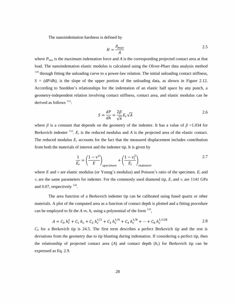
28
The nanoindentation hardness is defined by
2.5
where Pmax is the maximum indentation force and A is the corresponding projected contact area at that
load. The nanoindentation elastic modulus is calculated using the Oliver-Pharr data analysis method
110 through fitting the unloading curve to a power-law relation. The initial unloading contact stiffness,
S = (dP/dh), is the slope of the upper portion of the unloading data, as shown in Figure 2.12.
According to Sneddon‟s relationships for the indentation of an elastic half space by any punch, a
geometry-independent relation involving contact stiffness, contact area, and elastic modulus can be
derived as follows 111
:
√ √
2.6
where β is a constant that depends on the geometry of the indenter. It has a value of β =1.034 for
Berkovich indenter 112
. Er is the reduced modulus and A is the projected area of the elastic contact.
The reduced modulus Er accounts for the fact that the measured displacement includes contribution
from both the materials of interest and the indenter tip. It is given by
(
)
(
)
2.7
where E and ν are elastic modulus (or Young‟s modulus) and Poisson‟s ratio of the specimen. Ei and
νi are the same parameters for indenter. For the commonly used diamond tip, Ei and νi are 1141 GPa
and 0.07, respectively 110
.
The area function of a Berkovich indenter tip can be calibrated using fused quartz or other
materials. A plot of the computed area as a function of contact depth is plotted and a fitting procedure
can be employed to fit the A vs. hc using a polynomial of the form 110
,
2.8
C0 for a Berkovich tip is 24.5. The first term describes a perfect Berkovich tip and the rest is
deviations from the geometry due to tip blunting during indentation. If considering a perfect tip, then
the relationship of projected contact area (A) and contact depth (hc) for Berkovich tip can be
expressed as Eq. 2.9.
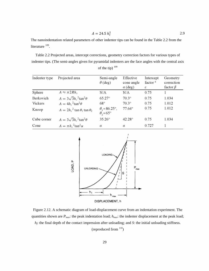
29
2.9
The nanoindentation related parameters of other indenter tips can be found in the Table 2.2 from the
literature 109
.
Table 2.2 Projected areas, intercept corrections, geometry correction factors for various types of
indenter tips. (The semi-angles given for pyramidal indenters are the face angles with the central axis
of the tip) 109
Figure 2.12. A schematic diagram of load-displacement curve from an indentation experiment. The
quantities shown are Pmax: the peak indentation load; hmax: the indenter displacement at the peak load;
hf: the final depth of the contact impression after unloading; and S: the initial unloading stiffness.
(reproduced from 110
)

30
2.1.3.2 Characterization of Ag Nanomaterials
There are large amount of works regarding nanoindentation characterization of nanomaterials
with in-situ or ex-situ techniques. Here only the silver materials are summarized, especially
nanoporous materials, regarding the characterization using nanoindenter. Generally, the peak
indentation depth is controlled less than 30% of thickness of the measured materials to reduce the
substrate effect on the measurement of the hardness and elastic modulus 113
.
In-situ TEM nanoindentation was carried out on silver nanoparticles to observe the
deformation and defects formation during compression in real time 114
. Silver nanoparticles were
affixed to a metal wire and against diamond tip. The indentation steps are shown in Figure 2.13. It
was observed that the strain on the nanoparticle caused several contrast bands (Figure 2.13b-e). After
unloading, the contrast bands vanished when the strain was removed (Figure 2.13f). Through
analyzing the possibility of which can cause these contrast bands, the localized strain near the core of
dislocations was determined. There is an attractive force between dislocations and free surface of
nanoparticles which can be changed because of the different strain energy when a dislocation moves
towards to the free surface. Both dislocations and elastic type artifacts in nanoparticle can contribute
to the absent of contrast bands when removing the strain. Under HRTEM, the revolution of
dislocations can be observed, see Figure 2.14. It is suggested that the dislocation occurs and becomes
more as the strain on nanoparticle increases. They are invisible when the indenter is removed finally.
It confirmed that the dislocation caused contrast can be observed. However, the mechanical properties,
such as hardness or elastic modulus, have not been shown in this work.

31
Figure 2.13 TEM image taken from the in situ nanoindentation experiment. (a) the probe and silver
nanoparticle before the nanoindentation. (b-e) during indentation, where contrast bands highlighted
with A-H. (f) the probe and nanoparticle after deformation. (reproduced from 114
)
Figure 2.14 HRTEM image of (a) silver nanoparticle before compression, the present twin is
highlighted; the (b) beginning and (c) middle of indentation, an edge dislocation is highlighted in the
inset; (d) after indenter is removed. (reproduced from 114
)

32
The mechanical properties of sintered nanoink silver films fabricated through spin coating
and thermal annealing were characterized by Greer et al. 115
. The typical microstructure and load-
displacement curve obtained for the film are shown in Figure 2.15a-b. To account for the effect of the
substrate when the indentation depth is larger than 30% of the film thickness, Greer et al. used the
method developed by Korsunsky et al. 116
to calculate the true film hardness from the measured value
Hmeas,
⁄ 2.10
where H is the respective harness (subscripts „Si‟ and „f‟ present Si substrate and silver film), h is the
indentation depth, and χ is the geometric parameter and t stands for the thickness of silver film. The
hardness of film and substrate composite based on Eq. 2.10 and the measured data are shown in
Figure 2.15c. Consequently, the average hardness was 0.91 GPa for the sintered nanoink silver films
with a 50 nm particle size, which is half of the hardness of a corresponding nanocrystalline silver film
with a 50 nm gain size, being 1.8 GPa 115
. The average elastic modulus was 110 GPa which is lower
than the value of 148 GPa reported by Panin et al. 117
due to the incomplete sintering of silver
nanoparticles.

33
Figure 2.15 a EM image of solution-derived nanoparticle silver ink thin films sintered at 150 C for
5-min. (b) Nanoindentation load-displacement curve for nanoink silver film on a Si substrate. (c)
Indentation hardness as a function of fractional indentation depth. (reproduce from 115
)
Recently, the inkjet-printed silver nanoporous films have also been studied by Dou et al. 118
.
The effect of nanoparticle size (ligament thickness) was investigated. By applying known relative
density (ρfoam/ρligament) and measured apparent strength (σfoam) of silver foam, the strength of
nanoporous materials can be calculated with the following expressions 32, 119
.
( ) ( ( ))
( ) 2.11
( )
( ) 2.12
where l* represents the length of ligament loaded in shear and t is the thickness of ligament. Table 2.3
shows these calculated ligament yield strength of sintered nanoporous silver films and other
properties. The ligament strength show very high values, up to 1 GPa when the ligament size is 80 nm
which is greater than the strength of bulk polycrystalline, that increases with decreasing the ligament
size 118
. This work shows an obvious nano size effect on mechanical behavior of silver. The
nucleation of Shockley partial dislocations and deformation twins in micro scale accounts for the high

34
strength. However, the scaling relation of strength for nanoporous silver is not well discussed and the
evolution of deformation microtwins is still unclear as well.
Table 2.3 Physical properties of inkjet-printed silver nanoporous layers after sintering for 24 h at
different temperatures 118
.
Flat punch nanoindentation has been performed on silver micro pillars to investigate the
deformation behaviors by Buzzi et al. 120
. They suggested that deformation localized at twin
boundaries which are formed due to the dislocation slip on (111) plane. The dislocation and
deformation twinning were caused by the low stacking fault energy of silver. The inverse dependence
of strength on the diameter of pillars is presented. However, pillar diameter is in submicron level and
not reach 100 nm and below. The study of if the deformation behavior of nanopillars (and/or
nanowires) follows the same process is needed to understand the nano size effects on mechanical
properties of silver nanomaterials.
A nanoindentation study on silver nanowire with 4 μm long and 42 nm in diameter conducted
by Li et al. 111
is shown in Figure 2.16. The AFM images and height profile were employed to
calculate the indentation projected areas since the wire is curved which is different with the
circumstance of flat surface usually involved. There is a step (or namely pop-in mark sometimes) in
the loading curve, see Figure 2.16d. The loading curve before the step was used to calculate the
elastic modulus using Hertzian elastic contact mode. The fitting result indicated the elastic modulus
of silver NW is 88 GPa. The hardness is about 870 MPa. These two values are in good agreement
with the nanoindentation results of bulk silver single crystal 111
. They also suggested that the step on
loading curve was attributed to beginning of plastic deformation associated with the dislocation
nucleation and motion 121
. The nucleated dislocations led the indentation more difficult afterward and
increased the slop of loading curve.

35
Figure 2.16 (a,b) AFM images of indents on silver nanowires after nanoindentation; (c) height profile
of an indent on the wire and (d) a representative nanoindentation load-displacement curve.
(reproduced from 111
)
2.2 Joining of Ag Nanomaterials
Similar to classified features and terminologies in regular welding and microjoining, the
current joining methods for nanomaterials can be divided into three categories on the basis of the
physical state of base components: fusion welding, solid-state joining, brazing and soldering. When
the size of joining components shrinks to nano scale, nano size effect can stimulate the low
temperature joining process. Regarding silver nanoparticles, this low temperature joining process has
been applied in electronics packaging industry to replace the micro silver flack pastes. At present,
limited research has investigated low temperature joining of silver nanowires and its application for
flexible electronics packaging.

36
2.2.1 Basic Joining Concepts
At the macro and micro scale, various joining processes have been developed to fabricate
metallic interconnects for achieving good mechanical strength and electrical conductivity in bulk
materials. Roughly, they can be classified as three major types based on the physical states of the
parts to be joined: fusion welding, soldering/brazing, solid-state bonding 122
.
In general, fusion welding processes involving the high heat input and high temperatures
using various energy sources, including laser 1-3
, electron beam 123
, electrical resistance 6, plasma
124,
microwave 125-127
and chemical reaction 128
, which all cause local melting of the base building blocks.
In terms of soldering and brazing, important methods of joining materials without melting the base
components, molten filler metal is introduced between the base components for their metallurgical
reaction which includes the dissolution process of the solid base metal into molten liquid and then
formation process of a reaction layer between them 13, 129
.
Among brazing and soldering, the filler metals typically have low liquidus temperatures (<
450 oC) in soldering, and originally contained lead which raised many concerns due to health,
environmental and safety issues worldwide. Presently, even the well-developed lead-free soldering
technology 130-133
, where the general melting point of filler metals ranges from 200 to 300 oC, is still
insufficient to satisfy the requirement of interconnection of heat-sensitive substrates, thus restricting
the popularization of flexible electronic or organic light-emitting devices 11, 134, 135
, and ferroelectric
materials with low transition temperature or organic ferroelectric materials 136-138
.
As solid-state bonding processes, friction welding 139, 140
or ultrasonic wire bonding 141
will
introduce high strain and plastic deformation to the parts at near their melting temperatures. Solid-
state sintering or even diffusion bonding of bulk materials, are typically carried out in an inert
atmosphere or vacuum, and involve temperatures at least over half of the melting point, with
pressures between 1 to 10 MPa 142
. The bond formation generally takes place in two phases, first
where a partial bond is formed and the asperities between the components begin to collapse with
residual porosity between the joined asperities. Then a complete bond is formed after prolonged times
at high temperatures such that diffusion and creep increase the contact area.

37
2.2.2 Size Effects on Low Temperature Sintering
Sintering occurs by migration of atoms mainly along the particle surfaces, suggesting that
surface energy and curvature would be the dominant factors for sintering. Surface energy, γ, is an
excess free energy and it is the reduction in surface area which drives the sintering process. It is
defined to be the energy to create a unit area of surface 143
.
The driving force at the interface when two spherical particles contact is given by the Laplace
equation,
(
) 2.13
where R1 and R2 are the principal radii of curvature at the contact point of the surface. P0 is the
pressure external to the surface and γ is the surface energy, γ=(∂G/∂A)T,P,n. The surface energy
includes the structural contribution due to surface stress derivation and surface chemical contribution
from the energy in breaking bonds related not only to curvature, but also to stress and composition 144
.
Therefore, the driving force for reduction of surface area will increase when the size of particles
decreases to nano scale.
Generally, the sintering process is controlled by sintering temperature and time. The sintering
temperatures of materials can be written as,
2.14
where Ts is the sintering temperature and Tm is melting temperature dependent on the material. The
factor α is dependent on material geometries and other environmental conditions. Thus, the effective
sintering temperature is contributed by two aspects, the coefficient α and melting temperature Tm.
Although sintering processes proceed without melting in most cases, the decrease of melting
temperature in nanoparticles (Tm) can contribute to the decreasing of sintering temperature compared
with bulk sintering. Based on modified versions of the Debye model for size dependence of melting
point 145, 146
, it can be shown that the sintering of nanoparticles is enhanced by the suppression of the
melting point Tm, which is reduced from that of the bulk material melting point (Tmb) by a factor as
follows 147, 148
:
(
) 2.15
where D is the particle diameter and δ is a material dependent parameter with reported values from
about 1.80 to 2.65 nm for various metals 15
, depending on the atomic volume and solid-vapor
interfacial energy 148
(related to the bonding energy of the crystal structure). Thereby, the Tm < Tmb for

38
nanoparticles contributes to a reduced sintering temperature. The other influencing factor α is usually
selected to be 0.8 for bulk materials 149
, (Ts = 0.8Tmb). However, the sintering of microparticles can
proceed at 0.5-0.8Tm 150-152
, while values of as 0.1-0.3Tm 150, 153
have been reported for nanoparticles
and Monte Carlo and molecular dynamic simulation show even lower temperatures down to a few
Kelvins 154-156
. The reduction of the influence factor from 0.8 to 0.3 is attributed to the larger driving
force for nanoparticles as previously mentioned and further reduces the sintering temperatures.
The sintering process in nanoparticles begins with rapid neck formation followed by neck
growth driven by surface diffusion, and then by vapour-condensation. Surface and grain-boundary
diffusion are the two main mechanisms throughout the entire sintering process, although dislocations
are present at the early stage of the sintering. Grain-boundary diffusion promotes the neck size growth
157 as illustrated in the numerical modeling results in Figure 2.17. Faster surface diffusion plus
evaporation condensation at higher temperatures are also among the factors promoting faster neck
size growth.
Figure 2.17 MD simulation of two large particles sintering at T = 63% Tm. (a-d) without grain
boundary and (e-h) with grain boundary. Snapshots for the sintering process are t = 500, 50000,
200000 and 500000 steps. Every particle contains around 3000 atoms with bulk atoms (blue), surface
or grain boundary atoms (red) and vapour state atoms (cyan), respectively. (reproduced from 157
)

39
Currently, the sintering behaviors among individual spherical particles have been well
established 158-162
. The above model only describes the sintering behaviors between spherical
particles. However, materials with different shapes are rarely considered in studies of the sintering
behaviors. Since other shaped materials, such as fibers, belts and disks 156
, are different from the
spherical case, it may not be suitable for them. Therefore, starting from a small scale, the study of
nanosintering processes of different shaped nanomaterials could enrich the sintering theory.
2.2.3 Progress in Low Temperature Joining of Ag Nanomaterials
2.2.3.1 From Micro to Nano Pastes for Electronics Packaging
Since the late 1980s, electronics packaging has already employed Ag material pastes as a die
attach material 163
. Usually, the weight percentage of the metallic particles in the paste has been 70%
~ 80% 164
. The rest is composed of organic solvents, dispersant and polymer-based binders to increase
the material stability and processing ability. Rheology of the paste can be tuned by using different
surfactants and particle sizes 165-168
. Binders and dispersants serve the same function of dispersing the
particles and both terms have been often used interchangeably in literature 169
. They can prevent the
agglomeration of particles in the paste but will also restrain the sintering. Therefore, the reduction of
such organics can achieve lower sintering temperatures. Elevated temperatures are usually used to
remove the organics during the bonding process. Their release can generate voids after sintering as
well. Generally, sintering pressure, time, temperature, particle size and the surface condition of
substrates could influence the joint properties significantly. However, large pressures, typically above
10 MPa 163
, could be needed to achieve robust bonding, which may be unsuitable for practical
applications. Hence, various research efforts have been conducted to reduce the sintering pressure
during bonding processes.
It has been found that the surface diffusion coefficient increases with the decrease of
nanoparticle (NP) size suggesting a higher specific surface energy of NPs than that of the micro-
particles or bulk materials. Considering that the driving force for diffusion is inversely proportional to
the size of the particles as mentioned in Section 2.2.2, a high driving force results in a decrease in
sintering temperature of nanoparticles 170
. The suppression of melting temperature (as shown in
Eq.2.15) and existence of a surface premelting layer (as observed with molecular dynamic simulation
148, 171) will enhance the sintering of NPs. It also appears that smaller these NPs could be
interconnected under lower external pressure since the stresses at contact areas increase with reducing
NP size. Therefore, replacing micro-flakes with NPs will simultaneously induce low sintering

40
temperatures and required pressure, making low temperature joining feasible. For example, these
factors may make it possible for significant sintering to occur at less than one third of the melting
temperature of the materials, a temperature where traditional diffusion bonding of bulk materials is
not normally feasible 150
.
2.2.3.2 Application of Ag NP Pastes in Electronics Packaging
Currently, the leading application for sintered nanomaterial joints is for micro-electronic
packaging. The performance of sintered nanomaterial joints can be affected by various parameters
during bonding process, including temperature, time and pressure, and the qualities of nanopastes
(such as organic content in the paste, size and shape of nanomaterials). Usually, appropriate sintering
temperatures are chosen according to the application requirement and substrates used and the
sinterability of pastes. These factors depend on the types and contents of organic binders and
dispersant in the pastes, the different materials coated onto substrates and the materials of substrates
(such as, Ag/Au/Ni coated Cu, bare Cu, or Ag/Au coated plastics 16, 17, 172-175
).
2.2.3.2.1 Influence of Temperature during joining
The elevated sintering temperature can produce higher strength of sintered nanomaterial
joints due to more intense sintering between nanomaterials and nanomaterial to substrates. During
initial development of low temperature joining technology, the sintering temperatures ranged from
250 to 350 oC since a significant amount of polymers were added into the pastes to improve the
stability of nanopastes and coating properties on substrates. Sintering temperatures have subsequently
been reduced to below 200 oC successfully after many efforts, as shown in Figure 2.18. For example,
PVP coated Cu NPs were introduced into the paste to replace Ag NPs and achieved bonding at 170 oC
18. An in-situ transformed Ag NP from the Ag2O method has been invented by Hirose et al.
174, 176 in
order to bond Cu substrates, in which the paste contained a large amount of organics to support the
reaction of Ag2O and this reduced the bonding temperature to 180oC. The organics in the pastes of the
above two methods have been limited, thus further reducing temperatures. If the paste content
incorporates less organics, the bonding temperature could decrease to 150 oC or even lower with
further tuning of the particle size distributions, as demonstrated by Zou et al. 177
and Hu et al. 172
.
Although increasing temperatures clearly enhance diffusional bonding, coarsening and coalescence of
nanostructures also occur, which ultimately deteriorate the microstructure and disrupt the properties
which are enhanced at the nano scale.

41
Figure 2.18 Strength of joints bonded at different temperatures. (data from 18, 172, 174, 177
)
2.2.3.2.2 Influence of Time during joining
Time is another factor controlling the sintering process and will affect the joint strength
eventually. At the same sintering temperature, longer sintering time could allow the organics or
solvents to decompose and more nanoparticles interconnect with their near neighbors to increase the
density of sintered nanomaterials and improve the joint strength. Figure 2.19 summarizes the joint
strength recorded at various sintering times from a few seconds to 60 minutes. A nearly linear relation
between strength and sintering time at 250 oC was reported by Hirose et al.
174 using in-situ formed
Ag NPs, as open squares plotted in Figure 2.19. At same time, the coarsening of nanoparticles must
be considered when the sintering time increases because grain growth instead of densification of
sintered nanomaterials naturally leads to lower joint strength 169
. Herein, higher sintering temperature
might be better to further improve the strength since it could help densify the sintered nanomaterials
due to the grain boundary and lattice diffusion of interconnected nanomaterials, which are also
referred to as densification mechanisms at higher temperature in the literature 169, 178
. For example,
using an external pressure of 5 MPa at 200 oC, the joint strength increased from 28 MPa to around 35
MPa when sintering time was increased from 5 to 30 min 175
. However, when the temperature
increased to 275 oC, 40 MPa was recorded after only 1 min of sintering at the same pressure
179.

42
Figure 2.19 Strength of joints bonded with Ag nanomaterials at different sintering times. (data from
16, 174, 175, 178-182)
2.2.3.2.3 Influence of pressure
When the particle size decreases to the nanoscale, the sintering pressure between two
contacting spherical particles will increase as suggested in Section 2.2.2. The application of external
pressure during a sintering process could enhance this sintering pressure and also help densify the
sintered nanomaterials and improve the joint strength. Figure 2.20 illustrates the influence of bonding
pressure on the joint strength. From the work of Morita et al. and Yan et al. 175, 183
, the strength
exhibited a significant increase when the bonding pressure increased from 0 to 5 MPa at 250oC and
300oC. However, increases in bonding pressure to 10 MPa provided limited improvement in the
strength 183
. This threshold bonding pressure of 5 MPa has been reported when the sintering
temperature is 275 oC by Lei et al. as well
169, 180. It has been found that this threshold pressure is also
dependent on particle size 180
. However, a direct correlation between particle size and threshold
pressure is difficult to establish by theoretical modeling since a wide distribution in particle size and
irregular particle geometries in experimental studies complicate this issue. Although the bonding
pressure has been dramatically decreased using Ag NPs instead of Ag microflakes, the ideal
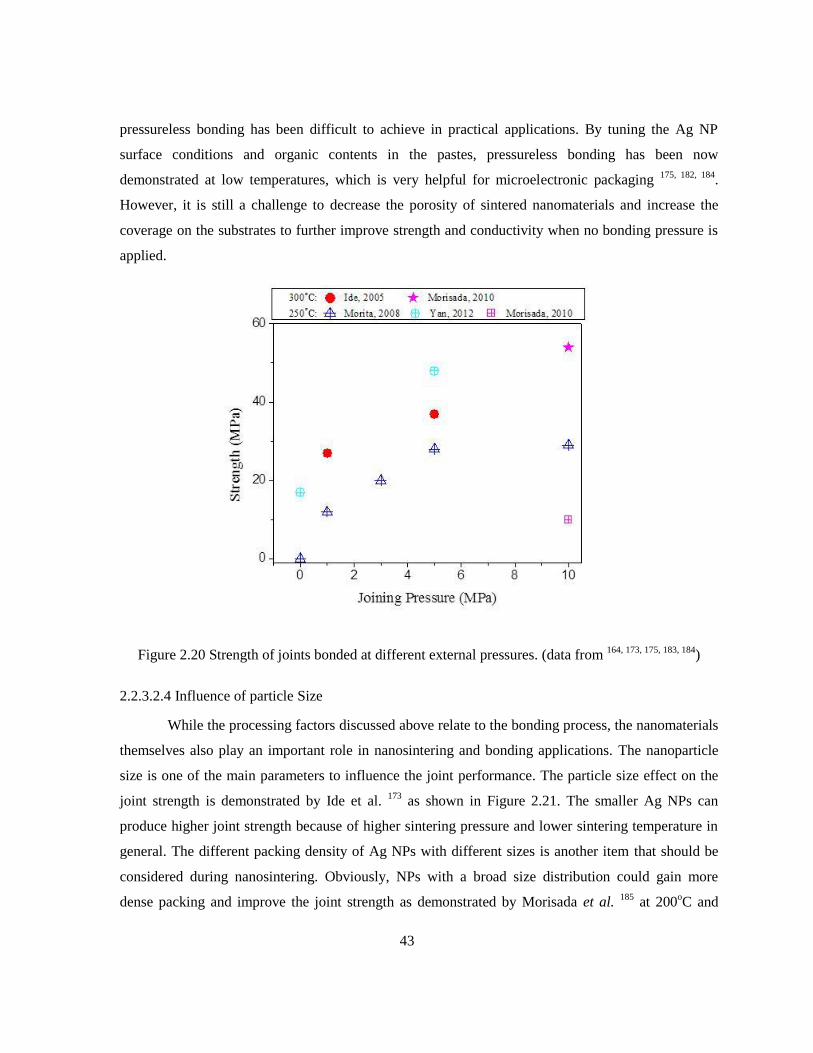
43
pressureless bonding has been difficult to achieve in practical applications. By tuning the Ag NP
surface conditions and organic contents in the pastes, pressureless bonding has been now
demonstrated at low temperatures, which is very helpful for microelectronic packaging 175, 182, 184
.
However, it is still a challenge to decrease the porosity of sintered nanomaterials and increase the
coverage on the substrates to further improve strength and conductivity when no bonding pressure is
applied.
Figure 2.20 Strength of joints bonded at different external pressures. (data from 164, 173, 175, 183, 184
)
2.2.3.2.4 Influence of particle Size
While the processing factors discussed above relate to the bonding process, the nanomaterials
themselves also play an important role in nanosintering and bonding applications. The nanoparticle
size is one of the main parameters to influence the joint performance. The particle size effect on the
joint strength is demonstrated by Ide et al. 173
as shown in Figure 2.21. The smaller Ag NPs can
produce higher joint strength because of higher sintering pressure and lower sintering temperature in
general. The different packing density of Ag NPs with different sizes is another item that should be
considered during nanosintering. Obviously, NPs with a broad size distribution could gain more
dense packing and improve the joint strength as demonstrated by Morisada et al. 185
at 200oC and
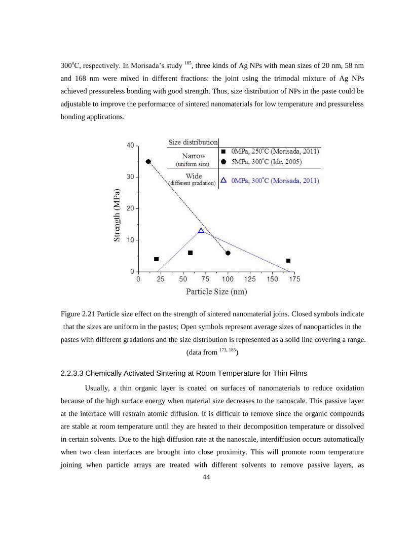
44
300oC, respectively. In Morisada‟s study
185, three kinds of Ag NPs with mean sizes of 20 nm, 58 nm
and 168 nm were mixed in different fractions: the joint using the trimodal mixture of Ag NPs
achieved pressureless bonding with good strength. Thus, size distribution of NPs in the paste could be
adjustable to improve the performance of sintered nanomaterials for low temperature and pressureless
bonding applications.
Figure 2.21 Particle size effect on the strength of sintered nanomaterial joins. Closed symbols indicate
that the sizes are uniform in the pastes; Open symbols represent average sizes of nanoparticles in the
pastes with different gradations and the size distribution is represented as a solid line covering a range.
(data from 173, 185
)
2.2.3.3 Chemically Activated Sintering at Room Temperature for Thin Films
Usually, a thin organic layer is coated on surfaces of nanomaterials to reduce oxidation
because of the high surface energy when material size decreases to the nanoscale. This passive layer
at the interface will restrain atomic diffusion. It is difficult to remove since the organic compounds
are stable at room temperature until they are heated to their decomposition temperature or dissolved
in certain solvents. Due to the high diffusion rate at the nanoscale, interdiffusion occurs automatically
when two clean interfaces are brought into close proximity. This will promote room temperature
joining when particle arrays are treated with different solvents to remove passive layers, as

45
demonstrated in Figure 2.22. At present, the solvents used in the reported methods involve two main
categories, cationic polymers and electrolyte solutions. For example, poly-diallyldimethylammonium
chloride is the one of the polymers used in Magdassi et al.‟s study 186
. Solutions of NaCl, MgCl2 and
CaCl2 were adopted to trigger the sintering of Ag NPs as well 187-189
. However, the mechanism for
removal of organics in these solvents is unclear at this moment. In general, all these usable solvents
contain Cl-1
to help desorption of protective organics on the surfaces. However, Cl-1
or other ions will
also leaveresidue on the nanomaterials surfaces significantly influencing their chemical properties.
Changes in the shape of Ag NPs may also occur after immersing them into solutions with high
concentrations of ions. Further, this approach is not area selective since the entire surfaces would be
exposed after removing the organics. However, it will be a potentially efficient and programmable
method to fabricate conductive films or electrodes due to the complete removal of organics.
Figure 2.22 (a) Schematic illustration of chemically activated joining using cationic polymer or
electrolyte solution. The microstructure of Ag NPs before (b) and after (c) applying cationic polymer.
(reproduced from 186-189
)
2.2.4 Joining of Ag NWs
At present, there are many attempts on joining of metal nanowires, such as end-to-end joining
of gold nanowires by reflowing tin solder 7, 190, 191
, butt or lap welding of platinum nanowires by Joule
heating 192
, end-to-side joining of gold nanowire with platinum-cobalt nanowire by tin-gold solder 6.
These methods all involved high heat energy and temperatures which can cause the melting of

46
nanowires or filler materials. Due to the nano size effect, the nanomaterial shape or surfaces will be
more active during heating because of surface energy effects on the melting points and thermal
sensitivity. During the heating process, it is difficult to maintain the original structure and shape of
nanowires, especially when nanowires are melted. However, the shape and size of nanomaterials are
two key factors which are vital for fully exploiting their properties. Thus, more precise and
controllable low temperature or even room-temperature sintering or joining methods are required. As
mentioned previously, when the interconnection area, the required energy for promoting diffusion to
form atomic level bonds will be reduced dramatically. Therefore, only a small amount of energy is
needed for joining two nanomaterials, and joining may even occur by surface diffusion without
external energy to trigger. Recently, Lu et al. found that end-to-end joining of gold nanowires by
oriented attachment at room temperature11
. Here, two recently developed room temperature joining
methods developed for silver nanowires are reviewed.
2.2.4.1 Optical Welding: Localized Plasmonic Heating
Light will induce heating of materials due to absorption of radiation, e.g. pulsed lasers with
high energy density may induce rapid heating and melting in a short time. This energy source requires
improve control for welding of nanomaterials. Recently, the use of a tungsten 9 or xenon
193, 194 lamp
was demonstrated in fabricating large area transparent conductive thin films. Garnett et al. 9 explained
this as a self-limited plasmonic welding method to create nanojunctions of Ag NWs, as shown in
Figure 2.23 a-c. In this scenario, by using the plasmonic effect of silver, a low density of light will
concentrate at the gaps between two adjacent nanoobjects, and these areas are referred to as hot-spots.
This concentration of light can induce a high temperature locally without heating the surroundings as
suggested in the simulated results in Figure 2.23d. Thus, local melting can occur and form metallic
bonds at the interfaces, keeping the rest of the nanowires with their original shape. However, it is not
an area specific method and joint quality will depend on the lighting time and light intensity, interface
geometries and the separation distances between nanomaterials because of the limited size of the hot-
spots. Nevertheless, selective plasmonic welding might be interesting for nanodevice fabrication in
the future. Liu et al. 195
has reported that femtosecond laser induced plasmon excitation could be
locally controlled in one single silver nanowire, in which local heat will be a useful source for
controllable selective joining of individual silver nanowires.
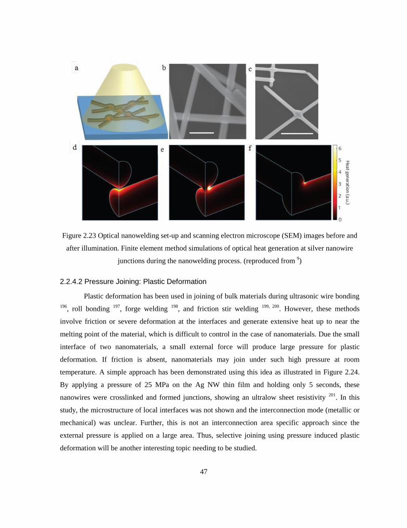
47
Figure 2.23 Optical nanowelding set-up and scanning electron microscope (SEM) images before and
after illumination. Finite element method simulations of optical heat generation at silver nanowire
junctions during the nanowelding process. (reproduced from 9)
2.2.4.2 Pressure Joining: Plastic Deformation
Plastic deformation has been used in joining of bulk materials during ultrasonic wire bonding
196, roll bonding
197, forge welding
198, and friction stir welding
199, 200. However, these methods
involve friction or severe deformation at the interfaces and generate extensive heat up to near the
melting point of the material, which is difficult to control in the case of nanomaterials. Due the small
interface of two nanomaterials, a small external force will produce large pressure for plastic
deformation. If friction is absent, nanomaterials may join under such high pressure at room
temperature. A simple approach has been demonstrated using this idea as illustrated in Figure 2.24.
By applying a pressure of 25 MPa on the Ag NW thin film and holding only 5 seconds, these
nanowires were crosslinked and formed junctions, showing an ultralow sheet resistivity 201
. In this
study, the microstructure of local interfaces was not shown and the interconnection mode (metallic or
mechanical) was unclear. Further, this is not an interconnection area specific approach since the
external pressure is applied on a large area. Thus, selective joining using pressure induced plastic
deformation will be another interesting topic needing to be studied.

48
Figure 2.24 Ag NW film: before (a) and after (b) applying 25 MPa pressure for 5 seconds.
(reproduced from 201
)
2.3 Problem Summary
From above review, it can be found that previous research on low temperature joining process
is mainly for nanoparticles rather than different shaped nanomaterials. The joining process is still with
the assistance of external pressure (~5 MPa) and heat (~200 oC). The understanding of nano size
effects on joining process is still incomplete, and it remains unclear whether the joining process can
be completed without external pressure and heat. On the other hand, there are little published papers
on mechanical behavior of silver nanoporous materials. The majority of research on mechanical
properties of silver nanowire are based on tensile testing through in-situ SEM/TEM and molecular
dynamics simulations, and three-point bending testing, which are all have their own drawbacks. At
present, the mechanical properties of silver nanowires are focused on individual nanowires. There is
very limited research on the practical application of them. In practice, their mechanical behavior
under loading is still lacking of understanding. Therefore, more work on low temperature or even
room-temperature joining of silver nanowires and their mechanical behaviors on loading are expected
to be done in these areas.

49
Chapter 3
Joining of Individual Silver Nanowires*
3.1 Introduction
With the extensive study of nanoelectronic devices and nanoelectromechanical systems
(NEMS), nanointerconnections have become a necessity for extremely dense logic circuits 11
. Bottom-
up assembly of metallic one-dimensional (1D) nanostructure is one of the most efficient methods to
construct nanocircuits. Silver nanowires (Ag NW) have attracted considerable interest because of
their excellent electrical conductivity and mechanical properties. Although some methods such as
soldering 6, 7, 191
, voltage and/or current excitation 4, 192, 202, 203
, thermal sintering 204, 205
, electron beam
irradiation 206-208
, laser irradiation 209, 210
and plasmon interaction 9 have been successfully used to
create nanojunctions, local heating of some form is a general feature of these nanoscale welding
techniques. As the size range transitions to the nanoscale, an increasing surface to volume atomic
ratio 211
in the nanostructured materials enhances their sensitivity to heat. However, local heating is
often detrimental to the properties of the base material or damage the underlying substructures. In
addition it is difficult to precisely control the application of heat at the nanoscale. Due to these
limitations, joining of Ag NWs without heating is essential to engineer nanocircuits, and would be
considered an attractive technical solution for the electronic industry. Lu et al. 11
has demonstrated
cold welding of nanowires is possible by simply contacting two gold nanowires, such that surface-
atom diffusion and oriented-attachment leads to successful welding. In the case of Ag NWs with
highly oriented crystal structure produced by synthesis from a polyol solution 70
, this joining
mechanism is generally precluded due to the layer of residual polyvinylpyrrolidone (PVP) that
remains on the surface of the nanowires, thus the spontaneous cold welding mechanism has not been
reported for Ag NWs. However, if the protective organic layer is removed then one could readily
achieve this oriented attachment and promote cold welding of Ag NWs if the surface is activated.
This is mainly driven by the high surface to volume atomic ratio of the NW ends which enhances
atom diffusion as shown in the simulated results of Pereira and da Silva 10
.
In this study, nanojunctions between individual Ag NWs with five-fold symmetry are created
by following the surface activation. Through high-resolution transmission electron microscope
(HRTEM) and selected area electron diffraction (SAED), the phase relationship and joint formation
* Portions of this study also appear in: Peng, P., et al., Self-Oriented Nanojoining of Silver Nanowires via
Surface Selective Activation. Particle & Particle Systems Characterization, 2013. 30(5): p. 420-426.

50
mechanism between Ag NWs have been investigated. The phase orientation between the two Ag
NWs in the joint has been analytically studied and explained based on the crystallography of the
oriented nanowires. These self-oriented welded regions revealed that a similar crystal orientation is
maintained between the nanowires, and the diffusion along the boundary contributes to the
nanojunction formation. Those oriented joints could exhibit same strength and electrical conductivity
as the rest of the nanowires 11
. These end-to-end Ag NW nanojunctions may be considered as having
potential applications in the future nanoscale electronic circuits 212
. Further, these monocrystalline V-
shaped or zig-zag silver prisms terminated by twin boundaries and free surfaces may be a novel
structure for investigating the transport of electrons, light and vibrations in curved Ag NWs.
3.2 Experimental
3.2.1 Synthesis of Ag NWs
Ag NWs were prepared in a polyol solution with polyvinylpyrrolidone (PVP) as a structure
directing reagent using a method modified from the literature 66, 67
. In this study, 330 mg
polyvinylpyrrolidone or PVP ((C6H9NO)n, K25, M.W.= 24000, Alfa Aesar) and 12.5 mg silver
chloride (AgCl, Alfa Aesar) were mixed with 40 ml ethylene glycol (EG, Fisher Chemical) and was
heated to 170 oC. Then, 110 mg silver nitrate was dissolved in 10 ml ethylene glycol and added into
the mixed solution while stirring vigorously and continuing the reaction conditions for 1 hour.
3.2.2 Surface Activation Process
Three 10 ml as-synthesis Ag NW solutions were diluted to 50 ml using deionized (DI) water,
ethanol and acetone, respectively. These diluted solutions sonicated for 5 minutes and centrifuged at
3000 rpm to remove the supernates and collect Ag NWs. This process was repeated twice.
3.2.3 Characterization of Ag NWs
Optical microscopy (Olympus BX 51M, Japan) and Field-emission scanning electron
microscope (FE-SEM, Zeiss LEO 1530/1550 Gemini, Germany) were used to study the
microstructure of washed samples. Organic shells of Ag NW before and after washing and the
diffraction pattern of Ag NWs were observed using high resolution transmission electron microscopy
(HRTEM, JEOL 2010F, Japan).
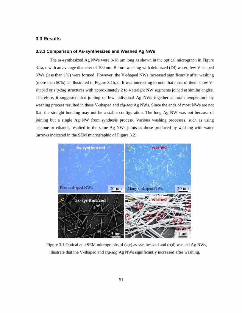
51
3.3 Results
3.3.1 Comparison of As-synthesized and Washed Ag NWs
The as-synthesized Ag NWs were 8-16 μm long as shown in the optical micrograph in Figure
3.1a, c with an average diameter of 100 nm. Before washing with deionized (DI) water, few V-shaped
NWs (less than 1%) were formed. However, the V-shaped NWs increased significantly after washing
(more than 50%) as illustrated in Figure 3.1b, d. It was interesting to note that most of them show V-
shaped or zig-zag structures with approximately 2 to 4 straight NW segments joined at similar angles.
Therefore, it suggested that joining of few individual Ag NWs together at room temperature by
washing process resulted in these V-shaped and zig-zag Ag NWs. Since the ends of most NWs are not
flat, the straight bonding may not be a stable configuration. The long Ag NW was not because of
joining but a single Ag NW from synthesis process. Various washing processes, such as using
acetone or ethanol, resulted in the same Ag NWs joints as those produced by washing with water
(arrows indicated in the SEM micrographic of Figure 3.2).
Figure 3.1 Optical and SEM micrographs of (a,c) as-synthesized and (b,d) washed Ag NWs,
illustrate that the V-shaped and zig-zag Ag NWs significantly increased after washing.

52
Figure 3.2 SEM images of (a) pristine Ag NWs in EG and after washing with (b) water, (c) acetone
and (d) ethanol.
3.3.2 Effects of Ultrasonication and Centrifugation
To check if ultrasonication may contribute the energy input and form V-shaped NWs, the
controlled experiment with different ultrasonication time and level was conducted, see Figure 3.3. It
could be seen that the proportion of V-shaped NWs did not show significant variation. Therefore, the
ultrasonication time and level did not largely promote nanojoint formation because the contact
opportunity between nanowires was quite low. However, the nanojoints could be widely observed in
the separated nanowires after centrifuging. Considering nanowires are separated from solution and
gather together on the bottom of tubes, the contact opportunity of these nanowires dramatically
increased and it might be one of the key parameters to control the joining. If nanowires have been
separated from solution, the centrifuge time and speed also have no strong relation with joining
proportion. It is worth noting that external pressure during the centrifuge process might promote
surface atom diffusion once two wires contacted. Even though the external force acted on each
nanowire is very weak, the stress/pressure is quite high because of the small contact area at the
nanowire interfaces between two ends in contact. Therefore, this immense stress localization created
between the ends of the nanowires during centrifuge process might be a considerable point for the
nanojoint formation in this case. These points will be discussed in a later section.
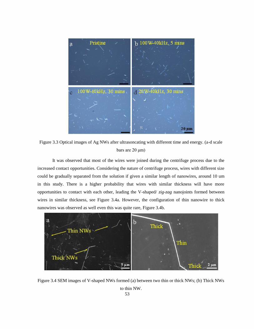
53
Figure 3.3 Optical images of Ag NWs after ultrasoncating with different time and energy. (a-d scale
bars are 20 μm
It was observed that most of the wires were joined during the centrifuge process due to the
increased contact opportunities. Considering the nature of centrifuge process, wires with different size
could be gradually separated from the solution if given a similar length of nanowires, around 10 um
in this study. There is a higher probability that wires with similar thickness will have more
opportunities to contact with each other, leading the V-shaped/ zig-zag nanojoints formed between
wires in similar thickness, see Figure 3.4a. However, the configuration of thin nanowire to thick
nanowires was observed as well even this was quite rare, Figure 3.4b.
Figure 3.4 SEM images of V-shaped NWs formed (a) between two thin or thick NWs; (b) Thick NWs
to thin NW.

54
3.3.3 Joint Selection
It was found that every part of the V-shaped NW was with the similar length as synthesized
NWs by measuring the length of NWs. There were few defects, for example stacking faults, within
the junction region according to the observation under TEM (this will be shown in details later),
indicating it was not a deformed NW but joined. Usually, the deformed structure would prefer to
show one continuous curve as the outer surface of NW indicated in Figure 3.5a. However, two
severely curved surfaces with V-shaped notches in the NWs further suggested that they were not
deformed by bending, see Figure 3.5b. Thus, it was believed that the majority of these V-shaped or
zig-zag Ag NWs was not formed by bending but by joining. During angle measurement, those NWs
with sharp corners as illustrated in Figure 3.5b were considered.
Figure 3.5 Difference of (a) bending with one continuous curve, and (b) joining with sharp corner and
two curved surfaces with small V-notch.
3.3.4 Angle Measurement and Distribution
To make sure the measured angle of joints was close to the actual angle, those v-shaped NWs
laid flat on the substrates and not intersected with others were selected. Thus, the concentration of
NWs on substrates was very low for measurement in this case. Large portions of NWs in optical
images laid flat on the substrate, making the angles were easy to measure. In addition, optical
microscope might be better for counting angels because it has larger visual field than SEM.
Therefore, most of those angles in this study were measured using optical images (500+
measurements in total). To investigate whether the V-shaped or zig-zag Ag NWs observed in optical

55
microscope (OM) could have different angles under SEM because of the diffraction limit of optical
microscopy, the same nanowires were observed and measured in both SEM and OM. The results were
compared and confirmed no difference for angle measurement as shown in Figure 3.6 (all compare
results are listed in Table 3.1). It suggests that even the diameter of the nanowire in optical
microscopy is several orders larger than its actual size, the angles between nanowires measured in
optical microscope are the same as in SEM. Therefore, it is believed that the angle distribution
measured under optical microscope is precise and truthful.
Figure 3.6 (a) Optical and (b) SEM micrographs of a bonded V-shaped Ag NWs (with 117o angle)
laid flat on Si substrate. (c) High magnification of the V-shaped Ag NWs with two curved surfaces
and a V-shaped notch in the joint region.
Table 3.1 Measured angles of exactly the same Ag NWs with optical microscopic image (OM) and
SEM image (SEM)
Measured Angles (o)
OM 126 119 119 116 137 141 124 143 131 97 127 123 127 128 113 133
SEM 128 120 118 117 137 141 122 141 135 96 128 118 129 129 109 135
When the angles of joints are plotted as a function of the frequency as shown in Figure 3.7a,
the distribution of angles concentrates in a narrow range of 121 to 130o. The typical morphology of
such Ag NW joints is illustrated in the TEM micrograph in Figure 3.7b, where an angle of 125o is

56
observed. It is worth mentioning that the interior angle of the joint is sharp, because there is a large
driving force for diffusion due to the high surface energy present at this location, while the outer
surface has a larger radius or curved structure because the driving force for diffusion is low. This
further supports the idea that these are joined, and not deformed wires because the outer surface of a
deformed wire would be one continuous curve (not two curved surfaces as shown in Figure 3.7b).
These structures differ from the previously reported V-shaped Ag NWs which formed due to twinned
crystal plane induced growth and crystal lattice match induced fusion during polyol-thermal synthesis
process 212, 213
. It should be noted that these nanojunctions were formed at room temperature after the
washing process without any heat input.
Figure 3.7 (a) Angle distribution of Ag NW joints. (b) TEM images of typical Ag NW joints.

57
3.4 Discussion
3.4.1 Selective Surface Activation
For fcc metals, surface energy of different faces is uniform, and mainly depends on the
variable density of atoms on each face 214
. In terms of silver, the surface atom density between the
100 and 111 planes is 1.2 × 10¹⁹
vs. 1.38 × 10¹⁹
atoms/m2, respectively
215. Consequently, the
relative surface energies of the low-index crystallographic planes are γ111 < γ100. Due to the stronger
interaction between PVP and 100 facets than that between PVP and 111 facets resulting from the
higher surface energy, it functions as a structure directing reagent on the surface of Ag nanomaterials
during synthesis. Xia and co-workers identified that the end of Ag NW with five-fold cross-section is
covered by 111 facets and with sides corresponding to 100 facets67
. The weak interaction of PVP
with the end facets of 111 leads to the higher chemical potential and reactivity on the ends, while
the adsorption of PVP on side surfaces of 100 is very strong and results in complete coverage 66
.
TEM images in Figure 3.8a&b support this notion, and demonstrate that the organic shells have a 2.5
nm and 5 nm thickness on the ends and sides of as-synthesized Ag NW respectively.
Once these Ag NWs intersect, this organic layer originating from the synthesis process could
be presented at the interfaces of the nanowires and influence the interdiffusion of atoms to facilitate
joining of Ag NWs without assistance of external energies, such as heat and pressure. Although the
PVP absorbed on the surfaces of Ag NWs does not readily decompose at below 300 oC
216, 217, the
majority of this organic compound would efficiently be removed during the process of washing with
DI water. Figure 3.8c&d indicate the organic shell reduced to 0.5 nm on the end and 2 nm on the
side of the Ag NWs after washing. Meanwhile, some areas on the ends of Ag NW were completely
devoid of organic coating as indicated in Figure 3.8c. These bare sites provide excellent
interdiffusion channels between two NWs in contact in an end-to-end manner, which will promote
spontaneous cold joining of Ag NWs due to the high driving force for surface diffusion at the
nanoscale. It worth noting that external pressure during the centrifuge process might promote surface
atom diffusion once two wires contacted. Even though the external force acted on each nanowire is
very weak, the stress/pressure is quite high because of the small contact area at the nanowire
interfaces between two ends in contact. However, the removal of PVP on the sides of Ag NW was not
significant and the relatively thick organic layer (compared to the ends), would likely inhibit
formation of a T-shaped joint (end-to-side). This suggests that the ends of the Ag NW have been
selectively activated for joining at room temperature and while keeping the rest of nanowire still

58
protected. This selective activation process is associated with washing and the specific facets (111) of
Ag NWs, indicating that it is not random but self-selective due to matching of crystal structures at the
ends of nanowires.
It is worth noting that long polymer chains, PVPs in this case, graft on the surfaces of the
nanowires and their presence could introduce repulsive secondary bonding forces between the two
counterparts as demonstrated during Ag nanocube assembly 218
. These forces would lead to a gap on
the order of few nanometers between the nanowires, impeding Ag atom diffusion as schematically
shown in Figure 3.8e, since this gap is too large to facilitate the transfer of surface atoms and
complete the diffusion process. The adsorption of polymer on the Ag surface also lowers the surface
energy, leading to an increase in the activation energy of surface atoms 219-221
. Further, the residual
polymers present in the gap between the nanowires could block the diffusion channels 222, 223
.
However, if only a small fraction of the polymer material remains on the surface, the repulsive effect
is reduced and the nanowire separation distance is much closer. Meanwhile, compared with large
fraction, a small concentration of polymer could provide higher surface energy and lower activation
energy of surface atoms to promote interdiffusion. Consequently, it promotes accelerated bonding
between two surfaces and allows two Ag NWs to easily form metallic bonds at room temperature.

59
Figure 3.8 TEM images of the end (a) and side (b) of pristine Ag NW; (c) and (d) washed Ag NW.
Some areas on the end of Ag NW were exposed without organic coatings as highlighted in the circles
in (c). Te breakage on the side of Ag NW is not significant in (d). (e) Schematic of assembly of Ag
NWs by modifying the surface of NWs with polymer chains grafts of different chain densities.
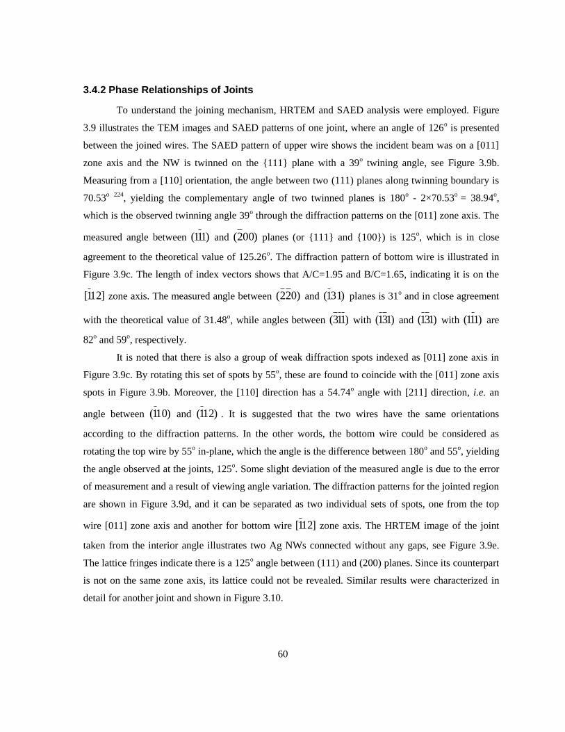
60
3.4.2 Phase Relationships of Joints
To understand the joining mechanism, HRTEM and SAED analysis were employed. Figure
3.9 illustrates the TEM images and SAED patterns of one joint, where an angle of 126o is presented
between the joined wires. The SAED pattern of upper wire shows the incident beam was on a [011]
zone axis and the NW is twinned on the 111 plane with a 39o twining angle, see Figure 3.9b.
Measuring from a [110] orientation, the angle between two (111) planes along twinning boundary is
70.53o
224, yielding the complementary angle of two twinned planes is 180
o - 2×70.53
o = 38.94
o,
which is the observed twinning angle 39o through the diffraction patterns on the [011] zone axis. The
measured angle between )111( and )002( planes (or 111 and 100) is 125
o, which is in close
agreement to the theoretical value of 125.26o. The diffraction pattern of bottom wire is illustrated in
Figure 3.9c. The length of index vectors shows that A/C=1.95 and B/C=1.65, indicating it is on the
]121[ zone axis. The measured angle between )022( and )311( planes is 31o and in close agreement
with the theoretical value of 31.48o, while angles between )113( with )131( and )131( with )111( are
82o and 59
o, respectively.
It is noted that there is also a group of weak diffraction spots indexed as [011] zone axis in
Figure 3.9c. By rotating this set of spots by 55o, these are found to coincide with the [011] zone axis
spots in Figure 3.9b. Moreover, the [110] direction has a 54.74o angle with [211] direction, i.e. an
angle between )101( and )121( . It is suggested that the two wires have the same orientations
according to the diffraction patterns. In the other words, the bottom wire could be considered as
rotating the top wire by 55o in-plane, which the angle is the difference between 180
o and 55
o, yielding
the angle observed at the joints, 125o. Some slight deviation of the measured angle is due to the error
of measurement and a result of viewing angle variation. The diffraction patterns for the jointed region
are shown in Figure 3.9d, and it can be separated as two individual sets of spots, one from the top
wire [011] zone axis and another for bottom wire ]121[ zone axis. The HRTEM image of the joint
taken from the interior angle illustrates two Ag NWs connected without any gaps, see Figure 3.9e.
The lattice fringes indicate there is a 125o angle between (111) and (200) planes. Since its counterpart
is not on the same zone axis, its lattice could not be revealed. Similar results were characterized in
detail for another joint and shown in Figure 3.10.
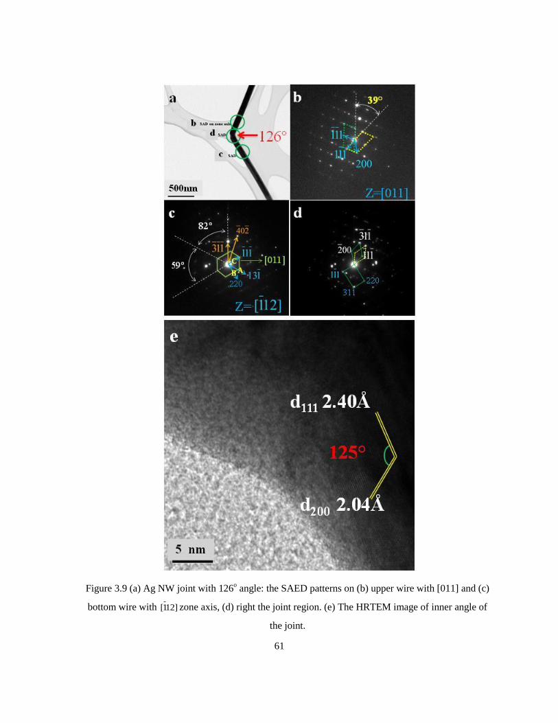
61
Figure 3.9 (a) Ag NW joint with 126o angle: the SAED patterns on (b) upper wire with [011] and (c)
bottom wire with ]121[ zone axis, (d) right the joint region. (e) The HRTEM image of inner angle of
the joint.

62
Figure 3.10 A typical joint of end-to-end Ag NWs: (a) TEM image of joint with a 126o angle; the
SAED patterns of (b), (c) and (d) corresponding to two wires and joint shown in (a).
The joints with smaller angles were also investigated to determine the orientation
relationships of these joints, such as 115o as depicted in Figure 3.11a. Figure 3.11b-c shows the
diffraction patterns corresponding to the [011] and ]121[ /[011] zone axis as previous observation.
Figure 3.11e displays the lattice fringes of the joint taken from exterior angle region, showing
distances of the (111) planes from two Ag NWs were 2.4Å and connected with a 10o misorientation.
The dashed circle highlights the defect contrast due to this misorientation. This 10o misorientation has
also appeared in diffraction patterns of the joint region as shown in Figure 3.11d. As indicated in the
angle measurements in Figure 3.7a, joints usually exhibit angles between 121 -130
o. Here, the
measured angle of two Ag NWs 115o in Figure 3.11a corresponds to a misorientation angle 10
o away
from the 125o angle expected between the orientation relationship proposed here. Therefore, it
suggests that the joints were formed by connecting two Ag NWs through lattice matching on (111)
planes. Further, the misorientation accounts for the fluctuating angles of these joints, in the range of
115 to 135o, as the statistical results suggested (see Figure 3.7a). The interfaces within 10
o
misorientation are low angle grain boundaries, resulting from the grain boundary diffusion in
conjunction with surface diffusion which dominates during joining. One could speculate that the two

63
wires tend to be self-oriented to strive towards lattice matching on (111) planes during these
diffusions.
Figure 3.11 (a) Ag NW joint with 115o angle: the SAED patterns on (b) left wire with [011] and (c)
right wire with ]121[ zone axis, (d) right the joint region. (e) The HRTEM image of exterior angle of
the joint, the (111) planes belong to two Ag NWs were matched with 10o mis-orientation. (The
dashed circle indicating the contrasts from defects because of the mis-orientation).

64
3.4.3 Joining Mechanism: Self-Oriented Nanojoining
Low stacking fault energy of silver materials promotes the crystal growth in nanosize, as a
result of twins 225
. In the case of Ag NWs, the twin boundaries run along the entire wire, and the Ag
NWs with five-fold cross-section could be considered as five highly orientated single Ag crystals
“triangular prisms”, highly oriented nanoscale grains 226
. Each single prism is coherently twinned
with another on the (111) plane and the end is covered by 111 facets. Joint formation has taken
placed on these two 111 facets of the end of Ag NWs, see Figure 3.12a. Here, the joint was actually
formed by the end of two single triangular prisms, and each of them was from the two joined wires.
Since the extremity of the triangular prisms were (111) plane, the joint interface was
(111)NW1//(111)NW2, or sometimes with a less than 10o mismatch. Therefore, a cleaned surface and
identical lattice orientations are required for self-oriented joining of Ag nanowires at room
temperature.
Considering the angle between 111 facets (on the end) and the axis of the NW is 54.74o,
the self-oriented joined NWs will not be straight. If two NWs connect with alignment such that the
centres of the pentagonal shapes (as labelled with red color region in Figure 3.12a) come into contact,
then the angle between two joined NWs with same orientations would be 2×54.74o=109.48
o. This is
an unfavourable angle as suggested in Figure 3.7a, and was not observed by TEM. It is worth noting
that the centre point of the NW is the intersection location of the five twin boundaries, suggesting it is
a high energy site as well. To minimize the energy of the system when two NWs contact, the edge-to-
edge configuration would be not preferred compared to centre-to-centre configuration. Actually, these
two configurations would be the same if two NWs have the same diameter, which would have low
possibility in reality. Conversely, “centre-to-edge” configuration of two NWs will allow the 111
lattices to easily match by NW rotation when the two end facets are not same size (two NWs with
different diameters) and introduce more contact edge sites between two NWs, yielding much larger
diffusion rate because the curvature of the NW decreases from the edge to the centre, see Figure
3.12b. In this case, centre-to-edge configuration could obtain around 50% higher energy edge sites
than that of centre-to-centre configuration (with the as assumed angle configuration), as red dashed
lines indicated in Figure 3.12b, leading to faster diffusion and nanojoining between centre-to-edge
aligned nanowire ends.
According to the lattice orientation relation of two Ag NWs, the atomic arrangement of the
joint is reproduced in Figure 3.12c. The atomic arrangement indicates that the lattices of two joined
“prisms” are well orientated and lattice matched. On each wire, the sides are terminated with a

65
coherent twin boundary and free surface, respectively. It suggests that this joint creates a V-shaped
prism with a monocrystalline structure. It is well accepted that the properties of crystals could be
influenced by defects such as such as grain boundaries and free surfaces. Here, the same orientated V-
shaped joint with two boundaries, a coherent twin boundary and free surface, may be a novel
candidate to investigate the homogeneous transport properties in nonlinear Ag NWs, for example
light/wave guidance and electronic transport of these joints. Furthermore, it has been shown that twin
boundary within the NW for fcc structure could produce anomalous strength and brittle fracture under
loading because the five twin boundaries in this type of NW were intersected with all of the possible
slip systems in fcc structure and the motion of dislocations is restricted by the twinning boundaries 227,
228. Consequently, they are effectively grain boundary hardened materials
226 while these Ag NW
joints with same orientations will be expected to gain good mechanical properties as that of original
individual Ag NW.
66
Figure 3.12 (a) Schematic illustration of end-to-end Ag NW joint, the cross-section of Ag NW is
five-folded. (b) Two facets with different sizes attached via centre-to-centre and centre-to-edge
configurations, letters H and L denote high and low diffusion sites belonging to different locations of
Ag NWs. (c) The atomic arrangement of Ag NW join, when view from a [110] orientation that is on
the coherent twin boundary with 70.53o angle of fcc Ag.
3.5 Summary and Remarks
In summary, the joining process and mechanisms during room temperature joining of
individual silver nanowires due to nano size effects have been presented in this chapter. A repeated
washing process was used to remove organics from the nanowire surfaces and selectively activated
the surface of the silver nanowires. This provided an interface free of contamination which enhanced
surface diffusion for nanojoining of silver nanowires end-to-end at room temperature.

67
Characterization of the joints by high resolution electron microscopy has revealed that a similar
crystal orientation was maintained between the nanowires and diffusion along the boundary
contributes to the nanojunction formation. A monocrystalline V-shaped or zig-zag silver prism was
formed after nanojoining, terminated by twin boundaries and free surfaces. The simple selective
activation process for nanojoining has potential applications for engineering electronic circuits, and
may represent a useful structure for investigating the transport properties of electrons, light and
vibration in bent silver nanowires.
This chapter has demonstrated that the end surface of Ag NWs could be activated with the
removal of the thin layer of PVP. These activated end surface would be ready for room temperature
joining due to nano size effect without external heat input; however it is only the small portions of the
entire surface of Ag NWs. The dominant side surface of Ag NWs is still difficult to activate. If the
organic layer on the side surface of the Ag NWs could be break down, the activated sites will increase
dramatically and raise the room temperature joining possibility subsequently. The formation of end-
to-side or side-to-side joining of Ag NWs will be able to push them into practical applications for
nano-circuits or lead to new applications. For example, largely activated surfaces of Ag NWs could
make three-dimensional networks feasible. These networks own excellent conductivities of silver and
good thermomechanical properties due to their porous structure. They may join with other metals at a
nano scale at room-temperature as well. These can make the silver nanowire networks as a good
interconnector candidate for flexible electronics benefitting by low processing temperature and good
thermal, electrical, mechanical properties. This study will be presented in next chapter.

68
Chapter 4
Joining Using Silver Nanowire Pastes†
4.1 Introduction
The atomic level interconnection of components to achieve metallurgical bonds is a key
requirement for micro/nano-electronic devices since conductive joints are needed in transistors 229-231
,
sensors 232, 233
, solar cells 234, 235
and display units 236-238
. Conventionally, external energy inputs are
needed to accelerate diffusion and mixing of atoms at the interfaces for metallic bond formation.
These excitation energies are generally applied through external sources during soldering & sintering
130, 173, laser welding
2, 239, 240, resistance welding
241, friction welding
242, 243, microwave sintering
244,
pressure welding 245, 246
, and delivered to the interfaces where connections are required. Generally, the
interfaces are mostly in bulk size and the energy requirements are large in these conventional joining
processes. Thermite welding is one category where heat is generated in-situ by an exothermic
reaction, however the process results in high temperatures which also melt the bulk material. When
the device and joint size reduce to micro- and/or nano-scale, the energy delivery should be more
precise, efficient and controllable. Meanwhile, some drawbacks will arise if the energy is still
delivered to the bulk surrounding material. For example, in the case of thermal heating, a typical lead-
free soldering process reaches 200 to 300 oC to obtain conductive joints
130, 247, which severely
restricts soldering for heat-sensitive components in electronic devices, such as flexible electronic
paper, organic light-emitting devices 11, 134, 248
and some ferroelectric devices containing inorganic
ferroelectric materials with low transition temperature or organic ferroelectric materials 136, 138, 249
.
Regarding laser sources, a beam diameter below 1 µm is difficult to achieve, and energy density
exponentially increases with decreasing beam size. Therefore, targeted energy delivery routes should
be developed to better control energies in a localized region without affecting surroundings for
micro/nano-electronic fabrication or flexible electronic device assembly.
Only a few new methods for delivering energy at the nanoscale for welding applications have
been reported, such as nanoscale soldering of individual gold nanowires by electrical welding using
metal solder 250
, and light-induced plasmonic local heating to archive nanojunctions of silver
nanowires 9. The former directly adopted Joule heating in a nanosized region while the latter
† Portions of this study also appear in: Peng, P., et al., Room-temperature pressureless bonding with silver
nanowire paste: towards organic electronic and heat-sensitive functional devices packaging. Journal of
Materials Chemistry, 2012. 22(26): p. 12997-13001.

69
concentrated photon energy onto a nanosized “hot-spot” region with the help of plasmonic effects to
generate heat locally. Similarly in these two methods, only a small amount of energy was delivered
and focused onto nanoscale areas to induce local melting and then facilitate nanojoining. It is worth
noting that one of the benefits at the nanoscale occurs in diffusion bonding of metallic nanomaterials,
allowing joining at relatively low temperatures or even room-temperature due to the increased surface
energy, sintering pressure and diffusion rates 13
when particle size is reduced < 100 nm. Thus, the
energy requirement for solid state joining at the nanoscale is very limited. Even room-temperature
joining without external energy input has been demonstrated by contacting two gold or silver
nanowires 11, 251
, where surface-atom diffusion and self-oriented attachment promotes nanojoining as
suggested in Chapter 3.
To date, low temperature interconnection processes using metallic nanoparticle paste was
demonstrated with silver 173, 182, 252
, copper 18
and gold 19
, and appears to be a promising alternative for
lead-free electronic packaging and flexible electronic interconnections 16, 172, 253, 254
. However, there is
no report of the use of nanowires as a filler material to form a bonded joint.
4.2 Experimental
4.2.1 Synthesis of Ag NW pastes
Ag NWs were prepared in a polyol solution with polyvinylpyrrolidone (PVP) as a structure
directing reagent using a method modified from the literature 66, 67
. In this study, 330 mg
polyvinylpyrrolidone or PVP ((C6H9NO)n, K25, M.W.= 24000, Alfa Aesar) and 12.5 mg silver
chloride (AgCl, Alfa Aesar) were mixed with 40 ml ethylene glycol (EG, Fisher Chemical) in a
round-bottom flask. The mixture was heated to between 160 and170 oC. Then, 110 mg silver nitrate
was dissolved in 10 ml ethylene glycol liquid and added into the mixed solution while stirring
vigorously and continuing the reaction conditions for 4 hours. The Ag NWs were condensed by
centrifugation at 4000 rpm using a 50 ml centrifuge pipe. The clean supernatants were removed from
the centrifuge pipes using a pipette resulting in highly concentrated Ag NW pastes.
4.2.2 Thermogravimetric Analysis
Ag NWs were washed by deionized (DI) water to remove the ethylene glycol and PVP and
condensed by centrifugation. Silver nanowire pastes with different washing processes were dried at
room temperature. To study the organic contents in the pastes, thermal gravimetric analysis (TGA)

70
was performed by heating these silver nanowire pastes from room temperature to 500 oC in air with a
heating rate of 5 oC/min.
4.2.3 Joining using Ag NW Pastes
Prior to joining, the copper wires with 0.25 mm thickness were cut into 60 mm pieces and
ultrasonically cleaned in acetone for 3 minutes to remove the organics, diluted HNO3 for 1 minute to
remove the oxide layer and rinsed in ultrapure water electrical resistivity approximately 18 MΩ·cm .
A fine needle attached on a 10 ml syringe was used to locate the Ag nanopaste between two clean
copper wires. After depositing 0.05 ml high concentrating Ag nanopaste, the assembly of copper
wires and paste was put at room-temperature (18 oC) or heated at 60~200
oC in air for 1 hour without
bonding pressure. Figure 4.1 illustrates the schematic diagram of the wire configuration during
joining process and joint size measurement.
Figure 4.1 Schematic illustration of (a) wire configuration during joining, (b) side-view and (c) cros-
section of Ag NW joint after heating. L and D denote the joining length and thickness of joint.
4.2.4 Tensile Testing
Tensile shear testing was conducted by loading the wires in the axial direction at a rate of 0.5
mm/min using a micro tensile tester (Instron 5548). Figure 4.2 shows the tensile shear test
configuration and joint failure. After clamping each bonded sample into the grips, loading was
applied. The measured strength of joints is the tensile shear strength due to the applied shear stress
during the tensile testing, because two Cu wires were not coaxial. It was estimated by dividing the
highest failure force value by the joining area, σ = Fmax/A (N/mm2 or MPa). The fracture area of

71
samples was difficult to measure due to the unsymmetrical geometry of fracture region. Here, the
average joining area was estimated to normalize the actual fracture area, which joining area A was
calculated by multiplying the maximum joining length L by thickness D of the Ag NW filler material.
Figure 4.2 Schematic illustration of tensile shear strength testing of bonded samples.
4.2.5 Nanoindentation
The mechanical properties of silver npm were tested with a depth-sensing nanoindenter
(Hysitron Triboindenter) equipped with a Berkovich tip. The tip was calibrated on fused silica.
Indentations were performed on the mechanically polished flat surfaces in a load controlled mode. All
nanoindentation experiments were performed using a constant loading rate of 60 μN/s, with loads of
600 μN. A minimum of 5 indents for each load were collected for each sample.
4.2.6 Resistivity Measurement
Resistivity of joint, ρ, was calculated using ρ=A×R/l, where resistance (R) was measured by
four probes low resistance Ohmmeter (DUCTER DLRO 10X), where A and l are the cross-section
area and length of the joint.
4.2.7 Microstructural Characterization
Field-emission scanning electron microscope (FE-SEM, Zeiss LEO 1530 Gemini, Germany)
were used to study the microstructure of interfaces and fracture surfaces of bonded samples. Energy-
dispersive X-ray spectroscopy (EDX, EDAX Pegasus 1200) was employed for elemental analysis. An
oscillating knife (DIATOM, Ultrasonic) in ultramicrotome was used to section the interfaces of room-

72
temperature bonded samples produced with Ag NW paste which was washed three times. The thin
slice with 100 nm in thickness was observed using transmission electron microscopy (TEM, PHILIPS
CM12) and high resolution transmission electron microscopy (HRTEM, JEOL 2010F).
4.2.8 Local Heat Measurement
The local heat measurement of Ag NW paste and copper substrate were conducted using two
methods. The Ag NW paste and Cu powder was mixed and immediately transferred into a crucible to
measure the temperature change from room-temperature to 60 oC using differential scanning
calorimeter (DSC, Netzsch, 404C) at 0.5 kpm air condition with heating rate of 0.5 oC/min. Home-
built data acquisition system was employed to measure the temperature change of Ag NW paste on
Cu substrate as shown in Figure 4.3.
Figure 4.3 Schemes of temperature testing configurations of (a) bare Cu substrate and (b) Cu-Ag NW
paste system at room temperature.
4.3 Results
4.3.1 Organic Content in the Pastes
Figure 4.4a shows the microstructure of Ag NWs where the highly concentrated paste
exhibits a greenish-gray colour. The Ag NWs with a pentagonal shape are 8-20 µm in length and 50-
200 nm in thickness, see Figure 4.4b. The TEM image in Figure 4.4c illustrates the coated organic
shell (PVP) with a thickness of 3 nm on the as-synthesized Ag NW due to the stronger interaction
between PVP and 100 facets than that between PVP and 111 facets 66, 67
. This residual PVP and
EG from the synthesis process could be present at the interfaces of naowires and influence the
sintering of the paste. It has been shown that the surface of Ag NPs may be free of organic coatings

73
after treating with organic solvent, and this yields a reactive interface which readily allows Ag atom
interdiffusion during sintering 186
. Although these organics were dissolved in the water of paste and
small portions of PVP were strongly absorbed on side surfaces of Ag NWs and does not readily
decompose at below 300 oC
216, 217, the majority of these organic compounds can be removed during
the process of washing with DI water as suggested in Cu NP paste 18
. As such, it would be expected
that Ag NW interfaces less of organic layers would be reactive and easily allow Ag atom
interdiffusion during sintering. Also being demonstrated in Chapter 3, if the bare surfaces of the Ag
NW are free of PVP and come into contact there is a free path for surface diffusion and joint
formation occurs because of a low activation energy and large driving force due to nano size effect.
Figure 4.5 shows the TGA testing curves conducted at room-temperature up to 500 oC. As
washing times increase, the weight loss dramatically decreased from 20% for one washing cycle to
only 0.4% for three cycles. A small fluctuation is evident on the derived weight change curves at 300
oC, which suggests the organics were readily removed almost. The as-synthesized paste could be
stored for half a year and no precipitate was observed. However, when washed 3 times the pastes
began precipitate after sitting for three weeks. If the Ag NW paste is washed twice, it is quite stable
and only partial precipitation of nanowires was observed. It is worth mentioning that the paste which
was washed for three cycles was prone to agglomeration and setting after three weeks but still work
for joining after sonication. If continually stored for half year, the paste will completely precipitate
and cannot be used for joining. Therefore, it is speculated that the three-time washed paste has a pot
life of around six months. However, those pastes washed with one or two cycles could be stored for
more than half year in practical applications.

74
Figure 4.4 (a) SEM image of as-centrifuged Ag NW paste (inset photo is the greenish-grey paste). (b)
SEM image of pentagon- shaped (as arrows indicated) Ag NW with 60 nm mean thickness. (c) TEM
image displayed the organic coating on the side of Ag NW.
Figure 4.5 TGA curves of three pastes with different washing times using DI water. Solid lines are
weight (%) and dashed for derivate weight change (%/oC).

75
4.3.2 Sintering Behaviors and Weldability of Pastes
To investigate the sintering behavior, the NW paste after washing three cycles was heated on
silicon wafers and Cu foils in air, so that the two different substrates could be compared from the
standpoint of their different chemical inertness and activity with the water-based Ag NW paste. On
the Si wafer, no significant joining of Ag NWs was observed at temperatures below than 200 oC. Ag
NWs show no changes after heating at 100 oC for 1 hour, while they started to connect to their nearest
neighbors after sintering for 5 mins at 200 oC (as indicated by arrows in Figure 4.6a). After heating at
200 oC for 1 hour, some NWs became thinner and even broken due to long term solid state diffusion
and growth. However, the Ag NW paste on a Cu substrate was found to join at room temperature with
some wires interconnected to each other and formed cross-wire or tri-junction structures as shown in
Figure 4.6b. The paste sample on Cu sintered at 200 oC for 1 hour (Figure 4.6c) shows no significant
difference compared to that on Si. If the temperature increases to 300 oC, most of the Ag NWs were
broken into pieces and bundled with others to form particles as illustrated in Figure 4.6d. It is worth
noting that the Ag NW paste after two washing cycles was stable and no significant bridge paths of
nanowires were observed after 1 hour heating at 100 oC on Si substrate. The adjacent Ag NWs could
begin to bridge when the temperature increased to 200 oC on Si substrate or 60
oC on Cu substrate.
Figure 4.6 Microstructures of sintered Ag NW paste at (a) 200 oC for 5min on Si substrates; (b)
Room-temperature, (c) 200 oC for 1hr and (d) 300
oC for 1 hr bonded Ag NW on Cu substrates.
The Cu substrate exhibited a higher activity than Si to promote joining of Ag NWs and
lowers the joining temperature down to room-temperature, suggesting Ag NW pastes after three

76
washing cycles have a potential to bond with Cu based substrates at low temperatures. Therefore, it
was used as filler materials to join various substrates without external heating and pressure. Figure
4.7a-e demonstrates the joints between a Cu wire and another Cu wire, a silver-plated copper pad, a
gold-plated polyimide pad, and a tin-doped indium oxide (ITO) coated polyethylene terephthalate
(PET) substrate. The samples with flexible substrates also displayed low resistance even after folding.
The mechanical and electrical properties of Ag NW joints in the following section were measured
based on the Cu wire-wire configuration (Figure 4.7a).
Figure 4.7 Photos of 250 µm copper wires bonded with (a) copper wire, (b) silver coated copper pad,
(c) gold coated polyimide and (e) ITO plated PET. (f) 25 µm copper wire bonded on flexible ITO-
PET. (scale bars are 10 mm).
4.3.3 Mechanical Properties of Ag NW Joints
A plot of the joint strength of bonded Cu wires as a function of joining temperature using
washed pastes following pressureless joining is shown in Figure 4.8. The sample bonded at 60 oC
using paste following one washing cycle resulted in poor strength. With increased washing times the
strength increased significantly due to the reduction of organics from the interface of the Ag NWs,
since the organics hamper the sintering process by limiting Ag atom interdiffusion. Two Cu wires
were bonded at room-temperature to achieve a joint strength of 5.7 ± 0.5 MPa when three paste
washing cycles were employed. Compared to other published works, Cu NP 18
and Ag NP 172
begin to
bond only when the temperatures reach 150 oC, resulting in strengths of 1 to 2 MPa at when a 5 MPa
joining pressure is applied because the nanoparticles need to be sintered first and then form

77
discontinuous networks for joining which temperature is usually larger than 150 oC
186, 255, 256. Herein,
it is believed that the washed nanowires have interconnected and formed discontinuous networks
during joining at room-temperature or with the application of moderate (< 150 oC) temperatures. Due
to the more intense sintering of Ag NWs which occurs at higher temperatures, the strength increased
to 9.1 ± 0.4 MPa when the temperature increased to 150 oC, which is a higher strength than joints
bonded with Cu NP and Ag NP using 5 MPa of pressure 18, 172
. The strength decreased as joining
temperature further increased, due to the aforementioned break-up of Ag NWs at high temperature
(see Figure 4.6c).
Figure 4.8 Tensile shear strength of bonded Cu-Cu wires with Ag NW paste as a function of joining
temperature, the pastes washed once and twice for joining were compared (data of Cu NP are from 18
and data of Ag NP are from 172
).
The load-displacement curves of bonded samples using Ag NW and Ag NP (joining method
was the same as Ag NW paste) were compared as shown in Figure 4.9. Typically, the load-
displacement curves of the joints produced using Ag NP paste failed with a drop in force by about
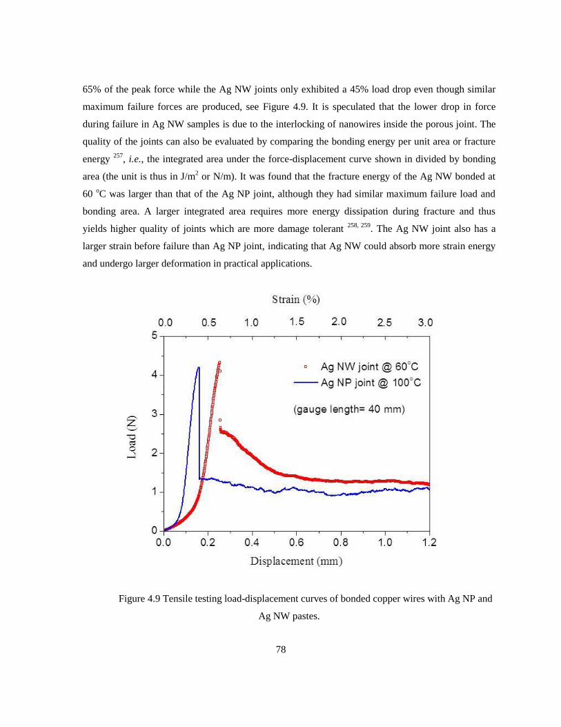
78
65% of the peak force while the Ag NW joints only exhibited a 45% load drop even though similar
maximum failure forces are produced, see Figure 4.9. It is speculated that the lower drop in force
during failure in Ag NW samples is due to the interlocking of nanowires inside the porous joint. The
quality of the joints can also be evaluated by comparing the bonding energy per unit area or fracture
energy 257
, i.e., the integrated area under the force-displacement curve shown in divided by bonding
area (the unit is thus in J/m2 or N/m). It was found that the fracture energy of the Ag NW bonded at
60 oC was larger than that of the Ag NP joint, although they had similar maximum failure load and
bonding area. A larger integrated area requires more energy dissipation during fracture and thus
yields higher quality of joints which are more damage tolerant 258, 259
. The Ag NW joint also has a
larger strain before failure than Ag NP joint, indicating that Ag NW could absorb more strain energy
and undergo larger deformation in practical applications.
Figure 4.9 Tensile testing load-displacement curves of bonded copper wires with Ag NP and
Ag NW pastes.
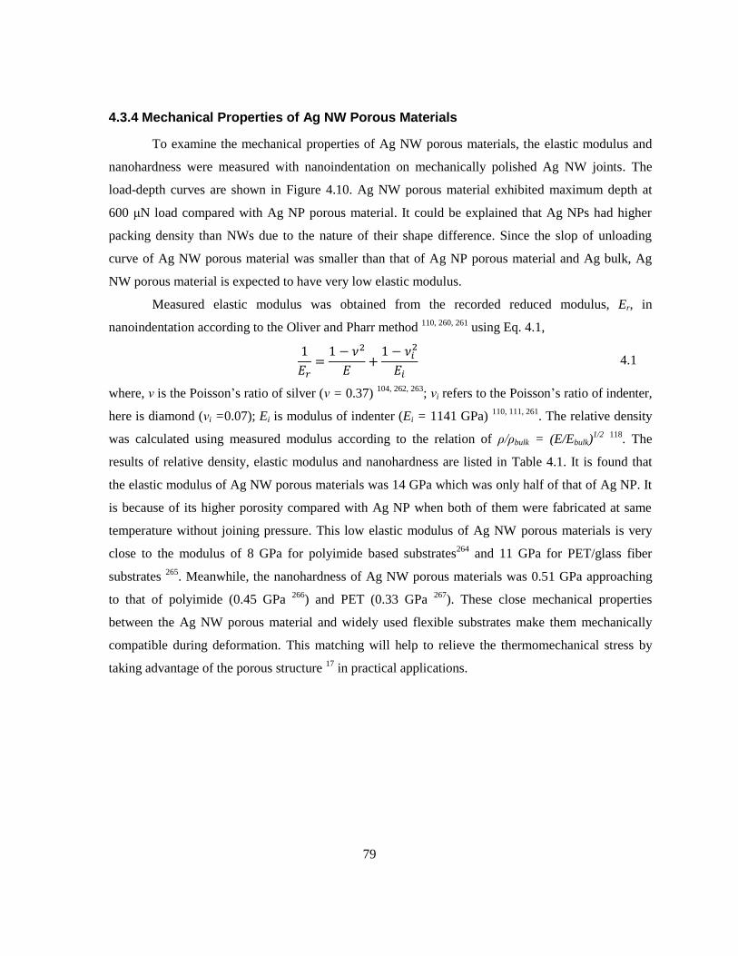
79
4.3.4 Mechanical Properties of Ag NW Porous Materials
To examine the mechanical properties of Ag NW porous materials, the elastic modulus and
nanohardness were measured with nanoindentation on mechanically polished Ag NW joints. The
load-depth curves are shown in Figure 4.10. Ag NW porous material exhibited maximum depth at
600 μN load compared with Ag NP porous material. It could be explained that Ag NPs had higher
packing density than NWs due to the nature of their shape difference. Since the slop of unloading
curve of Ag NW porous material was smaller than that of Ag NP porous material and Ag bulk, Ag
NW porous material is expected to have very low elastic modulus.
Measured elastic modulus was obtained from the recorded reduced modulus, Er, in
nanoindentation according to the Oliver and Pharr method 110, 260, 261
using Eq. 4.1,
4.1
where, ν is the Poisson‟s ratio of silver (ν = 0.37) 104, 262, 263
; νi refers to the Poisson‟s ratio of indenter,
here is diamond (νi =0.07); Ei is modulus of indenter (Ei = 1141 GPa) 110, 111, 261
. The relative density
was calculated using measured modulus according to the relation of ρ/ρbulk = (E/Ebulk)1/2
118
. The
results of relative density, elastic modulus and nanohardness are listed in Table 4.1. It is found that
the elastic modulus of Ag NW porous materials was 14 GPa which was only half of that of Ag NP. It
is because of its higher porosity compared with Ag NP when both of them were fabricated at same
temperature without joining pressure. This low elastic modulus of Ag NW porous materials is very
close to the modulus of 8 GPa for polyimide based substrates264
and 11 GPa for PET/glass fiber
substrates 265
. Meanwhile, the nanohardness of Ag NW porous materials was 0.51 GPa approaching
to that of polyimide (0.45 GPa 266
) and PET (0.33 GPa 267
). These close mechanical properties
between the Ag NW porous material and widely used flexible substrates make them mechanically
compatible during deformation. This matching will help to relieve the thermomechanical stress by
taking advantage of the porous structure 17
in practical applications.
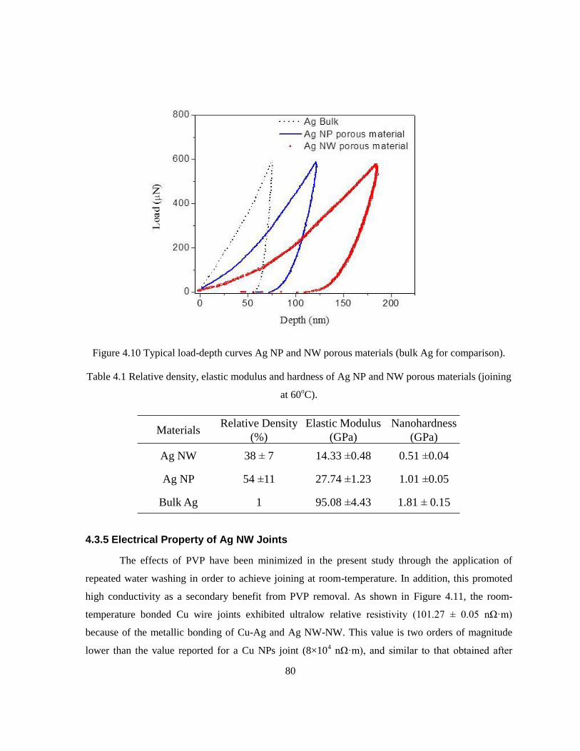
80
Figure 4.10 Typical load-depth curves Ag NP and NW porous materials (bulk Ag for comparison).
Table 4.1 Relative density, elastic modulus and hardness of Ag NP and NW porous materials (joining
at 60oC).
4.3.5 Electrical Property of Ag NW Joints
The effects of PVP have been minimized in the present study through the application of
repeated water washing in order to achieve joining at room-temperature. In addition, this promoted
high conductivity as a secondary benefit from PVP removal. As shown in Figure 4.11, the room-
temperature bonded Cu wire joints exhibited ultralow relative resistivity 101.27 ± 0.05 nΩ·m
because of the metallic bonding of Cu-Ag and Ag NW-NW. This value is two orders of magnitude
lower than the value reported for a Cu NPs joint (8×10⁴ nΩ·m , and similar to that obtained after
MaterialsRelative Density
(%)
Elastic Modulus
(GPa)
Nanohardness
(GPa)
Ag NW 38 ± 7 14.33 ±0.48 0.51 ±0.04
Ag NP 54 ±11 27.74 ±1.23 1.01 ±0.05
Bulk Ag 1 95.08 ±4.43 1.81 ± 0.15

81
prolonged times in cured and reflowed Ag nanocomposites 60 nΩ·m 18, 268
. The resistivity measured
here was the relative resistivity of Cu-Ag joint with the configuration shown in the inset image of
Figure 4.11.
For comparison, the resistivity of the Cu wire was plotted which presents a linear relationship
with temperature because of temperature coefficient of resistance 269
. This coefficient accounts for the
slightly increasing of resistivity of bonded joint from 18 oC to 150
oC. The further sintering of the Ag
NWs at elevated temperatures results in the enhancement of conductivity. At 250 oC, the joint
obtained the lowest resistivity 37.83 ± 0.04 nΩ·m which is comparable with 35.58 ± 0.12 nΩfflm
observed for a pure Cu wire. However, because of broken nanowires and oxidation of Cu after 250
oC, grown temperature introduced the increasing of resistivity.
Figure 4.11 Relative resistivity of bonded Cu wire joint with Ag NW paste washed three times as a
function of sintering and testing temperatures. Bulk resistivity of pure Cu wire was compared. Inset:
the configuration of measured joint, relative resistivity was calculated using ρ=RA/l with the
measured resistance (R), cross-section area of joint (A), and length for measuring voltage drop (l).

82
4.3.6 Microstructure Characterization
Two Cu wires can be identified with a 20 µm gap and the interface between Cu and Ag
matrix is very sharp in Figure 4.12a. The structure of filler material was less of micropores (Figure
4.12b) as in the case of Ag metallo-organic NPs joint 173
, however, the joint was nanoporous because
no pressure was applied during the joining process. In the interface as shown in Figure 4.12c, the
metallurgical bond between the Cu wire and the Ag paste was found to be continuous. The EDX line
scan shows the Ag and Cu elements could form a ~0.5 µm transition layer by diffusion.
Figure 4.12 Microstructures of cross sections of Ag NW paste bonded Cu-Cu joints at room
temperature: (a) Two Cu wires can be identified with a 20 µm gap filling with Ag NW paste with the
bonded wires shown in the inset; (b) Optical microscope image of clear interface of Cu and Ag
matrix; (c) SEM image of bonded interface of cross section shows the bond is continuous and formed
metallurgical bond between the Ag nanomaterials and Cu wire; Dashed arrow indicating (d) the EDX
line scanning direction, Ag and Cu elements formed a 0.5 µm transition layer by atoms diffusion.
The fracture surfaces of bonded samples before and after testing have been observed to
investigate the joining behavior of Ag NW pastes. At room-temperature, no testing sample depicts the
straight Ag NWs well interconnected and formed three-dimensional Ag discontinuous networks in
Figure 4.13a aforementioned. In TEM images Figure 4.13b, the Ag NWs are joined together in either
an end-to-end, end-to-side, or side-to-side manner. After testing, some interconnected Ag NWs were
broken as highlighted with circles in Figure 4.13c. The Ag NWs were distorted because of the strain
under loading which indicates the Ag NW discontinuous networks are good for absorbing mechanical

83
stress. This high strength of nanowires due to the nano-scale effects 102
and the good mechanical
property of discontinuous networks accounts for the fracture strength of joints. However, at high
joining temperature, Ag NWs transformed into particles and the failure points of filler materials were
difficult to identify (see Figure 4.13d).
Figure 4.13 SEM (a) and TEM (b) images of three-dimensional Ag discontinuous networks formed at
room-temperature. Arrows indicating the Ag-Ag junctions, numbers 1, 2 and 3 showing end-to-end,
end-to side and side-to-side three different joining modes of Ag NWs. Fracture surface of joints
formed at (c) room-temperature and (d) 300 oC. Circles indicated the failure of Ag NWs.
It is interesting to note that the Cu wire fracture surface of joint bonded at room-temperature
was covered by a residual thin layer of Ag NW after testing as shown in Figure 4.14a. This indicates
that the fracture of the joint is not in the interface of Cu-Ag, but rather the Ag NW discontinuous
networks close to the Cu interface. The high-magnification SEM images of Ag network matrix is
depicted in Figure 4.14b showing 100% pure Ag in EDX results. Some particles mixed with and grew
on Ag NWs which are in the folded thin layer in Figure 4.14c and on the Cu surface in Figure 4.14d.
This thin layer contains 18 at.% O and 20 at.% Cu (see Figure 4.14c) while the Cu surface is 23 at.%
O in Figure 4.14d. Therefore, the particles were CuO which originated from the oxidation of Cu on
the surface. Those CuO nanoparticles might be from the Cu surface because of incomplete cleaning
or oxidation of Cu during joining. However, those nanoparticles dramatically decreased on the Cu
surface when joining temperatures increased to 100 oC, see Figure 4.14e. If the joining temperatures

84
continue to increase to 150 oC, no CuO particles are observed obviously, but only well interconnected
and distorted Ag NWs appear on the Cu surface, see Figure 4.14f. In addition, the presence of CuO
might serve as a beneficial co-bonding material in local areas during the room-temperature joining
and contribute to the good mechanical properties of joints.
Here, one should consider that the bonds of the PVP could be terminated with hydroxyl
groups due to the presence of hydrogen peroxide and water in polymerization during fabrication
process 270
. Hence, PVP can be used as not only a stabilizer but also a reducing agent 271
as it has been
successfully used to synthesis noble metal nanomaterials 272-274
. It is believed that the residual PVP on
the surface of Ag NWs or in the water of paste could prevent the formation of CuO and/or deoxidize
CuO to Cu and further clean the Cu-Ag interface and provide better conditions for interdiffusion and
joining. This “in-situ cleaning” mechanism is proposed as follows: hydroxyl groups terminated PVP
reacts with copper oxide and generates copper in an “in-situ cleaning” process during joining, or
prevent the formation of copper oxide shown in Figure 4.15. This phenomenon will be discussed later
in detail.
Figure 4.14 SEM images of (a) failure joint bonded at room-temperature, the high-magnification
images of squares corresponding to (b) Ag matrix surface, (c) folded Ag NW layer, with particles
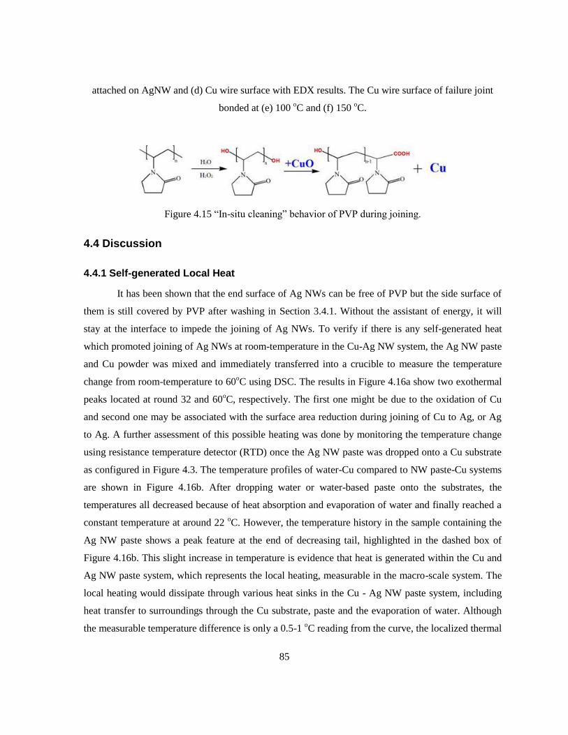
85
attached on AgNW and (d) Cu wire surface with EDX results. The Cu wire surface of failure joint
bonded at (e) 100 oC and (f) 150
oC.
Figure 4.15 “In-situ cleaning” behavior of PVP during joining.
4.4 Discussion
4.4.1 Self-generated Local Heat
It has been shown that the end surface of Ag NWs can be free of PVP but the side surface of
them is still covered by PVP after washing in Section 3.4.1. Without the assistant of energy, it will
stay at the interface to impede the joining of Ag NWs. To verify if there is any self-generated heat
which promoted joining of Ag NWs at room-temperature in the Cu-Ag NW system, the Ag NW paste
and Cu powder was mixed and immediately transferred into a crucible to measure the temperature
change from room-temperature to 60oC using DSC. The results in Figure 4.16a show two exothermal
peaks located at round 32 and 60oC, respectively. The first one might be due to the oxidation of Cu
and second one may be associated with the surface area reduction during joining of Cu to Ag, or Ag
to Ag. A further assessment of this possible heating was done by monitoring the temperature change
using resistance temperature detector (RTD) once the Ag NW paste was dropped onto a Cu substrate
as configured in Figure 4.3. The temperature profiles of water-Cu compared to NW paste-Cu systems
are shown in Figure 4.16b. After dropping water or water-based paste onto the substrates, the
temperatures all decreased because of heat absorption and evaporation of water and finally reached a
constant temperature at around 22 oC. However, the temperature history in the sample containing the
Ag NW paste shows a peak feature at the end of decreasing tail, highlighted in the dashed box of
Figure 4.16b. This slight increase in temperature is evidence that heat is generated within the Cu and
Ag NW paste system, which represents the local heating, measurable in the macro-scale system. The
local heating would dissipate through various heat sinks in the Cu - Ag NW paste system, including
heat transfer to surroundings through the Cu substrate, paste and the evaporation of water. Although
the measurable temperature difference is only a 0.5-1 oC reading from the curve, the localized thermal

86
energy per volume is likely to be much higher since it is generated at the nanosized interfaces and
transferred to macro components. The experiments demonstrated that this self-generated local heating
would be sufficient to promote joining of Ag NWs and Ag NWs to Cu substrates. However, it only
behaves as a slight temperature increase, and thus does not affect the heat sensitive substrate during
joining process, which makes it a very promising approach for room-temperature joining.
Figure 4.16 (a) DSC curve of Ag NW paste with Cu powder heating in air. (b) Temperature profiles
of pure water and Ag NW paste with Cu substrate.
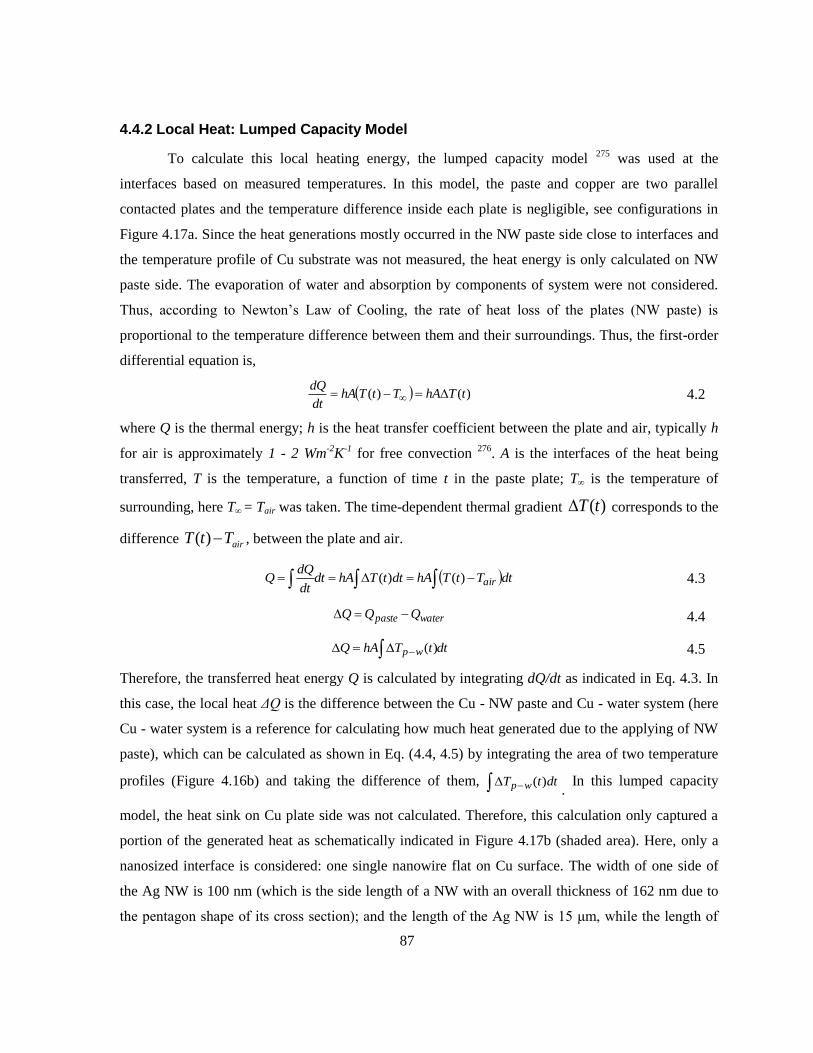
87
4.4.2 Local Heat: Lumped Capacity Model
To calculate this local heating energy, the lumped capacity model 275
was used at the
interfaces based on measured temperatures. In this model, the paste and copper are two parallel
contacted plates and the temperature difference inside each plate is negligible, see configurations in
Figure 4.17a. Since the heat generations mostly occurred in the NW paste side close to interfaces and
the temperature profile of Cu substrate was not measured, the heat energy is only calculated on NW
paste side. The evaporation of water and absorption by components of system were not considered.
Thus, according to Newton‟s Law of Cooling, the rate of heat loss of the plates NW paste is
proportional to the temperature difference between them and their surroundings. Thus, the first-order
differential equation is,
)()( tThATtThAdt
dQ 4.2
where Q is the thermal energy; h is the heat transfer coefficient between the plate and air, typically h
for air is approximately 1 - 2 Wm-2
K-1
for free convection 276
. A is the interfaces of the heat being
transferred, T is the temperature, a function of time t in the paste plate; T∞ is the temperature of
surrounding, here T∞ = Tair was taken. The time-dependent thermal gradient )(tT corresponds to the
difference airTtT )( , between the plate and air.
dtTtThAdttThAdtdt
dQQ air)()( 4.3
waterpaste QQQ
4.4
dttThAQ wp )(
4.5
Therefore, the transferred heat energy Q is calculated by integrating dQ/dt as indicated in Eq. 4.3. In
this case, the local heat ΔQ is the difference between the Cu - NW paste and Cu - water system (here
Cu - water system is a reference for calculating how much heat generated due to the applying of NW
paste), which can be calculated as shown in Eq. (4.4, 4.5) by integrating the area of two temperature
profiles (Figure 4.16b) and taking the difference of them, dttT wp )(.
In this lumped capacity
model, the heat sink on Cu plate side was not calculated. Therefore, this calculation only captured a
portion of the generated heat as schematically indicated in Figure 4.17b (shaded area). Here, only a
nanosized interface is considered: one single nanowire flat on Cu surface. The width of one side of
the Ag NW is 100 nm (which is the side length of a NW with an overall thickness of 162 nm due to
the pentagon shape of its cross section ; and the length of the Ag NW is 15 μm, while the length of

88
the Cu surface is 20 μm since the Cu surface was not fully covered as shown in Figure 4.17c. This
coverage value corresponds to 46% in this case, which is close to the range of 40-50% based on TEM
images. Therefore, A = 162 nm × 20 μm is the projection area of the single NW - Cu nano-interface
system on paste-air interface (based on the parallel plate assumption). The minimum heat transfer
coefficient of still air at room temperature was assumed to be 1 Wm-2
K-1
to calculate the minimum
transferred heat energy. The difference between the two curves is around 433 K∙s (from the peak
temperature after applying paste/water at 730 s to the stable temperatures at 1038 s). Then, the local
heat ΔQ will be 1.40 nJ (on the NW paste side for a thin slice with cross section area of A).
Figure 4.17 (a) Cu and NW paste plate assembly for heat energy calculation using lumped capacity
model and (b) its schematic of temperature profile with calculated localized heat energies at the
nanoscale. (c) Side view of localized interface with size configurations.

89
4.4.3 Interfacial Reaction
The cross-section shows that the Cu and Ag NW were in close contact on the round interface,
without obvious unbounded interfaces. Due to the nature of liquid in the Ag NW paste, it can flow
around the Cu wire and fill the gap between two components to make a complete connection around
the circumference. SEM analysis with an EDX line scan across the interface indicates only Cu and Ag
with undetectable oxygen (see Figure 4.12d). On the fracture surface, a thin Ag NW layer on Cu wire
surface was observed as shown in Figure 4.18a. The Ag NWs were interconnected at room-
temperature in the filler Ag NWs (Figure 4.18b) similar to the previous sintering results indicate in
Figure 4.6d. Meanwhile, many nanoparticles were clearly observed on the surface of Ag NW within
this thin layer (Figure 4.18c) close to the Ag-Cu interface. These nanoparticles show darker contrast
than Ag NWs if compared to the in-lens and backscattering images in Figure 4.18d, suggesting that
they contain lighter elements compared with Ag, in this case Cu. Figure 4.18e clearly illustrates the
nanoparticles grew on the surface of Ag NWs. According to XRD, EDX analysis via HRTEM, these
nanoparticles have been identified as CuO 277
. The difference in chemical potentials of Cu and Ag
implies that Cu would be oxidized to Cu ions and migrate to defect areas on the surface of the Ag
NWs, and combine with oxygen to grow Cu2O which later transforms to CuO.
According to the observation of the fracture surfaces of samples bonded at room-temperature
without further heat treatment and with heating at higher temperatures, the untreated sample
contained a high density of CuO nanoparticles on the surface of Ag NWs (shown in Figure 4.14d or
Figure 4.18c). However, CuO nanoparticles decreased significantly after heat treatment (see Figure
4.14e-f). After treating at 150oC, the present nanoparticles on the surface of Ag NWs can only be
observed under high magnified SEM image as illustrated in Figure 4.19. The morphology of them is
different with the observed CuO nanoparticles as noted in Figure 4.19b. It is confirmed that the
residual PVP served as reducing agent to react with CuO and obtain Cu nanomaterials as scheme
suggested in Figure 4.15. To reproduce this process, the CuO-Ag NW composite was heated in water
solutions containing PVP at a higher temperature of 80oC as studied by Xiong et al.
278. At room-
temperature, most of these CuO nanoparticles grown on the surface exhibit an amorphous structure
under TEM observation, see Figure 4.20a-b. After heating in PVP solution, the CuO nanoparticles
became much smaller and more agglomerations were observed in Figure 4.20c. HRTEM image
indicates that the amorphous structures decreased and more crystalline nanoparticles were observed
after reaction, see Figure 4.20d. Based on lattice diffraction and EDX results, most of the CuO
nanoparticles on the surface of the Ag NWs were found to have transformed to Cu nanocrystals. This

90
suggested that at higher temperatures PVP on Ag NW surfaces could clean the CuO formed during
the joining process at room-temperature. It can reduce or prevent the oxidation of Cu and Ag during
joining process because of self-generated local heating, demonstrating a “self-cleaning” mechanism
among Cu-PVPs-Ag system as previously discussed in Section 4.3.6.
Figure 4.18 SEM images of (a) fractured sample and (b) fractured surface on Ag NW side. (c)
Nanoparticle decorated Ag NW layer. (d) Comparison of InLens and Back-scatting images of NP
decorated NWs, indicating the NPs have different composites with Ag NWs. (e) TEM micrograph of
NP grow on the surface of Ag NW taken from Cu-Ag interface of bonded sample.

91
Figure 4.19 SEM micrographs of fractured interfaces of joint formed at room-temperature: (a) heated
at 150oC for 1 hr and its high resolution image (b).
Figure 4.20 SEM and TEM images of (a, b) CuO grown on the surface of Ag NW at room-
temperature with large portions of amorphous structures and (c, d) changing to Cu nanocrystalline
structures after heating at 80oC for 3 hrs.
4.4.4 Local Temperature
It is worth noting that the local heating may originate from the oxidation of copper and the
reaction of PVP on the Cu-Ag interfaces, the reduction of surface during joining of Ag-Ag or Cu-Ag
could contribute to the generation of heat as well. To understand mechanism of this self-generated

92
local heating induced nanojoining at the nanoscale, some simple calculations of the temperature rise
can be made base on the enthalpy of reactions. First, the oxidation of Cu will release heat ΔH1 as
shown in Eq. 4.6. Due to the long term oxidation of Cu during the joining time scale of a few seconds
to minutes, the heat energy is difficult to calculate because of a heat sink effect. However, this
reaction will produce CuO and supply the initial heat for CuO reacting with PVP, which could
generate heat ΔH2 (Eq. 4.7). Meanwhile, the removal of PVP at the interface and the generated heat
can promote the interdiffusion of Ag and Cu to form metallic bonds, see Figure 4.21a-b. This reaction
is shown in Eq.4.8 and ΔH3 is the released heat calculated according to reduced surfaces of Cu and
Ag because the composition of AgxCu and its reaction heat is difficult to be identified. Here, both of
the surfaces of Cu and Ag are considered and they are the (100) plane and surface energies of them
can be found in literature 279
. The heats from the enthalpy change of the first two reactions Eq. 4.6,
4.7 can be obtained from thermochemical data handbooks 280
. Since the thermodynamic data of PVP
is difficult to obtain, one can simplify the long chain R as methyl.
12 22 HCuOOCu 4.6
222 22 HOHCOOHRCuOHCHRCuO
4.7
3HCuAgCuxAg x
4.8
Due to a layer of CuO coated on Cu and Ag surface in the single NW-Cu localized system
and the CuO-PVP reaction mainly occurring on the Ag NW surface, the heat ΔH2 will directly
conduct to Ag NW to heat it up. It is difficult for this heat to transfer to the surrounding water / air
because of their small thermal conductivities, KH2O =0.58 W∙m-1
∙K-1
, Kair =0.024 W∙m-1
∙K-1 281
. The
presence of CuO at Cu-Ag interface (Figure 4.21a) will block the heat transfer from Ag to Cu
substrates since its thermal conductivity, KCuO = 20 W∙m-1
∙K-1
282
, which is 20 times smaller than that
of Ag, KAg =427 W∙m-1
∙K-1281
. If the CuO coated Ag NWs are away from Cu-Ag interface, the
surroundings water and air also act as a thermal barrier to keep the heat inside the Ag NWs.
Therefore, one can calculate the temperature raise of one single Ag NW as indicated in Eq.4.9:
AgAg
Agmc
HT 2
4.9
where c is the specific heat capacity of Ag (cAg= 0.240 J∙g-1
∙oC
-1)
283 and mAg stands for mass of Ag
NW. As mentioned previously in Section 4.4.1, one side of the Ag NW is 100 nm and length of Ag
NW is 15 μm (Figure 4.21), yielding mAg = 2.706×10⁻¹²
g. Here, It is assumed that the CuO layer with
10 nm thick and 100% coverage on Ag NW was completely reacted, and that, ΔH2 is 0.314 nJ. Since

93
ΔH1 and ΔH3 are excluded here, this local heat value is smaller than the calculated value of total local
heat ΔQ using lumped capacity model (Section 4.4.1). However, they are quite close. Considering the
single Ag NW, ΔTAg = 484 oC, finally (that is, temperature of Ag NW will be 504
oC when room
temperature is 20 oC). This high temperature is striking, however one should note that this calculation
is based on the assumptions of perfect surface area coverage of CuO, and that there is sufficient PVP
content in the paste to support the reaction. Furthermore, the CuO-PVP reaction in Eq. 4.7 was
assumed as a static process and would generate heat instantaneously. However, this reaction in reality
is a dynamic process with different rates of reaction depending on the concentration gradient of
chemicals, temperature, pressure and the use of catalyst. Since the complexity of reaction conditions
in this study, especially in the single Ag NW- Cu system as depicted in Figure 4.21, there is no data
of their reaction rate available in present literatures for such nano scale system and it is also too
difficult to be measured experimentally. Therefore, this calculated high temperature is a predicted
instant maximum value. In fact, the reaction would probably last for few minutes during joining
process, meaning that the heat was released gradually and accumulated in a local area because of low
thermal conductivities of surroundings. Considering the long-term time scale during the actual joining
process, the maximum local temperature of Ag NW would be lower than 504 oC because of the
limiting kinetics of the CuO-PVP reaction and heat sink effects. To generally predict the local
temperature of Ag NW in this study, both the heat generation from the reaction and heat transfer into
Ag NW are instantaneous as assumed previously. It suggests that the Ag NW is substantially heated
above room temperature after the CuO-PVP reaction, see Figure 4.21b. The reaction will consume the
residual PVP in the water of paste and on the surface of Ag NWs, leading the less PVP in the
interfaces and making the side surface of Ag NWs exposed and activated as well for joining similar as
the end surface activation in Chapter 3. Also, this temperature rise will trigger the nanojoining of Ag
NWs when they are in contact and induce a significant sintering of nanomaterials system 172, 284
to
form networks. It is also sufficient to supply the energy for Cu and Ag atomic diffusion at Ag NW-
Cu interface.

94
Figure 4.21 Schematic illustration of cross-section view of simplified Cu-Ag localized interface (a)
before and (b) after temperature rise due to CuO-PVP reaction.
It is worth noting that this temperature is supposed to be the transient maximum value of Ag
NW since the heat which would be conducted out was ignored and the reduction heat from Eq. 4.7 is
the maximum due to the 100 % coverage setup of CuO on Ag NW surface. Obviously, although this
calculated temperature is a preliminary estimate, it provides some insights as to how the local heating
effect contributes to joining, even though surrounding components remained near room-temperature.
The estimation shows that the negligible heat energy at bulk size cannot be ignored at a nanoscale. On
the contrary, if it can be manipulated well, such weak heat energy can be collected and adopted for
many new applications. It is also notable that the heat is self-generated and in-situ delivered to the
interfaces at a nanoscale where the interconnections are required.
The locally generated heat mainly from Cu-to-CuO-to-Cu cycle reactions would cause atom
diffusion at the Cu-Ag interfaces of Ag NWs and substrate joining. It also conducts throughout the
paste and promotes the joining of Ag NWs. The reduction of Ag NW surface energy due to Ag NW
joining could release energy and cause secondary local heating at Ag-Ag interface for atom
interdiffusion, suggesting it is also an acceleration factor to form three dimensional Ag NW networks
for interconnecting the substrates.
Another considerable effect playing positive role for joining of Ag NWs in the water-based
paste is the capillary force during water evaporation process. It could bring two or more NWs into
close contact with their neighboring NWs. At a nanoscale, this force can generate considerable
pressure at the interface of two NWs even it is fairly weak at micro scale. In terms of pressure here, it
comes from the internal system originating from the capillary force or surface tension of water rather
than the external pressure applying to the system to assist the joining process. Therefore, the self-

95
pressed process by solvent/water evaporation during joining is worth to be noted here. However, only
local heating effects have been comprehensively studied in this study.
4.4.5 Local Heating Effects Induced Nanojoining
Beside of the elevated local temperature can accelerate diffusion for joining, one can expect
that the reduction of organics in the pastes will also have its contribution. As suggested above, the
local heating is partially from the CuO-PVP reaction by consuming the residual PVP in the water of
paste to further reduce the organic content in the paste. It also consumes the PVP protection layer on
the side surface of Ag NWs to activate the side surfaces. These all can reduce the organics to provide
cleaner interfaces of Ag NW-NW and Ag NW-Cu for joining. Further, the local heating can also
break down the unreacted PVP on the surfaces of Ag NWs to activate more clean sites for joining.
To examine if these local heating effects are sufficient to induce atomic diffusion and
metallic bond formation, the interfaces of Cu-Ag and Ag-Ag were characterized using HRTEM.
Figure 4.22a shows the porous structure of the interface of Cu and Ag, formed by the room-
temperature pressureless joining process. The interfacial regions where the Cu surface was bonded
with Ag, and Ag to Ag NW bonds formed are indicated by arrows in Figure 4.22a. The HRTEM
image indicates that the Cu and Ag NW were metallurgically bonded, with the (100) plane of Ag and
(111) of Cu connected in Figure 4.22b. Ag NW bonded on Cu surface and the (111) plane of Ag and
(200) of Cu well matched and formed metallic bond as well, see Figure 4.22c-d, similar to that
observed when using Ag nanoparticle paste as the filler material 16, 172, 173
and connected with CuO
particles.
Figure 4.23a depicts the end-to-end joining of Ag NWs and the square area corresponding to
Figure 4.23b. The distances of lattice fringes are 2.32 Å and 1.96 Å in agreement with (111) and
(200) planes of silver 285, 286
. Ag NWs were interconnected via end-to-side or side-to-side manner and
formed metallurgical bonds as well, and Figure 4.23c illustrates a tri-junction of these Ag NWs.
Usually, the tips of Ag NWs have a thinner layer of PVP organics 287
which could more readily join
with others because of a smaller barrier gap and higher surface energy for atomic diffusion. Although
the washing process can remove or break the thin layer of PVP on the ends of Ag NWs to make it
activated for joining, the side surfaces of Ag NWs are difficult to active as discussed in previous
Chapter 3. Here, with the help of local heating effect, the sides of Ag NWs also started to connect
under room temperature joining process as shown in the inset image of Figure 4.23d, where (200) and
(220) lattices were continuous. Therefore, the local heating could break down the localized organic

96
layer on the side surface of the Ag NWs and promote the interdiffusion of atoms and form the joints
at even room-temperature when a Cu substrate is present. The clear metallic bonding at the atomic
level accounts for the good bond strength and conductivity observed during testing.
Figure 4.22 TEM images of (a) nanoporous Cu-Ag interface (arrows indicating the joining of Ag-Cu
and Ag-Ag), (b) lattice image of Cu (111) -Ag (100) interface; (c) Cu-Ag interface and corresponding
high-resolution image (b): lattice fringes showing the (111) plane of Ag and (200) of Cu well
matched. Arrows indicating the lattice directions of polycrystalline Cu.

97
Figure 4.23 TEM images of the interface of two AgNWs of joint bonded at room-temperature (a) with
end-to-end joining and square area corresponding to the high-resolution image (b); (c) tri-junction of
Ag NWs and (d) lattice image of side-to-side Ag-Ag interface.
4.5 Summary and Remarks
In summary, this chapter considered the feasibility of room-temperature pressure-free joining
of copper wires using water-based silver nanowire paste. A novel mechanism of self-generated local
heating within the silver nanowire paste and copper substrate system promoted the joining of silver-
to-silver and silver-to-copper without any external energy input. The CuO-PVP reaction could
consume the residual PVP on the side surface of Ag NWs and in the water of paste to further reduce
the organic content in the washed paste. The localized heat energy has been delivered in-situ to the
interfaces and promoted atomic diffusion and metallic bond formation with the bulk component
temperature stays near room-temperature. This local heating effect has been detected experimentally
and confirmed by calculation. The use of chemically generated local heating would be an alternative
method for energy in-situ delivery at micro/nanoscale.

98
This chapter has also shown that three-dimensional silver networks exhibit good conductivity
and strength for flexible electronics packaging. Due to the porous structure, Ag NW joints have lower
modulus in close to that of flexible substrates. Low modulus makes it more compatible with flexible
substrates and has more capacity to absorb mechanical stresses under strain. Consequently, next
chapter will focus on the mechanical properties of Ag NWs reinforced NP joints. In Particular, the
improvement of strength and the mechanical behaviors of silver nanowires in NP matrix under
loading will be studied.

99
Chapter 5
Reinforcement of Silver Nanoparticle Joints with Nanowires‡
5.1 Introduction
The use of lead alloy solder materials in the electronics industry has raised much concern due
to health, environmental and safety issues worldwide 130-133
. With the development of
nanotechnology, environmentally-friendly and flexible electronic products are becoming more
feasible in the near term 8, 11, 135, 248, 288
. The use of metallic nanoparticles (NPs) combined with ink-jet
printing processing for flexible electronics manufacturing, is a well-known technique in which the
deposition and patterning are simultaneously accomplished by printing a solution of the active
materials (e.g. Metallic NPs or conductive polymers), and has been widely studied 289-292
. The
material deposited using an ink-jet typically consists of gold or silver NPs encapsulated within
protective shells and dispersed in a liquid solvent 293, 294
. Recently, nanoscale diffusion bonding using
metallic nanomaterials has displayed significant advantages over conventional soldering or adhesive
bonding, such as lower bonding temperatures and higher diffusion rate 13
. Hence, low temperature
interconnection processes using metallic NP paste appears to be a promising alternative for Pb-free
electronic packaging and flexible electronic interconnections 172, 295
. For example, several studies have
focused on low temperature joining technology for lead-free packaging or power modules using NPs
made from silver 173, 296
, copper 297
and gold 19
, respectively. The sintering of silver NPs and their
bonding to copper wires and substrates to form a 3-dimensional bonded network which can withstand
higher working temperatures through further sintering has been reported by Hu et al. 172
and Alarifi et
al. 16
. The typical sintering temperature ranges from 150 ~ 300°C are lower than the melting point of
the corresponding bulk materials, due to the size effect of NPs 71
. However, pressure is required to
facilitate the bonding processing in these studies, which is still inconvenient for industrial
applications.
Recently, there is increasing interest in applications of one dimensional micro-sized / nano-
sized materials, for example, developing multifunctional composite materials incorporating second
phase fibers and/or whiskers 298-304
. Mullite fibers were added in carbon materials, which fibers bend
and fracture to several fragments that could partially carry the applied loading 305
. For a solder
ffi Portions of this study also appear in: Peng, P., et al., Reinforcement of Ag nanoparticle paste with nanowires
for low temperature pressureless bonding. Journal of Materials Science, 2012. 47(19): p. 6801-6811.

100
material, Coughlin et al. reported that Ni-Ti shape memory alloy fibers embedded into a Sn rich
solder alloy could improve fatigue and mechanical shock properties of the materials by a super-
elasticity transformation property of the fibers on loading 306
. Ongoing efforts are being made to study
the sintering of nanowires, nanorods and nanobelts, in order to further exploit the unique properties of
these materials 307-311
. However, few have examined the behavior of metallic joints when nanowires
are introduced as a second phase in the bonding material.
This section will focus on a low temperature pressureless joining process for robust wire to
wire bonding of copper by introducing silver nanowires (Ag NW) into a silver nanoparticle (Ag NP)
paste as filler materials. The sintering behaviors of Ag NP/NW binary pastes and mechanical
properties of bonded joints, furthermore, the reinforcement effect of Ag NW in the joints will be
discussed.
5.2 Experimental
5.2.1 Synthesis of Ag NPs and NWs
All the chemicals and reagents were of analytical grade and used in the as received form
without any purification. The synthesis of the Ag NP material involved reacting silver nitrate
(AgNO3, Alfa Aesar) and sodium citrate (C6H5O7Na3·2H2O, Alfa Aesar) at 80~90oC
16. Ag NWs
were prepared in a polyol solution with polyvinylpyrrolidone (PVP) as a structure directing reagent
using a method modified from the literature 66, 67
. In this study, 330 mg polyvinylpyrrolidone or PVP
((C6H9NO)n, K25, M.W.= 24000, Alfa Aesar) and 12.5 mg silver chloride (AgCl, Alfa Aesar) were
mixed with 40 ml ethylene glycol (EG, Fisher Chemical) in a round-bottom flask. The mixture was
heated to between 160 and170 oC. Then, 110 mg silver nitrate was dissolved in 10 ml ethylene glycol
liquid and added into the mixed solution while stirring vigorously and continuing the reaction
conditions for 4 hours. The Ag NPs and Ag NWs were condensed by centrifugation at 4000 rpm
using a 50 ml centrifuge pipe. The clean supernatants were removed from the centrifuge pipes using a
pipette resulting in highly concentrated Ag NP and Ag NW pastes. The excess PVPs in Ag NWs
could be washed and removed by deionized (DI) water and repeated centrifugation. 0%, 10%, 20%
and 30% volume fractions of Ag NW paste were mixed with Ag NP paste in 20 ml glass vials by
stirring and are designated as AgNP, AgNP/10NW, AgNP/20NW and AgNP/30NW, respectively.

101
5.2.2 Joining using Ag NP-NW Binary Pastes
The copper wires (99.9 % purity) used in this work, from Arcor Electronics, Northbrook, IL,
were 250 µm in diameter. Prior to bonding, the wires were cut into 60 mm pieces and ultrasonically
cleaned in acetone for 3 minutes to remove the organics, 1% diluted AgNO3 for 1 minute to remove
the oxide layer and rinsed in ultrapure water electrical resistivity approximately 18 MΩ·cm . A fine
needle attached on a 10 ml syringe was used to place the Ag nanopaste between two clean copper
wires on a 60 o
C hotplate surface. After depositing 0.05 ml Ag nanopaste, the assembly of copper
wires and paste was heated at 60~200 oC in air for 1 hour without bonding pressure.
5.2.3 Tensile Testing
Tensile shear testing was conducted by loading the wires in the axial direction at a rate of 0.5
mm/min using a micro tensile tester (Instron 5548, UK). Figure 5.1 illustrates the schematic diagram
of the tensile shear test samples used to investigate the mechanical performance of the bonded
samples. After clamping each bonded sample into the grips as shown in Figure 5.1, loading was
applied. The measured strength of joints is the tensile shear strength due to the applied shear stress
during the tensile testing, because two Cu wires were not coaxial. It was estimated by dividing the
highest failure force value by the bonding area 297, 312, 313
σ = Fmax/A (N/mm2 or MPa). The fracture
area of samples was difficult to measure due to the unsymmetrical geometry of fracture region. Here,
the average bonding area was estimated to normalize the actual fracture area, which bonding area A
was calculated by multiplying the maximum bonding length L by thickness D of the Ag bonding
material.
Figure 5.1 Schematic illustration of tensile shear strength testing of bonded samples. The starting
distance between the grips was fixed at 40 mm, L and D denote the bonding length and thickness of
joint.
102
5.2.4 Nanoindentation
The mechanical properties of silver npm were tested with a depth-sensing nanoindenter
(Hysitron Triboindenter) equipped with a Berkovich tip. The tip was calibrated on fused silica.
Indentations were performed on the mechanically polished flat surfaces in a load controlled mode. All
nanoindentation experiments were performed using a constant loading rate of 60 μN/s, with loads of
600 μN. A minimum of 5 indents for each load were collected for each sample.
5.2.5 Microstructure Characterization
The cross sections of bonded samples were mounted using epoxy resin and polished with 1
µm Al2O3 powder. Optical microscopy (Olympus BX 51M, Japan) and field-emission scanning
electron microscope (Leo 1530 FE-SEM; Zeiss, Germany) were used to study the microstructure of
cross sections, interfaces and fracture surfaces of bonded samples. Energy-dispersive X-ray
spectroscopy (EDX, EDAX Pegasus 1200) was employed for elemental analysis. The sintered Ag
NPs and Ag NP/NW were also observed using SEM.
5.3 Results
5.3.1 Microstructures of Sintered Ag NPs and Ag NWs
Figure 5.2 shows the microstructures of Ag NP and Ag NW pastes after centrifuging. Figure
5.2 a and b are low magnification SEM images of as-centrifuged Ag NP and Ag NW pastes. The Ag
NPs were 50 to 100 nm in size, with polyhedron morphology as shown in Figure 5.2c. The Ag NWs
had a pentagonal shape as shown in Figure 5.2d with lengths of 8 to 15 µm and 50 to 100 nm in
thickness. Few Ag NPs were also observed in the Ag NW paste synthesized by the polyol method.

103
Figure 5.2 Microstructure of condensed (a) AgNP and (b) AgNW paste after centrifuging. High
magnification SEM images of (c) polyhedron shaped Ag NPs and (d) pentagon shaped Ag NWs with
length of 10-20 µm and 50-100 nm thickness.
The Ag NP/NW pastes were sintered at different temperatures to investigate the sintering
behaviours of these mixtures at low temperature as shown in Figure 5.3. For comparison, unsintered
Ag NP/20NW binary paste is shown in Figure 5.3a. The microstructures of Ag NP/20NW binary
pastes sintered at 60 oC, 100
oC, 150
oC and 200
oC for 1 hour, respectively are shown in Figure 5.3b-
e. The average width of bridge paths between adjacent Ag NP-NP and Ag NP-NW grew from 26±2 to
54±4 nm (average of five measured values) as temperature increasing from 60 to 200 oC as indicated
by the arrows in Fig. 2b and 2e; which is consistent with the increased rate of solid state diffusion and
growth of bridge paths expected when the temperature increases. It is worth mentioning that residual
PVP from the synthesis process of the Ag NWs, and amorphous citrate complexes from the synthesis
process of Ag NPs could be present at the interfaces of the particles and influence the sintering of the
paste. Although PVP does not readily decompose below 300 o
C 216, 217
, the majority of this material

104
would be removed during the process of washing with DI water as previously shown when the PVP
coating was washed from Cu NPs 297
. As such, it would be expected that the particle surface free of
PVP is active for low temperature sintering. The amorphous citrate complexes on the surfaces of the
Ag NPs will readily vaporize and decompose (at temperatures above 90 oC) and should completely
disappear during low temperature sintering 172, 314, 315
. This accounts for the rapid formation and
growth of bridges even at temperatures of 100 to 150
oC. Sintered Ag NP/NW mixed pastes with
various additions of Ag NWs at 150 oC are also shown in Figure 5.3f, g, i, corresponding to 0%, 10%
and 30% Ag NWs by volume in the pastes (20% is shown in Figure 5.3d). Based on the dispersion of
the Ag NWs, it is clear they did not aggregate together and were uniformly dispersed in the Ag NP
paste by stirring. The inset images of Figure 5.3g and 2i illustrate the morphology of 10% Ag NW
and 30% Ag NW at a low magnification. Introducing a large fraction of Ag NWs can change the
packing of the nanomaterials in joints since spherical particles can be packed more densely than long
wires. This leads to the presence of a higher degree of porosity in the sintered 30% NW paste as
shown in the inset Figure 5.3j, compared with the paste containing 10% Ag NW(see Figure 5.3h).

105
Figure 5.3 SEM images of Ag NP/NW paste sintered at different temperatures: (a) unsintered Ag
NP/20NW paste, and sintered Ag NP/20NW paste at (b) 60 oC, (c) 100
oC, (d) 150
oC and (e) 200
oC
for 1 hour with arrows highlighting the bridge paths between NP-NP and NP-NW. Sintered paste with
different Ag NW volume additions (f) 0 vol.%, (g) 10 vol.% and (i) 30 vol.% after sintering at 150 oC
for 1 hour. Inset low magnification image (h) and (j) are corresponding to Ag NP/10NW and Ag
NP/30NW pastes.
106
5.3.2 Mechanical Properties
Two predominant fracture modes were observed during testing, one being filler material
fracture (failure of the sintered AgNP/NW) as shown in Figure 5.4a, and the other was interfacial
fracture at the Cu-Ag interface with one wire being pulled out of the sintered Ag bond material under
loading, as shown in Figure 5.4b. The fracture modes of all test samples bonded at different
temperatures are summarized in Table 5.1. Filler material fracture was usually observed when 0% and
30% Ag NW was introduced. The samples tested using Ag NP paste with 10 or 20% NW all involved
failure by interfacial debonding. In addition to these failure modes, fracture of the Cu wire occurred
in the sample bonded using Ag NP/20NW paste which was sintered at 200 oC.
Figure 5.4 During testing, two fracture modes for various NW contents: (a) filler material fracture and
(b) interfacial fracture on the Cu wire and Ag nanopaste joint interface.
Table 5.1 The fracture modes for bonded joints with various AgNW contents at different
temperatures.
Temperature Ag NP Ag NP/10NW Ag NP/20NW Ag NP/30NW
60 F*
I I F
100 F, I I I F, I
150 F I I F
200 F, I I I, W F
(* F, I and W denote the filler material fracture, interfacial fracture and wire fracture.)
The strength of bonded samples as a function of Ag NW volume fraction in the silver paste at
different bonding temperatures is presented in Figure 5.5a. The remarkable improvement in joint
tensile shear strength is suggested to be the result of reinforcement provided by the Ag NWs when
100 and 150 o
C sintering temperatures are used. The addition of 10 or 20% volume fraction of Ag
NW to the Ag NP paste increased the joint strength by 18 to 81% when the same sintering
temperatures are applied. However, the strength decreased considerably when 30% Ag NWs were

107
used due to the porous structure produced in the joint, as shown in Figure 5.3j. The highest strength
increase was obtained using 20% Ag NWs by volume, providing an improvement of 50 to 80% after
sintering at 60 and 100 oC bonding temperatures. Figure 5.5b shows the strength of bonded joints
with AgNP/20NW binary pastes and Ag NP paste as a function of bonding temperature. The presence
of 20% NW in the bonded joints clearly increased the failure strength compared to those without Ag
NW addition at all bonding temperatures investigated. For comparison, the Cu wires were also joined
by soldering (using commercial 60Sn-40Pb solder) at 200 o
C, and this joint achieved a strength of
9.9±0.4 MPa compared to 16.4±0.4 MPa and 13.9±0.5 MPa achieved using AgNP/20NW binary
pastes and Ag NP paste respectively. Prior studies investigating bonding with other paste materials
have also reported lower strengths when using Cu NPs (10 MPa) 297
or Ag NPs (8 MPa) applied with
5 MPa pressure 172
. A mean tensile shear strength of 3.2±0.8 MPa was obtained near room-
temperature (60 o
C) using Ag NP/20NW binary pastes. The incorporation of 10 to 20% Ag NWs
improved the strength of joints and shifted the failure area to the Cu-Ag interface instead of within the
sintered silver, due to the reinforcement of the sintered material by the nanowires.

108
Figure 5.5 (a) Bond strength of bonded samples as a function of Ag NW volume fraction at different
bonding temperatures. Squares, circles, triangles and diamonds represent tested samples bonded at
60oC, 100
oC, 150
oC and 200
oC, respectively. Open and closed symbols, representing the filler
material fracture and interfacial fracture, indicate the dominated fracture mode of bonded samples
with various Ag NW contents. The dashed line denotes the fracture strength of copper wires. (b) The
fracture strength of bonded samples of Ag NP/20NW and Ag NP pastes as a function of joining
temperature. Star represents 60%Tin/40%lead commercial solder joint soldered at 200oC.

109
The elastic modulus and nanohardness of these porous materials were characterized by
nanoindentation on mechanically polished Ag NP-NW joints. The typical load-depth curves are
shown in Figure 5.6. The maximum depth increased with increasing of Ag NW fraction because high
porosity was induced by adding more NWs. The relative density, elastic modulus and nanohardness
decreased with increasing of Ag NW fraction, see Table 5.2. The reduced elastic modulus and
nanohardness of Ag NP-NW porous materials suggests a good mechanical compatibility with flexible
substrates, which would aid in relieving the thermomechanical stress during practical applications (as
previously discussed in Section 4.3.4).
Figure 5.6 Typical load-depth curves of Ag NP-NW porous materials with different NW fractions.

110
Table 5.2 Relative density, elastic modulus and nanohardness of Ag NP-NW porous materials
(joining at 60oC).
5.3.3 Fracture Behaviours of Joints
To investigate the fracture mechanism of the sintered Ag NP/NW material, the fracture
surfaces were examined by SEM. Figure 5.7a-d show the SEM images of the secondary cracks
produced perpendicular to the fracture surfaces in joints bonded at 150 o
C with Ag NW volume
fractions from 0% to 30%. The regions reveal the role of the NW in the fracture of the bonding
material, since the primary crack cannot be readily characterized after failure. With the volume
fraction of Ag NWs increasing from 10% to 30%, progressively more crack bridging by the
nanowires occurs. Crack propagation is suppressed by bridging of the nanowires, in a similar way to
fibre reinforced composites 305
. Since each Ag NW was bonded with several Ag NPs, this reduced the
tendency for pull out of the NW. Clear evidence of plastic deformation of individual Ag NW was
observed as shown in Figure 5.7c. The fractured joints with 30% Ag NW addition exhibited a much
lower density of particles than those with 10 to 20% Ag NW addition, due to the highly porous
sintered structure discussed earlier (see Figure 5.3 h&j). This accounts for the dramatically decreased
bond strength when a 30% Ag NW volume fraction was used (see Figure 5.5a), which also hampered
the sintering process at lower temperatures. Moreover, the weaker bond strength between Cu wire and
Ag NW compared to Cu and Ag NP is likely attributed to the lower interfacial bonded area resulting
from the high porosity.

111
Figure 5.7 Microstructure of fracture Ag surface of NW reinforced Ag NP joints bonded at 150
with various Ag NW contents from (a) 0 vol.%, (b) 10 vol.%, (c) 20 vol.% to (d) 30 vol.%. Cracks are
indicated by dashed lines.
The cross-sections of fractured joints bonded with Ag NP/20NW paste are shown in Figure
5.8. Figure 5.8 (a-c) are taken by optical microscopy while Figure 5.8 (d-f) are SEM images of the
bonded interface. In Figure 5.8a, pull-out of the Cu wire is clearly identified by the dashed circle
indicating the original location of the second Cu wire. Some residual Ag can be observed on the
surface of the Cu wire after testing as indicated in Figure 5.8b. The bond interface of Cu-Ag is clearly
shown in Figure 5.8c and the pores observed may be due to a locally unbonded area resulting from air
bubbles introduced in the paste during bonding or an oxide layer on the Cu surface. A joint cross
section free of microporosity using Ag NP/20NW binary pastes was observed, see Figure 5.8d,
similar to the pressure bonded joints using Ag NPs 16, 180
. However, the presence of nanopores is
general in the joint with low temperature pressureless bonding. In the interface as shown in Figure
5.8e, the metallurgical bond between the Cu wire and the Ag paste was found to be continuous. The
backscattered electron SEM image Figure 5.8f indicates continuity along the Cu / Ag interface. A

112
region below the dashed line with 1 µm in thickness which is actually raised from the surface
considering the scratches on the surface formed during the polishing process. This surface relief is
common in metallographic samples where a phase is slightly harder, such as an intermetallic
compounded, and is not removed as much as the softer Ag or Cu. It is believed that the interdiffusion
of Ag and Cu atoms occur along the interface formed a mixed region or interphase boundary layer at
the interface 259
.
Figure 5.8 Microstructures of cross sections of AgNP/20NW paste bonded Cu-Cu joints: The pulled
out Cu wire can be identified by dashed line in an optical microscope image (a). (b) Ag matrix
attached on the surface of bare Cu wire and (c) bonded interface of Cu-Ag with pore highlighted by
arrow. Right column: (d) SEM image of bonded interface of cross section; (e) High magnification of
interface shows lack of gap or debonding area between the Ag sintered nanomaterials and Cu wire; (f)
The backscattered electronic SEM image for the interface, dark area denoting the Cu and bright area
for Ag.

113
To further study the Cu-Ag interface characteristics, the fractured joints bonded with Ag
NP/20NW binary pastes were investigated by SEM and EDX. Figure 5.9a was taken from the
fractured interface on Ag filler material side (as schematic illustrated in Figure 5.4b) and Figure 5.9b
was from the surface of pulled-out Cu wire with residual Ag NPs and Ag NWs. Three different spots
with different microstructures on both sides were studied using EDX. The results shown in Table 5.3
indicated that Cu and Ag elements existed on both sides, which supports the notion that interdiffusion
occurred and metallic bonding is present at the Ag and Cu interface during low temperature
pressureless sintering, similar to previous findings 172
.
Figure 5.9 SEM images of Cu-Ag interface: (a) AgNP/20NW paste side with labelled 1, 2, 3 three
points of interest, (b) Cu wire side with 4, 5, 6 points of interest, dotted line with arrows indicating
the Cu wire.
114
Table 5.3 EDX results of selected points on two different sides of the interface of a joint bonded with
AgNP/20NW paste at 150 oC
Interface Numbers O (At%) Cu (At%) Ag (At%)
Ag side
1 11 6 83
2 -- 34 66
3 15 66 19
Cu side
4 -- 7 93
5 -- 98 2
6 -- 78 22
5.4 Discussion
5.4.1 Fracture Energy
The load-displacement curves of bonded samples using Ag NP and Ag NP/NW also reveal
some key aspects which control the bonding strength. Typically, the load-displacement curves of the
joints produced using Ag NP/10NW paste developed a stepwise profile, and were distinct from that of
Ag NP paste bonded joints even though similar maximum failure forces are produced, see Figure
5.10. It is speculated that the stepwise failure is due to the integrative effects of debonding on Ag NP-
NP, NW-NP and NW-NW interfaces, and breaking of the Ag NWs. The quality of the joints can also
be evaluated by comparing the bonding energy per unit area or fracture energy 257
, i.e., the integrated
area under the force-displacement curve shown in Figure 5.10 divided by bonding area (the unit is
thus in J/m2 or N/m). It was found that the fracture energy of the Ag NP/10NW bonded at 60
oC was
about three times larger than that of the Ag NP joint, although they had similar maximum failure load
and bonding area. A larger integrated area requires more energy dissipation during fracture and thus
yields higher quality of joints which are more damage tolerant 258, 259
.

115
Figure 5.10 Typical load-displacement curves of bonded joints: solid line for AgNP/10NW and
dashed line for Ag NP.
5.4.2 Reinforcement Mechanisms
To study the behaviour of Ag NWs in joints bonded with Ag NP/NW pastes, the fracture
surfaces of tested joints were characterized by SEM. Four different morphologies of Ag NWs were
identified on the fracture surfaces and crack areas in Figure 5.11. The Ag NWs can be bent (Figure
5.11a) and pulled out (Figure 5.11b). In Figure 5.11b, some residual nanoparticles highlighted by
arrows attached to the end of a pulled-out Ag NW indicate that the debonding of Ag NP-NW actually
occurs within the paste matrix. This demonstrates that the Ag NP and Ag NW bonding strength is
relatively weak. Morphological features found on the fracture surface included necking of the Ag
NWs as highlighted by the arrows in Figure 5.11c and even breaking as shown in the circles of Figure
5.11d. These phenomena are all likely to occur simultaneously due to the wide range of stress
distributions in the NW which are randomly oriented. In Figure 5.11e a pair of bent and fractured Ag
NW fragments is evident, and even bending and plastic deformation zones in a NW are observed in
Figure 5.11f, with the necked regions highlighted by arrows. Due to the nano-scale effects, one would
expect that the wires should have extremely high strength, and that little plastic deformation will
occur since the slip process will be limited 102
. Overall, a rather small area reduction was observed at

116
the NW fracture surfaces, and this appears consistent with numerical modelling of 20 nm thick NW
also suggests that fracture will be rather brittle when their length is over 1.5 µm 316
. Nevertheless, the
NW second phase has a high strength, and is crucial for reinforcement in these bonded joints.
Figure 5.11 SEM images of silver nanowires in joints after testing: (a) NW bent under stress with
arrow indicating the bend region; (b) NW pullout, arrows highlighting residual NPs attached on the
top and wall of NW; (c) Plastic deformation of NW with deformation regions highlighted by arrows;
(d) NWs broken under stress, deformation region in the NW is shown. Not individually, the combined
actions of Ag NWs are illustrated: (e) Bent NW was broken into two wires under stress, the fracture
areas stayed in the circle; (f) NW was bent and pulled out, plastic deformation zones are highlighted
by arrows. Dashed lines indicate the cracks.
In comparison, the 0% NW sample exhibited fracture surface dominated by NP with few
bonded points, and so the above noted behaviours of Ag NWs were not available to dissipate the

117
fracture energy during loading, leading to inferior strength and toughness. A schematic representation
of the mechanisms occurring during fracture is illustrated in Figure 5.12 which summarizes the
reinforcement mechanisms provided by NWs in the bonded joints. In Figure 5.12a, the inter-particle
forces cause crack blunting by NP-NP debonding and crack widening if the stress on at the crack tip
is larger than the NP-NP debonding force 317, 318
. While the crack grows in the vicinity of NWs, the
crack-opening stress could be released along the NW and form a local compressive stress which
bends the NW as shown in Figure 5.12b. The strain and energy required for bending of a NW will
suppress the propagation of cracks or cause the crack deflection effectively reinforcing the joint 319,
320. If the bonding strength of NP-NW is larger than the yield strength of NW, then deformation or
even breakage of the NW could occur under loading (Figure 5.12c). In the case that bonding with the
NP matrix is poor around a NW, it could also be pulled out by the debonding of NP-NW and NP-NP
interfaces in Figure 5.12d. After an NW has been pulled out, a new smaller crack is easily to be
generated and propagated along the debonding plane. Both crack closure and creation will dissipate
the external fracture energy and thereby improve the strength of joint 321-323
.

118
Figure 5.12. Schematic mechanisms of AgNWs reinforcement in AgNP/NW joints: (a) Energy
absorption causing crack closure by NP-NP debonding and crack propagation. (NP-NP bond < stress
on crack tip); (b) While the crack grows in front of AgNW, the deformation splits along the NW and
forms a compressive stress then bends the NW. The dispersed strain and energy consumption of
bending NW stops the crack propagation or causes crack deflection. (Stress on crack tip < NW yield
strength < NP-NW bond); (c) Deformation or even breaking of NW. (NW yield strength < Stress on
crack tip < NP-NW bond); (d) NW being pulled out by debonding of NP-NW and further diversion of
the crack. (NP-NW bond < Stress on crack tip). New generated smaller crack can propagate in the
debonded areas.
5.5 Summary and Remarks
In summary, a unique method for interconnecting of copper wires using silver nanoparticle
and nanowire binary pastes has been examined in this chapter, in which joining was accomplished
from 60 to 200 oC and yet without the application of pressure. Joining was facilitated by solid state
sintering of Ag nanomaterials and metallic bonding between Cu-Ag interfaces. The effects of
different additions of Ag nanowires in joints were studied, in which addition of 20 vol.% Ag
nanowires improved joint strength after low temperature joining by 50~80% compared with Ag
nanoparticle paste. A mechanical reinforcement effect due to introduction of Ag nanowires has been

119
confirmed by observation of the fracture path propagation, where necking, breakage and pullout of
nanowires occur on loading. This low temperature pressure-free joining technology has the potential
for wide use for interconnection in lead-free microcircuits and flexible electronic packaging.
This chapter has demonstrated that Ag NWs could be introduced into the NP matrix to
function as a second phase to reinforce both the strength and fracture toughness even with a low
weight percentage. It helps with understanding the mechanical behavior of Ag NWs under loading.
The low temperature pressure-free joining process with Ag NP/NW mixed pastes appears to be an
alternative for conventional lead alloy solders for flexible electronics interconnections and lead-free
microelectronics packaging.

120
Chapter 6
Conclusions and Recommendations for Future Work
6.1 Conclusions
As concluding remarks, the objective of this thesis work has been to study the joining of
silver nanowires (Ag NWs) at low temperatures and their applications, with reference to joining
processes and mechanical properties as the two main metallurgical issues. Room-temperature joining
of Ag NWs was performed to examine the joining behaviors associating with individual Ag NWs and
Ag NW pastes. The mechanisms contributing to metallic bond formation between Ag NWs and Ag
NWs to copper (Cu) substrates were investigated. The mechanical properties were studied including
Ag NW joints and Ag NWs in nanoparticle (NP) matrices for establishing a processing-structure-
property relationship of Ag NW materials.
Based on the experimental studies, the conclusions can be drawn as follows:
(1) A new strategy has been discovered to interconnect individual Ag NWs through selective
surface activation process. Ag NW joints with similar angles have been obtained through selectively
activating of contacting surfaces by washing processes using water, ethanol and acetone. Due to the
weaker adsorption of PVP on 111 facets, it could be removed from the end surface of Ag NWs
which made the 111 facets exposed and activated for joining. Due to the high surface diffusion rate
at nanoscale due to nano size effect, much smaller separation gap and unimpeded diffusion channels
by removal of PVP barrier layers, bared Ag NW ends could self-orientationally attach and join with
counterparts in centre-to-edge configuration through action of obtain high diffusion rate edge sites.
Monocrystalline V-shaped or zig-zag prisms terminated by twin boundaries and free surface have
been formed by self-oriented joining. This surface selective activation process for joining of Ag NWs
has potential applications for building up nano-circuits. These joined regions have similar crystal
orientations and will be a novel structure for investigating the one dimensional transport properties in
curved Ag NWs.
(2) Water-based Ag NW paste has been successfully used as a filler material for flexible
electronic packaging at room temperature without joining pressure. Organic contents were reduced
from the Ag NW pastes through washing processes, decreasing the joining temperature of Ag NW
pastes. The joints processed at room-temperature achieved a tensile strength of 5.7 MPa and exhibited
ultralow resistivity in the range of 101 nΩ•m. The residual PVP was found to prevent the formation
121
of CuO and promote joining by „in-situ cleaning‟ behavior at elevated temperatures. The failure of Ag
NWs accounted for the fracture of joints. The modulus and nanohardness of Ag NW porous materials
were 14 GPa and 0.51 GPa respectively, close to those of flexible substrates which are widely used in
electronic industry. Such good mechanical compatibility would reduce the mechanical stresses at the
interfaces between Ag NW porous materials and flexible substrates during deformation. The porous
structure could relieve the thermo-mechanical stresses as well during practical applications.
(3) The local heating effects have been found for the first time in a Cu-Ag paste system and
promoted the room-temperature joining process. The reaction energy of the Cu-Ag reaction, Cu
oxidation and CuO deoxidation at nanoscale close to the interfaces elevated the local temperature of
Ag NW to significantly above room temperature. The lumped heat capacity model has also confirmed
that locally generated heating occurred during joining. The CuO-PVP reaction could consume the
residual PVP in the water of paste thus further reducing the organic content in the paste. It also
consumed the PVP protection layer on the surfaces of the Ag NWs to activate the side surfaces for
joining. All these effects reduced the organic contents to provide cleaner interfaces of Ag NW-NW
and Ag NW-Cu for joining. The local heating could break down the localized organic layer on the
side surface of the Ag NWs as well and promote the interdiffusion of atoms. The Ag NWs formed
three dimensional networks via end-to-end, end-to-side and side-to-side joints and metallurgically
bonded with reactive assembly substrates, such as Cu at room temperature as a result of benefitting
from local heating effects at the nanoscale. These metallic bonds contributed to good tensile shear
strength and conductivity of interconnected Cu wires. The local heating effects discovered in this
work induced nanojoining because of chemical reaction at a nano scale and reduction of surface
areas. This process provides insight for design of reactive nano pastes for various joining/packaging
systems.
(4) Ag NWs have been introduced into NP matrices to examine their mechanical behavior during
loading. Joints with high strength and fracture energy were produced by low temperature thermal
sintering of Ag NP/NW mixed pastes in a pressureless joining method. The addition of 20 vol.% Ag
NW improved the strength of joints bonded at low temperature (60 to 150 oC) by 50% to 80%. When
the NW volume fraction was increased to 30% the joining paste became highly porous and the
mechanical properties severely degraded. Interfacial fracture dominated at the Cu/Ag interface at the
Cu wire surface when Ag NWs were added into the paste. Cu and Ag were found to form a metallic
bond during the low temperature pressureless joining process. The addition of Ag NWs decreased the
122
elastic modulus and nanohardness of NP-NW nanoporous composites leading to better mechanical
compatibility with flexible substrates. The Ag NWs inside NP matrix provided crack deflection and
fracture energy absorption during loading of the joints via mechanisms of Ag NW bending,
deformation, breaking and pull-out.
6.2 Recommendations for Future Work
This dissertation reveals several key insights on the joining of Ag NWs and the processing-
structure-mechanical property relationships in the silver porous materials, aiming to develop new
methods for low temperature joining of nanomaterials and understand their properties. Although
many insightful findings have been obtained, these works can be further extended along the following
lines.
(1) V-shaped or zig-zag Ag NWs processed at room-temperature have similar crystal orientation
in the joined region, suggesting a novel structure for investigating the one-dimensional transport
properties in curved Ag NWs. Accordingly, the atomic level investigation of the joining process using
molecular dynamics simulations will help to enhance the understanding of joining mechanisms.
Meanwhile, the understanding of thermal, optical, and electrical transport properties in joined Ag
NWs including end-to-end, end-to-side or side-to-side configurations through experimental or
simulation works will be of much interest and significance.
(2) The nano size effect has been studied previously by others based on gold nanoporous
materials fabricated by a dealloying technique, suggesting that the yield strength has a nonlinear
correlation with ligament thickness. Silver nanoporous materials composed of NPs have a similar
relation, however the scaling relations have not been established so far. Thus, the scaling law
incorporating the size effect of NPs will hopefully be able to predict the strength of silver nanoporous
materials. Nanoporous materials produced by low-temperature joining of Ag NWs are different from
those composed of NPs. Since the long axis of Ag NWs is in the micron range which is also fairly
small, the size scale including both thickness and length of Ag NWs would contribute to the strength
enhancement. In this sense, investigation of the mechanical behavior of Ag NW porous materials by
tuning the thickness and length could help to clarify the mechanical properties of one-dimensional
nanostructures. Hopefully, the scaling relation could be established as well.
(3) Regarding room-temperature joining using Ag NW pastes, the size of Ag NWs could also
affect the properties of joints. This size involves thickness and length of NWs. Therefore, the aspect

123
ratio (= length/ thickness) of NWs could be tuned to optimize the properties of joints. Since the
porosity of joints is relative to the sizes of NWs in 3D structures, broader size distribution of NWs in
the paste could help to gain higher density of joint if no external pressure is applied compared with
that with uniform size distribution. Furthermore, the mechanical properties of individual Ag NWs
have strong relationship with their sizes, suggesting that the as-expected scaling relation as mentioned
above would be able to help to design the sizes of NWs to further optimize the mechanical properties
of Ag NW joints.
(4) Various metal NWs have been characterized under tensile conditions but their compressive
strengths have received little attention. Ag NWs can undergo a different stress concentration under
bending condition because of their one-dimensional shape. Experimental bending tests could help in
understanding the mechanical properties of single Ag NWs, such as yield strength and modulus.
Simulation work with proper technique could also reveal the underlying deformation mechanisms.
(5) In practice, to push Ag NW pastes into industrial use, the stability and rheological properties
of the pastes should be studied. Ag NWs can also be used for conductive adhesives and thin
conductive films or electrodes. Two-dimensional Ag NW networks have been found to have excellent
conductivity without losing the transparency of thin films. They will have a wide application in
flexible electronics or solar cells. With the improved understanding of one-dimensional transport
properties in Ag NWs as mentioned previously, the properties of such Ag NW networks can be
optimized to meet the demands of practical applications.
(6) Whether the present sintering mechanisms, such as surface diffusion, evaporation-
condensation, grain boundary diffusion and lattice diffusion, would be available at a nanoscale is still
veiled. The available models for describing the sintering behaviors are based on spherical particles.
Since other shaped nanomaterials such as nanowires and nanobelts are different from the spherical
case, the models may not be suitable for them as well. Accordingly, study of nanoscopic sintering of
different shaped nanomaterials will extend the knowledge to a nanoscale and offer some
understanding of nanojoining processes and will stimulate new processing technologies and practical
applications.

124
Reference
1. S. SeobáLee and S. HwanáKo: Nanoscale, 2012, 4, 6408-6414.
2. P. Peng, A. Hu and Y. Zhou: Applied Physics a-Materials Science & Processing, 2012, 108, 685-
691.
3. J. A. Spechler and C. B. Arnold: Applied Physics A, 2012, 108, 25-28.
4. L. Dong, X. Tao, L. Zhang, X. Zhang and B. J. Nelson: Nano Letters, 2007, 7, 58-63.
5. C. Chen, L. Yan, E. S.-W. Kong and Y. Zhang: Nanotechnology, 2006, 17, 2192.
6. Y. Peng, T. Cullis and B. Inkson: Nano Letters, 2008, 9, 91-96.
7. F. Gao and Z. Gu: Nanotechnology, 2010, 21, 115604.
8. Q. Cui, F. Gao, S. Mukherjee and Z. Gu: Small, 2009, 5, 1246-1257.
9. E. C. Garnett, W. S. Cai, J. J. Cha, F. Mahmood, S. T. Connor, M. G. Christoforo, Y. Cui, M. D.
McGehee and M. L. Brongersma: Nature Materials, 2012, 11, 241-249.
10. Z. Pereira and E. Da Silva: The Journal of Physical Chemistry C, 2011, 115, 22870-22876.
11. Y. Lu, J. Y. Huang, C. Wang, S. H. Sun and J. Lou: Nature Nanotechnology, 2010, 5, 218-224.
12. A. Hu, P. Peng, H. Alarifi, X. Zhang, J. Guo, Y. Zhou and W. Duley: Journal of Laser
Applications, 2012, 24, 042001.
13. Y. Zhou: Microjoining and Nanojoining. Woodhead, England, 2008.
14. P. R. Couchman and W. A. Jesser: Nature, 1977, 269, 481-483.
15. K. Nanda, S. Sahu and S. Behera: Physical Review A, 2002, 66, 013208.
16. H. Alarifi, A. M. Hu, M. Yavuz and Y. N. Zhou: Journal of Electronic Materials, 2011, 40,
1394-1402.
17. G. Bai: Low-temperature sintering of nanoscale silver paste for semiconductor device
interconnection, Virginia Polytechnic Institute and State University 2005.
18. J. F. Yan, G. S. Zou, A. M. Hu and Y. N. Zhou: Journal of Materials Chemistry, 2011, 21,
15981-15986.
19. T. Bakhishev and V. Subramanian: Journal of Electronic Materials, 2009, 38, 2720-2725.
20. J. Aizenberg, J. C. Weaver, M. S. Thanawala, V. C. Sundar, D. E. Morse and P. Fratzl: Science, 2005, 309, 275-278.
21. N. Kröger: Current opinion in chemical biology, 2007, 11, 662-669.
22. S. J. Hollister: Nature Materials, 2005, 4, 518-524.
23. S. V. Madihally and H. W. Matthew: Biomaterials, 1999, 20, 1133-1142.
24. K. Rezwan, Q. Chen, J. Blaker and A. R. Boccaccini: Biomaterials, 2006, 27, 3413-3431.
25. D. W. Bruce, D. O'Hare and R. I. Walton: Porous materials. Wiley. com, 2011, vol. 13.
26. N. Kanellopoulos: Nanoporous materials: advanced techniques for characterization, modeling,
and processing. Taylor & Francis US, 2011.
27. S. S.-Y. Chui, S. M.-F. Lo, J. P. Charmant, A. G. Orpen and I. D. Williams: Science, 1999, 283,
1148-1150.
28. C. Xu, J. Su, X. Xu, P. Liu, H. Zhao, F. Tian and Y. Ding: Journal of the American Chemical
Society, 2007, 129, 42-43.
29. L. Qian, X. Yan, T. Fujita, A. Inoue and M. Chen: Applied Physics Letters, 2007, 90, 153120-
153120-153123.
30. M. Hakamada and M. Mabuchi: Scripta Materialia, 2007, 56, 1003-1006.

125
31. J. Biener, A. M. Hodge, J. R. Hayes, C. A. Volkert, L. A. Zepeda-Ruiz, A. V. Hamza and F. F.
Abraham: Nano Letters, 2006, 6, 2379-2382.
32. L. J. Gibson and M. F. Ashby: Cellular solids: structure and properties. Cambridge university
press, 1999.
33. A. Hodge, J. Biener, J. Hayes, P. Bythrow, C. Volkert and A. Hamza: Acta Materialia, 2007, 55,
1343-1349.
34. K.-N. Tu and K. Zeng: Materials Science and Engineering: R: Reports, 2001, 34, 1-58.
35. S. Wiese and K.-J. Wolter: Microelectronics Reliability, 2007, 47, 223-232.
36. W. Dreyer and W. H. Müller: International Journal of Solids and Structures, 2001, 38, 1433-
1458.
37. M. Dudek and N. Chawla: Acta Materialia, 2009, 57, 4588-4599.
38. R. Darveaux: Journal of Electronic Packaging, 2002, 124, 147-154.
39. Y. Li and C. Wong: Materials Science and Engineering: R: Reports, 2006, 51, 1-35.
40. T. Zhou, X. Wang, X. Liu and D. Xiong: Carbon, 2010, 48, 1171-1176.
41. J. N. Coleman, U. Khan and Y. K. Gun'ko: Adv Mater, 2006, 18, 689-706.
42. D. Webster: Metallurgical Transactions A, 1982, 13, 1511-1519.
43. T. Nieh, C. Henshall and J. Wadsworth: Scripta Metallurgica, 1984, 18, 1405-1408.
44. B. H. Hong, S. C. Bae, C.-W. Lee, S. Jeong and K. S. Kim: Science, 2001, 294, 348-351.
45. J. K. Mbindyo, T. E. Mallouk, J. B. Mattzela, I. Kratochvilova, B. Razavi, T. N. Jackson and T.
S. Mayer: Journal of the American Chemical Society, 2002, 124, 4020-4026.
46. X. He, X. Zhao, Y. Li and X. Sui: J. Mater. Res, 2009, 24, 2201.
47. D. M. Ledwith, A. M. Whelan and J. M. Kelly: Journal of Materials Chemistry, 2007, 17, 2459-
2464.
48. J. Chen, B. J. Wiley and Y. Xia: Langmuir, 2007, 23, 4120-4129.
49. M. Maillard, S. Giorgio and M.-P. Pileni: Adv Mater, 2002, 14, 1084.
50. S. H. Im, Y. T. Lee, B. Wiley and Y. Xia: Angew Chem, 2005, 117, 2192-2195.
51. M. A. El-Sayed: Acc Chem Res, 2001, 34, 257-264.
52. C. J. Murphy: Science, 2002, 298, 2139-2141.
53. W. Wang, S. Efrima and O. Regev: Langmuir, 1998, 14, 602-610.
54. Y. Badr, M. Wahed and M. Mahmoud: Applied Surface Science, 2006, 253, 2502-2507.
55. X. Sun and Y. Luo: Materials Letters, 2005, 59, 3847-3850.
56. Y. Tan, Y. Li and D. Zhu: J Colloid Interface Sci, 2003, 258, 244-251.
57. H. Lu, H. Zhang, X. Yu, S. Zeng, K.-T. Yong and H.-P. Ho: Plasmonics, 2012, 7, 167-173.
58. M. S. Gudiksen, L. J. Lauhon, J. Wang, D. C. Smith and C. M. Lieber: Nature, 2002, 415, 617-
620.
59. L. Sun, P. Searson and C. Chien: Applied Physics Letters, 2001, 79, 4429-4431.
60. A. Govindaraj, B. Satishkumar, M. Nath and C. Rao: Chemistry of Materials, 2000, 12, 202-205.
61. R.-L. Zong, J. Zhou, Q. Li, B. Du, B. Li, M. Fu, X.-W. Qi, L.-T. Li and S. Buddhudu: The
Journal of Physical Chemistry B, 2004, 108, 16713-16716.
62. D. Zhang, L. Qi, J. Ma and H. Cheng: Adv Mater, 2002, 14, 1499-1502.
63. K. Caswell, C. M. Bender and C. J. Murphy: Nano Letters, 2003, 3, 667-669.
64. Z. Wang, J. Liu, X. Chen, J. Wan and Y. Qian: Chemistry-A European Journal, 2005, 11, 160-
163.

126
65. L. Gou, M. Chipara and J. M. Zaleski: Chemistry of Materials, 2007, 19, 1755-1760.
66. Y. Sun, B. Mayers, T. Herricks and Y. Xia: Nano Letters, 2003, 3, 955-960.
67. Y. Sun, Y. Yin, B. T. Mayers, T. Herricks and Y. Xia: Chemistry of Materials, 2002, 14, 4736-
4745.
68. L. Marks: Reports on Progress in Physics, 1994, 57, 603.
69. H. Huang, X. Ni, G. Loy, C. Chew, K. Tan, F. Loh, J. Deng and G. Xu: Langmuir, 1996, 12,
909-912.
70. Y. Gao, L. Song, P. Jiang, L. Liu, X. Yan, Z. Zhou, D. Liu, J. Wang, H. Yuan and Z. Zhang:
Journal of Crystal Growth, 2005, 276, 606-612.
71. P. Buffat and J. P. Borel: Physical Review A, 1976, 13, 2287.
72. S. S. Brenner: Journal of applied physics, 1956, 27, 1484-1491.
73. E. Arzt: Acta Materialia, 1998, 46, 5611-5626.
74. N. Fleck, G. Muller, M. Ashby and J. Hutchinson: Acta Metall Mater, 1994, 42, 475-487.
75. J. R. Greer, W. C. Oliver and W. D. Nix: Acta Materialia, 2005, 53, 1821-1830.
76. J. R. Greer and J. T. M. De Hosson: Progress in Materials Science, 2011, 56, 654-724.
77. W. D. Nix and H. Gao: Journal of the Mechanics and Physics of Solids, 1998, 46, 411-425.
78. K. Kinoshita: Journal of the Electrochemical Society, 1990, 137, 845-848.
79. M. Valden, X. Lai and D. W. Goodman: Science, 1998, 281, 1647-1650.
80. M. Smithard: Solid State Communications, 1973, 13, 153-156.
81. Y. He, Y. Miao, C. Li, S. Wang, L. Cao, S. Xie, G. Yang, B. Zou and C. Burda: Physical Review
B, 2005, 71, 125411.
82. F. Vollertsen: Production Engineering, 2008, 2, 377-383.
83. T. Zhu and J. Li: Progress in Materials Science, 2010, 55, 710-757.
84. E. Hall: Proceedings of the Physical Society. Section B, 1951, 64, 747.
85. N. Petch: J. Iron Steel Inst., 1953, 174, 25-28.
86. A. Chokshi, A. Rosen, J. Karch and H. Gleiter: Scripta Metallurgica, 1989, 23, 1679-1683.
87. T. Nieh and J. Wadsworth: Scr Metall Mater, 1991, 25, 955-958.
88. N. Hansen: Scripta Materialia, 2004, 51, 801-806.
89. C. Carlton and P. Ferreira: Acta Materialia, 2007, 55, 3749-3756.
90. J. Schiøtz, F. D. Di Tolla and K. W. Jacobsen: Nature, 1998, 391, 561-563.
91. J. Schiøtz, T. Vegge, F. Di Tolla and K. W. Jacobsen: Physical Review B, 1999, 60, 11971.
92. J. Schiøtz and K. W. Jacobsen: Science, 2003, 301, 1357-1359.
93. H. Bei, Y. Gao, S. Shim, E. P. George and G. M. Pharr: Physical Review B, 2008, 77, 060103.
94. D. Dimiduk, M. Uchic and T. Parthasarathy: Acta Materialia, 2005, 53, 4065-4077.
95. T. Zhu, J. Li, A. Samanta, A. Leach and K. Gall: Physical Review Letters, 2008, 100, 025502.
96. T. Zhu, J. Li, S. Ogata and S. Yip: Mrs Bulletin, 2009, 34, 167.
97. X. Chen and A. Ngan: Scripta Materialia, 2011, 64, 717-720.
98. Y. Huang, F. Zhang, K. Hwang, W. Nix, G. Pharr and G. Feng: Journal of the Mechanics and
Physics of Solids, 2006, 54, 1668-1686.
99. T. Filleter, S. Ryu, K. Kang, J. Yin, R. A. Bernal, K. Sohn, S. Li, J. Huang, W. Cai and H. D.
Espinosa: Small, 2012, 8, 2986-2993.

127
100. Y. Zhu, Q. Qin, F. Xu, F. Fan, Y. Ding, T. Zhang, B. J. Wiley and Z. L. Wang: Physical Review
B, 2012, 85, 045443.
101. M. T. McDowell, A. M. Leach and K. Gall: Nano Letters, 2008, 8, 3613-3618.
102. A. M. Leach, M. McDowell and K. Gall: Advanced Functional Materials, 2007, 17, 43-53.
103. B. Wu, A. Heidelberg, J. J. Boland, J. E. Sader, X. Sun and Y. Li: Nano Letters, 2006, 6, 468-
472.
104. S. Cuenot, C. Frétigny, S. Demoustier-Champagne and B. Nysten: Physical Review B, 2004,
69, 165410.
105. Y. Chen, B. L. Dorgan, D. N. McIlroy and D. Eric Aston: Journal of applied physics, 2006,
100, 104301-104301-104307.
106. G. Jing, H. Duan, X. Sun, Z. Zhang, J. Xu, Y. Li, J. Wang and D. Yu: Physical Review B, 2006,
73, 235409.
107. B. Wu, A. Heidelberg and J. J. Boland: Nature Materials, 2005, 4, 525-529.
108. A. Heidelberg, L. T. Ngo, B. Wu, M. A. Phillips, S. Sharma, T. I. Kamins, J. E. Sader and J. J.
Boland: Nano Letters, 2006, 6, 1101-1106.
109. A. C. Fischer-Cripps: Nanoindentation. Springer, 2011, vol. 1.
110. W. C. Oliver and G. M. Pharr: Journal of materials research, 1992, 7, 1564-1583.
111. X. Li, H. Gao, C. J. Murphy and K. Caswell: Nano Letters, 2003, 3, 1495-1498.
112. G. Pharr: Materials Science and Engineering: A, 1998, 253, 151-159.
113. B. Bhushan and X. Li: International Materials Reviews, 2003, 48, 125-164.
114. C. Carlton and P. Ferreira: Micron, 2012, 43, 1134-1139.
115. J. R. Greer and R. A. Street: Journal of applied physics, 2007, 101, 103529-103529-103525.
116. A. Korsunsky, M. McGurk, S. Bull and T. Page: Surf Coat Technol, 1998, 99, 171-183.
117. A. Panin, A. Shugurov and K. Oskomov: Physics of the Solid State, 2005, 47, 2055-2059.
118. R. Dou, B. Xu and B. Derby: Scripta Materialia, 2010, 63, 308-311.
119. L. J. Gibson and M. Ashby: Proceedings of the Royal Society of London. A. Mathematical and
Physical Sciences, 1982, 382, 43-59.
120. S. Buzzi, M. Dietiker, K. Kunze, R. Spolenak and J. Löffler: Philosophical Magazine, 2009, 89,
869-884.
121. D. Christopher, R. Smith and A. Richter: Nanotechnology, 2001, 12, 372.
122. Y. Zhou and A. Hu: The Open Surface Science Journal, 2011, 3, 32-41.
123. J. Goldak, A. Chakravarti and M. Bibby: Metallurgical transactions B, 1984, 15, 299-305.
124. T. Nishimura, M. Mitomo, H. Hirotsuru and M. Kawahara: Journal of materials science letters, 1995, 14, 1046-1047.
125. J. Perelaer, B. J. de Gans and U. S. Schubert: Adv Mater, 2006, 18, 2101-2104.
126. T. Imholt, C. Dyke, B. Hasslacher, J. Perez, D. Price, J. Roberts, J. Scott, A. Wadhawan, Z. Ye
and J. Tour: Chemistry of Materials, 2003, 15, 3969-3970.
127. E. Siores and D. Do Rego: Journal of materials processing technology, 1995, 48, 619-625.
128. M. L. Pantoya and J. J. Granier: Propellants, Explosives, Pyrotechnics, 2005, 30, 53-62.
129. Y. Zhou, W. Gale and T. North: International Materials Reviews, 1995, 40, 181-196.
130. Y. Li, K. S. Moon and C. P. Wong: Science, 2005, 308, 1419-1420.
131. K. Tu, A. Gusak and M. Li: Journal of applied physics, 2003, 93, 1335-1353.
132. D. Frear and P. Vianco: Metallurgical and Materials Transactions A, 1994, 25, 1509-1523.

128
133. J. Coughlin, J. Williams, G. Crawford and N. Chawla: Metallurgical and Materials
Transactions A, 2009, 40, 176-184.
134. Q. Z. Cui, F. Gao, S. Mukherjee and Z. Y. Gu: Small, 2009, 5, 1246-1257.
135. X. Y. Zeng, Q. K. Zhang, R. M. Yu and C. Z. Lu: Adv Mater, 2010, 22, 4484-4488.
136. K. T. Ko, M. H. Jung, Q. He, J. H. Lee, C. S. Woo, K. Chu, J. Seidel, B. G. Jeon, Y. S. Oh, K.
H. Kim, W. I. Liang, H. J. Chen, Y. H. Chu, Y. H. Jeong, R. Ramesh, J. H. Park and C. H. Yang:
Nature Communications, 2011, 2.
137. P. Ravindran, A. Delin, B. Johansson, O. Eriksson and J. Wills: Physical Review B, 1999, 59,
1776.
138. S. Horiuchi and Y. Tokura: Nature Materials, 2008, 7, 357-366.
139. A. Gerlich, P. Su, M. Yamamoto and T. North: Science and Technology of Welding & Joining, 2008, 13, 254-264.
140. H. Bhadeshia and T. DebRoy: Science and Technology of Welding & Joining, 2009, 14, 193-
196.
141. G. G. Harman: Wire bonding in microelectronics: materials, processes, reliability, and yield.
McGraw-Hill New York, 1997, vol. 21.
142. J. F. Lancaster: Metallurgy of welding. Abington Pub., 1999.
143. L. Vitos, A. Ruban, H. L. Skriver and J. Kollar: Surface Science, 1998, 411, 186-202.
144. G. Ouyang, X. Tan and G. Yang: Physical Review B, 2006, 74, 195408.
145. Y. Zhu, J. Lian and Q. Jiang: The Journal of Physical Chemistry C, 2009, 113, 16896-16900.
146. A. Chernyshev: Materials Letters, 2009, 63, 1525-1527.
147. W. Qi and M. Wang: Materials chemistry and physics, 2004, 88, 280-284.
148. H. A. Alarifi, M. Atiş, C. Ozdogan, A. Hu, M. Yavuz and Y. N. Zhou: The Journal of Physical
Chemistry C, 2013, 117, 12289-12298.
149. M. Kuzenkova, P. Kislyi, B. Grabchuk and N. Bodnaruk: Journal of the Less Common Metals, 1979, 67, 217-223.
150. K. Lu: International Materials Reviews, 2008, 53, 21-38.
151. M. Mayo, D. Hague and D.-J. Chen: Materials Science and Engineering: A, 1993, 166, 145-
159.
152. S. H. Risbud, A. Mukherjee, M. Kim, J. Bow and R. Holl: Journal of materials research, 1995,
10, 237-239.
153. Z. Fang and H. Wang: International Materials Reviews, 2008, 53, 326-352.
154. J. Guo, C. Xu, A. Hu, K. Oakes, F. Sheng, Z. Shi, J. Dai and Z. Jin: Journal of Physics and
Chemistry of Solids, 2012, 73, 1350-1357.
155. J. Guo, C. Xu, A. Hu, Z. Shi, F. Sheng, J. Dai and Z. Li: Journal of Nanoparticle Research, 2012, 14, 1-12.
156. E. Marzbanrad, A. Hu, B. Zhao and Y. Zhou: The Journal of Physical Chemistry C, 2013, 117,
16665-16676.
157. L. Ding, R. L. Davidchack and J. Pan: Computational Materials Science, 2009, 45, 247-256.
158. A. W. Searcy: Journal of the American Ceramic Society, 1985, 68, C‐267-C‐268.
159. F. Wakai and Y. Shinoda: Acta Materialia, 2009, 57, 3955-3964.
160. R. M. German: Sintering Theory and Practice, by Randall M. German, pp. 568. ISBN 0-471-
05786-X. Wiley-VCH, January 1996., 1996, 1.

129
161. R. Coble: Journal of applied physics, 1961, 32, 787.
162. H. Ch‟ng and J. Pan: Acta Materialia, 2007, 55, 813-824.
163. H. Schwarzbauer and R. Kuhnert: in Industry Applications Society Annual Meeting, 1989.,
Conference Record of the 1989 IEEE. IEEE, 1989, 1348-1351.
164. Y. Morisada, T. Nagaoka, M. Fukusumi, Y. Kashiwagi, M. Yamamoto and M. Nakamoto:
Journal of Electronic Materials, 2010, 39, 1283-1288.
165. J. Provance and K. Allison: “Particle size effects on viscosity of silver pastes: a manufacturer's
view” Ferro Corp., anta Barbara, CA U A , 1983.
166. S. Rane, T. Seth, G. Phatak, D. Amalnerkar and B. Das: Materials Letters, 2003, 57, 3096-
3100.
167. J. Lin and C. Wang: Materials chemistry and physics, 1996, 45, 136-144.
168. M. Jørgensen, O. Hagemann, J. Alstrup and F. C. Krebs: Solar Energy Materials and Solar
Cells, 2009, 93, 413-421.
169. K. S. Siow: Journal of Alloys and Compounds, 2012, 514, 6-19.
170. W. Luo, W. Hu and S. Xiao: The Journal of Physical Chemistry C, 2008, 112, 2359-2369.
171. H. Alarifi, M. Atis, C. Özdoğan, A. Hu, M. Yavuz and Y. Zhou: Materials Transactions, 2013,
54, 884-889.
172. A. Hu, J. Guo, H. Alarifi, G. Patane, Y. Zhou, G. Compagnini and C. Xu: Applied Physics
Letters, 2010, 97, 153117-153117-153113.
173. E. Ide, S. Angata, A. Hirose and K. F. Kobayashi: Acta Materialia, 2005, 53, 2385-2393.
174. A. Hirose, H. Tatsumi, N. Takeda, Y. Akada, T. Ogura, E. Ide and T. Morita: in Journal of
Physics: Conference Series. IOP Publishing, 2009, vol. 165, 012074.
175. J. Yan, G. Zou, A.-p. Wu, J. Ren, J. Yan, A. Hu and Y. Zhou: Scripta Materialia, 2012, 66,
582-585.
176. T. Morita, Y. Yasuda, E. Ide, Y. Akada and A. Hirose: Materials Transactions, 2008, 49, 2875.
177. G. Zou, J. Yan, F. Mu, A. Wu, J. Ren, A. Hu and Y. Zhou: Open Surface Science Journal, 2011, 3, 70-75.
178. T. Wang, X. Chen, G.-Q. Lu and G.-Y. Lei: Journal of Electronic Materials, 2007, 36, 1333-
1340.
179. S. Egelkraut, L. Frey, M. Knoerr and A. Schletz: in Electronics Packaging Technology
Conference (EPTC), 2010 12th. IEEE, 2010, 660-667.
180. T. G. Lei, J. N. Calata, G.-Q. Lu, X. Chen and S. Luo: Components and Packaging
Technologies, IEEE Transactions on, 2010, 33, 98-104.
181. M. Knoerr and A. Schletz: in Integrated Power Electronics Systems (CIPS), 2010 6th
International Conference on. IEEE, 2010, 1-6.
182. P. Peng, A. M. Hu, B. X. Zhao, A. P. Gerlich and Y. N. Zhou: Journal of Materials Science, 2012, 47, 6801-6811.
183. T. Morita, E. Ide, Y. Yasuda, A. Hirose and K. Kobayashi: Japanese Journal of Applied
Physics, 2008, 47, 6615.
184. P. Peng, A. M. Hu, H. Huang, A. P. Gerlich, B. X. Zhao and Y. N. Zhou: Journal of Materials
Chemistry, 2012, 22, 12997-13001.
185. Y. Morisada, T. Nagaoka, M. Fukusumi, Y. Kashiwagi, M. Yamamoto, M. Nakamoto, H.
Kakiuchi and Y. Yoshida: Journal of Electronic Materials, 2011, 40, 2398-2402.
186. S. Magdassi, M. Grouchko, O. Berezin and A. Kamyshny: ACS Nano, 2010, 4, 1943-1948.

130
187. M. Layani, M. Grouchko, S. Shemesh and S. Magdassi: Journal of Materials Chemistry, 2012,
22, 14349-14352.
188. M. Layani and S. Magdassi: Journal of Materials Chemistry, 2011, 21, 15378-15382.
189. Y. Tang, W. He, G. Zhou, S. Wang, X. Yang, Z. Tao and J. Zhou: Nanotechnology, 2012, 23,
355304.
190. F. Gao, S. Mukherjee, Q. Cui and Z. Gu: The Journal of Physical Chemistry C, 2009, 113,
9546-9552.
191. Z. Gu, H. Ye, D. Smirnova, D. Small and D. H. Gracias: Small, 2006, 2, 225-229.
192. H. Tohmyoh: Journal of applied physics, 2009, 105, 014907-014907-014909.
193. H.-S. Kim, S. R. Dhage, D.-E. Shim and H. T. Hahn: Applied Physics A, 2009, 97, 791-798.
194. M. Hösel and F. C. Krebs: Journal of Materials Chemistry, 2012, 22, 15683-15688.
195. L. Liu, P. Peng, A. Hu, G. Zou, W. Duley and Y. N. Zhou: Applied Physics Letters, 2013, 102,
073107-073107-073104.
196. J. E. Krzanowski: in Electronic Components Conference, 1989. Proceedings., 39th. IEEE, 1989,
450-455.
197. L. Li, K. Nagai and F. Yin: Science and Technology of Advanced Materials, 2008, 9, 023001.
198. Q. Ma, Z. Wang and Y. Zhong: Journal of materials processing technology, 2002, 123, 61-66.
199. I. Shigematsu, Y.-J. Kwon, K. Suzuki, T. Imai and N. Saito: Journal of materials science
letters, 2003, 22, 353-356.
200. R. Nandan, T. DebRoy and H. Bhadeshia: Progress in Materials Science, 2008, 53, 980-1023.
201. T. Tokuno, M. Nogi, M. Karakawa, J. Jiu, T. T. Nge, Y. Aso and K. Suganuma: Nano
Research, 2011, 4, 1215-1222.
202. H. Hirayama, Y. Kawamoto, Y. Ohshima and K. Takayanagi: Applied Physics Letters, 2001,
79, 1169-1171.
203. C. Jin, K. Suenaga and S. Iijima: Nature Nanotechnology, 2007, 3, 17-21.
204. Y. Wu and P. Yang: Adv Mater, 2001, 13, 520-523.
205. M. A. van Huis, L. T. Kunneman, K. Overgaag, Q. Xu, G. Pandraud, H. W. Zandbergen and D.
Vanmaekelbergh: Nano Letters, 2008, 8, 3959-3963.
206. V. Gopal, V. R. Radmilovic, C. Daraio, S. Jin, P. Yang and E. A. Stach: Nano Letters, 2004, 4,
2059-2063.
207. M. Wang, J. Wang, Q. Chen and L. M. Peng: Advanced Functional Materials, 2005, 15, 1825-
1831.
208. S. Xu, M. Tian, J. Wang, J. Xu, J. M. Redwing and M. H. Chan: Small, 2005, 1, 1221-1229.
209. S. J. Kim and D.-J. Jang: Applied Physics Letters, 2005, 86, 033112-033112-033113.
210. F. Mafuné, J.-y. Kohno, Y. Takeda and T. Kondow: Journal of the American Chemical Society, 2003, 125, 1686-1687.
211. X. Liu, J. Luo and J. Zhu: Nano Letters, 2006, 6, 408-412.
212. D. Chen and L. Gao: Journal of Crystal Growth, 2004, 264, 216-222.
213. X. Jiang, S. Xiong, C. Chen, W. Chen and A. Yu: Journal of Nanoparticle Research, 2011, 13,
5087-5101.
214. C. Lofton and W. Sigmund: Advanced Functional Materials, 2005, 15, 1197-1208.
215. B. Wiley, Y. Sun, B. Mayers and Y. Xia: Chemistry-A European Journal, 2005, 11, 454-463.
216. X. Yuan, C. Li, G. Guan, Y. Xiao and D. Zhang: Polym Degrad Stab, 2008, 93, 466-475.

131
217. M. Zheng, M. Gu, Y. Jin and G. Jin: Materials Science and Engineering: B, 2000, 77, 55-59.
218. B. Gao, G. Arya and A. R. Tao: Nature Nanotechnology, 2012, 7, 433-437.
219. H. Christenson: The Journal of Physical Chemistry, 1993, 97, 12034-12041.
220. A. Kuznetsova, D. B. Mawhinney, V. Naumenko, J. T. Yates Jr, J. Liu and R. Smalley:
Chemical Physics Letters, 2000, 321, 292-296.
221. C. Campbell, G. Ertl, H. Kuipers and J. Segner: Surface Science, 1981, 107, 220-236.
222. W. Ludwig, A. Savara, R. J. Madix, S. Schauermann and H.-J. Freund: The Journal of Physical
Chemistry C, 2012, 116, 3539-3544.
223. J.-M. Savéant: Journal of electroanalytical chemistry and interfacial electrochemistry, 1991,
302, 91-101.
224. J. Reyes-Gasga, J. Elechiguerra, C. Liu, A. Camacho-Bragado, J. Montejano-Carrizales and M.
Jose Yacaman: Journal of Crystal Growth, 2006, 286, 162-172.
225. U. Dahmen, C. Hetherington, V. Radmilovic, E. Johnson, S. Xiao and C. Luo: Microsc
Microanal, 2002, 8, 247-256.
226. J. L. Elechiguerra, J. Reyes-Gasga and M. J. Yacaman: Journal of Materials Chemistry, 2006,
16, 3906-3919.
227. J. Wu, S. Nagao, J. He and Z. Zhang: Nano Letters, 2011, 11, 5264-5273.
228. J.-H. Seo, Y. Yoo, N.-Y. Park, S.-W. Yoon, H. Lee, S. Han, S.-W. Lee, T.-Y. Seong, S.-C. Lee
and K.-B. Lee: Nano Letters, 2011, 11, 3499-3502.
229. J. H. Ahn, H. S. Kim, K. J. Lee, S. Jeon, S. J. Kang, Y. G. Sun, R. G. Nuzzo and J. A. Rogers:
Science, 2006, 314, 1754-1757.
230. T. Sekitani, U. Zschieschang, H. Klauk and T. Someya: Nature Materials, 2010, 9, 1015-1022.
231. D. M. Sun, M. Y. Timmermans, Y. Tian, A. G. Nasibulin, E. I. Kauppinen, S. Kishimoto, T.
Mizutani and Y. Ohno: Nature Nanotechnology, 2011, 6, 156-161.
232. B. Yoon, D. Y. Ham, O. Yarimaga, H. An, C. W. Lee and J. M. Kim: Adv Mater, 2011, 23,
5492-+.
233. T. Someya, Y. Kato, T. Sekitani, S. Iba, Y. Noguchi, Y. Murase, H. Kawaguchi and T. Sakurai:
Proceedings of the National Academy of Sciences of the United States of America, 2005, 102,
12321-12325.
234. T. S. van der Poll, J. A. Love, T. Q. Nguyen and G. C. Bazan: Adv Mater, 2012, 24, 3646-3649.
235. W. B. Yang, H. S. Duan, B. Bob, H. P. Zhou, B. Lei, C. H. Chung, S. H. Li, W. W. Hou and Y.
Yang: Adv Mater, 2012, 24, 6323-6329.
236. A. Perumal, M. Frobel, S. Gorantla, T. Gemming, B. Lussem, J. Eckert and K. Leo: Advanced
Functional Materials, 2012, 22, 210-217.
237. Q. Wang, Y. T. Tao, X. F. Qiao, J. S. Chen, D. G. Ma, C. L. Yang and J. G. Qin: Advanced
Functional Materials, 2011, 21, 1681-1686.
238. Y. Jin, J. Feng, X. L. Zhang, Y. G. Bi, Y. Bai, L. Chen, T. Lan, Y. F. Liu, Q. D. Chen and H. B.
Sun: Adv Mater, 2012, 24, 1187-1191.
239. J. Chung, S. Ko, N. R. Bieri, C. P. Grigoropoulos and D. Poulikakos: Applied Physics Letters, 2004, 84, 801.
240. Y. T. Cheng, R. H. Uang, Y. M. Wang, K. C. Chiou and T. M. Lee: Microelectronic
Engineering, 2009, 86, 865-867.

132
241. M. L. Allen, M. Aronniemi, T. Mattila, A. Alastalo, K. Ojanperä, M. Suhonen and H. Seppä:
Nanotechnology, 2008, 19, 175201.
242. A. P. Gerlich and T. Shibayanagi: Science and Technology of Welding and Joining, 2011, 16,
295-299.
243. A. Shah, M. Mayer, I. Qin, C. Huynh, Y. Zhou and M. Meyer: Journal of Physics D-Applied
Physics, 2010, 43.
244. J. Perelaer, B. J. de Gans and U. S. Schubert: Adv Mater, 2006, 18, 2101-2104.
245. C. Kim, P. E. Burrows and S. R. Forrest: Science, 2000, 288, 831-833.
246. C. Kim and S. R. Forrest: Adv Mater, 2003, 15, 541-545.
247. J. P. Coughlin, J. J. Williams, G. A. Crawford and N. Chawla: Metallurgical and Materials
Transactions a-Physical Metallurgy and Materials Science, 2009, 40A, 176-184.
248. L. B. Hu, M. Pasta, F. La Mantia, L. F. Cui, S. Jeong, H. D. Deshazer, J. W. Choi, S. M. Han
and Y. Cui: Nano Letters, 2010, 10, 708-714.
249. S. Horiuchi, F. Ishii, R. Kumai, Y. Okimoto, H. Tachibana, N. Nagaosa and Y. Tokura: Nature
Materials, 2008, 7, 922-922.
250. Y. Peng, T. Cullis and B. Inkson: Nano Letters, 2009, 9, 91-96.
251. P. Peng, L. Liu, A. P. Gerlich, A. Hu and Y. N. Zhou: Particle & Particle Systems
Characterization, 2013, 30, 420-426.
252. J. G. Bai, J. N. Calata, G. Y. Lei and G. Q. Lu: 2006 Proceedings 10th Intersociety Conference
on Thermal and Thermomechanical Phenomena in Electronics Systems, Vols 1 and 2, 2006,
1126-1130.
253. Z. Li, R. Zhang, K. S. Moon, Y. Liu, K. Hansen, T. Le and C. Wong: Advanced Functional
Materials, 2012.
254. C. Yang, W. Lin, Z. Y. Li, R. W. Zhang, H. R. Wen, B. Gao, G. H. Chen, P. Gao, M. M. F.
Yuen and C. P. Wong: Advanced Functional Materials, 2011, 21, 4582-4588.
255. K.-S. Moon, H. Dong, R. Maric, S. Pothukuchi, A. Hunt, Y. Li and C. Wong: Journal of
Electronic Materials, 2005, 34, 168-175.
256. R. Zhang, K.-s. Moon, W. Lin and C. Wong: Journal of Materials Chemistry, 2010, 20, 2018-
2023.
257. B. Zhao and H. J. Kwon: J Adhes Sci Technol, 2011, 25, 557-579.
258. C.-H. Hsueh: Materials Science and Engineering: A, 1990, 123, 1-11.
259. S. Mall, R. P. Vozzola and L. P. Zawada: Journal of the American Ceramic Society, 1989, 72,
1175-1178.
260. W. C. Oliver and G. M. Pharr: Journal of materials research, 2004, 19, 3-20.
261. X. Li and B. Bhushan: Materials characterization, 2002, 48, 11-36.
262. L. Bonacina, A. Callegari, C. Bonati, F. van Mourik and M. Chergui: Nano Letters, 2006, 6, 7-
10.
263. G. Perrin: Journal of Physics and Chemistry of Solids, 2001, 62, 2091-2094.
264. R. Li and J. Jiao: in PROCEEDINGS-SPIE THE INTERNATIONAL SOCIETY FOR OPTICAL
ENGINEERING. International Society for Optical Engineering; 1999, 2000, 068-073.
265. D. Bhattacharyya, P. Maitrot and S. Fakirov: Express Polym Lett, 2009, 3, 525-532.
266. E. Lee, Y. Lee, W. Oliver and L. Mansur: Journal of materials research, 1993, 8, 377-387.

133
267. R. Bartali, V. Micheli, G. Gottardi, A. Vaccari and N. Laidani: Surf Coat Technol, 2010, 204,
2073-2076.
268. H. Jiang, K.-s. Moon, Y. Li and C. Wong: Chemistry of Materials, 2006, 18, 2969-2973.
269. W. Steinhogl, G. Schindler, G. Steinlesberger, M. Traving and M. Engelhardt: Journal of
applied physics, 2005, 97, 023706-023706-023707.
270. K. Raith, A. V. Kühn, F. Rosche, R. Wolf and R. H. Neubert: Pharm Res, 2002, 19, 556-560.
271. Y. Xiong, I. Washio, J. Chen, H. Cai, Z.-Y. Li and Y. Xia: Langmuir, 2006, 22, 8563-8570.
272. C. E. Hoppe, M. Lazzari, I. Pardiñas-Blanco and M. A. López-Quintela: Langmuir, 2006, 22,
7027-7034.
273. Y. J. Zhan, Y. Lu, C. Peng and J. Lou: Journal of Crystal Growth, 2011, 325, 76-80.
274. H. Wang, X. Qiao, J. Chen, X. Wang and S. Ding: Materials chemistry and physics, 2005, 94,
449-453.
275. J. H. Lienhard: A heat transfer textbook. Courier Dover Publications, 2011.
276. http://www.engineeringtoolbox.com/overall-heat-transfer-coefficient-d_434.html.
277. P. Peng, H. Huang, A. M. Hu, A. P. Gerlich and Y. N. Zhou: Journal of Materials Chemistry, 2012, 22, 15495-15499.
278. Y. J. Xiong, I. Washio, J. Y. Chen, H. G. Cai, Z. Y. Li and Y. N. Xia: Langmuir, 2006, 22,
8563-8570.
279. J.-M. Zhang, F. Ma and K.-W. Xu: Applied Surface Science, 2004, 229, 34-42.
280. I. Barin, F. Sauert, E. Schultze-Rhonhof and W. S. Sheng: Thermochemical data of pure
substances. VCH Weinheim, Germany, 1993, vol. 6940.
281. http://www.roymech.co.uk/Related/Thermos/Thermos_HeatTransfer.html.
282. K. Kwak and C. Kim: Korea-Australia Rheology Journal, 2005, 17, 35-40.
283. http://www2.ucdsb.on.ca/tiss/stretton/database/Specific_Heat_Capacity_Table.html.
284. H. N. Ngoc, A. M. Hu, J. Persic and J. Z. Wen: Chemical Physics Letters, 2011, 503, 112-117.
285. E. Owen and G. Williams: Journal of Scientific Instruments, 1954, 31, 49.
286. X. Jiang, S. Xiong, Z. Tian, C. Chen, W. Chen and A. Yu: The Journal of Physical Chemistry
C, 2011, 115, 1800-1810.
287. Y. G. Sun, B. Mayers, T. Herricks and Y. N. Xia: Nano Letters, 2003, 3, 955-960.
288. K. Zeng and K. Tu: Materials Science and Engineering: R: Reports, 2002, 38, 55-105.
289. H. Sirringhaus, T. Kawase, R. Friend, T. Shimoda, M. Inbasekaran, W. Wu and E. Woo:
Science, 2000, 290, 2123.
290. B. A. Ridley, B. Nivi and J. M. Jacobson: Science, 1999, 286, 746.
291. W.-F. Lee and K.-T. Tsao: Journal of Materials Science, 2010, 45, 89-97.
292. K. Yung, S. Wu and H. Liem: Journal of Materials Science, 2009, 44, 154-159.
293. D. Kim and J. Moon: Electrochemical and Solid-State Letters, 2005, 8, J30.
294. H. H. Lee, K. S. Chou and K. C. Huang: Nanotechnology, 2005, 16, 2436.
295. C. James, T. Chakraborty, A. Brown, T. Comyn, R. Dorey, J. Harrington, A. Laister, R. Miles,
C. Puchmark and B. Xu: Journal of Materials Science, 2009, 44, 5325-5331.
296. J. G. Bai, Z. Z. Zhang, J. N. Calata and G. Q. Lu: Ieee Transactions on Components and
Packaging Technologies, 2006, 29, 589-593.
297. J. Yan, L. H. Rao, M. Z. Jiao, Y. Li, H. C. Cheng and S. T. Wu: Journal of Materials
Chemistry, 2011, 21, 7870-7877.

134
298. R. F. Gibson: Composite structures, 2010, 92, 2793-2810.
299. V. Domenici, M. Conradi, M. Remškar, M. Viršek, B. Zupančič, A. Mrzel, M. Chambers and B.
Zalar: Journal of Materials Science, 2011, 46, 3639-3645.
300. H. Bai, C. Li and G. Shi: Adv Mater, 2011, 23, 1089-1115.
301. S. Guicciardi, L. Silvestroni, M. Nygren and D. Sciti: Journal of the American Ceramic Society, 2010, 93, 2384-2391.
302. K. S. Lee, K. S. Jang, J. H. Park, T. W. Kim, I. S. Han and S. K. Woo: Materials & Design, 2011, 32, 4394-4401.
303. L. Zhang, H. Yang, X. Guo, J. Shen and X. Zhu: Scripta Materialia, 2011, 65, 186-189.
304. S. Pemberton, E. Oberg, J. Dean, D. Tsarouchas, A. Markaki, L. Marston and T. Clyne:
Composites Science and Technology, 2011, 71, 266-275.
305. J. Yang, S. Li, Y. Luo, L. Yan and F. Wang: Carbon, 2011, 49, 1542-1549.
306. J. Coughlin, J. Williams and N. Chawla: Journal of Materials Science, 2009, 44, 700-707.
307. X. Li, F. Gao and Z. Gu: Open Surface Science Journal, 2011, 3, 91-104.
308. P. X. Gao, C. S. Lao, W. L. Hughes and Z. L. Wang: Chemical Physics Letters, 2005, 408, 174-
178.
309. Z. Zhang, X. Chen and F. Xiao: J Adhes Sci Technol, 2011, 25, 1465-1480.
310. G. G. Yadav, G. Zhang, B. Qiu, J. A. Susoreny, X. Ruan and Y. Wu: Nanoscale, 2011, 3, 4078-
4081.
311. X. Zhao, M. Fuji, T. Shirai, H. Watanabe, M. Takahashi and Y. Zuo: Journal of Materials
Science, 2011, 46, 4630-4637.
312. O. Krammer and B. Sinkovics: Microelectronics Reliability, 2010, 50, 235-241.
313. A. Hirose, H. Yanagawa, E. Ide and K. F. Kobayashi: Science and Technology of Advanced
Materials, 2004, 5, 267-276.
314. W. S. Epling, G. B. Hoflund and G. N. Salaita: The Journal of Physical Chemistry B, 1998,
102, 2263-2268.
315. H. Tada, J. Bronkema and A. T. Bell: Catal Lett, 2004, 92, 93-99.
316. Z. Wu, Y.-W. Zhang, M. H. Jhon, H. Gao and D. J. Srolovitz: Nano Letters, 2012, 12, 910-914.
317. N. Iyengar and W. Curtin: Acta Materialia, 1997, 45, 1489-1502.
318. J. Chermant, G. Boitier, S. Darzens, G. Farizy, J. Vicens and J. Sangleboeuf: J Eur Ceram Soc, 2002, 22, 2443-2460.
319. T. Vaughan and C. McCarthy: Composites Science and Technology, 2011, 71, 388-396.
320. J. Roedel: J Eur Ceram Soc, 1992, 10, 143-150.
321. H. Suemasu, A. Kondo, K. Itatani and A. Nozue: Composites Science and Technology, 2001,
61, 281-288.
322. T. Suzuki, M. Sato and M. Sakai: Journal of materials research, 1992, 7, 2869-2875.
323. H. Liao, Y. Wu, M. Wu and H. Liu: Polym Compos, 2011, 32, 837-845.