jari komppa atanua – real-time logic simulatorsol.gfxile.net/files/atanua080326.pdf · jari...
TRANSCRIPT

EVTEK University of Applied SciencesDegree Program in Information Technology
Jari Komppa
Atanua – Real-Time Logic Simulator
A Final Year Project 15 March 2008
Instructor: Kimmo Saurén, Senior LecturerSupervisor: Antti Piironen, Principal Lecturer
EVTEK University of Applied Sciences ABSTRACT
Institute of Technology
Author
Title
Number of Pages
Date
Jari Komppa
Atanua – real-time logic simulator
46
15 March 2008Degree Program Information TechnologyDegree Bachelor of EngineeringInstructorSupervisor
Kimmo Saurén, Senior LecturerAntti Piironen, Principal Lecturer
Atanua is a real-time logic simulator designed for educational use. It has an intuitive, OpenGL
accelerated user interface, with which the user can place components and wires. Components include all
common logic blocks, including gates, latches and flipflops. Additionally Atanua simulates about 30
different 74-series chips, as well as an 8051 microcontroller variant. Simulated and pure logic parts can
be mixed in the same circuit. On the I/O front, Atanua includes several different frequency clock inputs,
constant level inputs as well as buttons that are bound to the user's keyboard. LEDs in various colors as
well as 7-segment displays are also included. There is also a simple logic probe for debugging.
The simulated parts are designed to resemble their real-world counterparts, which is more attractive for
the students than pure schematics. The students can practice lab experiments using the simulated chips.
The simulation shows the signal state of each wire in real time. In addition to high and low signal level,
parts may output "invalid" signal, stating that there is a problem with the circuit, such as outputs
connected together, or missing wirings from some chip.
Additional parts can be made using the plug-in interface. As an example plug-in, a driver for the
Velleman K8055 USB experiment board is provided, with which the user can mix simulated and real-
world components. An anti-cheating tool is also available for teachers who wish to use Atanua for
homework.
Keywords Atanua, digital logic, circuits, design, electronics, microcontrollers

EVTEK-AMMATTIKORKEAKOULU INSINÖÖRITYÖN TIIVISTELMÄ
Tekijä
Otsikko
Sivumäärä
Aika
Jari Komppa
Atanua – reaaliaikainen logiikkasimulaattori
46 sivua
15.3.2008Koulutusohjelma tietotekniikkaTutkinto insinööri (AMK)OhjaajaOhjaava opettaja
lehtori Kimmo Saurényliopettaja Antti Piironen
Insinöörityössä oli tavoitteena kehittää työkalu digitaalitekniikan opetuksen tueksi. Tarkoituksena oli
kehittää virtuaalinen logiikkakomponenttien kokeilualusta. Sovellus kehitettiin C++-kielellä käyttäen
alustana SDL-kirjastoa ja OpenGL-grafiikkarajapintaa. Käyttöliittymä rakennettiin IMGUI-tekniikkaa
soveltaen.
Tuloksena saatiin rakennettua reaaliaikainen logiikkasimulaattori, jossa on hyvin helppokäyttöinen
käyttöliittymä. Simulaattori tukee yleisimpiä logiikkapiirejä, asynkronisia ja synkronisia kiikkuja sekä
muita yleisesti digitaalitekniikassa käytettyjä logiikkalohkoja. Näiden lisäksi simulaattori sisältää noin
30 eri 74-sarjan piirin simulaation. Monimutkaisimpana piirinä mukana on yksi 8051-mikrokontrollerin
versio. Simulaatio antaa käyttäjälle välitöntä palautetta mahdollisista virheistä.
Simuloitavia piirejä voidaan ohjata näppäimistöön kytketyillä napeilla sekä automaattisilla
kellolähdöillä. Ulostuloa varten simulaatiossa on erilaisia LED-valoja sekä 7-segmenttinäyttöjä.
Tarvittaessa uusia piirejä voidaan rakentaa plug in -laajennusrajapintaa käyttäen. Esimerkkinä
plug in -laajennuksesta toteutettiin ajuri Vellemanin K8055 USB-koelaudalle. K8055:n avulla käyttäjä
voi yhdistää samaan piiriin todellisia ja virtuaalisia komponentteja.
Sovellus täyttää useiden digitaalitekniikan opetuksen apuvälineiden tarpeet. Sovellusta voidaan käyttää
logiikkakytkentöjen piirtämiseen, laboratoriotöiden suunnitteluun ja harjoittelemiseen sekä kotitehtävien
toteutukseen. Ripeän piirrosnopeuden ansiosta opettaja voi rakentaa piirejä oppilaiden nähden.
Kotitehtäviä varten opettajille on saatavilla huijausta estävä työkalu.
Hakusanat Atanua, digitaalitekniikka, virtapiirit, suunnittelu, elektroniikka, sulautetut
järjestelmät

Contents
1 Introduction....................................................................................................................1
2 Usage.............................................................................................................................2
2.1 User Interface.........................................................................................................2
2.2 Components, I/O....................................................................................................4
2.3 Editing Wires.........................................................................................................5
2.4 Selecting Multiple Items........................................................................................6
3 Architecture...................................................................................................................7
3.1 Building Blocks......................................................................................................7
3.2 Plug-in Interface.....................................................................................................9
3.3 File I/O.................................................................................................................10
3.4 Saved Files and Undo...........................................................................................11
3.5 Configuration file.................................................................................................14
4 Logic simulation..........................................................................................................16
4.1 The Logic Simulation Loop.................................................................................16
4.2 Logic States..........................................................................................................18
4.3 Necessary Imperfections......................................................................................19
5 User Interface Technologies........................................................................................21
5.1 IMGUI..................................................................................................................21
5.2 Tool Tips..............................................................................................................24
5.3 Wire Frying..........................................................................................................25
5.4 Picking.................................................................................................................26
5.5 Chip Rotation.......................................................................................................28
6 Homework Validation Tool.........................................................................................28
7 Simulation Examples...................................................................................................29
7.1 A Simple Example – 74LS08...............................................................................29
7.1.1 Header File...................................................................................................30
7.1.2 Constructor...................................................................................................30
7.1.3 Rendering.....................................................................................................31
7.1.4 Update..........................................................................................................31
7.2 A Complex Example – 89C2051.........................................................................31

7.2.1 Header File...................................................................................................32
7.2.2 Constructor...................................................................................................32
7.2.3 Rendering.....................................................................................................33
7.2.4 Update..........................................................................................................33
7.2.5 Serialize........................................................................................................34
7.2.6 Deserialize....................................................................................................34
7.2.7 Clone............................................................................................................35
8 Development Process...................................................................................................35
8.1 Initial Research.....................................................................................................35
8.2 Development Cycle..............................................................................................36
8.3 Release Process....................................................................................................37
9 Conclusions..................................................................................................................38
References........................................................................................................................39
Appendices.......................................................................................................................41
Appendix 1: andchip.h................................................................................................41
Appendix 2: andchip.cpp............................................................................................41
Appendix 3: plugintest.cpp.........................................................................................43

Table of Abbreviations
SDL Simple DirectMedia Layer, a cross-platform libraryIMGUI Immediate Mode Graphical User Interface, one way of developing
user interfacesLED Light Emitting DiodeSPICE Simulation Program with Integrated Circuit Emphasis, an analog
circuit simulator NAND Not-and, a basic logic operationNOR Not-or, a basic logic operationI/O Input / outputOOP Object-oriented programmingXML Extensible Mark-up LanguageTTL Transistor to Transistor LogicDLL Dynamically Linked Library, as opposed to statically linked oneSTL Standard Template LibraryOS X Apple Macintosh Operating System 10ARGB Alpha, Red, Green, Blue, a pixel formatMAME Multiple Arcade Machine Emulator

1
1 Introduction
The goal of the project was to develop a tool with which students could try out digital
logic and electronics lab experiments virtually at home before doing the experiments
with real hardware.
The original plan for my final year project was to create a graphical user interface for the
8051 microcontroller simulator, which was the subject for one of my earlier projects[1].
As a part of this interface, the user could connect simpler components to the simulated
microcontroller, such as LEDs, buttons, or any of several relatively simple 74-series
logic chips. The 8051 simulator is already in use at EVTEK in the microcontroller
programming courses, and the extensions brought by the graphical interface would
enable further virtual experimentation.
After researching the project for several months, it became evident that the logic
simulator was becoming the largest component of the whole design. In the end the 8051
core is just one simulated chip among others, even though it is the most complex one.
Other 8051 simulation views, such as register contents, stack, etc. were left out, but may
be added to the program later on.
While drafting the design it was important to decide what the tool would not be, as a
project such as this could easily grow too large to be manageable. The most important
decision was to limit the simulation to pure logic level, and to rule out any kind of
SPICE simulation. Timings are not simulated either – with the exception of handling
some race conditions – and all hardware chips are “infinitely fast”.
The origins of the name Atanua may be of some interest. The name comes from
Polynesian mythology, where Atanua is the goddess of dawn. I searched for a name
which either had something to do with learning, or otherwise had a positive ring to it,
but which wasn't already widely in use.

2
2 Usage
The user interface of Atanua was designed to be as simple as possible, while letting the
user create complicated designs. The work flow is optimized for rapid development.
When possible, several different methods of performing the same action have been
provided. The goal was to make the editor work as the user expects, with a very low
learning curve.
2.1 User Interface
The Atanua user interface consists of three parts. Most of the space is reserved for the
work area in which the user does most of the work. The toolkit, which is simply a list of
all available components, is on the left side. Above the toolkit are three buttons with
Figure 1. The Atanua user interface
Work areaWork area
Tool
kit
Tool
kit
ButtonsButtons
3
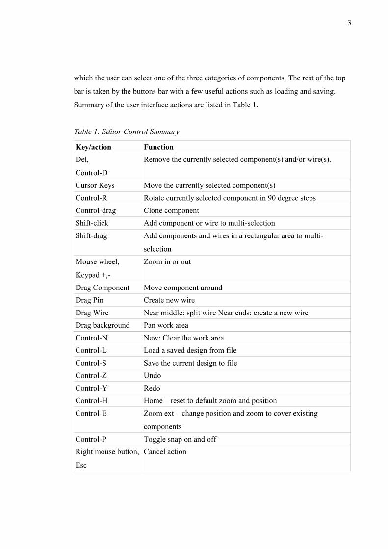
which the user can select one of the three categories of components. The rest of the top
bar is taken by the buttons bar with a few useful actions such as loading and saving.
Summary of the user interface actions are listed in Table 1.
Table 1. Editor Control Summary
Key/action FunctionDel,
Control-D
Remove the currently selected component(s) and/or wire(s).
Cursor Keys Move the currently selected component(s)Control-R Rotate currently selected component in 90 degree stepsControl-drag Clone componentShift-click Add component or wire to multi-selectionShift-drag Add components and wires in a rectangular area to multi-
selectionMouse wheel,
Keypad +,-
Zoom in or out
Drag Component Move component aroundDrag Pin Create new wireDrag Wire Near middle: split wire Near ends: create a new wireDrag background Pan work areaControl-N New: Clear the work areaControl-L Load a saved design from fileControl-S Save the current design to fileControl-Z UndoControl-Y RedoControl-H Home – reset to default zoom and positionControl-E Zoom ext – change position and zoom to cover existing
componentsControl-P Toggle snap on and offRight mouse button,
Esc
Cancel action
4
Some other aliases for controls have also been implemented, including several key
combinations for undo and redo. Mouse actions have been designed for a single-button
mouse, with keyboard alternatives provided where necessary.
2.2 Components, I/O
Components are created by simply dragging them from the toolkit to the work area.
Alternatively, if the user does not like dragging, it is possible to click on an item in the
toolkit and then clicking again on the work area to create the component. Right click or
the Esc key can be used to cancel the action.
As a shortcut for creating multiple copies of the same component, control-dragging a
component creates a clone. Once the component has been created, it can be removed by
clicking on it and pressing Del or Control-D.
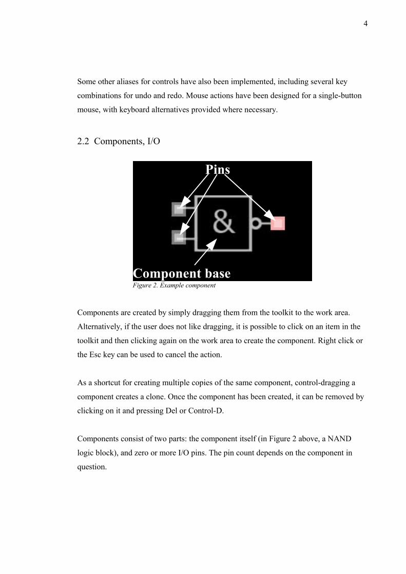
Components consist of two parts: the component itself (in Figure 2 above, a NAND
logic block), and zero or more I/O pins. The pin count depends on the component in
question.
Figure 2. Example componentComponent baseComponent base
PinsPins
5
Some components (such as labels) accept keyboard input. Clicking on a component
gives it the keyboard focus. If a component has any keyboard controls, they are listed in
the component's tool tip. Buttons always listen to the keyboard keys, and do not require
keyboard focus to function.
2.3 Editing Wires
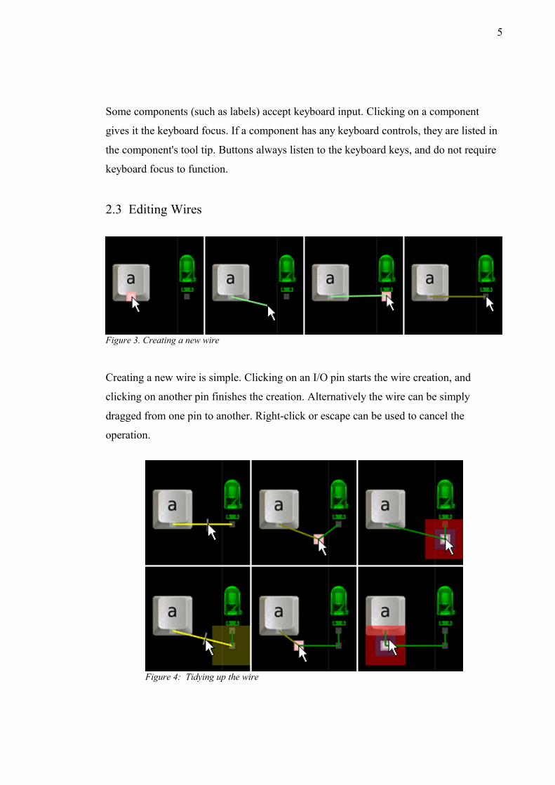
Creating a new wire is simple. Clicking on an I/O pin starts the wire creation, and
clicking on another pin finishes the creation. Alternatively the wire can be simply
dragged from one pin to another. Right-click or escape can be used to cancel the
operation.
Figure 3. Creating a new wire
Figure 4: Tidying up the wire
6
To tidy up, the wire can be split into several segments. This is achieved by moving the
mouse cursor close to the middle of the wire and dragging. These newly created
connection pins can also be used as the beginning or end of a new wire.
By default, Atanua has the “snap” option enabled, which limits the positions of
components to a grid of 0.5 coordinate units. As a reference, connection pins have an
area of 0.5 x 0.5 coordinate units. However, pins in many components do not align to
this grid perfectly, so it may be difficult to create perfectly 90-degree angle wirings in all
cases.
Wires can be removed by clicking on them to give them keyboard focus, and pressing
Control-D or the Del key. Deleting connection pins with only two connections joins the
two wires.
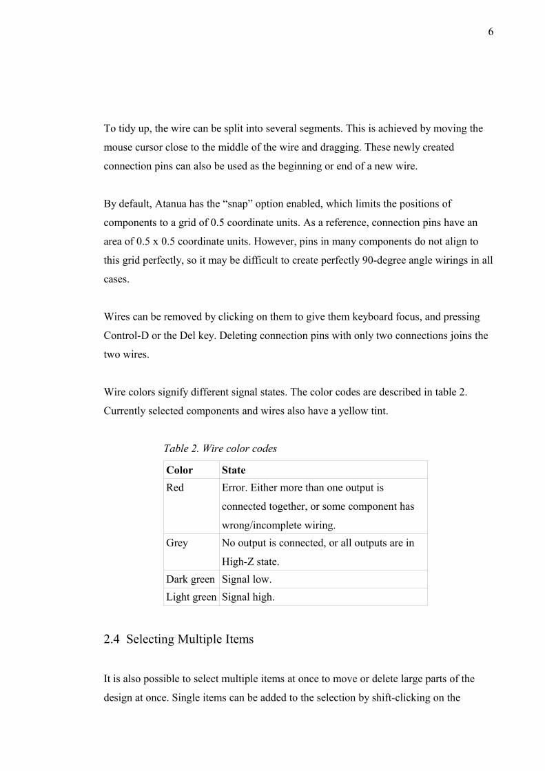
Wire colors signify different signal states. The color codes are described in table 2.
Currently selected components and wires also have a yellow tint.
Table 2. Wire color codes
Color StateRed Error. Either more than one output is
connected together, or some component has
wrong/incomplete wiring.Grey No output is connected, or all outputs are in
High-Z state.Dark green Signal low.Light green Signal high.
2.4 Selecting Multiple Items
It is also possible to select multiple items at once to move or delete large parts of the
design at once. Single items can be added to the selection by shift-clicking on the
7
component or wire. Multiple items can be selected at once by shift-dragging a rectangle.
Clicking on the work area or unselected component without shift clears the selection
from all items.
While multiple items are selected, you can drag on any of the selected items to move all
of the items, or press Control-D or the Del key to delete all of the items. Cloning of
multi-selected items has not been implemented.
3 Architecture
The software architecture in Atanua is a mixed C/C++ model, where OOP is only used
where necessary. Thus, the class hierarchy is rather simple. Most of the core code is
placed in global scope, including many of the data structures. STL containers, mainly
vectors, are used in many places.
Wrapping the global data into a class would make things slightly tidier, but this was not
seen as necessary, especially since there would only be one instance of said class, and
the members would most likely have been directly accessible.
3.1 Building Blocks
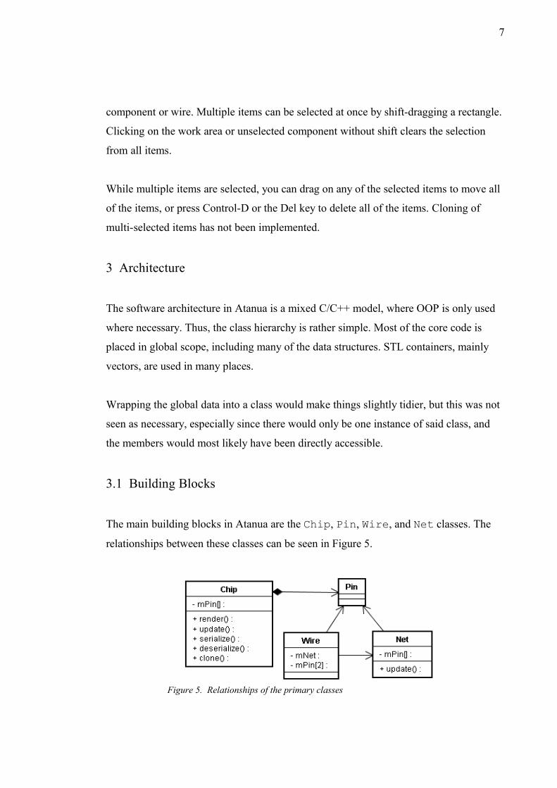
The main building blocks in Atanua are the Chip, Pin, Wire, and Net classes. The
relationships between these classes can be seen in Figure 5.
Figure 5. Relationships of the primary classes

8
All “components” the user sees in the editor are represented by a class extended from
the Chip base class. A chip contains zero or more pins, as well as the logic to update
their states. Most chips declare their pins in the constructor, update their state in the
update() call, and render the chip visually in render(). Some chips (such as
labels) contain data that needs to be saved – those define the serialize(),
deserialize() and clone() calls to store, restore and copy their internal state.
Apart from the interface function, a chip contains coordinate data, size and rotation
information, and a vector of pointers to pins. In practice the chips usually declare pins as
member variables for easy operation, but simulation only accesses the pins through the
pin-pointer vector.
A wire is a connection between two pins. Wires also know which net they belong to, but
this information is only used while building the net. Logically a net is a collection of
wires. In practice a net is a collection of pointers to pins, populated by a flood fill
algorithm based on the wire connections. Nets also contain a logic state. Pins tie
everything together. A pin contains a logic state that the chip is writing to the net and
some coordinate information relative to the chip they are owned by.
Figure 6. Collaboration graph of chip factories and chips
9
Chips are created by classes derived from ChipFactory, which create different chips
based on their name, following the abstract factory pattern[14,87]. From the logic
simulation core's point of view, all chips have an identical interface, so it does not need
to know any of the chip simulation specifics. The same chip name string is used for
saving the state, and is also used as the name listed in the toolkit. It is also used as the
default tool tip for the chip unless the chip defines one.
Currently there are two chip factories – BaseChipFactory, which constructs all of
the “built in” components, and PluginChipFactory, which handles the DLL plug-
in interface.
3.2 Plug-in Interface
The plug-in interface in Atanua went through several design iterations. The original idea
was to simply expose all of the information that is visible to all of the chip classes, but
this became difficult due to both the fact that chips use C++ features such as classes,
which may have caused problems over a DLL interface, but also since the pin vector
was a STL container, and potential linking of several different STL versions was seen as
a major problem.
In order to solve those problems, as well as to keep the DLL interface portable across
different compiler suites and onto different platforms, a pure C interface was designed.
This does not mean that a win32 plug-in would work on the OS X version, but rather
that it is possible to write plug-ins that compile on both platforms without any changes.
The plug-ins are able to access most of the data that is necessary to implement new
components. Some parts which require special knowledge of Atanua's internal state,
such as the buttons, may not be possible as plug-ins without extending the DLL
interface.

10
The plug-in interface serves two purposes. First and more obviously, it makes it possible
to create new components without having to re-compile the whole Atanua. Second, it
makes it possible to create components which have special requirements from the host
environment without imposing those requirements on Atanua. Additionally, the plug-ins
can be written using different compiler tool chains or even completely different
programming languages, as long as the DLL interface is compatible.
As an example, a simple 3-pin relay component plug-in, as well as its source code, is
provided with Atanua. The full source to this plug-in is included in Appendix 3.
Another plug-in that adds support for the Velleman K8055 USB experiment board is
also provided as a more complicated example, and can be found on the Atanua web site.
Building a chip directly into Atanua instead of a plug-in has two main advantages. First,
access to various helper libraries linked to Atanua, such as SDL[4], OpenGL[3],
TinyXml[15], file I/O, system dialogs, and various rendering functions, as well as access
to Atanua's internals such as data structures, textures and fonts, is much simpler.
Second, the plug-in interface does some data conversion, which imposes a slight
overhead.
3.3 File I/O
The standard c “fopen”-style file I/O is wrapped inside the class File. This serves
several purposes. First, the class contains easy serialization helper functions to save and
load 8, 16 and 32 bit values. These functions handle any needed byte order translations.
Second, the File class can and has been overloaded to a MemoryFile class, which
stores the data in memory.
The implementation of the MemoryFile uses a vector of 8-bit characters. This is
quite inefficient, but due to the small amounts of data handled, it is not considered to be
a problem. Should Atanua require huge amounts of memory and slow down, the
MemoryFile implementation is one of the easiest targets for optimization.
11
3.4 Saved Files and Undo
Atanua supports two different file formats. The original design file format was a custom
binary, which was replaced with a more flexible, human-readable XML format. The
binary format support was retained primarily due to its use in the undo/redo
functionality, but also for backwards compatibility.
Every time the user does something potentially destructive, for example creates or
deletes a component, the whole state is saved in a memory buffer in the binary format.
There is no hard-coded upper limit for the saved states, and thus the user can undo all
the changes until application startup state is reached, and redo back. Due to the small
size of the binary format, each saved state for even relatively complicated designs only
takes a few kilobytes of memory.
The binary format has a smaller footprint and is faster to process, but the XML has
several advantages as the main design file format. It tends to survive transfer as e-mail
attachments better, is human readable, other programs may also process (or generate)
the file, and additions to the format do not require special code to retain backwards
compatibility.
The XML file format support is built using the TinyXml open-source library.[15] The
structure of the XML file is as follows:<?xml version=”1.0” ?><Atanua ...>
<Chip ...>...<Wire ...>...
</Atanua>

12
There may be any number of Chip or Wire tags, but all Chip tags referred to by the Wire
tags must come before the Wire tags. The parameters of the Atanua, Chip and Wire tags
are described in tables 3, 4 and 5.
If errors occur during design file load, such as invalid wire parameters or unknown chip
name, the user is asked whether to continue trying to load the rest of the file. When
loading a design which uses an unknown plug-in, the user can see the name of the
unknown part, and if further loading is attempted, parts of the design may still be useful.
Table 3. Parameters of the Atanua tag
Parameter DescriptionVersion Optional. Version of Atanua used to save the
file.ChipCount Optional. Number of chips in the design.WireCount Optional. Number of wires in the design.key Optional. Used to validate homework.scale Optional. Default value 24. Defines the fixed
point format for coordinates in the file. Value
24 means the 8.24 format.
Table 4. Parameters of the Chip tag.
Parameter DescriptionName Name of the chip. Used as the key to create
the class with.xpos X coordinate position in fixed point format.ypos Y coordinate position in fixed point format.rot Optional. Default value 0. Rotation clockwise
in 90 degree steps.key Optional. Used to validate homework.Tag content Hexadecimal data in custom format defined
by the chip. Not used by most chips.

13
Table 5. Parameters of the Wire tag.
Parameter Descriptionchip1 The order number of the first chip. First chip
defined in the save file is number 0.pad1 The pin number on the first chip. Exact
location depends on the chip, and does not
follow data sheet pin numbering.chip2 The order number of the second chip. First
chip defined in the save file is number 0.pad2 The pin number on the second chip. Exact
location depends on the chip, and does not
follow data sheet pin numbering.key Optional. Used to validate homework.
Saving the information of which version of Atanua was used to save the design file has
proved to be very useful. When users report problems, they often forget to mention the
version they are using. Chip and wire counts are stored for informative purposes only,
and Atanua does not care about the values when loading.
Coordinates are saved in fixed point format in order to avoid potential portability issues.
This was originally a real issue due to the binary file format – the XML format could
have used a more human-readable format, but compatibility with the binary format was
retained.
If a chip implements the serialize() and deserialize() functions, they save
and load their internal states to a memory file object. The data is stored in the XML file
encoded in hexadecimal text format inside the Chip tag.
Typical pin numbering for a chip is to have the chip oriented sideways with zero pin on
the left bottom and to go through the pins left to right top row first, then second row left
to right.

14
3.5 Configuration file
Atanua's configuration file, atanua.xml, contains options with which different editing
capabilities can be tuned. List of any plug-ins the user wishes Atanua to load are also
included in the file. The structure of the configuration file is as follows:<?xml version=”1.0” ?><AtanuaConfig GeneratedWith=”Atanua [version]”>
...</AtanuaConfig>
Several different configuration options appear between the AtanuaConfig tags. These
tags and their parameters are described in table 6.
Table 6. Configuration File Tags
Tag Parameter(s) DescriptionAntialiasedLines value Default 1. Controls use of thick and antialiased
lines. Turning this off may help in compatibility
and performance issues.PropagateInvalidState value Default 1. Controls whether chips propagate
invalid state or turn to High-Z mode when
errors are detected.CustomCursors value Default 1. Controls use of custom cursors such
as scissors. Turning this off may help in
compatibility issues.WireFry value Default 1. Controls whether the wire frying
behavior is enabled.ToolkitWidth value Default 115. Controls the toolkit width.MaxPhysicsMs value Default 40. Shrinking may make Atanua more
responsive, but reduces simulation accuracy.InitialWindow width, height Default 800, 600. What size the Atanua
window should be at startup.TooltipDelay value Default 1500. Tool tip delay in milliseconds.
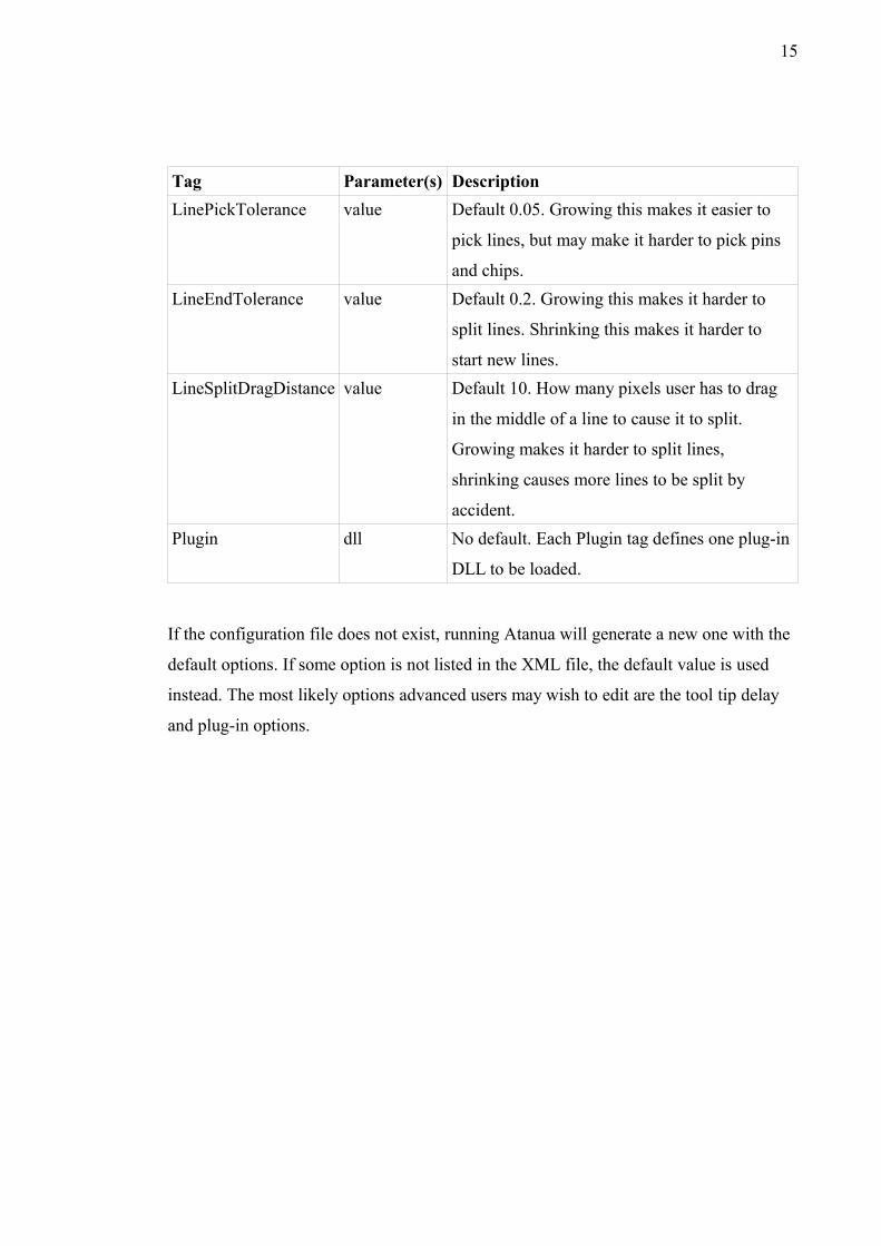
15
Tag Parameter(s) DescriptionLinePickTolerance value Default 0.05. Growing this makes it easier to
pick lines, but may make it harder to pick pins
and chips.LineEndTolerance value Default 0.2. Growing this makes it harder to
split lines. Shrinking this makes it harder to
start new lines.LineSplitDragDistance value Default 10. How many pixels user has to drag
in the middle of a line to cause it to split.
Growing makes it harder to split lines,
shrinking causes more lines to be split by
accident.Plugin dll No default. Each Plugin tag defines one plug-in
DLL to be loaded.
If the configuration file does not exist, running Atanua will generate a new one with the
default options. If some option is not listed in the XML file, the default value is used
instead. The most likely options advanced users may wish to edit are the tool tip delay
and plug-in options.

16
4 Logic simulation
4.1 The Logic Simulation Loop
The logic simulation is made real-time by calling the update() function of every chip
and every net 1000 times per second. This is achieved by keeping count of the “physics
time”. The physics time is a simple counter which is increased every time physics
iteration is executed.
Figure 7. Main physics simulation loop

17
Before performing the updates on nets and chips, two checks are made. First, there are
situations where the main loop has not run for a long time – such as when the user uses
the file open dialogs. In such cases we reset the physics time to the current time and
move on. Without this check the simulation may take a long time to catch up.
Next we check if any time has passed. If less than 10ms has passed, we tell the operating
system to put our process to sleep for a while, and skip the logic simulation and
rendering completely, thus saving CPU power. We save CPU power further with
another sleep instruction after rendering, regardless of the simulation speed.
After these initial checks we enter the update loop. For each update round the physics
time is increased by 1ms. Once it has caught up with real time, we exit the loop. As a
precaution we also check if this update loop is taking too long, as it is possible to create
so heavy a circuit that it cannot be updated in real time. This is surprisingly easy when
using plug-in components. After doing updates for over 40ms, we exit the loop. If the
simulation is taking exactly 40ms, this should ensure a frame rate of approximately 25
frames per second. The safety value of 40ms can be changed in the configuration file.
Due to the internal update rate of 1000Hz, the maximum clock rate (signal change from
high to low to high again) is 500Hz.

18
4.2 Logic States
Pure Boolean logic defines two states – true and false. Atanua requires a few more
states, and both pins and nets have their own definition of logic states.
Table 7. Net logic states
State DescriptionNC Not connected – no active output pins are
connected to this net.INVALID Either more than one output pin is connected
to this net, or the output pin is sending
'invalid' state. HIGH One output, writing 'high' signal.LOW One output, writing 'low' signal.
The logic states for nets, as described in table 7, are straightforward. The only one with
no physical analogue is the “invalid” state, which is included to let the user know when
something is clearly wrong. In such a case a real-world circuit might either work, not
work, or work randomly depending on timing. In a software simulation it is better to
signal the problem directly.
Table 8. Pin logic states
State DescriptionHIGHZ Pin is in “High-Z” state, neither reading nor writing a
signal. READ Pin is meant for chip input. This is the default.WRITE_HIGH Pin is writing “high” signal to the net.WRITE_LOW Pin is writing “low” signal to the net.READ_OR_WRITE_HIGH If it is the only pin writing to the net, write “high”.READ_OR_WRITE_LOW If it is the only pin writing to the net, write “low”.PROPAGATE_INVALID Propagate “invalid” signal onwards.

19
The pin logic states, as listed in table 8, are somewhat more complicated. Physical
components are not defined by logic states but instead by their capability of feeding or
sinking current. Most of the simple parts can be defined with the “READ”,
“WRITE_HIGH” and “WRITE_LOW” signals. Some components have a capability of
“turning invisible” to the circuit by changing its I/O pins into a “High-Z” mode, in
practice disconnecting the chip from the circuit. The “PROPAGATE_INVALID” signal
is sent if some required input wiring is not connected, or an “INVALID” state is read
from the net to which some input is connected.
There are also some devices that define their pins as both read and write. The 2051, or
any 8051-based microcontroller, defines “read” pin by writing a high signal.[6,3]
Without looking at the instructions the microcontroller is executing, it is impossible to
know whether it wants to write a high signal or read a signal – or perhaps both. Another
example is the 74LS47 BI /RBO signal, which at the same time can be blanking input
or ripple blanking output.[7,3]
4.3 Necessary Imperfections
Cross-connecting NAND or NOR gates is a common circuit necessary for many of the
basic building blocks of logic circuits, including latches and flip-flops. Unfortunately
such a configuration introduces a racing condition in the circuit. This racing condition
also exists in real-world TTL circuits, but is more severe in a pure logic simulation as all
Figure 8. Cross-connected NAND gates

20
of the simulated components are “ideal”, and as can be seen from table 9, nobody
“wins” the race.
Table 9. Four first cycles of cross-linked NAND states
Cycle Next A Next B1 1 ∧ B=0 1 ∧ A=02 1 ∧ B=1 1 ∧ A=13 1 ∧ B=0 1 ∧ A=04 1 ∧ B=1 1 ∧ A=1
Several different solutions to this problem were tested. Simply dropping random signal
change when one is requested solves the problem, but introduces large amount of bugs.
Some chips such as 74163 send signals that are only one clock cycle long, and such
signals could easily be lost.
Another idea was to make some of the wires “slow”, by adding a buffer to them. This
does not solve the problem, as the racing condition is kept alive, but with a delay. This
is true regardless of whether the buffers are the same size, random, or unique. The third
idea was to introduce a start-up delay to the nets, which solves the problem, but only for
the initial state, and if any such racing condition occurs later on (and it is easy to create a
case where this is true), the problem would persist.
In real-world TTL circuits, there are no discrete logical states. The gates try to pull and
push the current to different levels, and due to the tiny imperfections of the parts, one of
the gates “wins”.[12] To simulate this, we have to introduce a “bug” into the simulation.
The nets track high-frequency changes and there is a 50% chance every 50 switches
between high and low signal states that the signal state change is dropped. In practice
this reduces the maximum clock rate by 1%, which can be considered as an acceptable
failure rate, especially as it has been seen to be an effective solution to the racing
conditions.

21
5 User Interface Technologies
The user interface is the most critical part of Atanua. Even if the logic simulation did
not work, the user interface could be used to draw logic circuit diagrams. Without a
working user interface, the logic simulation itself would be worthless.
The implementation of the user interface is also more complicated than the logic
simulation. There is more code in the simulation part, but it is rather repetitive as most
of the simulated components work in a similar manner.
5.1 IMGUI
The user interface architecture is based on the “IMGUI” paradigm. While not my own
invention[8;9,34-36], the best reference as of this writing is my own online tutorial[5].
IMGUI stands for Immediate Mode Graphical User Interface. Traditional user interface
architectures, often referred to in relation to IMGUI as “retained mode user interfaces”,
are based on “widgets”, such as buttons, scroll bars, and so on.
In a traditional system these widgets are created by the application, owned by some kind
of windowing system, communicated with using asynchronous or synchronous
messages, rendered by the windowing system with little or no control from the
application, and have to be cleaned up afterwards. As a result, the handling of a single
user interface component is split into at least three places – initialization, event
handling, and cleanup.
22
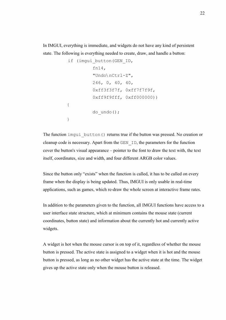
In IMGUI, everything is immediate, and widgets do not have any kind of persistent
state. The following is everything needed to create, draw, and handle a button:if (imgui_button(GEN_ID,
fn14, "Undo\nCtrl-Z", 246, 0, 40, 40,0xff3f3f7f, 0xff7f7f9f, 0xff9f9fff, 0xff000000))
{do_undo();
}
The function imgui_button() returns true if the button was pressed. No creation or
cleanup code is necessary. Apart from the GEN_ID, the parameters for the function
cover the button's visual appearance – pointer to the font to draw the text with, the text
itself, coordinates, size and width, and four different ARGB color values.
Since the button only “exists” when the function is called, it has to be called on every
frame when the display is being updated. Thus, IMGUI is only usable in real-time
applications, such as games, which re-draw the whole screen at interactive frame rates.
In addition to the parameters given to the function, all IMGUI functions have access to a
user interface state structure, which at minimum contains the mouse state (current
coordinates, button state) and information about the currently hot and currently active
widgets.
A widget is hot when the mouse cursor is on top of it, regardless of whether the mouse
button is pressed. The active state is assigned to a widget when it is hot and the mouse
button is pressed, as long as no other widget has the active state at the time. The widget
gives up the active state only when the mouse button is released.

23
A simple test of the hot/active behavior is to push a button in windows, and move the
mouse outside the button's area. The button pops back up. The button is still “active” –
you can move the mouse back on top of the button and it goes back to the “pushed”
state. If you release the mouse button while outside the button area, the button's function
is not activated.
In order to separate between different widgets, every widget has to have a unique ID.
This ID must, however, be the same for each of the widgets in every frame. This is
achieved with the GEN_ID macro. In this case the macro simply returns the line in the
source code where the button is called, which is enough as long as only one widget is
called per source code line, and only from one source file.
Some widgets, such as the scroll bar or the text field, require some persistent state.
These kinds of variables are owned by the caller, and no message passing, additional
memory allocation or data copying is necessary.
Since all of the components in Atanua are also IMGUI widgets, the generation of unique
IDs is handled differently. Macros CHIP_ID and WIRE_ID generate unique widget
IDs for chips and wires based on their positions in the global gWire and gChip vectors. The chip ID also has the currently hot pin encoded in the same value.
Information can be extracted from the IDs using the macros IS_CHIP_ID,
IS_WIRE_ID, GET_CHIP_ID, GET_WIRE_ID and GET_PIN_ID. These macros
decode the desired information from the 32-bit ID.
The user interface state structure in Atanua also contains various variables related to
keyboard handling, mouse wheel, and the mouse position at the time the mouse button
was pressed. These additional members make it possible to implement features such as
keyboard input, zooming, dragging, or dragging while the control key is pressed.
The negative side of IMGUI is that rendering and widget logic tends to be mixed, which
may result in confusing code. Since the code which handles chips, pins and wires is
basically one huge IMGUI widget, it can be difficult to understand.

24
Apart from the chip, pin and wire manipulation code, the slider used to scroll the toolkit
contents is the most complicated IMGUI widget used in Atanua. The calculation of the
height of the “thumb” part, which is the bit that the user moves to scroll the toolkit, is
perhaps the most interesting purely mathematical problem that was solved in this
project.
We want the height of the thumb to give the user an idea of how much of the available
data is seen. Thus, the height of the thumb in relation to the height of the component is
the same as the relation of the component and the available data. However, the thumb
height reduces the amount of available scrolling space. Thus, we get the formula
t = h − t ⋅ hm
t is the height of the thumbh is the height of the componentm is the maximum value
(1)
When solved, this simplifies to
t = h2
m h(2)
5.2 Tool Tips
Tool tips are small windows of text that pop up near the mouse cursor when the mouse
has been still for a while. The default delay, which can be edited in the configuration
file, is set at 1500ms. The tool tips are the primary way in Atanua for the user to get
information about different components and I/O pins without referring to the data sheet.
The delay is relatively long by default as the tips may confuse new users. Advanced
users may wish to reduce the delay.
The tool tips for chips show the headline of the data sheet, such as “Triple 3-input
NAND Gate”[10,1]. Each pin has a tool tip that shows the pin number, as well as the
25
information given in the data sheet. In many cases this is enough by itself, but
sometimes the pin descriptions can be rather cryptic, such as BI /RBO [7,3], and will
require the user to refer to the data sheet to understand how the I/O pin in question is to
be used. Tool tips for the wires show the current state and a short description of what the
state means. Tool tips are not provided for other user interface elements.
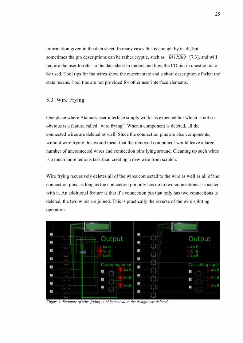
5.3 Wire Frying
One place where Atanua's user interface simply works as expected but which is not so
obvious is a feature called “wire frying”. When a component is deleted, all the
connected wires are deleted as well. Since the connection pins are also components,
without wire frying this would mean that the removed component would leave a large
number of unconnected wires and connection pins lying around. Cleaning up such wires
is a much more tedious task than creating a new wire from scratch.
Wire frying recursively deletes all of the wires connected to the wire as well as all of the
connection pins, as long as the connection pin only has up to two connections associated
with it. An additional feature is that if a connection pin that only has two connections is
deleted, the two wires are joined. This is practically the reverse of the wire splitting
operation.
Figure 9. Example of wire frying. A chip central to the design was deleted.
26
Combined, these two features work surprisingly well. Deleting a central component of a
complex circuit results in a clean design, with little or no additional clean-up required
before the work on the design is resumed.
If wire frying is not desired, it can be avoided in two ways. The first is to delete the
wires connected to the chip before deleting it. A more permanent way is to disable the
option in Atanua's configuration file.
5.4 Picking
Picking is the operation of establishing which item the mouse is pointing at. In practice
this means that we have to go through all of the user interface elements and see if the
mouse cursor position happens to collide with it.
At times more than one item is under the cursor, but due to the way IMGUI works, only
the first one can get the active state, even if all of them are “hot”. The negative side
effect of this is that if two components have been dragged over each other, the bottom-
most has the priority. This is not intuitive, but happens rarely in actual use.
While editing, wires often go over components. It is in fact possible to have a wire that
is completely on top of a single component. In some cases such a connection is
desirable, such as with the 74LS90 where different operation modes are selected by
connecting certain chip outputs to certain inputs of the same chip[11,2], so simply
making such a connection illegal was not an option.
We solve this problem by checking picking against wires before the components. The
components also tend to have much bigger area, so it is improbable that wires would
completely occlude a component. As a special case, wires are rendered after the
components, so the user can see the wires even when they cross the components.

27
There are two kinds of picking (single and rectangle) and two kinds of pickable
primitives (rectangles and line segments). Single-picking of rectangles is trivial. Finding
whether a point is inside an axis-aligned rectangle simply means checking if the x and y
coordinates of the point lie between the x and y coordinates of the top left and bottom
right corners of the rectangle.
Single-picking a line segment is more complicated. In Figure 10 we want to find out the
distance from the line segment “a” to the point that is pointed at by the arrow “e”. There
are three measurements that we have to take into consideration. First is the distance “g”
from the infinitely long line “b” to the point “e”. The two others are distances from the
end points of the line segment – “c” and “f” – to the point “e”.
We have to consider the end points since the point might be right on the infinite line “b”
but not near the line segment “a”. If the distance to one of the end points is longer than
the whole line segment length, we know that the value we are looking for is the distance
to the closest end point “d”; otherwise the distance is “g”.
Multi-picking rectangles requires a rectangle-rectangle overlap test. This is done by
checking if all of the vertices of the first rectangle are either to the left, above, to the
right or below the second rectangle. If any of the tests succeed, the rectangles do not
overlap.
For the rectangle-line overlap test I adapted the line segment to axis-aligned bounding
box collision test from [13,183], by reducing it to two dimensions.
Figure 10. Single-picking a line segment
a
b
b
c
d
e
f
g

28
5.5 Chip Rotation
The rotation of the chips was implemented fairly late in the development process. The
rotation was limited to 90 degree steps so that more complicated picking code was not
required. Rotation is, along with deletion, the only action the user can take which has to
be done on the keyboard and for which there is no hint in the interface. Adding a button
to the user interface would not have worked, since the button would have taken the
focus from the selected component. Unlike deletion, which is intuitively linked to the
Del key, there is no obvious key for rotation. Chips can be rotated by pressing Ctrl-R
while a chip is selected. Rotating multi-selected items has not been implemented.
The rotation affects rendering, and picking of chip geometry, and pin positions. Instead
of calculating the new positions for all of the pins every time a pin was being picked, the
rotated positions and sizes of chips and pins are stored in the chip and pin structures. All
of the rotation-related changes were made in the simulation core, and no changes were
needed in any of the already implemented chips. Since the rendering code is outside the
simulation core, the rotated rendering of the chips was done using OpenGL matrices.
6 Homework Validation Tool
There was one unexpected request from the teachers after the first versions of Atanua
were in testing. Several teachers requested some way of detecting whether students were
copying homework from each other, and submitting it as their own. Even though
making such a system foolproof was impossible, some kind of implementation was
clearly still desirable.
The only way to make such a tool work would be to require constant network
connection and to keep remote copies of everything. This was, however, not feasible.
Instead, a simple validation scheme was implemented, based on saving timestamps of
actions in the save file.
29
By analyzing these time stamps, as well as components used, it is possible to give a
fairly accurate analysis on how identical different save files are. As an additional side
effect, the approximate time that was spent working on a circuit can be estimated.
It would be simple to expand this mechanism by using stronger hashing algorithms,
encrypt the design files, store the undo data, etc, but none of these approaches would
seriously increase the difficulty of “hacking” the design files, since the users have access
to the tool which creates the files. On the other hand, doing any of the above would have
negative side effects.
While the system is relatively simple, hacking it would most likely require more
knowledge and effort than simply doing the homework. Additionally, people interested
in hacking the validation system are most likely the ones who are also interested in the
subject, and thus not likely to try to cheat. In order to reduce the chances of cheating, the
analysis tool and further details are only available to teachers and only on request.
7 Simulation Examples
Apart from the user interface and core simulation system, a large part of the project was
to simulate various real-world components. The implementations of two parts are
covered here as examples. The full source of the AND gate simulation is also included
in appendices 1 and 2.
7.1 A Simple Example – 74LS08
The 74LS08 is a 14-pin chip that contains four 2-input AND gates[16]. The
implementation of the chip is in the source files Chip7408.h and Chip7408.cpp.

30
7.1.1 Header File
The header file describes that the class defines three Pin arrays, for input a, input b and
output pins. Each of the arrays is four wide – one set for each of the AND gates in the
component. The class also defines that the class has one texture, with an integer handle.
The 7408 only defines the minimal set of interface functions: render() and
update().
7.1.2 Constructor
The Implementation of the constructor calls the utility “set” function to define the
default coordinates, width and height, and the tool tip string of the chip.
Afterwards it pushes a pointer of each of the pins to the chip's pin vector. Then the “set”
function for each of the pins is called to set up their state: the chip-relative positions of
the pins, tool tip strings, and a pointer back to the chip. This is done top row first, then
the bottom row, left to right.
The pins could have been allocated from heap and pushed to the pin list, but that would
both complicate the access to the pins in the logic update and would require explicit
cleanup. There is also no reason to define the pins in this specific order.
Finally the constructor loads the texture for the chip. The textures are cached, so even
though every copy of the chip seems to load a new copy of the texture, only one copy is
kept in memory. The 7408 uses a generic 14-pin chip texture.

31
7.1.3 Rendering
The rendering function uses the texture to draw the chip, and draws the chip designation
“74LS08” on top of it using a bitmap font at 95/255 opacity and a font height of 0.75
units, making the result look like the designation was painted on the chip. No special
handling of chip rotation is performed here – the main rendering loop uses OpenGL
matrices to rotate the chip before rendering.
7.1.4 Update
The update function handles each of the four AND gates separately. For each gate, the
inputs are first validated. For gates with non-connected input pins or pins that are
receiving the invalid signal, output is set to a value stored in the global configuration. In
practice the output is set to either INVALID (the default) or HIGHZ. Neither of these is
what would happen with real hardware, but are done so that any problems with the
circuit are very clear to the user.
After validating the input pins, pins A and B are checked for either HIGH or NC state,
and if both pins have either of these states, the output pin is set to send HIGH signal.
Otherwise LOW signal is sent. The default state for all pins is to be in READ state. Thus,
any pins for which the chip does not change pin state remains in the READ state.
7.2 A Complex Example – 89C2051
The 2051 is the most complicated chip simulated in Atanua. Not only does it use a
separate simulation code base[1], but it also demonstrates several of the more
complicated simulation techniques. The implementation of the Atanua part of the 2051
can be found in Chip2051.h and Chip2051.cpp.
32
The 2051 in Atanua is modeled after Atmel AT98C2051[6], a 20-pin variant of the 8051
microcontroller. None of the advanced functionality of the Atmel part, such as the
analog comparator, is simulated. The features of the 8051 emulation core can be found
at [1].
Since Atanua's simulation runs at a fairly low clock rate, we compensate by running the
8051 simulator core so that each 8051 instruction is executed in a single clock cycle,
instead of the normal 12-24 clock cycles.
7.2.1 Header File
Like the 7408, the header file of the 2051 part defines pins – 8 pins for the I/O port 1
and 7 pins for the I/O port 3. Additionally the chip defines reset and clock pins.
The 8051 emulation core needs the em8051 structure and memory area buffers, so they
are also defined as member variables.
Similar to the 7408, one texture is defined. Unlike the 7408, the 2051 is a synchronous
chip, and requires a variable for tracking the clock pin state. Due to the way the reset pin
is specified, another counter is required for it as well.
The 2051 defines the full set of interface functions: render(), update(),
serialize(), deserialize() and clone().
7.2.2 Constructor
The implementation of the 2051 constructor is fairly similar to the 7408. Pins are
pushed to the pin list, parameters are set, tool tips defined, and so on. Additionally the
8051 simulation core data is initialized, and the clock and reset counter variables are set

33
to zero. The tool tip for the chip includes instructions on how to load program data to
the 2051 flash.
7.2.3 Rendering
The rendering function draws the chip. It also handles the keyboard input. The keyboard
input would logically belong to the update-function, but simply because the keyboard
does not require updates at 1000Hz it makes more sense to handle it here.
First the routine checks if it is the component which currently has the keyboard focus,
and after this fact has been established, checks if the key “L” has been entered. If so, it
calls the platform-specific file open dialog, and asks the 8051 emulation core to load the
data. No errors are reported.
7.2.4 Update
The update function first checks if reset pin has been connected, or is low, and sets all
output pins to high as dictated by the data sheet[6,3]. If the clock pin is not connected,
no further action is taken.
If the clock signal is low, the most recent clock signal variable is set to 0. If the signal is
high, and the most recent signal was 0, we set the most recent signal to 1 and do the
actual synchronized processing. If the reset pin is not connected or receives low signal,
the counter is increased and no further processing is done. If the counter is over 1, the
8051 core is reset[6,3].
Now that the reset pin functionality is covered, we tick the 8051 emulation core until it
reports having executed an instruction. When the 8051 simulation core needs to read
information from an I/O pin it uses a callback. In this callback we check if the pin is
34
connected to a net and the net signal is not low, and report the result back to the 8051
simulation core.
After the instruction is performed, we update the I/O pin states to reflect the I/O states in
the 8051 simulation core. Since from the outside the 8051 defines “reading” state by
writing a logical true to a pin[6,3], we have to define the pins in the less-strict logic
states READ_OR_WRITE_HIGH and READ_OR_WRITE_LOW. We cannot use
WRITE_LOW state for the low state since some 8051 programs sometimes turn off the
read pins, which would confuse the simulation.
7.2.5 Serialize
Serialization of the internal state is required for both save files and for the undo/redo
functionality. For the 2051 it is enough to serialize the program memory, which was
loaded by the user from an Intel HEX format file.
Since most programs do not take the whole 2kB of available space, it does not make
sense to store the whole memory every time. Instead, trailing zeros are checked to find
how much of the program memory is actually in use.
After this is known, the size is first stored as an integer, and the data itself is stored byte
by byte through the file handle. The file I/O routines handle any potential byte order
issues, and can store the data to either a memory buffer or to an actual disk file.
7.2.6 Deserialize
The reverse operation is simpler. First we clear the memory to zero, read the data size as
an integer and then the data itself byte by byte.
35
7.2.7 Clone
When the chip is cloned, the user expects the internal state to remain the same. Thus, the
code memory is copied to the newly created object.
8 Development Process
Atanua's development process was iterative. After the initial version was developed, a
new version was released almost every day for a month, integrating suggestions from
users, fixing bugs and including new simulated parts.
8.1 Initial Research
The project was researched for approximately six months before starting to build the
program. Most of this research was brain work, and discussions about how the system
would work with electronics experts, such as Jari Korhonen, Director, HW Platforms
R&D Core Networks, HW Platforms R&D Operations, Nokia Corporation [personal
communication, September 22, 2007].
The general desire was to make the source base portable to other platforms, and thus the
original idea was to write it using wxWidgets, a cross-platform user interface library[2].
Due to the amount of custom user interface code required by Atanua, wxWidgets was
abandoned, and the project was briefly attempted with MFC, a windows-only toolkit,
before discarding it as well.
The main advantage of having used wxWidgets or MFC was support for clipboard
operations and easy handling of large amounts of text. The original design included a
sub-window which would have included information about the active chip, possibly
directly the data sheet for the part. This approach was dropped as acquiring the rights to
redistribute the data sheets was found to be quite difficult, and it is best to have the data
sheet in a separate window in any case.

36
In the end the user interface was built from scratch using OpenGL[3] on top of SDL[4],
both of which are supported in many platforms. All user interface components were
written from scratch based on the IMGUI paradigm.[5] The only platform-specific code
required by Atanua are for the file open/save dialogs. Using hardware acceleration also
enabled many neat features such as easy extreme zooming, anti-aliased lines,
transparency effects and things like glowing LEDs.
The portability of the code base was validated by making a version for OS X running on
a PowerPC CPU. The OS X version has a completely a different compiler tool chain, a
CPU with a different byte order and most importantly a different operating system. On
top of the platform-specific dialog functions, only a few byte order issues had to be
fixed to build Atanua in an entirely different environment. Later Atanua was also ported
to 32-bit Intel Linux.
8.2 Development Cycle
Once development was under way, the process was handled in rapid iterative cycles.
The first released version took approximately one week to build, at which point the
program already supported basic logic gates, LEDs, buttons and clocks. Subsequent
versions, released almost daily, added new components, including more complicated
logic blocks, various 74-series chips and new editing functionalities such as splitting of
the wires, as well as bug fixes.
Every component that the user can use was tested by making a new project in Atanua
and building a simple circuit based on that component. This revealed most of the
problems with said components before release. All of these tests are also included in the
release package to be used as reference. While the primary reason for building the tests
was to check if the newly created component was functional, it also stressed the general
editing capabilities, revealing bugs and missing functionality.

37
Many of the implemented features that were built were based on user feedback. As
obvious as it sounds, resizing of the window was a feature that was only added after user
requests. Several suggestions were given by Christoffer Enedahl, Programmer /
Designer, Amfora Training AB, Tomas Pettersson, Software Engineering Student,
Linköpings Universitet, Ron Bunce, Independent Software Professional, Andrew Hood,
Electronics Hobbyist, and Ola Frid, Student, Computer Science and Engineering,
Chalmers University of Technology [personal communication, January 13 – February
27, 2008].
8.3 Release Process
The project followed a strict release process to ensure quality releases.
1. Change version number.
2. Make a full rebuild in release mode.
3. Create a new release directory by copying the most recent one to include all of
the required DLLs.
4. Copy the new executable, all tests and all data, regardless of if they have
changed, to the new directory.
5. Delete configuration file.
6. Launch executable to create a new configuration file. Check that the version
number has changed. Test some of the most recent functionality.
7. Create a ZIP archive, upload it to the WWW server.
8. Edit TODO list and web page to cover latest developments.
9. Upload web page.
10. Archive all source material, and upload it to a remote server as off-site backup.
Due to this process, the only fatal errors that were found in a released version were such
that were not reproducible locally, and all data files were up to date.
If a source repository such as CVS or SVN was used, step 10 would not be needed, and
would be replaced by source submit phases instead.

38
9 Conclusions
In general the project has been very successful, and users in general have given positive
feedback on the ease of use, and other schools beside EVTEK have expressed interest in
using it as a teaching aid. Atanua fulfills several needs in teaching of electronics and
digital circuits. Even without the simulation, it can be used to draw logic graphs.
Several people have noted that the interface is almost like a game. One possible
development direction would be to turn Atanua into an interactive tutorial with different
kinds of scenarios, with game play similar to The Incredible Machine[17]. In addition to
building circuits from scratch, partial circuits could be given to the user to fix.
Other obvious developments would be to simulate more chips, including different LCD
screens. Various microprocessor and microcontroller core simulations could be ported
over from the MAME project, and if done as plug-ins, conflicts with the MAME
distribution license could be avoided[18]. New plug-ins to support external peripherals
could be added.
Some of the suggestions that were not implemented but could be interesting include
importing and exporting net lists, so that the results of the design could be imported or
exported to other tools. Several of the 8051 simulator features could be used better,
including register views.
Finally, the graph drawing part of Atanua could be used to drive completely different
kinds of projects, such as procedural audio or texture generation / filtering systems.

39
References
1. Jari Komppa. 8051 Emulator [online]. Finland; September 5, 2006.
URL:http://iki.fi/sol/8051.html. Accessed February 11, 2008.
2. wxWidgets [online].
URL:http://wxwidgets.org. Accessed February 11, 2008.
3. OpenGL – The Industry Standard for High Performance Graphics [online].
URL:http://opengl.org. Accessed February 11, 2008
4. Simple DirectMedia Layer [online].
URL:http://libsdl.org. Accessed February 11, 2008
5. Jari Komppa: www.iki.fi/sol – tutorials – IMGUI [online]. Finland; October 30,
2006.
URL:http://iki.fi/sol/imgui/. Accessed February 11, 2008.
6. Atmel Corporation: AT89C2051 - 8-bit Microcontroller with 2K Bytes Flash.
Data sheet, June 2005
7. Fairchild Semiconductor Corporation: DM74LS47 – BCD to 7-Segment
Decoder/Driver with Open-Collector Outputs. Data sheet, March 1998
8. Casey Muratori, Molly Rocket, Inc: IMGUI [online]. July 4, 2005.
URL:http://www.mollyrocket.com/video/imgui.avi. Accessed February 12,
2008.
9. Game Developer Magazine, September 2005, Volume 12, Number 8
10. Fairchild Semiconductor Corporation: DM74LS10 – Triple 3-input NAND Gate.
Data sheet, August 1986
11. Fairchild Semiconductor Corporation: DM74LS90 – Decade and Binary
Counters. Data sheet, August 1986
12. Michael Stutz: NOR gate S-R latch: DIGITAL INTEGRATED CIRCUITS
[online].
URL:http://www.allaboutcircuits.com/vol_6/chpt_7/3.html. Accessed February
13, 2008.
13. Ericson, Christer. Real-Time Collision Detection. Morgan Kaufman, Elsevier
Inc, 2005.
40
14. Gamma, Erich; Helm, Richard; Johnson, Ralph; Vlissides, John. Design
Patterns: Elements of Reusable Object-Oriented Software. Addison-Wesley,
1994.
15. Lee Thomason: TinyXml Main Page [online]
URL:http://www.grinninglizard.com/tinyxml/. Accessed February 13, 2008.
16. Fairchild Semiconductor Corporation: DM74LS08 – Quad 2-Input AND Gates.
Data sheet, August 1986, Revised March 2000.
17. Wikipedia: The Incredible Machine [online]
URL:http://en.wikipedia.org/wiki/The_Incredible_Machine. Accessed March 2,
2008.
18. MAMEtm Distribution License [online]
URL:http://www.mamedev.org/license.html. Accessed March 2, 2008.

41
Appendices
Appendix 1: andchip.h
#ifndef ANDCHIP_H
#define ANDCHIP_H
class ANDChip : public Chip{ Pin mInputPinA; // Input pin A for this chip Pin mInputPinB; // Input pin B for this chip Pin mOutputPin; // Output pin for this chip int mTexture;public: ANDChip(int aUS); // Ctor
virtual void render(int aChipId); virtual void update(float aTick);};
#endif
Appendix 2: andchip.cpp
#include "atanua.h"#include "andchip.h"
ANDChip::ANDChip(int aUS){ set(0,0,4,2,NULL); mPin.push_back(&mInputPinA); mInputPinA.set(0, 0.25, this, "Input A"); mPin.push_back(&mInputPinB);
42
mInputPinB.set(0, 1.25, this, "Input B"); mPin.push_back(&mOutputPin); mOutputPin.set(3.5, 0.75, this, "Output"); if (aUS) mTexture = load_texture("data/and_us.png"); else mTexture = load_texture("data/and_fi.png");}
void ANDChip::render(int aChipId){ drawtexturedrect(mTexture,mX,mY,mW,mH,0xffffffff);}
void ANDChip::update(float aTick) { if (mInputPinA.mNet == NULL || mInputPinB.mNet == NULL || mInputPinA.mNet->mState == NETSTATE_INVALID || mInputPinB.mNet->mState == NETSTATE_INVALID) { mOutputPin.mState = gConfig.mPropagateInvalidState; return; }
if ((mInputPinA.mNet->mState == NETSTATE_HIGH || mInputPinA.mNet->mState == NETSTATE_NC) && (mInputPinB.mNet->mState == NETSTATE_HIGH || mInputPinB.mNet->mState == NETSTATE_NC)) mOutputPin.mState = PINSTATE_WRITE_HIGH; else mOutputPin.mState = PINSTATE_WRITE_LOW;}

43
Appendix 3: plugintest.cpp
#include <stdlib.h>#include <string.h>#include "../plugin/atanua_dll_interface.h"
static const char plugin_name[]="plugin test";static const int chipcount = 1;
/* Get the number of chips this DLL/interface supports */ATANUADLLEXPORT void ATANUACALL getatanuadllinfo(atanuadllinfo *aDllInfo){ /* DLL interface version. * Set to 0. Set to -1 if in error. */ aDllInfo->mDllVersion = 0; /* Number of chips provided by this DLL */ aDllInfo->mChipCount = chipcount; /* Pointers to chip names. * These may not point to stack! */ aDllInfo->mChipName = new const char*[chipcount]; /* Category numbers for chips. May be NULL. * Categories are 0=dont care, 1=base, 2=chip, 3=I/O */ aDllInfo->mChipCategory = new int[chipcount];
aDllInfo->mChipName[0] = plugin_name; aDllInfo->mChipCategory[0] = 2;}
/* create a chip */ATANUADLLEXPORT int ATANUACALL create( chipinfostruct *aChipInfo, const char *aChipname){ if (strcmp(aChipname, plugin_name) != 0)
44
return 0; // unknown chip
/* Number of pins for the structure */ aChipInfo->mPinCount = 3;
/* Pin output data states. See pinmodes enum. */ aChipInfo->mPinOutput = new int[3]; aChipInfo->mPinOutput[0] = PINSTATE_READ; aChipInfo->mPinOutput[1] = PINSTATE_READ; aChipInfo->mPinOutput[2] = PINSTATE_HIGHZ;
/* Pin input data states. See netstates enum. */ aChipInfo->mPinInput = new int[3];
aChipInfo->mWidth = 2; /* Chip width */ aChipInfo->mHeight = 2; /* Chip height */
/* Pin coordinates in relation to the chip. * Two floats per pin. */ aChipInfo->mPinCoordinates = new float[3*2]; /* pin 1: top center */ aChipInfo->mPinCoordinates[0*2+0] = 0.75f; aChipInfo->mPinCoordinates[0*2+1] = 0.0f; /* pin 2: left edge */ aChipInfo->mPinCoordinates[1*2+0] = 0.0f; aChipInfo->mPinCoordinates[1*2+1] = 1.0f; /* pin 3: right edge */ aChipInfo->mPinCoordinates[2*2+0] = 1.5f; aChipInfo->mPinCoordinates[2*2+1] = 1.0f;
/* Texture filename. Can be NULL. */ aChipInfo->mTextureFilename = NULL;
/* Chip name rendered at the center of the chip */
45
aChipInfo->mChipName = "P";
/* Chip tooltip. Can be NULL. */ aChipInfo->mTooltip = "Simple Relay";
/* Tooltips for the pins. Can be NULL. */ aChipInfo->mPinTooltips = new const char*[3]; aChipInfo->mPinTooltips[0] = "Switch"; aChipInfo->mPinTooltips[1] = "Input"; aChipInfo->mPinTooltips[2] = "Output";
/* Number of bytes in persistent data store. Can be 0. */ aChipInfo->mPersistentDataCount = 0;
/* Pointer to the persistent data store. Can be NULL. */ aChipInfo->mPersistentDataPtr = NULL;
/* User pointer for storing other chip-related data. */ aChipInfo->mUserPtr = NULL; return 1;}
/* Update a chip */ATANUADLLEXPORT void ATANUACALL update( chipinfostruct *aChipInfo, float aTick){ if (aChipInfo->mPinInput[0] != NETSTATE_HIGH) { aChipInfo->mPinOutput[2] = PINSTATE_HIGHZ; return; } switch (aChipInfo->mPinInput[1]) { case NETSTATE_LOW:
46
aChipInfo->mPinOutput[2] = PINSTATE_WRITE_LOW; break; case NETSTATE_HIGH: aChipInfo->mPinOutput[2] = PINSTATE_WRITE_HIGH; break; default: aChipInfo->mPinOutput[2] = PINSTATE_HIGHZ; } return;}
/* Render and/or handle key input. * Return 0 to let Atanua render the chip. */ATANUADLLEXPORT int ATANUACALL render( chipinfostruct *aChipInfo, int aKey){ // Let Atanua handle rendering return 0;}
/* Called when chip is being destroyed. */ATANUADLLEXPORT void ATANUACALL cleanup( chipinfostruct *aChipInfo){ /* Free the bits that we allocated. * Atanua has no idea how we allocated * these - could be globals, for instance. */ delete[] aChipInfo->mPinOutput; delete[] aChipInfo->mPinInput; delete[] aChipInfo->mPinCoordinates; delete[] aChipInfo->mPinTooltips; return;}