james skelly ee 420: analog ic design dr. r. jacob baker
TRANSCRIPT

Skelly 1
James Skelly
EE 420: Analog IC Design
Dr. R. Jacob Baker
Low Voltage, High Gain Op Amp Design
The voltage, current, and sizing parameters recorded in the table below were carefully selected
with the goal of designing a low voltage (down to VDD = 2V), high gain op-amp in mind.
MOSFET Parameters for Low Voltage, High Gain Op-Amp Design
VDD = 2V
C5 Process, Scale Factor = 600 nm
Parameter NMOS PMOS Comments
Bias Current, ID 10µA 10µA Approximate
W/L 120/2 300/2 Selected based on ID, VOV
Actual W/L 72µm/1.2µm 180µm/1.2µm W/L * 600 nm
VDS,SAT / VSD,SAT 50 mV 50 mV Overdrive Voltage (VOV)
VGS / VSG 750 mV 970 mV Gate-Source / Source-Gate
Voltage
VTHN / VTHP 700 mV 920 mV Threshold Voltage
KPn / KPp 133 µA/V2 333 µA/V2 Transconductance Parameter
tox 139 Å 139 Å Oxide Thickness
C’ox = εox/tox 2.5 nF/µm2 2.5 nF/µm2 Cox = C’oxWL∙(scale)2
Coxn / Coxp 216 nF 540 nF Oxide Capacitance
Cgsn / Csgp 144 nF 360 nF Cgs = (2/3)Cox
Cgdn / Cdgp 200 pF 290 pF From C5 Model Text File
gmn / gmp 227 µA/V 206 µA/V Transconductance
ron / rop 847 kΩ 671 kΩ ID = 10µA
gmn ron / gmp rop 192.3 138.2 Open Circuit Gain
λn / λp 0.118 V-1 0.149 V-1 Channel Length Modulation
Parameter

Skelly 2
Summary of Op-Amp Performance
Specification VDD = 2V
Load = 1kΩ
VDD = 2V
Load = 100pF
VDD = 5V
Load = 1kΩ
VDD = 5V
Load = 100pF
DC Open Loop Gain 96.1 dB 106.8 dB 98.4 dB 106.2 dB
Unity Gain Frequency
(fun)
3.65 MHz 4.98 MHz 8.16 MHz 8.45 MHz
Phase Margin 94.4˚ 30.1˚ 86.6˚ 24.2˚
CMRR ( f = 100kHz) 111.1 dB 97.6 dB 118.6 dB 102.1 dB
**No Load** VDD = 2V VDD = 3V VDD = 4V VDD = 5V
PSRR+ ( f = 1kHz) 79.7 dB 76.1 dB 74.7 dB 73.3 dB
PSRR- ( f = 1kHz) 68.2 dB 70.0 dB 71.0 dB 71.9 dB
Input CMR CMRMIN = 850 mV CMRMAX = VDD + 650 mV
Output Swing
(Saturation Region)
VOUT,MAX = VDD – 50 mV VOUT,MIN = 50 mV
Slew Rate (Max Load) VDD = 2V 1.28 V/µs VDD = 5V 1.72 V/µs
**No Load** VDD = 2V VDD = 3V VDD = 4V VDD = 5V
Power Dissipation
(Average)
1.53 mW 2.92 mW 4.64 mW 6.84 mW
** Max Load is 100pF capacitor in parallel with 1k resistor
Selecting Transistor Sizes
The schematic shown in the figure below was drafted to select the sizes based on desired drain
current and overdrive voltage. Aiming for an overdrive voltage that is 2.5% of VDD when VDD
= 2V, and when the drain current through the devices is 10µA, the sizes were chosen, as seen in
the figure, to be Wn/Ln = 120/2 and Wp/Lp = 300/2, with a scale factor of 600 nm (see MOSFET
Parameters table above). Transistors with these geometries were then used to construct current
mirrors, produce reference voltages for biasing, and construct the op-amp.

Skelly 3
Schematic Drafted to Selected MOSFET Sizes
Generating Reference Voltages for Biasing
The Beta Multiplier Reference
Beta Multiplier Reference Circuit (Startup Circuit Omitted)
The beta multiplier reference was designed with a differential amplifier in order to hold the drain
voltages of M3 and M4 at the same potential, and therefore, to achieve better matching. The
transistor sizes used in the BMR were also used throughout the rest of the biasing circuit.
A startup circuit was also included, but was omitted from the figure above to save space.

Skelly 4
A MOSFET capacitor is connected to the bias voltage Vbiasn to improve stability. Keeping
Vbiasn stable is very important here because it is the basis for the entire biasing circuit. The
biasing circuit consists of current mirrors that source and sink constant currents, and therefore
produce constant voltages. The reference voltages used to bias the op-amp were generated by the
circuit seen below. Note the longer L PMOS device M1, which was sized to select Vhigh
(VSD,SAT), and the longer L NMOS device MWS1, which was sized to select Vlow (VDS,SAT).
Notice that the PMOS bodies are tied to their sources to eliminate body effect.
Biasing Circuit
Biasing Circuit (Beta Multiplier used to generate Vbiasn, not pictured here)
We can observe from the plot below that as VDD changes, the bias voltages remain reasonably
constant from VDD = 2V to VDD = 6V. This will allow for consistent performance of our op-
amp even with large variations in power supply voltage. VDD is subtracted out of the PMOS-
generated reference voltages because they are dependent upon VDD.
Sweeping VDD from 0V to 6V, Plotting Reference Voltages

Skelly 5
Designing the Op-Amp
Folded-Cascode Op-Amp with Class AB Output Buffer, NMOS Differential Amplifier Input Stage
Design Tradeoffs
Category Description of Tradeoff
MOSFET
W/L Sizing
• The NMOS were chosen to have W/L = 120/2. The PMOS
were chosen to have W/L = 300/2.
• Pros: L = 2 limits current, enhances gain. Lower power
consumption.
• Cons: Larger layout size, slower step response/slew rate.
Overdrive Voltage • Vov for NMOS and PMOS devices was selected to be 50mV.
• Pros: Operation down to VDD = 2V, limited channel length
modulation.
• Cons: Operating close to border of saturation and triode.
Op-Amp
Topology
• Folded-Cascode topology w/ class AB output buffer was used.
• Pros: Floating current sources for reduction of input-referred
offset voltage, cascode structure for higher output resistance.
• Cons: Larger layout size than other two-stage op-amp
topologies, more current drawn in output stage.
Output Buffer
• Wide W output buffer capable of driving necessary loads.
• Pros: Very smooth step response, reasonably fast slew rate,
very small difference in performance based on load.
• Cons: Large layout size, giant increase in power consumption.

Skelly 6
Calculating Input Common-Mode Range (CMR)
It is important to calculate the input common-mode range (CMR) of the op-amp in order to
assure that the MOSFETs that make up the diff-amp (input stage) will operate in the saturation
region. If the input signal exceeds the maximum common-mode voltage (VCM,MAX), the
transistors will move into the triode region, and behave like resistors. If the input signal falls
below the minimum common mode voltage (VCM,MIN), the transistors will turn off.
CMRMIN
In order to calculate the minimum common-mode voltage
of the diff-amp, we need to consider the minimum
possible voltage across NMOS devices M13 and M15
(left). In order for the devices to operate in the saturation
region, their drain-to-source voltages must be at least
VDS,SAT. In order for device M17 to be on, the gate-to-
source voltage must be greater than the threshold voltage.
Therefore, we can write the equation for VCM,MIN as
𝑉𝐶𝑀,𝑀𝐼𝑁 = (2 ∗ 𝑉𝐷𝑆,𝑆𝐴𝑇) + 𝑉𝐺𝑆
Substituting values from the table of parameters,
𝑽𝑪𝑴,𝑴𝑰𝑵 = (𝟐 ∗ 𝟓𝟎𝒎𝑽) + 𝟕𝟓𝟎𝒎𝑽 = 𝟖𝟓𝟎𝒎𝑽
CMRMAX
In order for M17 to stay in saturation,
𝑉𝐷𝑆 ≥ 𝑉𝐺𝑆 − 𝑉𝑇𝐻𝑁
We can cancel out the source voltage Vs and rewrite as
𝑉𝐷 ≥ 𝑉𝐺 − 𝑉𝑇𝐻𝑁
Since a VSD,SAT is dropped across M20 (left), the drain
voltage of M17 can be written (as shown) as
𝑉𝐷 = 𝑉𝐷𝐷 − 𝑉𝑆𝐷,𝑆𝐴𝑇
𝑉𝐷𝐷 − 𝑉𝑆𝐷,𝑆𝐴𝑇 ≥ 𝑉𝐺 − 𝑉𝑇𝐻𝑁
𝑉𝐷𝐷 − 𝑉𝑆𝐷,𝑆𝐴𝑇 + 𝑉𝑇𝐻𝑁 ≥ 𝑉𝐺
𝑽𝑮 = 𝑽𝑪𝑴,𝑴𝑨𝑿 = 𝑽𝑫𝑫 + 𝟔𝟓𝟎𝒎𝑽

Skelly 7
Op-Amp Simulation Results
Frequency Response
Shown above is the schematic used to generate the frequency response simulations below. A
symbol of the op-amp was generated in LTspice in order to create more concise schematics for
testing. The frequency response simulations below include results when the op-amp is driving a
purely resistive load (1k), a purely capacitive load (100pF), and both resistive and capacitive.
AC Analysis for Op-Amp Driving Purely Resistive 1k Load. VDD Parameter Step from 2V to 5V in 1V Increments
AC Analysis for Op-Amp Driving Purely Capacitive 100pF Load. VDD Parameter Step from 2V to 5V in 1V Increments
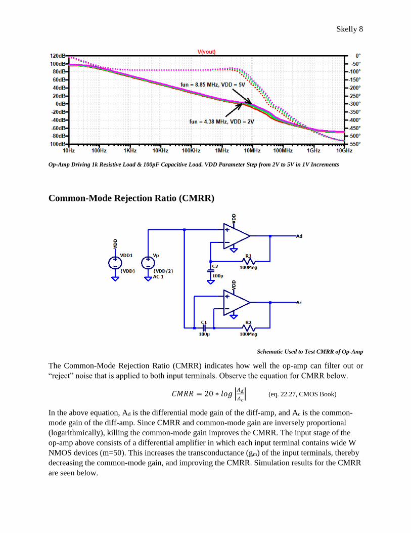
Skelly 8
Op-Amp Driving 1k Resistive Load & 100pF Capacitive Load. VDD Parameter Step from 2V to 5V in 1V Increments
Common-Mode Rejection Ratio (CMRR)
Schematic Used to Test CMRR of Op-Amp
The Common-Mode Rejection Ratio (CMRR) indicates how well the op-amp can filter out or
“reject” noise that is applied to both input terminals. Observe the equation for CMRR below.
𝐶𝑀𝑅𝑅 = 20 ∗ 𝑙𝑜𝑔 |𝐴𝑑
𝐴𝑐| (eq. 22.27, CMOS Book)
In the above equation, Ad is the differential mode gain of the diff-amp, and Ac is the common-
mode gain of the diff-amp. Since CMRR and common-mode gain are inversely proportional
(logarithmically), killing the common-mode gain improves the CMRR. The input stage of the
op-amp above consists of a differential amplifier in which each input terminal contains wide W
NMOS devices (m=50). This increases the transconductance (gm) of the input terminals, thereby
decreasing the common-mode gain, and improving the CMRR. Simulation results for the CMRR
are seen below.

Skelly 9
CMRR Simulation for Op-Amp Driving 100pF Capacitive Load. VDD Parameter Step from 2V to 5V in 1V Increments
CMRR Simulation for Op-Amp Driving 1k Resistive Load. VDD Parameter Step from 2V to 5V in 1V Increments
Power Supply Rejection Ratio (PSRR)
Schematic used to test positive PSRR of Op-Amp
The Power Supply Rejection Ratio (PSRR) defines how well an op-amp can reject noise on the
VDD or ground power buses. The larger the PSRR, the better the op-amp rejects noise on these
power buses. In the design of this op-amp, a compensation capacitor was connected from the
output back to the PMOS devices in the folded-cascode in order to filter out noise and improve
the positive PSRR. Simulation results for the positive and negative PSRR are seen below.

Skelly 10
PSRR+
PSRR+ Simulation for Op-Amp with no load. VDD Parameter Step from 2V to 5V in 1V Increments
PSRR-
Schematic used to test negative PSRR of Op-Amp
PSRR- Simulation for Op-Amp with no load. VDD Parameter Step from 2V to 5V in 1V Increments

Skelly 11
Step Response (VDD = 5V)
Unity follower configuration to test step response, rise time, fall time
Step Response of Op-Amp with VDD = 5V, Driving maximum load
Correcting the step response of the op-amp required important design decisions and
consideration of tradeoffs. The class AB amplifier used to drive the output signal is a good
example. Designing the output stage with wide W (m = 50) drastically increases the power
consumption of the op-amp. However, while having smaller W devices on the output stage may
conserve power, the step response becomes slow and unstable. Observe the rising edge of the
output signal below.
Zoomed-In View of Step Response to measure rise time

Skelly 12
The rise time of the output signal can be calculated by
𝑡𝑟𝑖𝑠𝑒 = 𝑡(90%) − 𝑡(10%) = 30.22µ𝑠 − 30.04µ𝑠
𝑡𝑟𝑖𝑠𝑒 = 0.18µ𝑠 = 180 𝑛𝑠
Zoomed-In View of Step Response to measure fall time.
The fall time of the output signal can be calculated by
𝑡𝑓𝑎𝑙𝑙 = 𝑡(10%) − 𝑡(90%) = 130.41µ𝑠 − 130.08µ𝑠
𝑡𝑓𝑎𝑙𝑙 = 0.33µ𝑠 = 330 𝑛𝑠
Step Response (VDD = 2V)
Unity follower configuration to test step response, rise time, fall time.
The same configuration was used to test the step response of the op-amp when the power supply
voltage is 2V. Simulation results are seen below.

Skelly 13
Step Response of Op-Amp with VDD = 2V, driving max load
Zoomed-In View of Step Response to measure rise time.
𝑡𝑟𝑖𝑠𝑒 = 30.30µ𝑠 − 30.06µ𝑠 = 0.24µ𝑠 = 240 𝑛𝑠
Zoomed-In View of Step Response to measure fall time.
𝑡𝑓𝑎𝑙𝑙 = 90.54µ𝑠 − 90.09µ𝑠 = 0.45µ𝑠 = 450 𝑛𝑠
Skelly 14
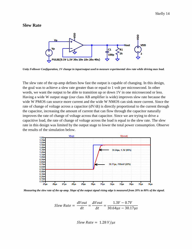
Slew Rate
Unity Follower Configuration, 1V change in input/output used to measure experimental slew rate while driving max load.
The slew rate of the op-amp defines how fast the output is capable of changing. In this design,
the goal was to achieve a slew rate greater than or equal to 1 volt per microsecond. In other
words, we want the output to be able to transition up or down 1V in one microsecond or less.
Having a wide W output stage (our class AB amplifier is wide) improves slew rate because the
wide W PMOS can source more current and the wide W NMOS can sink more current. Since the
rate of change of voltage across a capacitor (dV/dt) is directly proportional to the current through
the capacitor, increasing the amount of current that can flow through the capacitor naturally
improves the rate of change of voltage across that capacitor. Since we are trying to drive a
capacitive load, the rate of change of voltage across the load is equal to the slew rate. The slew
rate in this design was limited by the output stage to lower the total power consumption. Observe
the results of the simulation below.
Measuring the slew rate of the op-amp. Slope of the output signal rising edge is measured from 20% to 80% of the signal.
𝑆𝑙𝑒𝑤 𝑅𝑎𝑡𝑒 = 𝑑𝑉𝑜𝑢𝑡
𝑑𝑡=
𝛥𝑉𝑜𝑢𝑡
𝛥𝑡=
1.3𝑉 − 0.7𝑉
30.64µ𝑠 − 30.17µ𝑠
𝑆𝑙𝑒𝑤 𝑅𝑎𝑡𝑒 = 1.28 𝑉/µ𝑠

Skelly 15
Inverting Op-Amp Topology (VDD = 5V)
Schematic used to test operation of op-amp in the inverting topology with a gain of -10, VDD = 5V.
For the inverting op-amp topology, we know that the gain is equal to -1 multiplied by the ratio of
R2 divided by R1, or
𝑉𝑜𝑢𝑡
𝑉𝑖𝑛= −
𝑅2
𝑅1
Since R2 is ten times larger than R1 in the circuit above, the gain is -10. With a gain of -10 and
an input signal of 100mV oscillating around the common-mode voltage (2.5V), we expect an
output signal of 1V oscillating around the common-mode voltage, with a phase shift of 180˚.
Transient analysis of inverting op-amp with gain of -10, frequency of 1kHz.
The simulation results shown above confirm that the op-amp is working properly in the non-
inverting configuration with a gain of -10 for VDD = 5V.

Skelly 16
Inverting Op-Amp Topology (VDD = 2V)
Schematic used to test operation of op-amp in the inverting topology with a gain of -5, VDD = 2V.
Here, we test to make sure that the op-amp can operate down to VDD = 2V. To avoid clipping,
the gain has been changed in this configuration to better suit VDD = 2V.
Since R2 is five times larger than R1 in the circuit above, the gain is -5. With a gain of -5 and an
input signal of 100mV oscillating around the common-mode voltage (1V), we expect an output
signal of 500mV oscillating around the common-mode voltage, with a phase shift of 180˚.
Transient analysis of inverting op-amp with gain of -5, frequency of 1kHz.
The simulation results shown above confirm that the op-amp is working properly in the non-
inverting configuration with a gain of -5 for VDD = 2V.

Skelly 17
Power Dissipation (No Load)
The power dissipated by the op-amp can be estimated by summing the currents in each branch
(in the biasing circuit as well as the op-amp) and multiplying the sum by the power supply
voltage (VDD).
In the biasing circuit, there are 10 total branches, each with 10µA of current flowing. In the op-
amp, there are 7 total branches, 6 of which have 10µA of current flowing, and 1 which has
500µA of current flowing (output stage, W is 50 times larger). This means we can approximate
the power dissipated by the op-amp as
𝑃 = 𝐼𝑉 = [(16 ∗ 10µ𝐴) + ∗ 500µ𝐴] ∗ 𝑉𝐷𝐷
𝑃 = 660µ𝐴 ∗ 𝑉𝐷𝐷
Schematic drafted to measure current drawn from power supply at different power supply voltages.
Transient simulation showing power consumed by op-amp at different power supply voltages.
For all values of VDD, the op-amp consumes less than 7mW of power.

Skelly 18
Operation as Temperature Changes
Adding a temperature coefficient of TCR = 0.002 to the resistor in the BMR and the zero-nulling
resistor in the op-amp, we can observe the operation of the op-amp at temperatures above and
below nominal operating temperature.
Frequency Response
Frequency response for op-amp driving resistive and capacitive load, temperature stepping from 0˚C to 200˚C. VDD = 5V
Since the temperature coefficient of the resistor is positive, its resistance will increase with
increasing temperature. As the resistance of the resistor in the beta multiplier reference increases,
the reference current, and as a result also the reference voltages, of the BMR decrease. This will
cause a chain reaction, as the bias voltages generated by the biasing circuit will then be
inaccurate, matching will be poor, and the op-amp will begin to perform poorly. For example, in
the frequency response above, as the temperature increases, the unity gain frequency of the op-
amp decreases considerably. Consider also the step response shown below. As temperature rises,
the step response slowly becomes unstable, and the output rings with some slight overshoot.
Even at temperatures lower than room temperature shown below, the op-amp’s step response
looks less like a first order response than it does at room temperature or slightly above.
Step Response
Step response for op-amp driving max load. Ringing becomes obvious at 200˚C.

Skelly 19
Summary
The op-amp design described in this report meets all of the project specifications. The DC open-
loop gain (AOLDC) of the op-amp is 96.1 dB at the lowest power supply voltage (VDD = 2V)
driving the minimum load (1k resistive) and 106.2 dB at the highest power supply voltage (VDD
= 5V) driving the maximum load (100pF capacitive). The unity gain frequency, or gain-
bandwidth product (GBW), is 3.65 MHz at the lowest power supply voltage driving the
minimum load, and 8.45 MHz at the highest power supply voltage driving the maximum load.
The common-mode voltage (input CMR) of the op-amp can range from 850 mV (CMRMIN) up to
voltages 650 mV above the power supply voltage (CMRMAX). For operation in the saturation
region, the output can swing within 50 mV of the power supply rails (down to 50 mV, up to
VDD – 50 mV). The op-amp output can go all the way up to VDD and all the way down to
ground, but the output stage transistors will be operating in the triode region.
With no load, the op-amp dissipates 6.84 mW of power at the maximum power supply voltage of
5V, and dissipates 1.53 mW at the minimum power supply voltage of 2V. Dividing out the
power supply voltage, this translates to 1.37 mA of current drawn at VDD = 5V, and 765 µA of
current drawn at VDD = 2V.
Key design decisions, coupled with considerable tradeoffs, were made regarding input stage
MOSFET widths, output stage MOSFET widths, compensation capacitor size, and bias current.
• Input Stage MOSFET Widths: Using a large multiplier (m=50) on the input terminals
of the op-amp allows for a better common-mode rejection ratio. However, it greatly
increases the layout size of the differential amplifier. It was decided that the CMRR
improvement was more important in this case than minimizing layout size.
• Output Stage MOSFET Widths: Using a large multiplier (m=50) on the transistors that
make up the output buffer allows for better slew rate, faster rise time and fall time of
output signals, and more capability for driving larger loads. However, much like the input
stage, these wider W devices take up much more layout space, and also source/sink much
more current, which causes the op-amp to consume much more power. The op-amp
power consumption could be greatly reduced by using a smaller multiplier in the output
stage, but this would cause the slew rate to decrease, and the step response to overshoot.
• Compensation Capacitor Size: Using a 13pF compensation capacitor allowed for the
maximum power supply rejection ratio, and the cleanest step response. However, a 13pF
capacitor is large for an on-chip capacitor, and would take up a significant amount of
layout space. The PSRR could also be improved by increasing the width of the output
stage MOSFETs, but as was discussed previously, increasing these widths greatly
increases the power consumption of the op-amp. For this design, is was decided that the
larger compensation capacitor was a worthwhile tradeoff to reduce power consumption
and maintain a clean step response.

Skelly 20
• Bias Current: The bias current in this design was selected to be 10µA. Lower current
translates to higher gain, and using 10µA makes calculations much simpler. However,
using a drain current as low as 10µA requires the output stage to be larger in order to
achieve a reasonably fast slew rate, and ultimately results in more power consumption as
a result. It was decided that using a large enough output stage to meet the slew rate
requirement would be necessary regardless of drain current, since the drain current is
much smaller than the current that is sourced/sunk in the output buffer.
Future Work and Improvement
Although the op-amp meets the specifications for this project, there are certainly areas where the
design can be improved. The key areas where the op-amp can be improved are input CMR, gain
bandwidth product (unity gain frequency), phase margin for capacitive loads, power
consumption, slew rate, and operation with changing temperature.
• Input CMR and Gain Bandwidth Product: In this design, the input stage of the op-
amp consists of an NMOS differential amplifier, with a CMR that can extend up to 650
mV above VDD and down to 850 mV. However, this CMR can be greatly improved by
adding a PMOS differential amplifier stage to the input. This stage would require more
hardware (two more PMOS devices to source current, two more PMOS devices as part of
the differential pair, and two more NMOS devices to sink current), and would increase
the power consumption of the circuit slightly, along with increasing the layout size.
However, by adding the PMOS diff-amp, the common-mode range would extend above
VDD still, and also below ground. When the input common-mode voltage is high and
moves toward VDD, this would shut off the PMOS diff-amp input transistors, but the
NMOS diff-amp inputs would still be on. When the input common-mode voltage is low
and moves toward ground, this would shut off the NMOS diff-amp input transistors, but
the PMOS diff-amp inputs would still be on. Further, when both the NMOS and PMOS
diff-amps are on, the input stage transconductance would be the sum of the
transconductances of each, and would move the unity gain frequency out. The addition of
the PMOS diff-amp to the input stage would certainly improve the performance of the
op-amp.
• Phase Margin for Capacitive Loads: The op-amp’s phase margin for resistive loads and
for no loads is close to optimal (90˚). However, for capacitive loads, the phase margin is
much lower, and far from optimal. If this chip were to be fabricated, it is likely that the
op-amp would not be stable for capacitive loads, and certainly would not be able to drive
the capacitance of the oscilloscope for testing. In simulation, all is well with the step
response, but many conditions in simulation, even of a realistic design in a small process,

Skelly 21
are ideal. For quality performance, the design would need to be improved to have a
higher phase margin for capacitive loads.
• Power Consumption: The power consumed by the op-amp in this design can be
improved only slightly by using a smaller bias current. The power consumption can
greatly be improved by making the output stage smaller, but this will lead to other issues,
such as slew rate becoming slower, and step response ringing.
• Slew Rate: The design meets the specification for slew rate, but only by a couple
hundred millivolts for VDD = 2V. If minimizing power consumption is not essential, the
output stage could be designed to source and sink much larger amounts of current, which
would make it capable of driving large loads. The slew rate, as a result, would improve
substantially. In this design, the output stage was designed for optimal slew rate along
with optimal power consumption in mind. Future designs that do not require low power
constraints to be met could drive large loads with no problem at the cost of power, and
larger layout size.
• Operation with Changes in Temperature: From the simulation results, we can see that
at high temperatures, the op-amp performance is less desirable. In future designs, a
bandgap voltage reference could be used to bias the op-amp MOSFETs to improve
performance at temperatures higher and lower than room temperature. The bandgap
voltage reference is capable of outputting voltages that change very little with large
changes in temperature and large changes in power supply voltage. Using a bandgap
reference for biasing would eliminate the ringing in the step response at high
temperatures, and would also improve the unity gain frequency at high temperatures.