iwr6843, iwr6443 single-chip 60- to 64-ghz mmwave sensor
TRANSCRIPT

IWR6843, IWR6443 Single-Chip 60- to 64-GHz mmWave Sensor
1 Features• FMCW transceiver
– Integrated PLL, transmitter, receiver, Baseband, and ADC
– 60- to 64-GHz coverage with 4-GHz continuous bandwidth
– Four receive channels– Three transmit channels– Supports 6-bit phase shifter for TX Beam
forming– Ultra-accurate chirp engine based on fractional-
N PLL– TX power: 12 dBm– RX noise figure:
• 12 dB– Phase noise at 1 MHz:
• –93 dBc/Hz• Built-in calibration and self-test
– Arm® Cortex®-R4F-based radio control system– Built-in firmware (ROM)– Self-calibrating system across frequency and
temperature– Embedded self-monitoring with no host
processor involvement on Functional Safety-Compliant devices
• C674x DSP for advanced signal processing (IWR6843 only)
• Hardware accelerator for FFT, filtering, and CFAR processing
• Memory compression• Arm-R4F microcontroller for object detection, and
interface control– Supports autonomous mode (loading user
application from QSPI flash memory)• Internal memory with ECC
– IWR6843: 1.75 MB, divided into MSS program RAM (512 KB), MSS data RAM (192 KB), DSP L1 RAM (64KB) and L2 RAM (256 KB), and L3 radar data cube RAM (768 KB)
– IWR6443: 1.4 MB, divided into MSS program RAM (512 KB), MSS data RAM (192 KB), and L3 radar data cube RAM (768 KB)
– Technical reference manual includes allowed size modifications
• Other interfaces available to user application– Up to 6 ADC channels (low sample rate
monitoring)– Up to 2 SPI ports– Up to 2 UARTs– 1 CAN-FD interface– I2C– GPIOs– 2 lane LVDS interface for raw ADC data and
debug instrumentation• Functional Safety-Compliant
– Developed for functional safety applications– Documentation available to aid IEC 61508
functional safety system design up to SIL 3– Hardware integrity up to SIL-2– Safety-related certification
• IEC 61508 certified upto SIL 2 by TUV SUD• Non-Functional safety variants also available• Power management
– Built-in LDO network for enhanced PSRR– I/Os support dual voltage 3.3 V/1.8 V
• Clock source– 40.0 MHz crystal with internal oscillator– Supports external oscillator at 40 MHz– Supports externally driven clock (square/sine)
at 40 MHz• Easy hardware design
– 0.65-mm pitch, 161-pin 10.4 mm × 10.4 mm flip chip BGA package for easy assembly and low-cost PCB design
– Small solution size• Operating conditions:
– Junction temperature range of –40°C to 105°C
IWR6843, IWR6443SWRS219E – OCTOBER 2018 – REVISED JUNE 2021
An IMPORTANT NOTICE at the end of this data sheet addresses availability, warranty, changes, use in safety-critical applications, intellectual property matters and other important disclaimers. PRODUCTION DATA.
2 Applications• Industrial sensor for measuring range, velocity, and
angle• Building automation• Displacement sensing• Gesture recognition• Robotics
• Traffic monitoring• Proximity and position sensing• Security and surveillance• Factory automation safety guards• People counting• Motion detection• Occupancy detection
3 DescriptionThe IWR6x43 device is an integrated single chip mmWave sensor based on FMCW radar technology capable of operation in the 60-GHz to 64-GHz band. It is built with TI’s low power 45-nm RFCMOS process and enables unprecedented levels of integration in an extremely small form factor. This device is an ideal solution for low power, self-monitored, ultra-accurate radar systems in the industrial space. Multiple variants are currently available including Functional Safety-Compliant devices and non-functional safety devices.
Device InformationPART NUMBER(2) PACKAGE(1) BODY SIZE TRAY / TAPE AND REEL
IWR6843AQGABL FCBGA (161) 10.4 mm × 10.4 mm Tray
IWR6843AQGABLR FCBGA (161) 10.4 mm × 10.4 mm Tape and Reel
IWR6843AQSABL FCBGA (161) 10.4 mm × 10.4 mm Tray
IWR6843AQSABLR FCBGA (161) 10.4 mm × 10.4 mm Tape and Reel
IWR6843ABGABL FCBGA (161) 10.4 mm × 10.4 mm Tray
IWR6843ABGABLR FCBGA (161) 10.4 mm × 10.4 mm Tape and Reel
IWR6843ABSABL FCBGA (161) 10.4 mm × 10.4 mm Tray
IWR6843ABSABLR FCBGA (161) 10.4 mm × 10.4 mm Tape and Reel
IWR6443AQGABL FCBGA (161) 10.4 mm × 10.4 mm Tray
IWR6443AQGABLR FCBGA (161) 10.4 mm × 10.4 mm Tape and Reel
(1) For more information, see Section 13, Mechanical, Packaging, and Orderable Information.(2) For more information, see Section 12.1, Device Nomenclature.
IWR6843, IWR6443SWRS219E – OCTOBER 2018 – REVISED JUNE 2021 www.ti.com
2 Submit Document Feedback Copyright © 2021 Texas Instruments Incorporated
Product Folder Links: IWR6843 IWR6443

4 Functional Block DiagramFigure 4-1 shows the functional block diagram of the device.
IF ADC
Digital
Front-End
(Decimation
Filter Chain)
LNA
IF ADCLNA
IF ADCLNA
IF ADCLNA
PA ´Å
PA ´ÅSynth
(20 GHz)
Ramp
Generatorx3
Osc.
Radio (BIST)
Processor
(For RF Calibration
& Self-Test ±�TI
Programmed)
Prog RAM & ROM
Data RAM
GPADC
Temp
Cortex R4F
@ 200MHz
(User Programmable)
Prog RAM(512kB)
Data RAM(192kB)
Boot ROM
QSPI
SPI
SPI / I2C
UARTs
DMA
Test/
DebugADC
Buffer
LVDS
RF/Analog Sub-System
Radio Processor
Sub-System(TI Programmed)
Main Sub-System(Customer Programmed)
Serial Flash Interface
Optional External
MCU Interface
PMIC Control
CAN-FD Communication
JTAG For Debug/
Development
High-Speed ADC Output
Interface (For Recording)
6
CAN-FD
DSP Sub-System(Customer Programmed)
Mailbox
Bus M
atr
ix
HILHigh-Speed Input For
Hardware-In-Loop Verification
C674x DSP
@ 600 MHz
(IWR6843 ONLY)
L1P (32kB)
L1D (32kB)
L2 (256kB)
DMA CRCRadar Data Memory
768 kB
PA ´Å
Radar Hardware Accelerator
(FFT, Log Mag, And Others)
Figure 4-1. Functional Block Diagram
www.ti.comIWR6843, IWR6443
SWRS219E – OCTOBER 2018 – REVISED JUNE 2021
Copyright © 2021 Texas Instruments Incorporated Submit Document Feedback 3
Product Folder Links: IWR6843 IWR6443

Table of Contents1 Features............................................................................12 Applications..................................................................... 23 Description.......................................................................24 Functional Block Diagram.............................................. 35 Revision History.............................................................. 56 Device Comparison......................................................... 6
6.1 Related Products........................................................ 77 Terminal Configuration and Functions..........................8
7.1 Pin Diagram................................................................ 87.2 Signal Descriptions................................................... 127.3 Pin Attributes.............................................................17
8 Specifications................................................................ 258.1 Absolute Maximum Ratings...................................... 258.2 ESD Ratings............................................................. 258.3 Power-On Hours (POH)............................................ 268.4 Recommended Operating Conditions.......................278.5 Power Supply Specifications.....................................288.6 Power Consumption Summary................................. 298.7 RF Specification........................................................308.8 CPU Specifications................................................... 318.9 Thermal Resistance Characteristics for FCBGA
Package [ABL0161].....................................................328.10 Timing and Switching Characteristics..................... 32
9 Detailed Description......................................................569.1 Overview................................................................... 569.2 Functional Block Diagram......................................... 569.3 Subsystems.............................................................. 579.4 Other Subsystems.................................................... 61
10 Monitoring and Diagnostics....................................... 6310.1 Monitoring and Diagnostic Mechanisms................. 63
11 Applications, Implementation, and Layout............... 6811.1 Application Information............................................6811.2 Reference Schematic..............................................68
12 Device and Documentation Support..........................6912.1 Device Nomenclature..............................................6912.2 Tools and Software................................................. 7012.3 Documentation Support.......................................... 7012.4 Support Resources................................................. 7012.5 Trademarks.............................................................7112.6 Electrostatic Discharge Caution..............................7112.7 Glossary..................................................................71
13 Mechanical, Packaging, and Orderable Information.................................................................... 7213.1 Packaging Information............................................ 7213.2 Tray Information for ABL, 10.4 × 10.4 mm .............76
IWR6843, IWR6443SWRS219E – OCTOBER 2018 – REVISED JUNE 2021 www.ti.com
4 Submit Document Feedback Copyright © 2021 Texas Instruments Incorporated
Product Folder Links: IWR6843 IWR6443
5 Revision HistoryChanges from October 1, 2020 to June 30, 2021 (from Revision D (Oct 2020) to Revision E (June 2021)) Page• Global: Updated to reflect Functional Safety-Compliance.................................................................................. 1• Global: Updated/Changed Master Subsystem to Main Subsystem and Master R4F to MSS R4F.................... 1• Global: Updated/Changed A2D to ADC..............................................................................................................1• (Features) : Updated Functional-Safety Compliance Certification Collateral..................................................... 1• (Device Information) : Added additional Secure production parts for IWR6843................................................. 2• Updated/Changed Functional Block Diagram ....................................................................................................3• (Device Comparison):Updated/Changed SIL row to reflect Functional Safety-Compliance for IWR6843..........6• (Device Comparison): Added a table-note about LVDS and Non-Functional Safety Variant Information...........6• (Device Comparison): Updated/Changed the IWR6843AOP Product status from "AI" to "PD" .........................6• (Absolute Maximum Ratings): Added entries for externally supplied power on the RF inputs (TX and RX) and
a table-note for the signal level applied on TX..................................................................................................25• (ESD Ratings): Changed HBM ESD value from ±1000 V to ±2000 V, CDM ESD value from ±250 V to ±500 V
and added footnote about corner pins.............................................................................................................. 25• Transmit Subsystem (Per Channel): Updated/Changed figure.........................................................................59• Updated/changed "Master" to "Main" in Processor Subsystem image.............................................................60• (Monitoring and Diagnostic Mechanisms): Updated/Changed table header and description to reflect
Functional Safety-Compliance..........................................................................................................................63• (Monitoring and Diagnostic Mechanisms): Updated/Changed Master R4F to MSS R4F and Master SS to
Main SS............................................................................................................................................................ 63• (Device Nomenclature):Updated/changed figure to reflect Functional Safety-Compliance, SIL 2 for Safety
Level B..............................................................................................................................................................69• (Tray Information for ABL, 10.4 × 10.4 mm): Added tray information for secure parts..................................... 76
www.ti.comIWR6843, IWR6443
SWRS219E – OCTOBER 2018 – REVISED JUNE 2021
Copyright © 2021 Texas Instruments Incorporated Submit Document Feedback 5
Product Folder Links: IWR6843 IWR6443
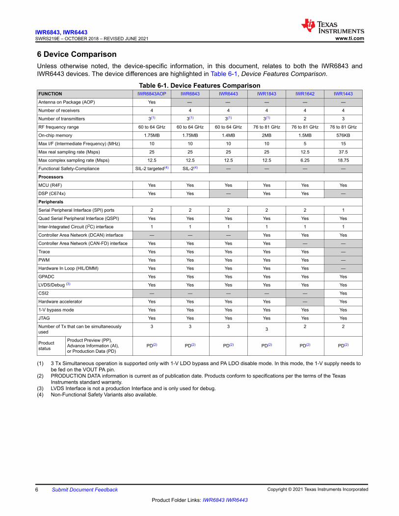
6 Device ComparisonUnless otherwise noted, the device-specific information, in this document, relates to both the IWR6843 and IWR6443 devices. The device differences are highlighted in Table 6-1, Device Features Comparison.
Table 6-1. Device Features ComparisonFUNCTION IWR6843AOP IWR6843 IWR6443 IWR1843 IWR1642 IWR1443
Antenna on Package (AOP) Yes — — — — —
Number of receivers 4 4 4 4 4 4
Number of transmitters 3(1) 3(1) 3(1) 3(1) 2 3
RF frequency range 60 to 64 GHz 60 to 64 GHz 60 to 64 GHz 76 to 81 GHz 76 to 81 GHz 76 to 81 GHz
On-chip memory 1.75MB 1.75MB 1.4MB 2MB 1.5MB 576KB
Max I/F (Intermediate Frequency) (MHz) 10 10 10 10 5 15
Max real sampling rate (Msps) 25 25 25 25 12.5 37.5
Max complex sampling rate (Msps) 12.5 12.5 12.5 12.5 6.25 18.75
Functional Safety-Compliance SIL-2 targeted(4) SIL-2(4) — — — —
Processors
MCU (R4F) Yes Yes Yes Yes Yes Yes
DSP (C674x) Yes Yes — Yes Yes —
Peripherals
Serial Peripheral Interface (SPI) ports 2 2 2 2 2 1
Quad Serial Peripheral Interface (QSPI) Yes Yes Yes Yes Yes Yes
Inter-Integrated Circuit (I2C) interface 1 1 1 1 1 1
Controller Area Network (DCAN) interface — — — Yes Yes Yes
Controller Area Network (CAN-FD) interface Yes Yes Yes Yes — —
Trace Yes Yes Yes Yes Yes —
PWM Yes Yes Yes Yes Yes —
Hardware In Loop (HIL/DMM) Yes Yes Yes Yes Yes —
GPADC Yes Yes Yes Yes Yes Yes
LVDS/Debug (3) Yes Yes Yes Yes Yes Yes
CSI2 — — — — — Yes
Hardware accelerator Yes Yes Yes Yes — Yes
1-V bypass mode Yes Yes Yes Yes Yes Yes
JTAG Yes Yes Yes Yes Yes Yes
Number of Tx that can be simultaneously used
3 3 3 3 2 2
Product status
Product Preview (PP),Advance Information (AI),or Production Data (PD)
PD(2) PD(2) PD(2) PD(2) PD(2) PD(2)
(1) 3 Tx Simultaneous operation is supported only with 1-V LDO bypass and PA LDO disable mode. In this mode, the 1-V supply needs to be fed on the VOUT PA pin.
(2) PRODUCTION DATA information is current as of publication date. Products conform to specifications per the terms of the Texas Instruments standard warranty.
(3) LVDS Interface is not a production Interface and is only used for debug.(4) Non-Functional Safety Variants also available.
IWR6843, IWR6443SWRS219E – OCTOBER 2018 – REVISED JUNE 2021 www.ti.com
6 Submit Document Feedback Copyright © 2021 Texas Instruments Incorporated
Product Folder Links: IWR6843 IWR6443

6.1 Related ProductsFor information about other devices in this family of products or related products see the links that follow.
mmWave sensors TI’s mmWave sensors rapidly and accurately sense range, angle and velocity with less power using the smallest footprint mmWave sensor portfolio for industrial applications.
mmWave IWR The Texas Instruments IWRxxxx family of mmWave Sensors are highly integrated and built on RFCMOS technology operating in 76- to 81-GHz or 60- to 64-GHz frequency band. The devices have a closed-loop PLL for precise and linear chirp synthesis, includes a built-in radio processor (BIST) for RF calibration and safety monitoring. The devices have a very small-form factor, low power consumption, and are highly accurate. Industrial applications from long range to ultra short range can be realized using these devices.
Companion products for IWR6843
Review products that are frequently purchased or used in conjunction with this product.
Reference designs for IWR6843
The IWR6843 TI Designs Reference Design Library is a robust reference design library spanning analog, embedded processor and connectivity. Created by TI experts to help you jump-start your system design, all TI Designs include schematic or block diagrams, BOMs, and design files to speed your time to market. Search and download designs at ti.com/tidesigns.
www.ti.comIWR6843, IWR6443
SWRS219E – OCTOBER 2018 – REVISED JUNE 2021
Copyright © 2021 Texas Instruments Incorporated Submit Document Feedback 7
Product Folder Links: IWR6843 IWR6443

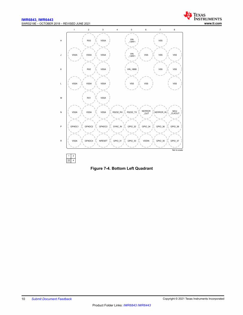
7 Terminal Configuration and Functions7.1 Pin DiagramFigure 7-1 shows the pin locations for the 161-pin FCBGA package. Figure 7-2, Figure 7-3, Figure 7-4, and Figure 7-5 show the same pins, but split into four quadrants.
1 2 3 4 5 6 7 8 9 10 11 12 13 14 15
A
B
C
D
E
F
G
H
J
K
L
M
N
P
R
Not to scale
VSSA VOUT_PA VSSA VSSA VSSA VSSA VOUT_14APLL
VSSA OSC_CLKOUT
VSSA
VSSA VOUT_PA VSSA TX1 VSSA TX2 VSSA VSSA VBGAPVIN
_18CLKVIN
_18VCOVSSA CLKP
VSSAVIN
_13RF2VSSA VSSA VSSA VSSA VSSA VSSA VSSA GPADC5 VSSA CLKM
VIN_13RF2
SPIA_MOSI GPADC6
VSSA VSSA VSSA VSS VSS VSS VSS VSS SPIA_CLK SPIA_MISO
RX4 VSSA VIN_18BB VSS VSS SPIB_MOSI VIOIN
VSSA VSSA VSSAVIN
_13RF1VSS VSS VSS VSS SYNC_OUT SPIB_MISO VIN_SRAM
RX3 VSSAVIN
_13RF1VSS VSS VSS GPIO_0 SPIB_CS_N VDDIN
VSSA VSSA VSSAVIN
_13RF1VSS VSS VSS VSS GPIO_1 LVDS_TXP[0] LVDS_TXM[0]
RX2 VSSA VIN_18BB VSS VSS VSS VSS VSS GPIO_2 LVDS_TXP[1] LVDS_TXM[1]
VSSA VSSA VSSA VSS VSS VSS VSS VPP LVDS_CLKP LVDS_CLKM
RX1 VSSALVDS
_FRCLKPLVDS
_FRCLKM
VSSA VSSA VSSA RS232_RX RS232_TX NERROR_INMCU
_CLKOUTWARM
_RESETTMS VDDIN QSPI[1] TDO DMM_SYNC GPIO_47
GPADC1 GPADC2 GPADC3 SYNC_IN GPIO_32 GPIO_34 GPIO_36 GPIO_38PMIC
_CLKOUTTCK QSPI_CS_N QSPI[3] VNWA VDDIN
VSSA GPADC4 NRESET GPIO_31 GPIO_33 VDDIN GPIO_35 GPIO_37 VIOIN_18 VIOIN TDI QSPI_CLK QSPI[0] QSPI[2] VSS
VOUT_14SYNTH_18VCO
VIOIN_18DIFF
SPIA_CS_N
SPIB_CLK
SPI_HOST_INTR
TX3
NERROR_OUT
Figure 7-1. Pin Diagram
IWR6843, IWR6443SWRS219E – OCTOBER 2018 – REVISED JUNE 2021 www.ti.com
8 Submit Document Feedback Copyright © 2021 Texas Instruments Incorporated
Product Folder Links: IWR6843 IWR6443

1 2 3 4 5 6 7 8
A
B
C
D
E
F
G
Not to scale
VSSA VOUT_PA VSSA VSSA VSSA
VSSA VOUT_PA VSSA TX1 VSSA TX2 VSSA TX3
VSSAVIN
_13RF2VSSA VSSA VSSA VSSA VSSA VSSA
VIN_13RF2
VSSA VSSA VSSA VSS VSS VSS
RX4 VSSA VIN_18BB
VSSA VSSA VSSAVIN
_13RF1VSS VSS VSS
1
3
2
4
Figure 7-2. Top Left Quadrant
9 10 11 12 13 14 15
A
B
C
D
E
F
G
Not to scale
VSSAVOUT
_14APLLVSSA
OSC
_CLKOUTVSSA
VSSA VBGAPVIN
_18CLK
VIN
_18VCOVSSA CLKP
VSSA VSSA CLKM
SPIA_MOSI
VSS VSS SPIA_CLK SPIA_MISO SPIA_CS_N
VSS VSS SPIB_MOSI SPIB_CLK VIOIN
VSS SYNC_OUT SPIB_MISO VIN_SRAM
1
3
2
4
VIOIN_18DIFF
VOUT
_14SYNTH
GPADC5
GPADC6
Figure 7-3. Top Right Quadrant
www.ti.comIWR6843, IWR6443
SWRS219E – OCTOBER 2018 – REVISED JUNE 2021
Copyright © 2021 Texas Instruments Incorporated Submit Document Feedback 9
Product Folder Links: IWR6843 IWR6443
1 2 3 4 5 6 7 8
H
J
K
L
M
N
P
R
Not to scale
RX3 VSSAVIN
_13RF1VSS
VSSA VSSA VSSAVIN
_13RF1VSS VSS VSS
RX2 VSSA VIN_18BB VSS VSS
VSSA VSSA VSSA VSS VSS VSS
RX1 VSSA
VSSA VSSA VSSA RS232_RX RS232_TXNERROR
_OUTNERROR_IN
MCU_CLKOUT
GPADC1 GPADC2 GPADC3 SYNC_IN GPIO_32 GPIO_34 GPIO_36 GPIO_38
VSSA GPADC4 NRESET GPIO_31 GPIO_33 VDDIN GPIO_35 GPIO_37
1
3
2
4
Figure 7-4. Bottom Left Quadrant
IWR6843, IWR6443SWRS219E – OCTOBER 2018 – REVISED JUNE 2021 www.ti.com
10 Submit Document Feedback Copyright © 2021 Texas Instruments Incorporated
Product Folder Links: IWR6843 IWR6443

9 10 11 12 13 14 15
H
J
K
L
M
N
P
R
Not to scale
VSS VSS GPIO_0 SPIB_CS_N VDDIN
VSS GPIO_1 LVDS_TXP[0] LVDS_TXM[0]
VSS VSS VSS GPIO_2 LVDS_TXP[1] LVDS_TXM[1]
VSS VPP LVDS_CLKP LVDS_CLKM
LVDS_FRCLKP
LVDS_FRCLKM
WARM_RESET
TMS VDDIN QSPI[1] TDO DMM_SYNC GPIO_47
PMIC_CLKOUT
TCK QSPI_CS_N QSPI[3] VNWA VDDIN
VIOIN_18 VIOIN TDI QSPI_clk QSPI[0] QSPI[2] VSS
1
3
2
4
SPI_HOST_INTR_1
Figure 7-5. Bottom Right Quadrant
www.ti.comIWR6843, IWR6443
SWRS219E – OCTOBER 2018 – REVISED JUNE 2021
Copyright © 2021 Texas Instruments Incorporated Submit Document Feedback 11
Product Folder Links: IWR6843 IWR6443

7.2 Signal Descriptions
Note
All digital IO pins of the device (except NERROR IN, NERROR_OUT, and WARM_RESET) are non-failsafe; hence, care needs to be taken that they are not driven externally without the VIO supply being present to the device.
Note
The GPIO state during the power supply ramp is not ensured. In case the GPIO is used in the application where the state of the GPIO is critical, even when NRESET is low, a tri-state buffer should be used to isolate the GPIO output from the radar device and a pull resister used to define the required state in the application. The NRESET signal to the radar device could be used to control the output enable (OE) of the tri-state buffer.
7.2.1 Signal Descriptions - Digital
SIGNAL NAME PIN TYPE DESCRIPTION BALL NO.
BSS_UART_TX O Debug UART Transmit [Radar Block] F14, H14, K13, N10, N13, N4, N5, R8
CAN_FD_RX I CAN FD (MCAN) Receive Signal D13, F14, N10, N4, P12
CAN_FD_TX O CAN FD (MCAN) Transmit Signal E14, H14, N5, P10, R14
DMM0 I Debug Interface (Hardware In Loop) - Data Line R4
DMM1 I Debug Interface (Hardware In Loop) - Data Line P5
DMM2 I Debug Interface (Hardware In Loop) - Data Line R5
DMM3 I Debug Interface (Hardware In Loop) - Data Line P6
DMM4 I Debug Interface (Hardware In Loop) - Data Line R7
DMM5 I Debug Interface (Hardware In Loop) - Data Line P7
DMM6 I Debug Interface (Hardware In Loop) - Data Line R8
DMM7 I Debug Interface (Hardware In Loop) - Data Line P8
DMM_CLK I Debug Interface (Hardware In Loop) - Clock N15
DMM_MUX_IN I Debug Interface (Hardware In Loop) Mux Select between DMM1 and DMM2 (Two Instances) G13, J13, P4
DMM_SYNC I Debug Interface (Hardware In Loop) - Sync N14
DSS_UART_TX O Debug UART Transmit [DSP] D13, E13, G14, P8, R12
EPWM1A O PWM Module 1 - Output A N5, N8
EPWM1B O PWM Module 1 - Output B H13, N5, P9
EPWM1SYNCI I PWM Module 1 - Sync Input J13
EPWM2A O PWM Module 2- Output A H13, N4, N5, P9
EPWM2B O PWM Module 2 - Output B N4
EPWM2SYNCO O PWM Module 2 - Sync Output R7
EPWM3A O PWM Module 3 - Output A N4
EPWM3SYNCO O PWM Module 3 - Sync Output P6
GPIO_0 IO General-purpose I/O H13
GPIO_1 IO General-purpose I/O J13
GPIO_2 IO General-purpose I/O K13
GPIO_3 IO General-purpose I/O E13
GPIO_4 IO General-purpose I/O H14
GPIO_5 IO General-purpose I/O F14
GPIO_6 IO General-purpose I/O P11
IWR6843, IWR6443SWRS219E – OCTOBER 2018 – REVISED JUNE 2021 www.ti.com
12 Submit Document Feedback Copyright © 2021 Texas Instruments Incorporated
Product Folder Links: IWR6843 IWR6443

SIGNAL NAME PIN TYPE DESCRIPTION BALL NO.GPIO_7 IO General-purpose I/O R12
GPIO_8 IO General-purpose I/O R13
GPIO_9 IO General-purpose I/O N12
GPIO_10 IO General-purpose I/O R14
GPIO_11 IO General-purpose I/O P12
GPIO_12 IO General-purpose I/O P13
GPIO_13 IO General-purpose I/O H13
GPIO_14 IO General-purpose I/O N5
GPIO_15 IO General-purpose I/O N4
GPIO_16 IO General-purpose I/O J13
GPIO_17 IO General-purpose I/O P10
GPIO_18 IO General-purpose I/O N10
GPIO_19 IO General-purpose I/O D13
GPIO_20 IO General-purpose I/O E14
GPIO_21 IO General-purpose I/O F13
GPIO_22 IO General-purpose I/O G14
GPIO_23 IO General-purpose I/O R11
GPIO_24 IO General-purpose I/O N13
GPIO_25 IO General-purpose I/O N8
GPIO_26 IO General-purpose I/O K13
GPIO_27 IO General-purpose I/O P9
GPIO_28 IO General-purpose I/O P4
GPIO_29 IO General-purpose I/O G13
GPIO_30 IO General-purpose I/O C13
GPIO_31 IO General-purpose I/O R4
GPIO_32 IO General-purpose I/O P5
GPIO_33 IO General-purpose I/O R5
GPIO_34 IO General-purpose I/O P6
GPIO_35 IO General-purpose I/O R7
GPIO_36 IO General-purpose I/O P7
GPIO_37 IO General-purpose I/O R8
GPIO_38 IO General-purpose I/O P8
GPIO_47 IO General-purpose I/O N15
I2C_SCL IO I2C Clock G14, N4
I2C_SDA IO I2C Data F13, N5
LVDS_TXP[0] ODifferential data Out – Lane 0
J14
LVDS_TXM[0] O J15
LVDS_TXP[1] ODifferential data Out – Lane 1
K14
LVDS_TXM[1] O K15
LVDS_CLKP ODifferential clock Out
L14
LVDS_CLKM O L15
LVDS_FRCLKP ODifferential Frame Clock
M14
LVDS_FRCLKM O M15
MCU_CLKOUT O Programmable clock given out to external MCU or the processor N8
MSS_UARTA_RX I Main Subsystem - UART A Receive F14, N4, R11
MSS_UARTA_TX O Main Subsystem - UART A Transmit H14, N13, N5, R4
www.ti.comIWR6843, IWR6443
SWRS219E – OCTOBER 2018 – REVISED JUNE 2021
Copyright © 2021 Texas Instruments Incorporated Submit Document Feedback 13
Product Folder Links: IWR6843 IWR6443

SIGNAL NAME PIN TYPE DESCRIPTION BALL NO.MSS_UARTB_RX IO Main Subsystem - UART B Receive N4, P4
MSS_UARTB_TX O Main Subsystem - UART B Transmit F14, H14, K13, N13, N5, P10, P7
NDMM_EN I Debug Interface (Hardware In Loop) Enable - Active Low Signal N13, N5
NERROR_IN IFailsafe input to the device. Nerror output from any other device can be concentrated in the error signaling monitor module inside the device and appropriate action can be taken by Firmware
N7
NERROR_OUT OOpen drain fail safe output signal. Connected to PMIC/Processor/MCU to indicate that some severe criticality fault has happened. Recovery would be through reset.
N6
PMIC_CLKOUT O Output Clock from IWR6843 device for PMIC H13, K13, P9
QSPI[0] IO QSPI Data Line #0 (Used with Serial Data Flash) R13
QSPI[1] I QSPI Data Line #1 (Used with Serial Data Flash) N12
QSPI[2] I QSPI Data Line #2 (Used with Serial Data Flash) R14
QSPI[3] I QSPI Data Line #3 (Used with Serial Data Flash) P12
QSPI_CLK O QSPI Clock (Used with Serial Data Flash) R12
QSPI_CLK_EXT I QSPI Clock (Used with Serial Data Flash) H14
QSPI_CS_N O QSPI Chip Select (Used with Serial Data Flash) P11
RS232_RX I Debug UART (Operates as Bus Main) - Receive Signal N4
RS232_TX O Debug UART (Operates as Bus Main) - Transmit Signal N5
SOP[0] I Sense On Power - Line#0 N13
SOP[1] I Sense On Power - Line#1 G13
SOP[2] I Sense On Power - Line#2 P9
SPIA_CLK IO SPI Channel A - Clock E13
SPIA_CS_N IO SPI Channel A - Chip Select E15
SPIA_MISO IO SPI Channel A - Main In Slave Out E14
SPIA_MOSI IO SPI Channel A - Main Out Slave In D13
SPIB_CLK IO SPI Channel B - Clock F14, R12
SPIB_CS_N IO SPI Channel B Chip Select (Instance ID 0) H14, P11
SPIB_CS_N_1 IO SPI Channel B Chip Select (Instance ID 1) G13, J13, P13
SPIB_CS_N_2 IO SPI Channel B Chip Select (Instance ID 2) G13, J13, N12
SPIB_MISO IO SPI Channel B - Main In Slave Out G14, R13
SPIB_MOSI IO SPI Channel B - Main Out Slave In F13, N12
SPI_HOST_INTR O Out of Band Interrupt to an external host communicating over SPI P13
SYNC_IN I Low frequency Synchronization signal input P4
SYNC_OUT O Low Frequency Synchronization Signal output G13, J13, K13, P4
TCK I JTAG Test Clock P10
TDI I JTAG Test Data Input R11
TDO O JTAG Test Data Output N13
TMS I JTAG Test Mode Signal N10
TRACE_CLK O Debug Trace Output - Clock N15
TRACE_CTL O Debug Trace Output - Control N14
TRACE_DATA_0 O Debug Trace Output - Data Line R4
TRACE_DATA_1 O Debug Trace Output - Data Line P5
TRACE_DATA_2 O Debug Trace Output - Data Line R5
TRACE_DATA_3 O Debug Trace Output - Data Line P6
TRACE_DATA_4 O Debug Trace Output - Data Line R7
TRACE_DATA_5 O Debug Trace Output - Data Line P7
IWR6843, IWR6443SWRS219E – OCTOBER 2018 – REVISED JUNE 2021 www.ti.com
14 Submit Document Feedback Copyright © 2021 Texas Instruments Incorporated
Product Folder Links: IWR6843 IWR6443
SIGNAL NAME PIN TYPE DESCRIPTION BALL NO.TRACE_DATA_6 O Debug Trace Output - Data Line R8
TRACE_DATA_7 O Debug Trace Output - Data Line P8
FRAME_START O Pulse signal indicating the start of each frame N8, K13, P9
CHIRP_START O Pulse signal indicating the start of each chirp N8, K13, P9
CHIRP_END O Pulse signal indicating the end of each chirp N8, K13, P9
ADC_VALID O When high, indicating valid ADC samples P13, H13
WARM_RESET IOOpen drain fail safe warm reset signal. Can be driven from PMIC for diagnostic or can be used as status signal that the device is going through reset.
N9
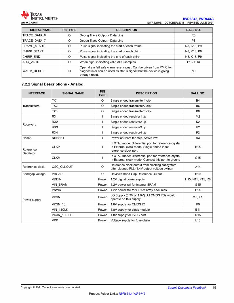
7.2.2 Signal Descriptions - Analog
INTERFACE SIGNAL NAME PIN TYPE DESCRIPTION BALL NO.
Transmitters
TX1 O Single ended transmitter1 o/p B4
TX2 O Single ended transmitter2 o/p B6
TX3 O Single ended transmitter3 o/p B8
Receivers
RX1 I Single ended receiver1 i/p M2
RX2 I Single ended receiver2 i/p K2
RX3 I Single ended receiver3 i/p H2
RX4 I Single ended receiver4 i/p F2
Reset NRESET I Power on reset for chip. Active low R3
Reference Oscillator
CLKP IIn XTAL mode: Differential port for reference crystalIn External clock mode: Single ended input reference clock port
B15
CLKM I In XTAL mode: Differential port for reference crystalIn External clock mode: Connect this port to ground C15
Reference clock OSC_CLKOUT O Reference clock output from clocking subsystem after cleanup PLL (1.4V output voltage swing). A14
Bandgap voltage VBGAP O Device's Band Gap Reference Output B10
Power supply
VDDIN Power 1.2V digital power supply H15, N11, P15, R6
VIN_SRAM Power 1.2V power rail for internal SRAM G15
VNWA Power 1.2V power rail for SRAM array back bias P14
VIOIN Power I/O Supply (3.3V or 1.8V): All CMOS I/Os would operate on this supply R10, F15
VIOIN_18 Power 1.8V supply for CMOS IO R9
VIN_18CLK Power 1.8V supply for clock module B11
VIOIN_18DIFF Power 1.8V supply for LVDS port D15
VPP Power Voltage supply for fuse chain L13
www.ti.comIWR6843, IWR6443
SWRS219E – OCTOBER 2018 – REVISED JUNE 2021
Copyright © 2021 Texas Instruments Incorporated Submit Document Feedback 15
Product Folder Links: IWR6843 IWR6443

INTERFACE SIGNAL NAME PIN TYPE DESCRIPTION BALL NO.
Power supply
VIN_13RF1 Power 1.3V Analog and RF supply,VIN_13RF1 and VIN_13RF2 could be shorted on the board G5, H5, J5
VIN_13RF2 Power 1.3V Analog and RF supply C2,D2
VIN_18BB Power 1.8V Analog base band power supply K5, F5
VIN_18VCO Power 1.8V RF VCO supply B12
VSS Ground Digital ground
L5, L6, L8, L10, K7, K8, K9, K10, K11,
J6, J7, J8, J10, H7, H9, H11, G6, G7, G8, G10, F9, F11, E5, E6, E8, E10,
E11, R15
VSSA Ground Analog ground
A1, A3, A5, A7, A9, A13, A15, B1, B3, B5, B7, B9, B14,
C1, C3, C4, C5, C6, C7, C8, C9, C14,
E1, E2, E3, F3, G1, G2, G3, H3, J1, J2, J3, K3, L1, L2, L3,
M3, N1, N2, N3, R1
Internal LDO output/inputs
VOUT_14APLL O Internal LDO output A10
VOUT_14SYNTH O Internal LDO output B13
VOUT_PA IO
Internal LDO output.When internal PA LDO is used, this pin provides the output voltage of the LDO. When the internal PA LDO is bypassed, and disabled, the 1-V supply should be fed on this pin. This is mandatory in the 3TX simultaneous use case.
A2, B2
Test and Debug output for pre-production phase. Can be pinned out on production hardware for field debug
Analog Test1 / GPADC1 IO Analog IO dedicated for ADC service P1
Analog Test2 / GPADC2 IO Analog IO dedicated for ADC service P2
Analog Test3 / GPADC3 IO Analog IO dedicated for ADC service P3
Analog Test4 / GPADC4 IO Analog IO dedicated for ADC service R2
ANAMUX / GPADC5 IO Analog IO dedicated for ADC service C13
VSENSE / GPADC6 IO Analog IO dedicated for ADC service D14
IWR6843, IWR6443SWRS219E – OCTOBER 2018 – REVISED JUNE 2021 www.ti.com
16 Submit Document Feedback Copyright © 2021 Texas Instruments Incorporated
Product Folder Links: IWR6843 IWR6443

7.3 Pin AttributesTable 7-1. Pin Attributes (ABL0161 Package)
BALL NUMBER [1] BALL NAME [2] SIGNAL NAME [3] PINCNTL ADDRESS[4] MODE [5] [9] TYPE [6] BALL RESET
STATE [7]PULL UP/DOWN
TYPE [8]
H13 GPIO_0 GPIO_13 0xFFFFEA04 0 IO Output Disabled Pull Down
GPIO_0 1 IO
PMIC_CLKOUT 2 O
EPWM1B 10 O
ePWM2A 11 O
J13 GPIO_1 GPIO_16 0xFFFFEA08 0 IO Output Disabled Pull Down
GPIO_1 1 IO
SYNC_OUT 2 O
DMM_MUX_IN 12 I
SPIB_CS_N_1 13 IO
SPIB_CS_N_2 14 IO
EPWM1SYNCI 15 I
K13 GPIO_2 GPIO_26 0xFFFFEA64 0 IO Output Disabled Pull Down
GPIO_2 1 IO
OSC_CLKOUT 2 O
MSS_UARTB_TX 7 O
BSS_UART_TX 8 O
SYNC_OUT 9 O
PMIC_CLKOUT 10 O
CHIRP_START 11 O
CHIRP_END 12 O
FRAME_START 13 O
R4 GPIO_31 TRACE_DATA_0 0xFFFFEA7C 0 O Output Disabled Pull Down
GPIO_31 1 IO
DMM0 2 I
MSS_UARTA_TX 4 IO
P5 GPIO_32 TRACE_DATA_1 0xFFFFEA80 0 O Output Disabled Pull Down
GPIO_32 1 IO
DMM1 2 I
R5 GPIO_33 TRACE_DATA_2 0xFFFFEA84 0 O Output Disabled Pull Down
GPIO_33 1 IO
DMM2 2 I
P6 GPIO_34 TRACE_DATA_3 0xFFFFEA88 0 O Output Disabled Pull Down
GPIO_34 1 IO
DMM3 2 I
EPWM3SYNCO 4 O
www.ti.comIWR6843, IWR6443
SWRS219E – OCTOBER 2018 – REVISED JUNE 2021
Copyright © 2021 Texas Instruments Incorporated Submit Document Feedback 17
Product Folder Links: IWR6843 IWR6443

Table 7-1. Pin Attributes (ABL0161 Package) (continued)BALL NUMBER [1] BALL NAME [2] SIGNAL NAME [3] PINCNTL
ADDRESS[4] MODE [5] [9] TYPE [6] BALL RESET STATE [7]
PULL UP/DOWN TYPE [8]
R7 GPIO_35 TRACE_DATA_4 0xFFFFEA8C 0 O Output Disabled Pull Down
GPIO_35 1 IO
DMM4 2 I
EPWM2SYNCO 4 O
P7 GPIO_36 TRACE_DATA_5 0xFFFFEA90 0 O Output Disabled Pull Down
GPIO_36 1 IO
DMM5 2 I
MSS_UARTB_TX 5 O
R8 GPIO_37 TRACE_DATA_6 0xFFFFEA94 0 O Output Disabled Pull Down
GPIO_37 1 IO
DMM6 2 I
BSS_UART_TX 5 O
P8 GPIO_38 TRACE_DATA_7 0xFFFFEA98 0 O Output Disabled Pull Down
GPIO_38 1 IO
DMM7 2 I
DSS_UART_TX 5 O
N15 GPIO_47 TRACE_CLK 0xFFFFEABC 0 O Output Disabled Pull Down
GPIO_47 1 IO
DMM_CLK 2 I
N14 DMM_SYNC TRACE_CTL 0xFFFFEAC0 0 O Output Disabled Pull Down
DMM_SYNC 2 I
N8 MCU_CLKOUT GPIO_25 0xFFFFEA60 0 IO Output Disabled Pull Down
MCU_CLKOUT 1 O
CHIRP_START 2 O
CHIRP_END 6 O
FRAME_START 7 O
EPWM1A 12 O
N7 NERROR_IN NERROR_IN 0xFFFFEA44 0 I Input
N6 NERROR_OUT NERROR_OUT 0xFFFFEA4C 0 O Hi-Z (Open Drain)
P9 PMIC_CLKOUT SOP[2] 0xFFFFEA68 During Power Up I Output Disabled Pull Down
GPIO_27 0 IO
PMIC_CLKOUT 1 O
CHIRP_START 6 O
CHIRP_END 7 O
FRAME_START 8 O
EPWM1B 11 O
EPWM2A 12 O
IWR6843, IWR6443SWRS219E – OCTOBER 2018 – REVISED JUNE 2021 www.ti.com
18 Submit Document Feedback Copyright © 2021 Texas Instruments Incorporated
Product Folder Links: IWR6843 IWR6443

Table 7-1. Pin Attributes (ABL0161 Package) (continued)BALL NUMBER [1] BALL NAME [2] SIGNAL NAME [3] PINCNTL
ADDRESS[4] MODE [5] [9] TYPE [6] BALL RESET STATE [7]
PULL UP/DOWN TYPE [8]
R13 QSPI[0] GPIO_8 0xFFFFEA2C 0 IO Output Disabled Pull Down
QSPI[0] 1 IO
SPIB_MISO 2 IO
N12 QSPI[1] GPIO_9 0xFFFFEA30 0 IO Output Disabled Pull Down
QSPI[1] 1 I
SPIB_MOSI 2 IO
SPIB_CS_N_2 8 IO
R14 QSPI[2] GPIO_10 0xFFFFEA34 0 IO Output Disabled Pull Down
QSPI[2] 1 I
CAN_FD_TX 8 O
P12 QSPI[3] GPIO_11 0xFFFFEA38 0 IO Output Disabled Pull Down
QSPI[3] 1 I
CAN_FD_RX 8 I
R12 QSPI_CLK GPIO_7 0xFFFFEA3C 0 IO Output Disabled Pull Down
QSPI_CLK 1 O
SPIB_CLK 2 IO
DSS_UART_TX 6 O
P11 QSPI_CS_N GPIO_6 0xFFFFEA40 0 IO Output Disabled Pull Up
QSPI_CS_N 1 O
SPIB_CS_N 2 IO
N4 RS232_RX GPIO_15 0xFFFFEA74 0 IO Input Enabled Pull Up
RS232_RX 1 I
MSS_UARTA_RX 2 I
BSS_UART_TX 6 IO
MSS_UARTB_RX 7 IO
CAN_FD_RX 8 I
I2C_SCL 9 IO
EPWM2A 10 O
EPWM2B 11 O
EPWM3A 12 O
www.ti.comIWR6843, IWR6443
SWRS219E – OCTOBER 2018 – REVISED JUNE 2021
Copyright © 2021 Texas Instruments Incorporated Submit Document Feedback 19
Product Folder Links: IWR6843 IWR6443

Table 7-1. Pin Attributes (ABL0161 Package) (continued)BALL NUMBER [1] BALL NAME [2] SIGNAL NAME [3] PINCNTL
ADDRESS[4] MODE [5] [9] TYPE [6] BALL RESET STATE [7]
PULL UP/DOWN TYPE [8]
N5 RS232_TX GPIO_14 0xFFFFEA78 0 IO Output Enabled
RS232_TX 1 O
MSS_UARTA_TX 5 IO
MSS_UARTB_TX 6 IO
BSS_UART_TX 7 IO
CAN_FD_TX 10 O
I2C_SDA 11 IO
EPWM1A 12 O
EPWM1B 13 O
NDMM_EN 14 I
EPWM2A 15 O
E13 SPIA_CLK GPIO_3 0xFFFFEA14 0 IO Output Disabled Pull Up
SPIA_CLK 1 IO
DSS_UART_TX 7 O
E15 SPIA_CS_N GPIO_30 0xFFFFEA18 0 IO Output Disabled Pull Up
SPIA_CS_N 1 IO
E14 SPIA_MISO GPIO_20 0xFFFFEA10 0 IO Output Disabled Pull Up
SPIA_MISO 1 IO
CAN_FD_TX 2 O
D13 SPIA_MOSI GPIO_19 0xFFFFEA0C 0 IO Output Disabled Pull Up
SPIA_MOSI 1 IO
CAN_FD_RX 2 I
DSS_UART_TX 8 O
F14 SPIB_CLK GPIO_5 0xFFFFEA24 0 IO Output Disabled Pull Up
SPIB_CLK 1 IO
MSS_UARTA_RX 2 I
MSS_UARTB_TX 6 O
BSS_UART_TX 7 O
CAN_FD_RX 8 I
H14 SPIB_CS_N GPIO_4 0xFFFFEA28 0 IO Output Disabled Pull Up
SPIB_CS_N 1 IO
MSS_UARTA_TX 2 O
MSS_UARTB_TX 6 O
BSS_UART_TX 7 IO
QSPI_CLK_EXT 8 I
CAN_FD_TX 9 O
IWR6843, IWR6443SWRS219E – OCTOBER 2018 – REVISED JUNE 2021 www.ti.com
20 Submit Document Feedback Copyright © 2021 Texas Instruments Incorporated
Product Folder Links: IWR6843 IWR6443

Table 7-1. Pin Attributes (ABL0161 Package) (continued)BALL NUMBER [1] BALL NAME [2] SIGNAL NAME [3] PINCNTL
ADDRESS[4] MODE [5] [9] TYPE [6] BALL RESET STATE [7]
PULL UP/DOWN TYPE [8]
G14 SPIB_MISO GPIO_22 0xFFFFEA20 0 IO Output Disabled Pull Up
SPIB_MISO 1 IO
I2C_SCL 2 IO
DSS_UART_TX 6 O
F13 SPIB_MOSI GPIO_21 0xFFFFEA1C 0 IO Output Disabled Pull Up
SPIB_MOSI 1 IO
I2C_SDA 2 IO
P13 SPI_HOST_INTR GPIO_12 0xFFFFEA00 0 IO Output Disabled Pull Down
SPI_HOST_INTR 1 O
SPIB_CS_N_1 6 IO
P4 SYNC_IN GPIO_28 0xFFFFEA6C 0 IO Output Disabled Pull Down
SYNC_IN 1 I
MSS_UARTB_RX 6 IO
DMM_MUX_IN 7 I
SYNC_OUT 9 O
G13 SYNC_OUT SOP[1] 0xFFFFEA70 During Power Up I Output Disabled Pull Down
GPIO_29 0 IO
SYNC_OUT 1 O
DMM_MUX_IN 9 I
SPIB_CS_N_1 10 IO
SPIB_CS_N_2 11 IO
P10 TCK GPIO_17 0xFFFFEA50 0 IO Input Enabled Pull Down
TCK 1 I
MSS_UARTB_TX 2 O
CAN_FD_TX 8 O
R11 TDI GPIO_23 0xFFFFEA58 0 IO Input Enabled Pull Up
TDI 1 I
MSS_UARTA_RX 2 I
N13 TDO SOP[0] 0xFFFFEA5C During Power Up I Output Enabled
GPIO_24 0 IO
TDO 1 O
MSS_UARTA_TX 2 O
MSS_UARTB_TX 6 O
BSS_UART_TX 7 O
NDMM_EN 9 I
N10 TMS GPIO_18 0xFFFFEA54 0 IO Input Enabled Pull Down
TMS 1 I
BSS_UART_TX 2 O
CAN_FD_RX 6 I
www.ti.comIWR6843, IWR6443
SWRS219E – OCTOBER 2018 – REVISED JUNE 2021
Copyright © 2021 Texas Instruments Incorporated Submit Document Feedback 21
Product Folder Links: IWR6843 IWR6443

Table 7-1. Pin Attributes (ABL0161 Package) (continued)BALL NUMBER [1] BALL NAME [2] SIGNAL NAME [3] PINCNTL
ADDRESS[4] MODE [5] [9] TYPE [6] BALL RESET STATE [7]
PULL UP/DOWN TYPE [8]
N9 WARM_RESET WARM_RESET 0xFFFFEA48 0 IO Hi-Z Input (Open Drain)
The following list describes the table column headers:
1. BALL NUMBER: Ball numbers on the bottom side associated with each signal on the bottom.2. BALL NAME: Mechanical name from package device (name is taken from muxmode 0).3. SIGNAL NAME: Names of signals multiplexed on each ball (also notice that the name of the ball is the signal name in muxmode 0).4. PINCNTL ADDRESS: MSS Address for PinMux Control5. MODE: Multiplexing mode number: value written to PinMux Cntl register to select specific Signal name for this Ball number. Mode column has bit
range value.6. TYPE: Signal type and direction:
• I = Input• O = Output• IO = Input or Output
7. BALL RESET STATE: The state of the terminal at power-on reset8. PULL UP/DOWN TYPE: indicates the presence of an internal pullup or pulldown resistor. Pullup and pulldown resistors can be enabled or disabled
via software.• Pull Up: Internal pullup• Pull Down: Internal pulldown• An empty box means No pull.
9. Pin Mux Control Value maps to lower 4 bits of register.
IWR6843, IWR6443SWRS219E – OCTOBER 2018 – REVISED JUNE 2021 www.ti.com
22 Submit Document Feedback Copyright © 2021 Texas Instruments Incorporated
Product Folder Links: IWR6843 IWR6443
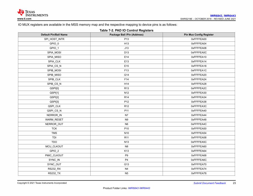
IO MUX registers are available in the MSS memory map and the respective mapping to device pins is as follows:
Table 7-2. PAD IO Control RegistersDefault Pin/Ball Name Package Ball /Pin (Address) Pin Mux Config Register
SPI_HOST_INTR P13 0xFFFFEA00
GPIO_0 H13 0xFFFFEA04
GPIO_1 J13 0xFFFFEA08
SPIA_MOSI D13 0xFFFFEA0C
SPIA_MISO E14 0xFFFFEA10
SPIA_CLK E13 0xFFFFEA14
SPIA_CS_N E15 0xFFFFEA18
SPIB_MOSI F13 0xFFFFEA1C
SPIB_MISO G14 0xFFFFEA20
SPIB_CLK F14 0xFFFFEA24
SPIB_CS_N H14 0xFFFFEA28
QSPI[0] R13 0xFFFFEA2C
QSPI[1] N12 0xFFFFEA30
QSPI[2] R14 0xFFFFEA34
QSPI[3] P12 0xFFFFEA38
QSPI_CLK R12 0xFFFFEA3C
QSPI_CS_N P11 0xFFFFEA40
NERROR_IN N7 0xFFFFEA44
WARM_RESET N9 0xFFFFEA48
NERROR_OUT N6 0xFFFFEA4C
TCK P10 0xFFFFEA50
TMS N10 0xFFFFEA54
TDI R11 0xFFFFEA58
TDO N13 0xFFFFEA5C
MCU_CLKOUT N8 0xFFFFEA60
GPIO_2 K13 0xFFFFEA64
PMIC_CLKOUT P9 0xFFFFEA68
SYNC_IN P4 0xFFFFEA6C
SYNC_OUT G13 0xFFFFEA70
RS232_RX N4 0xFFFFEA74
RS232_TX N5 0xFFFFEA78
www.ti.comIWR6843, IWR6443
SWRS219E – OCTOBER 2018 – REVISED JUNE 2021
Copyright © 2021 Texas Instruments Incorporated Submit Document Feedback 23
Product Folder Links: IWR6843 IWR6443

Table 7-2. PAD IO Control Registers (continued)Default Pin/Ball Name Package Ball /Pin (Address) Pin Mux Config Register
GPIO_31 R4 0xFFFFEA7C
GPIO_32 P5 0xFFFFEA80
GPIO_33 R5 0xFFFFEA84
GPIO_34 P6 0xFFFFEA88
GPIO_35 R7 0xFFFFEA8C
GPIO_36 P7 0xFFFFEA90
GPIO_37 R8 0xFFFFEA94
GPIO_38 P8 0xFFFFEA98
GPIO_47 N15 0xFFFFEABC
DMM_SYNC N14 0xFFFFEAC0
The register layout is as follows:
Table 7-3. PAD IO Register Bit DescriptionsBIT FIELD TYPE RESET (POWER
ON DEFAULT) DESCRIPTION
31-11 NU RW 0 Reserved
10 SC RW 0 IO slew rate control:0 = Higher slew rate1 = Lower slew rate
9 PUPDSEL RW 0 Pullup/PullDown Selection0 = Pull Down1 = Pull Up (This field is valid only if Pull Inhibit is set as '0')
8 PI RW 0 Pull Inhibit/Pull Disable0 = Enable1 = Disable
7 OE_OVERRIDE RW 1 Output Override
6 OE_OVERRIDE_CTRL RW 1 Output Override Control:(A '1' here overrides any o/p manipulation of this IO by any of the peripheral block hardware it is associated with for example a SPI Chip select)
5 IE_OVERRIDE RW 0 Input Override
4 IE_OVERRIDE_CTRL RW 0 Input Override Control:(A '1' here overrides any i/p value on this IO with a desired value)
3-0 FUNC_SEL RW 1 Function select for Pin Multiplexing (Refer to the Pin Mux Sheet)
IWR6843, IWR6443SWRS219E – OCTOBER 2018 – REVISED JUNE 2021 www.ti.com
24 Submit Document Feedback Copyright © 2021 Texas Instruments Incorporated
Product Folder Links: IWR6843 IWR6443
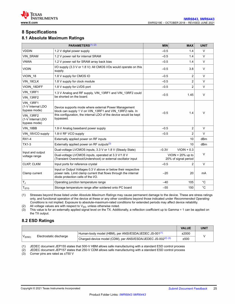
8 Specifications8.1 Absolute Maximum Ratings
PARAMETERS(1) (2) MIN MAX UNITVDDIN 1.2 V digital power supply –0.5 1.4 V
VIN_SRAM 1.2 V power rail for internal SRAM –0.5 1.4 V
VNWA 1.2 V power rail for SRAM array back bias –0.5 1.4 V
VIOIN I/O supply (3.3 V or 1.8 V): All CMOS I/Os would operate on this supply. –0.5 3.8 V
VIOIN_18 1.8 V supply for CMOS IO –0.5 2 V
VIN_18CLK 1.8 V supply for clock module –0.5 2 V
VIOIN_18DIFF 1.8 V supply for LVDS port –0.5 2 V
VIN_13RF1 1.3 V Analog and RF supply, VIN_13RF1 and VIN_13RF2 could be shorted on the board. –0.5 1.45 V
VIN_13RF2
VIN_13RF1(1-V Internal LDO bypass mode)
Device supports mode where external Power Management block can supply 1 V on VIN_13RF1 and VIN_13RF2 rails. In this configuration, the internal LDO of the device would be kept bypassed.
–0.5 1.4 VVIN_13RF2(1-V Internal LDO bypass mode)
VIN_18BB 1.8-V Analog baseband power supply –0.5 2 V
VIN_18VCO supply 1.8-V RF VCO supply –0.5 2 V
RX1-4 Externally applied power on RF inputs 10 dBm
TX1-3 Externally applied power on RF outputs(3) 10 dBm
Input and output voltage range
Dual-voltage LVCMOS inputs, 3.3 V or 1.8 V (Steady State) –0.3V VIOIN + 0.3VDual-voltage LVCMOS inputs, operated at 3.3 V/1.8 V
(Transient Overshoot/Undershoot) or external oscillator inputVIOIN + 20% up to
20% of signal period
CLKP, CLKM Input ports for reference crystal –0.5 2 V
Clamp currentInput or Output Voltages 0.3 V above or below their respective power rails. Limit clamp current that flows through the internal diode protection cells of the I/O.
–20 20 mA
TJ Operating junction temperature range –40 105 °C
TSTG Storage temperature range after soldered onto PC board –55 150 °C
(1) Stresses beyond those listed under Absolute Maximum Ratings may cause permanent damage to the device. These are stress ratings only, and functional operation of the device at these or any other conditions beyond those indicated under Recommended Operating Conditions is not implied. Exposure to absolute-maximum-rated conditions for extended periods may affect device reliability.
(2) All voltage values are with respect to VSS, unless otherwise noted.(3) This value is for an externally applied signal level on the TX. Additionally, a reflection coefficient up to Gamma = 1 can be applied on
the TX output.
8.2 ESD RatingsVALUE UNIT
V(ESD) Electrostatic dischargeHuman-body model (HBM), per ANSI/ESDA/JEDEC JS-001(1) ±2000
VCharged-device model (CDM), per ANSI/ESDA/JEDEC JS-002(2) (3) ±500
(1) JEDEC document JEP155 states that 500-V HBM allows safe manufacturing with a standard ESD control process(2) JEDEC document JEP157 states that 250-V CDM allows safe manufacturing with a standard ESD control process(3) Corner pins are rated as ±750 V
www.ti.comIWR6843, IWR6443
SWRS219E – OCTOBER 2018 – REVISED JUNE 2021
Copyright © 2021 Texas Instruments Incorporated Submit Document Feedback 25
Product Folder Links: IWR6843 IWR6443

8.3 Power-On Hours (POH)JUNCTION
TEMPERATURE (Tj)(1)
OPERATING CONDITION NOMINAL CVDD VOLTAGE (V) POWER-ON HOURS [POH] (HOURS)
105°C Tj 50% RF duty cycle 1.2 100,000
(1) This information is provided solely for your convenience and does not extend or modify the warranty provided under TI's standard terms and conditions for TI semiconductor products.
IWR6843, IWR6443SWRS219E – OCTOBER 2018 – REVISED JUNE 2021 www.ti.com
26 Submit Document Feedback Copyright © 2021 Texas Instruments Incorporated
Product Folder Links: IWR6843 IWR6443
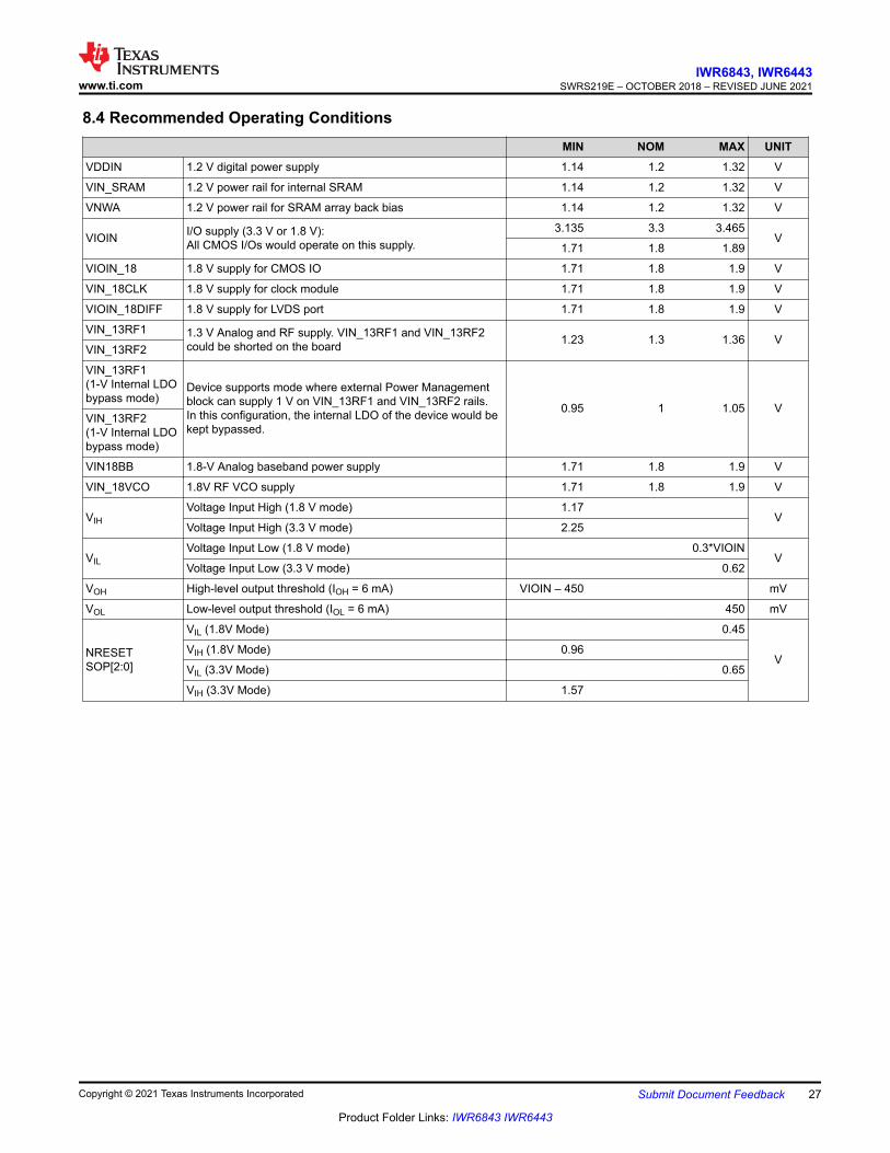
8.4 Recommended Operating ConditionsMIN NOM MAX UNIT
VDDIN 1.2 V digital power supply 1.14 1.2 1.32 V
VIN_SRAM 1.2 V power rail for internal SRAM 1.14 1.2 1.32 V
VNWA 1.2 V power rail for SRAM array back bias 1.14 1.2 1.32 V
VIOIN I/O supply (3.3 V or 1.8 V):All CMOS I/Os would operate on this supply.
3.135 3.3 3.465V
1.71 1.8 1.89
VIOIN_18 1.8 V supply for CMOS IO 1.71 1.8 1.9 V
VIN_18CLK 1.8 V supply for clock module 1.71 1.8 1.9 V
VIOIN_18DIFF 1.8 V supply for LVDS port 1.71 1.8 1.9 V
VIN_13RF1 1.3 V Analog and RF supply. VIN_13RF1 and VIN_13RF2 could be shorted on the board 1.23 1.3 1.36 V
VIN_13RF2
VIN_13RF1(1-V Internal LDO bypass mode)
Device supports mode where external Power Management block can supply 1 V on VIN_13RF1 and VIN_13RF2 rails. In this configuration, the internal LDO of the device would be kept bypassed.
0.95 1 1.05 VVIN_13RF2(1-V Internal LDO bypass mode)
VIN18BB 1.8-V Analog baseband power supply 1.71 1.8 1.9 V
VIN_18VCO 1.8V RF VCO supply 1.71 1.8 1.9 V
VIHVoltage Input High (1.8 V mode) 1.17
VVoltage Input High (3.3 V mode) 2.25
VILVoltage Input Low (1.8 V mode) 0.3*VIOIN
VVoltage Input Low (3.3 V mode) 0.62
VOH High-level output threshold (IOH = 6 mA) VIOIN – 450 mV
VOL Low-level output threshold (IOL = 6 mA) 450 mV
NRESET SOP[2:0]
VIL (1.8V Mode) 0.45
VVIH (1.8V Mode) 0.96
VIL (3.3V Mode) 0.65
VIH (3.3V Mode) 1.57
www.ti.comIWR6843, IWR6443
SWRS219E – OCTOBER 2018 – REVISED JUNE 2021
Copyright © 2021 Texas Instruments Incorporated Submit Document Feedback 27
Product Folder Links: IWR6843 IWR6443

8.5 Power Supply SpecificationsTable 8-1 describes the four rails from an external power supply block of the IWR6843 device.
Table 8-1. Power Supply Rails CharacteristicsSUPPLY DEVICE BLOCKS POWERED FROM THE SUPPLY RELEVANT IOS IN THE DEVICE
1.8 V Synthesizer and APLL VCOs, crystal oscillator, IF Amplifier stages, ADC, LVDS
Input: VIN_18VCO, VIN18CLK, VIN_18BB, VIOIN_18DIFF, VIOIN_18LDO Output: VOUT_14SYNTH, VOUT_14APLL
1.3 V (or 1 V in internal LDO bypass mode)(1)
Power Amplifier, Low Noise Amplifier, Mixers and LO Distribution
Input: VIN_13RF2, VIN_13RF1LDO Output: VOUT_PA
3.3 V (or 1.8 V for 1.8 V I/O mode) Digital I/Os Input VIOIN
1.2 V Core Digital and SRAMs Input: VDDIN, VIN_SRAM
(1) Three simultaneous transmitter operation is supported only in 1-V LDO bypass and PA LDO disable mode. In this mode 1V supply needs to be fed on the VOUT PA pin.
The 1.3-V (1.0 V) and 1.8-V power supply ripple specifications mentioned in Table 8-2 are defined to meet a target spur level of –105 dBc (RF Pin = –15 dBm) at the RX. The spur and ripple levels have a dB-to-dB relationship, for example, a 1-dB increase in supply ripple leads to a ~1 dB increase in spur level. Values quoted are rms levels for a sinusoidal input applied at the specified frequency.
Table 8-2. Ripple Specifications
FREQUENCY (kHz)RF RAIL VCO/IF RAIL
1.0 V (INTERNAL LDO BYPASS) (µVRMS) 1.3 V (µVRMS) 1.8 V (µVRMS)
137.5 7 648 83
275 5 76 21
550 3 22 11
1100 2 4 6
2200 11 82 13
4400 13 93 19
6600 22 117 29
IWR6843, IWR6443SWRS219E – OCTOBER 2018 – REVISED JUNE 2021 www.ti.com
28 Submit Document Feedback Copyright © 2021 Texas Instruments Incorporated
Product Folder Links: IWR6843 IWR6443

8.6 Power Consumption SummaryTable 8-3 and Table 8-4 summarize the power consumption at the power terminals.
Table 8-3. Maximum Current Ratings at Power TerminalsPARAMETER SUPPLY NAME DESCRIPTION MIN TYP MAX UNIT
Current consumption(1)
VDDIN, VIN_SRAM, VNWA Total current drawn by all nodes driven by 1.2V rail 1000
mA
VIN_13RF1, VIN_13RF2
Total current drawn by all nodes driven by 1.3V rail (or 1V rail in LDO Bypass mode), when only 2 transmitters are used.(3)
2000
VIOIN_18, VIN_18CLK, VIOIN_18DIFF, VIN_18BB, VIN_18VCO
Total current drawn by all nodes driven by 1.8V rail 850
VIOINTotal current drawn by all nodes driven by 3.3V rail(2)
50
(1) The specified current values are at typical supply voltage level.(2) The exact VIOIN current depends on the peripherals used and their frequency of operation.(3) Simultaneous 3 Transmitter operation is supported only with 1-V LDO bypass and PA LDO disable mode. In this mode, the 1-V supply
needs to be fed on the VOUT_PA pin. In this case, the peak 1-V supply current goes up to 2500 mA. To enable the LDO bypass mode, see the Interface Control document in the mmWave software development kit (SDK).
Table 8-4. Average Power Consumption at Power TerminalsPARAMETER CONDITION DESCRIPTION MIN TYP MAX UNIT
Average power consumption
1.0-V internal LDO bypass mode
24% duty cycle
1TX, 4RX Regular power ADC mode 6.4 Msps complex transceiver, 13.13-ms frame, 64 chirps, 256 samples/chirp, 8.5-µs interchirp time, DSP + Hardware accelerator active
1.19
W
2TX, 4RX(1) 1.25
48% duty cycle
1TX, 4RX Regular power ADC mode 6.4 Msps complex transceiver, 13.13-ms frame, 64 chirps, 256 samples/chirp, 8.5-µs interchirp time, DSP + Hardware accelerator active
1.62
2TX, 4RX(1) 1.75
(1) Two TX antennas are on simultaneously.
www.ti.comIWR6843, IWR6443
SWRS219E – OCTOBER 2018 – REVISED JUNE 2021
Copyright © 2021 Texas Instruments Incorporated Submit Document Feedback 29
Product Folder Links: IWR6843 IWR6443
8.7 RF Specificationover recommended operating conditions (unless otherwise noted)
PARAMETER MIN TYP MAX UNIT
Receiver
Noise figure 60 to 64 GHz 12 dB
1-dB compression point (Out Of Band)(1) –12 dBm
Maximum gain 48 dB
Gain range 18 dB
Gain step size 2 dB
IF bandwidth(2) 10 MHz
ADC sampling rate (real) 25 Msps
ADC sampling rate (complex 1x) 12.5 Msps
ADC resolution 12 Bits
Idle Channel Spurs –90 dBFS
TransmitterOutput power 12 dBm
Power backoff range 26 dB
Clock subsystem
Frequency range 60 64 GHz
Ramp rate 250 MHz/µs
Phase noise at 1-MHz offset 60 to 64 GHz –93 dBc/Hz
(1) 1-dB Compression Point (Out Of Band) is measured by feed a Continuous wave Tone (10 kHz) well below the lowest HPF cut-off frequency.
(2) The analog IF stages include high-pass filtering, with two independently configurable first-order high-pass corner frequencies. The set of available HPF corners is summarized as follows:Available HPF Corner Frequencies (kHz)HPF1 HPF2175, 235, 350, 700 350, 700, 1400, 2800
The filtering performed by the digital baseband chain is targeted to provide:• Less than ±0.5 dB pass-band ripple/droop, and• Better than 60 dB anti-aliasing attenuation for any frequency that can alias back into the pass-band.
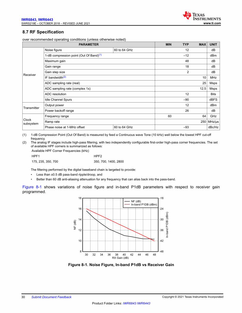
Figure 8-1 shows variations of noise figure and in-band P1dB parameters with respect to receiver gain programmed.
RX Gain (dB)
NF
(dB
)
In-b
an
dP
1D
B(d
Bm
)
8 -48
10 -42
12 -36
14 -30
16 -24
18 -18
30 32 34 36 38 40 42 44 46 48
NF (dB)In-band P1DB (dBm)
Figure 8-1. Noise Figure, In-band P1dB vs Receiver Gain
IWR6843, IWR6443SWRS219E – OCTOBER 2018 – REVISED JUNE 2021 www.ti.com
30 Submit Document Feedback Copyright © 2021 Texas Instruments Incorporated
Product Folder Links: IWR6843 IWR6443

8.8 CPU Specificationsover recommended operating conditions (unless otherwise noted)
PARAMETER MIN TYP MAX UNIT
DSP Subsystem (C674 Family)
Clock Speed 600 MHz
L1 Code Memory 32 KB
L1 Data Memory 32 KB
L2 Memory 256 KB
Main Subsystem (R4F Family)
Clock Speed 200 MHz
Tightly Coupled Memory - A (Program) 512 KB
Tightly Coupled Memory - B (Data) 192 KB
Shared Memory Shared L3 Memory 768 KB
www.ti.comIWR6843, IWR6443
SWRS219E – OCTOBER 2018 – REVISED JUNE 2021
Copyright © 2021 Texas Instruments Incorporated Submit Document Feedback 31
Product Folder Links: IWR6843 IWR6443

8.9 Thermal Resistance Characteristics for FCBGA Package [ABL0161] THERMAL METRICS(1) °C/W(2) (3)
RΘJC Junction-to-case 4.92
RΘJB Junction-to-board 6.57
RΘJA Junction-to-free air 22.3
RΘJMA Junction-to-moving air N/A (4)
PsiJT Junction-to-package top 4.92
PsiJB Junction-to-board 6.4
(1) For more information about traditional and new thermal metrics, see Semiconductor and IC Package Thermal Metrics.(2) °C/W = degrees Celsius per watt.(3) These values are based on a JEDEC-defined 2S2P system (with the exception of the Theta JC [RΘJC] value, which is based on
a JEDEC-defined 1S0P system) and will change based on environment as well as application. For more information, see these EIA/JEDEC standards:• JESD51-2, Integrated Circuits Thermal Test Method Environmental Conditions - Natural Convection (Still Air)• JESD51-3, Low Effective Thermal Conductivity Test Board for Leaded Surface Mount Packages• JESD51-7, High Effective Thermal Conductivity Test Board for Leaded Surface Mount Packages• JESD51-9, Test Boards for Area Array Surface Mount Package Thermal Measurements
(4) N/A = not applicable
8.10 Timing and Switching Characteristics8.10.1 Power Supply Sequencing and Reset Timing
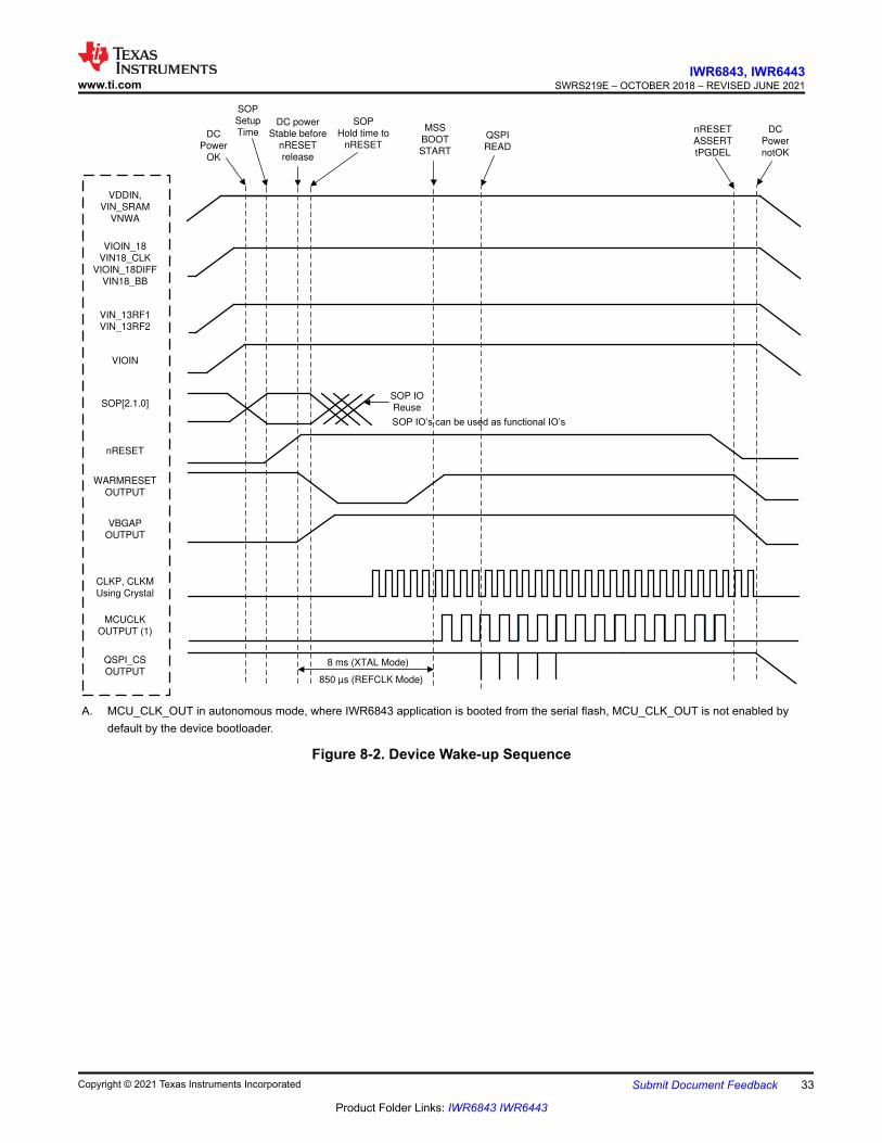
The IWR6843 device expects all external voltage rails to be stable before reset is deasserted. Figure 8-2 describes the device wake-up sequence.
IWR6843, IWR6443SWRS219E – OCTOBER 2018 – REVISED JUNE 2021 www.ti.com
32 Submit Document Feedback Copyright © 2021 Texas Instruments Incorporated
Product Folder Links: IWR6843 IWR6443
VDDIN, VIN_SRAM
VNWA
WARMRESETOUTPUT
VIOIN_18VIN18_CLK
VIOIN_18DIFFVIN18_BB
VIN_13RF1VIN_13RF2
VIOIN
nRESET
SOP[2.1.0]
VBGAPOUTPUT
CLKP, CLKMUsing Crystal
MCUCLKOUTPUT (1)
QSPI_CSOUTPUT
DC powerStable before
nRESET release
SOPSetupTime
SOPHold time to
nRESETDC
PowerOK
MSSBOOTSTART
QSPIREAD
nRESETASSERTtPGDEL
DCPowernotOK
8 ms (XTAL Mode)
850 µs (REFCLK Mode)
SOP IOReuse
623�,2¶V�FDQ�EH�XVHG�DV�IXQFWLRQDO�,2¶V
A. MCU_CLK_OUT in autonomous mode, where IWR6843 application is booted from the serial flash, MCU_CLK_OUT is not enabled by default by the device bootloader.
Figure 8-2. Device Wake-up Sequence
www.ti.comIWR6843, IWR6443
SWRS219E – OCTOBER 2018 – REVISED JUNE 2021
Copyright © 2021 Texas Instruments Incorporated Submit Document Feedback 33
Product Folder Links: IWR6843 IWR6443
8.10.2 Input Clocks and Oscillators8.10.2.1 Clock Specifications
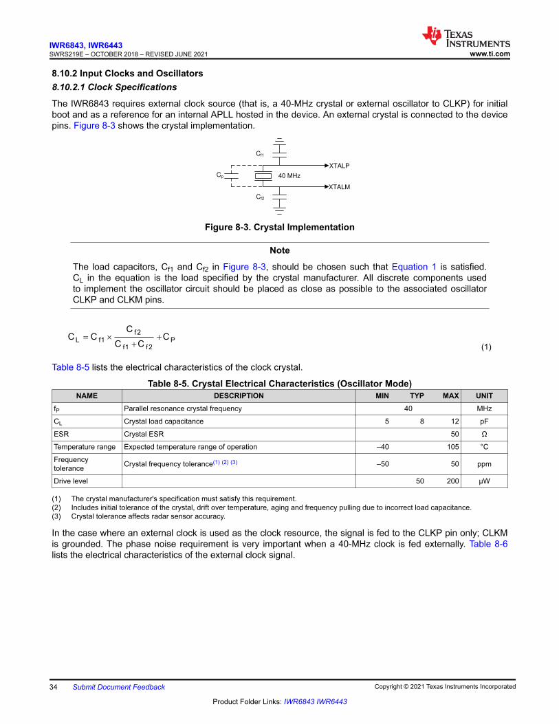
The IWR6843 requires external clock source (that is, a 40-MHz crystal or external oscillator to CLKP) for initial boot and as a reference for an internal APLL hosted in the device. An external crystal is connected to the device pins. Figure 8-3 shows the crystal implementation.
40 MHz
XTALP
XTALM
Cf1
Cf2
Cp
Figure 8-3. Crystal Implementation
Note
The load capacitors, Cf1 and Cf2 in Figure 8-3, should be chosen such that Equation 1 is satisfied. CL in the equation is the load specified by the crystal manufacturer. All discrete components used to implement the oscillator circuit should be placed as close as possible to the associated oscillator CLKP and CLKM pins.
f2
L f1 P
f1 f2
CC C C
C C= ´ +
+ (1)
Table 8-5 lists the electrical characteristics of the clock crystal.
Table 8-5. Crystal Electrical Characteristics (Oscillator Mode)NAME DESCRIPTION MIN TYP MAX UNIT
fP Parallel resonance crystal frequency 40 MHz
CL Crystal load capacitance 5 8 12 pF
ESR Crystal ESR 50 Ω
Temperature range Expected temperature range of operation –40 105 °C
Frequency tolerance Crystal frequency tolerance(1) (2) (3) –50 50 ppm
Drive level 50 200 µW
(1) The crystal manufacturer's specification must satisfy this requirement.(2) Includes initial tolerance of the crystal, drift over temperature, aging and frequency pulling due to incorrect load capacitance.(3) Crystal tolerance affects radar sensor accuracy.
In the case where an external clock is used as the clock resource, the signal is fed to the CLKP pin only; CLKM is grounded. The phase noise requirement is very important when a 40-MHz clock is fed externally. Table 8-6 lists the electrical characteristics of the external clock signal.
IWR6843, IWR6443SWRS219E – OCTOBER 2018 – REVISED JUNE 2021 www.ti.com
34 Submit Document Feedback Copyright © 2021 Texas Instruments Incorporated
Product Folder Links: IWR6843 IWR6443
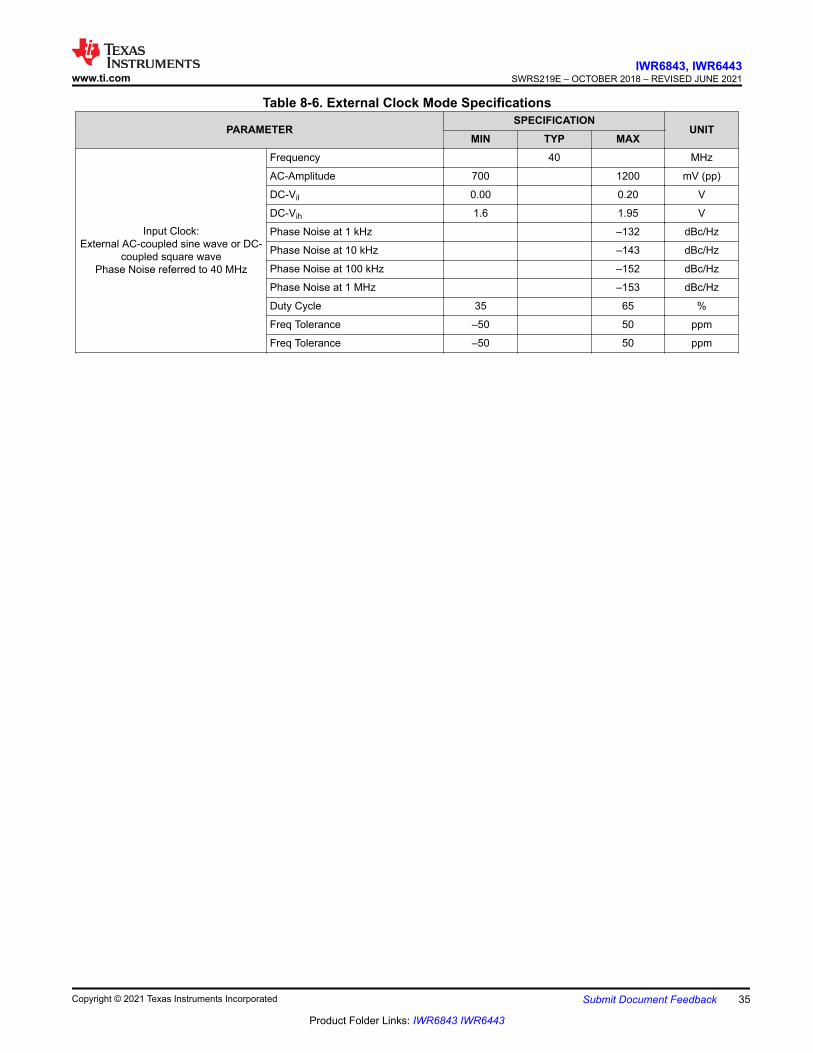
Table 8-6. External Clock Mode Specifications
PARAMETERSPECIFICATION
UNITMIN TYP MAX
Input Clock:External AC-coupled sine wave or DC-
coupled square wavePhase Noise referred to 40 MHz
Frequency 40 MHz
AC-Amplitude 700 1200 mV (pp)
DC-Vil 0.00 0.20 V
DC-Vih 1.6 1.95 V
Phase Noise at 1 kHz –132 dBc/Hz
Phase Noise at 10 kHz –143 dBc/Hz
Phase Noise at 100 kHz –152 dBc/Hz
Phase Noise at 1 MHz –153 dBc/Hz
Duty Cycle 35 65 %
Freq Tolerance –50 50 ppm
Freq Tolerance –50 50 ppm
www.ti.comIWR6843, IWR6443
SWRS219E – OCTOBER 2018 – REVISED JUNE 2021
Copyright © 2021 Texas Instruments Incorporated Submit Document Feedback 35
Product Folder Links: IWR6843 IWR6443

8.10.3 Multibuffered / Standard Serial Peripheral Interface (MibSPI)8.10.3.1 Peripheral Description
The SPI uses a MibSPI Protocol by TI.
The MibSPI/SPI is a high-speed synchronous serial input/output port that allows a serial bit stream of programmed length (2 to 16 bits) to be shifted into and out of the device at a programmed bit-transfer rate. The MibSPI/SPI is normally used for communication between the microcontroller and external peripherals or another microcontroller.
Standard and MibSPI modules have the following features:• 16-bit shift register• Receive buffer register• 8-bit baud clock generator• SPICLK can be internally-generated (master mode) or received from an external clock source
(slave mode)• Each word transferred can have a unique format.• SPI I/Os not used in the communication can be used as digital input/output signals
8.10.3.2 MibSPI Transmit and Receive RAM Organization
The Multibuffer RAM is comprised of 256 buffers. Each entry in the Multibuffer RAM consists of 4 parts: a 16-bit transmit field, a 16-bit receive field, a 16-bit control field and a 16-bit status field. The Multibuffer RAM can be partitioned into multiple transfer group with variable number of buffers each.
Section 8.10.3.2.2 and Section 8.10.3.2.3 assume the operating conditions stated in Section 8.10.3.2.1.
8.10.3.2.1 SPI Timing Conditions
MIN TYP MAX UNITInput Conditions
tR Input rise time 1 3 ns
tF Input fall time 1 3 ns
Output Conditions
CLOAD Output load capacitance 2 15 pF
8.10.3.2.2 SPI Master Mode Switching Parameters (CLOCK PHASE = 0, SPICLK = output,SPISIMO = output, and SPISOMI = input)(1) (2) (3)
NO. PARAMETER MIN TYP MAX UNIT1 tc(SPC)M Cycle time, SPICLK(4) 25 256tc(VCLK) ns
2(4)tw(SPCH)M Pulse duration, SPICLK high (clock polarity = 0) 0.5tc(SPC)M – 4 0.5tc(SPC)M + 4
nstw(SPCL)M Pulse duration, SPICLK low (clock polarity = 1) 0.5tc(SPC)M – 4 0.5tc(SPC)M + 4
3(4)tw(SPCL)M Pulse duration, SPICLK low (clock polarity = 0) 0.5tc(SPC)M – 4 0.5tc(SPC)M + 4
nstw(SPCH)M Pulse duration, SPICLK high (clock polarity = 1) 0.5tc(SPC)M – 4 0.5tc(SPC)M + 4
4(4)
td(SPCH-SIMO)M
Delay time, SPISIMO valid before SPICLK low, (clock polarity = 0)
0.5tc(SPC)M – 3
nstd(SPCL-SIMO)M
Delay time, SPISIMO valid before SPICLK high, (clock polarity = 1)
0.5tc(SPC)M – 3
5(4)
tv(SPCL-SIMO)M
Valid time, SPISIMO data valid after SPICLK low, (clock polarity = 0)
0.5tc(SPC)M – 10.5
nstv(SPCH-SIMO)M
Valid time, SPISIMO data valid after SPICLK high, (clock polarity = 1)
0.5tc(SPC)M – 10.5
IWR6843, IWR6443SWRS219E – OCTOBER 2018 – REVISED JUNE 2021 www.ti.com
36 Submit Document Feedback Copyright © 2021 Texas Instruments Incorporated
Product Folder Links: IWR6843 IWR6443

NO. PARAMETER MIN TYP MAX UNIT
6(5) tC2TDELAY
Setup time CS active until SPICLK high(clock polarity = 0)
CSHOLD = 0 (C2TDELAY+2)*tc(VCLK) – 7.5
(C2TDELAY+2) * tc(VCLK) + 7
ns
CSHOLD = 1 (C2TDELAY +3) * tc(VCLK) – 7.5
(C2TDELAY+3) * tc(VCLK) + 7
Setup time CS active until SPICLK low(clock polarity = 1)
CSHOLD = 0 (C2TDELAY+2)*tc(VCLK) – 7.5
(C2TDELAY+2) * tc(VCLK) + 7
CSHOLD = 1 (C2TDELAY +3) * tc(VCLK) – 7.5
(C2TDELAY+3) * tc(VCLK) + 7
7(5) tT2CDELAY
Hold time, SPICLK low until CS inactive (clock polarity = 0) 0.5*tc(SPC)M + (T2CDELAY + 1) *tc(VCLK) – 7
0.5*tc(SPC)M + (T2CDELAY + 1) * tc(VCLK) +
7.5ns
Hold time, SPICLK high until CS inactive (clock polarity = 1) 0.5*tc(SPC)M + (T2CDELAY + 1) *tc(VCLK) – 7
0.5*tc(SPC)M + (T2CDELAY + 1) * tc(VCLK) +
7.5
8(4)
tsu(SOMI-SPCL)M
Setup time, SPISOMI before SPICLK low(clock polarity = 0) 5
nstsu(SOMI-SPCH)M
Setup time, SPISOMI before SPICLK high(clock polarity = 1) 5
9(4)
th(SPCL-SOMI)M
Hold time, SPISOMI data valid after SPICLK low(clock polarity = 0) 3
nsth(SPCH-SOMI)M
Hold time, SPISOMI data valid after SPICLK high(clock polarity = 1) 3
(1) The MASTER bit (SPIGCRx.0) is set and the CLOCK PHASE bit (SPIFMTx.16) is cleared (where x= 0 or 1).(2) tc(MSS_VCLK) = master subsystem clock time = 1 / f(MSS_VCLK). For more details, see the Technical Reference Manual.(3) When the SPI is in Master mode, the following must be true: For PS values from 1 to 255: tc(SPC)M ≥ (PS +1)tc(MSS_VCLK) ≥ 25ns, where
PS is the prescale value set in the SPIFMTx.[15:8] register bits. For PS values of 0: tc(SPC)M = 2tc(MSS_VCLK) ≥ 25ns.(4) The active edge of the SPICLK signal referenced is controlled by the CLOCK POLARITY bit (SPIFMTx.17).(5) C2TDELAY and T2CDELAY is programmed in the SPIDELAY register
SPICLK(clock polarity = 0)
SPICLK(clock polarity = 1
SPISIMO
SPISOMI
Master Out Data Is Valid
Master In DataMust Be Valid
1
4 5
9
1
12
1
3
1
1
2
8
Figure 8-4. SPI Master Mode External Timing (CLOCK PHASE = 0)
www.ti.comIWR6843, IWR6443
SWRS219E – OCTOBER 2018 – REVISED JUNE 2021
Copyright © 2021 Texas Instruments Incorporated Submit Document Feedback 37
Product Folder Links: IWR6843 IWR6443
SPICLK
(clock polarity=0)
SPISIMO
SPICSn
Master Out Data Is Valid
7
SPICLK
(clock polarity=1)
Write to buffer
6
Figure 8-5. SPI Master Mode Chip Select Timing (CLOCK PHASE = 0)
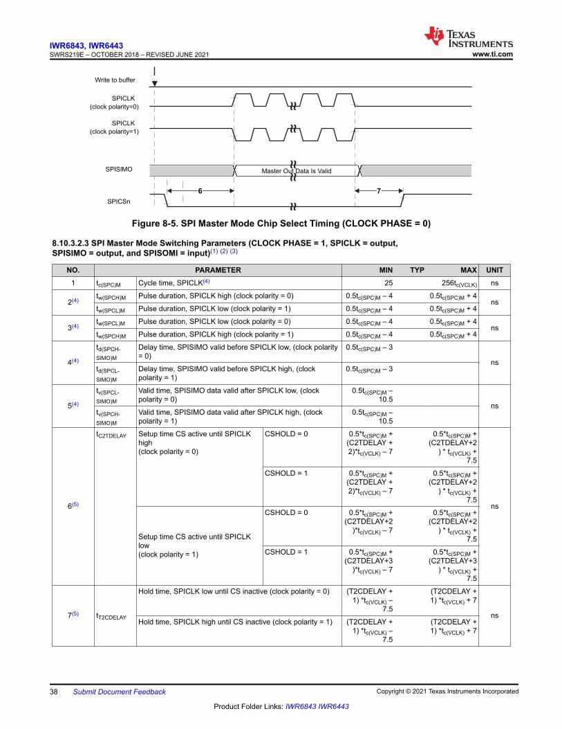
8.10.3.2.3 SPI Master Mode Switching Parameters (CLOCK PHASE = 1, SPICLK = output,SPISIMO = output, and SPISOMI = input)(1) (2) (3)
NO. PARAMETER MIN TYP MAX UNIT1 tc(SPC)M Cycle time, SPICLK(4) 25 256tc(VCLK) ns
2(4)tw(SPCH)M Pulse duration, SPICLK high (clock polarity = 0) 0.5tc(SPC)M – 4 0.5tc(SPC)M + 4
nstw(SPCL)M Pulse duration, SPICLK low (clock polarity = 1) 0.5tc(SPC)M – 4 0.5tc(SPC)M + 4
3(4)tw(SPCL)M Pulse duration, SPICLK low (clock polarity = 0) 0.5tc(SPC)M – 4 0.5tc(SPC)M + 4
nstw(SPCH)M Pulse duration, SPICLK high (clock polarity = 1) 0.5tc(SPC)M – 4 0.5tc(SPC)M + 4
4(4)
td(SPCH-SIMO)M
Delay time, SPISIMO valid before SPICLK low, (clock polarity = 0)
0.5tc(SPC)M – 3
nstd(SPCL-SIMO)M
Delay time, SPISIMO valid before SPICLK high, (clock polarity = 1)
0.5tc(SPC)M – 3
5(4)
tv(SPCL-SIMO)M
Valid time, SPISIMO data valid after SPICLK low, (clock polarity = 0)
0.5tc(SPC)M – 10.5
nstv(SPCH-SIMO)M
Valid time, SPISIMO data valid after SPICLK high, (clock polarity = 1)
0.5tc(SPC)M – 10.5
6(5)
tC2TDELAY Setup time CS active until SPICLK high(clock polarity = 0)
CSHOLD = 0 0.5*tc(SPC)M + (C2TDELAY + 2)*tc(VCLK) – 7
0.5*tc(SPC)M + (C2TDELAY+2
) * tc(VCLK) + 7.5
ns
CSHOLD = 1 0.5*tc(SPC)M + (C2TDELAY + 2)*tc(VCLK) – 7
0.5*tc(SPC)M + (C2TDELAY+2
) * tc(VCLK) + 7.5
Setup time CS active until SPICLK low(clock polarity = 1)
CSHOLD = 0 0.5*tc(SPC)M + (C2TDELAY+2
)*tc(VCLK) – 7
0.5*tc(SPC)M + (C2TDELAY+2
) * tc(VCLK) + 7.5
CSHOLD = 1 0.5*tc(SPC)M + (C2TDELAY+3
)*tc(VCLK) – 7
0.5*tc(SPC)M + (C2TDELAY+3
) * tc(VCLK) + 7.5
7(5) tT2CDELAY
Hold time, SPICLK low until CS inactive (clock polarity = 0) (T2CDELAY + 1) *tc(VCLK) –
7.5
(T2CDELAY + 1) *tc(VCLK) + 7
nsHold time, SPICLK high until CS inactive (clock polarity = 1) (T2CDELAY +
1) *tc(VCLK) – 7.5
(T2CDELAY + 1) *tc(VCLK) + 7
IWR6843, IWR6443SWRS219E – OCTOBER 2018 – REVISED JUNE 2021 www.ti.com
38 Submit Document Feedback Copyright © 2021 Texas Instruments Incorporated
Product Folder Links: IWR6843 IWR6443

NO. PARAMETER MIN TYP MAX UNIT
8(4)
tsu(SOMI-SPCL)M
Setup time, SPISOMI before SPICLK low(clock polarity = 0) 5
nstsu(SOMI-SPCH)M
Setup time, SPISOMI before SPICLK high(clock polarity = 1) 5
9(4)
th(SPCL-SOMI)M
Hold time, SPISOMI data valid after SPICLK low(clock polarity = 0) 3
nsth(SPCH-SOMI)M
Hold time, SPISOMI data valid after SPICLK high(clock polarity = 1) 3
(1) The MASTER bit (SPIGCRx.0) is set and the CLOCK PHASE bit (SPIFMTx.16) is set ( where x = 0 or 1 ).(2) tc(MSS_VCLK) = master subsystem clock time = 1 / f(MSS_VCLK). For more details, see the Technical Reference Manual.(3) When the SPI is in Master mode, the following must be true: For PS values from 1 to 255: tc(SPC)M ≥ (PS +1)tc(MSS_VCLK) ≥ 25 ns,
where PS is the prescale value set in the SPIFMTx.[15:8] register bits. For PS values of 0: tc(SPC)M = 2tc(MSS_VCLK) ≥ 25 ns.(4) The active edge of the SPICLK signal referenced is controlled by the CLOCK POLARITY bit (SPIFMTx.17).(5) C2TDELAY and T2CDELAY is programmed in the SPIDELAY register
www.ti.comIWR6843, IWR6443
SWRS219E – OCTOBER 2018 – REVISED JUNE 2021
Copyright © 2021 Texas Instruments Incorporated Submit Document Feedback 39
Product Folder Links: IWR6843 IWR6443
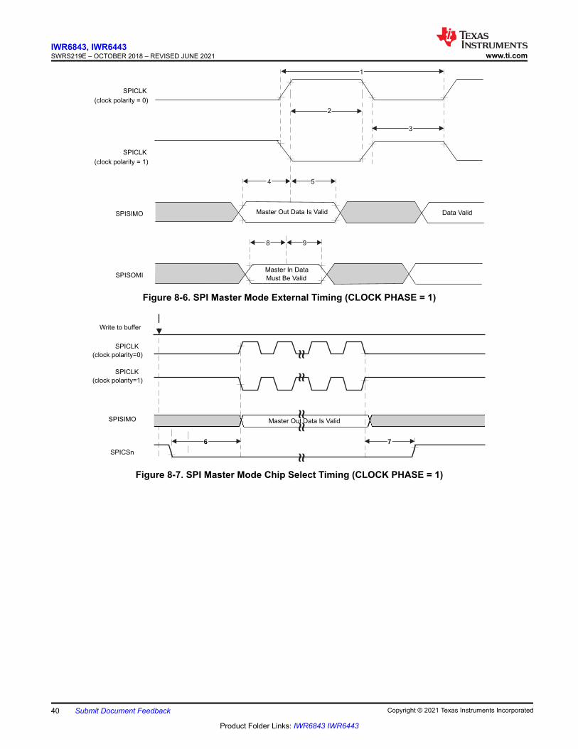
SPISOMI
SPISIMO
SPICLK
(clock polarity = 1)
SPICLK
(clock polarity = 0)
Data Valid
Master In Data
Must Be Valid
Master Out Data Is Valid
3
2
1
54
98
Figure 8-6. SPI Master Mode External Timing (CLOCK PHASE = 1)
SPICLK
(clock polarity=0)
SPISIMO
SPICSn
Master Out Data Is Valid
7
SPICLK
(clock polarity=1)
Write to buffer
6
Figure 8-7. SPI Master Mode Chip Select Timing (CLOCK PHASE = 1)
IWR6843, IWR6443SWRS219E – OCTOBER 2018 – REVISED JUNE 2021 www.ti.com
40 Submit Document Feedback Copyright © 2021 Texas Instruments Incorporated
Product Folder Links: IWR6843 IWR6443

8.10.3.3 SPI Slave Mode I/O Timings8.10.3.3.1 SPI Slave Mode Switching Parameters (SPICLK = input, SPISIMO = input,and SPISOMI = output)(1) (2) (3)
NO. PARAMETER MIN TYP MAX UNIT1 tc(SPC)S Cycle time, SPICLK(4) 25 ns
2(5)tw(SPCH)S Pulse duration, SPICLK high (clock polarity = 0) 10
nstw(SPCL)S Pulse duration, SPICLK low (clock polarity = 1) 10
3(5)tw(SPCL)S Pulse duration, SPICLK low (clock polarity = 0) 10
nstw(SPCH)S Pulse duration, SPICLK high (clock polarity = 1) 10
4(5)
td(SPCH-SOMI)S Delay time, SPISOMI valid after SPICLK high (clock polarity = 0) 10
nstd(SPCL-SOMI)S Delay time, SPISOMI valid after SPICLK low (clock
polarity = 1) 10
5(5)
th(SPCH-SOMI)S Hold time, SPISOMI data valid after SPICLK high (clock polarity = 0) 2
nsth(SPCL-SOMI)S Hold time, SPISOMI data valid after SPICLK low
(clock polarity = 1) 2
4(5)
td(SPCH-SOMI)S Delay time, SPISOMI valid after SPICLK high (clock polarity = 0; clock phase = 0) OR (clock polarity = 1; clock phase = 1)
10
nstd(SPCL-SOMI)S Delay time, SPISOMI valid after SPICLK low (clock
polarity = 1; clock phase = 0) OR (clock polarity = 0; clock phase = 1)
10
5(5)
th(SPCH-SOMI)S Hold time, SPISOMI data valid after SPICLK high (clock polarity = 0; clock phase = 0) OR (clock polarity = 1; clock phase = 1)
2
nsth(SPCL-SOMI)S Hold time, SPISOMI data valid after SPICLK low
(clock polarity = 1; clock phase = 0) OR (clock polarity = 0; clock phase = 1)
2
6(5)
tsu(SIMO-SPCL)S
Setup time, SPISIMO before SPICLK low (clock polarity = 0; clock phase = 0) OR (clock polarity = 1; clock phase = 1)
3
ns
tsu(SIMO-SPCH)S
Setup time, SPISIMO before SPICLK high (clock polarity = 1; clock phase = 0) OR (clock polarity = 0; clock phase = 1)
3
7(5)
th(SPCL-SIMO)S
Hold time, SPISIMO data valid after SPICLK low (clock polarity = 0; clock phase = 0) OR (clock polarity = 1; clock phase = 1)
1
ns
th(SPCL-SIMO)S
Hold time, SPISIMO data valid after SPICLK high (clock polarity = 1; clock phase = 0) OR (clock polarity = 0; clock phase = 1)
1
(1) The MASTER bit (SPIGCRx.0) is cleared ( where x = 0 or 1 ).(2) The CLOCK PHASE bit (SPIFMTx.16) is either cleared or set for CLOCK PHASE = 0 or CLOCK PHASE = 1 respectively.(3) tc(MSS_VCLK) = main subsystem clock time = 1 / f(MSS_VCLK). For more details, see the Technical Reference Manual.(4) When the SPI is in Slave mode, the following must be true: For PS values from 1 to 255: tc(SPC)S ≥ (PS +1)tc(MSS_VCLK) ≥ 25 ns, where
PS is the prescale value set in the SPIFMTx.[15:8] register bits.For PS values of 0: tc(SPC)S = 2tc(MSS_VCLK) ≥ 25 ns.(5) The active edge of the SPICLK signal referenced is controlled by the CLOCK POLARITY bit (SPIFMTx.17).
www.ti.comIWR6843, IWR6443
SWRS219E – OCTOBER 2018 – REVISED JUNE 2021
Copyright © 2021 Texas Instruments Incorporated Submit Document Feedback 41
Product Folder Links: IWR6843 IWR6443
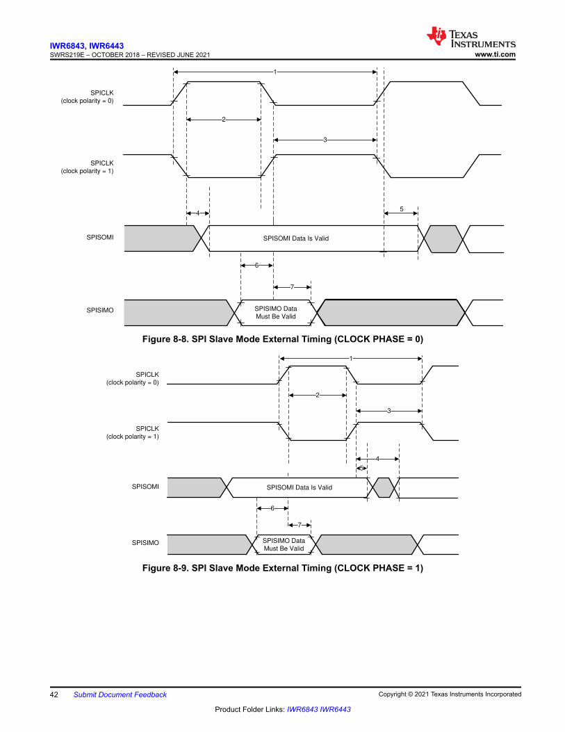
SPISIMO Data
Must Be Valid
SPISOMI Data Is Valid
6
7
2
1
3
SPICLK
(clock polarity = 0)
SPICLK
(clock polarity = 1)
SPISOMI
SPISIMO
45
Figure 8-8. SPI Slave Mode External Timing (CLOCK PHASE = 0)
SPISIMO Data
Must Be Valid
SPISOMI Data Is Valid
6
7
2
1
4
3
SPICLK
(clock polarity = 0)
SPICLK
(clock polarity = 1)
SPISOMI
SPISIMO
5
Figure 8-9. SPI Slave Mode External Timing (CLOCK PHASE = 1)
IWR6843, IWR6443SWRS219E – OCTOBER 2018 – REVISED JUNE 2021 www.ti.com
42 Submit Document Feedback Copyright © 2021 Texas Instruments Incorporated
Product Folder Links: IWR6843 IWR6443
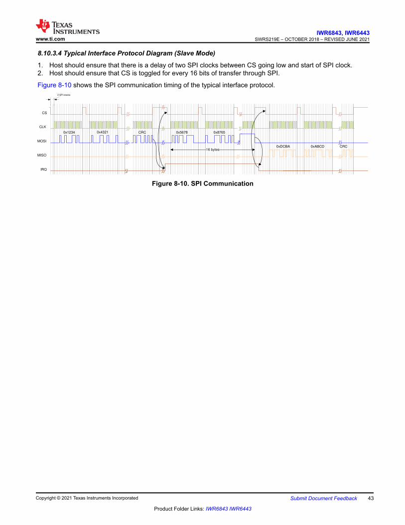
8.10.3.4 Typical Interface Protocol Diagram (Slave Mode)
1. Host should ensure that there is a delay of two SPI clocks between CS going low and start of SPI clock.2. Host should ensure that CS is toggled for every 16 bits of transfer through SPI.
Figure 8-10 shows the SPI communication timing of the typical interface protocol.
CS
CLK
MOSI
MISO
IRQ
0x56780x1234 0x4321 CRC
0xDCBA 0xABCD CRC
0x8765
16 bytes
2 SPI clocks
Figure 8-10. SPI Communication
www.ti.comIWR6843, IWR6443
SWRS219E – OCTOBER 2018 – REVISED JUNE 2021
Copyright © 2021 Texas Instruments Incorporated Submit Document Feedback 43
Product Folder Links: IWR6843 IWR6443
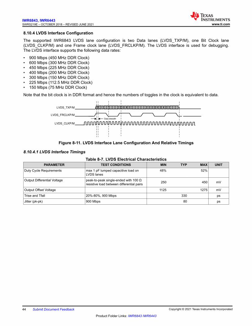
8.10.4 LVDS Interface Configuration
The supported IWR6843 LVDS lane configuration is two Data lanes (LVDS_TXP/M), one Bit Clock lane (LVDS_CLKP/M) and one Frame clock lane (LVDS_FRCLKP/M). The LVDS interface is used for debugging. The LVDS interface supports the following data rates:
• 900 Mbps (450 MHz DDR Clock)• 600 Mbps (300 MHz DDR Clock)• 450 Mbps (225 MHz DDR Clock)• 400 Mbps (200 MHz DDR Clock)• 300 Mbps (150 MHz DDR Clock)• 225 Mbps (112.5 MHz DDR Clock)• 150 Mbps (75 MHz DDR Clock)
Note that the bit clock is in DDR format and hence the numbers of toggles in the clock is equivalent to data.
LVDS_FRCLKP/M
LVDS_TXP/M
LVDS_CLKP/M
Data bitwidth
Figure 8-11. LVDS Interface Lane Configuration And Relative Timings
8.10.4.1 LVDS Interface Timings
Table 8-7. LVDS Electrical CharacteristicsPARAMETER TEST CONDITIONS MIN TYP MAX UNIT
Duty Cycle Requirements max 1 pF lumped capacitive load on LVDS lanes
48% 52%
Output Differential Voltage peak-to-peak single-ended with 100 Ω resistive load between differential pairs 250 450 mV
Output Offset Voltage 1125 1275 mV
Trise and Tfall 20%-80%, 900 Mbps 330 ps
Jitter (pk-pk) 900 Mbps 80 ps
IWR6843, IWR6443SWRS219E – OCTOBER 2018 – REVISED JUNE 2021 www.ti.com
44 Submit Document Feedback Copyright © 2021 Texas Instruments Incorporated
Product Folder Links: IWR6843 IWR6443
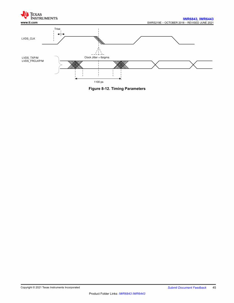
Trise
LVDS_CLK
LVDS_TXP/M
LVDS_FRCLKP/M
1100 ps
Clock Jitter = 6sigma
Figure 8-12. Timing Parameters
www.ti.comIWR6843, IWR6443
SWRS219E – OCTOBER 2018 – REVISED JUNE 2021
Copyright © 2021 Texas Instruments Incorporated Submit Document Feedback 45
Product Folder Links: IWR6843 IWR6443
8.10.5 General-Purpose Input/Output
Section 8.10.5.1 lists the switching characteristics of output timing relative to load capacitance.
8.10.5.1 Switching Characteristics for Output Timing versus Load Capacitance (CL)(1) (2)
PARAMETER TEST CONDITIONS VIOIN = 1.8V VIOIN = 3.3V UNIT
tr Max rise time
Slew control = 0
CL = 20 pF 2.8 3.0
nsCL = 50 pF 6.4 6.9
CL = 75 pF 9.4 10.2
tf Max fall time
CL = 20 pF 2.8 2.8
nsCL = 50 pF 6.4 6.6
CL = 75 pF 9.4 9.8
tr Max rise time
Slew control = 1
CL = 20 pF 3.3 3.3
nsCL = 50 pF 6.7 7.2
CL = 75 pF 9.6 10.5
tf Max fall time
CL = 20 pF 3.1 3.1
nsCL = 50 pF 6.6 6.6
CL = 75 pF 9.6 9.6
(1) Slew control, which is configured by PADxx_CFG_REG, changes behavior of the output driver (faster or slower output slew rate).(2) The rise/fall time is measured as the time taken by the signal to transition from 10% and 90% of VIOIN voltage.
IWR6843, IWR6443SWRS219E – OCTOBER 2018 – REVISED JUNE 2021 www.ti.com
46 Submit Document Feedback Copyright © 2021 Texas Instruments Incorporated
Product Folder Links: IWR6843 IWR6443
8.10.6 Controller Area Network - Flexible Data-rate (CAN-FD)
The CAN-FD module supports both classic CAN and CAN FD (CAN with Flexible Data-Rate) specifications. CAN FD feature allows high throughput and increased payload per data frame. The classic CAN and CAN FD devices can coexist on the same network without any conflict.
The CAN-FD has the following features:
• Conforms with CAN Protocol 2.0 A, B and ISO 11898-1• Full CAN FD support (up to 64 data bytes per frame)• AUTOSAR and SAE J1939 support• Up to 32 dedicated Transmit Buffers• Configurable Transmit FIFO, up to 32 elements• Configurable Transmit Queue, up to 32 elements• Configurable Transmit Event FIFO, up to 32 elements• Up to 64 dedicated Receive Buffers• Two configurable Receive FIFOs, up to 64 elements each• Up to 128 11-bit filter elements• Internal Loopback mode for self-test• Mask-able interrupts, two interrupt lines• Two clock domains (CAN clock / Host clock)• Parity / ECC support - Message RAM single error correction and double error detection (SECDED)
mechanism• Full Message Memory capacity (4352 words).
8.10.6.1 Dynamic Characteristics for the CANx TX and RX Pins
PARAMETER MIN TYP MAX UNITtd(CAN_FD_tx) Delay time, transmit shift register to CAN_FD_tx
pin(1) 15 ns
td(CAN_FD_rx) Delay time, CAN_FD_rx pin to receive shift register(1) 10 ns
(1) These values do not include rise/fall times of the output buffer.
8.10.7 Serial Communication Interface (SCI)
The SCI has the following features:
• Standard universal asynchronous receiver-transmitter (UART) communication• Standard non-return to zero (NRZ) format• Double-buffered receive and transmit functions• Asynchronous or iso-synchronous communication modes with no CLK pin• Capability to use Direct Memory Access (DMA) for transmit and receive data• Two external pins: RS232_RX and RS232_TX
8.10.7.1 SCI Timing Requirements
MIN TYP MAX UNITf(baud) Supported baud rate at 20 pF 921.6 kHz
www.ti.comIWR6843, IWR6443
SWRS219E – OCTOBER 2018 – REVISED JUNE 2021
Copyright © 2021 Texas Instruments Incorporated Submit Document Feedback 47
Product Folder Links: IWR6843 IWR6443
8.10.8 Inter-Integrated Circuit Interface (I2C)
The inter-integrated circuit (I2C) module is a multimaster communication module providing an interface between devices compliant with Philips Semiconductor I2C-bus specification version 2.1 and connected by an I2C-bus™. This module will support any slave or master I2C compatible device.
The I2C has the following features:
• Compliance to the Philips I2C bus specification, v2.1 (The I2C Specification, Philips document number 9398 393 40011)– Bit/Byte format transfer– 7-bit and 10-bit device addressing modes– General call– START byte– Multi-master transmitter/ slave receiver mode– Multi-master receiver/ slave transmitter mode– Combined master transmit/receive and receive/transmit mode– Transfer rates of 100 kbps up to 400 kbps (Phillips fast-mode rate)
• Free data format• Two DMA events (transmit and receive)• DMA event enable/disable capability• Module enable/disable capability• The SDA and SCL are optionally configurable as general purpose I/O• Slew rate control of the outputs• Open drain control of the outputs• Programmable pullup/pulldown capability on the inputs• Supports Ignore NACK mode
Note
This I2C module does not support:• High-speed (HS) mode• C-bus compatibility mode• The combined format in 10-bit address mode (the I2C sends the slave address second byte every
time it sends the slave address first byte)
IWR6843, IWR6443SWRS219E – OCTOBER 2018 – REVISED JUNE 2021 www.ti.com
48 Submit Document Feedback Copyright © 2021 Texas Instruments Incorporated
Product Folder Links: IWR6843 IWR6443

8.10.8.1 I2C Timing Requirements(1)
STANDARD MODE FAST MODEUNIT
MIN MAX MIN MAXtc(SCL) Cycle time, SCL 10 2.5 μs
tsu(SCLH-SDAL) Setup time, SCL high before SDA low(for a repeated START condition)
4.7 0.6 μs
th(SCLL-SDAL) Hold time, SCL low after SDA low(for a START and a repeated START condition)
4 0.6 μs
tw(SCLL) Pulse duration, SCL low 4.7 1.3 μs
tw(SCLH) Pulse duration, SCL high 4 0.6 μs
tsu(SDA-SCLH) Setup time, SDA valid before SCL high 250 100 μs
th(SCLL-SDA) Hold time, SDA valid after SCL low 0 3.45(1) 0 0.9 μs
tw(SDAH) Pulse duration, SDA high between STOP and START conditions
4.7 1.3 μs
tsu(SCLH-SDAH) Setup time, SCL high before SDA high(for STOP condition)
4 0.6 μs
tw(SP) Pulse duration, spike (must be suppressed) 0 50 ns
Cb (2) (3) Capacitive load for each bus line 400 400 pF
(1) The I2C pins SDA and SCL do not feature fail-safe I/O buffers. These pins could potentially draw current when the device is powered down.
(2) The maximum th(SDA-SCLL) for I2C bus devices has only to be met if the device does not stretch the low period (tw(SCLL)) of the SCL signal.
(3) Cb = total capacitance of one bus line in pF. If mixed with fast-mode devices, faster fall-times are allowed.
SDA
SCL
tw(SDAH)
tw(SCLL)
tw(SCLH)
tw(SP)
th(SCLL-SDAL)
th(SDA-SCLL)
th(SCLL-SDAL)
tsu(SCLH-SDAL)
tf(SCL)tc(SCL)
tr(SCL)tsu(SCLH-SDAH)
Stop Start Repeated Start Stop
tsu(SDA-SCLH)
Figure 8-13. I2C Timing Diagram
Note• A device must internally provide a hold time of at least 300 ns for the SDA signal (referred to the
VIHmin of the SCL signal) to bridge the undefined region of the falling edge of SCL.• The maximum th(SDA-SCLL) has only to be met if the device does not stretch the LOW
period (tw(SCLL)) of the SCL signal. E.A Fast-mode I2C-bus device can be used in a Standard-mode I2C-bus system, but the requirement tsu(SDA-SCLH) ≥ 250 ns must then be met. This will automatically be the case if the device does not stretch the LOW period of the SCL signal. If such a device does stretch the LOW period of the SCL signal, it must output the next data bit to the SDA line tr max + tsu(SDA-SCLH).
www.ti.comIWR6843, IWR6443
SWRS219E – OCTOBER 2018 – REVISED JUNE 2021
Copyright © 2021 Texas Instruments Incorporated Submit Document Feedback 49
Product Folder Links: IWR6843 IWR6443

8.10.9 Quad Serial Peripheral Interface (QSPI)
The quad serial peripheral interface (QSPI) module is a kind of SPI module that allows single, dual, or quad read access to external SPI devices. This module has a memory mapped register interface, which provides a direct interface for accessing data from external SPI devices and thus simplifying software requirements. The QSPI works as a master only. The QSPI in the device is primarily intended for fast booting from quad-SPI flash memories.
The QSPI supports the following features:
• Programmable clock divider• Six-pin interface• Programmable length (from 1 to 128 bits) of the words transferred• Programmable number (from 1 to 4096) of the words transferred• Support for 3-, 4-, or 6-pin SPI interface• Optional interrupt generation on word or frame (number of words) completion• Programmable delay between chip select activation and output data from 0 to 3 QSPI clock cycles
Section 8.10.9.2 and Section 8.10.9.3 assume the operating conditions stated in Section 8.10.9.1.
8.10.9.1 QSPI Timing Conditions
MIN TYP MAX UNITInput Conditions
tR Input rise time 1 3 ns
tF Input fall time 1 3 ns
Output Conditions
CLOAD Output load capacitance 2 15 pF
8.10.9.2 Timing Requirements for QSPI Input (Read) Timings(1) (2)
MIN TYP MAX UNITtsu(D-SCLK) Setup time, d[3:0] valid before falling sclk edge 7.3 ns
th(SCLK-D) Hold time, d[3:0] valid after falling sclk edge 1.5 ns
tsu(D-SCLK) Setup time, final d[3:0] bit valid before final falling sclk edge 7.3 – P(3) ns
th(SCLK-D) Hold time, final d[3:0] bit valid after final falling sclk edge 1.5 + P(3) ns
(1) Clock Mode 0 (clk polarity = 0 ; clk phase = 0 ) is the mode of operation.(2) The Device captures data on the falling clock edge in Clock Mode 0, as opposed to the traditional rising clock edge. Although
non-standard, the falling-edge-based setup and hold time timings have been designed to be compatible with standard SPI devices that launch data on the falling edge in Clock Mode 0.
(3) P = SCLK period in ns.
IWR6843, IWR6443SWRS219E – OCTOBER 2018 – REVISED JUNE 2021 www.ti.com
50 Submit Document Feedback Copyright © 2021 Texas Instruments Incorporated
Product Folder Links: IWR6843 IWR6443
8.10.9.3 QSPI Switching Characteristics
NO. PARAMETER MIN TYP MAX UNITQ1 tc(SCLK) Cycle time, sclk 12.5 ns
Q2 tw(SCLKL) Pulse duration, sclk low Y*P – 3(1) (2) ns
Q3 tw(SCLKH) Pulse duration, sclk high Y*P – 3(1) ns
Q4 td(CS-SCLK) Delay time, sclk falling edge to cs active edge –M*P – 1(1) (3) –M*P + 2.5(1) (3)
ns
Q5 td(SCLK-CS) Delay time, sclk falling edge to cs inactive edge N*P – 1(1) (3) N*P + 2.5(1) (3)
ns
Q6 td(SCLK-D1) Delay time, sclk falling edge to d[1] transition –3.5 7 ns
Q7 tena(CS-D1LZ) Enable time, cs active edge to d[1] driven (lo-z) –P – 4(3) –P +1(3) ns
Q8 tdis(CS-D1Z) Disable time, cs active edge to d[1] tri-stated (hi-z) –P – 4(3) –P +1(3) ns
Q9 td(SCLK-D1) Delay time, sclk first falling edge to first d[1] transition (for PHA = 0 only) –3.5 – P(3) 7 – P(3) ns
Q12 tsu(D-SCLK) Setup time, d[3:0] valid before falling sclk edge 7.3 ns
Q13 th(SCLK-D) Hold time, d[3:0] valid after falling sclk edge 1.5 ns
Q14 tsu(D-SCLK) Setup time, final d[3:0] bit valid before final falling sclk edge 7.3 — P(3) ns
Q15 th(SCLK-D) Hold time, final d[3:0] bit valid after final falling sclk edge 1.5 + P(3) ns
(1) The Y parameter is defined as follows: If DCLK_DIV is 0 or ODD then, Y equals 0.5. If DCLK_DIV is EVEN then, Y equals (DCLK_DIV/2) / (DCLK_DIV+1). For best performance, it is recommended to use a DCLK_DIV of 0 or ODD to minimize the duty cycle distortion. All required details about clock division factor DCLK_DIV can be found in the device-specific Technical Reference Manual.
(2) P = SCLK period in ns.(3) M = QSPI_SPI_DC_REG.DDx + 1, N = 2
Figure 8-14. QSPI Read (Clock Mode 0)
www.ti.comIWR6843, IWR6443
SWRS219E – OCTOBER 2018 – REVISED JUNE 2021
Copyright © 2021 Texas Instruments Incorporated Submit Document Feedback 51
Product Folder Links: IWR6843 IWR6443
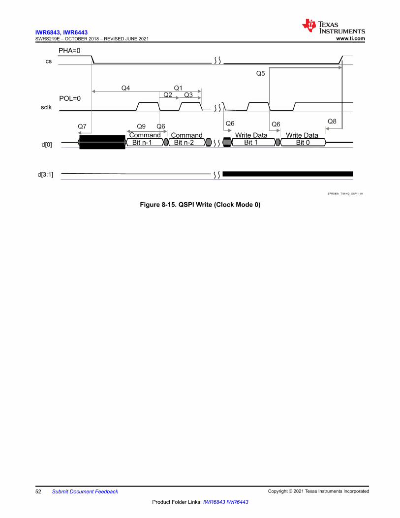
cs
sclk
d[0]
d[3:1]
Bit n-1 Bit n-2 Bit 1 Bit 0
PHA=0
POL=0
Command Command Write Data Write Data
Q4
Q7
Q2 Q3Q1
Q6 Q6
Q5
SPRS85v_TIMING_OSPI1_04
Q8Q9 Q6
Figure 8-15. QSPI Write (Clock Mode 0)
IWR6843, IWR6443SWRS219E – OCTOBER 2018 – REVISED JUNE 2021 www.ti.com
52 Submit Document Feedback Copyright © 2021 Texas Instruments Incorporated
Product Folder Links: IWR6843 IWR6443

8.10.10 ETM Trace Interface
Section 8.10.10.2 and List item.referenceTitle assume the recommended operating conditions stated in Section 8.10.10.1.
8.10.10.1 ETMTRACE Timing Conditions
MIN TYP MAX UNITOutput Conditions
CLOAD Output load capacitance 2 20 pF
8.10.10.2 ETM TRACE Switching Characteristics
NO. PARAMETER MIN TYP MAX UNIT1 tcyc(ETM) Cycle time, TRACECLK period 20 ns
2 th(ETM) Pulse Duration, TRACECLK High 9 ns
3 tl(ETM) Pulse Duration, TRACECLK Low 9 ns
4 tr(ETM) Clock and data rise time 3.3 ns
5 tf(ETM) Clock and data fall time 3.3 ns
6td(ETMTRACECLKH-ETMDATAV)
Delay time, ETM trace clock high to ETM data valid 1 7 ns
7td(ETMTRACECLKl-ETMDATAV)
Delay time, ETM trace clock low to ETM data valid 1 7 ns
tr(ETM)
th(ETM)
tl(ETM)
tf(ETM)
tcyc(ETM)
Figure 8-16. ETMTRACECLKOUT Timing
Figure 8-17. ETMDATA Timing
www.ti.comIWR6843, IWR6443
SWRS219E – OCTOBER 2018 – REVISED JUNE 2021
Copyright © 2021 Texas Instruments Incorporated Submit Document Feedback 53
Product Folder Links: IWR6843 IWR6443

8.10.11 Data Modification Module (DMM)
A Data Modification Module (DMM) gives the ability to write external data into the device memory.
The DMM has the following features:
• Acts as a bus master, thus enabling direct writes to the 4GB address space without CPU intervention• Writes to memory locations specified in the received packet (leverages packets defined by trace mode of the
RAM trace port [RTP] module)• Writes received data to consecutive addresses, which are specified by the DMM (leverages packets defined
by direct data mode of RTP module)• Configurable port width (1, 2, 4, 8 pins)• Up to 100 Mbit/s pin data rate
8.10.11.1 DMM Timing Requirements
MIN TYP MAX UNITtcyc(DMM) Clock period 10 ns
tR Clock rise time 1 3 ns
tF Clock fall time 1 3 ns
th(DMM) High pulse width 6 ns
tl(DMM) Low pulse width 6 ns
tssu(DMM) SYNC active to clk falling edge setup time 2 ns
tsh(DMM) DMM clk falling edge to SYNC deactive hold time 3 ns
tdsu(DMM) DATA to DMM clk falling edge setup time 2 ns
tdh(DMM) DMM clk falling edge to DATA hold time 3 ns
tcyc(DMM)
tr tfth(DMM)
tl(DMM)
Figure 8-18. DMMCLK Timing
DMMSYNC
DMMCLK
DMMDATA
tssu(DMM) tsh(DMM)
tdsu(DMM) tdh(DMM)
Figure 8-19. DMMDATA Timing
IWR6843, IWR6443SWRS219E – OCTOBER 2018 – REVISED JUNE 2021 www.ti.com
54 Submit Document Feedback Copyright © 2021 Texas Instruments Incorporated
Product Folder Links: IWR6843 IWR6443

8.10.12 JTAG Interface
Section 8.10.12.2 and Section 8.10.12.3 assume the operating conditions stated in Section 8.10.12.1.
8.10.12.1 JTAG Timing Conditions
MIN TYP MAX UNITInput Conditions
tR Input rise time 1 3 ns
tF Input fall time 1 3 ns
Output Conditions
CLOAD Output load capacitance 2 15 pF
8.10.12.2 Timing Requirements for IEEE 1149.1 JTAG
NO. MIN TYP MAX UNIT1 tc(TCK) Cycle time TCK 66.66 ns
1a tw(TCKH) Pulse duration TCK high (40% of tc) 26.67 ns
1b tw(TCKL) Pulse duration TCK low(40% of tc) 26.67 ns
3tsu(TDI-TCK) Input setup time TDI valid to TCK high 2.5 ns
tsu(TMS-TCK) Input setup time TMS valid to TCK high 2.5 ns
4th(TCK-TDI) Input hold time TDI valid from TCK high 18 ns
th(TCK-TMS) Input hold time TMS valid from TCK high 18 ns
8.10.12.3 Switching Characteristics Over Recommended Operating Conditions for IEEE 1149.1 JTAG
NO. PARAMETER MIN TYP MAX UNIT2 td(TCKL-TDOV) Delay time, TCK low to TDO valid 0 25 ns
3
TCK
TDO
TDI/TMS
2
4
11a 1b
SPRS91v_JTAG_01
Figure 8-20. JTAG Timing
www.ti.comIWR6843, IWR6443
SWRS219E – OCTOBER 2018 – REVISED JUNE 2021
Copyright © 2021 Texas Instruments Incorporated Submit Document Feedback 55
Product Folder Links: IWR6843 IWR6443

9 Detailed Description9.1 OverviewThe IWR6843 device includes the entire Millimeter Wave blocks and analog baseband signal chain for three transmitters and four receivers, as well as a customer-programmable MCU and DSP. This device is applicable as a radar-on-a-chip in use-cases with modest requirements for memory, processing capacity and application code size. These could be cost-sensitive industrial radar sensing applications. Examples are:• Industrial-level sensing• Industrial automation sensor fusion with radar• Traffic intersection monitoring with radar• Industrial radar-proximity monitoring• People counting• Gesturing
In terms of scalability, the IWR6843 device could be paired with a low-end external MCU, to address more complex applications that might require additional memory for a larger application software footprint and faster interfaces. The IWR6843 has an embedded DSP for signal processing, processing the radar signals for FFT, magnitude, detection, and other applications.
9.2 Functional Block Diagram
IF ADC
Digital
Front-End
(Decimation
Filter Chain)
LNA
IF ADCLNA
IF ADCLNA
IF ADCLNA
PA ´Å
PA ´ÅSynth
(20 GHz)
Ramp
Generatorx3
Osc.
Radio (BIST)
Processor
(For RF Calibration
& Self-Test ±�TI
Programmed)
Prog RAM & ROM
Data RAM
GPADC
Temp
Cortex R4F
@ 200MHz
(User Programmable)
Prog RAM(512kB)
Data RAM(192kB)
Boot ROM
QSPI
SPI
SPI / I2C
UARTs
DMA
Test/
DebugADC
Buffer
LVDS
RF/Analog Sub-System
Radio Processor
Sub-System(TI Programmed)
Main Sub-System(Customer Programmed)
Serial Flash Interface
Optional External
MCU Interface
PMIC Control
CAN-FD Communication
JTAG For Debug/
Development
High-Speed ADC Output
Interface (For Recording)
6
CAN-FD
DSP Sub-System(Customer Programmed)
Mailbox
Bus M
atr
ix
HILHigh-Speed Input For
Hardware-In-Loop Verification
C674x DSP
@ 600 MHz
(IWR6843 ONLY)
L1P (32kB)
L1D (32kB)
L2 (256kB)
DMA CRCRadar Data Memory
768 kB
PA ´Å
Radar Hardware Accelerator
(FFT, Log Mag, And Others)
Figure 9-1. Functional Block Diagram
IWR6843, IWR6443SWRS219E – OCTOBER 2018 – REVISED JUNE 2021 www.ti.com
56 Submit Document Feedback Copyright © 2021 Texas Instruments Incorporated
Product Folder Links: IWR6843 IWR6443
9.3 Subsystems9.3.1 RF and Analog Subsystem
The RF and analog subsystem includes the RF and analog circuitry – namely, the synthesizer, PA, LNA, mixer, IF, and ADC. This subsystem also includes the crystal oscillator and temperature sensors. The three transmit channels can be operated up to a maximum of two at a time (simultaneously) in 1.3-V mode. The three Transmit channels simultaneous operation is supported only with 1-V LDO bypass and PA LDO disabled mode for transmit beamforming purpose, as required. In this mode, the 1-V supply needs to be fed on the VIN_13RF1, VIN_13RF2, and VOUT PA pin; whereas, the four receive channels can all be operated simultaneously.
www.ti.comIWR6843, IWR6443
SWRS219E – OCTOBER 2018 – REVISED JUNE 2021
Copyright © 2021 Texas Instruments Incorporated Submit Document Feedback 57
Product Folder Links: IWR6843 IWR6443

9.3.1.1 Clock Subsystem
The IWR6843 clock subsystem generates 60 to 64 GHz from an input reference of 40-MHz crystal. It has a built-in oscillator circuit followed by a clean-up PLL and a RF synthesizer circuit. The output of the RF synthesizer is then processed by an X3 multiplier to create the required frequency in the 60 to 64 GHz spectrum. The RF synthesizer output is modulated by the timing engine block to create the required waveforms for effective sensor operation.
The clean-up PLL also provides a reference clock for the host processor after system wakeup.
The clock subsystem also has built-in mechanisms for detecting the presence of a crystal and monitoring the quality of the generated clock.
Figure 9-2 describes the clock subsystem.
Clean-Up
PLL
x3 MULT
RFSYNTH
Timing EngineRX LO
XO / Slicer
SoC
Clock
40 MHz
CLK Detect
Lock Detect
SYNC_IN
OSC_CLKOUT
Lo
ck D
ete
ct
TX LO
SYNC_OUT
PA
En
ve
lop
e
TX
Ph
ase
Mo
d.
AD
CsSelf Test
Figure 9-2. Clock Subsystem
IWR6843, IWR6443SWRS219E – OCTOBER 2018 – REVISED JUNE 2021 www.ti.com
58 Submit Document Feedback Copyright © 2021 Texas Instruments Incorporated
Product Folder Links: IWR6843 IWR6443

9.3.1.2 Transmit Subsystem
The IWR6843 transmit subsystem consists of three parallel transmit chains, each with independent phase and amplitude control. The device supports 6-bit linear phase modulation for MIMO radar, Tx Beam forming applications, and interference mitigation.
The transmit chains also support programmable backoff for system optimization.
Figure 9-3 describes the transmit subsystem.
Chip
Self TestLoopback
pathP
ackage
PCB
50 WDF LO
6-bit Linear PhaseShifter
0 or 180°(From timing Engine)
Figure 9-3. Transmit Subsystem (Per Channel)
9.3.1.3 Receive Subsystem
The IWR6843 receive subsystem consists of four parallel channels. A single receive channel consists of an LNA, mixer, IF filtering, ADC conversion, and decimation. All four receive channels can be operational at the same time an individual power-down option is also available for system optimization.
Unlike conventional real-only receivers, the IWR6843 device supports a complex baseband architecture, which uses quadrature mixer and dual IF and ADC chains to provide complex I and Q outputs for each receiver channel. The IWR6843 is targeted for fast chirp systems. The band-pass IF chain has configurable lower cutoff frequencies above 175 kHz and can support bandwidths up to 10 MHz.
Figure 9-4 describes the receive subsystem.
Self Test
Ch
ip
Pa
cka
ge
PCB
50 W
GSG
LoopbackPath
DAC
DSM
DSM
RSSII
Q
LO
Sa
tura
tio
nD
ete
ct
DAC
De
cim
atio
n
Ima
ge
Re
jectio
n
AD
C B
uffe
r
I/Q
Co
rre
ctio
n
Figure 9-4. Receive Subsystem (Per Channel)
www.ti.comIWR6843, IWR6443
SWRS219E – OCTOBER 2018 – REVISED JUNE 2021
Copyright © 2021 Texas Instruments Incorporated Submit Document Feedback 59
Product Folder Links: IWR6843 IWR6443

9.3.2 Processor Subsystem
DSP/HWA Interconnect ± 128 bit @ 200 MHz Main Interconnect
Interconnect
ADC Buffer
L3
Data
Handshake
Memory
CRC
LVDS
DSP
L2
EDMA
MSS
DMA
HIL JTAG CRC HIL
Main
R4F
ROM
TCM A
TCM B
L1P
L1d
Box
SPIUART I2C QSPI CAN-FD
PWM,
PMICCLK
BSS Interconnect
Unified
128 KB x 2
32 KB Ping-Pong32 KB
32 KB
32 KB
192 KB
512 KB
Cache/
RAM
(static sharing
with R4F Space)
HWA
Figure 9-5. Processor Subsystem
Figure 9-5 shows the block diagram for customer programmable processor subsystems in the IWR6843 device. At a high level there are two customer programmable subsystems, as shown separated by a dotted line in the diagram. Left hand side shows the DSP Subsystem which contains TI's high-performance C674x DSP(IWR6843 only), hardware accelerator, a high-bandwidth interconnect for high performance (128-bit, 200MHz), and associated peripherals – four DMAs for data transfer. LVDS interface for Measurement data output, L3 Radar data cube memory, ADC buffers, CRC engine, and data handshake memory (additional memory provided on interconnect).
The C674x DSP and L1/L2 RAM portion of the DSP subsystem is not supported on the IWR6443 device and therefore, the available memory is 1.4MB compared to 1.75MB on the IWR6843 device. For more information on the features supported and not supported on each device, see the Device Features Comparison table.
The right side of the diagram shows the Main subsystem. Main subsystem as name suggests is the brain of the device and controls all the device peripherals and house-keeping activities of the device. Main subsystem contains Cortex-R4F (Main R4F) processor and associated peripherals and house-keeping components such as DMAs, CRC and Peripherals (I2C, UART, SPIs, CAN, PMIC clocking module, PWM, and others) connected to Main Interconnect through Peripheral Central Resource (PCR interconnect).
Details of the DSP CPU core can be found at https://www.ti.com/product/TMS320C6748.
HIL module is shown in both the subsystems and can be used to perform the radar operations feeding the captured data from outside into the device without involving the RF subsystem. HIL on Main SS is for controlling the configuration and HIL on DSPSS for high speed ADC data input to the device. Both HIL modules uses the same IOs on the device, one additional IO (DMM_MUX_IN) allows selecting either of the two.
IWR6843, IWR6443SWRS219E – OCTOBER 2018 – REVISED JUNE 2021 www.ti.com
60 Submit Document Feedback Copyright © 2021 Texas Instruments Incorporated
Product Folder Links: IWR6843 IWR6443

9.3.3 Host Interface
The host interface can be provided through a SPI, UART, or CAN-FD interface. In some cases the serial interface for industrial applications is transcoded to a different serial standard.
The IWR6843 device communicates with the host radar processor over the following main interfaces:
• Reference Clock – Reference clock available for host processor after device wakeup• Control – 4-port standard SPI (slave) for host control . All radio control commands (and response) flow
through this interface.• Reset – Active-low reset for device wakeup from host• Host Interrupt - an indication that the mmwave sensor needs host interface• Error – Used for notifying the host in case the radio controller detects a fault
9.3.4 Main Subsystem Cortex-R4F
The main system includes an Arm Cortex R4F processor, clock with a maximum operating frequency of 200 MHz. User applications executing on this processor control the overall operation of the device, including radar control through well-defined API messages, radar signal processing (assisted by the radar hardware accelerator), and peripherals for external interfaces.
See the Technical Reference Manual for a complete description and memory map.
9.3.5 DSP Subsystem
The DSP subsystem includes TI’s standard TMS320C674x megamodule and several blocks of internal memory (L1P, L1D, and L2). For complete information including memory map, please refer to Technical Reference Manual.
9.3.6 Hardware Accelerator
The Radar Hardware Accelerator (HWA) is an IP that enables off-loading the burden of certain frequently used computations in FMCW radar signal processing from the main processor. FMCW radar signal processing involves the use of FFT and Log-Magnitude computations to obtain a radar image across the range, velocity, and angle dimensions. Some of the frequently used functions in FMCW radar signal processing can be done within the radar hardware accelerator, while still retaining the flexibility of implementing other proprietary algorithms in the main processor. See the Radar Hardware Accelerator User's Guide for a functional description and features of this module and see the Technical Reference Manual for a complete list of register and memory map.
9.4 Other Subsystems9.4.1 ADC Channels (Service) for User Application
The IWR6843 device includes provision for an ADC service for user application, where the
GPADC engine present inside the device can be used to measure up to six external voltages. The ADC1, ADC2, ADC3, ADC4, ADC5, and ADC6 pins are used for this purpose.
• ADC itself is controlled by TI firmware running inside the BIST subsystem and access to it for customer’s external voltage monitoring purpose is via ‘monitoring API’ calls routed to the BIST subsystem. This API could be linked with the user application running on MSS R4F.
• BIST subsystem firmware will internally schedule these measurements along with other RF and Analog monitoring operations. The API allows configuring the settling time (number of ADC samples to skip) and number of consecutive samples to take. At the end of a frame, the minimum, maximum and average of the readings will be reported for each of the monitored voltages.
GPADC Specifications:
• 625 Ksps SAR ADC• 0 to 1.8V input range• 10-bit resolution
www.ti.comIWR6843, IWR6443
SWRS219E – OCTOBER 2018 – REVISED JUNE 2021
Copyright © 2021 Texas Instruments Incorporated Submit Document Feedback 61
Product Folder Links: IWR6843 IWR6443

• For 5 out of the 6 inputs, an optional internal buffer (0.4-1.4V input range) is available. Without the buffer, the ADC has a switched capacitor input load modeled with 5pF of sampling capacitance and 12pF parasitic capacitance (GPADC channel 6, the internal buffer is not available).
GPADCANALOG TEST 1-4,
ANAMUX
VSENSE
5
5
A. GPADC structures are used for measuring the output of internal temperature sensors. The accuracy of these measurements is ±7°C.
Figure 9-6. ADC Path
9.4.1.1 GP-ADC Parameter
PARAMETER TYP UNITADC supply 1.8 V
ADC unbuffered input voltage range 0 – 1.8 V
ADC buffered input voltage range(1) 0.4 – 1.3 V
ADC resolution 10 bits
ADC offset error ±5 LSB
ADC gain error ±5 LSB
ADC DNL –1/+2.5 LSB
ADC INL ±2.5 LSB
ADC sample rate(2) 625 Ksps
ADC sampling time(2) 400 ns
ADC internal cap 10 pF
ADC buffer input capacitance 2 pF
ADC input leakage current 3 uA
(1) Outside of given range, the buffer output will become nonlinear.(2) ADC itself is controlled by TI firmware running inside the BIST subsystem. For more details please refer to the API calls.
IWR6843, IWR6443SWRS219E – OCTOBER 2018 – REVISED JUNE 2021 www.ti.com
62 Submit Document Feedback Copyright © 2021 Texas Instruments Incorporated
Product Folder Links: IWR6843 IWR6443
10 Monitoring and Diagnostics10.1 Monitoring and Diagnostic MechanismsTable 10-1 is a list of the main monitoring and diagnostic mechanisms available in the Functional Safety-Compliant devices
Table 10-1. Monitoring and Diagnostic Mechanisms for Functional Safety-Compliant DevicesNO FEATURE DESCRIPTION
1Boot time LBIST For MSS R4F Core and associated VIM
Device architecture supports hardware logic BIST (LBIST) engine self-test Controller (STC). This logic is used to provide a very high diagnostic coverage (>90%) on the MSS R4F CPU core and Vectored Interrupt Module (VIM) at a transistor level.LBIST for the CPU and VIM need to be triggered by application code before starting the functional safety application. CPU stays there in while loop and does not proceed further if a fault is identified.
2 Boot time PBIST for MSS R4F TCM Memories
MSS R4F has three Tightly coupled Memories (TCM) memories TCMA, TCMB0 and TCMB1. Device architecture supports a hardware programmable memory BIST (PBIST) engine. This logic is used to provide a very high diagnostic coverage (March-13n) on the implemented MSS R4F TCMs at a transistor level.PBIST for TCM memories is triggered by Bootloader at the boot time before starting download of application from Flash or peripheral interface. CPU stays there in while loop and does not proceed further if a fault is identified.
3 End to End ECC for MSS R4F TCM Memories
TCMs diagnostic is supported by Single error correction double error detection (SECDED) ECC diagnostic. An 8-bit code word is used to store the ECC data as calculated over the 64-bit data bus. ECC evaluation is done by the ECC control logic inside the CPU. This scheme provides end-to-end diagnostics on the transmissions between CPU and TCM. CPU can be configured to have predetermined response (Ignore or Abort generation) to single and double bit error conditions.
4 MSS R4F TCM bit multiplexing
Logical TCM word and its associated ECC code is split and stored in two physical SRAM banks. This scheme provides an inherent diagnostic mechanism for address decode failures in the physical SRAM banks. Faults in the bank addressing are detected by the CPU as an ECC fault.Further, bit multiplexing scheme implemented such that the bits accessed to generate a logical (CPU) word are not physically adjacent. This scheme helps to reduce the probability of physical multi-bit faults resulting in logical multi-bit faults; rather they manifest as multiple single bit faults. As the SECDED TCM ECC can correct a single bit fault in a logical word, this scheme improves the usefulness of the TCM ECC diagnostic.Both these features are hardware features and cannot be enabled or disabled by application software.
5 Clock Monitor
Device architecture supports Three Digital Clock Comparators (DCCs) and an internal RCOSC. Dual functionality is provided by these modules – Clock detection and Clock Monitoring.DCCint is used to check the availability/range of Reference clock at boot otherwise the device is moved into limp mode (Device still boots but on 10MHz RCOSC clock source. This provides debug capability). DCCint is only used by boot loader during boot time. It is disabled once the APLL is enabled and locked.DCC1 is dedicated for APLL lock detection monitoring, comparing the APLL output divided version with the Reference input clock of the device. Initially (before configuring APLL), DCC1 is used by bootloader to identify the precise frequency of reference input clock against the internal RCOSC clock source. Failure detection for DCC1 would cause the device to go into limp mode.DCC2 module is one which is available for user software . From the list of clock options given in detailed spec, any two clocks can be compared. One example usage is to compare the CPU clock with the Reference or internal RCOSC clock source. Failure detection is indicated to the MSS R4F CPU via Error Signaling Module (ESM).
7 RTI/WD for MSS R4F
Device architecture supports the use of an internal watchdog that is implemented in the real-time interrupt (RTI) module. The internal watchdog has two modes of operation: digital watchdog (DWD) and digital windowed watchdog (DWWD). The modes of operation are mutually exclusive; the designer can elect to use one mode or the other but not both at the same time.Watchdog can issue either an internal (warm) system reset or a CPU non-mask able interrupt upon detection of a failure.The Watchdog is enabled by the bootloader in DWD mode at boot time to track the boot process. Once the application code takes up the control, Watchdog can be configured again for mode and timings based on specific customer requirements.
www.ti.comIWR6843, IWR6443
SWRS219E – OCTOBER 2018 – REVISED JUNE 2021
Copyright © 2021 Texas Instruments Incorporated Submit Document Feedback 63
Product Folder Links: IWR6843 IWR6443
Table 10-1. Monitoring and Diagnostic Mechanisms for Functional Safety-Compliant Devices (continued)NO FEATURE DESCRIPTION
8 MPU for MSS R4F
Cortex-R4F CPU includes an MPU. The MPU logic can be used to provide spatial separation of software tasks in the device memory. Cortex-R4F MPU supports 12 regions. It is expected that the operating system controls the MPU and changes the MPU settings based on the needs of each task. A violation of a configured memory protection policy results in a CPU abort.
9 PBIST for Peripheral interface SRAMs - SPIs, CANs
Device architecture supports a hardware programmable memory BIST (PBIST) engine for Peripheral SRAMs as well.PBIST for peripheral SRAM memories can be triggered by the application. User can elect to run the PBIST on one SRAM or on groups of SRAMs based on the execution time, which can be allocated to the PBIST diagnostic. The PBIST tests are destructive to memory contents, and as such are typically run only at boot time. However, the user has the freedom to initiate the tests at any time if peripheral communication can be hindered.Any fault detected by the PBIST results in an error indicated in PBIST status registers.
10 ECC for Peripheral interface SRAMs – SPIs, CANs
Peripheral interface SRAMs diagnostic is supported by Single error correction double error detection (SECDED) ECC diagnostic. When a single or double bit error is detected the MSS R4F is notified via ESM (Error Signaling Module). This feature is disabled after reset. Software must configure and enable this feature in the peripheral and ESM module. ECC failure (both single bit corrected and double bit uncorrectable error conditions) is reported to the MSS R4F as an interrupt via ESM module.
11Configuration registers protection for Main SS peripherals
All the Main SS peripherals (SPIs, CANs, I2C, DMAs, RTI/WD, DCCs, IOMUX etc.) are connected to interconnect via Peripheral Central resource (PCR). This provides two diagnostic mechanisms that can limit access to peripherals. Peripherals can be clock gated per peripheral chip select in the PCR. This can be utilized to disable unused features such that they cannot interfere. In addition, each peripheral chip select can be programmed to limit access based on privilege level of transaction. This feature can be used to limit access to entire peripherals to privileged operating system code only.These diagnostic mechanisms are disabled after reset. Software must configure and enable these mechanisms. Protection violation also generates an ‘error’ that result in abort to MSS R4F or error response to other peripherals such as DMAs.
12 Cyclic Redundancy Check –Main SS
Device architecture supports hardware CRC engine on Main SS implementing the below polynomials.• CRC16 CCITT – 0x10• CRC32 Ethernet – 0x04C11DB7• CRC64• CRC 32C – CASTAGNOLI – 0x1EDC6F4• CRC32P4 – E2E Profile4 – 0xF4ACFB1• CRC-8 – H2F Autosar – 0x2F• CRC-8 – VDA CAN – 0x1D
The read operation of the SRAM contents to the CRC can be done by CPU or by DMA. The comparison of results, indication of fault, and fault response are the responsibility of the software managing the test.
13 MPU for DMAs
Device architecture supports MPUs on Main SS DMAs. Failure detection by MPU is reported to the MSS R4F CPU core as an interrupt via ESM.DSPSS’s high performance EDMAs also includes MPUs on both read and write ports. EDMA MPUs supports 8 regions. Failure detection by MPU is reported to the DSP core as an interrupt via local ESM.
14Boot time LBIST For BIST R4F Core and associated VIM
Device architecture supports hardware logic BIST (LBIST) even for BIST R4F core and associated VIM module. This logic provides very high diagnostic coverage (>90%) on the BIST R4F CPU core and VIM.This is triggered by MSS R4F boot loader at boot time and it does not proceed further if the fault is detected.
15 Boot time PBIST for BIST R4F TCM Memories
Device architecture supports a hardware programmable memory BIST (PBIST) engine for BIST R4F TCMs which provide a very high diagnostic coverage (March-13n) on the BIST R4F TCMs.PBIST is triggered by MSS R4F Bootloader at the boot time and it does not proceed further if the fault is detected.
16 End to End ECC for BIST R4F TCM Memories
BIST R4F TCMs diagnostic is supported by Single error correction double error detection (SECDED) ECC diagnostic. Single bit error is communicated to the BIST R4FCPU while double bit error is communicated to MSS R4F as an interrupt so that application code becomes aware of this and takes appropriate action.
IWR6843, IWR6443SWRS219E – OCTOBER 2018 – REVISED JUNE 2021 www.ti.com
64 Submit Document Feedback Copyright © 2021 Texas Instruments Incorporated
Product Folder Links: IWR6843 IWR6443
Table 10-1. Monitoring and Diagnostic Mechanisms for Functional Safety-Compliant Devices (continued)NO FEATURE DESCRIPTION
17 BIST R4F TCM bit multiplexing
Logical TCM word and its associated ECC code is split and stored in two physical SRAM banks. This scheme provides an inherent diagnostic mechanism for address decode failures in the physical SRAM banks and helps to reduce the probability of physical multi-bit faults resulting in logical multi-bit faults.
18 RTI/WD for BIST R4FDevice architecture supports an internal watchdog for BIST R4F. Timeout condition is reported via an interrupt to MSS R4F and rest is left to application code to either go for SW reset for BIST SS or warm reset for the device to come out of faulty condition.
19 Boot time PBIST for L1P, L1D, L2 and L3 Memories
Device architecture supports a hardware programmable memory BIST (PBIST) engine for DSPSS’s L1P, L1D, L2 and L3 memories which provide a very high diagnostic coverage (March-13n).PBIST is triggered by MSS R4F Bootloader at the boot time and it does not proceed further if the fault is detected.
20 Parity on L1P
Device architecture supports Parity diagnostic on DSP’s L1P memory. Parity error is reported to the CPU as an interrupt.Note:- L1D memory is not covered by parity or ECC and need to be covered by application level diagnostics.
21 ECC on DSP’s L2 Memory
Device architecture supports both Parity Single error correction double error detection (SECDED) ECC diagnostic on DSP’s L2 memory. L2 Memory is a unified 256KB of memory used to store program and Data sections for the DSP. A 12-bit code word is used to store the ECC data as calculated over the 256-bit data bus (logical instruction fetch size). The ECC logic for the L2 access is located in the DSP and evaluation is done by the ECC control logic inside the DSP. This scheme provides end-to-end diagnostics on the transmissions between DSP and L2. Byte aligned Parity mechanism is also available on L2 to take care of data section.
22 ECC on Radar Data Cube (L3) Memory
L3 memory is used as Radar data section in Device. Device architecture supports Single error correction double error detection (SECDED) ECC diagnostic on L3 memory. An 8-bit code word is used to store the ECC data as calculated over the 64-bit data bus.Failure detection by ECC logic is reported to the MSS R4F CPU core as an interrupt via ESM.
23 RTI/WD for DSP Core
Device architecture supports the use of an internal watchdog for BIST R4F that is implemented in the real-time interrupt (RTI) module – replication of same module as used in Main SS. This module supports same features as that of RTI/WD for MSS/BIST R4F.This watchdog is enabled by customer application code and Timeout condition is reported via an interrupt to MSS R4F and rest is left to application code in MSS R4F to either go for SW reset for DSP SS or warm reset for the device to come out of faulty condition.
24 CRC for DSP Sub-System
Device architecture supports dedicated hardware CRC on DSPSS implementing the below polynomials.• CRC16 CCITT - 0x10• CRC32 Ethernet - 0x04C11DB7• CRC64
The read of SRAM contents to the CRC can be done by DSP CPU or by DMA. The comparison of results, indication of fault, and fault response are the responsibility of the software managing the test.
25 MPU for DSPDevice architecture supports MPUs for DSP memory accesses (L1D, L1P, and L2). L2 memory supports 64 regions and 16 regions for L1P and L1D each. Failure detection by MPU is reported to the DSP core as an abort.
26 Temperature SensorsDevice architecture supports various temperature sensors all across the device (next to power hungry modules such as PAs, DSP etc) which is monitored during the inter-frame period.(1)
27 Tx Power Monitors Device architecture supports power detectors at the Tx output.(2)
28 Error SignalingError Output
When a diagnostic detects a fault, the error must be indicated. The device architecture provides aggregation of fault indication from internal monitoring/diagnostic mechanisms using a peripheral logic known as the Error Signaling Module (ESM). The ESM provides mechanisms to classify errors by severity and to provide programmable error response.ESM module is configured by customer application code and specific error signals can be enabled or masked to generate an interrupt (Low/High priority) for the MSS R4F CPU.device supports Nerror output signal (IO) which can be monitored externally to identify any kind of high severity faults in the design which could not be handled by the R4F.
www.ti.comIWR6843, IWR6443
SWRS219E – OCTOBER 2018 – REVISED JUNE 2021
Copyright © 2021 Texas Instruments Incorporated Submit Document Feedback 65
Product Folder Links: IWR6843 IWR6443

Table 10-1. Monitoring and Diagnostic Mechanisms for Functional Safety-Compliant Devices (continued)NO FEATURE DESCRIPTION
29 Synthesizer (Chirp) frequency monitor
Monitors Synthesizer’s frequency ramp by counting (divided-down) clock cycles and comparing to ideal frequency ramp. Excess frequency errors above a certain threshold, if any, are detected and reported.
30 Ball break detection for TX ports (TX Ball break monitor)
Device architecture supports a ball break detection mechanism based on Impedance measurement at the TX output(s) to detect and report any large deviations that can indicate a ball break.Monitoring is done by TIs code running on BIST R4F and failure is reported to the MSS R4F via Mailbox.It is completely up to customer SW to decide on the appropriate action based on the message from BIST R4F.
31 RX loopback test Built-in TX to RX loopback to enable detection of failures in the RX path(s), including Gain, inter-RX balance, etc.
32 IF loopback test Built-in IF (square wave) test tone input to monitor IF filter’s frequency response and detect failure.
33 RX saturation detect Provision to detect ADC saturation due to excessive incoming signal level and/or interference.
34 Boot time LBIST for DSP core Device supports boot time LBIST for the DSP Core. LBIST can be triggered by the MSS R4F application code during boot time.
(1) Monitoring is done by TI's code running on BIST R4F.There are two modes in which it could be configured to report the temperature sensed via API by customer application.a. Report the temperature sensed after every N framesb. Report the condition once the temperature crosses programmed threshold.
It is completely up to customer SW to decide on the appropriate action based on the message from BIST R4Fvia Mailbox.(2) Monitoring is done by the TI's code running on BIST R4F.
There are two modes in which it could be configured to report the detected output power via API by customer application.a. Report the power detected after every N framesb. Report the condition once the output power degrades by more than configured threshold from the configured.
It is completely up to customer SW to decide on the appropriate action based on the message from BIST R4F.
IWR6843, IWR6443SWRS219E – OCTOBER 2018 – REVISED JUNE 2021 www.ti.com
66 Submit Document Feedback Copyright © 2021 Texas Instruments Incorporated
Product Folder Links: IWR6843 IWR6443
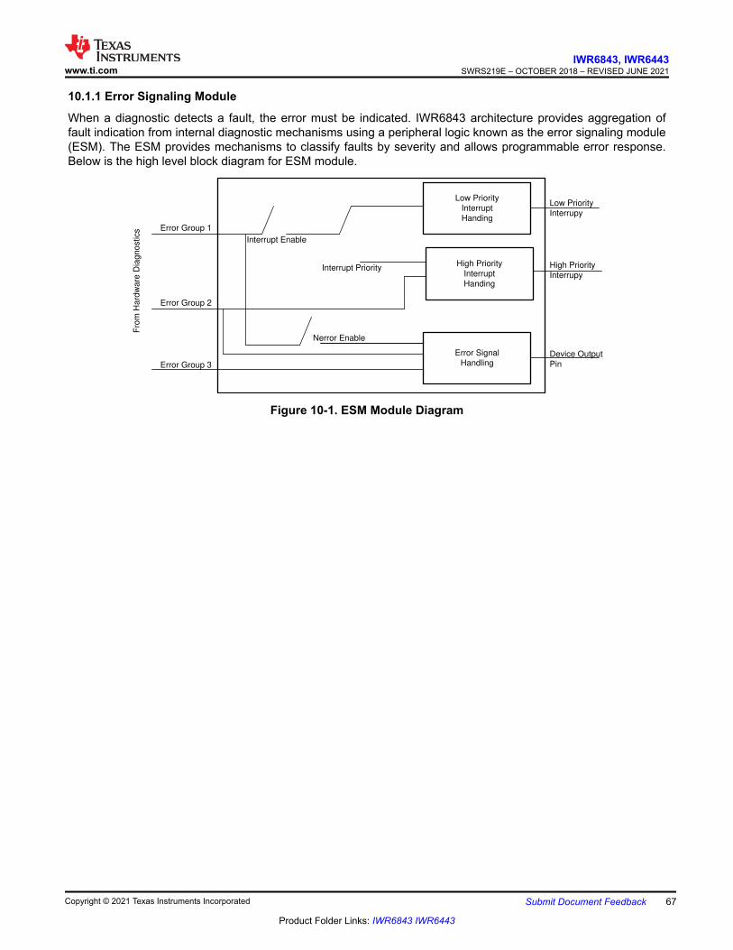
10.1.1 Error Signaling Module
When a diagnostic detects a fault, the error must be indicated. IWR6843 architecture provides aggregation of fault indication from internal diagnostic mechanisms using a peripheral logic known as the error signaling module (ESM). The ESM provides mechanisms to classify faults by severity and allows programmable error response. Below is the high level block diagram for ESM module.
Low Priority
Interrupt
Handing
High Priority
Interrupt
Handing
Error Signal
Handling
Error Group 1
Error Group 2
Error Group 3
Low Priority
Interrupy
High Priority
Interrupy
Device Output
Pin
Interrupt Enable
Interrupt Priority
Nerror Enable
Fro
m H
ard
wa
re D
iag
no
stics
Figure 10-1. ESM Module Diagram
www.ti.comIWR6843, IWR6443
SWRS219E – OCTOBER 2018 – REVISED JUNE 2021
Copyright © 2021 Texas Instruments Incorporated Submit Document Feedback 67
Product Folder Links: IWR6843 IWR6443

11 Applications, Implementation, and LayoutNote
Information in the following Applications section is not part of the TI component specification, and TI does not warrant its accuracy or completeness. TI's customers are responsible for determining suitability of components for their purposes. Customers should validate and test their design implementation to confirm system functionality.
11.1 Application InformationApplication information can be found on IWR Application web page.
11.2 Reference SchematicPlease check the device product page for latest Hardware design information under Design Kits - typically, at Design & development.
Listed for convenience are: Design Files, Schematics, Layouts, and Stack up for PCB.• Altium XWR6843 EVM Design Files• XWR6843 EVM Schematic Drawing, Assembly Drawing, and Bill of Materials
IWR6843, IWR6443SWRS219E – OCTOBER 2018 – REVISED JUNE 2021 www.ti.com
68 Submit Document Feedback Copyright © 2021 Texas Instruments Incorporated
Product Folder Links: IWR6843 IWR6443

12 Device and Documentation SupportTI offers an extensive line of development tools. Tools and software to evaluate the performance of the device, generate code, and develop solutions follow.
12.1 Device NomenclatureTo designate the stages in the product development cycle, TI assigns prefixes to the part numbers of all microprocessors (MPUs) and support tools. Each device has one of three prefixes: X, P, or null (no prefix) (for example, IWR6843). Texas Instruments recommends two of three possible prefix designators for its support tools: TMDX and TMDS. These prefixes represent evolutionary stages of product development from engineering prototypes (TMDX) through fully qualified production devices and tools (TMDS).
Device development evolutionary flow:
X Experimental device that is not necessarily representative of the final device's electrical specifications and may not use production assembly flow.
P Prototype device that is not necessarily the final silicon die and may not necessarily meet final electrical specifications.
null Production version of the silicon die that is fully qualified.
Support tool development evolutionary flow:
TMDX Development-support product that has not yet completed Texas Instruments internal qualification testing.TMDS Fully-qualified development-support product.
X and P devices and TMDX development-support tools are shipped against the following disclaimer:
"Developmental product is intended for internal evaluation purposes."
Production devices and TMDS development-support tools have been characterized fully, and the quality and reliability of the device have been demonstrated fully. TI's standard warranty applies.
Predictions show that prototype devices (X or P) have a greater failure rate than the standard production devices. Texas Instruments recommends that these devices not be used in any production system because their expected end-use failure rate still is undefined. Only qualified production devices are to be used.
TI device nomenclature also includes a suffix with the device family name. This suffix indicates the package type (for example, ABL0161), the temperature range (for example, blank is the default commercial temperature range). Figure 12-1 provides a legend for reading the complete device name for any IWR6843 device.
For orderable part numbers of IWR6843 devices in the ABL0161 package types, see the Package Option Addendum of this document , the TI website (www.ti.com), or contact your TI sales representative.
For additional description of the device nomenclature markings on the die, see the IWR6843, IWR6443 Device Errata.
www.ti.comIWR6843, IWR6443
SWRS219E – OCTOBER 2018 – REVISED JUNE 2021
Copyright © 2021 Texas Instruments Incorporated Submit Document Feedback 69
Product Folder Links: IWR6843 IWR6443

Figure 12-1. Device Nomenclature
12.2 Tools and SoftwareModels
IWR6843 BSDL model Boundary scan database of testable input and output pins for IEEE 1149.1 of the specific device.
IWR6843 IBIS model IO buffer information model for the IO buffers of the device. For simulation on a circuit board, see IBIS Open Forum.
IWR6843 checklist for schematic review, layout review, bringup/wakeup
A set of steps in spreadsheet form to select system functions and pinmux options. Specific EVM schematic and layout notes to apply to customer engineering. A bringup checklist is suggested for customers.
12.3 Documentation SupportTo receive notification of documentation updates, navigate to the device product folder on ti.com. Click on Subscribe to updates to register and receive a weekly digest of any product information that has changed. For change details, review the revision history included in any revised document.
The current documentation that describes the DSP, related peripherals, and other technical collateral follows.
Errata
IWR6843, IWR6443 device errata Describes known advisories, limitations, and cautions on silicon and provides workarounds.
12.4 Support ResourcesTI E2E™ support forums are an engineer's go-to source for fast, verified answers and design help — straight from the experts. Search existing answers or ask your own question to get the quick design help you need.
Linked content is provided "AS IS" by the respective contributors. They do not constitute TI specifications and do not necessarily reflect TI's views; see TI's Terms of Use.
IWR6843, IWR6443SWRS219E – OCTOBER 2018 – REVISED JUNE 2021 www.ti.com
70 Submit Document Feedback Copyright © 2021 Texas Instruments Incorporated
Product Folder Links: IWR6843 IWR6443

12.5 TrademarksTI E2E™ is a trademark of Texas Instruments.Arm® and Cortex® are registered trademarks of ARM Limited.All trademarks are the property of their respective owners.12.6 Electrostatic Discharge Caution
This integrated circuit can be damaged by ESD. Texas Instruments recommends that all integrated circuits be handled with appropriate precautions. Failure to observe proper handling and installation procedures can cause damage.ESD damage can range from subtle performance degradation to complete device failure. Precision integrated circuits may be more susceptible to damage because very small parametric changes could cause the device not to meet its published specifications.
12.7 GlossaryTI Glossary This glossary lists and explains terms, acronyms, and definitions.
www.ti.comIWR6843, IWR6443
SWRS219E – OCTOBER 2018 – REVISED JUNE 2021
Copyright © 2021 Texas Instruments Incorporated Submit Document Feedback 71
Product Folder Links: IWR6843 IWR6443

13 Mechanical, Packaging, and Orderable Information13.1 Packaging InformationThe following pages include mechanical, packaging, and orderable information. This information is the most current data available for the designated devices. This data is subject to change without notice and revision of this document. For browser-based versions of this data sheet, refer to the left-hand navigation.
IWR6843, IWR6443SWRS219E – OCTOBER 2018 – REVISED JUNE 2021 www.ti.com
72 Submit Document Feedback Copyright © 2021 Texas Instruments Incorporated
Product Folder Links: IWR6843 IWR6443
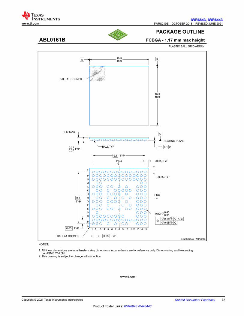
www.ti.com
PACKAGE OUTLINE
C1.17 MAX
TYP0.370.27
9.1
TYP
9.1 TYP
0.65 TYP
0.65 TYP
161X0.450.35
A10.510.3
B
10.510.3
(0.65) TYP
(0.65) TYP
FCBGA - 1.17 mm max heightABL0161BPLASTIC BALL GRID ARRAY
4223365/A 10/2016
NOTES:
1. All linear dimensions are in millimeters. Any dimensions in parenthesis are for reference only. Dimensioning and tolerancingper ASME Y14.5M.
2. This drawing is subject to change without notice.
BALL A1 CORNER
SEATING PLANE
BALL TYP 0.1 C
0.15 C A B
0.08 C
PKG
PKG
BALL A1 CORNER
R
C
D
E
F
G
H
J
K
L
M
N
P
1 2 3 4 5 6 7 8 9 10 11
A
B
12 13 14 15
SCALE 1.400
www.ti.comIWR6843, IWR6443
SWRS219E – OCTOBER 2018 – REVISED JUNE 2021
Copyright © 2021 Texas Instruments Incorporated Submit Document Feedback 73
Product Folder Links: IWR6843 IWR6443
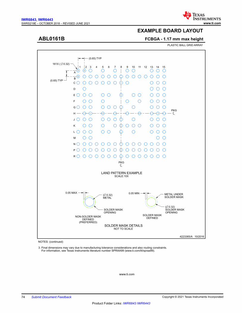
www.ti.com
EXAMPLE BOARD LAYOUT
161X ( 0.32)
(0.65) TYP
(0.65) TYP
( 0.32)METAL
0.05 MAX
SOLDER MASKOPENING
METAL UNDERSOLDER MASK
( 0.32)SOLDER MASKOPENING
0.05 MIN
FCBGA - 1.17 mm max heightABL0161BPLASTIC BALL GRID ARRAY
4223365/A 10/2016
NOTES: (continued)
3. Final dimensions may vary due to manufacturing tolerance considerations and also routing constraints.For information, see Texas Instruments literature number SPRAA99 (www.ti.com/lit/spraa99).
PKG
PKG
LAND PATTERN EXAMPLESCALE:10X
1 2 3 4 5 6 7 8 9 10 11
A
C
D
E
F
G
H
J
K
L
M
N
P
R
B
12 13 14 15
NON-SOLDER MASKDEFINED
(PREFERRED)
NOT TO SCALESOLDER MASK DETAILS
SOLDER MASKDEFINED
IWR6843, IWR6443SWRS219E – OCTOBER 2018 – REVISED JUNE 2021 www.ti.com
74 Submit Document Feedback Copyright © 2021 Texas Instruments Incorporated
Product Folder Links: IWR6843 IWR6443

www.ti.com
EXAMPLE STENCIL DESIGN
(0.65) TYP
161X ( 0.32)
(0.65) TYP
FCBGA - 1.17 mm max heightABL0161BPLASTIC BALL GRID ARRAY
4223365/A 10/2016
NOTES: (continued)
4. Laser cutting apertures with trapezoidal walls and rounded corners may offer better paste release.
SOLDER PASTE EXAMPLEBASED ON 0.125 mm THICK STENCIL
SCALE:10X
PKG
PKG
1 2 3 4 5 6 7 8 9 10 11
A
C
D
E
F
G
H
J
K
L
M
N
P
R
B
12 13 14 15
www.ti.comIWR6843, IWR6443
SWRS219E – OCTOBER 2018 – REVISED JUNE 2021
Copyright © 2021 Texas Instruments Incorporated Submit Document Feedback 75
Product Folder Links: IWR6843 IWR6443
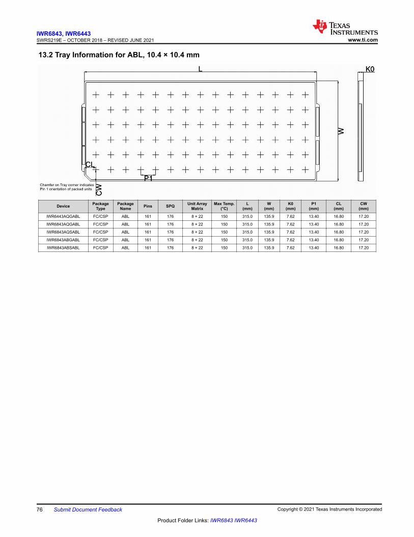
13.2 Tray Information for ABL, 10.4 × 10.4 mm
Device Package Type
Package Name Pins SPQ Unit Array
MatrixMax Temp.
(°C)L
(mm)W
(mm)K0
(mm)P1
(mm)CL
(mm)CW
(mm)
IWR6443AQGABL FC/CSP ABL 161 176 8 × 22 150 315.0 135.9 7.62 13.40 16.80 17.20
IWR6843AQGABL FC/CSP ABL 161 176 8 × 22 150 315.0 135.9 7.62 13.40 16.80 17.20
IWR6843AQSABL FC/CSP ABL 161 176 8 × 22 150 315.0 135.9 7.62 13.40 16.80 17.20
IWR6843ABGABL FC/CSP ABL 161 176 8 × 22 150 315.0 135.9 7.62 13.40 16.80 17.20
IWR6843ABSABL FC/CSP ABL 161 176 8 × 22 150 315.0 135.9 7.62 13.40 16.80 17.20
IWR6843, IWR6443SWRS219E – OCTOBER 2018 – REVISED JUNE 2021 www.ti.com
76 Submit Document Feedback Copyright © 2021 Texas Instruments Incorporated
Product Folder Links: IWR6843 IWR6443

PACKAGE OPTION ADDENDUM
www.ti.com 25-Feb-2021
Addendum-Page 1
PACKAGING INFORMATION
Orderable Device Status(1)
Package Type PackageDrawing
Pins PackageQty
Eco Plan(2)
Lead finish/Ball material
(6)
MSL Peak Temp(3)
Op Temp (°C) Device Marking(4/5)
Samples
IWR6443AQGABL ACTIVE FC/CSP ABL 161 176 RoHS & Green SNAGCU Level-3-260C-168 HR -40 to 105 IWR6443QG678A(678A ABL, 678 A ABL)
IWR6443AQGABLR ACTIVE FC/CSP ABL 161 1000 RoHS & Green SNAGCU Level-3-260C-168 HR -40 to 105 IWR6443QG678A(678A ABL, 678 A ABL)
IWR6843ABGABL ACTIVE FC/CSP ABL 161 176 RoHS & Green SNAGCU Level-3-260C-168 HR -40 to 105 IWR6843BG678A(678A ABL, 678 A ABL)
IWR6843ABGABLR ACTIVE FC/CSP ABL 161 1000 RoHS & Green SNAGCU Level-3-260C-168 HR -40 to 105 IWR6843BG678A(678A ABL, 678 A ABL)
IWR6843AQGABL ACTIVE FC/CSP ABL 161 176 RoHS & Green SNAGCU Level-3-260C-168 HR -40 to 105 IWR6843QG678A(678A ABL, 678 A ABL)
IWR6843AQGABLR ACTIVE FC/CSP ABL 161 1000 RoHS & Green SNAGCU Level-3-260C-168 HR -40 to 105 IWR6843QG678A(678A ABL, 678 A ABL)
IWR6843AQSABL ACTIVE FC/CSP ABL 161 176 RoHS & Green SNAGCU Level-3-260C-168 HR -40 to 105 IWR6843QS678A(678A ABL, 678 A ABL)
IWR6843AQSABLR ACTIVE FC/CSP ABL 161 1000 RoHS & Green SNAGCU Level-3-260C-168 HR -40 to 105 IWR6843QS

PACKAGE OPTION ADDENDUM
www.ti.com 25-Feb-2021
Addendum-Page 2
Orderable Device Status(1)
Package Type PackageDrawing
Pins PackageQty
Eco Plan(2)
Lead finish/Ball material
(6)
MSL Peak Temp(3)
Op Temp (°C) Device Marking(4/5)
Samples
678A(678A ABL, 678 A ABL)
(1) The marketing status values are defined as follows:ACTIVE: Product device recommended for new designs.LIFEBUY: TI has announced that the device will be discontinued, and a lifetime-buy period is in effect.NRND: Not recommended for new designs. Device is in production to support existing customers, but TI does not recommend using this part in a new design.PREVIEW: Device has been announced but is not in production. Samples may or may not be available.OBSOLETE: TI has discontinued the production of the device.
(2) RoHS: TI defines "RoHS" to mean semiconductor products that are compliant with the current EU RoHS requirements for all 10 RoHS substances, including the requirement that RoHS substancedo not exceed 0.1% by weight in homogeneous materials. Where designed to be soldered at high temperatures, "RoHS" products are suitable for use in specified lead-free processes. TI mayreference these types of products as "Pb-Free".RoHS Exempt: TI defines "RoHS Exempt" to mean products that contain lead but are compliant with EU RoHS pursuant to a specific EU RoHS exemption.Green: TI defines "Green" to mean the content of Chlorine (Cl) and Bromine (Br) based flame retardants meet JS709B low halogen requirements of <=1000ppm threshold. Antimony trioxide basedflame retardants must also meet the <=1000ppm threshold requirement.
(3) MSL, Peak Temp. - The Moisture Sensitivity Level rating according to the JEDEC industry standard classifications, and peak solder temperature.
(4) There may be additional marking, which relates to the logo, the lot trace code information, or the environmental category on the device.
(5) Multiple Device Markings will be inside parentheses. Only one Device Marking contained in parentheses and separated by a "~" will appear on a device. If a line is indented then it is a continuationof the previous line and the two combined represent the entire Device Marking for that device.
(6) Lead finish/Ball material - Orderable Devices may have multiple material finish options. Finish options are separated by a vertical ruled line. Lead finish/Ball material values may wrap to twolines if the finish value exceeds the maximum column width.
Important Information and Disclaimer:The information provided on this page represents TI's knowledge and belief as of the date that it is provided. TI bases its knowledge and belief on informationprovided by third parties, and makes no representation or warranty as to the accuracy of such information. Efforts are underway to better integrate information from third parties. TI has taken andcontinues to take reasonable steps to provide representative and accurate information but may not have conducted destructive testing or chemical analysis on incoming materials and chemicals.TI and TI suppliers consider certain information to be proprietary, and thus CAS numbers and other limited information may not be available for release.
In no event shall TI's liability arising out of such information exceed the total purchase price of the TI part(s) at issue in this document sold by TI to Customer on an annual basis.
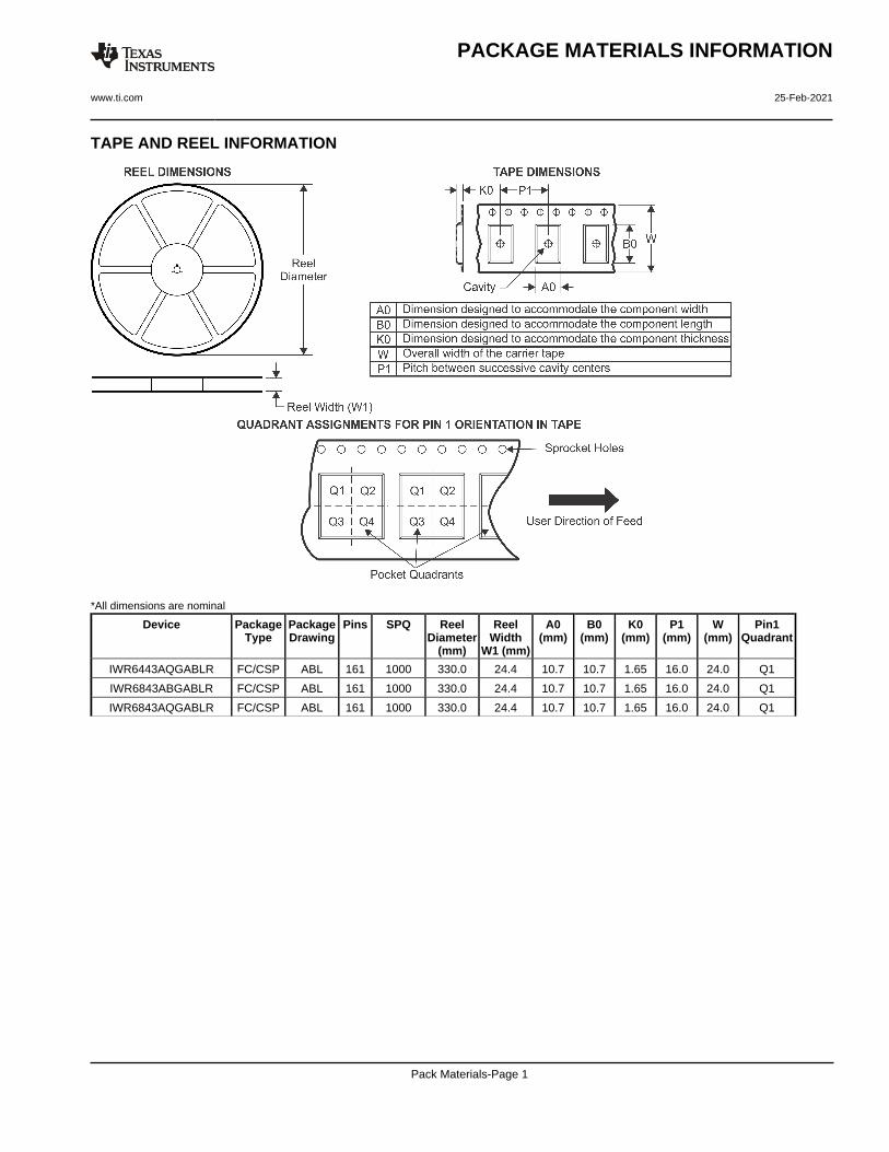
TAPE AND REEL INFORMATION
*All dimensions are nominal
Device PackageType
PackageDrawing
Pins SPQ ReelDiameter
(mm)
ReelWidth
W1 (mm)
A0(mm)
B0(mm)
K0(mm)
P1(mm)
W(mm)
Pin1Quadrant
IWR6443AQGABLR FC/CSP ABL 161 1000 330.0 24.4 10.7 10.7 1.65 16.0 24.0 Q1
IWR6843ABGABLR FC/CSP ABL 161 1000 330.0 24.4 10.7 10.7 1.65 16.0 24.0 Q1
IWR6843AQGABLR FC/CSP ABL 161 1000 330.0 24.4 10.7 10.7 1.65 16.0 24.0 Q1
PACKAGE MATERIALS INFORMATION
www.ti.com 25-Feb-2021
Pack Materials-Page 1
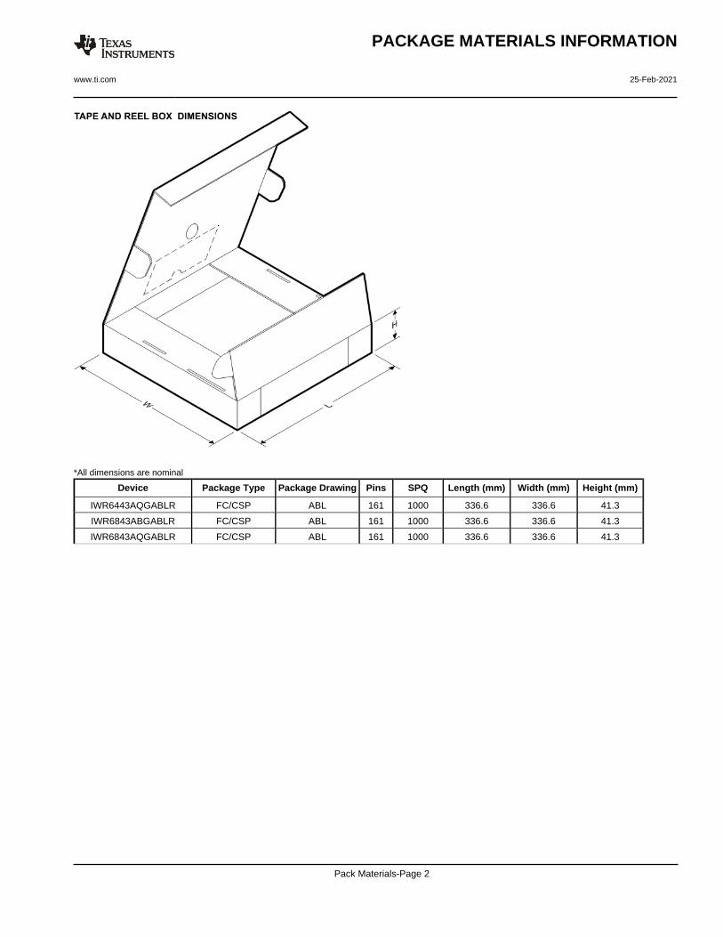
*All dimensions are nominal
Device Package Type Package Drawing Pins SPQ Length (mm) Width (mm) Height (mm)
IWR6443AQGABLR FC/CSP ABL 161 1000 336.6 336.6 41.3
IWR6843ABGABLR FC/CSP ABL 161 1000 336.6 336.6 41.3
IWR6843AQGABLR FC/CSP ABL 161 1000 336.6 336.6 41.3
PACKAGE MATERIALS INFORMATION
www.ti.com 25-Feb-2021
Pack Materials-Page 2

IMPORTANT NOTICE AND DISCLAIMERTI PROVIDES TECHNICAL AND RELIABILITY DATA (INCLUDING DATASHEETS), DESIGN RESOURCES (INCLUDING REFERENCEDESIGNS), APPLICATION OR OTHER DESIGN ADVICE, WEB TOOLS, SAFETY INFORMATION, AND OTHER RESOURCES “AS IS”AND WITH ALL FAULTS, AND DISCLAIMS ALL WARRANTIES, EXPRESS AND IMPLIED, INCLUDING WITHOUT LIMITATION ANYIMPLIED WARRANTIES OF MERCHANTABILITY, FITNESS FOR A PARTICULAR PURPOSE OR NON-INFRINGEMENT OF THIRDPARTY INTELLECTUAL PROPERTY RIGHTS.These resources are intended for skilled developers designing with TI products. You are solely responsible for (1) selecting the appropriateTI products for your application, (2) designing, validating and testing your application, and (3) ensuring your application meets applicablestandards, and any other safety, security, or other requirements. These resources are subject to change without notice. TI grants youpermission to use these resources only for development of an application that uses the TI products described in the resource. Otherreproduction and display of these resources is prohibited. No license is granted to any other TI intellectual property right or to any third partyintellectual property right. TI disclaims responsibility for, and you will fully indemnify TI and its representatives against, any claims, damages,costs, losses, and liabilities arising out of your use of these resources.TI’s products are provided subject to TI’s Terms of Sale (https:www.ti.com/legal/termsofsale.html) or other applicable terms available eitheron ti.com or provided in conjunction with such TI products. TI’s provision of these resources does not expand or otherwise alter TI’sapplicable warranties or warranty disclaimers for TI products.IMPORTANT NOTICE
Mailing Address: Texas Instruments, Post Office Box 655303, Dallas, Texas 75265Copyright © 2021, Texas Instruments Incorporated