isow784x high-performance, 5000-vrms reinforced quad
TRANSCRIPT

DC-DC Primary
DC-DCSecondary
VCC VISO
INx OUTx
VSI VSOIsolation Capacitor
Isolation Transformer
GNDI GNDO
Copyright © 2017, Texas Instruments Incorporated
VCC is the primary supply voltage referenced to GND1. VISO is the isolated supply voltage referenced to GND2.
VSI and VSO can be either VCC or VISO depending on the channel direction.
VSI is the input-side supply voltage referenced to GNDI and VSO is the output-side supply voltage referenced to GNDO.
Product
Folder
Order
Now
Technical
Documents
Tools &
Software
Support &Community
ReferenceDesign
An IMPORTANT NOTICE at the end of this data sheet addresses availability, warranty, changes, use in safety-critical applications,intellectual property matters and other important disclaimers. PRODUCTION DATA.
ISOW7840, ISOW7841ISOW7842, ISOW7843, ISOW7844
SLLSEY2E –MARCH 2017–REVISED NOVEMBER 2017
ISOW784x High-Performance, 5000-VRMS Reinforced Quad-Channel Digital Isolators WithIntegrated High-Efficiency, Low-Emissions DC-DC Converter
1
1 Features1• Integrated High-Efficiency DC-DC Converter With
On-Chip Transformer• 3-V to 5.5-V Wide Input Supply Range• Regulated 5-V or 3.3-V Output• Up to 0.65-W Output Power• 5 V to 5 V; 5 V to 3.3 V: Available Load Current ≥
130 mA• 3.3 V to 3.3 V: Available Load Current ≥ 75 mA• Soft-Start to Limit Inrush Current• Overload and Short-Circuit Protection• Thermal Shutdown• Default Output: High and Low Options• Signaling Rate Up to 100 Mbps• Low Propagation Delay: 13 ns Typ (5-V Supply)• High CMTI: ±100 kV/µs Minimum• Robust Electromagnetic Compatibility (EMC)
– System-Level ESD, EFT, and Surge Immunity– Low Emissions
• 16-pin Wide SOIC Package• Extended Temperature Range: –40°C to +125°C• Safety-Related Certifications:
– 7071-VPK Reinforced Isolation per DIN V VDEV 0884-11:2017-01
– 5000-VRMS Isolation for 1 Minute per UL 1577– CSA Certification per IEC 60950-1, IEC 62368-
1 and IEC 60601-1 End Equipment Standards– CQC Approval per GB4943.1-2011– TUV Certification According to EN 60950-1
and EN 61010-1
2 Applications• Industrial Automation• Motor Control• Grid Infrastructure• Medical Equipment• Test and Measurement
3 DescriptionThe ISOW784x is a family of high-performance,quad-channel reinforced digital isolators with anintegrated high-efficiency power converter. Theintegrated DC-DC converter provides up to 650 mWof isolated power at high efficiency and can beconfigured for various input and output voltageconfigurations. Therefore these devices eliminate theneed for a separate isolated power supply in space-constrained isolated designs.
The ISOW784x family of devices provide highelectromagnetic immunity and low emissions whileisolating CMOS or LVCMOS digital I/Os. The signal-isolation channel has a logic input and output bufferseparated by a silicon dioxide (SiO2) insulationbarrier, whereas, power isolation uses on-chiptransformers separated by thin film polymer asinsulating material. Various configurations of forwardand reverse channels are available. If the input signalis lost, the default output is high for the ISOW784xdevices and low for the devices with the F suffix (seethe Device Features).
Device Information(1)
PART NUMBER PACKAGE BODY SIZE (NOM)ISOW7840ISOW7841ISOW7842ISOW7843ISOW7844
SOIC (16) 10.30 mm × 7.50 mm
(1) For all available packages, see the orderable addendum atthe end of the data sheet.
Simplified Schematic

2
ISOW7840, ISOW7841ISOW7842, ISOW7843, ISOW7844SLLSEY2E –MARCH 2017–REVISED NOVEMBER 2017 www.ti.com
Product Folder Links: ISOW7840 ISOW7841 ISOW7842 ISOW7843 ISOW7844
Submit Documentation Feedback Copyright © 2017, Texas Instruments Incorporated
Table of Contents1 Features .................................................................. 12 Applications ........................................................... 13 Description ............................................................. 14 Revision History..................................................... 25 Description (continued)......................................... 46 Pin Configuration and Functions ......................... 47 Specifications......................................................... 6
7.1 Absolute Maximum Ratings ...................................... 67.2 ESD Ratings.............................................................. 67.3 Recommended Operating Conditions....................... 67.4 Thermal Information .................................................. 77.5 Power Ratings........................................................... 77.6 Insulation Specifications............................................ 87.7 Safety-Related Certifications..................................... 97.8 Safety Limiting Values .............................................. 97.9 Electrical Characteristics—5-V Input, 5-V Output ... 107.10 Supply Current Characteristics—5-V Input, 5-V
Output ...................................................................... 117.11 Electrical Characteristics—5-V Input, 3.3-V
Output ...................................................................... 147.12 Supply Current Characteristics—5-V Input, 3.3-V
Output ...................................................................... 157.13 Electrical Characteristics—3.3-V Input, 3.3-V
Output ...................................................................... 187.14 Supply Current Characteristics—3.3-V Input, 3.3-V
Output ...................................................................... 197.15 Switching Characteristics—5-V Input, 5-V Output 227.16 Switching Characteristics—5-V Input, 3.3-V
Output ...................................................................... 22
7.17 Switching Characteristics—3.3-V Input, 3.3-VOutput ...................................................................... 22
7.18 Insulation Characteristics Curves ......................... 237.19 Typical Characteristics .......................................... 24
8 Parameter Measurement Information ................ 299 Detailed Description ............................................ 30
9.1 Overview ................................................................. 309.2 Functional Block Diagram ....................................... 319.3 Feature Description................................................. 329.4 Device Functional Modes........................................ 33
10 Application and Implementation........................ 3510.1 Application Information.......................................... 3510.2 Typical Application ............................................... 35
11 Power Supply Recommendations ..................... 3712 Layout................................................................... 38
12.1 Layout Guidelines ................................................. 3812.2 Layout Example .................................................... 39
13 Device and Documentation Support ................. 4013.1 Device Support...................................................... 4013.2 Documentation Support ........................................ 4013.3 Related Links ........................................................ 4013.4 Receiving Notification of Documentation Updates 4013.5 Community Resources.......................................... 4013.6 Trademarks ........................................................... 4013.7 Electrostatic Discharge Caution............................ 4113.8 Glossary ................................................................ 41
14 Mechanical, Packaging, and OrderableInformation ........................................................... 41
4 Revision HistoryNOTE: Page numbers for previous revisions may differ from page numbers in the current version.
Changes from Revision D (November 2017) to Revision E Page
• Changed the ISOW7843 device from Preview to Production Data ........................................................................................ 1• Added the ISOW7843 current parameters to each Supply Current Characteristics table .................................................. 12• Added the supply current versus data rate graphs for the ISOW7843 in the Typical Characteristics section..................... 25
Changes from Revision C (October 2017) to Revision D Page
• Changed the ISOW7840 device from Preview to Production Data ........................................................................................ 1• Added the ISOW7840 current parameters to each Supply Current Characteristics table .................................................. 11• Changed IISO to ILOAD and the value of wave clock input from 0.5, 5, and 50 MHz to 1, 10, and 100 Mbps in the test
conditions for the ISOW7841 current parameters in each Supply Current Characteristics table ....................................... 11• Deleted no external ILOAD test condition for the current available to isolated supply parameter for the ISOW7842 and
ISOW7844 devices in each Supply Current Characteristics table ...................................................................................... 12• Changed the labels of the curves in the Thermal Derating Curve for Safety Limiting Current per VDE ............................. 23• Added the supply current versus data rate graphs for the ISOW7840 in the Typical Characteristics section..................... 24• Changed the ground symbols for the input schematic for devices with F suffix and the SEL pin in the Device I/O
Schematics figure ................................................................................................................................................................. 34

3
ISOW7840, ISOW7841ISOW7842, ISOW7843, ISOW7844
www.ti.com SLLSEY2E –MARCH 2017–REVISED NOVEMBER 2017
Product Folder Links: ISOW7840 ISOW7841 ISOW7842 ISOW7843 ISOW7844
Submit Documentation FeedbackCopyright © 2017, Texas Instruments Incorporated
Changes from Revision B (June 2017) to Revision C Page
• Changed the Safety-Related Certifications Features list........................................................................................................ 1• Changed header row From: DIN V VDE 0884-10 (VDE V 0884-10): 2016-12 To: DIN V VDE 0884-11:2017-01 in the
Insulation Specifications ......................................................................................................................................................... 8• Changed VIOSM test conditions in Insulation Specifications .................................................................................................... 8• Changed VISO(UL) test conditions in Insulation Specifications ................................................................................................. 8• Changed the Safety-Related Certifications table.................................................................................................................... 9• Changed Note 1 of the Safety Limiting Values table.............................................................................................................. 9• Added the ISOW7842 current parameters to each Supply Current table ........................................................................... 12• Added the supply current versus data rate graphs for the ISOW7842 in the Typical Characteristics section..................... 25
Changes from Revision A (March 2017) to Revision B Page
• Added the ISOW7844 current parameters to each Supply Current table ........................................................................... 13
Changes from Original (March 2017) to Revision A Page
• Changed the maximum propagation delay time and the typical and maximum values for pulse width distortion in allSwitching Characteristics tables........................................................................................................................................... 22
• Changed the maximum limit for output signal rise and fall times from 3 to 4 ns in the Switching Characteristics—5-VInput, 3.3-V Output table ...................................................................................................................................................... 22

VCC
GND1
INA
OUTB
OUTC
OUTD
NC
GND1
1
2
3
4
5
6
7
8
VISO
GND2
16
15
14
13
12
11
10
9
OUTA
INB
INC
IND
SEL
GND2
ISO
LAT
ION
VCC
GND1
INA
INB
OUTC
OUTD
NC
GND1
1
2
3
4
5
6
7
8
VISO
GND2
16
15
14
13
12
11
10
9
OUTA
OUTB
INC
IND
SEL
GND2
ISO
LAT
ION
VCC
GND1
INA
INB
INC
OUTD
NC
GND1
1
2
3
4
5
6
7
8
VISO
GND2
16
15
14
13
12
11
10
9
OUTA
OUTB
OUTC
IND
SEL
GND2
ISO
LAT
ION
VCC
GND1
INA
INB
INC
IND
NC
GND1
1
2
3
4
5
6
7
8
VISO
GND2
16
15
14
13
12
11
10
9
OUTA
OUTB
OUTC
OUTD
SEL
GND2
ISO
LAT
ION
4
ISOW7840, ISOW7841ISOW7842, ISOW7843, ISOW7844SLLSEY2E –MARCH 2017–REVISED NOVEMBER 2017 www.ti.com
Product Folder Links: ISOW7840 ISOW7841 ISOW7842 ISOW7843 ISOW7844
Submit Documentation Feedback Copyright © 2017, Texas Instruments Incorporated
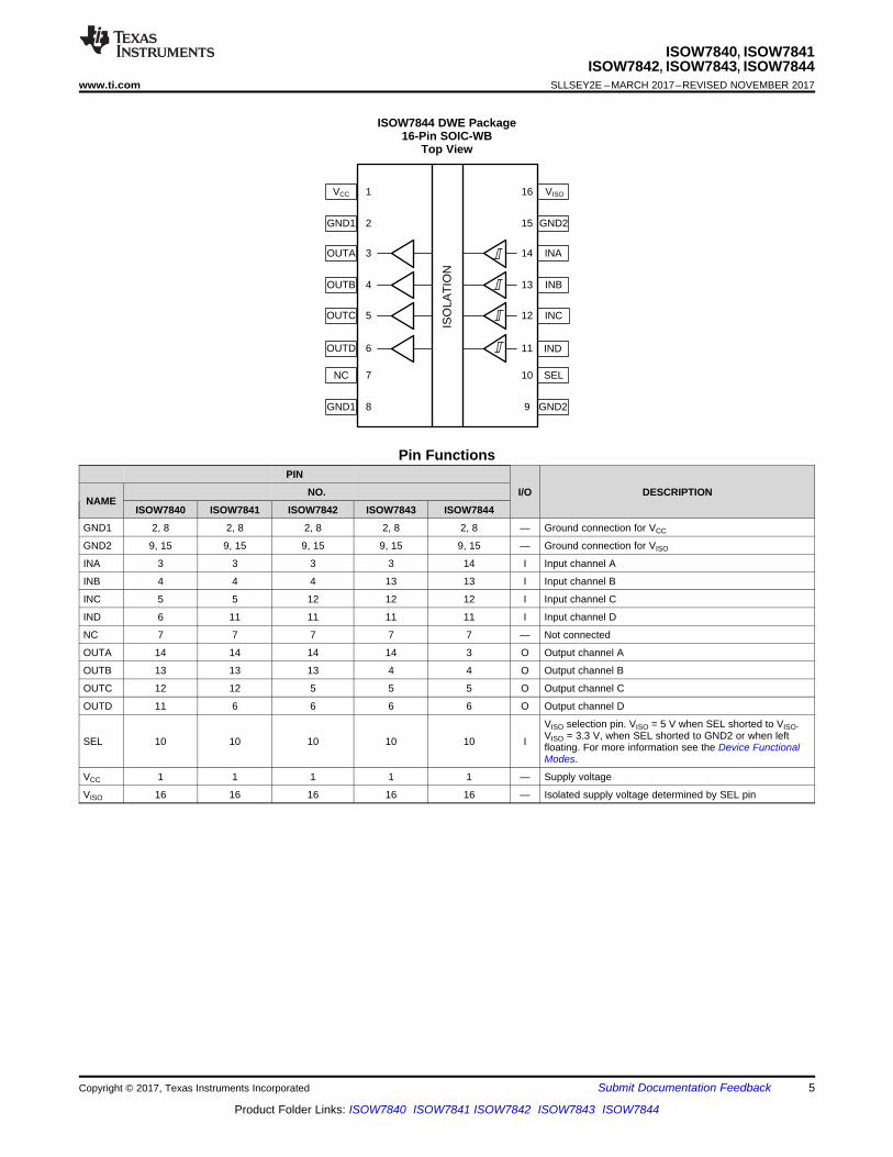
5 Description (continued)These devices help prevent noise currents on a data bus or other circuits from entering the local ground andinterfering with or damaging sensitive circuitry. Through innovative chip design and layout techniques,electromagnetic compatibility of the ISOW784x family of devices has been significantly enhanced to easesystem-level ESD, EFT, surge and emissions compliance. The high-efficiency of the power converter allowsoperation at a higher ambient temperature. The ISOW784x family of devices is available in a 16-pin SOIC wide-body (SOIC-WB) DWE package.
6 Pin Configuration and Functions
ISOW7840 DWE Package16-Pin SOIC-WB
Top View
ISOW7841 DWE Package16-Pin SOIC-WB
Top View
ISOW7842 DWE Package16-Pin SOIC-WB
Top ViewISOW7843 DWE Package
16-Pin SOIC-WBTop View
VCC
GND1
OUTA
OUTB
OUTC
OUTD
NC
GND1
1
2
3
4
5
6
7
8
VISO
GND2
16
15
14
13
12
11
10
9
INA
INB
INC
IND
SEL
GND2
ISO
LAT
ION
5
ISOW7840, ISOW7841ISOW7842, ISOW7843, ISOW7844
www.ti.com SLLSEY2E –MARCH 2017–REVISED NOVEMBER 2017
Product Folder Links: ISOW7840 ISOW7841 ISOW7842 ISOW7843 ISOW7844
Submit Documentation FeedbackCopyright © 2017, Texas Instruments Incorporated
ISOW7844 DWE Package16-Pin SOIC-WB
Top View
Pin FunctionsPIN
I/O DESCRIPTIONNAME
NO.
ISOW7840 ISOW7841 ISOW7842 ISOW7843 ISOW7844
GND1 2, 8 2, 8 2, 8 2, 8 2, 8 — Ground connection for VCC
GND2 9, 15 9, 15 9, 15 9, 15 9, 15 — Ground connection for VISO
INA 3 3 3 3 14 I Input channel A
INB 4 4 4 13 13 I Input channel B
INC 5 5 12 12 12 I Input channel C
IND 6 11 11 11 11 I Input channel D
NC 7 7 7 7 7 — Not connected
OUTA 14 14 14 14 3 O Output channel A
OUTB 13 13 13 4 4 O Output channel B
OUTC 12 12 5 5 5 O Output channel C
OUTD 11 6 6 6 6 O Output channel D
SEL 10 10 10 10 10 I
VISO selection pin. VISO = 5 V when SEL shorted to VISO.VISO = 3.3 V, when SEL shorted to GND2 or when leftfloating. For more information see the Device FunctionalModes.
VCC 1 1 1 1 1 — Supply voltage
VISO 16 16 16 16 16 — Isolated supply voltage determined by SEL pin

6
ISOW7840, ISOW7841ISOW7842, ISOW7843, ISOW7844SLLSEY2E –MARCH 2017–REVISED NOVEMBER 2017 www.ti.com
Product Folder Links: ISOW7840 ISOW7841 ISOW7842 ISOW7843 ISOW7844
Submit Documentation Feedback Copyright © 2017, Texas Instruments Incorporated
(1) Stresses beyond those listed under Absolute Maximum Ratings may cause permanent damage to the device. These are stress ratingsonly, which do not imply functional operation of the device at these or any other conditions beyond those indicated under RecommendedOperating Conditions. Exposure to absolute-maximum-rated conditions for extended periods may affect device reliability.
(2) All voltage values except differential I/O bus voltages are with respect to the local ground pin (GND1 or GND2) and are peak voltagevalues.
(3) This value depends on whether the pin is located on the VCC or VISO side. The maximum voltage at the I/O pins should not exceed 6 V.
7 Specifications
7.1 Absolute Maximum RatingsSee (1) (2)
MIN MAX UNITVCC Supply voltage –0.5 6 VVISO Isolated supply voltage –0.5 6 V
VIO Voltage at INx, OUTx, SEL pins –0.5 VCC + 0.5,VISO + 0.5 (3) V
IO Maximum output current through data channels –15 15 mATJ Junction temperature 150 °CTstg Storage temperature –65 150 °C
(1) JEDEC document JEP155 states that 500-V HBM allows safe manufacturing with a standard ESD control process(2) JEDEC document JEP157 states that 250-V CDM allows safe manufacturing with a standard ESD control process.
7.2 ESD RatingsVALUE UNIT
V(ESD)Electrostaticdischarge
Human-body model (HBM), per ANSI/ESDA/JEDEC JS-001 (1) ±2000V
Charged-device model (CDM), per JEDEC specification JESD22-C101 (2) ±1000
(1) VSI is the input side supply, VSO is the output side supply(2) This current is for data output channel.
7.3 Recommended Operating ConditionsMIN NOM MAX UNIT
VCC Supply voltage 3 5.5 V
IOH High level output current (2) VSO(1) = 5 V –4
mAVSO = 3.3 V –2
IOL Low level output current (2) VSO = 5 V 4mA
VSO = 3.3 V 2VIH High-level input voltage 0.7 × VSI VSI VVIL Low-level input voltage 0 0.3 × VSI VDR Data rate 100 MbpsTJ Junction temperature –40 150 °CTA Ambient temperature –40 125 °C

7
ISOW7840, ISOW7841ISOW7842, ISOW7843, ISOW7844
www.ti.com SLLSEY2E –MARCH 2017–REVISED NOVEMBER 2017
Product Folder Links: ISOW7840 ISOW7841 ISOW7842 ISOW7843 ISOW7844
Submit Documentation FeedbackCopyright © 2017, Texas Instruments Incorporated
(1) For more information about traditional and new thermal metrics, see the Semiconductor and IC Package Thermal Metrics applicationreport.
7.4 Thermal Information
THERMAL METRIC (1)ISOW784x
UNITDWE (SOIC)16 PINS
RθJA Junction-to-ambient thermal resistance 56.8 °C/WRθJC(top) Junction-to-case (top) thermal resistance 15.6 °C/WRθJB Junction-to-board thermal resistance 28.5 °C/WΨJT Junction-to-top characterization parameter 2.4 °C/WΨJB Junction-to-board characterization parameter 28.5 °C/WRθJC(bot) Junction-to-case (bottom) thermal resistance — °C/W
7.5 Power RatingsVCC = 5.5 V, IISO = 110 mA, TJ = 150°C, TA ≤ 80°C, CL = 15 pF, input a 50-MHz 50% duty-cycle square wave
PARAMETER TEST CONDITIONS MIN TYP MAX UNITPD Maximum power dissipation (both sides) 1.02 WPD1 Maximum power dissipation (side-1) 0.51 WPD2 Maximum power dissipation (side-2) 0.51 W

8
ISOW7840, ISOW7841ISOW7842, ISOW7843, ISOW7844SLLSEY2E –MARCH 2017–REVISED NOVEMBER 2017 www.ti.com
Product Folder Links: ISOW7840 ISOW7841 ISOW7842 ISOW7843 ISOW7844
Submit Documentation Feedback Copyright © 2017, Texas Instruments Incorporated
(1) Creepage and clearance requirements should be applied according to the specific equipment isolation standards of an application. Careshould be taken to maintain the creepage and clearance distance of a board design to ensure that the mounting pads of the isolator onthe printed-circuit board do not reduce this distance. Creepage and clearance on a printed-circuit board become equal in certain cases.Techniques such as inserting grooves, ribs, or both on a printed circuit board are used to help increase these specifications.
(2) This coupler is suitable for safe electrical insulation only within the safety ratings. Compliance with the safety ratings shall be ensured bymeans of suitable protective circuits.
(3) Testing is carried out in air or oil to determine the intrinsic surge immunity of the isolation barrier.(4) Apparent charge is electrical discharge caused by a partial discharge (pd).(5) All pins on each side of the barrier tied together creating a two-terminal device.
7.6 Insulation SpecificationsPARAMETER TEST CONDITIONS VALUE UNIT
GENERALCLR External clearance (1) Shortest terminal-to-terminal distance through air >8 mm
CPG External creepage (1) Shortest terminal-to-terminal distance across thepackage surface >8 mm
DTI Distance through the insulation
Minimum internal gap (internal clearance – capacitivesignal isolation) > 21
µmMinimum internal gap (internal clearance –transformer power isolation) >120
CTI Comparative tracking index DIN EN 60112 (VDE 0303-11); IEC 60112 > 600 VMaterial group According to IEC 60664-1 I
Overvoltage category per IEC 60664-1Rated mains voltage ≤ 300 VRMS I-IVRated mains voltage ≤ 600 VRMS I-IVRated mains voltage ≤ 1000 VRMS I-III
DIN V VDE 0884-11:2017-01 (2)
VIORMMaximum repetitive peak isolationvoltage AC voltage (bipolar) 1414 VPK
VIOWM Maximum working isolation voltageAC voltage; Time dependent dielectric breakdown(TDDB) Test 1000 VRMS
DC voltage 1414 VDC
VIOTM Maximum transient isolation voltage VTEST = VIOTM; t = 60 s (qualification);VTEST = 1.2 × VIOTM; t = 1 s (100% production) 7071 VPK
VIOSM Maximum surge isolation voltage (3) Test method per IEC 62368-1, 1.2/50 µs waveform,VTEST = 1.6 × VIOSM = 10000 VPK(qualification) 6250 VPK
qpd Apparent charge (4)
Method a, after input/output safety test subgroup 2/3,Vini = VIOTM, tini = 60 s;Vpd(m) = 1.2 × VIORM, tm = 10 s
≤ 5
pCMethod a, after environmental tests subgroup 1,Vini = VIOTM, tini = 60 s; Vpd(m) = 1.6 × VIORM, tm = 10 s ≤ 5
Method b1, at routine test (100% production) andpreconditioning (type test),Vini = 1.2 × VIOTM, tini = 1 s;Vpd(m) = 1.875 × VIORM, tm = 1 s
≤ 5
CIO Barrier capacitance, input to output (5) VIO = 0.4 × sin (2πft), f = 1 MHz ~3.5 pF
RIO Insulation resistance (5)
VIO = 500 V, TA = 25°C > 1012
ΩVIO = 500 V, 100°C ≤ TA ≤ 125°C > 1011
VIO = 500 V, TS = 150°C > 109
Pollution degree 2Climatic category 40/125/21
UL 1577
VISO(UL) Withstand isolation voltageVTEST = VISO(UL)= 5000 VRMS, t = 60 s (qualification),VTEST = 1.2 × VISO(UL) = 6000 VRMS, t = 1 s (100%production)
5000 VRMS

9
ISOW7840, ISOW7841ISOW7842, ISOW7843, ISOW7844
www.ti.com SLLSEY2E –MARCH 2017–REVISED NOVEMBER 2017
Product Folder Links: ISOW7840 ISOW7841 ISOW7842 ISOW7843 ISOW7844
Submit Documentation FeedbackCopyright © 2017, Texas Instruments Incorporated
7.7 Safety-Related CertificationsVDE CSA UL CQC TUV
Certified according to DINV VDE V 0884-11:2017-01
Certified according to IEC60950-1, IEC 62368-1, and IEC60601-1
Recognized under UL1577 ComponentRecognition Program
Certified according toGB 4943.1-2011
Certified according to EN61010-1:2010 and EN60950- 1:2006/A2:2013
Reinforced insulation;Maximum transientisolation voltage, 7071VPK;Maximum repetitive peakisolation voltage, 1414VPK;Maximum surge isolationvoltage, 6250 VPK
Reinforced insulation per CSA60950-1-07+A1+A2, IEC60950-1 2nd Ed.+A1+A2, CSA62368-1-14 and IEC 62368-12nd Ed., 800 VRMS maximumworking voltage (pollutiondegree 2, material group I);2 MOPP (Means of PatientProtection) per CSA 60601-1:14and IEC 60601-1 Ed. 3+A1, 250VRMS maximum workingvoltage;Temperature rating is 90°C forreinforced insulation and 125°Cfor basic insulation; seecertificate for details.
Single protection, 5000VRMS
Reinforced Insulation,Altitude ≤ 5000 m,Tropical Climate, 700VRMS maximumworking voltage;
5000 VRMS Reinforcedinsulation per EN 61010-1:2010 up to workingvoltage of 600 VRMS;5000 VRMS Reinforcedinsulation per EN 60950-1:2006/A2:2013 up toworking voltage of 800VRMS
Certificate number:40040142
Master contract number:220991
File number: E181974 Certificate number:CQC15001121716
Client ID number: 77311
(1) The maximum safety temperature, TS, has the same value as the maximum junction temperature, TJ, specified for the device. The ISand PS parameters represent the safety current and safety power respectively. The maximum limits of IS and PS should not beexceeded. These limits vary with the ambient temperature, TA.The junction-to-air thermal resistance, RθJA, in the Thermal Information table is that of a device installed on a high-K test board forleaded surface-mount packages. Use the following equations to calculate the value for each parameter:TJ = TA + RθJA × P, where P is the power dissipated in the device.TJ(max) = TS = TA + RθJA × PS, where TJ(max) is the maximum allowed junction temperature.PS = IS × VI, where VI is the maximum input voltage.
7.8 Safety Limiting ValuesSafety limiting intends to minimize potential damage to the isolation barrier upon failure of input or output circuitry.
PARAMETER TEST CONDITIONS MIN TYP MAX UNIT
IS Safety input, output, or supply current (1)
RθJA = 56.8°C/W, VI = 5.5 V, TJ = 150°C,TA = 25°C, see Figure 1 400
mARθJA = 56.8°C/W, VI = 3.6 V, TJ = 150°C,TA = 25°C, see Figure 1 611
PS Safety input, output, or total power (1) RθJA = 56.8°C/W, TJ = 150°C, TA = 25°C,see Figure 2 2200 mW
TS Maximum safety temperature (1) 150 °C
10
ISOW7840, ISOW7841ISOW7842, ISOW7843, ISOW7844SLLSEY2E –MARCH 2017–REVISED NOVEMBER 2017 www.ti.com
Product Folder Links: ISOW7840 ISOW7841 ISOW7842 ISOW7843 ISOW7844
Submit Documentation Feedback Copyright © 2017, Texas Instruments Incorporated
(1) VSI = input side supply; VSO = output side supply
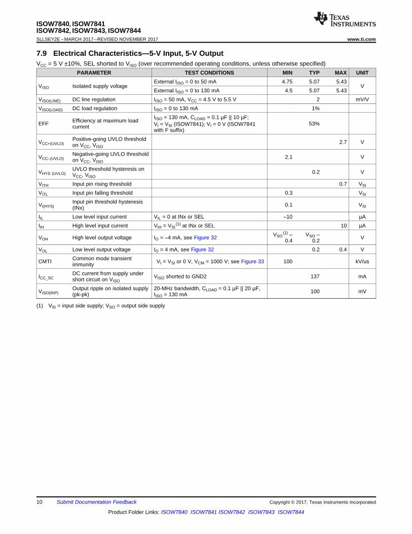
7.9 Electrical Characteristics—5-V Input, 5-V OutputVCC = 5 V ±10%, SEL shorted to VISO (over recommended operating conditions, unless otherwise specified)
PARAMETER TEST CONDITIONS MIN TYP MAX UNIT
VISO Isolated supply voltageExternal IISO = 0 to 50 mA 4.75 5.07 5.43
VExternal IISO = 0 to 130 mA 4.5 5.07 5.43
VISO(LINE) DC line regulation IISO = 50 mA, VCC = 4.5 V to 5.5 V 2 mV/VVISO(LOAD) DC load regulation IISO = 0 to 130 mA 1%
EFF Efficiency at maximum loadcurrent
IISO = 130 mA, CLOAD = 0.1 µF || 10 µF;VI = VSI (ISOW7841); VI = 0 V (ISOW7841with F suffix)
53%
VCC+(UVLO)Positive-going UVLO thresholdon VCC, VISO
2.7 V
VCC–(UVLO)Negative-going UVLO thresholdon VCC, VISO
2.1 V
VHYS (UVLO)UVLO threshold hysteresis onVCC, VISO
0.2 V
VITH Input pin rising threshold 0.7 VSI
VITL Input pin falling threshold 0.3 VSI
VI(HYS)Input pin threshold hysteresis(INx) 0.1 VSI
IIL Low level input current VIL = 0 at INx or SEL –10 µAIIH High level input current VIH = VSI
(1) at INx or SEL 10 µA
VOH High level output voltage IO = –4 mA, see Figure 32 VSO(1) –0.4
VSO –0.2 V
VOL Low level output voltage IO = 4 mA, see Figure 32 0.2 0.4 V
CMTI Common mode transientimmunity VI = VSI or 0 V, VCM = 1000 V; see Figure 33 100 kV/us
ICC_SCDC current from supply undershort circuit on VISO
VISO shorted to GND2 137 mA
VISO(RIP)Output ripple on isolated supply(pk-pk)
20-MHz bandwidth, CLOAD = 0.1 µF || 20 µF,IISO = 130 mA 100 mV
11
ISOW7840, ISOW7841ISOW7842, ISOW7843, ISOW7844
www.ti.com SLLSEY2E –MARCH 2017–REVISED NOVEMBER 2017
Product Folder Links: ISOW7840 ISOW7841 ISOW7842 ISOW7843 ISOW7844
Submit Documentation FeedbackCopyright © 2017, Texas Instruments Incorporated
(1) VSI = input side supply; VSO = output side supply(2) Current available to load should be derated by 2 mA/°C for TA > 80°C.
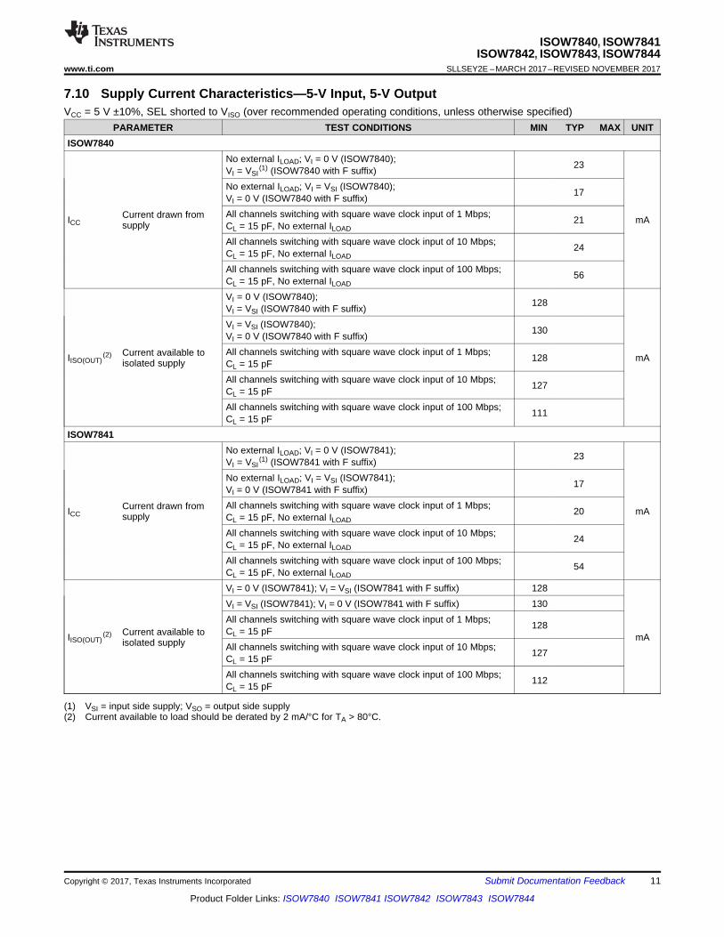
7.10 Supply Current Characteristics—5-V Input, 5-V OutputVCC = 5 V ±10%, SEL shorted to VISO (over recommended operating conditions, unless otherwise specified)
PARAMETER TEST CONDITIONS MIN TYP MAX UNITISOW7840
ICCCurrent drawn fromsupply
No external ILOAD; VI = 0 V (ISOW7840);VI = VSI
(1) (ISOW7840 with F suffix) 23
mA
No external ILOAD; VI = VSI (ISOW7840);VI = 0 V (ISOW7840 with F suffix) 17
All channels switching with square wave clock input of 1 Mbps;CL = 15 pF, No external ILOAD
21
All channels switching with square wave clock input of 10 Mbps;CL = 15 pF, No external ILOAD
24
All channels switching with square wave clock input of 100 Mbps;CL = 15 pF, No external ILOAD
56
IISO(OUT)(2) Current available to
isolated supply
VI = 0 V (ISOW7840);VI = VSI (ISOW7840 with F suffix) 128
mA
VI = VSI (ISOW7840);VI = 0 V (ISOW7840 with F suffix) 130
All channels switching with square wave clock input of 1 Mbps;CL = 15 pF 128
All channels switching with square wave clock input of 10 Mbps;CL = 15 pF 127
All channels switching with square wave clock input of 100 Mbps;CL = 15 pF 111
ISOW7841
ICCCurrent drawn fromsupply
No external ILOAD; VI = 0 V (ISOW7841);VI = VSI
(1) (ISOW7841 with F suffix) 23
mA
No external ILOAD; VI = VSI (ISOW7841);VI = 0 V (ISOW7841 with F suffix) 17
All channels switching with square wave clock input of 1 Mbps;CL = 15 pF, No external ILOAD
20
All channels switching with square wave clock input of 10 Mbps;CL = 15 pF, No external ILOAD
24
All channels switching with square wave clock input of 100 Mbps;CL = 15 pF, No external ILOAD
54
IISO(OUT)(2) Current available to
isolated supply
VI = 0 V (ISOW7841); VI = VSI (ISOW7841 with F suffix) 128
mA
VI = VSI (ISOW7841); VI = 0 V (ISOW7841 with F suffix) 130All channels switching with square wave clock input of 1 Mbps;CL = 15 pF 128
All channels switching with square wave clock input of 10 Mbps;CL = 15 pF 127
All channels switching with square wave clock input of 100 Mbps;CL = 15 pF 112

12
ISOW7840, ISOW7841ISOW7842, ISOW7843, ISOW7844SLLSEY2E –MARCH 2017–REVISED NOVEMBER 2017 www.ti.com
Product Folder Links: ISOW7840 ISOW7841 ISOW7842 ISOW7843 ISOW7844
Submit Documentation Feedback Copyright © 2017, Texas Instruments Incorporated
Supply Current Characteristics—5-V Input, 5-V Output (continued)VCC = 5 V ±10%, SEL shorted to VISO (over recommended operating conditions, unless otherwise specified)
PARAMETER TEST CONDITIONS MIN TYP MAX UNITISOW7842
ICCCurrent drawn fromsupply
No external ILOAD; VI = 0 V (ISOW7842);VI = VSI
(1) (ISOW7842 with F suffix) 24
mA
No external ILOAD; VI = VSI (ISOW7842);VI = 0 V (ISOW7842 with F suffix) 18
All channels switching with square wave clock input of 1 Mbps;CL = 15 pF, No external ILOAD
21
All channels switching with square wave clock input of 10 Mbps;CL = 15 pF, No external ILOAD
24
All channels switching with square wave clock input of 100 Mbps;CL = 15 pF, No external ILOAD
51
IISO(OUT)(2) Current available to
isolated supply
VI = 0 V (ISOW7842);VI = VSI (ISOW7842 with F suffix) 126
mA
VI = VSI (ISOW7842);VI = 0 V (ISOW7842 with F suffix) 130
All channels switching with square wave clock input of 1 Mbps;CL = 15 pF 128
All channels switching with square wave clock input of 10 Mbps;CL = 15 pF 127
All channels switching with square wave clock input of 100 Mbps;CL = 15 pF 116
ISOW7843
ICCCurrent drawn fromsupply
No external ILOAD; VI = 0 V (ISOW7843);VI = VSI
(1) (ISOW7843 with F suffix) 25
mA
No external ILOAD; VI = VSI (ISOW7843);VI = 0 V (ISOW7843 with F suffix) 17
All channels switching with square wave clock input of 1 Mbps;CL = 15 pF, No external ILOAD
21
All channels switching with square wave clock input of 10 Mbps;CL = 15 pF, No external ILOAD
24
All channels switching with square wave clock input of 100 Mbps;CL = 15 pF, No external ILOAD
48
IISO(OUT)(2) Current available to
isolated supply
VI = 0 V (ISOW7843);VI = VSI (ISOW7843 with F suffix) 125
mA
VI = VSI (ISOW7843);VI = 0 V (ISOW7843 with F suffix) 130
All channels switching with square wave clock input of 1 Mbps;CL = 15 pF 127
All channels switching with square wave clock input of 10 Mbps;CL = 15 pF 126
All channels switching with square wave clock input of 100 Mbps;CL = 15 pF 120

13
ISOW7840, ISOW7841ISOW7842, ISOW7843, ISOW7844
www.ti.com SLLSEY2E –MARCH 2017–REVISED NOVEMBER 2017
Product Folder Links: ISOW7840 ISOW7841 ISOW7842 ISOW7843 ISOW7844
Submit Documentation FeedbackCopyright © 2017, Texas Instruments Incorporated
Supply Current Characteristics—5-V Input, 5-V Output (continued)VCC = 5 V ±10%, SEL shorted to VISO (over recommended operating conditions, unless otherwise specified)
PARAMETER TEST CONDITIONS MIN TYP MAX UNITISOW7844
ICCCurrent drawn fromsupply
No external ILOAD; VI = 0 V (ISOW7844);VI = VSI
(1) (ISOW7844 with F suffix) 26
mA
No external ILOAD; VI = VSI (ISOW7844);VI = 0 V (ISOW7844 with F suffix) 17
All channels switching with square wave clock input of 1 Mbps;CL = 15 pF, No external ILOAD
22
All channels switching with square wave clock input of 10 Mbps;CL = 15 pF, No external ILOAD
24
All channels switching with square wave clock input of 100 Mbps;CL = 15 pF, No external ILOAD
46
IISO(OUT)(2) Current available to
isolated supply
VI = 0 V (ISOW7844);VI = VSI (ISOW7844 with F suffix) 123
mA
VI = VSI (ISOW7844);VI = 0 V (ISOW7844 with F suffix) 130
All channels switching with square wave clock input of 1 Mbps;CL = 15 pF 126
All channels switching with square wave clock input of 10 Mbps;CL = 15 pF 126
All channels switching with square wave clock input of 100 Mbps;CL = 15 pF 126

14
ISOW7840, ISOW7841ISOW7842, ISOW7843, ISOW7844SLLSEY2E –MARCH 2017–REVISED NOVEMBER 2017 www.ti.com
Product Folder Links: ISOW7840 ISOW7841 ISOW7842 ISOW7843 ISOW7844
Submit Documentation Feedback Copyright © 2017, Texas Instruments Incorporated
(1) VSI = input side supply; VSO = output side supply
7.11 Electrical Characteristics—5-V Input, 3.3-V OutputVCC = 5 V ±10%, SEL shorted to GND2 (over recommended operating conditions, unless otherwise specified)
PARAMETER TEST CONDITIONS MIN TYP MAX UNIT
VISO Isolated supply voltageExternal IISO = 0 to 50 mA 3.13 3.34 3.56
VExternal IISO = 0 to 130 mA 3 3.34 3.56
VISO(LINE) DC line regulation IISO = 50 mA, VCC = 4.5 V to 5.5 V 2 mV/VVISO(LOAD) DC load regulation IISO = 10 to 130 mA 1%
EFF Efficiency at maximum loadcurrent
IISO = 130 mA, CLOAD = 0.1 µF || 10 µF;VI = VSI (ISOW7841); VI = 0 V (ISOW7841with F suffix)
48%
VCC+(UVLO)Positive-going UVLO thresholdon VCC, VISO
2.7 V
VCC–(UVLO)Negative-going UVLO thresholdon VCC, VISO
2.1 V
VHYS (UVLO)UVLO threshold hysteresis onVCC, VISO
0.2 V
VITH Input pin rising threshold 0.7 VSI
VITL Input pin falling threshold 0.3 VSI
VI(HYS)Input pin threshold hysteresis(INx) 0.1 VSI
IIL Low level input current VIL = 0 at INx or SEL –10 µAIIH High level input current VIH = VSI
(1) at INx or SEL 10 µA
VOH High level output voltage IO = –2 mA, see Figure 32 VSO(1) –0.3
VSO –0.1 V
VOL Low level output voltage IO = 2 mA, see Figure 32 0.1 0.3 V
CMTI Common mode transientimmunity
VI = VSI or 0 V, VCM = 1000 V; seeFigure 33 100 kV/us
ICC_SCDC current from supply undershort circuit on VISO
VISO shorted to GND2 137 mA
VISO(RIP)Output ripple on isolated supply(pk-pk)
20-MHz bandwidth, CLOAD = 0.1 µF || 20 µF,IISO = 130 mA 100 mV

15
ISOW7840, ISOW7841ISOW7842, ISOW7843, ISOW7844
www.ti.com SLLSEY2E –MARCH 2017–REVISED NOVEMBER 2017
Product Folder Links: ISOW7840 ISOW7841 ISOW7842 ISOW7843 ISOW7844
Submit Documentation FeedbackCopyright © 2017, Texas Instruments Incorporated
(1) VSI = input side supply; VSO = output side supply(2) Current available to load should be derated by 2 mA/°C for TA > 105°C.
7.12 Supply Current Characteristics—5-V Input, 3.3-V OutputVCC = 5 V ±10%, SEL shorted to GND2 (over recommended operating conditions, unless otherwise specified)
PARAMETER TEST CONDITIONS MIN TYP MAX UNITISOW7840
ICCCurrent drawn fromsupply
No external ILOAD; VI = 0 V (ISOW7840);VI = VSI
(1) (ISOW7840 with F suffix) 20
mA
No external ILOAD; VI = VSI (ISOW7840);VI = 0 V (ISOW7840 with F suffix) 15
All channels switching with square wave clock input of 1 Mbps;CL = 15 pF, No external ILOAD
17
All channels switching with square wave clock input of 10 Mbps;CL = 15 pF, No external ILOAD
19
All channels switching with square wave clock input of 100 Mbps;CL = 15 pF, No external ILOAD
39
IISO(OUT)(2) Current available to
isolated supply
VI = 0 V (ISOW7840);VI = VSI (ISOW7840 with F suffix) 128
mA
VI = VSI (ISOW7840);VI = 0 V (ISOW7840 with F suffix) 130
All channels switching with square wave clock input of 1 Mbps;CL = 15 pF 129
All channels switching with square wave clock input of 10 Mbps;CL = 15 pF 128
All channels switching with square wave clock input of 100 Mbps;CL = 15 pF 116
ISOW7841
ICCCurrent drawn fromsupply
No external ILOAD; VI = 0 V (ISOW7841);VI = VSI
(1) (ISOW7841 with F suffix) 20
mA
No external ILOAD; VI = VSI (ISOW7841);VI = 0 V (ISOW7841 with F suffix) 14
All channels switching with square wave clock input of 1 Mbps;CL = 15 pF, No external ILOAD
17
All channels switching with square wave clock input of 10 Mbps;CL = 15 pF, No external ILOAD
20
All channels switching with square wave clock input of 100 Mbps;CL = 15 pF, No external ILOAD
40
IISO(OUT)(2) Current available to
isolated supply
VI = 0 V (ISOW7841); VI = VSI (ISOW7841 with F suffix) 128
mA
VI = VSI (ISOW7841); VI = 0 V (ISOW7841 with F suffix) 130All channels switching with square wave clock input of 1 Mbps;CL= 15 pF 129
All channels switching with square wave clock input of 10 Mbps;CL = 15 pF 128
All channels switching with square wave clock input of 100 Mbps;CL = 15 pF 118

16
ISOW7840, ISOW7841ISOW7842, ISOW7843, ISOW7844SLLSEY2E –MARCH 2017–REVISED NOVEMBER 2017 www.ti.com
Product Folder Links: ISOW7840 ISOW7841 ISOW7842 ISOW7843 ISOW7844
Submit Documentation Feedback Copyright © 2017, Texas Instruments Incorporated
Supply Current Characteristics—5-V Input, 3.3-V Output (continued)VCC = 5 V ±10%, SEL shorted to GND2 (over recommended operating conditions, unless otherwise specified)
PARAMETER TEST CONDITIONS MIN TYP MAX UNITISOW7842
ICCCurrent drawn fromsupply
No external ILOAD; VI = 0 V (ISOW7842);VI = VSI
(1) (ISOW7842 with F suffix) 20
mA
No external ILOAD; VI = VSI (ISOW7842);VI = 0 V (ISOW7842 with F suffix) 15
All channels switching with square wave clock input of 1 Mbps;CL = 15 pF, No external ILOAD
18
All channels switching with square wave clock input of 10 Mbps;CL = 15 pF, No external ILOAD
20
All channels switching with square wave clock input of 100 Mbps;CL = 15 pF, No external ILOAD
39
IISO(OUT)(2) Current available to
isolated supply
VI = 0 V (ISOW7842); VI = VSI (ISOW7842 with F suffix) 126
mA
VI = VSI (ISOW7842); VI = 0V (ISOW7842 with F suffix) 130All channels switching with square wave clock input of 1 Mbps;CL = 15 pF 128
All channels switching with square wave clock input of 10 Mbps;CL = 15 pF 127
All channels switching with square wave clock input of 100 Mbps;CL = 15 pF 119
ISOW7843
ICCCurrent drawn fromsupply
No external ILOAD; VI = 0 V (ISOW7843);VI = VSI
(1) (ISOW7843 with F suffix) 20
mA
No external ILOAD; VI = VSI (ISOW7843);VI = 0 V (ISOW7843 with F suffix) 14
All channels switching with square wave clock input of 1 Mbps;CL = 15 pF, No external ILOAD
18
All channels switching with square wave clock input of 10 Mbps;CL = 15 pF, No external ILOAD
20
All channels switching with square wave clock input of 100 Mbps;CL = 15 pF, No external ILOAD
39
IISO(OUT)(2) Current available to
isolated supply
VI = 0 V (ISOW7843);VI = VSI (ISOW7843 with F suffix) 125
mA
VI = VSI (ISOW7843);VI = 0 V (ISOW7843 with F suffix) 130
All channels switching with square wave clock input of 1 Mbps;CL = 15 pF 127
All channels switching with square wave clock input of 10 Mbps;CL = 15 pF 127
All channels switching with square wave clock input of 100 Mbps;CL = 15 pF 123

17
ISOW7840, ISOW7841ISOW7842, ISOW7843, ISOW7844
www.ti.com SLLSEY2E –MARCH 2017–REVISED NOVEMBER 2017
Product Folder Links: ISOW7840 ISOW7841 ISOW7842 ISOW7843 ISOW7844
Submit Documentation FeedbackCopyright © 2017, Texas Instruments Incorporated
Supply Current Characteristics—5-V Input, 3.3-V Output (continued)VCC = 5 V ±10%, SEL shorted to GND2 (over recommended operating conditions, unless otherwise specified)
PARAMETER TEST CONDITIONS MIN TYP MAX UNITISOW7844
ICCCurrent drawn fromsupply
No external ILOAD; VI = 0 V (ISOW7844);VI = VSI
(1) (ISOW7844 with F suffix) 21
mA
No external ILOAD; VI = VSI (ISOW7844);VI = 0 V (ISOW7844 with F suffix) 15
All channels switching with square wave clock input of 1 Mbps;CL = 15 pF, No external ILOAD
18
All channels switching with square wave clock input of 10 Mbps;CL = 15 pF, No external ILOAD
20
All channels switching with square wave clock input of 100 Mbps;CL = 15 pF, No external ILOAD
41
IISO(OUT)(2) Current available to
isolated supply
VI = 0 V (ISOW7844); VI = VSI (ISOW7844 with F suffix) 123
mA
VI = VSI (ISOW7844); VI = 0 V (ISOW7844 with F suffix) 130All channels switching with square wave clock input of 1 Mbps;CL = 15 pF 126
All channels switching with square wave clock input of 10 Mbps;CL = 15 pF 126
All channels switching with square wave clock input of 100 Mbps;CL = 15 pF 126

18
ISOW7840, ISOW7841ISOW7842, ISOW7843, ISOW7844SLLSEY2E –MARCH 2017–REVISED NOVEMBER 2017 www.ti.com
Product Folder Links: ISOW7840 ISOW7841 ISOW7842 ISOW7843 ISOW7844
Submit Documentation Feedback Copyright © 2017, Texas Instruments Incorporated
(1) VSI= input side supply; VSO = output side supply
7.13 Electrical Characteristics—3.3-V Input, 3.3-V OutputVCC = 3.3 V ±10%, SEL shorted to GND2 (over recommended operating conditions, unless otherwise specified)
PARAMETER TEST CONDITIONS MIN TYP MAX UNIT
VISO Isolated supply voltageExternal IISO = 0 to 30 mA 3.13 3.34 3.58
VExternal IISO = 0 to 75 mA 3 3.34 3.58
VISO(LINE) DC line regulation IISO = 30 mA, VCC = 3 V to 3.6 V 2 mV/VVISO(LOAD) DC load regulation IISO = 0 to 75 mA 1%
EFF Efficiency at maximum loadcurrent
IISO = 75 mA, CLOAD = 0.1 µF || 10 µF;VI = VSI (ISOW7841); VI = 0 V (ISOW7841 withF suffix)
47%
VCC+(UVLO)Positive-going UVLO thresholdon VCC, VISO
2.7 V
VCC–(UVLO)Negative-going UVLO thresholdon VCC, VISO
2.1 V
VHYS (UVLO)UVLO threshold hysteresis onVCC, VISO
0.2 V
VITH Input pin rising threshold 0.7 VSI
VITL Input pin falling threshold 0.3 VSI
VI(HYS)Input pin threshold hysteresis(INx) 0.1 VSI
IIL Low level input current VIL = 0 at INx or SEL –10 µAIIH High level input current VIH = VSI
(1) at INx or SEL 10 µA
VOH High level output voltage IO = –2 mA, see Figure 32 VSO(1) –0.3
VSO –0.1 V
VOL Low level output voltage IO = 2 mA, see Figure 32 0.1 0.3 V
CMTI Common mode transientimmunity VI = VSI or 0 V, VCM = 1000 V; see Figure 33 100 kV/us
ICC_SCDC current from supply undershort circuit on VISO
VISO shorted to GND2 143 mA
VISO(RIP)Output ripple on isolated supply(pk-pk)
20-MHz bandwidth, CLOAD = 0.1 µF || 20 µF,IISO = 75 mA 90 mV

19
ISOW7840, ISOW7841ISOW7842, ISOW7843, ISOW7844
www.ti.com SLLSEY2E –MARCH 2017–REVISED NOVEMBER 2017
Product Folder Links: ISOW7840 ISOW7841 ISOW7842 ISOW7843 ISOW7844
Submit Documentation FeedbackCopyright © 2017, Texas Instruments Incorporated
(1) VSI = input side supply; VSO = output side supply(2) Current available to load should be derated by 2 mA/°C for TA > 115°C.
7.14 Supply Current Characteristics—3.3-V Input, 3.3-V OutputVCC = 3.3 V ±10%, SEL shorted to GND2 (over recommended operating conditions, unless otherwise specified)
PARAMETER TEST CONDITIONS MIN TYP MAX UNITISOW7840
ICCCurrent drawn fromsupply
No external ILOAD; VI = 0 V (ISOW7840);VI = VSI
(1) (ISOW7840 with F suffix) 26
mA
No external ILOAD; VI = VSI (ISOW7840);VI = 0 V (ISOW7840 with F suffix) 20
All channels switching with square wave clock input of 1 Mbps;CL = 15 pF, No external ILOAD
23
All channels switching with square wave clock input of 10 Mbps;CL = 15 pF, No external ILOAD
26
All channels switching with square wave clock input of 100 Mbps;CL = 15 pF, No external ILOAD
54
IISO(OUT)(2) Current available to
isolated supply
VI = 0 V (ISOW7840);VI = VSI (ISOW7840 with F suffix) 73
mA
VI = VSI (ISOW7840);VI = 0 V (ISOW7840 with F suffix) 75
All channels switching with square wave clock input of 1 Mbps;CL = 15 pF 74
All channels switching with square wave clock input of 10 Mbps;CL = 15 pF 73
All channels switching with square wave clock input of 100 Mbps;CL = 15 pF 61
ISOW7841
ICCCurrent drawn fromsupply
No external ILOAD; VI = 0 V (ISOW7841);VI = VSI
(1) (ISOW7841 with F suffix) 26
mA
No external ILOAD; VI = VSI (ISOW7841);VI = 0 V (ISOW7841 with F suffix) 20
All channels switching with square wave clock input of 1 Mbps;CL = 15 pF, No external ILOAD
23
All channels switching with square wave clock input of 10 Mbps;CL = 15 pF, No external ILOAD
26
All channels switching with square wave clock input of 100 Mbps;CL = 15 pF, No external ILOAD
53
IISO(OUT)(2) Current available to
isolated supply
VI = 0 V (ISOW7841);VI = VSI (ISOW7841 with F suffix) 73
mA
VI = VSI(ISOW7841);VI = 0 V (ISOW7841 with F suffix) 75
All channels switching with square wave clock input of 1 Mbps;CL = 15 pF 74
All channels switching with square wave clock input of 10 Mbps;CL = 15 pF 73
All channels switching with square wave clock input of 100 Mbps;CL = 15 pF 61

20
ISOW7840, ISOW7841ISOW7842, ISOW7843, ISOW7844SLLSEY2E –MARCH 2017–REVISED NOVEMBER 2017 www.ti.com
Product Folder Links: ISOW7840 ISOW7841 ISOW7842 ISOW7843 ISOW7844
Submit Documentation Feedback Copyright © 2017, Texas Instruments Incorporated
Supply Current Characteristics—3.3-V Input, 3.3-V Output (continued)VCC = 3.3 V ±10%, SEL shorted to GND2 (over recommended operating conditions, unless otherwise specified)
PARAMETER TEST CONDITIONS MIN TYP MAX UNITISOW7842
ICCCurrent drawn fromsupply
No external ILOAD; VI = 0 V (ISOW7842);VI = VSI
(1) (ISOW7842 with F suffix) 28
mA
No external ILOAD; VI = VSI (ISOW7842);VI = 0 V (ISOW7842 with F suffix) 20
All channels switching with square wave clock input of 1 Mbps;CL = 15 pF, No external ILOAD
24
All channels switching with square wave clock input of 10 Mbps;CL = 15 pF, No external ILOAD
26
All channels switching with square wave clock input of 100 Mbps;CL = 15 pF, No external ILOAD
49
IISO(OUT)(2) Current available to
isolated supply
VI = 0 V (ISOW7842);VI = VSI (ISOW7842 with F suffix) 71
mA
VI = VSI (ISOW7842);VI= 0 V (ISOW7842 with F suffix) 75
All channels switching with square wave clock input of 1 Mbps;CL = 15 pF 73
All channels switching with square wave clock input of 10 Mbps;CL = 15 pF 72
All channels switching with square wave clock input of 100 Mbps;CL = 15 pF 64
ISOW7843
ICCCurrent drawn fromsupply
No external ILOAD; VI = 0 V (ISOW7843);VI = VSI
(1) (ISOW7843 with F suffix) 28
mA
No external ILOAD; VI = VSI (ISOW7843);VI = 0 V (ISOW7843 with F suffix) 19
All channels switching with square wave clock input of 1 Mbps;CL = 15 pF, No external ILOAD
24
All channels switching with square wave clock input of 10 Mbps;CL = 15 pF, No external ILOAD
26
All channels switching with square wave clock input of 100 Mbps;CL = 15 pF, No external ILOAD
45
IISO(OUT)(2) Current available to
isolated supply
VI = 0 V (ISOW7843);VI = VSI (ISOW7843 with F suffix) 70
mA
VI = VSI (ISOW7843);VI = 0 V (ISOW7843 with F suffix) 75
All channels switching with square wave clock input of 1 Mbps;CL = 15 pF 72
All channels switching with square wave clock input of 10 Mbps;CL = 15 pF 72
All channels switching with square wave clock input of 100 Mbps;CL = 15 pF 68

21
ISOW7840, ISOW7841ISOW7842, ISOW7843, ISOW7844
www.ti.com SLLSEY2E –MARCH 2017–REVISED NOVEMBER 2017
Product Folder Links: ISOW7840 ISOW7841 ISOW7842 ISOW7843 ISOW7844
Submit Documentation FeedbackCopyright © 2017, Texas Instruments Incorporated
Supply Current Characteristics—3.3-V Input, 3.3-V Output (continued)VCC = 3.3 V ±10%, SEL shorted to GND2 (over recommended operating conditions, unless otherwise specified)
PARAMETER TEST CONDITIONS MIN TYP MAX UNITISOW7844
ICCCurrent drawn fromsupply
No external ILOAD; VI = 0 V (ISOW7844);VI = VSI
(1) (ISOW7844 with F suffix) 30
mA
No external ILOAD; VI = VSI (ISOW7844);VI = 0 V (ISOW7844 with F suffix) 19
All channels switching with square wave clock input of 1 Mbps;CL = 15 pF, No external ILOAD
25
All channels switching with square wave clock input of 10 Mbps;CL = 15 pF, No external ILOAD
26
All channels switching with square wave clock input of 100 Mbps;CL = 15 pF, No external ILOAD
42
IISO(OUT)(2) Current available to
isolated supply
VI = 0 V (ISOW7844);VI = VSI (ISOW7844 with F suffix) 68
mA
VI = VSI (ISOW7844);VI = 0 V (ISOW7844 with F suffix) 75
All channels switching with square wave clock input of 1 Mbps;CL = 15 pF 71
All channels switching with square wave clock input of 10 Mbps;CL = 15 pF 71
All channels switching with square wave clock input of 100 Mbps;CL = 15 pF 71

22
ISOW7840, ISOW7841ISOW7842, ISOW7843, ISOW7844SLLSEY2E –MARCH 2017–REVISED NOVEMBER 2017 www.ti.com
Product Folder Links: ISOW7840 ISOW7841 ISOW7842 ISOW7843 ISOW7844
Submit Documentation Feedback Copyright © 2017, Texas Instruments Incorporated
(1) Also known as pulse skew.(2) tsk(o) is the skew between outputs of a single device with all driving inputs connected together and the outputs switching in the same
direction while driving identical loads.(3) tsk(pp) is the magnitude of the difference in propagation delay times between any terminals of different devices switching in the same
direction while operating at identical supply voltages, temperature, input signals and loads.
7.15 Switching Characteristics—5-V Input, 5-V OutputVCC = 5 V ±10%, SEL shorted to VISO (over recommended operating conditions, unless otherwise specified)
PARAMETER TEST CONDITIONS MIN TYP MAX UNITtPLH, tPHL Propagation delay time See Figure 32 13 17.6 nsPWD Pulse width distortion (1) |tPHL – tPLH| 0.6 4.7 nstSK(o) Channel-channel output skew time (2) Same-direction channels 2.5 nstSK(p-p) Part-part skew time (3) 4.5 nstr, tf Output signal rise and fall times 2 4 ns
(1) Also known as pulse skew.(2) tsk(o) is the skew between outputs of a single device with all driving inputs connected together and the outputs switching in the same
direction while driving identical loads.(3) tsk(pp) is the magnitude of the difference in propagation delay times between any terminals of different devices switching in the same
direction while operating at identical supply voltages, temperature, input signals and loads.
7.16 Switching Characteristics—5-V Input, 3.3-V OutputVCC = 5 V ±10%, SEL shorted to GND2 (over recommended operating conditions, unless otherwise specified)
PARAMETER TEST CONDITIONS MIN TYP MAX UNITtPLH, tPHL Propagation delay time See Figure 32 14 19.7 nsPWD Pulse width distortion (1) |tPHL – tPLH| 0.6 4.4 nstSK(o) Channel-channel output skew time (2) Same-direction channels 2 nstSK(p-p) Part-part skew time (3) 4.5 nstr, tf Output signal rise and fall times 1 4 ns
(1) Also known as pulse skew.(2) tsk(o) is the skew between outputs of a single device with all driving inputs connected together and the outputs switching in the same
direction while driving identical loads.(3) tsk(pp) is the magnitude of the difference in propagation delay times between any terminals of different devices switching in the same
direction while operating at identical supply voltages, temperature, input signals and loads.
7.17 Switching Characteristics—3.3-V Input, 3.3-V OutputVCC = 3.3 V ±10%, SEL shorted to GND2 (over recommended operating conditions, unless otherwise specified)
PARAMETER TEST CONDITIONS MIN TYP MAX UNITtPLH, tPHL Propagation delay time See Figure 32 14.5 20.2 nsPWD Pulse width distortion (1) |tPHL – tPLH| 0.6 4.4 nstSK(o) Channel-channel output skew time (2) Same-direction channels 2.2 nstSK(p-p) Part-part skew time (3) 4.5 nstr, tf Output signal rise and fall times 1 3 ns

Ambient Temperature (qC)
Saf
ety
Lim
iting
Cur
rent
(m
A)
0 20 40 60 80 100 120 140 1600
100
200
300
400
500
600
700
D001
VCC = 3.6 VVCC = 5.5 V
Ambient Temperature (qC)
Saf
ety
Lim
iting
Pow
er (
mW
)
0 50 100 150 2000
500
1000
1500
2000
2500
D002D002
23
ISOW7840, ISOW7841ISOW7842, ISOW7843, ISOW7844
www.ti.com SLLSEY2E –MARCH 2017–REVISED NOVEMBER 2017
Product Folder Links: ISOW7840 ISOW7841 ISOW7842 ISOW7843 ISOW7844
Submit Documentation FeedbackCopyright © 2017, Texas Instruments Incorporated
7.18 Insulation Characteristics Curves
Figure 1. Thermal Derating Curve for Safety LimitingCurrent per VDE
Figure 2. Thermal Derating Curve for Safety Limiting Powerper VDE

Load Current (mA)
Pow
er D
issi
patio
n (m
W)
0 20 40 60 80 100 120 1400
80
160
240
320
400
480
560
640
D007
VCC = 3.3 V, VISO = 3.3 VVCC = 5 V, VISO = 3.3 VVCC = 5 V, VISO = 5 V
Free-Air Temperature (qC)
Isol
ated
Out
put P
ower
Sup
ply
Vol
tage
(V
)
-40 -20 0 20 40 60 80 100 1203.2
3.25
3.3
3.35
3.4
D008
Load Current (mA)
Inpu
t Sup
ply
Cur
rent
(m
A)
0 20 40 60 80 100 120 14010
60
110
160
210
260
D005
VCC = 3.3 V, VISO = 3.3 VVCC = 5 V, VISO = 3.3 VVCC = 5 V, VISO = 5 V
Load Current (mA)
Effi
cien
cy (
%)
0 20 40 60 80 100 120 1400
10
20
30
40
50
60
70
80
90
100
VCC = 3.3 V, VISO = 3.3 VVCC = 5 V, VISO = 3.3 VVCC = 5 V, VISO = 5 V
Load Current (mA)
Out
put V
olta
ge (
V)
0 20 40 60 80 100 120 1403.25
3.27
3.29
3.31
3.33
3.35
3.37
3.39
3.41
3.43
3.45VCC = 3.3 VVCC = 5 V
Load Current (mA)
Out
put V
olta
ge (
V)
0 20 40 60 80 100 120 1405
5.05
5.1
5.15
5.2
24
ISOW7840, ISOW7841ISOW7842, ISOW7843, ISOW7844SLLSEY2E –MARCH 2017–REVISED NOVEMBER 2017 www.ti.com
Product Folder Links: ISOW7840 ISOW7841 ISOW7842 ISOW7843 ISOW7844
Submit Documentation Feedback Copyright © 2017, Texas Instruments Incorporated
7.19 Typical Characteristics
VISO = 3.3 V TA = 25°C
Figure 3. Isolated Supply Voltage (VISO) vs Load Current(IISO)
VISO = 5 V TA = 25°C
Figure 4. Isolated Supply Voltage (VISO) vs Load Current(IISO)
TA = 25°C
Figure 5. ISOW7841 Supply Current (ICC) vs Load Current(IISO)
TA = 25°C
Figure 6. ISOW7841 Efficiency vs Load Current (IISO)
TA = 25°C
Figure 7. ISOW7841 Power Dissipation vs Load Current(IISO)
No IISO load VCC = 5 V VISO = 3.3 V
Figure 8. 3.3-V Isolated Supply Voltage (VISO) vs Free-AirTemperature

Data Rate (Mbps)
Sup
ply
Cur
rent
(m
A)
0 25 50 75 1000
10
20
30
40
50
60
70
ICC at VCC = 3.3 V, VISO = 3.3 VICC at VCC = 5 V, VISO = 3.3 VICC at VCC = 5 V, VISO = 5 V
Data Rate (Mbps)
Sup
ply
Cur
rent
(m
A)
0 25 50 75 1000
5
10
15
20
25
30
35
40
ICC at VCC = 3.3 V, VISO = 3.3 VICC at VCC = 5 V, VISO = 3.3 VICC at VCC = 5 V, VISO = 5 V
Data Rate (Mbps)
Sup
ply
Cur
rent
(m
A)
0 25 50 75 1000
10
20
30
40
50
60
70
D022
ICC at VCC = 3.3 V, VISO = 3.3 VICC at VCC = 5 V, VISO = 3.3 VICC at VCC = 5 V, VISO = 5 V
Data Rate (Mbps)
Sup
ply
Cur
rent
(m
A)
0 25 50 75 1000
5
10
15
20
25
30
35
40
D023
ICC at VCC = 3.3 V, VISO = 3.3 VICC at VCC = 5 V, VISO = 3.3 VICC at VCC = 5 V, VISO = 5 V
Free-Air Temperature (qC)
Isol
ated
Out
put P
ower
Sup
ply
Vol
tage
(V
)
-40 -20 0 20 40 60 80 100 1204.94
4.99
5.04
5.09
5.14
Input Supply Voltage (V)
Sho
rt-C
ircui
t Sup
ply
Cur
rent
(m
A)
Sho
rt-C
ircui
t Pow
er (
mW
)
3 3.2 3.4 3.6 3.8 4 4.2 4.4 4.6 4.8 5 5.2 5.490 0
95 100
100 200
105 300
110 400
115 500
120 600
125 700
130 800
Short-circuit Supply CurrentShort-circuit Power
25
ISOW7840, ISOW7841ISOW7842, ISOW7843, ISOW7844
www.ti.com SLLSEY2E –MARCH 2017–REVISED NOVEMBER 2017
Product Folder Links: ISOW7840 ISOW7841 ISOW7842 ISOW7843 ISOW7844
Submit Documentation FeedbackCopyright © 2017, Texas Instruments Incorporated
Typical Characteristics (continued)
No IISO load VCC = 5 V VISO = 5 V
Figure 9. 5-V Isolated Supply Voltage (VISO) vs Free-AirTemperature
VISO shorted to GND2 TA = 25°C
Figure 10. Short-Circuit Supply Current (ICC) and Power (P)vs Supply Voltage (VCC)
CL = 15 pF TA = 25°C No IISO load
Figure 11. ISOW7840 Supply Current vs Data Rate
CL = no load TA = 25°C No IISO load
Figure 12. ISOW7840 Supply Current vs Data Rate
CL = 15 pF TA = 25°C No IISO load
Figure 13. ISOW7841 Supply Current vs Data Rate
CL = no load TA = 25°C No IISO load
Figure 14. ISOW7841 Supply Current vs Data Rate
Data Rate (Mbps)
Sup
ply
Cur
rent
(m
A)
0 25 50 75 1000
5
10
15
20
25
30
35
40
45
50
D018
ICC at VCC = 3.3 V, VISO = 3.3 VICC at VCC = 5 V, VISO = 3.3 VICC at VCC = 5 V, VISO = 5 V
Data Rate (Mbps)
Sup
ply
Cur
rent
(m
A)
0 25 50 75 1000
5
10
15
20
25
30
35
40
D019
ICC at VCC = 3.3 V, VISO = 3.3 VICC at VCC = 5 V, VISO = 3.3 VICC at VCC = 5 V, VISO = 5 V
Data Rate (Mbps)
Sup
ply
Cur
rent
(m
A)
0 25 50 75 1000
10
20
30
40
50
60
D024
ICC at VCC = 3.3 V, VISO = 3.3 VICC at VCC = 5 V, VISO = 3.3 VICC at VCC = 5 V, VISO = 5 V
Data Rate (Mbps)
Sup
ply
Cur
rent
(m
A)
0 25 50 75 1000
5
10
15
20
25
30
35
40
D025
ICC at VCC = 3.3 V, VISO = 3.3 VICC at VCC = 5 V, VISO = 3.3 VICC at VCC = 5 V, VISO = 5 V
Data Rate (Mbps)
Sup
ply
Cur
rent
(m
A)
0 25 50 75 1000
10
20
30
40
50
60
D021
ICC at VCC = 3.3 V, VISO = 3.3 VICC at VCC = 5 V, VISO = 3.3 VICC at VCC = 5 V, VISO = 5 V
Data Rate (Mbps)
Sup
ply
Cur
rent
(m
A)
0 25 50 75 1000
5
10
15
20
25
30
35
40
D020
ICC at VCC = 3.3 V, VISO = 3.3 VICC at VCC = 5 V, VISO = 3.3 VICC at VCC = 5 V, VISO = 5 V
26
ISOW7840, ISOW7841ISOW7842, ISOW7843, ISOW7844SLLSEY2E –MARCH 2017–REVISED NOVEMBER 2017 www.ti.com
Product Folder Links: ISOW7840 ISOW7841 ISOW7842 ISOW7843 ISOW7844
Submit Documentation Feedback Copyright © 2017, Texas Instruments Incorporated
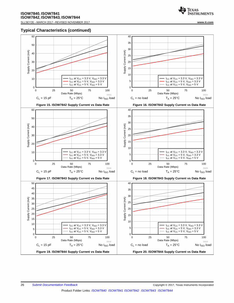
Typical Characteristics (continued)
CL = 15 pF TA = 25°C No IISO load
Figure 15. ISOW7842 Supply Current vs Data Rate
CL = no load TA = 25°C No IISO load
Figure 16. ISOW7842 Supply Current vs Data Rate
CL = 15 pF TA = 25°C No IISO load
Figure 17. ISOW7843 Supply Current vs Data Rate
CL = no load TA = 25°C No IISO load
Figure 18. ISOW7843 Supply Current vs Data Rate
CL = 15 pF TA = 25°C No IISO load
Figure 19. ISOW7844 Supply Current vs Data Rate
CL = no load TA = 25°C No IISO load
Figure 20. ISOW7844 Supply Current vs Data Rate

VISO = 3.3 V (50 mV/div)(1)
10 mA
110 mA
10 mA
2
100 µs/div
IISO VISO = 3.3 V (1 V/div)
ICC (40 mA/div)
2 ms/div
High-Level Output Current (mA)
Hig
h-Le
vel O
utpu
t Vol
tage
(V
)
-15 -10 -5 00
1
2
3
4
5
6
D015
VSO = 3.3 VVSO = 5 V
Low-Level Output Current (mA)
Low
-Lev
el O
utpu
t Vol
tage
(V
)
0 5 10 150
0.1
0.2
0.3
0.4
0.5
0.6
0.7
0.8
0.9
D016
VSO = 3.3 VVSO = 5 V
Free-Air Temperature (qC)
Pow
er S
uppl
y U
VLO
Thr
esho
ld (
V)
-40 -20 0 20 40 60 80 100 1202
2.1
2.2
2.3
2.4
2.5
2.6
VCC RisingVCC Falling
Free-Air Temperature (qC)
Pro
paga
tion
Del
ay T
ime
(ns)
-40 -20 0 20 40 60 80 100 1208
9
10
11
12
13
14
15
16
17
tPHL at VCC = 3.3 V, VISO = 3.3 VtPLH at VCC = 3.3 V, VISO = 3.3 VtPHL at VCC = 5 V, VISO = 3.3 VtPLH at VCC = 5 V, VISO = 3.3 VtPHL at VCC = 5 V, VISO = 5 VtPLH at VCC = 5 V, VISO = 5 V
27
ISOW7840, ISOW7841ISOW7842, ISOW7843, ISOW7844
www.ti.com SLLSEY2E –MARCH 2017–REVISED NOVEMBER 2017
Product Folder Links: ISOW7840 ISOW7841 ISOW7842 ISOW7843 ISOW7844
Submit Documentation FeedbackCopyright © 2017, Texas Instruments Incorporated
Typical Characteristics (continued)
Figure 21. Power-Supply Undervoltage Threshold vs FreeAir Temperature
Figure 22. Propagation Delay Time vs Free-Air Temperature
TA = 25°C
Figure 23. High-Level Output Voltage vs High-Level OutputCurrent
TA = 25°C
Figure 24. Low-Level Output Voltage vs Low-Level OutputCurrent
VCC = 5 V VISO = 3.3 VNegligible undershoot and overshoot because of load transient
Figure 25. 10-mA to 110-mA Load Transient Response
VCC = 5 V VISO = 3.3 VCurrent spike is because of charging the input supply capacitor
Figure 26. Soft Start at 10-mA Load

VISO = 3.3 V (20 mV/div)
5 µs/div
20 m
V
VISO = 5 V (20 mV/div)
5 µs/div
20 m
V
VISO = 5 V (1 V/div)
ICC (40 mA/div)
2 ms/div
VISO = 3.3 V (1 V/div)
ICC (40 mA/div)
2 ms/div
VISO = 5 V (1 V/div)
ICC (40 mA/div)
2 ms/div
28
ISOW7840, ISOW7841ISOW7842, ISOW7843, ISOW7844SLLSEY2E –MARCH 2017–REVISED NOVEMBER 2017 www.ti.com
Product Folder Links: ISOW7840 ISOW7841 ISOW7842 ISOW7843 ISOW7844
Submit Documentation Feedback Copyright © 2017, Texas Instruments Incorporated
Typical Characteristics (continued)
VCC = 5 V VISO = 3.3 VInput current spike is because of charging the input supply
decoupling capacitor
Figure 27. Soft Start at 120-mA Load
VCC = 5 V VISO = 5 VInput current spike is because of charging the input supply
decoupling capacitor
Figure 28. Soft Start at 10-mA Load
VCC = 5 V VISO = 5 VInput current spike is because of charging the input supply
decoupling capacitor
Figure 29. Soft Start at 130-mA Load
VCC = 5 V VISO = 5 V
Figure 30. VISO Ripple Voltage at 130 mA
VCC = 5 V VISO = 3.3 V
Figure 31. VISO Ripple Voltage at 130 mA

VSI
GNDI
IN
GNDI GNDO
OUT
VSO
0.1 �F10 �F
VCM± +
CL
C3 C4
5 V5 V
10 �F || 0.1 µF
IN OUT
CLSee Note B
VO
VI
VOL
VOH
VSI
0 V
trIs
ola
tio
n B
arr
ier
50 Input Generator
(See Note A) VI VO
tf
tPLH tPHL
50% 50%
50% 50%90%
10%
29
ISOW7840, ISOW7841ISOW7842, ISOW7843, ISOW7844
www.ti.com SLLSEY2E –MARCH 2017–REVISED NOVEMBER 2017
Product Folder Links: ISOW7840 ISOW7841 ISOW7842 ISOW7843 ISOW7844
Submit Documentation FeedbackCopyright © 2017, Texas Instruments Incorporated
8 Parameter Measurement Information
The input pulse is supplied by a generator having the following characteristics: PRR ≤ 50 kHz, 50% duty cycle, tr ≤ 3ns, tf ≤ 3 ns, ZO = 50 Ω. At the input, 50-Ω resistor is required to terminate the input generator signal. The resistor isnot required in the actual application.CL = 15 pF and includes instrumentation and fixture capacitance within ±20%.
Figure 32. Switching Characteristics Test Circuit and Voltage Waveforms
CL = 15 pF and includes instrumentation and fixture capacitance within ±20%.Pass-fail criteria: Outputs must remain stable.
Figure 33. Common-Mode Transient Immunity Test Circuit

30
ISOW7840, ISOW7841ISOW7842, ISOW7843, ISOW7844SLLSEY2E –MARCH 2017–REVISED NOVEMBER 2017 www.ti.com
Product Folder Links: ISOW7840 ISOW7841 ISOW7842 ISOW7843 ISOW7844
Submit Documentation Feedback Copyright © 2017, Texas Instruments Incorporated
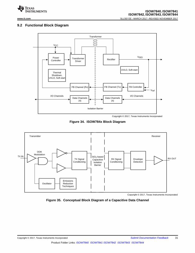
9 Detailed Description
9.1 OverviewThe ISOW784x family of devices comprises a high-efficiency, low-emissions isolated DC-DC converter and fourhigh-speed isolated data channels. Figure 34 shows the functional block diagram of the ISOW784x family ofdevices.
The integrated DC-DC converter uses switched mode operation and proprietary circuit techniques to reducepower losses and boost efficiency. Specialized control mechanisms, clocking schemes, and the use of a high-Qon-chip transformer provide high efficiency and low radiated emissions. The integrated transformer uses thin filmpolymer as the insulation barrier.
The VCC supply is provided to the primary power controller that switches the power stage connected to theintegrated transformer. Power is transferred to the secondary side, rectified and regulated to either 3.3 V or 5 V,depending on the SEL pin. The output voltage, VISO, is monitored and feedback information is conveyed to theprimary side through a dedicated isolation channel. The duty cycle of the primary switching stage is adjustedaccordingly. The fast feedback control loop of the power converter ensures low overshoots and undershootsduring load transients. Undervoltage lockout (UVLO) with hysteresis is integrated on the VCC and VISO supplieswhich ensures robust system performance under noisy conditions. An integrated soft-start mechanism ensurescontrolled inrush current and avoids any overshoot on the output during power up.
The integrated signal-isolation channels employ an ON-OFF keying (OOK) modulation scheme to transmit thedigital data across a silicon-dioxide based isolation barrier. The transmitter sends a high-frequency carrier acrossthe barrier to represent one state and sends no signal to represent the other state. The receiver demodulates thesignal after signal conditioning and produces the output through a buffer stage. The signal-isolation channelsincorporate advanced circuit techniques to maximize the CMTI performance and minimize the radiated emissionsfrom the high frequency carrier and IO buffer switching. Figure 35 shows a functional block diagram of a typicalsignal isolation channel.
The ISOW784x family of devices is suitable for applications that have limited board space and require moreintegration. These devices are also suitable for very-high voltage applications, where power transformersmeeting the required isolation specifications are bulky and expensive.
TX IN
Oscillator
OOK Modulation
Transmitter
Emissions Reduction
Techniques
TX Signal Conditioning
Envelope Detection
RX Signal Conditioning
Receiver
RX OUTSiO2 based Capacitive Isolation Barrier
Copyright © 2017, Texas Instruments Incorporated
Transformer
RectifierTransformerDriver
Power Controller
Thermal Shutdown,
UVLO, Soft-start
FB Channel (Rx)
Data Channels (4)
FB Channel (Tx)
Data Channels (4)
VCC
FB Controller
I/O Channels
Isolation Barrier
I/O Channels
UVLO, Soft-start
Vref
VISO
Copyright © 2017, Texas Instruments Incorporated
31
ISOW7840, ISOW7841ISOW7842, ISOW7843, ISOW7844
www.ti.com SLLSEY2E –MARCH 2017–REVISED NOVEMBER 2017
Product Folder Links: ISOW7840 ISOW7841 ISOW7842 ISOW7843 ISOW7844
Submit Documentation FeedbackCopyright © 2017, Texas Instruments Incorporated
9.2 Functional Block Diagram
Figure 34. ISOW784x Block Diagram
Figure 35. Conceptual Block Diagram of a Capacitive Data Channel

TX IN
RX OUT
Carrier signal through isolation barrier
32
ISOW7840, ISOW7841ISOW7842, ISOW7843, ISOW7844SLLSEY2E –MARCH 2017–REVISED NOVEMBER 2017 www.ti.com
Product Folder Links: ISOW7840 ISOW7841 ISOW7842 ISOW7843 ISOW7844
Submit Documentation Feedback Copyright © 2017, Texas Instruments Incorporated
Functional Block Diagram (continued)
(1) The F suffix is part of the orderable part number. See the Mechanical, Packaging, and Orderable Information section for the fullorderable part number.
(2) For detailed isolation ratings, see the Safety-Related Certifications table.
Figure 36 shows a conceptual detail of how the OOK scheme works.
Figure 36. On-Off Keying (OOK) Based Modulation Scheme
9.3 Feature DescriptionTable 1 provides an overview of the device features.
Table 1. Device Features
PART NUMBER (1) CHANNEL DIRECTION MAXIMUM DATA RATE DEFAULT OUTPUTSTATE RATED ISOLATION (2)
ISOW78404 forward, 0 reverse
100 Mbps
High
5 kVRMS / 7071 VPK
ISOW7840F LowISOW7841
3 forward, 1 reverseHigh
ISOW7841F LowISOW7842
2 forward, 2 reverseHigh
ISOW7842F LowISOW7843
1 forward, 3 reverseHigh
ISOW7843F LowISOW7844
0 forward, 4 reverseHigh
ISOW7844F Low
9.3.1 Electromagnetic Compatibility (EMC) ConsiderationsThe ISOW784x family of devices use emissions reduction schemes for the internal oscillator and advancedinternal layout scheme to minimize radiated emissions at the system level.
Many applications in harsh industrial environment are sensitive to disturbances such as electrostatic discharge(ESD), electrical fast transient (EFT), surge and electromagnetic emissions. These electromagnetic disturbancesare regulated by international standards such as IEC 61000-4-x and CISPR 22. Although system-levelperformance and reliability depends, to a large extent, on the application board design and layout, the ISOW784xfamily of devices incorporates many chip-level design improvements for overall system robustness. Some ofthese improvements include:• Robust ESD protection cells for input and output signal pins and inter-chip bond pads.• Low-resistance connectivity of ESD cells to supply and ground pins.• Enhanced performance of high voltage isolation capacitor for better tolerance of ESD, EFT and surge events.• Bigger on-chip decoupling capacitors to bypass undesirable high energy signals through a low impedance
path.

33
ISOW7840, ISOW7841ISOW7842, ISOW7843, ISOW7844
www.ti.com SLLSEY2E –MARCH 2017–REVISED NOVEMBER 2017
Product Folder Links: ISOW7840 ISOW7841 ISOW7842 ISOW7843 ISOW7844
Submit Documentation FeedbackCopyright © 2017, Texas Instruments Incorporated
• PMOS and NMOS devices isolated from each other by using guard rings to avoid triggering of parasiticSCRs.
• Reduced common mode currents across the isolation barrier by ensuring purely differential internal operation.
9.3.2 Power-Up and Power-Down BehaviorThe ISOW784x family of devices has built-in UVLO on the VCC and VISO supplies with positive-going andnegative-going thresholds and hysteresis. When the VCC voltage crosses the positive-going UVLO thresholdduring power-up, the DC-DC converter initializes and the power converter duty cycle is increased in a controlledmanner. This soft-start scheme limits primary peak currents drawn from the VCC supply and charges the VISOoutput in a controlled manner, avoiding overshoots. Outputs of the isolated data channels are in an indeterminatestate until the VCC or VISO voltage crosses the positive-going UVLO threshold. When the UVLO positive-goingthreshold is crossed on the secondary side VISO pin, the feedback data channel starts providing feedback to theprimary controller. The regulation loop takes over and the isolated data channels go to the normal state definedby the respective input channels or their default states. Design should consider a sufficient time margin (typically10 ms with 10-µF load capacitance) to allow this power up sequence before valid data channels are accountedfor system functionality.
When VCC power is lost, the primary side DC-DC controller turns off when the UVLO lower threshold is reached.The VISO capacitor then discharges depending on the external load. The isolated data outputs on the VISO sideare returned to the default state for the brief time that the VISO voltage takes to discharge to zero.
9.3.3 Current Limit, Thermal Overload ProtectionThe ISOW784x family of devices is protected against output overload and short circuit. Output voltage startsdropping when the power converter is not able to deliver the current demanded during overload conditions. For aVISO short-circuit to ground, the duty cycle of the converter is limited to help protect against any damage.
Thermal protection is also integrated to help prevent the device from getting damaged during overload and short-circuit conditions on the isolated output. Under these conditions, the device temperature starts to increase. Whenthe temperature goes above 180°C, thermal shutdown activates and the primary controller turns off whichremoves the energy supplied to the VISO load, which causes the device to cool off. When the junctiontemperature goes below 150°C, the device starts to function normally. If an overload or output short-circuitcondition prevails, this protection cycle is repeated. Care should be taken in the design to prevent the devicejunction temperatures from reaching such high values.
9.4 Device Functional ModesTable 2 lists the supply configurations for these devices.
(1) VCC = 3.3 V, SEL shorted to VISO (essentially VISO = 5 V) is not recommended mode of configuration.(2) The SEL pin has a weak pulldown internally. Therefore for VISO = 3.3 V, the SEL pin should be
strongly connected to the GND2 pin in noisy system scenarios.
Table 2. Supply ConfigurationsSEL INPUT VCC VISO
Shorted to VISO 5 V 5 VShorted to GND2 or floating 5 V 3.3 VShorted to GND2 or floating 3.3 V (1) 3.3 V (2)

Input (Devices without F suffix) Input (Devices with F suffix)
Output SEL Pin
INx
VCC VCC VCC VCC
985
1.5 M
INx
VCC VCC VCC
985
1.5 M
SEL
VISO VISO VISO
1970
2 M
VISO
OUTx~20
34
ISOW7840, ISOW7841ISOW7842, ISOW7843, ISOW7844SLLSEY2E –MARCH 2017–REVISED NOVEMBER 2017 www.ti.com
Product Folder Links: ISOW7840 ISOW7841 ISOW7842 ISOW7843 ISOW7844
Submit Documentation Feedback Copyright © 2017, Texas Instruments Incorporated
(1) PU = Powered up (VCC ≥ 2.7 V); PD = Powered down (VCC < 2.1 V); X = Irrelevant; H = High level; L = Low level, VCC = Input-sidesupply
(2) In the default condition, the output is high for ISOW784x and low for ISOW784x with the F suffix.(3) The outputs are in an undetermined state when VCC < 2.1 V.
Table 3 lists the functional modes for ISOW784x devices.
Table 3. Function Table (1)
INPUT SUPPLY(VCC)
INPUT(INx)
OUTPUT(OUTx) COMMENTS
PU
H HOutput channel assumes the logic state of its input
L L
Open DefaultDefault mode (2): When INx is open, the correspondingoutput channel assumes logic based on default outputmode of selected version
PD x Undetermined (3)
9.4.1 Device I/O Schematics
Figure 37. Device I/O Schematics
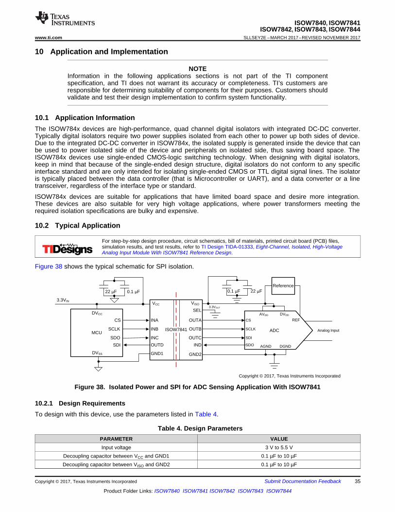
MCUISOW7841
VCC
IND
SEL
GND2
INA
INB
INC
OUTD
GND1
OUTA
OUTB
OUTC
VISO
ADC
SDO
SCLK
CS
SDI
CS
SCLK
SDI
SDO
AVDD DVDD
REF
AGND DGND
DVCC
DVSS
3.3VIN
3.3VOUT
Analog Input
0.1 �F22 �F 22 �F0.1 �FReference
Copyright © 2017, Texas Instruments Incorporated
35
ISOW7840, ISOW7841ISOW7842, ISOW7843, ISOW7844
www.ti.com SLLSEY2E –MARCH 2017–REVISED NOVEMBER 2017
Product Folder Links: ISOW7840 ISOW7841 ISOW7842 ISOW7843 ISOW7844
Submit Documentation FeedbackCopyright © 2017, Texas Instruments Incorporated
10 Application and Implementation
NOTEInformation in the following applications sections is not part of the TI componentspecification, and TI does not warrant its accuracy or completeness. TI’s customers areresponsible for determining suitability of components for their purposes. Customers shouldvalidate and test their design implementation to confirm system functionality.
10.1 Application InformationThe ISOW784x devices are high-performance, quad channel digital isolators with integrated DC-DC converter.Typically digital isolators require two power supplies isolated from each other to power up both sides of device.Due to the integrated DC-DC converter in ISOW784x, the isolated supply is generated inside the device that canbe used to power isolated side of the device and peripherals on isolated side, thus saving board space. TheISOW784x devices use single-ended CMOS-logic switching technology. When designing with digital isolators,keep in mind that because of the single-ended design structure, digital isolators do not conform to any specificinterface standard and are only intended for isolating single-ended CMOS or TTL digital signal lines. The isolatoris typically placed between the data controller (that is Microcontroller or UART), and a data converter or a linetransceiver, regardless of the interface type or standard.
ISOW784x devices are suitable for applications that have limited board space and desire more integration.These devices are also suitable for very high voltage applications, where power transformers meeting therequired isolation specifications are bulky and expensive.
10.2 Typical Application
For step-by-step design procedure, circuit schematics, bill of materials, printed circuit board (PCB) files,simulation results, and test results, refer to TI Design TIDA-01333, Eight-Channel, Isolated, High-VoltageAnalog Input Module With ISOW7841 Reference Design.
Figure 38 shows the typical schematic for SPI isolation.
Figure 38. Isolated Power and SPI for ADC Sensing Application With ISOW7841
10.2.1 Design RequirementsTo design with this device, use the parameters listed in Table 4.
Table 4. Design ParametersPARAMETER VALUEInput voltage 3 V to 5.5 V
Decoupling capacitor between VCC and GND1 0.1 µF to 10 µFDecoupling capacitor between VISO and GND2 0.1 µF to 10 µF

1
2
3
4
5
7
8
16
15
14
13
12
10
9
INB
SEL
OUTB
VISO
GND1
VCC
GND2
INA OUTA
INC OUTC
2 mm Maximum from Vcc
GND1
2 mm Maximum from VISO
10 �F
0.1 �F
GND2
11 IND6OUTD
10 �F
0.1 �F
36
ISOW7840, ISOW7841ISOW7842, ISOW7843, ISOW7844SLLSEY2E –MARCH 2017–REVISED NOVEMBER 2017 www.ti.com
Product Folder Links: ISOW7840 ISOW7841 ISOW7842 ISOW7843 ISOW7844
Submit Documentation Feedback Copyright © 2017, Texas Instruments Incorporated
Because of very-high current flowing through the ISOW7841 VCC and VISO supplies, higher decoupling capacitorstypically provide better noise and ripple performance. Although a 10-µF capacitor is adequate, higher decouplingcapacitors (such as 47 µF) on both the VCC and VISO pins to the respective grounds are strongly recommendedto achieve the best performance.
10.2.2 Detailed Design ProcedureThe ISOW784x family of devices only requires external bypass capacitors to operate. These low-ESR ceramicbypass capacitors must be placed as close to the chip pads as possible.
Figure 39. Typical ISOW7841 Circuit Hook-Up
The VCC power-supply input provides power to isolated data channels and to the isolated DC-DC converter. UseEquation 1 to calculate the total power budget on the primary side.
ICC = (VISO × IISO) / (η × VCC) + Iinpx
where• ICC is the total current required by the primary supply.• VISO is the isolated supply voltage.• IISO is the external load on the isolated supply voltage.• η is the efficiency.• VCC is the supply voltage.• Iinpx is the total current drawn for the isolated data channels and power converter when data channels are
toggling at a specific data rate. This data is shown in the Electrical Characteristics—5-V Input, 5-V Outputtable. (1)

ICC (40 mA/div)
VISO (600 mV/div)
37
ISOW7840, ISOW7841ISOW7842, ISOW7843, ISOW7844
www.ti.com SLLSEY2E –MARCH 2017–REVISED NOVEMBER 2017
Product Folder Links: ISOW7840 ISOW7841 ISOW7842 ISOW7843 ISOW7844
Submit Documentation FeedbackCopyright © 2017, Texas Instruments Incorporated
10.2.3 Application Curve
VCC = 3.3 V IISO = 70 mAInput current spike is because of charging the input supply decoupling capacitor
Figure 40. Soft-Start Waveform
11 Power Supply RecommendationsTo help ensure reliable operation at data rates and supply voltages, adequate decoupling capacitors must belocated as close to supply pins as possible. The input supply must have an appropriate current rating to supportoutput load and switching at the maximum data rate required by the end application. For more information, referto the Detailed Design Procedure section.

38
ISOW7840, ISOW7841ISOW7842, ISOW7843, ISOW7844SLLSEY2E –MARCH 2017–REVISED NOVEMBER 2017 www.ti.com
Product Folder Links: ISOW7840 ISOW7841 ISOW7842 ISOW7843 ISOW7844
Submit Documentation Feedback Copyright © 2017, Texas Instruments Incorporated
12 Layout
12.1 Layout GuidelinesA minimum of four layers is required to accomplish a low-EMI PCB design (see Figure 41). Layer stacking shouldbe in the following order (top-to-bottom): high-speed signal layer, ground plane, power plane, and low-frequencysignal layer.• Routing the high-speed traces on the top layer avoids the use of vias (and the introduction of their
inductances) and allows for clean interconnects between the isolator and the transmitter and receiver circuitsof the data link.
• Placing a solid ground plane next to the high-speed signal layer establishes controlled impedance fortransmission line interconnects and provides an excellent low-inductance path for the return current flow.
• Placing the power plane next to the ground plane creates additional high-frequency bypass capacitance ofapproximately 100 pF/in2.
• Routing the slower speed control signals on the bottom layer allows for greater flexibility as these signal linksusually have margin to tolerate discontinuities such as vias.
• Keep decoupling capacitors as close as possible to the VCC and VISO pins.
If an additional supply voltage plane or signal layer is needed, add a second power or ground plane system tothe stack to keep it symmetrical. This makes the stack mechanically stable and prevents it from warping. Also thepower and ground plane of each power system can be placed closer together, thus increasing the high-frequencybypass capacitance significantly.
Because the device has no thermal pad to dissipate heat, the device dissipates heat through the respective GNDpins. Ensure that enough copper is present on both GND pins to prevent the internal junction temperature of thedevice from rising to unacceptable levels.
The ISOW784x integrated signal and power isolation device simplifies system design and reduces board area.The use of low-inductance micro-transformers in the ISOW784x device necessitates the use of high frequencyswitching, resulting in higher radiated emissions compared to discrete solutions. The ISOW784x device uses on-chip circuit techniques to reduce emissions compared to competing solutions. For further reduction in radiatedemissions at system level, refer to the Low-Emission Designs With ISOW7841 Integrated Signal and PowerIsolator application report.
12.1.1 PCB MaterialFor digital circuit boards operating at less than 150 Mbps, (or rise and fall times greater than 1 ns), and tracelengths of up to 10 inches, use standard FR-4 UL94V-0 printed circuit board. This PCB is preferred over cheaperalternatives because of lower dielectric losses at high frequencies, less moisture absorption, greater strength andstiffness, and the self-extinguishing flammability-characteristics.
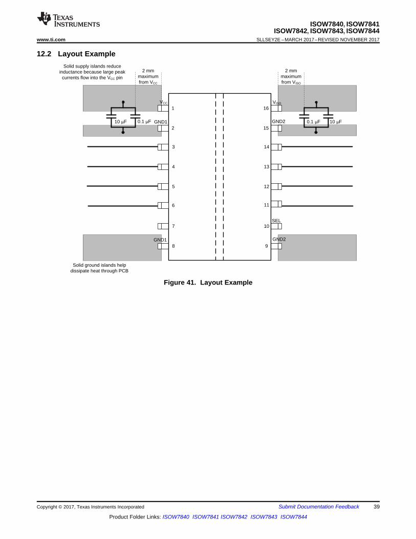
2 mm maximum from VISO
Solid ground islands help dissipate heat through PCB
Solid supply islands reduce inductance because large peak
currents flow into the VCC pin
1
2
3
4
5
7
8
16
15
14
13
12
10
9
SEL
VISO
GND1
VCC
GND2
GND1 GND2
116
0.1 �F 10 �F10 �F 0.1 �F
2 mm maximum from VCC
39
ISOW7840, ISOW7841ISOW7842, ISOW7843, ISOW7844
www.ti.com SLLSEY2E –MARCH 2017–REVISED NOVEMBER 2017
Product Folder Links: ISOW7840 ISOW7841 ISOW7842 ISOW7843 ISOW7844
Submit Documentation FeedbackCopyright © 2017, Texas Instruments Incorporated
12.2 Layout Example
Figure 41. Layout Example

40
ISOW7840, ISOW7841ISOW7842, ISOW7843, ISOW7844SLLSEY2E –MARCH 2017–REVISED NOVEMBER 2017 www.ti.com
Product Folder Links: ISOW7840 ISOW7841 ISOW7842 ISOW7843 ISOW7844
Submit Documentation Feedback Copyright © 2017, Texas Instruments Incorporated
13 Device and Documentation Support
13.1 Device Support
13.1.1 Development SupportFor development support, refer to:• 8-ch Isolated High Voltage Analog Input Module with ISOW7841 Reference Design• Isolated RS-485 With Integrated Signal and Power Reference Design• Isolated RS-232 With Integrated Signal and Power Reference Design
13.2 Documentation Support
13.2.1 Related DocumentationFor related documentation see the following:• Texas Instruments, Digital Isolator Design Guide• Texas Instruments, Isolation Glossary• Texas Instruments, ISOW784x Quad-Channel Digital Isolator With Integrated DC-DC Converter Evaluation
Module user's guide• Texas Instruments, Low-Emission Designs With ISOW7841 Integrated Signal and Power Isolator application
report
13.3 Related LinksThe table below lists quick access links. Categories include technical documents, support and communityresources, tools and software, and quick access to sample or buy.
Table 5. Related Links
PARTS PRODUCT FOLDER ORDER NOW TECHNICALDOCUMENTS
TOOLS &SOFTWARE
SUPPORT &COMMUNITY
ISOW7840 Click here Click here Click here Click here Click hereISOW7841 Click here Click here Click here Click here Click hereISOW7842 Click here Click here Click here Click here Click hereISOW7843 Click here Click here Click here Click here Click hereISOW7844 Click here Click here Click here Click here Click here
13.4 Receiving Notification of Documentation UpdatesTo receive notification of documentation updates, navigate to the device product folder on ti.com. In the upperright corner, click on Alert me to register and receive a weekly digest of any product information that haschanged. For change details, review the revision history included in any revised document.
13.5 Community ResourcesThe following links connect to TI community resources. Linked contents are provided "AS IS" by the respectivecontributors. They do not constitute TI specifications and do not necessarily reflect TI's views; see TI's Terms ofUse.
TI E2E™ Online Community TI's Engineer-to-Engineer (E2E) Community. Created to foster collaborationamong engineers. At e2e.ti.com, you can ask questions, share knowledge, explore ideas and helpsolve problems with fellow engineers.
Design Support TI's Design Support Quickly find helpful E2E forums along with design support tools andcontact information for technical support.
13.6 TrademarksE2E is a trademark of Texas Instruments.All other trademarks are the property of their respective owners.
41
ISOW7840, ISOW7841ISOW7842, ISOW7843, ISOW7844
www.ti.com SLLSEY2E –MARCH 2017–REVISED NOVEMBER 2017
Product Folder Links: ISOW7840 ISOW7841 ISOW7842 ISOW7843 ISOW7844
Submit Documentation FeedbackCopyright © 2017, Texas Instruments Incorporated
13.7 Electrostatic Discharge CautionThis integrated circuit can be damaged by ESD. Texas Instruments recommends that all integrated circuits be handled withappropriate precautions. Failure to observe proper handling and installation procedures can cause damage.
ESD damage can range from subtle performance degradation to complete device failure. Precision integrated circuits may be moresusceptible to damage because very small parametric changes could cause the device not to meet its published specifications.
13.8 GlossarySLYZ022 — TI Glossary.
This glossary lists and explains terms, acronyms, and definitions.
14 Mechanical, Packaging, and Orderable InformationThe following pages include mechanical, packaging, and orderable information. This information is the mostcurrent data available for the designated devices. This data is subject to change without notice and revision ofthis document. For browser-based versions of this data sheet, refer to the left-hand navigation.

PACKAGE OPTION ADDENDUM
www.ti.com 2-Dec-2017
Addendum-Page 1
PACKAGING INFORMATION
Orderable Device Status(1)
Package Type PackageDrawing
Pins PackageQty
Eco Plan(2)
Lead/Ball Finish(6)
MSL Peak Temp(3)
Op Temp (°C) Device Marking(4/5)
Samples
ISOW7840DWE ACTIVE SOIC DWE 16 40 Green (RoHS& no Sb/Br)
CU NIPDAU Level-3-260C-168 HR -40 to 125 ISOW7840
ISOW7840DWER ACTIVE SOIC DWE 16 2000 Green (RoHS& no Sb/Br)
CU NIPDAU Level-3-260C-168 HR -40 to 125 ISOW7840
ISOW7840FDWE ACTIVE SOIC DWE 16 40 Green (RoHS& no Sb/Br)
CU NIPDAU Level-3-260C-168 HR -40 to 125 ISOW7840F
ISOW7840FDWER ACTIVE SOIC DWE 16 2000 Green (RoHS& no Sb/Br)
CU NIPDAU Level-3-260C-168 HR -40 to 125 ISOW7840F
ISOW7841DWE ACTIVE SOIC DWE 16 40 Green (RoHS& no Sb/Br)
CU NIPDAU Level-3-260C-168 HR -40 to 125 ISOW7841
ISOW7841DWER ACTIVE SOIC DWE 16 2000 Green (RoHS& no Sb/Br)
CU NIPDAU Level-3-260C-168 HR -40 to 125 ISOW7841
ISOW7841FDWE ACTIVE SOIC DWE 16 40 Green (RoHS& no Sb/Br)
CU NIPDAU Level-3-260C-168 HR -40 to 125 ISOW7841F
ISOW7841FDWER ACTIVE SOIC DWE 16 2000 Green (RoHS& no Sb/Br)
CU NIPDAU Level-3-260C-168 HR -40 to 125 ISOW7841F
ISOW7842DWE ACTIVE SOIC DWE 16 40 Green (RoHS& no Sb/Br)
CU NIPDAU Level-3-260C-168 HR -40 to 125 ISOW7842
ISOW7842DWER ACTIVE SOIC DWE 16 2000 Green (RoHS& no Sb/Br)
CU NIPDAU Level-3-260C-168 HR -40 to 125 ISOW7842
ISOW7842FDWE ACTIVE SOIC DWE 16 40 Green (RoHS& no Sb/Br)
CU NIPDAU Level-3-260C-168 HR -40 to 125 ISOW7842F
ISOW7842FDWER ACTIVE SOIC DWE 16 2000 Green (RoHS& no Sb/Br)
CU NIPDAU Level-3-260C-168 HR -40 to 125 ISOW7842F
ISOW7843DWE ACTIVE SOIC DWE 16 40 Green (RoHS& no Sb/Br)
CU NIPDAU Level-3-260C-168 HR -40 to 125 ISOW7843
ISOW7843DWER ACTIVE SOIC DWE 16 2000 Green (RoHS& no Sb/Br)
CU NIPDAU Level-3-260C-168 HR -40 to 125 ISOW7843
ISOW7843FDWE ACTIVE SOIC DWE 16 40 Green (RoHS& no Sb/Br)
CU NIPDAU Level-3-260C-168 HR -40 to 125 ISOW7843F
ISOW7843FDWER ACTIVE SOIC DWE 16 2000 Green (RoHS& no Sb/Br)
CU NIPDAU Level-3-260C-168 HR -40 to 125 ISOW7843F
ISOW7844DWE ACTIVE SOIC DWE 16 40 Green (RoHS& no Sb/Br)
CU NIPDAU Level-3-260C-168 HR -40 to 125 ISOW7844

PACKAGE OPTION ADDENDUM
www.ti.com 2-Dec-2017
Addendum-Page 2
Orderable Device Status(1)
Package Type PackageDrawing
Pins PackageQty
Eco Plan(2)
Lead/Ball Finish(6)
MSL Peak Temp(3)
Op Temp (°C) Device Marking(4/5)
Samples
ISOW7844DWER ACTIVE SOIC DWE 16 2000 Green (RoHS& no Sb/Br)
CU NIPDAU Level-3-260C-168 HR -40 to 125 ISOW7844
ISOW7844FDWE ACTIVE SOIC DWE 16 40 Green (RoHS& no Sb/Br)
CU NIPDAU Level-3-260C-168 HR -40 to 125 ISOW7844F
ISOW7844FDWER ACTIVE SOIC DWE 16 2000 Green (RoHS& no Sb/Br)
CU NIPDAU Level-3-260C-168 HR -40 to 125 ISOW7844F
(1) The marketing status values are defined as follows:ACTIVE: Product device recommended for new designs.LIFEBUY: TI has announced that the device will be discontinued, and a lifetime-buy period is in effect.NRND: Not recommended for new designs. Device is in production to support existing customers, but TI does not recommend using this part in a new design.PREVIEW: Device has been announced but is not in production. Samples may or may not be available.OBSOLETE: TI has discontinued the production of the device.
(2) RoHS: TI defines "RoHS" to mean semiconductor products that are compliant with the current EU RoHS requirements for all 10 RoHS substances, including the requirement that RoHS substancedo not exceed 0.1% by weight in homogeneous materials. Where designed to be soldered at high temperatures, "RoHS" products are suitable for use in specified lead-free processes. TI mayreference these types of products as "Pb-Free".RoHS Exempt: TI defines "RoHS Exempt" to mean products that contain lead but are compliant with EU RoHS pursuant to a specific EU RoHS exemption.Green: TI defines "Green" to mean the content of Chlorine (Cl) and Bromine (Br) based flame retardants meet JS709B low halogen requirements of <=1000ppm threshold. Antimony trioxide basedflame retardants must also meet the <=1000ppm threshold requirement.
(3) MSL, Peak Temp. - The Moisture Sensitivity Level rating according to the JEDEC industry standard classifications, and peak solder temperature.
(4) There may be additional marking, which relates to the logo, the lot trace code information, or the environmental category on the device.
(5) Multiple Device Markings will be inside parentheses. Only one Device Marking contained in parentheses and separated by a "~" will appear on a device. If a line is indented then it is a continuationof the previous line and the two combined represent the entire Device Marking for that device.
(6) Lead/Ball Finish - Orderable Devices may have multiple material finish options. Finish options are separated by a vertical ruled line. Lead/Ball Finish values may wrap to two lines if the finishvalue exceeds the maximum column width.
Important Information and Disclaimer:The information provided on this page represents TI's knowledge and belief as of the date that it is provided. TI bases its knowledge and belief on informationprovided by third parties, and makes no representation or warranty as to the accuracy of such information. Efforts are underway to better integrate information from third parties. TI has taken andcontinues to take reasonable steps to provide representative and accurate information but may not have conducted destructive testing or chemical analysis on incoming materials and chemicals.TI and TI suppliers consider certain information to be proprietary, and thus CAS numbers and other limited information may not be available for release.
In no event shall TI's liability arising out of such information exceed the total purchase price of the TI part(s) at issue in this document sold by TI to Customer on an annual basis.
PACKAGE OPTION ADDENDUM
www.ti.com 2-Dec-2017
Addendum-Page 3

TAPE AND REEL INFORMATION
*All dimensions are nominal
Device PackageType
PackageDrawing
Pins SPQ ReelDiameter
(mm)
ReelWidth
W1 (mm)
A0(mm)
B0(mm)
K0(mm)
P1(mm)
W(mm)
Pin1Quadrant
ISOW7840DWER SOIC DWE 16 2000 330.0 16.4 10.75 10.7 2.7 12.0 16.0 Q1
ISOW7840FDWER SOIC DWE 16 2000 330.0 16.4 10.75 10.7 2.7 12.0 16.0 Q1
ISOW7841DWER SOIC DWE 16 2000 330.0 16.4 10.75 10.7 2.7 12.0 16.0 Q1
ISOW7841FDWER SOIC DWE 16 2000 330.0 16.4 10.75 10.7 2.7 12.0 16.0 Q1
ISOW7842DWER SOIC DWE 16 2000 330.0 16.4 10.75 10.7 2.7 12.0 16.0 Q1
ISOW7842FDWER SOIC DWE 16 2000 330.0 16.4 10.75 10.7 2.7 12.0 16.0 Q1
ISOW7843DWER SOIC DWE 16 2000 330.0 16.4 10.75 10.7 2.7 12.0 16.0 Q1
ISOW7843FDWER SOIC DWE 16 2000 330.0 16.4 10.75 10.7 2.7 12.0 16.0 Q1
ISOW7844DWER SOIC DWE 16 2000 330.0 16.4 10.75 10.7 2.7 12.0 16.0 Q1
ISOW7844FDWER SOIC DWE 16 2000 330.0 16.4 10.75 10.7 2.7 12.0 16.0 Q1
PACKAGE MATERIALS INFORMATION
www.ti.com 22-Nov-2017
Pack Materials-Page 1

*All dimensions are nominal
Device Package Type Package Drawing Pins SPQ Length (mm) Width (mm) Height (mm)
ISOW7840DWER SOIC DWE 16 2000 367.0 367.0 38.0
ISOW7840FDWER SOIC DWE 16 2000 367.0 367.0 38.0
ISOW7841DWER SOIC DWE 16 2000 367.0 367.0 38.0
ISOW7841FDWER SOIC DWE 16 2000 367.0 367.0 38.0
ISOW7842DWER SOIC DWE 16 2000 367.0 367.0 38.0
ISOW7842FDWER SOIC DWE 16 2000 367.0 367.0 38.0
ISOW7843DWER SOIC DWE 16 2000 367.0 367.0 38.0
ISOW7843FDWER SOIC DWE 16 2000 367.0 367.0 38.0
ISOW7844DWER SOIC DWE 16 2000 367.0 367.0 38.0
ISOW7844FDWER SOIC DWE 16 2000 367.0 367.0 38.0
PACKAGE MATERIALS INFORMATION
www.ti.com 22-Nov-2017
Pack Materials-Page 2

www.ti.com
PACKAGE OUTLINE
C
TYP10.639.97
2.65 MAX
14X 1.27
16X 0.510.31
2X8.89
TYP0.330.10
0 - 80.30.1
(1.4)
0.25GAGE PLANE
1.270.40
A
NOTE 3
10.510.1
BNOTE 4
7.67.4
4223098/A 07/2016
SOIC - 2.65 mm max heightDWE0016ASOIC
NOTES: 1. All linear dimensions are in millimeters. Any dimensions in parenthesis are for reference only. Dimensioning and tolerancing per ASME Y14.5M. 2. This drawing is subject to change without notice. 3. This dimension does not include mold flash, protrusions, or gate burrs. Mold flash, protrusions, or gate burrs shall not exceed 0.15 mm, per side. 4. This dimension does not include interlead flash. Interlead flash shall not exceed 0.25 mm, per side.5. Reference JEDEC registration MS-013.
1 16
0.25 C A B
98
PIN 1 IDAREA
SEATING PLANE
0.1 C
SEE DETAIL A
DETAIL ATYPICAL
SCALE 1.500

www.ti.com
EXAMPLE BOARD LAYOUT
(9.75)
0.07 MAXALL AROUND
0.07 MINALL AROUND
(9.3)
14X (1.27)
16X (1.65)
16X (0.6)
14X (1.27)
16X (2)
16X (0.6)
4223098/A 07/2016
SOIC - 2.65 mm max heightDWE0016ASOIC
SYMM
SYMM
SEEDETAILS
1
8 9
16
SYMM
HV / ISOLATION OPTION8.1 mm CLEARANCE/CREEPAGE
NOTES: (continued) 6. Publication IPC-7351 may have alternate designs. 7. Solder mask tolerances between and around signal pads can vary based on board fabrication site.
METAL SOLDER MASKOPENING
NON SOLDER MASKDEFINED
SOLDER MASK DETAILS
OPENINGSOLDER MASK METAL
SOLDER MASKDEFINED
LAND PATTERN EXAMPLESCALE:4X
SYMM
1
8 9
16
IPC-7351 NOMINAL7.3 mm CLEARANCE/CREEPAGE
SEEDETAILS

www.ti.com
EXAMPLE STENCIL DESIGN
16X (1.65)
16X (0.6)
14X (1.27)
(9.75)
16X (2)
16X (0.6)
14X (1.27)
(9.3)
4223098/A 07/2016
SOIC - 2.65 mm max heightDWE0016ASOIC
NOTES: (continued) 8. Laser cutting apertures with trapezoidal walls and rounded corners may offer better paste release. IPC-7525 may have alternate design recommendations. 9. Board assembly site may have different recommendations for stencil design.
SYMM
SYMM
1
8 9
16
HV / ISOLATION OPTION8.1 mm CLEARANCE/CREEPAGE
SOLDER PASTE EXAMPLEBASED ON 0.125 mm THICK STENCIL
SCALE:4X
SYMM
SYMM
1
8 9
16
IPC-7351 NOMINAL7.3 mm CLEARANCE/CREEPAGE

IMPORTANT NOTICE
Texas Instruments Incorporated (TI) reserves the right to make corrections, enhancements, improvements and other changes to itssemiconductor products and services per JESD46, latest issue, and to discontinue any product or service per JESD48, latest issue. Buyersshould obtain the latest relevant information before placing orders and should verify that such information is current and complete.TI’s published terms of sale for semiconductor products (http://www.ti.com/sc/docs/stdterms.htm) apply to the sale of packaged integratedcircuit products that TI has qualified and released to market. Additional terms may apply to the use or sale of other types of TI products andservices.Reproduction of significant portions of TI information in TI data sheets is permissible only if reproduction is without alteration and isaccompanied by all associated warranties, conditions, limitations, and notices. TI is not responsible or liable for such reproduceddocumentation. Information of third parties may be subject to additional restrictions. Resale of TI products or services with statementsdifferent from or beyond the parameters stated by TI for that product or service voids all express and any implied warranties for theassociated TI product or service and is an unfair and deceptive business practice. TI is not responsible or liable for any such statements.Buyers and others who are developing systems that incorporate TI products (collectively, “Designers”) understand and agree that Designersremain responsible for using their independent analysis, evaluation and judgment in designing their applications and that Designers havefull and exclusive responsibility to assure the safety of Designers' applications and compliance of their applications (and of all TI productsused in or for Designers’ applications) with all applicable regulations, laws and other applicable requirements. Designer represents that, withrespect to their applications, Designer has all the necessary expertise to create and implement safeguards that (1) anticipate dangerousconsequences of failures, (2) monitor failures and their consequences, and (3) lessen the likelihood of failures that might cause harm andtake appropriate actions. Designer agrees that prior to using or distributing any applications that include TI products, Designer willthoroughly test such applications and the functionality of such TI products as used in such applications.TI’s provision of technical, application or other design advice, quality characterization, reliability data or other services or information,including, but not limited to, reference designs and materials relating to evaluation modules, (collectively, “TI Resources”) are intended toassist designers who are developing applications that incorporate TI products; by downloading, accessing or using TI Resources in anyway, Designer (individually or, if Designer is acting on behalf of a company, Designer’s company) agrees to use any particular TI Resourcesolely for this purpose and subject to the terms of this Notice.TI’s provision of TI Resources does not expand or otherwise alter TI’s applicable published warranties or warranty disclaimers for TIproducts, and no additional obligations or liabilities arise from TI providing such TI Resources. TI reserves the right to make corrections,enhancements, improvements and other changes to its TI Resources. TI has not conducted any testing other than that specificallydescribed in the published documentation for a particular TI Resource.Designer is authorized to use, copy and modify any individual TI Resource only in connection with the development of applications thatinclude the TI product(s) identified in such TI Resource. NO OTHER LICENSE, EXPRESS OR IMPLIED, BY ESTOPPEL OR OTHERWISETO ANY OTHER TI INTELLECTUAL PROPERTY RIGHT, AND NO LICENSE TO ANY TECHNOLOGY OR INTELLECTUAL PROPERTYRIGHT OF TI OR ANY THIRD PARTY IS GRANTED HEREIN, including but not limited to any patent right, copyright, mask work right, orother intellectual property right relating to any combination, machine, or process in which TI products or services are used. Informationregarding or referencing third-party products or services does not constitute a license to use such products or services, or a warranty orendorsement thereof. Use of TI Resources may require a license from a third party under the patents or other intellectual property of thethird party, or a license from TI under the patents or other intellectual property of TI.TI RESOURCES ARE PROVIDED “AS IS” AND WITH ALL FAULTS. TI DISCLAIMS ALL OTHER WARRANTIES ORREPRESENTATIONS, EXPRESS OR IMPLIED, REGARDING RESOURCES OR USE THEREOF, INCLUDING BUT NOT LIMITED TOACCURACY OR COMPLETENESS, TITLE, ANY EPIDEMIC FAILURE WARRANTY AND ANY IMPLIED WARRANTIES OFMERCHANTABILITY, FITNESS FOR A PARTICULAR PURPOSE, AND NON-INFRINGEMENT OF ANY THIRD PARTY INTELLECTUALPROPERTY RIGHTS. TI SHALL NOT BE LIABLE FOR AND SHALL NOT DEFEND OR INDEMNIFY DESIGNER AGAINST ANY CLAIM,INCLUDING BUT NOT LIMITED TO ANY INFRINGEMENT CLAIM THAT RELATES TO OR IS BASED ON ANY COMBINATION OFPRODUCTS EVEN IF DESCRIBED IN TI RESOURCES OR OTHERWISE. IN NO EVENT SHALL TI BE LIABLE FOR ANY ACTUAL,DIRECT, SPECIAL, COLLATERAL, INDIRECT, PUNITIVE, INCIDENTAL, CONSEQUENTIAL OR EXEMPLARY DAMAGES INCONNECTION WITH OR ARISING OUT OF TI RESOURCES OR USE THEREOF, AND REGARDLESS OF WHETHER TI HAS BEENADVISED OF THE POSSIBILITY OF SUCH DAMAGES.Unless TI has explicitly designated an individual product as meeting the requirements of a particular industry standard (e.g., ISO/TS 16949and ISO 26262), TI is not responsible for any failure to meet such industry standard requirements.Where TI specifically promotes products as facilitating functional safety or as compliant with industry functional safety standards, suchproducts are intended to help enable customers to design and create their own applications that meet applicable functional safety standardsand requirements. Using products in an application does not by itself establish any safety features in the application. Designers mustensure compliance with safety-related requirements and standards applicable to their applications. Designer may not use any TI products inlife-critical medical equipment unless authorized officers of the parties have executed a special contract specifically governing such use.Life-critical medical equipment is medical equipment where failure of such equipment would cause serious bodily injury or death (e.g., lifesupport, pacemakers, defibrillators, heart pumps, neurostimulators, and implantables). Such equipment includes, without limitation, allmedical devices identified by the U.S. Food and Drug Administration as Class III devices and equivalent classifications outside the U.S.TI may expressly designate certain products as completing a particular qualification (e.g., Q100, Military Grade, or Enhanced Product).Designers agree that it has the necessary expertise to select the product with the appropriate qualification designation for their applicationsand that proper product selection is at Designers’ own risk. Designers are solely responsible for compliance with all legal and regulatoryrequirements in connection with such selection.Designer will fully indemnify TI and its representatives against any damages, costs, losses, and/or liabilities arising out of Designer’s non-compliance with the terms and provisions of this Notice.
Mailing Address: Texas Instruments, Post Office Box 655303, Dallas, Texas 75265Copyright © 2017, Texas Instruments Incorporated