isolated sleepy keeper approach: an effective sleep state ... · approach in low leakage power,...
TRANSCRIPT

International Research Journal of Engineering and Technology (IRJET) e-ISSN: 2395 -0056
Volume: 03 Issue: 05 | May-2016 www.irjet.net p-ISSN: 2395-0072
© 2016, IRJET | Impact Factor value: 4.45 | ISO 9001:2008 Certified Journal | Page 951
Isolated Sleepy Keeper Approach: An Effective Sleep State Approach in Low leakage Power, VLSI Design
Sainiranjan Muchakayala1, Owais Shah2
1MTech VLSI ,Department of Electronics ,Noida International University Greater Noida ,UP 2Asst. Professor Department of Electronics, Noida International University Greater Noida ,UP
---------------------------------------------------------------------***-------------------------------------------------------------------
Abstract - Today there is no need to explain the necessity of having low power dissipation devices .To realize this objective a number of ways have been explored at various levels of design. At the other end , high demand to have a greater performance continuously drive the design world to scale down to a few nanometers .The scaling down process has the side effect of decreased threshold voltage , which in turn increases the sub threshold leakage current. There are various techniques proposed to decrease this sub threshold leakage current. Sleepy keeper is a method to realize this even with retaining the output in the sleep state, but it can’t retain the output in case of disturbances in the input. Here we introduce a method which can sustain these input disturbances and retain the output, named as Isolated Sleepy Keeper Approach. Key Words: Low power, subthreshold, Leakage, sleep state; Isolated sleepy keeper;
1. INTRODUCTION
The three parameters on which designers have to work still remains as area, performance and power in VLSI. However advent of the device scaling to a few nanometer level ,had provide a good platform for designer depend upon, but still power dissipation is an avenue to worked more and more. That to in a scenario where the advancement in technology of battery is very slow compared to the CMOS technology.
In this paper we will first visit the sources of the power dissipation, followed by study of the earlier proposed techniques to reduce the subthreshold leakage power and finally we introduce a new approach to reduce subthreshold leakage power which can retain the output states in sleep mode even with input disturbances.
2.SOURCES OF POWER DISSIPATION
There are four components of the power dissipation
depending on the state of which the circuit is operating. The
total power dissipation is given by the equation 1, however the
exact contribution of each component to the overall power
dissipation depend on the application.
PTotal = PDynamic+PShortcitcuit+Pleakage+Pstatic (1)
2.1 Dynamic Power
When there is toggle of zero to one or vice versa charging and discharging of the parasitic or the external capacitor happens. This charging and discharging is the most significant source of dynamic power dissipation [1].The power dissipated is given by equation 2.It dependence on the capacitance(C), which most of the times having a less control by the designers and Frequency (f) which is dependent on the application .Voltage(V) which a factor with quadratic contribution is the major design parameter which has been worked up on.
P= (CV2f)/2 (2)
2.2 Short Circuit Power
There is a threshold voltage defined for N-transisitor (Vtn) and P-transisitor (Vtp).During the voltage switching operation there exists a time period in which the voltage of the gates is between these two thresholds, thus switching on both P and N transistors. By the virtue of CMOS architecture, when both the transistors are conducting a conducting path is formed directly from the voltage source to ground which leads to the power dissipation. This power depends on the the duration and slope of the gate input ,I-V curve of the transistor loading capacitances[1]
2.3 Leakage power
Leakage power is mainly due to the reverse bias P-N junction current and subthreshold channel conductance current .Reverse bias current is due to the basic structure of COMS with P-N junction .Subthreshold power is due the leakage current below the threshold voltages. The subthreshold leakage depends on thermal voltage (Vth) , and difference of the actual gate voltage(Vgs) and threshold voltage (Vt).It is also depend on the device fabrication process [1].
2.4 Static power
By very basic definition of CMOS , the circuit should not consume any static current .But in some application where it is more sensible to modify the CMOS architecture ,we have static power dissipation[1].
International Research Journal of Engineering and Technology (IRJET) e-ISSN: 2395 -0056
Volume: 03 Issue: 05 | May-2016 www.irjet.net p-ISSN: 2395-0072
© 2016, IRJET | Impact Factor value: 4.45 | ISO 9001:2008 Certified Journal | Page 952
Therefore the methods are the techniques which attempt to reduce the power dissipation has to minimize one or a set of the above mentioned components of power. But the component which has to taken in to consideration depends on the application. For example our mobile phones are in sleep mode most of the times , so here it is more useful to implement a technique which reduce non dynamic power .In this paper now onward we focus on the subthresold leakage power .However when we compare on technique with other we consider the dynamic power , number transistors to have a fair comparison.
3.FEW PREVIOUS APPROACHES
Here we are going to study few important techniques to reduce the non dynamic power dissipation. The base case has also been revisited to understand the chronological development of the techniques.
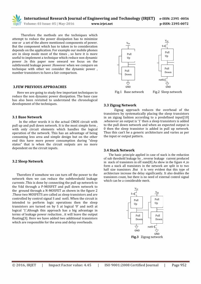
3.1 Base Network In the other words it is the actual CMOS circuit with pull up and pull down network. It is the most simple form , with only circuit elements which handles the logical operation of the network. This has an advantage of being consuming less area and simple design but on the other end this have more power consumption during “sleep states” that is when the circuit outputs are no more dependent on the circuit inputs.
3.2 Sleep Network
Therefore if somehow we can turn off the power to the network then we can reduce the subthreshold leakage currents .This is done by connecting the pull up network to the Vdd through a P-MOSFET and pull down network to the ground through a N-MOSFET as shown in the figure 2 .These two MOSFETS are called as sleep transistors and are controlled by control signal S and notS. When the circuit is intended to perform logic operations then the sleep transistors are turned on by S at logical ‘0’ and notS at logical ‘1’.Altough this approach has a big advantage in terms of leakage power reduction , it will leave the output floating[3]. Here we have added two additional transistors which are responsible for the area and delay overheads.
Fig.1 Base network Fig.2 Sleep network
3.3 Zigzag Network Zigzag approach reduces the overhead of the
transistors by systematically placing the sleep transistors in an zigzag fashion according to a predefined input[10] .whenever an output is ‘1’ then a sleep transistors is added to the pull down network and when an expected output is 0 then the sleep transistor is added in pull up network. Thus this can’t be a generic architecture and varies as per the input or output pattern.
3.4 Stack Network The basic principle applied in case of stack is the reduction
of sub threshold leakage by , reverse leakage current produced in stack of transistors in off state[8].As show in the figure 4 ,to form a stack all transistors in the network are split in to two half size transistors .But it is very evident that this type of architecture increase the delay significantly. It also doubles the transistors count, but there is no need of external control signal which can be a considerable merit.
Fig.3 Zigzag network
Pull
Up
Pull
Up
Pull
Down
Pull
Down
Vdd Vdd
GND GND
S
notS
Pull
Up
Pull
Up
Pull
Down
Pull
Down
Vdd
Vdd
GND GND
S
notS

International Research Journal of Engineering and Technology (IRJET) e-ISSN: 2395 -0056
Volume: 03 Issue: 05 | May-2016 www.irjet.net p-ISSN: 2395-0072
© 2016, IRJET | Impact Factor value: 4.45 | ISO 9001:2008 Certified Journal | Page 953
3.4 Sleepy keeper Network
Sleep keeper approach has been introduced to address the floating output and to retail the output even during the sleep state [2][3]. The basic idea implemented here is a complementary of the basic CMOS network approach. Generally we use a P-MOSFET to connect to the power supply, and N-MOSFET to the ground, as this is the efficient way. However N-MOSFET can also be connected to power supply and P-MOSFET to ground , thus this configuration is used to retain the output , once it has been calculated in the active mode .As shown in the figure 4, two transistors are added parallel to the sleep transistors , these transistors are called keep transistors. Keep transistors are driven by the output as the gate is connected to the output.
Fig.4 Stack network Fig.5 Sleepy keeper
4. ISOLATED SLEEPY KEEPER
The sleepy keeper is good in retaining the output in the sleep state but whenever there are disturbances from the input during the sleep state there occur violent swings in the output.
This type of sleep state can be termed as “Quasi sleep state”. Due to violent swings the separation of output logic levels, ‘VOH-VOL’ becomes too small. When we have this separation too small we can’t read the output and give it as input to other circuit. Figure 6 depicts the fundamentals of noise margin Average noise margin NA is given by equation 3. Rearrangement of the equation clearly shows that to have more noise margin the logical level separation at output ‘VOH-VOL’ should be as much as possible.
NA =(NMH+NML)/2 (3)
= (VOH-VIH+VIL-VOL)/2
= [(VOH-VOL)-(VIH-VIL)]/2
To address the above mentioned two challenges in the sleep state here we introduce Isolated Sleepy Keeper Approach. We tried to isolate the output from the network such that there should no disturbance transfer from base network to the output during the sleep mode.
Fig.6 Noise margin fundamentals
As shown in the figure 7, this is achieved by using the transmission gate .A transmission gate can passes both ‘1’ and ‘0’ in an efficient manner as opposed to the pass transistor which can pass either ‘1’ or ‘0’.This transmission gate is driven by the same control signals which are driving the sleep transistors and that to in the same configuration , that is the PMOSFET is controlled by ‘S’ and NMOSFET by notS. In active mode, S is set to ‘0’ and notS is set to ‘1’ then whatever the outcome, it is transmitted to the output. In sleep mode S is set to ‘1’ and notS is set to ‘0’ thus both transistors of the transmission gate are off and the output is isolated from the base network. As the gates of the keep transistors are connected to the output they retain the last output, which has been calculated just before going in to the sleep mode. As the output is isolated from the input by the transmission gates, the disturbance in the input affects the output to very less extent. Thus even in case of the disturbances we have a good resolution of the output.
Fig.7 Isolated sleepy keeper network
5. EXPERIMENT
To evaluate and compare the Isolated keeper approach which other,1 bit full adder has been taken as the circuit of experiment. The circuit has been implemented with 180nm technology of Taiwan Semiconductor Manufacturing Company (TSMC).Vdd and gate voltage has been taken as 1 V.
W/L=X
W/L=X
W/L=X/2
W/L=X/2
W/L=X/2
W/L=X/2
Pull
Down
Pull
Up
Pull
Up
Vdd Vdd
GND GND
S
notS
Pull
Down
VOH-VOL
VOL
VOH NMH
NML
VIH
VIL
Transmission
gate
Pull
Up
Pull
Down
Input Output
notS
S
notS
S
Vdd Vdd
GND GND
International Research Journal of Engineering and Technology (IRJET) e-ISSN: 2395 -0056
Volume: 03 Issue: 05 | May-2016 www.irjet.net p-ISSN: 2395-0072
© 2016, IRJET | Impact Factor value: 4.45 | ISO 9001:2008 Certified Journal | Page 954
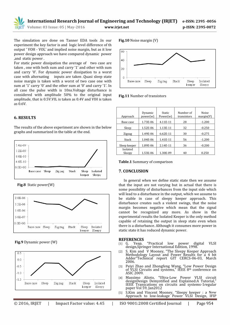
The simulation are done on Tanner EDA tools .In our experiment the key factor is and logic level difference of th output ‘ VOH - VOL’ and implied noise margin, but as it low power design approach we have compared dynamic power ,and static power . For static power dissipation the average of two case are taken , one with both sum and carry ‘1’ and other with sum and carry ‘0’. For dynamic power dissipation to a worst case with alternating inputs are taken .Quasi sleep state noise margin is taken with a worst of two case one with sum at ‘1’ carry ‘0’ and the other sum at ‘0’ and carry ‘1’. In all case the pulse width is 10ns.Voltage disturbance is considered with amplitude 50% to the original input amplitude, that is 0.5V.VIL is taken as 0.4V and VIH is taken as 0.6V.
6. RESULTS The results of the above experiment are shown in the below graphs and summarized in the table at the end.
Fig.8 Static power(W)
Fig.9 Dynamic power (W)
Fig.10 Noise margin (V)
Fig.11 Number of transistors
Approach Dynamic
power(w) Static
Power(w) Number of transistors
Noise
margin(V)
Base case 1.73E-06 4.11E-11 28 -1.200
Sleep 1.52E-06 1.13E-11 32 -0.250
Zigzag 1.49E-06 6.62E-11 30 -0.275
Stack 1.04E-06 1.41E-11 56 -1.200
Sleep keeper 1.89E-06 2.14E-11 36 -0.200 Isolated Sleepy 1.53E-06 1.30E-09 40 0.250
Table.1 Summary of comparison
7. CONCLUSION In general when we define static state then we assume that the input are not varying but in actual that there is some possibility of disturbances from the input side which will lead to a disturbance in the output, which we assume to be stable in case of sleepy keeper approach. This disturbance creates such a violent swings, that the noise margin becomes negative which mean that the signal cannot be recognized any more. As show in the experimental results the Isolated Keeper is the only method capable of retaining the output in sleep state even when there is a disturbance. Although it consumes more power in static state it has reduced dynamic power.
REFERENCES [1] G. Yeap, “Practical low power digital VLSI
design,Springer International Edition, 1998. [2] S. Kim and V Mooney, “The Sleepy Keeper Approach
Methodology Layout and Power Results for a 4 bit Adder”Technical report GIT CERCS-06-03, March 2006.
[3] Peiyi Zhao and Zhongfeng Wang, “Low Power Design of VLSI Circuits and systems,” IEEE 8th conference on ASIC 2009.
[4] Massimo Alioto, “Ultra-Low Power VLSI circuit designDesign Demystified and Explained:A Tutorial,” IEEE Transcations on circuits and systems-1regular paper Vol 59, Jan2012
[5] S.Kim and Vincent Mooney, “Sleepy keeper : a New Approach to low-leakage Power VLSI Design, IFIP

International Research Journal of Engineering and Technology (IRJET) e-ISSN: 2395 -0056
Volume: 03 Issue: 05 | May-2016 www.irjet.net p-ISSN: 2395-0072
© 2016, IRJET | Impact Factor value: 4.45 | ISO 9001:2008 Certified Journal | Page 955
International Conference on Very Large Scale Integration,2006
[6] Tadahiro Kuroda, “Lo-Power ,High-Speed CMOS VLSI Design,” IEEE Proceedings of the International Coneference on computer Design,2002
[7] S. Mutoh et al, “1-V Power Supply High Speed Digital Circuit Technology with Multithreshold-Voltage CMOS” IEEE Journal of Solid state Circuits,august 1995.
[8] J.C Park V.J Mooney and P.Pfeiffenberger,”Sleepy Stack Reduction of Lekage Power,” Proceedings of the
International Workshop on Power and Timming Modeling Optimization and Simulation,September 2004
[9] Predective Technology Model . http://ptm.asu.edu/ [10] K-S Min,H.kawaguchi and T .Sakurai, “Zigzag Super
Cutoff CMOS Block Activation with Self Adaptive Voltage Level Controller : An Alternative to Clock-gatting Scheme in Lekage Dominant Era” IEEE Journal Solid-State Circuits Conference,february 2003