isolated power architecture reference design for
TRANSCRIPT

Digital
Isolator
ISO7741
I2C
Isolator
ISO1541
+ 3.3 V + 5V_iso
+ 3.3 V + 5V_iso
LDO TPS7A1633+3,3 V
Fly-Buck
Converter
LM5017
TPS55010
LDO
TPS7A4700R
LDO
TPS7A3001
LDO
TPS7A1650
LP2985
TVS0500
+5 VTVS3300
+24 V
SPI Interface
I2C Interface
NON-ISOLATED
Voltage (24 V or
5 V input)
+
SPI, I2C
Interface Connector
SPI Interface
I2C Interface
ISOLATED
SPI, I2C
Interface
Connector
+15V_iso
-15V_iso
+15V_iso
Isolated
GND
DGND Isolated GND
DGND Isolated GND3 LEDs: +15 V, -15 V,
and +5 V
1TIDU562B–October 2014–Revised October 2019Submit Documentation Feedback
Copyright © 2014–2019, Texas Instruments Incorporated
Isolated Power Architecture Reference Design for Communication andAnalog Input/Output Modules
Design Guide: TIDA-00300Isolated Power Architecture Reference Design forCommunication and Analog Input/Output Modules
DescriptionThis reference design includes multiple approaches forgeneration of isolated power supplies for differentprotection relay modules. Isolated supply for analoginput, binary input, and communication modules isgenerated using an isolated DC/DC converter withoutput headroom for connecting to an LDO andconfigurable output. Additionally, this designshowcases LDOs for regulating the supplies,monitoring the DC voltage status using a voltagedetector, and input or output overload protection usingload switches.
Resources
TIDA-00300 Design FolderUCC12050, TPS782, TPS760, TLV713 Product FolderSN6505B, SN6501, TPS709, TPS61220 Product FolderISOW7841, TPS763, TPS22944, TLV3012 Product FolderREF3025, LM5017, TPS7A47, TPS7A16 Product FolderISO7741, ISO1541, TPS55010, TVS3300 Product FolderDCH010515D, DCH010505S, REF3425 Product Folder
Search Our E2E™ support forums
Features• Multiple approaches for generation of isolated
power supplies for analog input, binary input, andcommunication module using transformer driver,power module, or isolated DC/DC
• Use of isolated DC/DC converter simplifies systemdesign, provides flexibility in configuring the output,and improves reliability
• Multiple approaches for generation of isolatedpower supplies for analog input or output moduleincluding split-rail power supplies using a DC/DCconverter and LDOs, Fly-Buck™ converters, split-rail DC/DC, and LDOs
• Synchronous SPI interface using digital isolator andI2C interface using digital isolators with bidirectionalSDA and unidirectional SCL
• The boards are tested for the EMI pre-compliancerequirement and the EMC pre-compliance byinterfacing to the TIDA-00227 design
Applications• AC analog input module• Communication module• Multifunction relay
An IMPORTANT NOTICE at the end of this TI reference design addresses authorized use, intellectual property matters and otherimportant disclaimers and information.

Resources (Continued) www.ti.com
2 TIDU562B–October 2014–Revised October 2019Submit Documentation Feedback
Copyright © 2014–2019, Texas Instruments Incorporated
Isolated Power Architecture Reference Design for Communication andAnalog Input/Output Modules
1 Resources (Continued)
TLV742P, TLV704, TPS22960, SN74LVC1G14 Product FolderTPS62821, DCR010505, LP2985-N , TPS3897 Product FolderTPS3895, TPS7A39, DCP010505B, TPS7A3001-EP Product FolderLM5160, TPS65130, LM27762, REF3025 Product FolderOPA2376, REF5025, LM4040, TPS22917 Product Folder
2 System Description
2.1 Need for IsolationIndustrial electronic equipment commonly uses galvanic isolators to protect systems and users frompotentially hazardous voltages. Industrial equipment must operate reliably in the harshest environments,where strong electromagnetic fields, surges, fast transients, and high noise floors are normal. Thisenvironment presents challenges for designing reliable isolation circuits that deliver error-free operationover long equipment lifetimes. Over many decades, optocouplers have been the default signal isolationdevice, but recent breakthroughs in silicon isolation technology have spawned smaller, faster, and morereliable and cost-effective solutions that have already begun supplanting optocouplers in many endapplications.
Benefits of Digital Isolators
• Higher integration: smaller size and lower cost per channel on multi-channel versions• Higher performance: faster, tighter timing, and substantially lower power• Longer service life: no wear-out mechanisms as in optocouplers• Higher reliability: operating parameters remain stable over VDD, temperature, and device age• High CMTI: an isolation signal path that is fully differential and a high receiver selectivity for CMTI
greater than 15 kV/μs• Low EMI• High electric-field immunity: >20 V/m, as measured by independent laboratories• Industry-leading ESD tolerance: 3-kV HBM on all devices• Lower external bill-of-materials• Easy to use: single-chip, complete isolation solution
2.2 I/Os in Smart GridA number of IEDs or protection relays are used in smart grid and protection systems. These IEDs andprotection relays have following I/Os:• RTD inputs• DC voltage transducers (0 to 10 V)• DC current transducers (4 to 20 mA)• Binary inputs and outputs
The number of inputs vary depending on the application. If the application requires more I/Os andprotection relay has a limited number of I/Os, external expansion modules are used to increase thenumber of I/Os.
Isolation In Smart Grid
The previously-described external expansion modules are standalone devices that sense any of the listedinputs and provide the information to the IED and protection relay through RS-485 communication. Theseexpansion devices need the following isolation:• Communication• Power supply, as they are operated from an auxiliary DC input
www.ti.com System Description
3TIDU562B–October 2014–Revised October 2019Submit Documentation Feedback
Copyright © 2014–2019, Texas Instruments Incorporated
Isolated Power Architecture Reference Design for Communication andAnalog Input/Output Modules
• Isolation for the previously mentioned I/Os
The required number of I/Os also varies with application and vary from 8 to 16. To control each I/O, anindividual isolated channel is required. Alternative to isolating individual channel is to use serialcommunication with expansion options on the non-isolated side. I2C, a 2-wire communication technology,is commonly used for such applications. Many I2C expanders are available as part of the TI expanderportfolio for this kind of application.
I2C is a simple, low-bandwidth, short-distance protocol. Most available I2C devices operate at speeds upto 400 Kbps, with some venturing up into the low megahertz range. I2C can easily link multiple devicestogether because it has a built-in addressing scheme.
I2C advantages are:• Requires only two bus lines (SDA and SCL)• No strict baud rate requirements, the master generates a bus clock• Simple master/slave relationships between all components• Each device connected to the bus is software-addressable by a unique address• A true multi-master bus providing arbitration and collision detection
Analog inputs are interfaced with analog-to-digital converters (ADCs), and analog outputs are generatedthrough digital-to-analog converters (DACs). Most of the ADCs and DACs are available with SPI.
SPIs can daisy chain multiple devices. An advantage of daisy chaining is the reduced requirement fornumber of chip selects. Many SPI-based ADCs and DACs are available as part of TI's portfolio.
In most applications, these modules work on auxiliary supply. The available auxiliary input for smart gridapplications is 24 V. For safety reasons, isolate the auxiliary modules. To generate the required supplyvoltages, a switching regulator is used. When digital isolators are used to isolate SPI and I2C aspreviously described, an isolated and a non-isolated supply are required to function.
To generate both the isolated and non-isolated supply, a synchronous buck regulator with Fly-Bucktopology can be used. The Fly-Buck topology can generated both isolated and non-isolated voltages withgood regulation.
The ADC and DAC require different supply voltages to operate. Most common supply voltages used are±15 V, 5 V, 3.3 V. The output of the Fly-Buck is an unregulated output. LDOs are used to regulatevoltages to the required levels.
An isolated buck converter (Fly-Buck) uses a synchronous buck converter with coupled inductor windingsto create isolated outputs. Isolated converters utilizing Fly-Buck topology use a smaller transformer for anequivalent power transfer as the transformer primary and secondary turns ratios are better matched. Anoptocoupler or auxiliary winding is not needed as the secondary output closely tracks the primary outputvoltage, resulting in a smaller solution size and cost.

System Description www.ti.com
4 TIDU562B–October 2014–Revised October 2019Submit Documentation Feedback
Copyright © 2014–2019, Texas Instruments Incorporated
Isolated Power Architecture Reference Design for Communication andAnalog Input/Output Modules
2.3 Isolation TypesThe signal isolation can be achieved by:• Optical coupling: The transmission of light across a transparent nonconductive barrier, such as an air
gap, to achieve isolation. The main benefits of optical coupling (optocoupling) are that light is inherentlyimmune to external electric or magnetic fields, and optical coupling allows for transfer of steady-stateinformation. The disadvantages of optocouplers include speed limitations, power dissipation, and thedegradation of the LED. The advantage of inductive coupling is the possible difference in common-mode and differential transfer characteristics
• Inductive coupling: Uses a changing magnetic field between two coils to communicate across anisolation barrier. The most common example is the transformer where the strength of the magneticfield depends on the coil structure (number of turns/unit length) of the primary and secondary windings,the permittivity of the magnetic core, and the current magnitude.
• Capacitive coupling: Uses a changing electric field to transmit information across the isolation barrier.The material between the capacitor plates is a dielectric insulator and forms the isolation barrier. Theplate size, the distance between the plates, and the dielectric material determine the electricalproperties. The benefits of using a capacitive isolation barrier are efficiency, in both size and energytransfer, and immunity to magnetic fields.
2.4 Digital IsolatorDigital isolators use innovative circuitry to isolate standard digital signals at signaling rates of DC to over100 Mbps. The TI family of isolators use capacitive coupling. The capacitive coupling solution uses provenand cost-effective manufacturing processes and provides an inherent immunity to magnetic fields.
Device SelectionSystem performance requirements have the most impact on the selection of an isolation device. Otherconsiderations include space constraints and cost.
Data Rate RequirementsSystem data rate requirements are likely to be the single most important parameter for device selection. Ifa system uses high data rates, such as the high speed PROFIBUS protocol, the minimum data rate speedrequirement of 9.6 Mbps narrows the device selection to the high performance products available.Conversely, if the RS-485 network runs at much lower data rate speeds, the possible device selectionoptions widens.
Device costs typically rise in proportion to data rate performance. Therefore, a designer must take carenot to specify a device with more performance than is required. However, low performance deviceselection can make future system performance upgrades more costly and involved, because all devicesnot compatible with upgraded system data speeds require replacement.
Space RequirementsSpace constraints are a second area of concern that can also limit a designer’s choices. Maximumdimension requirements are a concern for virtually all applications. However, some implementations canbe severely space-limited. Fortunately, there are solutions for these situations.
Cost RequirementsCost constraints and concerns are a reality in virtually all system design work, and therefore must beconsidered. Cost considerations can have an effect on the design choices for a system. As notedpreviously, isolator device cost rises in proportion with data rate performance. Specifying a device withonly the system performance required can reduce costs. Other cost issues include a consideration of thenumber of devices used.
www.ti.com System Description
5TIDU562B–October 2014–Revised October 2019Submit Documentation Feedback
Copyright © 2014–2019, Texas Instruments Incorporated
Isolated Power Architecture Reference Design for Communication andAnalog Input/Output Modules
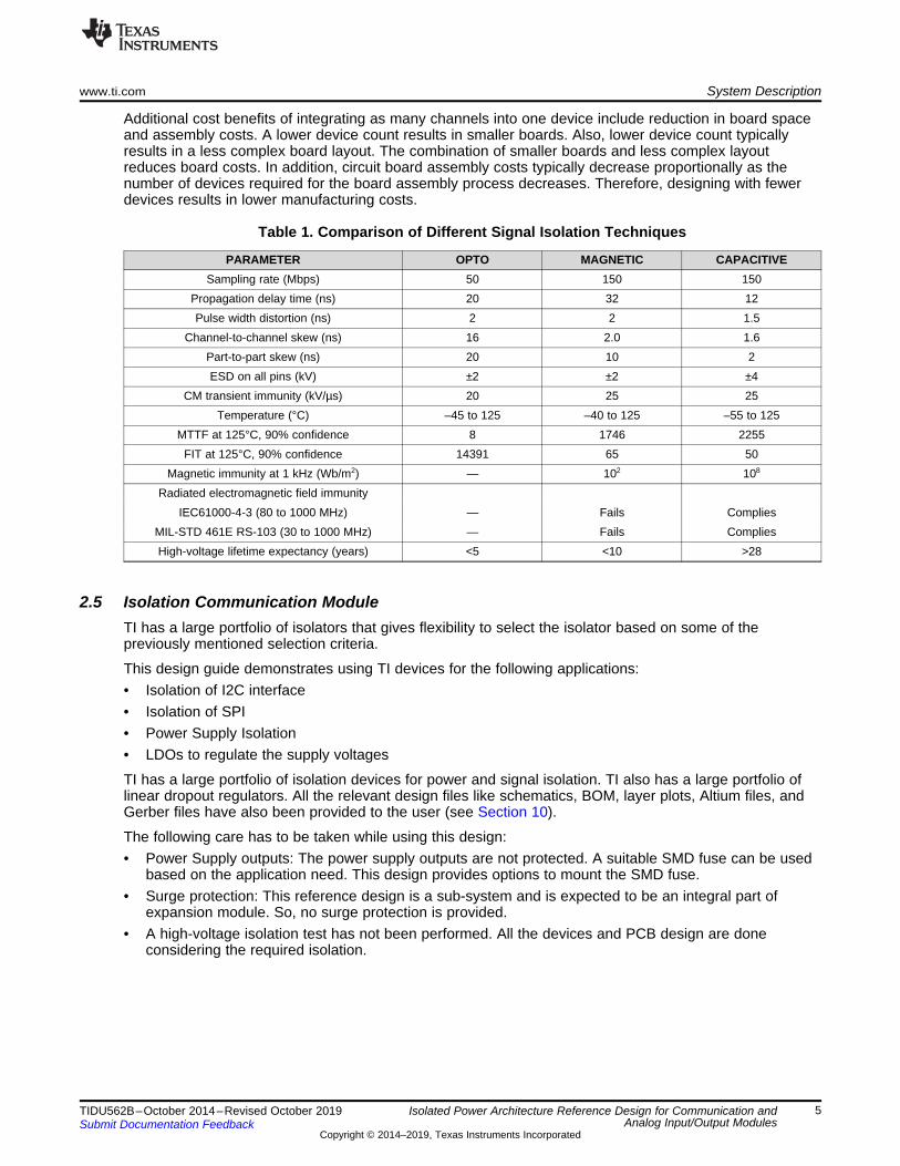
Additional cost benefits of integrating as many channels into one device include reduction in board spaceand assembly costs. A lower device count results in smaller boards. Also, lower device count typicallyresults in a less complex board layout. The combination of smaller boards and less complex layoutreduces board costs. In addition, circuit board assembly costs typically decrease proportionally as thenumber of devices required for the board assembly process decreases. Therefore, designing with fewerdevices results in lower manufacturing costs.
Table 1. Comparison of Different Signal Isolation Techniques
PARAMETER OPTO MAGNETIC CAPACITIVESampling rate (Mbps) 50 150 150
Propagation delay time (ns) 20 32 12Pulse width distortion (ns) 2 2 1.5
Channel-to-channel skew (ns) 16 2.0 1.6Part-to-part skew (ns) 20 10 2ESD on all pins (kV) ±2 ±2 ±4
CM transient immunity (kV/µs) 20 25 25Temperature (°C) –45 to 125 –40 to 125 –55 to 125
MTTF at 125°C, 90% confidence 8 1746 2255FIT at 125°C, 90% confidence 14391 65 50
Magnetic immunity at 1 kHz (Wb/m2) — 102 108
Radiated electromagnetic field immunityIEC61000-4-3 (80 to 1000 MHz) — Fails Complies
MIL-STD 461E RS-103 (30 to 1000 MHz) — Fails CompliesHigh-voltage lifetime expectancy (years) <5 <10 >28
2.5 Isolation Communication ModuleTI has a large portfolio of isolators that gives flexibility to select the isolator based on some of thepreviously mentioned selection criteria.
This design guide demonstrates using TI devices for the following applications:• Isolation of I2C interface• Isolation of SPI• Power Supply Isolation• LDOs to regulate the supply voltages
TI has a large portfolio of isolation devices for power and signal isolation. TI also has a large portfolio oflinear dropout regulators. All the relevant design files like schematics, BOM, layer plots, Altium files, andGerber files have also been provided to the user (see Section 10).
The following care has to be taken while using this design:• Power Supply outputs: The power supply outputs are not protected. A suitable SMD fuse can be used
based on the application need. This design provides options to mount the SMD fuse.• Surge protection: This reference design is a sub-system and is expected to be an integral part of
expansion module. So, no surge protection is provided.• A high-voltage isolation test has not been performed. All the devices and PCB design are done
considering the required isolation.

System Description www.ti.com
6 TIDU562B–October 2014–Revised October 2019Submit Documentation Feedback
Copyright © 2014–2019, Texas Instruments Incorporated
Isolated Power Architecture Reference Design for Communication andAnalog Input/Output Modules
2.6 Isolated DC-DC Converter UCC12050 AdvantagesSome of the advantages of using an isolated DC/DC converter include:• Fully integrated high-efficiency isolated DC-DC converter• Regulated 5.0-V or 3.3-V output with selectable 400-mV headroom voltage to power an LDO• Extended ambient temperature range: –40ºC to +125ºC• Short circuit tolerant and provides thermal shutdown• Extended ambient temperature range: –40ºC to +125ºC
The UCC12050 provides extra features such as an enable pin, synchronization of switching frequencyamong multiple devices, and selection of isolated output voltages.

www.ti.com Design Features
7TIDU562B–October 2014–Revised October 2019Submit Documentation Feedback
Copyright © 2014–2019, Texas Instruments Incorporated
Isolated Power Architecture Reference Design for Communication andAnalog Input/Output Modules
3 Design FeaturesThe primary objective is to create a reference design platform to showcase different approaches togeneration of isolated power-supply rails including a split-rail supply required for communication, analoginput, and analog output modules from 24-V or 5-V DC input using a DC/DC converter with integratedFET, split-rail DC/DC converter, isolated power module, and transformer driver. The design additionallyfeatures generation of a stable reference using low drift references, diagnostics of input voltage,synchronous communication using digital isolators, and input protection using load switches. Table 2 liststhe typical requirements:
Table 2. System Specifications for TIDA-00300
PART NUMBER NAME DESCRIPTION1 SPI interface 4-wire , up to 4Mbps2 I2C interface Bidirectional data , unidirectional clock , up to 100 Kbps
3 Fly-Buck converterOutput voltages
Isolated: > 18 V, < –18 V, > 7 VNon-isolated > 9 V
4 Input voltage, connection 24-V DC nominal input, screw-type terminal5 Regulators (LDOs) Isolated: 15 V, –15 V, 5 V; Non-isolated: 3.3 V
6 Protection Undervoltage lockout for Fly-Buck converterSupply input reversal
7 Host input connection 8-pin screw type terminal block
8 Output connection 8-pin screw type terminal block for signal4-pin screw type terminal block for power
9 Indication LED indications for 15-V, –15-V, and 5-V isolated powersupplies
10 Generation of isolated supplies using DC/DCpower module ±15 V , 6 V, 5 V , 3.3 V
11 Generation of isolated supplies usingtransformer driver and LDO ±13 V , ±12 V, 6 V, 5 V, 3.3 V
12 Generation of isolated supplies using isolatedDC/DC with configurable outputs 5.4 V, 5 V , 3.7 V, 3.3 V
13 Generation of isolated supplies using digitalisolator with integrated power 5.4 V, 5 V , 3.3 V
14 Generation of split-rail supplies using isolatedDC/DC converter with integrated FETS ±15 V, 5 V
15 Generation of isolated split rail using wideinput synchronous buck, Fly-Buck converter ±18 V, ±15 V, 5 V
16 Generation of stable reference output usingseries or shunt reference 2.5 V

TI Device Mapping to Reference Design Functionalities www.ti.com
8 TIDU562B–October 2014–Revised October 2019Submit Documentation Feedback
Copyright © 2014–2019, Texas Instruments Incorporated
Isolated Power Architecture Reference Design for Communication andAnalog Input/Output Modules
4 TI Device Mapping to Reference Design FunctionalitiesThis section provides details of device mapping to functionalities for the following boards:• Isolated power supply for communication module• Isolated power supply for analog IO module• Isolated synchronous communication with split-rail power supplies
4.1 Isolated Power Supply for Communication ModuleTable 3 provides details of the TI devices and functionalities implemented in this reference design forgenerating isolated power supplies for the communication module.
Table 3. Details of Functions and Devices Used for Implementing Power Supplies for CommunicationModule
FUNCTION DEVICES DESCRIPTIONIsolated 5-V and 3.3-V supplygeneration using power module
DCR010505P, DCP010505BP,LP2985AIM5-3.3, TPS78233
Generation of isolated, regulated and unregulated DC supplyusing isolated DC/DC converter modules and LDOs
Isolated 5-V, 3.3-V, and ±12-Vsupply generation usingtransformer driver
SN6505B, SN6501, TPS70933,TPS76050, TPS7A3901
Generation of isolated supply including split-rail power supply foranalog input module using transformer driver and LDOs
Isolated 5.4-V, 5-V, and 3.3-Vsupply using digital isolator withintegrated power
ISOW7841, TPS22944, TPS61220,TPS76350, TPS62821
Generation of isolated using digital isolator with integratedpower, DC/DC converter to boost the output and LDOs toregulate the output
Generation of regulated DCsupplies with diagnostics
UCC12050, SN74LVC1G14,SN74LVC1G14, CSD17571Q2,
TPS22960, TLV74233, TLV70450,TLV71333, TPS3897, SN74LVC1G17
Generation of isolated power supplies with configurable outputand regulating the output using LDOs including 5-V and 3.3-Voutput with input overload protection, voltage level detection andvoltage status indication
4.2 Wide Input Isolated Power Supply for Analog IO ModulesTable 4 provides details of the TI devices and functionalities implemented in this reference design forgenerating isolated power supplies for analog IO modules.
Table 4. Details of Functions and Devices Used for Implementing Power Supply for Analog IO Modules
FUNCTION DEVICES DESCRIPTION
Generation of isolated 5 V and±15 V using DC/DC, split-railDC/DC, and power module
TVS3300, LM5160, TVS0500,TPS22917, SN6505B, TPS2400,
DCH010515D, DCH010505S,TPS65130
Generation of split-rail power supply for analog input and analogoutput from 24-V or 5-V DC input with input protection
Generation of regulated 3.3 V, ±5V and ±12 V using LDOs
LM27762, TPS7A3901, TLV70433,TVS1400
Generation of regulated split-rail supplies from unregulated split-rail supplies
Generation of stable reference REF5025, REF3025A, REF3425,OPA2376, LM4040AIM3-2.5 Generation of stable reference using series or shunt reference

www.ti.com TI Device Mapping to Reference Design Functionalities
9TIDU562B–October 2014–Revised October 2019Submit Documentation Feedback
Copyright © 2014–2019, Texas Instruments Incorporated
Isolated Power Architecture Reference Design for Communication andAnalog Input/Output Modules
4.3 Isolated Synchronous Communication With Split-Rail Power SuppliesTable 5 provides details of the TI devices and functionalities implemented in this reference design forgenerating isolated power supplies for analog IO module and isolated synchronous communication.
Table 5. Details of Functions and Devices Used for Implementing Power Supply and SynchronousCommunication
FUNCTION DEVICES DESCRIPTION
Generation of 5 V and ±15 Vfrom 24-V input using DC/DC
TVS3300, LM5017, TPS70933,TPS7A4700, TPS7A3001,
TPS7A1650
Generation of split-rail power supply output from 12- or 24-Vinput using isolated DC/DC converter with integrated switch
Generation of 5 V and ±15 Vfrom 5-V input using DC/DC TPS55010, TVS0500, LP2985- Generation of split-rail power supply output from a 5-V input
using isolated DC/DC converter with integrated switch
Isolated SPI interface ISO7741, ISO7141 Digital isolator with basic or reinforced isolation to implementSPI with varying speed
Isolated I2C interface ISO1541D Digital isolators to implement I2C interface with varying speed
5 System OverviewSome of the key requirements for designing the isolated power architecture for protection relay modulesinclude:1. Generation of isolated 5 V or 3.3 V with output headroom allowing usage of LDOs for applications in
an analog input module or communication module2. Generation of the required supply rails (5 V to ±14 V, ±14 V to ±12 V, 5 V to ±5 V for analog IO and 5
V and 3.3 V for communication) with high efficiency and scalable load current using 5-V, 12-V, or 24-Vinput
3. Operation of the supply over wide range for applications using external auxiliary supply4. Generation of isolated power supplies with high efficiency5. Generation of stable reference (Series or Shunt) with buffer and low temperature drift6. Isolation of SPI signals with varying speed and low current consumption7. Isolation of I2C interface signals with varying speed8. Generation of isolated power supplies with low EMI for ease of design9. Diagnostics including LEDs and voltage detection
The TIDA-00300 reference design provides solutions to the previous requirements and also solves someof the design challenges associated with the design of isolated power architecture for protection relaymodules.

5 V
Gnd
5 V
Gnd
TPS22944
TLV3012
5 V
Gnd
5 V
3.3 V
5.4 V5 V
Digital isolator with integrated power
±13 V
5 V
GND ±12 V
Transformer driver based isolated power
DCR010505 5 V
5 V
GND
3.3 V
DCP01050BP3.3 V
Miniature, 1 W Isolated Regulated DC/DC Converters
TPS78233
LP2985-3.3
TPS7A39SN6505
6 V5 V
GND 3.3 VTPS7A39SN6505
6 V5 V
GND 5 VTPS7A39SN6505
ISOW7841 TPS61220 TPS76350
TPS62821
TPS3897
TLV70450
TPS62821
TPS3897
TLV70450
TPS62821
SN74LVC1G17
SN74LVC1G17
Iso_Supply_OK
Iso_Supply_OK
5 V
3.3 V
5 V
3.3 V
UCC12050
SN74LVC1G14
CSD17585F5T
UCC12050
SYNC
SYNC_OK
TPS22960
(Part B)
TPS22960
(Part A)
Stitched Cap
Routing
Isolated DC-DC Converter
5.4 V
5.4 V
LED Buffer
System Overview www.ti.com
10 TIDU562B–October 2014–Revised October 2019Submit Documentation Feedback
Copyright © 2014–2019, Texas Instruments Incorporated
Isolated Power Architecture Reference Design for Communication andAnalog Input/Output Modules
5.1 Block DiagramBlock diagram for the boards used for generating power supplies used for isolated communication andisolated IO modules are discussed in this section.
5.1.1 Isolated Power Supply for Communication ModuleFigure 1 shows multiple approaches to generation of isolated power supply for low-speed wiredcommunication modules.
Figure 1. Isolated Power Supply Architecture for Communication Modules

TVS0500
TVS0500TVS0500
TVS0500
TPS2400
5 VTPS22917
DCH010505S
DCH010515D
5 V
±15 V
Isolated DC-DC Modules
SN6505B_Iso
LM5160_Iso
Isolated DC-DC Converter
TLV70433
TPS65130 TPS7A39
LM27761±5 V
DUAL Supply LDOs
±15 V
TVS1800
LM4040
REF3025
REF3425
REF5025
OPA2376
Reference with Buffer
Input Voltage
OK
24 V
AFE Isolated Power Supply
2.5 V
2.5 V
www.ti.com System Overview
11TIDU562B–October 2014–Revised October 2019Submit Documentation Feedback
Copyright © 2014–2019, Texas Instruments Incorporated
Isolated Power Architecture Reference Design for Communication andAnalog Input/Output Modules
5.1.1.1 Generation of Isolated 5-V, 5.4-V, 3.3-V, or 3.7-V Supply Using Isolated DC/DC With Protectionand Diagnostics
This design has the following functionality:• Configuration of output voltage using output select pin and resistors• Generation of regulated 5-V and 3.3-V supplies• Protection of 5-V input using a load switch• Voltage detector to indicate the isolated supply status
5.1.1.2 Isolated 5-V and 3.3-V Supply Generation Using Power ModuleThis design has the following functionality:• Generation of 5-V DC power supply from 5-V input using an unregulated power module• Generation of 5-V DC power supply from 5-V input using a regulated power module• Generation of regulated 3.3-V output using LDO
5.1.1.3 Isolated 5-V, 3.3-V and ±12-V Supply Generation Using Transformer DriverThis design has the following functionality:• Generation of isolated 3.3 V or 5 V from 5-V input using a transformer driver• Generation of split-rail ±12-V supply from 5-V input using a transformer driver
5.1.1.4 Isolated 5.4-V, 5-V and 3.3-V Supply Using Digital Isolator With Integrated PowerThis design has the following functionality:• Generation of isolated 5 V from 5-V input using digital isolators with integrated power• Generation of isolated 5.4 V, regulated 5 V, 3.3 V from 5 V
5.1.2 Wide Input Isolated Power Supply for Analog IO ModulesFigure 2 shows multiple approaches to generation of isolated power supply for analog input/outputmodules.
Figure 2. Wide Input Isolated Power Supply Architecture for Analog IO Modules

Digital
Isolator
ISO7741
I2C
Isolator
ISO1541
+ 3.3 V + 5V_iso
+ 3.3 V + 5V_iso
LDO TPS7A1633+3,3 V
Fly-Buck
Converter
LM5017
TPS55010
LDO
TPS7A4700R
LDO
TPS7A3001
LDO
TPS7A1650
LP2985
TVS0500
+5 VTVS3300
+24 V
SPI Interface
I2C Interface
NON-ISOLATED
Voltage (24 V or
5 V input)
+
SPI, I2C
Interface Connector
SPI Interface
I2C Interface
ISOLATED
SPI, I2C
Interface
Connector
+15V_iso
-15V_iso
+15V_iso
Isolated
GND
DGND Isolated GND
DGND Isolated GND3 LEDs: +15 V, -15 V,
and +5 V
System Overview www.ti.com
12 TIDU562B–October 2014–Revised October 2019Submit Documentation Feedback
Copyright © 2014–2019, Texas Instruments Incorporated
Isolated Power Architecture Reference Design for Communication andAnalog Input/Output Modules
5.1.2.1 Generation of Isolated 5 V and ±15 V With ProtectionThis design has the following functionality:• Generation of isolated split-rail supplies using DC/DC converter with integrated switch from 24-V input• Generation of isolated split-rail supplies using isolated power module from 5-V input• Input protection against overload using a load switch• Input protection against transients using a flat clamp TVS
5.1.2.2 Generation of Regulated 3.3-V, ±5-V and ±12-V Supplies Using LDOsThis design has the following functionality:• Generation of regulated split-rail supply using a dual LDO• Generation of 5 V and 3.3 V using LDOs
5.1.2.3 Generation of Stable ReferenceThis design has the following functionality:• Generation of stable reference using shunt reference with buffer• Generation of stable reference using series reference with buffer
5.1.3 Isolated Synchronous Communication With Split-Rail Fly-Buck™ PowerFigure 3 shows multiple approaches to the generation of isolated power supply for synchronouscommunication and analog IO modules with protection.
Figure 3. Isolated Synchronous Communication With Split-Rail Fly-Buck™ Power

www.ti.com System Overview
13TIDU562B–October 2014–Revised October 2019Submit Documentation Feedback
Copyright © 2014–2019, Texas Instruments Incorporated
Isolated Power Architecture Reference Design for Communication andAnalog Input/Output Modules
5.1.3.1 Generation of 5 V and ±15 V from 24 VThis design showcases the following:• Generation of split-rail supply from 24-V input using a DC/DC converter• Generation of regulated split-rail supply using LDOs• Input transient protection using a flat clamp TVS
5.1.3.2 Generation of 5 V and ±15 V from 5-V inputThis design has the following functionality:• Generation of split-rail supply from 5-V input using a DC/DC converter• Generation of 5 V using LDO• Input transient protection using flat clamp
5.1.3.3 Isolated Synchronous InterfaceThis design has the following functionality:• SPI using digital isolator• I2C interface using digital isolators
5.2 Highlighted ProductsThis section provides details of some of the focus TI products used in this reference design for generationof required power supplies for protection relay modules.
5.2.1 Isolated Power Supply for Communication ModuleThis section provides details of the devices used to generate the required isolated power supplies for thecommunication module:
5.2.1.1 Generation of Isolated 5-V, 5.4-V, 3.3-V, or 3.7-V Supply Using Isolated DC/DC With Protectionand Diagnostics
This design has the following functionality:• UCC12050, 500-mW, high-efficiency, 5-kVRMS isolated DC-DC converter• TPS22960, 5.5-V, 0.5-A, 435-mΩ, 2-channel load switch with quick output discharge• TLV74233, 200-mA small-size low-dropout (LDO) linear voltage regulator• TLV70450, 24-V input voltage, 150-mA, ultra-low IQ low-dropout (LDO) regulators• TLV713, 150-mA low-dropout (LDO) regulator with fold-back current limit for portable devices• TPS3897, single-channel ultra-small adjustable supervisory circuit with active-high, open-drain output• SN74LVC1G14, single Schmitt-trigger inverter• SN74LVC1G17, single Schmitt-trigger buffer• CSD17571Q2, 30-V N-channel NexFET™ power MOSFETs
5.2.1.2 Isolated 5-V and 3.3-V Supply Generation Using Power ModuleThis design has the following functionality:• DCR010505P, miniature, 1-W isolated unregulated DC/DC converters• DCP010505BP, miniature, 1-W isolated unregulated DC/DC converters in a PDIP package• LP2985AIM5-3.3, 150-mA low-noise low-dropout regulator with shutdown• TPS78233, 3.3-V, 150-mA, ultra-low quiescent current (500 nA) low-dropout linear regulator
System Overview www.ti.com
14 TIDU562B–October 2014–Revised October 2019Submit Documentation Feedback
Copyright © 2014–2019, Texas Instruments Incorporated
Isolated Power Architecture Reference Design for Communication andAnalog Input/Output Modules
5.2.1.3 Isolated 5-V, 3.3-V and ±12-V Supply Generation Using Transformer DriverThis design has the following functionality:• SN6505B, low-noise 1-A, 420-kHz transformer driver for isolated power supplies• SN6501, low-noise, 350-mA, 410-kHz transformer driver for isolated power supplies• TPS70933, 3.3-V, 150-mA 30-V ultra-low IQ wide-input low-dropout (LDO) regulator with reverse
current protection• TPS76050, 5-V output, 16-V, 50-mA, low IQ, low-dropout linear regulator• TPS7A3901, dual, 150-mA, wide-VIN, positive and negative low-dropout (LDO) voltage regulator
www.ti.com System Overview
15TIDU562B–October 2014–Revised October 2019Submit Documentation Feedback
Copyright © 2014–2019, Texas Instruments Incorporated
Isolated Power Architecture Reference Design for Communication andAnalog Input/Output Modules
5.2.1.4 Isolated 5.4-V, 5-V, and 3.3-V Supply Using Digital Isolator With Integrated PowerThis design has the following functionality:• TPS22944, 5.5-V, 0.2-A, 500-mΩ, 100-mA current-limit load switch• ISOW7841, high-efficiency, low-emissions, reinforced digital isolator with integrated power• TPS61220, low input voltage, 0.7-V boost converter with 5.5-μA quiescent current• TPS76350, low IQ, 150-mA, low-dropout linear regulators• TPS62821, 1-A step-down converter with 1% accuracy
5.2.2 Wide Input Isolated Power Supply for Analog IO ModulesThis section provides details of the devices and configurations used to generate the required isolatedpower supplies for an analog IO module.
5.2.2.1 Generation of Isolated 5-V and ±15-V With ProtectionThis design has the following functionality:• LM5160, wide input 65-V, 2-A synchronous buck or Fly-Buck converter• TPS22917, ultra-low leakage, 5.5-V, 2-A, 80-mΩ on-resistance load switch• SN6505B, low-noise 1-A, 420-kHz transformer driver for isolated power supplies• TPS2400, 5.5-V overvoltage protection controller with 100-V input transient protection• DCH010515D, miniature, 1-W, 3-kV DC isolated DC/DC converters with dual output• DCH010505S, miniature, 1-W, 3-kV DC isolated DC/DC converters• TPS65130, split-rail converter with dual, positive and negative outputs (300 mA typ)• TPS65130, split-rail converter with dual, positive and negative outputs (300 mA typ)• TVS0500, 5-V flat-clamp surge protection device
5.2.2.2 Generation of Regulated 3.3-V, ±5-V and ±12-V Supplies Using LDOsThis design has the following functionality:• TPS7A3901, dual, 150-mA, wide-Vin, positive and negative low-dropout (LDO) voltage regulator• LM27762, low-noise positive- and negative-output charge pump with integrated LDO• TLV70433, 24-V input voltage, 150-mA, ultra-low IQ low-dropout (LDO) regulators• TVS1400, 14-V flat-clamp surge protection device

System Overview www.ti.com
16 TIDU562B–October 2014–Revised October 2019Submit Documentation Feedback
Copyright © 2014–2019, Texas Instruments Incorporated
Isolated Power Architecture Reference Design for Communication andAnalog Input/Output Modules
5.2.2.3 Generation of Stable ReferenceThis design has the following functionality:• REF5025, 3-µVpp/V, noise, 3 ppm/°C drift precision series voltage reference• REF3025, 2.5-V, 50-ppm/°C, 50-µA in SOT23-3 series (Bandgap) voltage reference• REF3425, 2.5-V, low-drift low-power small-footprint series voltage reference• LM4040AIM3-2.5, precision micropower shunt voltage reference• OPA2376, precision, low noise, low quiescent current operational amplifier
5.2.3 Isolated Synchronous Communication With Split-Rail Fly-Buck™ PowerThis section provides details of the devices used to generate the required isolated power supplies foranalog IO module and digital isolators used for isolated synchronous communication.
5.2.3.1 Generation of 5 V and ±15 V from 24-V inputThis design has the following functionality:• LM5017, 7.5 V–100 V wide VIN, 600-mA constant on-time synchronous buck• TPS7A4700, 36-V, 1-A, 4.17-μVRMS, RF low-dropout (LDO) voltage regulator• TPS7A3001, VIN, –3 V to –36 V, –200 mA, ultra-low noise, high-PSRR, low-dropout (LDO) linear
regulator• TPS7A1650, 60-V, 5-µA IQ, 100-mA, low-dropout (LDO) voltage regulator with enable and power good• TPS70933, 150-mA 30-V ultra-low IQ wide-input low-dropout (LDO) regulator with reverse current
protection• TVS3300, 33-V flat-clamp surge protection device
5.2.3.2 Generation of 5 V and ±15 V from 5-V inputThis design showcases the following functionality:• TPS55010, 2.95-V to 6-V input, 2-W, isolated DC/DC converter with integrated FETS• LP2985-50, 150-mA low-noise low-dropout regulator with shutdown• TVS0500, 5-V flat-clamp surge protection device
5.2.3.3 Isolated Synchronous InterfaceThis design has the following functionality:• ISO7741, high-speed, low-power, robust EMC quad-channel digital isolator• ISO7141, 4242-VPK small-footprint and low-power 3/1 quad-channel digital isolator with noise filter• ISO1541D, 2.5-kVRMS isolated unidirectional clock, bidirectional I2C isolators
5.2.4 System DesignThe design is split into multiple boards as described in this section:1. Isolated power supply for communication module2. Wide input isolated power supply for analog IO modules3. Isolated synchronous communication with split-rail Fly-Buck power
5.2.4.1 Isolated Power Supply for Communication ModuleThis section provides details of the devices used to generate the required power supplies for isolatedcommunication module.

www.ti.com System Overview
17TIDU562B–October 2014–Revised October 2019Submit Documentation Feedback
Copyright © 2014–2019, Texas Instruments Incorporated
Isolated Power Architecture Reference Design for Communication andAnalog Input/Output Modules
5.2.4.1.1 Isolated 5-V and 3.3-V Supply Generation Using Power ModuleThis design features the following functionality and is configured as detailed in the following section:• DCR010505P, 5-V output configuration loaded for 100 mA and connected to LDO• DCP010505BP, 5-V output configuration loaded for 100 mA in PDIP package and connected to LDO• LP2985AIM5-3.3, generation of fixed and regulated 3.3-V output loaded to 50 mA
5.2.4.1.2 Isolated 5-V, 3.3-V, and ±12-V Supply Generation Using Transformer DriverThis design features the following functionality and is configured as detailed in the following section:• SN6505B, 6-V output loaded to 200 mA and connected to LDO• SN6501, 6-V output loaded to 100 mA and connected to LDO• TPS70933, generation of fixed and regulated 3.3-V output loaded to 50 mA• TPS70950, generation of fixed and regulated 5-V output loaded to 50 mA• TPS7A3901, configured to generate regulated dual ±12-V output loaded to 100 mA for each output
5.2.4.1.3 Isolated 5.4-V, 5-V, and 3.3-V Supply Using Digital Isolator With Integrated PowerThis design showcases the following functionality and is configured as detailed in the following section:• TPS22944, for overload protection of 5-V input to ISOW7841• ISOW7841, configured for 5-V output loaded to 100 mA• TPS76350, generation of fixed and regulated 5-V output loaded to 50 mA• TPS62821, 5-V to 3.3-V conversion output loaded to 100 mA
5.2.4.1.4 Generation of Regulated DC Supplies With Protection and DiagnosticsThis design showcases the following functionality and is configured as detailed in the following section:• UCC12050, can be configured (using resistor) to generate 5.4-V, 5-V, 3.7-V or 3.3-V• TPS22960, for overload protection of input voltage• TLV74233, generation of fixed and regulated 3.3-V output loaded to 50 mA• TLV70450, generation of fixed and regulated 5-V output loaded to 50 mA• TPS3897, for monitoring of 5.4-V output voltage• SN74LVC1G14, single Schmitt-trigger inverter for status indication• SN74LVC1G17, single Schmitt-trigger buffer for status indication• CSD17571Q2, 30-V N-channel NexFET power MOSFETs for driving the LEDs
The UCC12050 is a high isolation voltage DC/DC converter designed to provide efficient isolated power toisolated circuits that require well-regulated supply voltages. The UCC12050 integrates a transformer andDC/DC controller with a proprietary architecture to achieve high efficiency with very low emissions. TheUCC12050 provides 500 mW (typical) of isolated output power at high efficiency. Requiring a minimum ofexternal components and including on-chip device protection, the UCC12050 provides extra features suchas an enable pin, synchronization of switching frequency among multiple devices, and selection of isolatedoutput voltages.
5.2.4.2 Wide Input Isolated Power Supply for Analog IO ModulesThis section provides details of the devices used and configurations to generate required isolated powersupplies for analog IO module.
5.2.4.2.1 Generation of Isolated 5 V and ±15 V With ProtectionThis design showcases the following functionality and is configured as detailed in the following section:• LM5160, configured for generating of isolated 5-V output loaded to 250 mA• TPS22917, overload protection of 5-V input to SN6505B

System Overview www.ti.com
18 TIDU562B–October 2014–Revised October 2019Submit Documentation Feedback
Copyright © 2014–2019, Texas Instruments Incorporated
Isolated Power Architecture Reference Design for Communication andAnalog Input/Output Modules
• SN6505B, configured for generation of isolated 5-V output from 5-V input• TPS2400, used for diagnostics to indicate 5-V input voltage status• DCH010515D, generation of isolated split-rail supply ±15 V loaded to 25 mA• DCH010505S, generation of isolated split-rail supply 5 V loaded to 100 mA• TPS65130, generation of isolated split-rail supply ±15 V loaded to 100 mA• TVS3300, protection of LM5160 with 24-V input against• TVS0500, protection of TPS22917 with 5-V input against transients
5.2.4.2.2 Generation of Regulated 3.3-V, ±5-V, and ±12-V Supplies Using LDOsThis design showcases the following functionality and is configured as detailed in the following section:• TPS7A3901, generation of regulated split-rail supply ±12 V loaded to 100 mA• LM27762, generation of regulated split-rail supply ±5 V loaded to 100 mA• TLV70433, generation of fixed and regulated 3.3 V for generation of reference• TVS1400, protection of split-rail supply voltage against transients
5.2.4.2.3 Generation of Stable ReferenceThis design showcases the following functionality and is configured as detailed in the following section:• REF5025, generation of 2.5-V reference from 3.3-V input• REF3025, generation of 2.5-V reference from 3.3-V input• REF3425, generation of 2.5-V reference from 3.3-V input• LM4040AIM3-2.5, generation of 2.5-V reference from 3.3-V input• OPA2376, for buffering the reference output
5.2.4.3 Isolated Synchronous Communication With Split-Rail Fly-Buck™ PowerThis section provides details of the devices used and configuration to generate the required isolatedpower supplies for analog IO module and digital isolators used for synchronous communication.
5.2.4.3.1 Generation of 5 V and ±15 V From 24-V inputThis design showcases the following functionality and is configured as detailed in the following section:• LM5017, generation of isolated split-rail ±17-V power supply• TPS7A4700, generation of regulated 15 V loaded to 100 mA• TPS7A3001, generation of regulated –15 V loaded to 100 mA• TPS7A1650, generation of regulated 5 V loaded to 100 mA• TPS70933, generation of fixed and regulated 3.3 V loaded to 50 mA• TVS3300, protection of LM5017 DC/DC with 24-V input against transients
5.2.4.3.2 Generation of 5 V and ±15 V From 5-V inputThis design showcases the following functionality and is configured as detailed in the following section:• TPS55010, generation of isolated split-rail ±15-V power supply• LP2985-50, generation of fixed and regulated 5 V loaded to 50 mA• TVS0500, protection of TPS55010 DC/DC with 5-V input against transients
5.2.4.3.3 Isolated Synchronous InterfaceThis design showcases the following functionality and is configured as detailed in the following section:• ISO7741, implementing SPI from host• ISO7141, implementing SPI from host

www.ti.com System Overview
19TIDU562B–October 2014–Revised October 2019Submit Documentation Feedback
Copyright © 2014–2019, Texas Instruments Incorporated
Isolated Power Architecture Reference Design for Communication andAnalog Input/Output Modules
• ISO1541D, implementing I2C interface from host
5.2.4.4 EnhancementsThere are multiple approaches to the generation of isolated split-rail power supplies based on load currentand EMI performance for analog IO modules. These are summarized in Table 6.
Table 6. Isolated Split-Rail Supply Generation
OPTIONS ANALOG SUPPLYRANGE SWITCHER, DC/DC LDO COMMENTS
1 ±5 V (100 mA) NA LM27762 No additional inductor or diodesrequired
2 ±5 V (50 mA) TPS60403 LP2951, LM337 No additional inductor or diodesrequired
3 ±5 V (25 mA) TPS61040 LP2951, LM337 Need inductor, diodes4 ±10 V (25 mA) TPS61040 LP2951, LM337 Need inductor, diodes5 ±10 V (50–100 mA) SN6505 or SN6501 TPS7A3901 Need transformer, diodes
6 ±10 V (50–100 mA) SN6505 or SN6501 TPS7A4901,TPS7A3001 Need transformer, diodes
7 ±10 V (20 ma) Power module(isolated DC/DC)
TPS7A4901,TPS7A3001
No additional inductor or diodesrequired
8 ±10 V (150 mA) TPS65131 TPS7A3901 Need inductor, diodes
9 ±10 V (150 mA) TPS65131 TPS7A4901,TPS7A3001 Need inductor, diodes
10 ±10 V (150 mA) LM5017 TPS7A4901,TPS7A3001 Need transformer, diodes
11 ±10 V (60 mA) LM5002 NA Need transformer, inductors, diodes12 ±15 V (100 mA) TPS55010 NA Need transformer, diodes
5.2.5 Design GuidelinesThis section provides generic guidelines for designing the isolated power supply modules.• Refer to the product data sheet for layout guidelines for the devices used in this reference design.• Refer to the product data sheet and the EVMs for configuring the required outputs.• The selection of the transformer plays an important role in providing the required isolation and output
current.

Design Details for Isolated Synchronous Communication With Split-Rail Fly-Buck™ Power-Supply Board www.ti.com
20 TIDU562B–October 2014–Revised October 2019Submit Documentation Feedback
Copyright © 2014–2019, Texas Instruments Incorporated
Isolated Power Architecture Reference Design for Communication andAnalog Input/Output Modules
6 Design Details for Isolated Synchronous Communication With Split-Rail Fly-Buck™Power-Supply BoardThis section provides implementation details for Isolated synchronous communication with split-rail Fly-Buck power supply board.
6.1 Power Supply
6.1.1 DC/DC Converter for Generation of Output VoltagesIn industrial systems, signals are transmitted from a variety of sensors to a central controller forprocessing and analysis. To maintain safe voltages at the user interface, and to prevent transients frombeing transmitted from the sources, galvanic isolation is required. Isolation also avoids ground loop. TheLM5017 is a synchronous buck regulator with integrated MOSFET.
This design uses the LM5017 configured in Fly-Buck mode for converting the 24-V DC input to therequired output voltage. The Fly-Buck converter generates the following voltages:• Isolated voltages: 18 V, –18 V, and 7 V• Non-isolated voltages: 9 V (ratio of input voltage)
NOTE: The output voltages are unregulated outputs and may vary with the input voltage.
6.1.2 Isolated Output Voltage RegulatorIsolated voltages are used for• I2C and SPI isolators• Interfaced to the connectors for powering external devices like ADC, DAC, and I2C expanders
The unregulated isolated voltage outputs of the Fly-Buck converter are regulated using the LDO. Thefollowing regulators are used in this design:• 15 V → LDO TPS7A4700• –15 V → Linear Regulator TPS7A3001• 5 V → Linear Regulator TPS7A1650
6.1.3 Non-isolated Output Voltage RegulatorNon-isolated voltages are used for I2C and SPI isolators. This supply can be used to power low-powermicrocontrollers based on the application.
The following non-isolated supply is generated in design:• 3.3 V at 25 mA → Linear Regulator TPS70933
The isolated voltages are protected against overvoltage with Zener diodes . These Zener diodes provideadditional protection for ESD .

www.ti.com Design Details for Isolated Synchronous Communication With Split-Rail Fly-Buck™ Power-Supply Board
21TIDU562B–October 2014–Revised October 2019Submit Documentation Feedback
Copyright © 2014–2019, Texas Instruments Incorporated
Isolated Power Architecture Reference Design for Communication andAnalog Input/Output Modules
6.2 Signal Isolation
CAUTIONAlthough these devices provide galvanic isolation of up to 5000 VRMS, thisreference design is not recommended for isolation voltage testing. Thereference design is designed for the evaluation of device operating parametersonly and may be damaged if a voltage exceeding 32-V DC is applied anywherein the circuit.
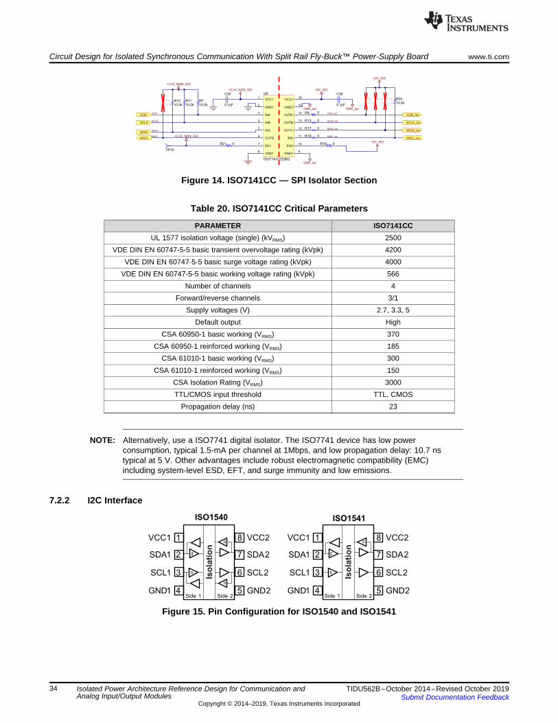
6.2.1 Serial Peripheral Interface (SPI)ISO7141CC (or ISO7741) , a low-power 3/1 quad-channel digital isolator with noise filter, is used to isolateSPI signals. This design is tested up to 4Mbps.
6.2.2 I2C InterfaceISO1541, a low-power, bidirectional I2C isolator, is used to isolate I2C signals.
The I2C is open-drain topology, requiring two lines, serial data (SDA), and serial clock (SCL), to beconnected to VDD by pullup resistors. To have logic Zero online, pull the line to ground (an operatingMOSFET). To have logic One, let the line float (a not-operating MOSFET) to make it High due to thepullup resistor.
Pullup resistors are selected based on recommended drain currents. This design uses 1.5-kΩ pullupresistors and is tested at 100 Kbps.
6.3 LED IndicatorsLED indications for 15-V, –15-V, and 5-V isolated power supplies are provided in this design.
6.4 Input and Output ConnectorsInput connector:• 8-pin screw type terminal blocks for interfacing non-isolated SPI, I2C, and input power
Output connectors:• 8-pin screw type terminal block for interfacing isolated SPI and I2C• 4-pin screw type terminal block for isolated voltage outputs

Buck+
-Vin
Vout
Vin
Vpri
Vsec
1
N
Fly-Buck
Circuit Design for Isolated Synchronous Communication With Split Rail Fly-Buck™ Power-Supply Board www.ti.com
22 TIDU562B–October 2014–Revised October 2019Submit Documentation Feedback
Copyright © 2014–2019, Texas Instruments Incorporated
Isolated Power Architecture Reference Design for Communication andAnalog Input/Output Modules
7 Circuit Design for Isolated Synchronous Communication With Split Rail Fly-Buck™Power-Supply Board
7.1 Power Supply
7.1.1 DC/DC Converter for Generation of Output VoltagesThe Fly-Buck converter is evolved from a synchronous buck converter by adding coupled windings to theinductor to have flyback-like isolated outputs. The isolated outputs can be multiple by adding moresecondary windings to the transformer.
Figure 4. Fly-Buck™ Topology Basics
The Fly-Buck is capable of generating multiple isolated and negative outputs. Fly-Buck topology has betterregulation, better efficiency, and lower cost compared to flyback topology.

FB
VINVCC
SW
RTN
BST
1.225V
VILIM
LM5017
RON
ILIMCOMPARATOR
+
-
V UVLO
ON/OFF
TIMERS
COT CONTROL
LOGIC
1.225V
START-UP
REGULATOR
VIN
FEEDBACK
DISABLE
THERMAL
SHUTDOWN
UVLO
OVER-VOLTAGE1.62V
UVLO
4.5V
SD
SHUTDOWN
VDD REG
BG REF
0.66V
20 µA
CURRENT
LIMIT
ONE-SHOT
www.ti.com Circuit Design for Isolated Synchronous Communication With Split Rail Fly-Buck™ Power-Supply Board
23TIDU562B–October 2014–Revised October 2019Submit Documentation Feedback
Copyright © 2014–2019, Texas Instruments Incorporated
Isolated Power Architecture Reference Design for Communication andAnalog Input/Output Modules
Figure 5. LM5017 Functional Block Diagram
The LM5017 is configured in Fly-Buck topology to generate non-isolated 3.3 V and isolated 5, 15, and –15V from 24-V DC. An isolated Fly-Buck converter uses a coupled inductor windings to generate isolatedoutputs. Flyback topology does not need for an optocoupler or auxiliary winding as the secondary outputclosely tracks the primary output voltage, resulting in a cost effective and smaller-sized solution.
Table 7. Power-Supply Specifications
INPUT — DC NOMINALOUTPUTS ISOLATED — DC OUTPUT NON-ISOLATED — DC
VOLTAGE LOAD VOLTAGE LOAD
24 V15 V 50 mA
3.3 V 25 mA–15 V 50 mA5 V 100 mA

TP8
TP72.2µFC11
TP3
TP1
TP2
+18V_ISO
+6V_ISO
-18V_ISO9.3V_NON_ISO
RTN1
VIN2
UVLO3
RON4
FB5
VCC6
BST7
SW8
EP9
U2
LM5017MRE/NOPB
A2
K1
D12
SDM10U45-7-F
A2
K1
D9DFLS1200-7
A2
K1
D2 DFLS1200-7
A2
K1 D7
PMEG6010CEH,1150.01µFC14 2.2µFC21
2.2µFC22
2.2µFC1
1µFC13
0.47µFC3
10µFC19
+24VDC_LIMIT
GND_iso
GND_iso
27.0kR4
187k
R31
56.2kR32
0.1µF
C42
3300pFC43
60.4kR28
4.87kR29
1 2
L2
3.3µH
2.2µFC2
6
9
8
7
4
31
10
2
5
T1
750342178
1
2
3
4
J1
282834-4
+15V_ISO
-15V_ISO
GND_iso
0.1µFC34
0.1µFC25
+6V_ISO
1000pF
C4
22
11
D8CDSOD323-T24C
GND_iso
A2
K1
D6
DFLS1200-7
0R34
0R35
0R36
340kR30
0
R6
10µFC9
1µFC24
1µFC33
Circuit Design for Isolated Synchronous Communication With Split Rail Fly-Buck™ Power-Supply Board www.ti.com
24 TIDU562B–October 2014–Revised October 2019Submit Documentation Feedback
Copyright © 2014–2019, Texas Instruments Incorporated
Isolated Power Architecture Reference Design for Communication andAnalog Input/Output Modules
Figure 6. Fly-Buck™ Power-Supply Schematic
Table 8. LM5017 Fly-Buck™ Calculation
SPECIFICATIONSNOTE
NAME (V) (A)Vin_min 17Vin_max 32
Vopri 7.9 0Vosec1 5 0.1Vosec2 5 0.1Vosec3 15 0.05Vosec4 15 0.05
η 0.85 Assumed efficiencyfsw 270 kHzRon 344.23 kΩ
Dmax 0.55Dmin 0.29
Toff_min 1.68 µs Toff_min > 0.144 µsVdiode 0.3 V Rectifier diode voltage drop
Nsec1/Npri 0.67Nsec2/Npri 0.67Nsec3/Npri 1.94Nsec4/Npri 1.94
www.ti.com Circuit Design for Isolated Synchronous Communication With Split Rail Fly-Buck™ Power-Supply Board
25TIDU562B–October 2014–Revised October 2019Submit Documentation Feedback
Copyright © 2014–2019, Texas Instruments Incorporated
Isolated Power Architecture Reference Design for Communication andAnalog Input/Output Modules
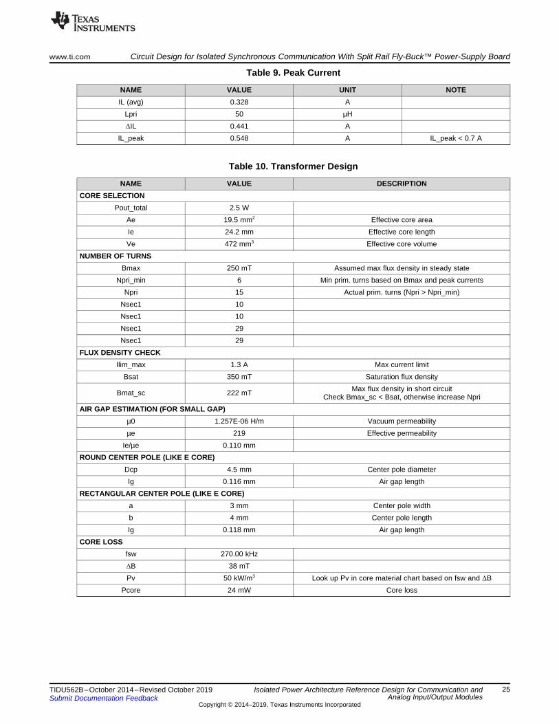
Table 9. Peak Current
NAME VALUE UNIT NOTEIL (avg) 0.328 A
Lpri 50 µHΔIL 0.441 A
IL_peak 0.548 A IL_peak < 0.7 A
Table 10. Transformer Design
NAME VALUE DESCRIPTIONCORE SELECTION
Pout_total 2.5 WAe 19.5 mm2 Effective core areaIe 24.2 mm Effective core lengthVe 472 mm3 Effective core volume
NUMBER OF TURNSBmax 250 mT Assumed max flux density in steady state
Npri_min 6 Min prim. turns based on Bmax and peak currentsNpri 15 Actual prim. turns (Npri > Npri_min)
Nsec1 10Nsec1 10Nsec1 29Nsec1 29
FLUX DENSITY CHECKIlim_max 1.3 A Max current limit
Bsat 350 mT Saturation flux density
Bmat_sc 222 mT Max flux density in short circuitCheck Bmax_sc < Bsat, otherwise increase Npri
AIR GAP ESTIMATION (FOR SMALL GAP)µ0 1.257E-06 H/m Vacuum permeabilityµe 219 Effective permeability
Ie/µe 0.110 mmROUND CENTER POLE (LIKE E CORE)
Dcp 4.5 mm Center pole diameterIg 0.116 mm Air gap length
RECTANGULAR CENTER POLE (LIKE E CORE)a 3 mm Center pole widthb 4 mm Center pole lengthIg 0.118 mm Air gap length
CORE LOSSfsw 270.00 kHzΔB 38 mTPv 50 kW/m3 Look up Pv in core material chart based on fsw and ΔB
Pcore 24 mW Core loss

IN HYSV (HYS) I R28= ´
IN
R28V (UVLO,risin g) 1.225 1
R29
æ ö= ´ +ç ÷
è ø
Circuit Design for Isolated Synchronous Communication With Split Rail Fly-Buck™ Power-Supply Board www.ti.com
26 TIDU562B–October 2014–Revised October 2019Submit Documentation Feedback
Copyright © 2014–2019, Texas Instruments Incorporated
Isolated Power Architecture Reference Design for Communication andAnalog Input/Output Modules
7.1.2 UV ProtectionThe undervoltage lockout (UVLO) circuit allows the input undervoltage threshold and hysteresis to beindependently programmed.
where• R28 = 60.4 kΩ• R29 = 4.87 kΩ (1)
Then, VIN (UVLO, rising) = 16.46 V.
where• IHYS = 0.02 mA (2)
Then, VIN (HYS) = 1.208 V.

TP5
1µFC44
L3
1000 OHM
0.1µFC15
+15V_ISO
OUT1
NC2
SENSE3
6P4V24
6P4V15
3P2V6
GND7
1P6V8
0P8V9
0P4V10
0P2V11
0P1V12
EN13
NR14
IN15
IN16
NC17
NC18
NC19
OUT20
PAD21
U3
TPS7A4700RGW
4.7µFC18
0.1µFC17
18V
A2
K1
D5DZ2W18000L
A2
C1
GreenD3
4.7kR5
GND_isoGND_iso GND_iso GND_iso
GND_iso GND_iso GND_iso
+18V_ISO
10µFC23
47µFC16
www.ti.com Circuit Design for Isolated Synchronous Communication With Split Rail Fly-Buck™ Power-Supply Board
27TIDU562B–October 2014–Revised October 2019Submit Documentation Feedback
Copyright © 2014–2019, Texas Instruments Incorporated
Isolated Power Architecture Reference Design for Communication andAnalog Input/Output Modules
7.1.3 Isolated Output Voltage Regulators
7.1.3.1 Isolated 15 VThe TPS7A4700 is designed with bipolar technology primarily for high-accuracy, high-precisioninstrumentation applications where clean voltage rails are critical to maximize system performance. Thisfeature is a must for powering operational amplifiers, ADCs, DACs, and other high-performance analogcircuitry in critical applications such as medical, radio frequency (RF), and test-and-measurement.
In addition, the TPS7A4700 is ideal for post DC/DC converter regulation. By filtering out the output voltageripple inherent to DC/DC switching conversions, maximum system performance is ensured in sensitiveinstrumentation, test-and-measurement, audio, and RF applications.
Output voltages are user-programmable (up to 20.5 V) using a printed circuit board (PCB) layout withoutthe need of external resistors or feed-forward capacitors, thus reducing overall component count.
Figure 7. TPS7A4700 15-V Regulator
Table 11. TPS7A4700 Critical Parameters
PARAMETER TPS7A4700Output options Programmable outputVIN (Min) (V) 3VIN (Max) (V) 36VOUT (Min) (V) 1.4VOUT (Max) (V) 20.5Iq (Typ) (mA) 0.58
Vdo (Typ) (mV) 216Accuracy (%) 2.5Noise (µVRMS) 4
PSRR at 100 kHz (dB) 68

0.1µFC7
9.42kR1
0.01µFC6
L1
1000 OHM
0.01µF
C41
TP4-15V_ISO
OUT1
FB2
NC
3
GN
D4
EN5
NR
/SS
6
DNC7
VIN8
TP
AD
9 U1TPS7A3001DGNR
4.7µFC10
0.1µFC12
18V
A2
K1
D4DZ2W18000L
A2
C1
GreenD1
4.7kR3
GND_iso
GND_iso GND_iso GND_iso GND_iso
GND_iso GND_iso GND_iso
-18V_ISO
4.7µF
C510µFC8
110kR2
Circuit Design for Isolated Synchronous Communication With Split Rail Fly-Buck™ Power-Supply Board www.ti.com
28 TIDU562B–October 2014–Revised October 2019Submit Documentation Feedback
Copyright © 2014–2019, Texas Instruments Incorporated
Isolated Power Architecture Reference Design for Communication andAnalog Input/Output Modules
7.1.3.2 Isolated –15 VThe TPS7A3001 is a negative, high-voltage (–36 V), ultra low-noise (15.1 µVRMS, 72 dB PSRR) linearregulator. TPS7A3001 includes a CMOS logic-level-compatible enable pin and capacitor-programmablesoft-start function that allows for customized power-management schemes. Other features availableinclude built-in current limit and thermal shutdown protection to safeguard the device and system duringfault conditions.
The TPS7A3001 is designed using bipolar technology and is ideal for high-accuracy, high-precisioninstrumentation applications where clean voltage rails are critical to maximize system performance. Thisdesign is an excellent choice to power operational amplifiers, ADCs, DACs, and other high-performanceanalog circuitry.
In addition, the TPS7A3001 linear regulator is suitable for post DC/DC converter regulation. By filtering outthe output voltage ripple inherent to DC/DC switching conversion, maximum system performance isprovided in sensitive instrumentation, test and measurement, audio, and RF applications.
Figure 8. TPS7A3001 –15-V Regulator
Table 12. TPS7A3001 Critical Parameters
PARAMETER TPS7A3001
Output options Adjustable outputNegative output
VIN (Min) (V) –36VIN (Max) (V) –3VOUT (Min) (V) –33VOUT (Max) (V) –1.2Iq (Typ) (mA) 0.05
Vdo (Typ) (mV) 216Accuracy (%) 2.5Noise (µVRMS) 15
PSRR at 100 kHz (dB) 55

1000pF
C460.1µFC45
0.1µFC32 4.7µF
C27
L4
1000 OHM
TP9
+5V_ISO
OUT1
FB/DNC2
PG3
GND4
EN5
NC6
DELAY7
IN8
9
U5TPS7A1650DGNR
A2
C1
GreenD11
GND_isoGND_isoGND_iso
GND_iso
GND_iso
GND_iso
GND_iso
+6V_ISO
22µFC29
22µFC28 5.9V
D10PTZTE255.6B
GND_iso
1.20kR1220K
R38
11.3KR39
www.ti.com Circuit Design for Isolated Synchronous Communication With Split Rail Fly-Buck™ Power-Supply Board
29TIDU562B–October 2014–Revised October 2019Submit Documentation Feedback
Copyright © 2014–2019, Texas Instruments Incorporated
Isolated Power Architecture Reference Design for Communication andAnalog Input/Output Modules
7.1.3.3 Isolated 5 VAn isolated 5 V is generated using TPS7A1650 linear regulator.
The TPS7A1650 is ultra-low power, low-dropout (LDO) voltage regulator, which offers the benefits of ultra-low quiescent current, high input voltage and miniaturized, high thermal-performance packaging.
The TPS7A1650 is designed for continuous or sporadic (power backup) battery-powered applicationswhere ultra-low quiescent current is critical to extending system battery life.
The TPS7A1650 offers an enable pin (EN) compatible with standard CMOS logic and an integrated opendrain active-high power good output (PG) with a user-programmable delay. These pins are intended foruse in microcontroller-based, battery-powered applications where power rail sequencing is required.
Figure 9. TPS7A1650 5-V Regulator
Table 13. TPS7A1650 Critical Parameters
PARAMETER TPS7A1650Output options Fixed outputVIN (Min) (V) 3VIN (Max) (V) 60
Fixed Output Options (V) 5VOUT (Min) (V) 5VOUT (Max) (V) 5IQ (Typ) (mA) 0.005
Vdo (Typ) (mV) 60Accuracy (%) 2
PSRR at 100 kHz (dB) 26
The isolated SPI and I2C are interfaced with external devices. These external devices can operate on 3.3V or 5 V. Currently, the levels are configured for external devices operating at 5 V . When the slavedevices are operating at 3.3 V, change the following to configure the interface signals to 3.3 V:1. Change U5: Use TPS7A1501 instead of TPS1650.2. Populate R38 and R39 with values shown in the schematic and BOM. Currently, R38 and R39 are
shown as do not populate.
The Fly-Buck design can generate –5 V. There is no requirement for –5 V in the designs this module istargeted to interface with; therefore, the design does not have the –5-V output regulator.

TP69.3V_NON_ISO
0.1µFC30
TP12+3.3V_NON_ISO
10µFC31
IN1
GN
D2
EN3
NC
4O
UT
5
U4TPS70933DBVT
1µFC20
0.1µFC26
0R37
Circuit Design for Isolated Synchronous Communication With Split Rail Fly-Buck™ Power-Supply Board www.ti.com
30 TIDU562B–October 2014–Revised October 2019Submit Documentation Feedback
Copyright © 2014–2019, Texas Instruments Incorporated
Isolated Power Architecture Reference Design for Communication andAnalog Input/Output Modules
7.1.4 3.3-V Non-isolated Output VoltageVCC_NON_ISO is applied to TPS70933 linear regulator that generates 3.3 V_NON_ISO. The 3.3V_NON_ISO is used to power-up SPI and I2C digital isolators.
The TPS70933 linear regulator is an ultra-low, quiescent current device designed for power-sensitiveapplications. A precision band-gap and error amplifier provides 2% accuracy over temperature. Quiescentcurrent of only 1 µA makes TPS70933 ideal solutions for battery-powered, always-on systems that requirevery little idle-state power dissipation. TPS70933 have thermal-shutdown, current-limit, and reverse-current protections for added safety.
This regulator can be put into shutdown mode by pulling the EN pin low. The shutdown current in thismode goes down to 150 nA, typically.
Figure 10. TPS70933 3.3-V Regulator
Table 14. TPS70933 Critical Parameters
PARAMETER TPS70933Output options Fixed outputVIN (Min) (V) 2.7VIN (Max) (V) 30
Fixed Output Options (V) 3.3VOUT (Min) (V) 3.3VOUT (Max) (V) 3.3Iq (Typ) (mA) 0.001
Vdo (Typ) (mV) 300Accuracy (%) 2
PSRR at 100kHz (dB) 26

www.ti.com Circuit Design for Isolated Synchronous Communication With Split Rail Fly-Buck™ Power-Supply Board
31TIDU562B–October 2014–Revised October 2019Submit Documentation Feedback
Copyright © 2014–2019, Texas Instruments Incorporated
Isolated Power Architecture Reference Design for Communication andAnalog Input/Output Modules
7.1.5 Power-Supply Performance
Table 15. Current Consumption for SPI and I2C Isolators
DEVICE NON-ISOLATED SIDE — CURRENT AT3.3 V
ISOLATED SIDE — CURRENTAT 5 V
SPI 3.5 mA 9.6 mAI2C 3.5 mA 3.5 mA
Table 16. Maximum Power on Output Voltages
OUTPUT VOLTAGE POWER15 V 0.8 W–15 V 0.8 W
5 V 0.55 W3.3 V 0.1 W
Table 17. Efficiency Calculation
NAME VALUEOutput power 2.25 WInput power 3.1 WEfficiency >72%

Vin
Err
or
(%
)
16 18 20 22 24 26 28 30 32 34
-4%
-3%
-2%
-1%
0
1%
2%
3%
+15V
+5V
-15V
Load Current (%)
Eff
icie
nc
y
0 10% 20% 30% 40% 50% 60% 70% 80% 90% 100%
0
10%
20%
30%
40%
50%
60%
70%
80%
17Vin
24Vin
32Vin
Circuit Design for Isolated Synchronous Communication With Split Rail Fly-Buck™ Power-Supply Board www.ti.com
32 TIDU562B–October 2014–Revised October 2019Submit Documentation Feedback
Copyright © 2014–2019, Texas Instruments Incorporated
Isolated Power Architecture Reference Design for Communication andAnalog Input/Output Modules
Figure 11. Efficiency Plot
Figure 12. Line Regulation at 100% Load
7.1.6 Recommendations for Power Supply
1. Power supply must be on before SPI or I2C communication is initiated.2. Do not hot swap the input and output power.3. Do not apply overvoltage >30 V at the input.

1
2
3
4
5
6
7
8
ISO7140
9
10
11
12
13
14
15
16
NC
INA
GND1
GND2
GND2
INB
INC
OUTA
OUTC
OUTB
EN
IND OUTD
1
2
3
4
5
6
7
8 9
10
11
12
13
14
15
16
INA
GND2
GND2
INB
OUTC
OUTA
INC
OUTB
NC
EN2EN1
VCC1
GND1GND1
VCC2
GND1
VCC1
NC
VCC2
ISO7131
1
2
3
4
5
6
7
8 9
10
11
12
13
14
15
16
INA
GND2
GND2
INB
INC
OUTA
OUTC
OUTB
IND
EN2EN1
GND1
GND1
VCC1
OUTD
VCC2
ISO7141
www.ti.com Circuit Design for Isolated Synchronous Communication With Split Rail Fly-Buck™ Power-Supply Board
33TIDU562B–October 2014–Revised October 2019Submit Documentation Feedback
Copyright © 2014–2019, Texas Instruments Incorporated
Isolated Power Architecture Reference Design for Communication andAnalog Input/Output Modules
7.2 Signal Isolation
7.2.1 Serial Peripheral Interface (SPI)
Figure 13. Pin Configuration for ISO7141CC (Top View)
(1) VCCx is the supply voltage, VCC1 or VCC2, for the output channel that is being measured.
Table 18. Output — High and Low Levels for ISO7141CC
PARAMETER TEST CONDITIONS MIN TYP MAX UNIT
VOH High-level output voltageIOH = –4 mA VCCx
(1) – 0.5 4.8V
IOH = –20 µA VCCx(1) – 0.1 5
VOL Low-level output voltageIOL = 4 mA 0.2 0.4
VIOL = 20 µA 0 0.1
Table 19. Input Levels for ISO7141CC
PARAMETER MIN TYP MAX UNIT
IOHHigh-level output current (VCC ≥ 3.0 V) –4 mAHigh-level output current (VCC < 3.0 V) –2 mA
IOL Low-level output current 4 mAVIH High-level input voltage 2 VCC VVIL Low-level input voltage 0 0.8 V
This design is tested for the application requirement speed up to 4 Mbps.
ISO7141CC provide galvanic isolation up to 2500 VRMS for one minute per UL and 4242 VPK per VDE.ISO7141 is quad-channel isolator with three forward and one reverse-direction channels. ISO7141CC iscapable of a 50-Mbps maximum data rate with a 5-V supply and a 40-Mbps maximum data rate with a3.3-V or 2.7-V supply, with integrated filters on the inputs for noise-prone applications. The default outputstate is high as required for SPI.
Each isolation channel has a logic input and output buffer separated by a silicon dioxide (SiO2) insulationbarrier. Used in conjunction with isolated power supplies, this device prevents noise currents on a databus or other circuits from entering the local ground and interfering with or damaging sensitive circuitry. Thedevice has TTL input thresholds and can operate from 2.7-V, 3.3-V, and 5-V supplies. All inputs are 5-Vtolerant when supplied from a 2.7-V or 3.3-V supply.
ISO1540 ISO1541
1
2
3
4 5
6
7
8
GND2
SCL1
VCC2VCC1
SCL2
GND1
SDA1 SDA2
Side 1 Side 2
Iso
lati
on
1
2
3
4 5
6
7
8
GND2
SCL1
VCC2VCC1
SCL2
GND1
SDA1 SDA2
Side 1 Side 2
Iso
lati
on
VCC11
GND12
INA3
INB4
INC5
OUTD6
EN17
GND18
GND29
EN210
IND11
OUTC12
OUTB13
OUTA14
GND215
VCC216
U6
ISO7141CCDBQ
MISO MISO_isoMISO_iso
+3.3V_NON_ISO +5V_ISO
0.1µF
C35
0.1µF
C36
+5V_ISO
+3.3V_NON_ISO
GND_iso
GND_iso
GND_iso
MOSIMOSI_iso
MOSI_iso
MISO
MOSI
/CS0_iso/CS0_iso
SCLK_isoSCLK_iso
SCLK
/CS0/CS0
SCLK
TP10
+3.3V_NON_ISO
+5V_ISO
0R8
10.0kR7
0R13
0R17
0R18
10.0kR9
10.0kR10
10.0kR11
10.0kR14
10.0kR15
10.0kR19
10.0kR20
0R160R21
Circuit Design for Isolated Synchronous Communication With Split Rail Fly-Buck™ Power-Supply Board www.ti.com
34 TIDU562B–October 2014–Revised October 2019Submit Documentation Feedback
Copyright © 2014–2019, Texas Instruments Incorporated
Isolated Power Architecture Reference Design for Communication andAnalog Input/Output Modules
Figure 14. ISO7141CC — SPI Isolator Section
Table 20. ISO7141CC Critical Parameters
PARAMETER ISO7141CCUL 1577 isolation voltage (single) (kVRMS) 2500
VDE DIN EN 60747-5-5 basic transient overvoltage rating (kVpk) 4200VDE DIN EN 60747-5-5 basic surge voltage rating (kVpk) 4000
VDE DIN EN 60747-5-5 basic working voltage rating (kVpk) 566Number of channels 4
Forward/reverse channels 3/1Supply voltages (V) 2.7, 3.3, 5
Default output HighCSA 60950-1 basic working (VRMS) 370
CSA 60950-1 reinforced working (VRMS) 185CSA 61010-1 basic working (VRMS) 300
CSA 61010-1 reinforced working (VRMS) 150CSA Isolation Rating (VRMS) 3000TTL/CMOS input threshold TTL, CMOS
Propagation delay (ns) 23
NOTE: Alternatively, use a ISO7741 digital isolator. The ISO7741 device has low powerconsumption, typical 1.5-mA per channel at 1Mbps, and low propagation delay: 10.7 nstypical at 5 V. Other advantages include robust electromagnetic compatibility (EMC)including system-level ESD, EFT, and surge immunity and low emissions.
7.2.2 I2C Interface
Figure 15. Pin Configuration for ISO1540 and ISO1541

VCC11
SDA12
SCL13
GND14
GND25
SCL26
SDA27
VCC28
U7
ISO1541D
+5V_ISO
0.1µF
C40
GND_iso
GND_iso
+3.3V_NON_ISO
0.1µF
C39
TP11
TP13
SCLSCL_isoSCL
SDA SDA_iso
+3.3V_NON_ISO+5V_ISO
1.50k
R261.50kR24
1.50kR22
1.50kR23
0R27
0R25
SDA
SCL_iso
SDA_iso
www.ti.com Circuit Design for Isolated Synchronous Communication With Split Rail Fly-Buck™ Power-Supply Board
35TIDU562B–October 2014–Revised October 2019Submit Documentation Feedback
Copyright © 2014–2019, Texas Instruments Incorporated
Isolated Power Architecture Reference Design for Communication andAnalog Input/Output Modules
Table 21. Input and Output Levels for ISO1541
PARAMETER MIN NOM MAX UNITVCC1, VCC2 Supply voltage 3 5.5
V
VSDA1, VSCL1 I/O signal voltages, side 1 0 VCC1VSDA2, VSCL2 I/O signal voltages, side 2 0 VCC2
VIL1 Low-level input voltage, side 1 0 0.5VIH1 High-level input voltage, side 1 0.7 × VCC1 VCC1VIL2 Low-level input voltage, side 2 0 0.3 × VCC2VIH2 High-level input voltage, side 2 0.7 × VCC2 VCC2
The ISO1541 is a low-power, bidirectional isolator that is compatible with I2C interfaces. This device haslogic input and output buffers separated by TI’s capacitive isolation technology using a SiO2 barrier. Whenused in conjunction with isolated power supplies, this device blocks high voltages, isolates grounds, andprevents noise currents from entering the local ground and interfering with or damaging sensitive circuitry.
This isolation technology provides for function, performance, size, and power consumption advantageswhen compared to optocouplers. The ISO1541 enable a complete isolated I2C interface to beimplemented within a small form factor.
The ISO1541 has a bidirectional data and a unidirectional clock channel. The ISO1541 is useful inapplications that have a single master while the ISO1540 is ideally fit for multi-master applications.
Isolated bidirectional communications is accomplished within ISO1541 by offsetting the side one low-leveloutput voltage to a value greater than the side one high-level input voltage thus preventing an internallogic latch that otherwise would occur with standard digital isolators.
Figure 16. ISO1541 — I2C Isolator
Table 22. ISO1541 Critical Parameters
PARAMETER ISO1541UL 1577 isolation voltage (single) (kVRMS) 2.5
VDE DIN EN 60747-5-5 basic transient overvoltage rating (kVpk) 4.3VDE DIN EN 60747-5-5 basic surge voltage rating (kVpk) 4
VDE DIN EN 60747-5-5 basic working voltage rating (kVpk) 0.0566CSA isolation rating (VRMS) 2.8
CSA 60950-1 basic working (VRMS) 390CSA 61010-1 basic working (VRMS) 300
CSA 61010-1 reinforced working (VRMS) 150Data rate (Mbps) 1
Number of channels 2Serial clock UnidirectionalSerial data Bidirectional

VCC1 VCC2
GND1 GND2
8
7
4 54
XOUT
XIN
5
6
2
MSP430
G2132
1
2
3 ISO1541
DVss
DVcc
0.1 Fμ0.1 Fμ 0.1 Fμ
6SDA
SCL
9
8
10 Fμ
VS
0.1 Fμ
MBR0520L
MBR0520L
1:2.2
0.1 Fμ
3
1
D2
SN6501
D1
Vcc
4,5
2
GND
3.3V
IN
ON GND
OUT1 5
23LP2981-50 10 Fμ
10 Fμ
SDA2SDA1
SCL1 SCL2
1.5k 1.5k 1.5k 1.5k
0.1 Fμ
8
VDD
GND
AIN0
2
1
9
10SDA
SCL
4
ADDR
ADS1115
AIN3RDY
3
4 Analog
Inputs
7
VIN
GND
VOUT26
4REF5040
1 Fμ22μF0.1 Fμ
4
VDD
VOUTA11
10SDA
SCL
1
DAC8574
VOUTD8GND
6
12 3
VREFHA2
15
IOVDD
VREFL
5
4 Analog
Outputs
A3
16
A0
13
9
14LDAC
A1
5VISO
5VISO
5VISO
5VISO
SD
A
SC
LISO-BARRIER
1Ω
Circuit Design for Isolated Synchronous Communication With Split Rail Fly-Buck™ Power-Supply Board www.ti.com
36 TIDU562B–October 2014–Revised October 2019Submit Documentation Feedback
Copyright © 2014–2019, Texas Instruments Incorporated
Isolated Power Architecture Reference Design for Communication andAnalog Input/Output Modules
(1) H = High level; L = Low level; Z = High impedance or float; X = Irrelevant; ? = Indeterminate.(2) Invalid input condition as an I2C system requires that a pullup resistor to VCC is connected.
Table 23. Pullup Recommendations for I2C Interface (1)
POWER STATE INPUT OUTPUTVCC1 or VCC2 < 2.1 V X Z
VCC1 and VCC2 > 2.8 V L LVCC1 and VCC2 > 2.8 V H ZVCC1 and VCC2 > 2.8 V Z (2) ?
For I2C interface, a pullup on the input side and the output side of the isolator is recommended.
Figure 17. Illustration for I2C Interface With Pullups
In Figure 17, the ultra low-power microcontroller MSP430G2132 controls the I2C data traffic ofconfiguration data and conversion results for the analog inputs and outputs (see datasheet). Low-powerdata converters build the analog interface to sensors and actuators. The ISO1541 provides the necessaryisolation between different ground potentials of the system controller, remote sensor, and actuator circuitryto prevent ground loop currents that otherwise may falsify the acquired data.
The entire circuit operates from a single 3.3-V supply. A low-power push-pull converter, SN6501, drives acenter-tapped transformer whose output is rectified and linearly regulated to provide a stable 5-V supplyfor the data converters.
7.3 LED IndicatorsThe LEDs are provided for indicating the status of the output voltages. SMD LEDs are used for indicationpurpose. These LEDs are continuously ON when output voltages are present.

1
2
3
4
J1
282834-4
+15V_ISO
-15V_ISO
GND_iso
0.1µFC34
0.1µFC25
+6V_ISO
GND_iso
0R34
0R35
0R361µFC24
1µFC33
5
4
1
2
3
6
7
8
1725711
J3
/CS0_iso
SCLK_iso
MOSI_iso
MISO_iso
SDA_iso
SCL_iso
GND_iso
0R33
+5V_ISO
0.1µFC38
GND_iso
1µFC37
/CS0_iso
SCLK_iso
MOSI_iso
MISO_iso
SCL_iso
SDA_iso
5
4
1
2
3
6
7
8
1725711
J2
MISO
MOSI
SCLK
/CS0
+24VDC_LIMIT
SDA
SCL
/CS0
SCLK
MOSI
MISO
SCL
SDA
www.ti.com Circuit Design for Isolated Synchronous Communication With Split Rail Fly-Buck™ Power-Supply Board
37TIDU562B–October 2014–Revised October 2019Submit Documentation Feedback
Copyright © 2014–2019, Texas Instruments Incorporated
Isolated Power Architecture Reference Design for Communication andAnalog Input/Output Modules
7.4 Input and Output ConnectorsInput Connector8-pin screw type terminal blocks are used for interfacing non-isolated SPI, I2C, and input power.
Figure 18. Non-isolated SPI, I2C, and Power Input Connector
Output ConnectorAn 8-pin screw type terminal block is used for interfacing isolated SPI and I2C.
Figure 19. Isolated SPI and I2C Output Connector
A 4-pin screw type terminal block is used for isolated voltage outputs.
Figure 20. Isolated Output Voltage Connector

Circuit Design for Isolated Synchronous Communication With Split Rail Fly-Buck™ Power-Supply Board www.ti.com
38 TIDU562B–October 2014–Revised October 2019Submit Documentation Feedback
Copyright © 2014–2019, Texas Instruments Incorporated
Isolated Power Architecture Reference Design for Communication andAnalog Input/Output Modules
7.5 PCB Design Guidelines and Dimensions
• Apply creepage and clearance requirements according to the specific application isolation standards.Take care to maintain these distances on a board design to ensure that the mounting pads for theisolator do not reduce this distance. Creepage and clearance on the printed-circuit board becomeequal in certain cases. Use techniques such as inserting grooves and ribs on the PCB to help increasethese specifications.
• Use an SMD ceramic bypass capacitor of approximately 0.1 μF in value.• Use a continuous ground plane to provide a low-impedance signal return path as well as generating
the lowest EMI signature by reducing phenomena such as unintended current loops.• PCB material: Standard FR-4 epoxy-glass as PCB material is preferred for industrial applications with
a speed less than 100 MHz I. FR-4 (Flame Retardant 4) meets the requirements of UnderwritersLaboratories UL94-V0 and is preferred over cheaper alternatives due to its lower dielectric losses athigh frequencies, less moisture absorption, greater strength and stiffness, and its self-extinguishing,flammability characteristics.
• Trace Routing: Use 45° bends (chamfered corners), instead of right-angle (90°) bends. Right-anglebends increase the effective trace width and thus the trace impedance. This creates additionalimpedance mismatch, which may lead to higher reflections.
NOTE: The PCB is designed as a small add-on board. This board has provision for isolated powersupply, SPI, and I2C interface. There may be some applications where 15- and –15-Visolated power supplies are available. In this case, the LM5017 Fly-Buck part may not berequired.

Power SelectSwitch Green Power LED
USB Connector(Power/ICDI)
Reset Switch
RGB User LED
User Switch 2User Switch 1
USB Micro-A/-BConnector(Device)
Tiva C SeriesLaunchPadBoosterPack XLInterface (J1, J2, J3,and J4 Connectors)
Tiva C SeriesLaunchPadBoosterPack XLInterface (J1, J2, J3,and J4 Connectors)
MSP430LaunchPad-CompatibleBoosterPack Interface
MSP430LaunchPad-CompatibleBoosterPack Interface
TivaTM4C123GH6PMIMicrocontroller
TivaTM4C123GH6PMIMicrocontroller
www.ti.com Circuit Design for Isolated Synchronous Communication With Split Rail Fly-Buck™ Power-Supply Board
39TIDU562B–October 2014–Revised October 2019Submit Documentation Feedback
Copyright © 2014–2019, Texas Instruments Incorporated
Isolated Power Architecture Reference Design for Communication andAnalog Input/Output Modules
7.6 Tiva™ C Series LaunchPad™ InterfaceThe Tiva C Series LaunchPad (EK-TM4C123GXL) is a low-cost evaluation platform for Arm® Cortex®-M4F-based microcontrollers. The Tiva C Series LaunchPad design highlights the TM4C123GH6PMImicrocontroller USB 2.0 device interface, hibernation module, and motion control pulse-width modulator(MC PWM) module. The Tiva C Series LaunchPad also features programmable user buttons and an RGBLED for custom applications. The stackable headers of the Tiva C Series LaunchPad BoosterPack XLinterface demonstrate how easy it is to expand the functionality of the Tiva C Series LaunchPad wheninterfacing to other peripherals on many existing BoosterPack add-on boards as well as future products.Figure 21 shows a photo of the Tiva C Series LaunchPad.
Figure 21. Tiva™ C Series TM4C123G LaunchPad™ Evaluation Board

Tiva TMC123GXL
LaunchPadTM
(Master)
Isolated Comm Board
Tiva TM4C123GXL
LaunchPadTM
(Slave)
PCPC
SCL
SDA
GND
SCL
SDA
Iso_GND
USB Debug USB Debug
Software Description www.ti.com
40 TIDU562B–October 2014–Revised October 2019Submit Documentation Feedback
Copyright © 2014–2019, Texas Instruments Incorporated
Isolated Power Architecture Reference Design for Communication andAnalog Input/Output Modules
8 Software DescriptionThe code was developed, compiled, and tested in a CCS environment.
8.1 I2C Communication Interface Between Master and Slave
Figure 22. I2C Communication Test Setup
I2C uses one bi-directional pin serial data line (SDA) and one unidirectional serial clock line (SCL):• Master node — generates the clock and initiates communication with slaves• Slave node — receives the clock and responds when addressed by the master
8.1.1 I2C Master
Initializing I2C MasterTo initialize the I2C master functionality:1. Enable the I2C peripheral.2. Enable the clock gating to the SDA and SCL pins.3. Choose the pin configuration for SCL and SDA pins.4. If the I2C device is a master, then enable the master functionality, clock source, and speed of
communication.5. Internal pull up resistors are required when external pull up resistors are not available for SCL and
SDA pins.

www.ti.com Software Description
41TIDU562B–October 2014–Revised October 2019Submit Documentation Feedback
Copyright © 2014–2019, Texas Instruments Incorporated
Isolated Power Architecture Reference Design for Communication andAnalog Input/Output Modules
Depending on the processor platform, the pin mapping would change. Figure 23 is an example codesnippet for I2C initialization.
Figure 23. I2C Master Initialization Code
Sending Data on I2CTo send data on I2C:1. Set the slave address with whom the master would like to communicate.2. Set the data.3. Set the master to transmit mode (single-byte or a multiple-byte stream).4. Wait until the master completes sending the data.
Figure 24 shows an example of I2C master data sending.
Figure 24. I2C Master Data Sending Code

Software Description www.ti.com
42 TIDU562B–October 2014–Revised October 2019Submit Documentation Feedback
Copyright © 2014–2019, Texas Instruments Incorporated
Isolated Power Architecture Reference Design for Communication andAnalog Input/Output Modules
Receiving Data on I2CTo receive data on I2C bus:1. Set the slave address which sends the data.2. Set the master to receive mode (could be single byte or a burst stream)3. Receive the data.4. Check for errors.
Figure 25 is a code snippet for receiving data on I2C:
Figure 25. I2C Master Receiving Code
Optionally, interrupts can be used to receive data.

www.ti.com Software Description
43TIDU562B–October 2014–Revised October 2019Submit Documentation Feedback
Copyright © 2014–2019, Texas Instruments Incorporated
Isolated Power Architecture Reference Design for Communication andAnalog Input/Output Modules
8.1.2 I2C Slave
Initializing I2C SlaveTo initialize the I2C slave functionality:1. Enable the I2C peripheral.2. Enable the clock gating to the SDA and SCL pins.3. Choose the pin configuration for SCL and SDA pins.4. Use internal pull up resistors when external pullup resistors are not available for SCL and SDA pins.
(Since the Tiva Microcontroller is used as the I2C slave, use an external pull up on the slave side aswell.)
5. Select Slave Enable.
Depending on the processor platform, the pin mapping changes. Figure 26 is an example code snippet forI2C initialization.
Figure 26. I2C Slave Initialization Code
Sending Data on I2CTo send data on I2C bus: I2CSlaveDataPut(I2C0_BASE, ui32DataTx);
Checking the Slave StatusTo check the slave status: Error_Status = I2CSlaveStatus(I2C0_BASE);
Receiving Data on I2CTo receive data from master on I2C bus: first_byte = I2CSlaveDataGet(I2C0_BASE);

Tiva TMC123GXL
LaunchPadTM
(Master)
Isolated Comm Board
Tiva TM4C123GXL
LaunchPadTM
(Slave)
PCPC
SCLK SCLK
MOSI
MISO
USB Debug USB Debug
GND Iso_GND
MISO
MOSI
/CS0/CS0
Software Description www.ti.com
44 TIDU562B–October 2014–Revised October 2019Submit Documentation Feedback
Copyright © 2014–2019, Texas Instruments Incorporated
Isolated Power Architecture Reference Design for Communication andAnalog Input/Output Modules
8.2 SPI Communication Interface Between Master and SlaveThe Tiva LaunchPad is used as master and slave. The SPI is configured to work up to 4Mbps. The SPIcommunication uses the following pins:• /CS: Chip select used by the master to select the slave to initiate the communication• SCLK: Clock generated by the master• MISO: Pin used by the slave to transmit data and the master to receive• MOSI: Pin used by the master to transmit data and the slave to receive
Figure 27. SPI Communication Test Setup
NOTE: Host can also be referred as Master.
8.2.1 Initializing the SPITo initialize the SPI:1. Choose master or slave through the macro.2. Enable clock gating to the SPI peripheral.3. Enable and configure the GPIO peripheral pins for SPI mode (clock, chip select, RX and TX).4. Set the SPI to master or slave mode and select the speed.5. Enable the SPI module.

www.ti.com Software Description
45TIDU562B–October 2014–Revised October 2019Submit Documentation Feedback
Copyright © 2014–2019, Texas Instruments Incorporated
Isolated Power Architecture Reference Design for Communication andAnalog Input/Output Modules
Figure 28. SPI Initialization Code

Software Description www.ti.com
46 TIDU562B–October 2014–Revised October 2019Submit Documentation Feedback
Copyright © 2014–2019, Texas Instruments Incorporated
Isolated Power Architecture Reference Design for Communication andAnalog Input/Output Modules
8.2.2 Sending Data on SPITo send data on the SPI:1. Ensure the slave chip select is enabled.2. Send the data.3. Wait until the data is transmitted.
Figure 29. SPI Data Sending Code
8.2.3 Receiving Data on SPITo receive data on SPI, use the receive routine. Data can be received by either polling (in a blocking ornon-blocking way) or using interrupts. Figure 30 demonstrates blocking receive function.
Figure 30. SPI Blocking Receive Function Code

www.ti.com Hardware, Testing Requirements, and Test Results
47TIDU562B–October 2014–Revised October 2019Submit Documentation Feedback
Copyright © 2014–2019, Texas Instruments Incorporated
Isolated Power Architecture Reference Design for Communication andAnalog Input/Output Modules
9 Hardware, Testing Requirements, and Test ResultsThis section provides details of the setup and testing done on the TIDA-00300 reference design tovalidating the performance:• Required hardware connection• Test setup• Functional testing and performance testing• Waveforms
9.1 Required Hardware ConnectionThe following boards and equipment are required for validating the functionality and performance:• TIDA-00300 power supply board for IO and communication modules with basic functional tests
completed• Programmable DC voltage source capable of varying the voltage between 5 V to 30 V with a
programmable current limit up to 1 A• Electronic load for testing the power-supply outputs• Digital multimeter with sufficient resolution for measuring the DC output voltages
9.2 Test Setup for Synchronous Communication BoardUse the following setup to test the isolated and non-isolated power supply performance (see Figure 31).DC power supply, electronic loads, multimeter, and CROs are used to check the power supplyperformance.
Figure 31. Test Setup for TIDA-00300

Hardware, Testing Requirements, and Test Results www.ti.com
48 TIDU562B–October 2014–Revised October 2019Submit Documentation Feedback
Copyright © 2014–2019, Texas Instruments Incorporated
Isolated Power Architecture Reference Design for Communication andAnalog Input/Output Modules
9.3 Testing and ResultsTesting of the design includes the following:• Functional testing• Performance testing
9.3.1 Functional TestingThis section provides details of the functional tests performed, including observations.
9.3.1.1 Isolated Power Supplies for Communication ModuleThis section provides details of the tests done and the test observations for isolated power supplies usingthe DC/DC power module, transformer driver, and digital isolator with integrated power from a 5-V input
Table 24. Isolated Power Supply for Communication Connection Details andMeasurements
POWER SUPPLY INPUT INPUT CONNECTOR OUTPUT MEASUREMENT (V)5-V DC input J7-1: input C104: 5 V 5.15
J7-2: Ground TP51: 5 V 4.97TP53: 3.3 V 3.26TP52: Gnd
J1-1: input TP2: 6 V 6.3J1-2: Ground TP7: 3.3 V 3.255
TP6: GndJ2-1: input TP1: 6 V 6.1
J2-2: Ground TP8: 5 V 4.93TP5: Gnd
J8-1: input TP55: P_13 13.1J8-2: Ground TP59: N_13 13.1
TP56: P_12 12.15TP60: N_12 12.08TP58: Gnd
J4-2: input TP29: LS output 4.88J4-1: Ground TP12: 5.4 V 5.42
TP28: 5 V 5.02TP19: 3.3 V 3.31
J6-1, J5-2: input TP36: LS_Out 4.78J6-2: Ground TP39: LS_Out1 4.78
TP24: 5.4 V 5.38TP25: 5.4 V 5.38TP30: 3.3 V 3.28TP38: 3.3 V 3.28TP33: 5 V 5.01TP41: 5 V 4.95LED_23 OKLED_24 OK
9.3.1.1.1 Testing Isolated DC/DC Converter Functional ModesThis section provides details of different functional modes configured for isolated DC/DC converterUCC12050 and the observations.

www.ti.com Hardware, Testing Requirements, and Test Results
49TIDU562B–October 2014–Revised October 2019Submit Documentation Feedback
Copyright © 2014–2019, Texas Instruments Incorporated
Isolated Power Architecture Reference Design for Communication andAnalog Input/Output Modules
Table 25. Device Functional Modes and Observations
EN SEL ISOLATED SUPPLY OUTPUTVOLTAGE (VISO) SET POINT
LOAD CURRENT INPUT CURRENT MEASUREDVOLTAGE
HIGH Shorted to VISO 5.0 V 100 173 4.98HIGH Shorted to VISO 5.0 V 150 281 3.71HIGH 100 kΩ to VISO 5.4 V 100 206 5.37HIGH 100 kΩ to VISO 5.4 V 10 55 5.37HIGH 100 kΩ to VISO 5.4 V 5 49 5.37HIGH Shorted to GNDS 3.3 V 100 152 3.28HIGH 100 kΩ to GNDS 3.7 V 100 149 3.67HIGH OPEN UNSUPPORTEDLOW X 0 V 0 0
9.3.1.1.2 Additional Isolated DC/DC Converter TestingThis section provides details of the tests performed on the isolated DC/DC using a current limited source.
Table 26. Testing With Current Controller Source
INPUTVOLTAGE
CURRENT LIMIT(mA)
INPUT CURRENT(mA)
OUTPUTSELECTION
OUTPUTVOLTAGE (V)
OUTPUTCURRENT (mA)
5 50 .049 5 4.97 No load5 50 .044 5.4 5.37 No load5 120 .098 5 4.97 505 150 .101 5.4 5.37 505 230 .169 5 4.98 1005 250 .194 5.4 5.37 1005 230 .181 5 3.18 2005 400 .242 5 0.05 short5 400 .242 5.4 0.05 short
9.3.1.1.3 Testing ProtectionThis section provides details of the tests done for checking protection against input voltage variation.
Table 27. Testing UVLO
ISOLATED SUPPLY OUTPUT VOLTAGE (VISO) SET POINT MEASURED VOLTAGE5.0 V 4.985.4 V 5.37UVLO – rising 4.3UVLO – falling 3.7

Hardware, Testing Requirements, and Test Results www.ti.com
50 TIDU562B–October 2014–Revised October 2019Submit Documentation Feedback
Copyright © 2014–2019, Texas Instruments Incorporated
Isolated Power Architecture Reference Design for Communication andAnalog Input/Output Modules
9.3.1.2 Wide Input Isolated Power Supply for Analog IO ModulesThis section provides details of the tests done and the test observations for the split-rail power suppliesgenerated using DC/DC from 24-V or 5-V input.
Table 28. Isolated Power Supply for IO Connection Details and Measurements
POWER SUPPLYINPUT
INPUT OUTPUT MEASUREMENT (V)
5-V DC input J1-1: Input TP43: 5 V 4.996J1-2: Ground J6-1: Ground
24-V input DC/DC J4-1: input J6-2: 5 V 5.126J4-2: Ground J6-1: Ground
TP1: +14 V 14.8TP2: –14 V 14.91
TP29: +12 V 12.08TP31: –12 V 12.28
R23: LDO+5 V 5.11R40: LDO-5 V 4.996
TP6: REF_2.5V_A 2.501TP5: REF_2.5 V 2.494
TP49: +3.3 V 3.288
9.3.1.3 Isolated Synchronous Communication With Split-Rail Fly-Buck™ PowerThis section provides details of the tests done and the test observations for supply rails generated using24-V input with DC/DC configured in Fly-Buck configuration.
Table 29. Fly-Buck™ Test Results at 24-V and 5-V Input
POWER SUPPLYINPUT
INPUT OUTPUT MEASUREMENT (V)
24-V input J2-1: input J1-1: Iso_P_15V 15.27J2-6: Ground J1-2: Iso_M_15V 14.87
J1-3: Iso_P_5V 4.959TP10: Non_Iso_3.3V 3.22
J1-4: GndJ2-2: /CS0 J3-2: /CS0_Iso OKJ2-3: SCLK J3-3: SCLK_Iso OKJ2-4: MOSI J3-4: MOSI_Iso OKJ2-5: MISO J3-5: MISO_Iso OKJ2-7: SDA J3-4: SDA_Iso OKJ2-8: SCL J3-5: SCL_Iso OK
5-V input DC/DC J4-1: input TP15: Iso1_P_15V 15.7J4-2: Ground TP17: Iso1_N_15V 15.7
TP20: Iso1_P_5V 5.06C58: Gnd_Iso1

www.ti.com Hardware, Testing Requirements, and Test Results
51TIDU562B–October 2014–Revised October 2019Submit Documentation Feedback
Copyright © 2014–2019, Texas Instruments Incorporated
Isolated Power Architecture Reference Design for Communication andAnalog Input/Output Modules
9.3.2 Performance TestingThis section provides details of the performance tests including EMI tests that were performed usingTIDA-00300.
9.3.2.1 EMI Performance of DC/DC Converters With 24-V InputThe radiated emission for the DC/DC converter with the following configuration and 24-V input was tested:• LM5160 configured to generate ±15 V and 5 V using the PMP10532 device• LM5017 configured to generate ±15 V and ±5 V using the PMP7993 device
Figure 32 shows the radiated emission plot.
Figure 32. Wide Input DC/DC With Split-Rail EMI Plot
9.3.2.2 EMI Performance of DC/DC Converters With 5-V input Connected to J1, J2, J7The radiated emission using a DC/DC converter with the following configuration was tested:• DCR010505P configured for 5-V output loaded to 100-mA load• DCP010505BP configured for 5-V output loaded to 100-mA load• LP2985AIM5-3.3 configured for 3.3-V output loaded to 50-mA load• SN6505B configured for 6-V output loaded to 200-mA load• SN6501 configured for 6-V output loaded to 100-mA load• TPS70933 configured for 3.3-V output and loaded to 50 mA• TPS70950 configured for 5-V output and loaded to 50 mA
Figure 33 shows the radiated emission plot.

Hardware, Testing Requirements, and Test Results www.ti.com
52 TIDU562B–October 2014–Revised October 2019Submit Documentation Feedback
Copyright © 2014–2019, Texas Instruments Incorporated
Isolated Power Architecture Reference Design for Communication andAnalog Input/Output Modules
Figure 33. SN6505B + SN6501 + DCR010505 + LDO + RE
9.3.2.3 EFT and Surge Test Setup, TIDA-00300 Boards Test Method, Acceptance Criteria and ResultsEFT and surge testing was done on the TIDA-00300 boards with the following test conditions:• 240-V AC supply connected to the TIDA-00227 and TIDA-00227 reference design power-supply output
connected to the TIDA-00300 boards
Table 30 summarizes surge and EFT test results for TIDA-00300 boards connected to the output of theTIDA-00227 power supply with 240-V AC input.
Table 30. Test Results for TIDA-00300 Boards Connected to TIDA-00227
TEST TYPE ANDSTANDARD VOLTAGE LEVEL MEASUREMENT BEFORE TEST MEASUREMENT AFTER TEST
EFT IEC61000-4-4 ±1 kV, 5 kHz, 100 kHz 12 V: 12.06 V, Iso_P_15V: 15.27 V 12 V: 12.06 V, Iso_P_15V: 15.27 VEFT IEC61000-4-4 ±2 kV, 5 kHz, 100 kHz for 1 minute 12 V: 12.06 V, Iso_P_15V: 15.27 V 12 V: 12.06 V, Iso_P_15V: 15.27 V
EFT IEC61000-4-4 ±2.5 kV, 5 kHz, 100 kHz for 1minute 12 V: 12.06 V, Iso_P_15V: 15.27 V 12 V: 12.06 V, Iso_P_15V: 15.27 V
Surge, IEC61000-4-5 ±1 kV, 2Ω, 5 pulses 12 V: 12.06 V, Iso_P_15V: 15.27 V 12 V: 12.06 V, Iso_P_15V: 15.27 VSurge, IEC61000-4-5 ±2 kV, 2Ω, 5 pulses 12 V: 12.06 V, Iso_P_15V: 15.27 V 12 V: 12.06 V, Iso_P_15V: 15.27 VSurge, IEC61000-4-5 ±2.5 kV, 2Ω, 5 pulses 12 V: 12.06 V, Iso_P_15V: 15.27 V 12 V: 12.06 V, Iso_P_15V: 15.27 V
9.3.2.4 Split-Rail Supply Output Testing With TIDA-00834 and TIDA-01633A split-rail power supply of ±12 V is generated using the TPS65130 or SN6505B and TPS7A3901 devices.The power supply output was tested for performance in analog input module applications using thefollowing setup:• TIDA-00834 reference design board• ADS8588SEVM-PDK• Split-rail power supply board for analog IO module

www.ti.com Hardware, Testing Requirements, and Test Results
53TIDU562B–October 2014–Revised October 2019Submit Documentation Feedback
Copyright © 2014–2019, Texas Instruments Incorporated
Isolated Power Architecture Reference Design for Communication andAnalog Input/Output Modules
Accuracy tests were performed using the split-rail power supply on the TIDA-00834 board, initially. Thesplit-rail power supply was connected to the TIDA-00834 board and accuracy measurements wererepeated. There was no variation in measurements. Table 31 provides the accuracy measurements withthe supply from the power-supply board connected.
Table 31. ADS8588S ADC-Based TIDA-00834 and TIDA-00300 Split-Rail PowerAccuracy Test Results
CURRENT A ADC INPUT (mV) ACI-6 MEASUREMENT(mV) ACI-6 % ERROR
0.2003 10.9609 10.970 0.0810.5003 27.3775 27.395 0.065
1 54.7222 54.788 0.1192.5 136.8056 136.961 0.1145 273.6112 274.065 0.16610 547.2224 547.771 0.10020 1094.4449 1096.093 0.15150 2736.1122 2739.645 0.12980 4377.7795 4382.236 0.102100 5472.2244 5480.198 0.146120 6566.6693 6577.257 0.161125 6840.2805 6849.696 0.138
The split-rail power supply output generated using the TPS65130 and TPS7A3901 devices was modifiedto generate ±13.5 V. The power-supply output was tested for performance in analog output moduleapplications using the following setup:• TIDA-01633 reference design board• Power-supply board for analog IO module
Accuracy tests were done using external split-rail power supply on the TIDA-01633 board, initially. Thesplit-rail power supply of the analog IO power supply board was connected to the TIDA-01633 board andaccuracy measurements were repeated. There was no variation observed in measurements. Table 32provides the accuracy measurements with the supply from the analog IO power-supply board connected
Table 32. TIDA-01633 + TIDA-00300 Analog IO PowerInterface
XTR305_Vout EXPECTED (V) XTR305_Vout MEASURED (V)–10.098 –10.081–7.069 –7.057–5.050 –5.042–2.020 –2.017–1.011 –1.0090.000 0.0001.010 1.0082.019 2.0155.049 5.0398.077 8.06210.097 10.078

Hardware, Testing Requirements, and Test Results www.ti.com
54 TIDU562B–October 2014–Revised October 2019Submit Documentation Feedback
Copyright © 2014–2019, Texas Instruments Incorporated
Isolated Power Architecture Reference Design for Communication and AnalogInput/Output Modules
9.3.2.5 Isolated Low-Speed Wired Communication Interface TestingA communication test for RS-232, RS-485, and CAN interface was tested using EVMs, an MSP432 LaunchPad, and the Tera Term terminalemulator. Testing was done using a loop-back approach or by configuring one of the MSP432 LaunchPads as a transmitter and the other MSP432LaunchPad as receiver. The 5-V or 3.3-V output from the isolated power supply for the communication module board was connected to thedifferent EVMs and devices listed in Table 33 and tested for communication performance.
Table 33. EVMs Used for Isolated Interface Testing and ObservationsCOMMUNICATION INTERFACES
TESTED EVMs USED DEVICES OBSERVATION
Isolated RS-485 half duplex interface
RS485-HF-DPLX-EVM , ISO7741EVM , ISO1410DWEVM,ISO1412DWEVM, ISO1500DBQEVM, MSP-EXP432P401R,UCC12050EVM-022 and isolated supply output from ISOW7841,SN6501, SN6505B, DCR010505, DCP010505, UCC12050 forcommunication module board
THVD1419, THVD1429, THVD1450, THVD1510,THVD1410, ISO1430, ISO1432, ISO1450,
ISO1452 ,ISO1412, ISO1500
Testing done using all these transceivers listed andtested for communication performance at 9600 bpsand 115000 bps and observed for communicationerror. No errors observed for 1500 8-byte packettransmission using byte checksum.
Isolated RS-485 full duplex interface
RS485-FL-DPLX-EVM, ISO7741EVM, MSP-EXP432P401R,UCC12050EVM-022 and isolated supply output from ISOW7841,SN6501, SN6505B, DCR010505, DCP010505, UCC12050 forcommunication module board
THVD1452, SN65HVD73, SN65HVD1470
Testing done using all these transceivers listed andtested for communication performance at 9600 bpsand 115000 bps and observed for communicationerror. No errors observed for 1500 8-byte packettransmission using byte checksum.
Isolated CAN interface
TCAN1042DEVM, ISO7741EVM, ISO1042DWEVM, MSP-EXP432P401R, UCC12050EVM-022 and Isolated supply outputfrom ISOW7841, SN6501, SN6505B, DCR010505, DCP010505,UCC12050 for communication module board
ISO1042, ISO1050, TCAN1042D, SN65HVD255,TCAN1051
Testing done using all these transceivers listed andtested for communication performance at 9600 bpsand 115000 bps and observed for communicationerror. No errors observed for 1500 8-byte packettransmission using byte checksum.
Isolated RS-232
TRS3122E, EVM ISO7742EVM, TIDA-00557, MSP-EXP432P401R,UCC12050EVM-022 and Isolated supply output from ISOW7841,SN6501, SN6505B, DCR010505, DCP010505, UCC12050 forcommunication module board
TRS3122E, MAX3232, TRS3232, MAX202,TRSF3238, TRS3243E
Testing done using all these transceivers listed andtested for communication performance at 9600 bpsand 115000 bps and observed for communicationerror. No errors observed for 1500 8 byte packettransmission using byte checksum.

www.ti.com Hardware, Testing Requirements, and Test Results
55TIDU562B–October 2014–Revised October 2019Submit Documentation Feedback
Copyright © 2014–2019, Texas Instruments Incorporated
Isolated Power Architecture Reference Design for Communication andAnalog Input/Output Modules
9.4 Power Supply Test Results and Waveforms
9.4.1 Isolated Power Supply
Table 34. Output Voltage Measurement
INPUT VOLTAGE VOLTAGE (V) LOAD CURRENT (mA) MEASURED VOLTAGE (V)
24-V DC
Isolated 15 50 15.27Isolated –15 50 –14.87
Isolated 5 100 4.959Non-isolated 3.3 10 3.2
Figure 34. Full Load Switching Frequency Figure 35. 15-V Ripple Full Load
Figure 36. –15-V Ripple Full Load Figure 37. 5-V Ripple Full Load
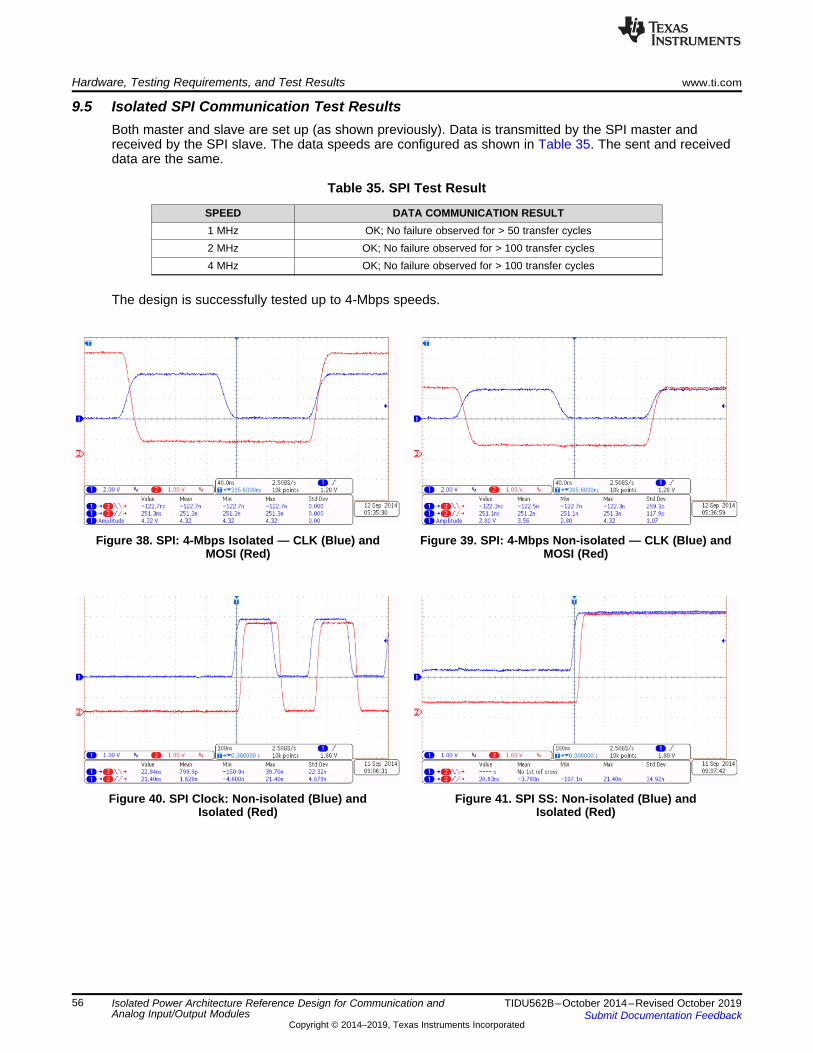
Hardware, Testing Requirements, and Test Results www.ti.com
56 TIDU562B–October 2014–Revised October 2019Submit Documentation Feedback
Copyright © 2014–2019, Texas Instruments Incorporated
Isolated Power Architecture Reference Design for Communication andAnalog Input/Output Modules
9.5 Isolated SPI Communication Test ResultsBoth master and slave are set up (as shown previously). Data is transmitted by the SPI master andreceived by the SPI slave. The data speeds are configured as shown in Table 35. The sent and receiveddata are the same.
Table 35. SPI Test Result
SPEED DATA COMMUNICATION RESULT1 MHz OK; No failure observed for > 50 transfer cycles2 MHz OK; No failure observed for > 100 transfer cycles4 MHz OK; No failure observed for > 100 transfer cycles
The design is successfully tested up to 4-Mbps speeds.
Figure 38. SPI: 4-Mbps Isolated — CLK (Blue) andMOSI (Red)
Figure 39. SPI: 4-Mbps Non-isolated — CLK (Blue) andMOSI (Red)
Figure 40. SPI Clock: Non-isolated (Blue) andIsolated (Red)
Figure 41. SPI SS: Non-isolated (Blue) andIsolated (Red)

www.ti.com Hardware, Testing Requirements, and Test Results
57TIDU562B–October 2014–Revised October 2019Submit Documentation Feedback
Copyright © 2014–2019, Texas Instruments Incorporated
Isolated Power Architecture Reference Design for Communication andAnalog Input/Output Modules
Figure 42. SPI MOSI: Non-isolated (Blue) andIsolated (Red)
Figure 43. SPI MISO: Isolated (Blue) andNon-isolated (Red)
9.6 Isolated I2C CommunicationBoth master and slave are set up (as previously shown). Data is transmitted by the I2C master andreceived by the I2C slave without errors. The clock and data is observed on the oscilloscope. The sentand received data are the same.
Table 36. I2C Test Result
SPEED DATA COMMUNICATION RESULT100 khz OK; No failure observed for > 50 transfer cycles
Figure 44. I2C 100 Kbps: Isolated SCL (Blue) andSDA (Red)
Figure 45. I2C 100 Kbps: Non-isolated SCL (Blue) andSDA (Red)

Hardware, Testing Requirements, and Test Results www.ti.com
58 TIDU562B–October 2014–Revised October 2019Submit Documentation Feedback
Copyright © 2014–2019, Texas Instruments Incorporated
Isolated Power Architecture Reference Design for Communication andAnalog Input/Output Modules
9.7 Summary of Test ResultsThis section summarizes the tests that were performed on the reference design and the observation of thetests
Table 37. Summary of the Tests Performed and Observations
SERIAL NUMBER PARAMETERS OBSERVATION
1 Isolated split-rail supply output with DC/DC configured as Fly-Buck and 24-V input OK
2 Isolated split-rail supply output using isolated DC/DC converter with 5-Vinput OK
3 Isolated 5..4 V, 5 V, 3.7 V, 3.3 V and regulated 5 V and 3.3 V OK
4 Isolated 5 V and 3.3 V using isolated DC/DC power module, transformerdriver and digital isolator with integrated power OK
5 Isolated power supply using a wide-input DC/DC, split-rail DC/DC and dualLDO OK
6 Power supply diagnostics and indication OK
7 Pre-compliance EMI/EMC testing as per CISPR22 and IEC61000-4-4,IEC61000-4-5 OK

www.ti.com Design Files
59TIDU562B–October 2014–Revised October 2019Submit Documentation Feedback
Copyright © 2014–2019, Texas Instruments Incorporated
Isolated Power Architecture Reference Design for Communication andAnalog Input/Output Modules
10 Design Files
10.1 SchematicsTo download the schematics, see the design files at TIDA-00300.
10.2 Bill of MaterialsTo download the bill of materials (BOM) for each board, see the design files at TIDA-00300.
10.3 Layer PlotsTo download the layer plots for each board, see the design files at TIDA-00300.
10.4 Altium ProjectTo download the Altium Designer® project files for each board, see the design files at TIDA-00300.
10.5 Gerber FilesTo download the Gerber files, see the design files at TIDA-00300.
10.6 Assembly DrawingsTo download the assembly drawings, see the design files at TIDA-00300.
11 Related DocumentationTexas Instruments, Digital Isolator Design Guide Developer's Guide
Texas Instruments, Fly-Buck™ converter provides EMC and isolation in PLC applications analogapplications journal
Texas Instruments, Overvoltage Protection for Isolated DC/DC Converter Tech Note
Texas Instruments, How to use isolation to improve ESD, EFT and surge immunity in industrial systemsanalog applications journal
11.1 Related Reference DesignsTexas Instruments, Small Form Factor 12W Ultra Wide Range Power Supply for Protection Relays -Reference Design

About the Author www.ti.com
60 TIDU562B–October 2014–Revised October 2019Submit Documentation Feedback
Copyright © 2014–2019, Texas Instruments Incorporated
Isolated Power Architecture Reference Design for Communication andAnalog Input/Output Modules
11.2 TrademarksE2E, Fly-Buck, NexFET, Tiva, LaunchPad are trademarks of Texas Instruments.Altium Designer is a registered trademark of Altium LLC.Arm, Cortex are registered trademarks of Arm Limited.
12 About the AuthorKALLIKUPPA MUNIYAPPA SREENIVASA is a systems architect at Texas Instruments where he isresponsible for developing reference design solutions for the industrial segment. Sreenivasa brings to thisrole his experience in high-speed digital and analog systems design. Sreenivasa earned his bachelor ofengineering (BE) in electronics and communication engineering (BE-E&C) from VTU, Mysore, India.
PRAHLAD SUPEDA is a systems engineer at Texas Instruments India where he is responsible fordeveloping reference design solutions for the Smart Grid within Industrial Systems. Prahlad Supeda bringsto this role his extensive experience in power electronics, EMC, analog, and mixed signal designs.Prahlad Supeda earned his bachelor of instrumentation and control engineering from Nirma University,India. He can be reached at [email protected].

www.ti.com Revision History
61TIDU562B–October 2014–Revised October 2019Submit Documentation Feedback
Copyright © 2014–2019, Texas Instruments Incorporated
Revision History
Revision HistoryNOTE: Page numbers for previous revisions may differ from page numbers in the current version.
Changes from A Revision (June 2019) to B Revision .................................................................................................... Page
• Changed the Description section........................................................................................................ 1• Changed the products in the Resources section...................................................................................... 1• Changed the Features section .......................................................................................................... 1• Added Isolated DC-DC Converter UCC12050 Advantages section ................................................................ 6• Changed information in System Specifications for TIDA-00300 table.............................................................. 7• Changed information in Details of Functions and Devices Used for Implementing Power Supplies for Communication
Module table ............................................................................................................................... 8• Added a key requirement for designing the isolated power architecture for protection relay modules ........................ 9• Changed Isolated Power Supply Architecture for Communication Modules image............................................. 10• Added Generation of Isolated 5-V, 5.4-V, 3.3-V, or 3.7-V Supply Using Isolated DC/DC With Protection and Diagnostics
section..................................................................................................................................... 11• Deleted Generation of Regulated DC Supplies With Protection and Diagnostics section ..................................... 11• Added Generation of Isolated 5-V, 5.4-V, 3.3-V, or 3.7-V Supply Using Isolated DC/DC With Protection and Diagnostics
section..................................................................................................................................... 13• Added design functionality to Isolated 5-V and 3.3-V Supply Generation Using Power Module section .................... 13• Changed design functionality in Isolated 5-V, 3.3-V and ±12-V Supply Generation Using Transformer Driver section ... 14• Added design functionality and information to Generation of Regulated DC Supplies With Protection and Diagnostics
section..................................................................................................................................... 17• Added information to Isolated Power Supply for Communication Connection Details and Measurements table ........... 48• Added Testing Isolated DC/DC Converter Functional Modes section ............................................................ 48• Added Additional Isolated DC/DC Converter Testing section...................................................................... 49• Added Testing Protection section ..................................................................................................... 49• Changed information in EVMs Used for Isolated Interface Testing and Observations table .................................. 54• Changed information in Summary of the Tests Performed and Observations table............................................ 58
Changes from Original (October 2014) to A Revision .................................................................................................... Page
• Changed the Description section........................................................................................................ 1• Changed the products in the Resources section...................................................................................... 1• Changed the Features section .......................................................................................................... 1• Changed the Applications section....................................................................................................... 1• Added a paragraph to the Design Features section. ................................................................................. 7• Added the TI Device Mapping to Reference Design Functionalities section. ..................................................... 8• Added the System Overview section. .................................................................................................. 9• Added ISO7741 to the Serial Peripheral Interface (SPI) section. ................................................................. 21• Added a NOTE after the ISO7141CC Critical Parameters table................................................................... 34• Added content and several sections to the Hardware, Testing Requirements, and Test Results section. .................. 47

IMPORTANT NOTICE AND DISCLAIMER
TI PROVIDES TECHNICAL AND RELIABILITY DATA (INCLUDING DATASHEETS), DESIGN RESOURCES (INCLUDING REFERENCEDESIGNS), APPLICATION OR OTHER DESIGN ADVICE, WEB TOOLS, SAFETY INFORMATION, AND OTHER RESOURCES “AS IS”AND WITH ALL FAULTS, AND DISCLAIMS ALL WARRANTIES, EXPRESS AND IMPLIED, INCLUDING WITHOUT LIMITATION ANYIMPLIED WARRANTIES OF MERCHANTABILITY, FITNESS FOR A PARTICULAR PURPOSE OR NON-INFRINGEMENT OF THIRDPARTY INTELLECTUAL PROPERTY RIGHTS.These resources are intended for skilled developers designing with TI products. You are solely responsible for (1) selecting the appropriateTI products for your application, (2) designing, validating and testing your application, and (3) ensuring your application meets applicablestandards, and any other safety, security, or other requirements. These resources are subject to change without notice. TI grants youpermission to use these resources only for development of an application that uses the TI products described in the resource. Otherreproduction and display of these resources is prohibited. No license is granted to any other TI intellectual property right or to any thirdparty intellectual property right. TI disclaims responsibility for, and you will fully indemnify TI and its representatives against, any claims,damages, costs, losses, and liabilities arising out of your use of these resources.TI’s products are provided subject to TI’s Terms of Sale (www.ti.com/legal/termsofsale.html) or other applicable terms available either onti.com or provided in conjunction with such TI products. TI’s provision of these resources does not expand or otherwise alter TI’s applicablewarranties or warranty disclaimers for TI products.
Mailing Address: Texas Instruments, Post Office Box 655303, Dallas, Texas 75265Copyright © 2019, Texas Instruments Incorporated