iso14443 type-b contactless coupler chip with anti
TRANSCRIPT

March 2010 Doc ID 11922 Rev 2 1/47
1
CR14ISO14443 type-B contactless coupler chip
with anti-collision and CRC management
Features■ Single 5 V ±500 mV supply voltage
■ SO16N package
■ Contactless communication– ISO14443 type-B protocol– 13.56MHz carrier frequency using an
external oscillator– 106 Kbit/s data rate– 36-byte input/output frame register– Supports frame answer with/without
SOF/EOF– CRC generation and check– Automated ST anti-collision exchange
■ I²C communication– Two-wire I²C serial interface– Supports 400 kHz protocol– 3 chip enable pins– Up to 8 CR14 connected on the same bus
SO16 (MQ)150 mils width
16
1
www.st.com

Contents CR14
2/47 Doc ID 11922 Rev 2
Contents
1 Summary description . . . . . . . . . . . . . . . . . . . . . . . . . . . . . . . . . . . . . . . . 6
2 Signal description . . . . . . . . . . . . . . . . . . . . . . . . . . . . . . . . . . . . . . . . . . . 9
2.1 Oscillator (OSC1, OSC2) . . . . . . . . . . . . . . . . . . . . . . . . . . . . . . . . . . . . . . 9
2.2 Antenna output driver (RFOUT) . . . . . . . . . . . . . . . . . . . . . . . . . . . . . . . . . . 9
2.3 Antenna input filter (RFIN) . . . . . . . . . . . . . . . . . . . . . . . . . . . . . . . . . . . . . 9
2.4 Transmitter reference voltage (VREF) . . . . . . . . . . . . . . . . . . . . . . . . . . . . . 9
2.5 Serial clock (SCL) . . . . . . . . . . . . . . . . . . . . . . . . . . . . . . . . . . . . . . . . . . . . 9
2.6 Serial data (SDA) . . . . . . . . . . . . . . . . . . . . . . . . . . . . . . . . . . . . . . . . . . . 10
2.7 Chip enable (E0, E1, E2) . . . . . . . . . . . . . . . . . . . . . . . . . . . . . . . . . . . . . 10
2.8 Power supply (VCC, GND, GND_RF) . . . . . . . . . . . . . . . . . . . . . . . . . . . . 10
3 CR14 registers . . . . . . . . . . . . . . . . . . . . . . . . . . . . . . . . . . . . . . . . . . . . . 12
3.1 Parameter register (00h) . . . . . . . . . . . . . . . . . . . . . . . . . . . . . . . . . . . . . 12
3.2 Input/Output Frame Register (01h) . . . . . . . . . . . . . . . . . . . . . . . . . . . . . . 13
3.3 Slot marker register (03h) . . . . . . . . . . . . . . . . . . . . . . . . . . . . . . . . . . . . . 14
4 CR14 I²C protocol description . . . . . . . . . . . . . . . . . . . . . . . . . . . . . . . . 16
4.1 I²C start condition . . . . . . . . . . . . . . . . . . . . . . . . . . . . . . . . . . . . . . . . . . . 16
4.2 I²C stop condition . . . . . . . . . . . . . . . . . . . . . . . . . . . . . . . . . . . . . . . . . . . 17
4.3 I²C acknowledge bit (ACK) . . . . . . . . . . . . . . . . . . . . . . . . . . . . . . . . . . . . 17
4.4 I²C data input . . . . . . . . . . . . . . . . . . . . . . . . . . . . . . . . . . . . . . . . . . . . . . 17
4.5 I²C memory addressing . . . . . . . . . . . . . . . . . . . . . . . . . . . . . . . . . . . . . . 18
4.6 CR14 I²C write operations . . . . . . . . . . . . . . . . . . . . . . . . . . . . . . . . . . . . 19
4.7 CR14 I²C read operations . . . . . . . . . . . . . . . . . . . . . . . . . . . . . . . . . . . . 20
5 Applying the I²C protocol to the CR14 registers . . . . . . . . . . . . . . . . . 22
5.1 I²C parameter register protocol . . . . . . . . . . . . . . . . . . . . . . . . . . . . . . . . 22
5.2 I²C input/output frame register protocol . . . . . . . . . . . . . . . . . . . . . . . . . . 23
5.3 I²C slot marker register protocol . . . . . . . . . . . . . . . . . . . . . . . . . . . . . . . . 24
5.4 Addresses above location 06h . . . . . . . . . . . . . . . . . . . . . . . . . . . . . . . . . 25
CR14 Contents
Doc ID 11922 Rev 2 3/47
6 CR14 ISO14443 type-B radio frequency data transfer . . . . . . . . . . . . . 26
6.1 Output RF data transfer from the CR14 to the PICC (request frame) . . . 26
6.2 Transmission format of request frame characters . . . . . . . . . . . . . . . . . . 26
6.3 Request start of frame . . . . . . . . . . . . . . . . . . . . . . . . . . . . . . . . . . . . . . . 27
6.4 Request end of frame . . . . . . . . . . . . . . . . . . . . . . . . . . . . . . . . . . . . . . . . 27
6.5 Input RF data transfer from the PICC to the CR14 (answer frame) . . . . . 28
6.6 Transmission format of answer frame characters . . . . . . . . . . . . . . . . . . . 28
6.7 Answer start of frame . . . . . . . . . . . . . . . . . . . . . . . . . . . . . . . . . . . . . . . . 29
6.8 Answer end of frame . . . . . . . . . . . . . . . . . . . . . . . . . . . . . . . . . . . . . . . . 29
6.9 Transmission frame . . . . . . . . . . . . . . . . . . . . . . . . . . . . . . . . . . . . . . . . . 29
6.10 CRC . . . . . . . . . . . . . . . . . . . . . . . . . . . . . . . . . . . . . . . . . . . . . . . . . . . . . 30
7 Tag access using the CR14 coupler . . . . . . . . . . . . . . . . . . . . . . . . . . . 31
7.1 Standard TAG command access description . . . . . . . . . . . . . . . . . . . . . . 31
7.2 Anti-collision TAG sequence . . . . . . . . . . . . . . . . . . . . . . . . . . . . . . . . . . . 32
8 Maximum rating . . . . . . . . . . . . . . . . . . . . . . . . . . . . . . . . . . . . . . . . . . . . 35
9 DC and AC parameters . . . . . . . . . . . . . . . . . . . . . . . . . . . . . . . . . . . . . . 36
10 Package mechanical . . . . . . . . . . . . . . . . . . . . . . . . . . . . . . . . . . . . . . . . 41
11 Ordering information . . . . . . . . . . . . . . . . . . . . . . . . . . . . . . . . . . . . . . . 43
Appendix A ISO14443 type B CRC calculation . . . . . . . . . . . . . . . . . . . . . . . . . . 44
Revision history . . . . . . . . . . . . . . . . . . . . . . . . . . . . . . . . . . . . . . . . . . . . . . . . . . . . 46
List of tables CR14
4/47 Doc ID 11922 Rev 2
List of tables
Table 1. Signal names . . . . . . . . . . . . . . . . . . . . . . . . . . . . . . . . . . . . . . . . . . . . . . . . . . . . . . . . . . . . 7Table 2. CR14 control registers . . . . . . . . . . . . . . . . . . . . . . . . . . . . . . . . . . . . . . . . . . . . . . . . . . . . 12Table 3. Parameter register bits description . . . . . . . . . . . . . . . . . . . . . . . . . . . . . . . . . . . . . . . . . . . 12Table 4. Input/output frame register description . . . . . . . . . . . . . . . . . . . . . . . . . . . . . . . . . . . . . . . . 14Table 5. Slot marker register description . . . . . . . . . . . . . . . . . . . . . . . . . . . . . . . . . . . . . . . . . . . . . 14Table 6. Device select code . . . . . . . . . . . . . . . . . . . . . . . . . . . . . . . . . . . . . . . . . . . . . . . . . . . . . . . 16Table 7. CR14 request frame character format . . . . . . . . . . . . . . . . . . . . . . . . . . . . . . . . . . . . . . . . 27Table 8. Absolute maximum ratings . . . . . . . . . . . . . . . . . . . . . . . . . . . . . . . . . . . . . . . . . . . . . . . . . 35Table 9. I²C AC measurement conditions. . . . . . . . . . . . . . . . . . . . . . . . . . . . . . . . . . . . . . . . . . . . . 36Table 10. I²C Input Parameters(1,2) . . . . . . . . . . . . . . . . . . . . . . . . . . . . . . . . . . . . . . . . . . . . . . . . . . 36Table 11. I²C DC characteristics . . . . . . . . . . . . . . . . . . . . . . . . . . . . . . . . . . . . . . . . . . . . . . . . . . . . . 36Table 12. I²C AC characteristics . . . . . . . . . . . . . . . . . . . . . . . . . . . . . . . . . . . . . . . . . . . . . . . . . . . . . 38Table 13. RFOUT AC characteristics . . . . . . . . . . . . . . . . . . . . . . . . . . . . . . . . . . . . . . . . . . . . . . . . . . 39Table 14. RFIN AC characteristics . . . . . . . . . . . . . . . . . . . . . . . . . . . . . . . . . . . . . . . . . . . . . . . . . . . 40Table 15. SO16 narrow - 16 lead plastic small outline, 150 mils body width,
package mechanical data . . . . . . . . . . . . . . . . . . . . . . . . . . . . . . . . . . . . . . . . . . . . . . . . . . 42Table 16. Ordering information scheme . . . . . . . . . . . . . . . . . . . . . . . . . . . . . . . . . . . . . . . . . . . . . . . 43Table 17. Document revision history . . . . . . . . . . . . . . . . . . . . . . . . . . . . . . . . . . . . . . . . . . . . . . . . . 46

CR14 List of figures
Doc ID 11922 Rev 2 5/47
List of figures
Figure 1. Logic diagram . . . . . . . . . . . . . . . . . . . . . . . . . . . . . . . . . . . . . . . . . . . . . . . . . . . . . . . . . . . . 7Figure 2. Logic block diagram . . . . . . . . . . . . . . . . . . . . . . . . . . . . . . . . . . . . . . . . . . . . . . . . . . . . . . . 8Figure 3. SO pin connections. . . . . . . . . . . . . . . . . . . . . . . . . . . . . . . . . . . . . . . . . . . . . . . . . . . . . . . . 8Figure 4. CR14 application schematic . . . . . . . . . . . . . . . . . . . . . . . . . . . . . . . . . . . . . . . . . . . . . . . . 10Figure 5. Maximum RL value versus bus capacitance (CBUS) for an I²C bus . . . . . . . . . . . . . . . . . . 11Figure 6. I²C bus protocol . . . . . . . . . . . . . . . . . . . . . . . . . . . . . . . . . . . . . . . . . . . . . . . . . . . . . . . . . 18Figure 7. CR14 I²C write mode sequence . . . . . . . . . . . . . . . . . . . . . . . . . . . . . . . . . . . . . . . . . . . . . 19Figure 8. I²C polling flowchart using ACK . . . . . . . . . . . . . . . . . . . . . . . . . . . . . . . . . . . . . . . . . . . . . 20Figure 9. CR14 I²C read modes sequences . . . . . . . . . . . . . . . . . . . . . . . . . . . . . . . . . . . . . . . . . . . 21Figure 10. Host-to-CR14 transfer: I²C write to parameter register . . . . . . . . . . . . . . . . . . . . . . . . . . . 22Figure 11. CR14-to-host transfer: I²C random address read from parameter register . . . . . . . . . . . . 22Figure 12. CR14-to-host transfer: I²C current address read from parameter register . . . . . . . . . . . . . 22Figure 13. Host-to-CR14 transfer: I²C write to I/O frame register for ISO14443B . . . . . . . . . . . . . . . . 23Figure 14. CR14-to-host transfer: I²C random address read from I/O frame register for ISO14443B 23Figure 15. CR14-to-host transfer: I²C current address read from I/O frame register for ISO14443B . 24Figure 16. Host-to-CR14 transfer: I²C write to slot marker register . . . . . . . . . . . . . . . . . . . . . . . . . . . 24Figure 17. CR14-to-host transfer: I²C random address read from slot marker register . . . . . . . . . . . 24Figure 18. CR14-to-host transfer: I²C current address read from slot marker register . . . . . . . . . . . . 25Figure 19. Wave transmitted using ASK modulation . . . . . . . . . . . . . . . . . . . . . . . . . . . . . . . . . . . . . 26Figure 20. CR14 request frame character format . . . . . . . . . . . . . . . . . . . . . . . . . . . . . . . . . . . . . . . . 27Figure 21. Request start of frame . . . . . . . . . . . . . . . . . . . . . . . . . . . . . . . . . . . . . . . . . . . . . . . . . . . . 27Figure 22. Request end of frame . . . . . . . . . . . . . . . . . . . . . . . . . . . . . . . . . . . . . . . . . . . . . . . . . . . . 27Figure 23. Wave received using BPSK sub-carrier modulation . . . . . . . . . . . . . . . . . . . . . . . . . . . . . 28Figure 24. Answer start of frame . . . . . . . . . . . . . . . . . . . . . . . . . . . . . . . . . . . . . . . . . . . . . . . . . . . . . 29Figure 25. Answer end of frame . . . . . . . . . . . . . . . . . . . . . . . . . . . . . . . . . . . . . . . . . . . . . . . . . . . . . 29Figure 26. Example of a complete transmission frame . . . . . . . . . . . . . . . . . . . . . . . . . . . . . . . . . . . . 30Figure 27. CRC transmission rules . . . . . . . . . . . . . . . . . . . . . . . . . . . . . . . . . . . . . . . . . . . . . . . . . . . 30Figure 28. Standard TAG command: request frame transmission. . . . . . . . . . . . . . . . . . . . . . . . . . . . 31Figure 29. Standard TAG command: answer frame reception . . . . . . . . . . . . . . . . . . . . . . . . . . . . . . 32Figure 30. Standard TAG command: complete TAG access description. . . . . . . . . . . . . . . . . . . . . . . 32Figure 31. Anti-collision ST short range memory sequence (1) . . . . . . . . . . . . . . . . . . . . . . . . . . . . . . 33Figure 32. Anti-collision ST short range memory sequence continued . . . . . . . . . . . . . . . . . . . . . . . . 34Figure 33. I²C AC testing I/O waveform . . . . . . . . . . . . . . . . . . . . . . . . . . . . . . . . . . . . . . . . . . . . . . . . 36Figure 34. I²C AC waveforms. . . . . . . . . . . . . . . . . . . . . . . . . . . . . . . . . . . . . . . . . . . . . . . . . . . . . . . . 37Figure 35. CR14 synchronous timing . . . . . . . . . . . . . . . . . . . . . . . . . . . . . . . . . . . . . . . . . . . . . . . . . 39Figure 36. SO16 narrow - 16 lead plastic small outline, 150 mils body width, Package outline . . . . . 42

Summary description CR14
6/47 Doc ID 11922 Rev 2
1 Summary description
The CR14 is a contactless coupler that is compliant with the short range ISO14443 type-B standard. It is controlled using the two wire I²C bus.
The CR14 generates a 13.56 MHz signal on an external antenna. Transmitted data are modulated using Amplitude Shift Keying (ASK). Received data are demodulated from the PICC (Proximity integrated Coupling Card) load variation signal, induced on the antenna, using Bit Phase Shift Keying (BPSK) of a 847kHz sub-carrier. The Transmitted ASK wave is 10% modulated. The Data transfer rate between the CR14 and the PICC is 106 Kbit/s in both transmission and reception modes.
The CR14 follows the ISO14443 type-B recommendation for Radio frequency power and signal interface.
The CR14 is specifically designed for short range applications that need disposable and reusable products. The CR14 includes an automated anti-collision mechanism that allows it to detect and select any ST short range memories that are present at the same time within its range. The anti-collision mechanism is based on the STMicroelectronics probabilistic scanning method. The CR14 provides a complete analog interface, compliant with the ISO14443 type-B recommendations for Radio-Frequency power and signal interfacing. With it, any ISO14443 type-B PICC products can be powered and have their data transmission controlled via a simple antenna.
The CR14 is fabricated in STMicroelectronics High Endurance Single Poly-silicon CMOS technology.
The CR14 is organized as 4 different blocks (see Figure 2):
● The I²C bus controller. It handles the serial connection with the application host. It is compliant with the 400kHz I²C bus specification, and controls the read/write access to all the CR14 registers.
● The RAM buffer. It is bi-directional. . It stores all the request frame Bytes to be transmitted to the PICC, and all the received Bytes sent by the PICC on the answer frame.
● The transmitter. It powers the PICCs by generating a 13.56MHz signal on an external antenna. The resulting field is 10% modulated using ASK (amplitude shift keying) for outgoing data.
● The receiver. It demodulates the signal generated on the antenna by the load variation of the PICC. The resulting signal is decoded by a 847kHz BPSK (binary phase shift keying) sub-carrier decoder.
The CR14 is designed to be connected to a digital host (Microcontroller or ASIC). This host has to manage the entire communication protocol in both transmit and receive modes, through the I²C serial bus.
CR14 Summary description
Doc ID 11922 Rev 2 7/47
Figure 1. Logic diagram
Table 1. Signal names
Signal Description
RFOUT Antenna Output Driver
RFIN Antenna Input Filter
OSC1 Oscillator Input
OSC2 Oscillator Output
E0, E1, E2 Chip Enable Inputs
SDA I²C Bi-Directional Data
SCL I²C Clock
VCC Power Supply
GND Ground
VREF Transmitter Reference Voltage
GND_RF Ground for RF circuitry
ai12059
RFOUT
CR14
RFIN
OSC1
SCLSDA
E0E1E2
GND GND_RF
VCC VREF
Antenna
OSC2
Summary description CR14
8/47 Doc ID 11922 Rev 2
Figure 2. Logic block diagram
Figure 3. SO pin connections
AI12060
RFOUTCR14
RFIN
OSC1
SCLSDA
E0E1E2
GND GND_RF
VCC VREF
AntennaTran
smitt
erR
ecei
ver
I²C
Bus
Con
trol
ler
RA
M B
uffe
r
OSC2
1
AI10911
234
16151413
GND
E1OSC2OSC1
RFIN
VREF
GND_RFE0
SO16
5678
121110
9 SDAGNDSCL
GND_RFE2
GND
RFOUT
VCC

CR14 Signal description
Doc ID 11922 Rev 2 9/47
2 Signal description
See Figure 1: Logic diagram, and Table 1: Signal names, for an overview of the signals connected to this device.
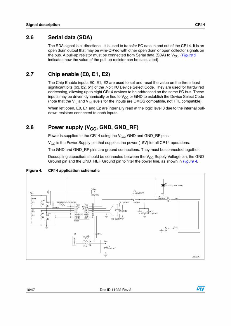
2.1 Oscillator (OSC1, OSC2)The OSC1 and OSC2 pins are internally connected to the on-chip oscillator circuit. The OSC1 pin is the input pin, the OSC2 is the output pin. For correct operation of the CR14, it is required to connect a 13.56MHz quartz crystal across OSC1 and OSC2. If an external clock is used, it must be connected to OSC1 and OSC2 must be left open.
2.2 Antenna output driver (RFOUT)The Antenna Output Driver pin, RFOUT, generates the modulated 13.56MHz signal on the antenna. Care must be taken as it will not withstand a short-circuit.
RFOUT has to be connected to the antenna circuitry as shown in Figure 4: CR14 application schematic The LRC antenna circuitry must be connected across the RFOUT pin and GND.
2.3 Antenna input filter (RFIN)The antenna input filter of the CR14, RFIN, has to be connected to the external antenna through an adapter circuit, as shown in Figure 4.
The input filter demodulates the signal generated on the antenna by the load variation of the PICC. The resulting signal is then decoded by the 847kHz BPSK decoder.
2.4 Transmitter reference voltage (VREF)The Transmitter Reference Voltage input, VREF, provides a reference voltage used by the output driver for ASK modulation.
The Transmitter Reference Voltage input should be connected to an external capacitor, as shown in Figure 4.
2.5 Serial clock (SCL)The SCL input pin is used to strobe all I²C data in and out of the CR14. In applications where this line is used by slave devices to synchronize the bus to a slower clock, the master must have an open drain output, and a pull-up resistor must be connected from the Serial Clock (SCL) to VCC. (Figure 5 indicates how the value of the pull-up resistor can be calculated).
In most applications, though, this method of synchronization is not employed, and so the pull-up resistor is not necessary, provided that the master has a push-pull (rather than open drain) output.
Signal description CR14
10/47 Doc ID 11922 Rev 2
2.6 Serial data (SDA)The SDA signal is bi-directional. It is used to transfer I²C data in and out of the CR14. It is an open drain output that may be wire-OR’ed with other open drain or open collector signals on the bus. A pull-up resistor must be connected from Serial data (SDA) to VCC. (Figure 5 indicates how the value of the pull-up resistor can be calculated).
2.7 Chip enable (E0, E1, E2)The Chip Enable inputs E0, E1, E2 are used to set and reset the value on the three least significant bits (b3, b2, b1) of the 7-bit I²C Device Select Code. They are used for hardwired addressing, allowing up to eight CR14 devices to be addressed on the same I²C bus. These inputs may be driven dynamically or tied to VCC or GND to establish the Device Select Code (note that the VIL and VIH levels for the inputs are CMOS compatible, not TTL compatible).
When left open, E0, E1 and E2 are internally read at the logic level 0 due to the internal pull-down resistors connected to each inputs.
2.8 Power supply (VCC, GND, GND_RF)Power is supplied to the CR14 using the VCC, GND and GND_RF pins.
VCC is the Power Supply pin that supplies the power (+5V) for all CR14 operations.
The GND and GND_RF pins are ground connections. They must be connected together.
Decoupling capacitors should be connected between the VCC Supply Voltage pin, the GND Ground pin and the GND_REF Ground pin to filter the power line, as shown in Figure 4.
Figure 4. CR14 application schematic
VREF 1 RFIN 2 E0 3 E1 4 E2 5 GND_RF 6 GND 7 GND 8 SDA 9 SCL 10 GND 11 OSC2 12OSC1 13 GND_RF 14 RFOUT 15 VCC 16 U1
CR14
X1 13.56MHz
C1 7pF50V
C2 7pF50V
C3 22nF50V
C8100pF50V
C8'8pF50V
C7 120pF50V
C7'33pF50V
VCC
VCC
C6
100nF50V
+ C4 22uF 10V
FL4 0R FL5 0R
FL6 0R
FL7 WURTH 742-792-042
R7 0R
R8
0RR1 OPT ANT1
ANT2
E0 E1
E2
SCL SDA
1 2 3 4 J1
R2 0R
R3 OPT
R4 0R
R5 OPT
R6 0R
VCC
D1 1N4148 (OPTIONAL)
C5 10pF50V
AI12061

CR14 Signal description
Doc ID 11922 Rev 2 11/47
Figure 5. Maximum RL value versus bus capacitance (CBUS) for an I²C bus
AI01665
VCC
CBUS
SDA
RL
MASTER
RL
SCLCBUS
1000
4
8
12
16
20
CBUS (pF)
Max
imum
RP
val
ue (
kΩ)
10 1000
fc = 400kHz
fc = 100kHz

CR14 registers CR14
12/47 Doc ID 11922 Rev 2
3 CR14 registers
The CR14 chip coupler contains six volatile registers. It is entirely controlled, at both digital and analog level, using the three registers listed below and shown in Table 2:
● Parameter Register
● Input/Output Frame Register
● Slot Marker Register
The other 3 registers are located at addresses 02h, 04h and 05h. They are “ST Reserved”, and must not be used in end-user applications.
In the I²C protocol, all data Bytes are transmitted Most Significant Byte first, with each Byte transmitted Most significant bit first.
3.1 Parameter register (00h)The Parameter Register is an 8-bit volatile register used to configure the CR14, and thus, to customize the circuit behavior. The Parameter Register is located at the I²C address 00h and it is accessible in I²C Read and Write modes. Its default value, 00h, puts the CR14 in standard ISO14443 type-B configuration.
Table 2. CR14 control registers
Address Length Access Purpose
00h Parameter Register 1 ByteW Set parameter register
R Read parameter register
01h Input/output Frame Register 36 BytesW
Store and send request frame to the PICC.
Wait for PICC answer frame
R Transfer PICC answered frame data to Host
02h ST Reserved NAW
ST Reserved, must not be used.R
03h Slot Marker Register 1 ByteW
Launch the automated anti-collision process from Slot_0 to Slot_15
R Return data FFh
04h ST Reserved NA R and W ST Reserved. Must not be used
05h ST Reserved NA R and W ST Reserved. Must not be used
Table 3. Parameter register bits description
Bit Control Value Description
b0 Frame Standard0 ISO14443 type-B frame management
1 RFU(1)
b1 RFU 0 Not used
CR14 CR14 registers
Doc ID 11922 Rev 2 13/47
3.2 Input/Output Frame Register (01h)The Input/Output Frame Register is a 36-Byte buffer that is accessed serially from Byte 0 through to Byte 35 (see Table 4). It is located at the I²C address 01h.
The Input/Output Frame Register is the buffer in which the CR14 stores the data Bytes of the request frame to be sent to the PICC. It automatically stores the data Bytes of the answer frame received from the PICC. The first Byte (Byte 0) of the Input/Output Frame Register is used to store the frame length for both transmission and reception.
When accessed in I²C Write mode , the register stores the request frame Bytes that are to be transmitted to the PICC. Byte 0 must be set with the request frame length (in Bytes) and the frame is stored from Byte 1 onwards. At the end of the transmission, the 16-bit CRC is automatically added. After the transmission, the CR14 wait for the PICC to send back an answer frame. When correctly decoded, the PICC answer frame Bytes are stored in the Input/Output Frame Register from Byte 1 onwards. Byte 0 stores the number of Bytes received from the PICC.
When accessed in I²C Read mode, the Input/Output Register sends back the last PICC answer frame Bytes, if any, with Byte 0 transmitted first. The 16-bit CRC is not stored, and it is not sent back on the I²C bus.
The Input/Output Frame Register is set to all 00h between transmission and reception. If there is no answer from the PICC, Byte 0 is set to 00h. In the case of a CRC error, Byte 0 is set to FFh, and the data Bytes are discarded and not appended in the register.
The CR14 Input/Output Frame Register is so designed as to generate all the ST short range memory command frames. It can also generate all standardized ISO14443 type-B command frames like REQB, SLOT-MARKER, ATTRIB, HALT, and get all the answers like ATQB, or answer to ATTRIB. All ISO14443 type-B compliant PICCs can be accessed by the CR14 provided that their data frame exchange is not longer than 35 Bytes in both request and answer.
b2 Answer Frame Format
0 Answer PICC Frames are delimited by SOF and EOF
1Answer PICC Frames do not provide SOF and EOF delimiters
b3 ASK Modulation Depth0 10% ASK modulation depth mode
1 RFU
b4 Carrier Frequency0 13.56MHz carrier on RF OUT is OFF
1 13.56MHz carrier on RF OUT is ON
b5tWDG
Answer delay watchdog
b5=0, b6=0: Watchdog time-out = 500µs to be used for readb5=0, b6=1: Watchdog time-out = 5ms to be used for read
b5=1, b6=0: Watchdog time-out = 10ms to be used for write
b5=1, b6=1: Watchdog time-out = 309ms to be used for MCU timingsb6
b7 RFU 0 Not used
1. RFU = Reserved for Future Use.
Table 3. Parameter register bits description (continued)
Bit Control Value Description

CR14 registers CR14
14/47 Doc ID 11922 Rev 2
3.3 Slot marker register (03h)The slot Marker Register is located at the I²C address 03h. It is used to trigger an automated anti-collision sequence between the CR14 and any ST short range memory present in the electromagnetic field. With one I²C access, the CR14 launches a complete stream of commands starting from PCALL16(), SLOT_MARKER(1), SLOT_MARKER(2) up to SLOT_MARKER(15), and stores all the identified Chip_IDs into the Input/Output Frame Register (I²C address 01h).
This automated anti-collision sequence simplifies the host software development and reduces the time needed to interrogate the 16 slots of the STMicroelectronics anti-collision mechanism.
When accessed in I²C Write mode, the Slot Marker Register starts generating the sequence of anti-collision commands. After each command, the CR14 wait for the ST short range memory answer frame which contains the Chip_ID. The validity of the answer is checked and stored into the corresponding Status Slot Bit (Byte 1 and Byte 2 as described in Table 5). If the answer is correct, the Status Slot Bit is set to ‘1’ and the Chip_ID is stored into the corresponding Slot_Register. If no answer is detected, the Status Slot Bit is set to ‘0’, and the corresponding Slot_Register is set to 00h. If a CRC error is detected, the Status Slot Bit is set to ‘0’, and the corresponding Slot_Register is set to FFh.
Each time the Slot Marker Register is accessed in I²C Write mode, Byte 0 of the Input/Output Frame Register is set to 18, Bytes 1 and 2 provide Status Bits Slot information, and Bytes 3 to 18 store the corresponding Chip_ID or error code.
The Slot Marker Register cannot be accessed in I²C Read mode. All the anti-collision data can be accessed by reading the Input/Output Frame Register at the I²C address 01h.
Table 4. Input/output frame register description
Byte 0 Byte 1 Byte 2 Byte 3 ... Byte 34 Byte 35
Frame Length First data Byte Second data Byte Last data Byte
<------------- Request and Answer Frame Bytes exchanged on the RF ------------->
00h No Byte transmitted
FFh CRC Error
xxh Number of transmitted Bytes
Table 5. Slot marker register description
b7 b6 b5 b4 b3 b2 b1 b0
Byte 0 Number of stored Bytes: fixed to 18
Byte 1Status Slot
Bit 7Status Slot
Bit 6Status Slot
Bit 5Status Slot
Bit 4Status Slot
Bit 3Status Slot
Bit 2Status Slot
Bit 1Status Slot
Bit 0
Byte 2Status Slot
Bit 15Status Slot
Bit 14Status Slot
Bit 13Status Slot
Bit 12Status Slot
Bit 11Status Slot
Bit 10Status Slot
Bit 9Status Slot
Bit 8
Byte 3 Slot_Register 0 = Chip_ID value detected in Slot 0
Byte 4 Slot_Register 1 = Chip_ID value detected in Slot 1
Byte 5 Slot_Register 2 = Chip_ID value detected in Slot 2

CR14 CR14 registers
Doc ID 11922 Rev 2 15/47
Byte 6 Slot_Register 3 = Chip_ID value detected in Slot 3
Byte n .....
Byte 17 Slot_Register 14 = Chip_ID value detected in Slot 14
Byte 18 Slot_Register 15 = Chip_ID value detected in Slot 15
Status bit value description: 1: No error detected. The Chip_ID stored in the Slot register is valid.
0: Error detected
– Slot register = 00h: No answer frame detected from ST short range memory– Slot register = FFh: Answer Frame detected with CRC error. Collision may have occurred
Table 5. Slot marker register description (continued)
b7 b6 b5 b4 b3 b2 b1 b0
CR14 I²C protocol description CR14
16/47 Doc ID 11922 Rev 2
4 CR14 I²C protocol description
The CR14 is compatible with the I²C serial bus memory standard, which is a two-wire serial interface that uses a bi-directional data bus and serial clock.
The CR14 has a pre-programmed, 4-bit identification code, ’1010’ (as shown in Table 6), that corresponds to the I²C bus definition. With this code and the three Chip Enable inputs (E2, E1, E0) up to eight CR14 devices can be connected to the I²C bus, and selected individually.
The CR14 behaves as a slave device in the I²C protocol, with all CR14 operations synchronized to the serial clock.
I²C Read and Write operations are initiated by a START condition, generated by the bus master.
The START condition is followed by the Device Select Code and by a Read/Write bit (R/W). It is terminated by an acknowledge bit. The Device Select Code consists of seven bits (as shown in Table 6):
● the Device Code (first four bits)
● plus three bits corresponding to the states of the three Chip Enable inputs, E2, E1 and E0, respectively
When data is written to the CR14, the device inserts an acknowledge bit (9th bit) after the bus master’s 8-bit transmission.
When the bus master reads data, it also acknowledges the receipt of the data Byte by inserting an acknowledge bit (9th bit).
Data transfers are terminated by a STOP condition after an ACK for Write, or after a NoACK for Read.
The CR14 supports the I²C protocol, as summarized in Figure 6.
Any device that sends data on to the bus, is defined as a transmitter, and any device that reads the data, as a receiver.
The device that controls the data transfer is known as the master, and the other, as the slave. A data transfer can only be initiated by the master, which also provides the serial clock for synchronization. The CR14 is always a slave device in all I²C communications. All data are transmitted Most Significant Bit (MSB) first.
4.1 I²C start conditionSTART is identified by a High-to-Low transition of the Serial Data line, SDA, while the Serial Clock, SCL, is stable in the High state. A START condition must precede any data transfer command.
Table 6. Device select code
Device code Chip enable RW
b7 b6 b5 b4 b3 b2 b1 b0
CR14 Select 1 0 1 0 E2 E1 E0 RW

CR14 CR14 I²C protocol description
Doc ID 11922 Rev 2 17/47
The CR14 continuously monitors the SDA and SCL lines for a START condition (except during Radio Frequency data exchanges), and will not respond unless one is sent.
4.2 I²C stop conditionSTOP is identified by a Low-to-High transition of the Serial Data line, SDA, while the Serial Clock, SCL, is stable in the High state.
A STOP condition terminates communications between the CR14 and the bus master.
A STOP condition at the end of an I²C Read command, after (and only after) a NoACK, forces the CR14 into its stand-by state.
A STOP condition at the end of an I²C Write command triggers the Radio Frequency data exchange between the CR14 and the PICC.
4.3 I²C acknowledge bit (ACK)An acknowledge bit is used to indicate a successful data transfer on the I²C bus.
The bus transmitter, either master or slave, releases the Serial Data line, SDA, after sending 8 bits of data. During the 9th clock pulse the receiver pulls the SDA line Low to acknowledge the receipt of the 8 data bits.
4.4 I²C data inputDuring data input, the CR14 samples the SDA bus signal on the rising edge of the Serial Clock, SCL. For correct device operation, the SDA signal must be stable during the Low-to-High Serial Clock transition, and the data must change only when the SCL line is Low.

CR14 I²C protocol description CR14
18/47 Doc ID 11922 Rev 2
Figure 6. I²C bus protocol
4.5 I²C memory addressingTo start up communication with the CR14, the bus master must initiate a START condition. Then, the bus master sends 8 bits (with the most significant bit first) on the Serial Data line, SDA. These bits consist of the Device Select Code (7 bits) plus a RW bit.
According to the I²C bus definition, the seven most significant bits of the Device Select Code are the Device Type Identifier. For the CR14, these bits are defined as shown in Table 6.
The 8th bit is the Read/Write bit (RW). It is set to ‘1’ for I²C Read, and to ‘0’ for I²C Write operations.
If the data sent by the bus master matches the Device Select Code of a CR14 device, the corresponding device returns an acknowledgment on the SDA bus during the 9th bit time.
The CR14 devices whose Device Select Codes do not correspond to the data sent, generate a No-ACK. They deselect themselves from the bus and go into stand-by mode.
SCL
SDA
SCL
SDA
SDA
STARTCONDITION
SDAINPUT
SDACHANGE
AI00792
STOPCONDITION
1 2 3 7 8 9
MSB ACK
STARTCONDITION
SCL 1 2 3 7 8 9
MSB ACK
STOPCONDITION

CR14 CR14 I²C protocol description
Doc ID 11922 Rev 2 19/47
4.6 CR14 I²C write operationsThe bus master sends a START condition, followed by a Device Select Code and the R/W bit set to ’0’. The CR14 that corresponds to the Device Select Code, acknowledges and waits for the bus master to send the Byte address of the register that is to be written to. After receipt of the address, the CR14 returns another ACK, and waits for the bus master to send the data Bytes that are to be written.
In the CR14 I²C Write mode, the bus master may sends one or more data Bytes depending on the selected register.
The CR14 replies with an ACK after each data Byte received. The bus master terminates the transfer by generating a STOP condition.
The STOP condition at the end of a Write access to the Input/Output Frame Register causes the Radio Frequency data exchange between the CR14 and the PICC to be started.
During the Radio Frequency data exchange, the CR14 disconnects itself from the I²C bus. The time (tRFEX) needed to complete the exchange is not fixed as it depends on the PICC command format. To know when the exchange is complete, the bus master uses an ACK polling sequence as shown in Figure 8. It consists of the following:
● Initial condition: a Radio Frequency data exchange is in progress.
● Step 1: the master issues a START condition followed by the first Byte of the new instruction (Device Select Code plus R/W bit).
● Step 2: if the CR14 is busy, no ACK is returned and the master goes back to Step 1. If the CR14 has completed the Radio Frequency data exchange, it responds with an ACK, indicating that it is ready to receive the second part of the next instruction (the first Byte of this instruction being sent during Step 1).
Figure 7. CR14 I²C write mode sequence
AI12062
STO
P
DATA N
ACK ACK
STA
RT
CR14 WRITE
DEV SEL BYTE ADDR DATA 1 DATA 2 DATA 3
ACK ACK ACK ACK
R/W
BUS Master
BUS Slave

CR14 I²C protocol description CR14
20/47 Doc ID 11922 Rev 2
Figure 8. I²C polling flowchart using ACK
4.7 CR14 I²C read operationsTo send a Read command, the bus master sends a START condition, followed by a Device Select Code and the R/W bit set to ’1’.
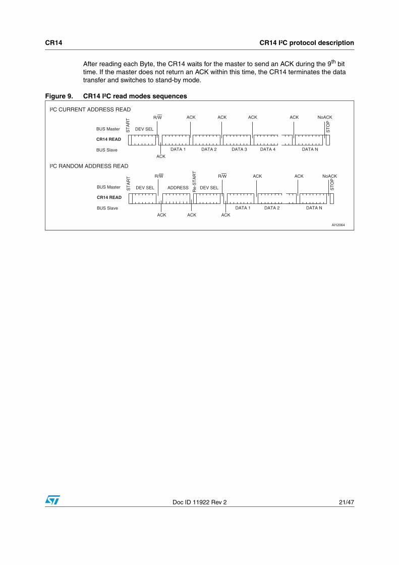
The CR14 that corresponds to the Device Select Code acknowledges and outputs the first data Byte of the addressed register.
To select a specific register, a dummy Write command must first be issued, giving an address Byte but no data Bytes, as shown in the bottom half of Figure 9. This causes the new address to be stored in the internal address pointer, for use by the Read command that immediately follows the dummy Write command.
In the I²C Read mode, the CR14 may read one or more data Bytes depending on the selected register. The bus master has to generate an ACK after each data Byte to read all the register data in a continuous stream. Only the last data Byte should not be followed by an ACK. The master then terminates the transfer with a STOP condition, as shown in Figure 9.
Radio Frequencydata exchange
in progress
START Condition
DEVICE SELECTCODE with R/W=1
ACKreturned
Nextoperation isaddressingthe CR14
ReSTART
STOPSTOP
Proceed to READOperation
YES
NO
First byte of instructionwith R/W = 1 alreadydecoded by the CR14
NO YES
ai12063
CR14 CR14 I²C protocol description
Doc ID 11922 Rev 2 21/47
After reading each Byte, the CR14 waits for the master to send an ACK during the 9th bit time. If the master does not return an ACK within this time, the CR14 terminates the data transfer and switches to stand-by mode.
Figure 9. CR14 I²C read modes sequences
ST
AR
T
CR14 READ
DEV SEL
DATA 1 DATA 2 DATA 3
AI12064
ST
OP
DATA N
ACK
ACK ACKR/W ACK NoACK
BUS Master
BUS Slave
ACK
DATA 4
ST
AR
T
CR14 READ
DEV SEL ADDRESS
ACK
BUS Master
BUS Slave
R/W
ACK
DEV SEL
DATA 1
ST
OP
DATA N
ACK
ACKR/W ACK NoACK
DATA 2
Re-
ST
AR
T
I²C CURRENT ADDRESS READ
I²C RANDOM ADDRESS READ

Applying the I²C protocol to the CR14 registers CR14
22/47 Doc ID 11922 Rev 2
5 Applying the I²C protocol to the CR14 registers
5.1 I²C parameter register protocolFigure 10 shows how new data is written to the Parameter Register. The new value becomes active after the I²C STOP condition.
Figure 11 shows how to read the Parameter Register contents. The CR14 sends and re-sends the Parameter Register contents until it receives a NoACK from the I²C Host.
The CR14 supports the I²C Current Address and Random Address Read modes. The Current Address Read mode can be used if the previous command was issued to the register where the Read is to take place.
Figure 10. Host-to-CR14 transfer: I²C write to parameter register
Figure 11. CR14-to-host transfer: I²C random address read from parameter register
Figure 12. CR14-to-host transfer: I²C current address read from parameter register
START
1 0 1 0 X X X 00h data
STOP
ACKACKACK
Register ByteValue
Parameter RegisterAddress
Device SelectCode
Bus Master
CR14 Write
Bus Slave
ai12038
R/W
START
1 0 1 0 X X X 00h data
STOP
ACKACKACK
Register ByteValue
Parameter RegisterAddress
Device SelectCode
Bus Master
CR14 Read
Bus Slave
ai12039
RESTART
1 0 1 0 X X X
R/W
Device SelectCode
R/W NoACK
data
STOP
ACK
Register ByteValue
Bus Master
CR14 Read
Bus Slave
ai12040
START
1 0 1 0 X X X
Device SelectCode
R/W NoACK

CR14 Applying the I²C protocol to the CR14 registers
Doc ID 11922 Rev 2 23/47
5.2 I²C input/output frame register protocolFigure 13 shows how to store a PICC request frame command of N Bytes into the Input/Output Frame Register.
After the I²C STOP condition, the request frame is RF transmitted in the ISO14443 type-B format. The CR14 then waits for the PICC answer frame which will also be stored in the Input/Output Frame Register. The request frame is over-written by the answer frame.
Figure 14 shows how to read an N-Byte PICC answer frame.
The two CRC Bytes generated by the PICC are not stored.
The CR14 continues to output data Bytes until a NoACK has been generated by the I²C Host, and received by the CR14. After all 36 Bytes have been output, the CR14 “rolls over”, and starts outputting from the start of the Input/Output Frame Register again.
The CR14 supports the I²C Current Address and Random Address Read modes. The Current Address Read mode can be used if the previous command was issued to the register where the Read is to take place.
Figure 13. Host-to-CR14 transfer: I²C write to I/O frame register for ISO14443B
Figure 14. CR14-to-host transfer: I²C random address read from I/O frame register for ISO14443B
START
1 0 1 0 XX X 01h N
STOP
ACKACKACK
Request FrameLength N
Input/OutputRegisterAddress
DeviceSelectCode
BusMaster
CR14Write
BusSlave
ai12041
R/W
Data 1 Data 2
PICCCommandParameter
PICCCommand
Code
Data N
PICCCommandParameter
PICCCommandParameter
ACKACKACKACK
START
1 0 1 0XXX 01h N
STOP
ACK
ACKACK
ReceivedFrameLength
Input/OutputRegisterAddress
DeviceSelectCode
BusMaster
CR14Read
BusSlave
ai12042
R/W
Data1 Data 2
AnswerFrameData
AnswerFrameData
Data N
AnswerFrameData
AnswerFrameData
NoACKACKACKACKRESTART
1 0 1 0 XXX
DeviceSelectCode
R/W
ACK
Applying the I²C protocol to the CR14 registers CR14
24/47 Doc ID 11922 Rev 2
Figure 15. CR14-to-host transfer: I²C current address read from I/O frame register for ISO14443B
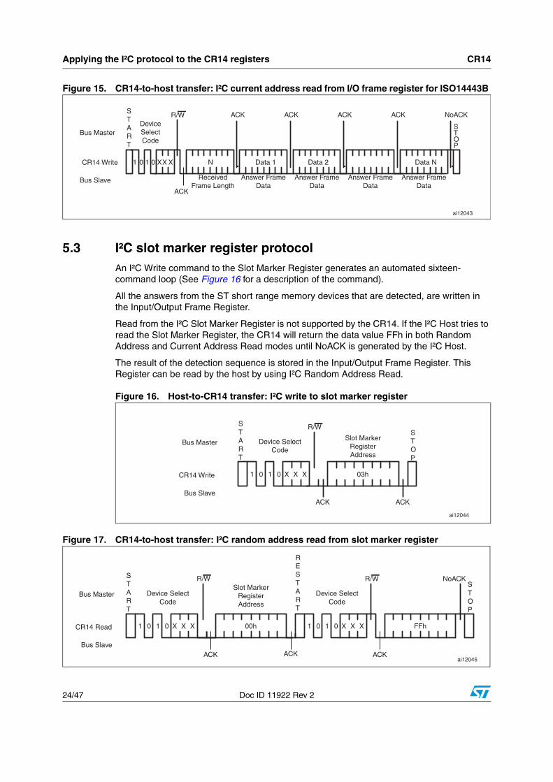
5.3 I²C slot marker register protocolAn I²C Write command to the Slot Marker Register generates an automated sixteen-command loop (See Figure 16 for a description of the command).
All the answers from the ST short range memory devices that are detected, are written in the Input/Output Frame Register.
Read from the I²C Slot Marker Register is not supported by the CR14. If the I²C Host tries to read the Slot Marker Register, the CR14 will return the data value FFh in both Random Address and Current Address Read modes until NoACK is generated by the I²C Host.
The result of the detection sequence is stored in the Input/Output Frame Register. This Register can be read by the host by using I²C Random Address Read.
Figure 16. Host-to-CR14 transfer: I²C write to slot marker register
Figure 17. CR14-to-host transfer: I²C random address read from slot marker register
START
1 0 1 0 XX X N
STOP
ACK
ACK
Answer FrameData
DeviceSelectCode
Bus Master
CR14 Write
Bus Slave
ai12043
R/W
Data 1 Data 2
Answer FrameData
Answer FrameData
Data N
Answer FrameData
ReceivedFrame Length
ACKACK NoACKACK
03h
STOP
ACK
Slot MarkerRegisterAddress
Bus Master
CR14 Write
Bus Slave
ai12044
START
1 0 1 0 X X X
Device SelectCode
R/W
ACK
START
1 0 1 0 X X X 00h FFh
STOP
ACKACKACK
Slot MarkerRegisterAddress
Device SelectCode
Bus Master
CR14 Read
Bus Slave
ai12045
RESTART
1 0 1 0 X X X
R/W
Device SelectCode
R/W NoACK

CR14 Applying the I²C protocol to the CR14 registers
Doc ID 11922 Rev 2 25/47
Figure 18. CR14-to-host transfer: I²C current address read from slot marker register
5.4 Addresses above location 06hIn I²C Write mode, when the CR14 receives the 8-bit register address, and the address is above location 06h, the device does not acknowledge (NoACK) and deselects itself from the bus. The Serial Data line, SDA, stays at logic ‘1’ (pull-up resistor), and the I²C Host receives a NoACK during the 9th bit time. The SDA line stays High until the STOP condition is issued.
In the I²C Current and Random Address Read modes, when the CR14 receives the 8-bit register address, and the address is above location 06h, the device does not acknowledge the Device Select Code after the START condition, and deselects itself from the bus.
FFh
STOP
ACK
Bus Master
CR14 Read
Bus Slave
ai12047
START
1 0 1 0 X X X
Device SelectCode
R/W NoACK

CR14 ISO14443 type-B radio frequency data transfer CR14
26/47 Doc ID 11922 Rev 2
6 CR14 ISO14443 type-B radio frequency data transfer
6.1 Output RF data transfer from the CR14 to the PICC (request frame)The CR14 output buffer is controlled by the 13.56MHz clock signal generated by the external oscillator and by the request frame generator. The CR14 can be directly connected to an external matching circuit to generate a 13.56MHz sinusoidal carrier frequency on its antenna.
The current driven into the antenna coil is directly generated by the CR14 RFOUT output driver.
If the antenna is correctly tuned, it emits an H-field of a large enough magnitude to power a contactless PICC from a short distance. The energy received on the PICC antenna is converted to a Power Supply Voltage by a regulator, and turned into data bits by the ASK demodulator. The CR14 amplitude modulates the 13.56MHz wave by 10% as represented in Figure 19. The data transfer rate is 106 kbit/s.
Figure 19. Wave transmitted using ASK modulation
6.2 Transmission format of request frame characters The CR14 transmits characters of 10 bits, with the Least Significant Bit (b0) transmitted first, as shown in Figure 20.
Several 10-bit characters, preceded by the Start Of Frame (SOF) and followed by the End Of Frame (EOF), constitute a Request Frame, as shown in Figure 26.
A Request Frame includes the SOF, instructions, addresses, data, CRC and the EOF as defined in the ISO14443 type-B.
Each bit duration is called an Elementary Time Unit (ETU). One ETU is equal to 9.44µs (1/106kHz).
DATA BIT TRANSMITTEDBY THE CR14
10% ASK MODULATIONOF THE 13.56MHz WAVE,GENERATED BY THE RFOUTDRIVER
Transfer time for one data bit is 1/106 kHzAI12048
10% ASK MODULATIONOF THE 13.56MHz WAVE,GENERATED ON THE CR14ANTENNA

CR14 CR14 ISO14443 type-B radio frequency data transfer
Doc ID 11922 Rev 2 27/47
Figure 20. CR14 request frame character format
6.3 Request start of frameThe Start Of Frame (SOF) described in Figure 21 consists of:
● a falling edge,
● followed by ten Elementary Time Units (ETU) each containing a logical ‘0’
● followed by a single rising edge
● followed by two ETUs, each containing a logical ‘1’.
Figure 21. Request start of frame
6.4 Request end of frameThe End Of Frame (EOF) shown in Figure 22 consists of:
● a falling edge,
● followed by ten Elementary Time Units (ETU) containing each a logical ‘0’,
● followed by a single rising edge.
Figure 22. Request end of frame
Table 7. CR14 request frame character format
Bit Description Value
b0 Start bit used to synchronize the transmission b0 = 0
b1 to b8 Information Byte (instruction, address or data)Information Byte is sent Least Significant Bit first
b9 Stop bit used to indicate the end of the character b9 = 1
1ETU
Start'0'
LSB MSB Stop'1'
Information Byte
b0 b1 b2 b3 b4 b5 b6 b7 b8 b9
ai12049
b0 b1 b2 b3 b4 b5 b6 b7 b8 b9 b10 b11
ETU 0 0 0 0 0 0 0 0 0 0 1 1
ai12050
b0 b1 b2 b3 b4 b5 b6 b7 b8 b9
ETU 0 0 0 0 0 0 0 0 0 0
ai09252
CR14 ISO14443 type-B radio frequency data transfer CR14
28/47 Doc ID 11922 Rev 2
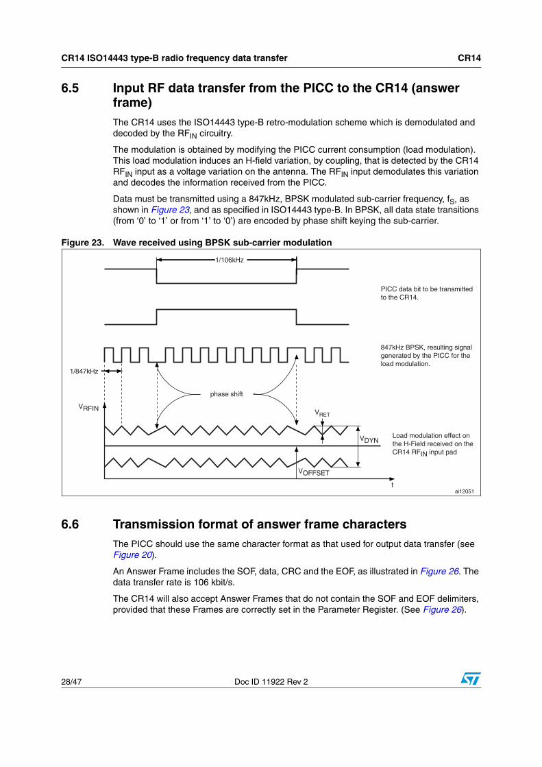
6.5 Input RF data transfer from the PICC to the CR14 (answer frame)The CR14 uses the ISO14443 type-B retro-modulation scheme which is demodulated and decoded by the RFIN circuitry.
The modulation is obtained by modifying the PICC current consumption (load modulation). This load modulation induces an H-field variation, by coupling, that is detected by the CR14 RFIN input as a voltage variation on the antenna. The RFIN input demodulates this variation and decodes the information received from the PICC.
Data must be transmitted using a 847kHz, BPSK modulated sub-carrier frequency, fS, as shown in Figure 23, and as specified in ISO14443 type-B. In BPSK, all data state transitions (from ‘0’ to ‘1’ or from ‘1’ to ‘0’) are encoded by phase shift keying the sub-carrier.
Figure 23. Wave received using BPSK sub-carrier modulation
6.6 Transmission format of answer frame charactersThe PICC should use the same character format as that used for output data transfer (see Figure 20).
An Answer Frame includes the SOF, data, CRC and the EOF, as illustrated in Figure 26. The data transfer rate is 106 kbit/s.
The CR14 will also accept Answer Frames that do not contain the SOF and EOF delimiters, provided that these Frames are correctly set in the Parameter Register. (See Figure 26).
VDYN
VRFIN
t
VOFFSET
1/106kHz
1/847kHz
phase shift
VRET
Load modulation effect onthe H-Field received on theCR14 RFIN input pad
PICC data bit to be transmittedto the CR14.
847kHz BPSK, resulting signalgenerated by the PICC for theload modulation.
ai12051
CR14 CR14 ISO14443 type-B radio frequency data transfer
Doc ID 11922 Rev 2 29/47
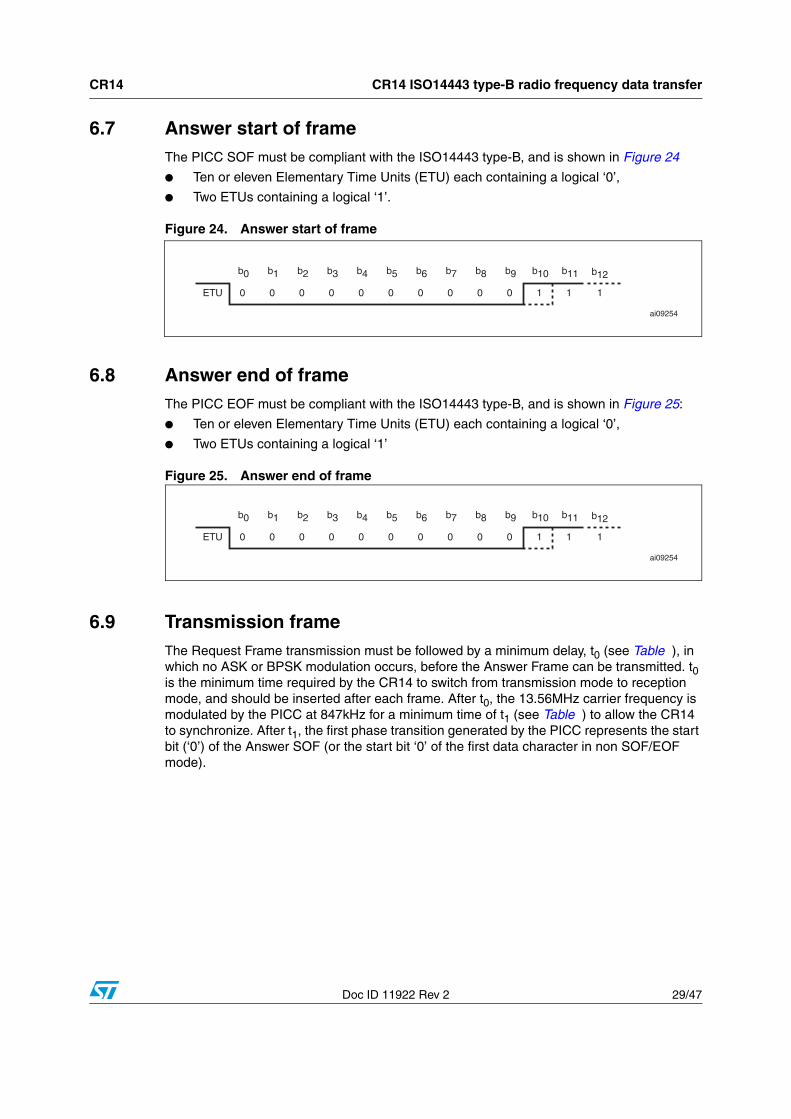
6.7 Answer start of frameThe PICC SOF must be compliant with the ISO14443 type-B, and is shown in Figure 24
● Ten or eleven Elementary Time Units (ETU) each containing a logical ‘0’,
● Two ETUs containing a logical ‘1’.
Figure 24. Answer start of frame
6.8 Answer end of frameThe PICC EOF must be compliant with the ISO14443 type-B, and is shown in Figure 25:
● Ten or eleven Elementary Time Units (ETU) each containing a logical ‘0’,
● Two ETUs containing a logical ‘1’
Figure 25. Answer end of frame
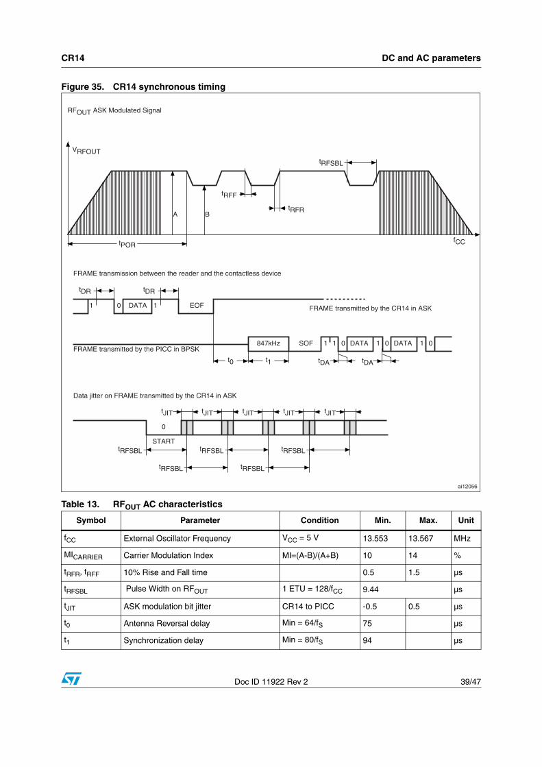
6.9 Transmission frameThe Request Frame transmission must be followed by a minimum delay, t0 (see Table ), in which no ASK or BPSK modulation occurs, before the Answer Frame can be transmitted. t0 is the minimum time required by the CR14 to switch from transmission mode to reception mode, and should be inserted after each frame. After t0, the 13.56MHz carrier frequency is modulated by the PICC at 847kHz for a minimum time of t1 (see Table ) to allow the CR14 to synchronize. After t1, the first phase transition generated by the PICC represents the start bit (‘0’) of the Answer SOF (or the start bit ‘0’ of the first data character in non SOF/EOF mode).
b0 b1 b2 b3 b4 b5 b6 b7 b8 b9 b10 b11
ETU 0 0 0 0 0 0 0 0 0 0 1 1
ai09254
b12
1
b0 b1 b2 b3 b4 b5 b6 b7 b8 b9 b10 b11
ETU 0 0 0 0 0 0 0 0 0 0 1 1
ai09254
b12
1
CR14 ISO14443 type-B radio frequency data transfer CR14
30/47 Doc ID 11922 Rev 2
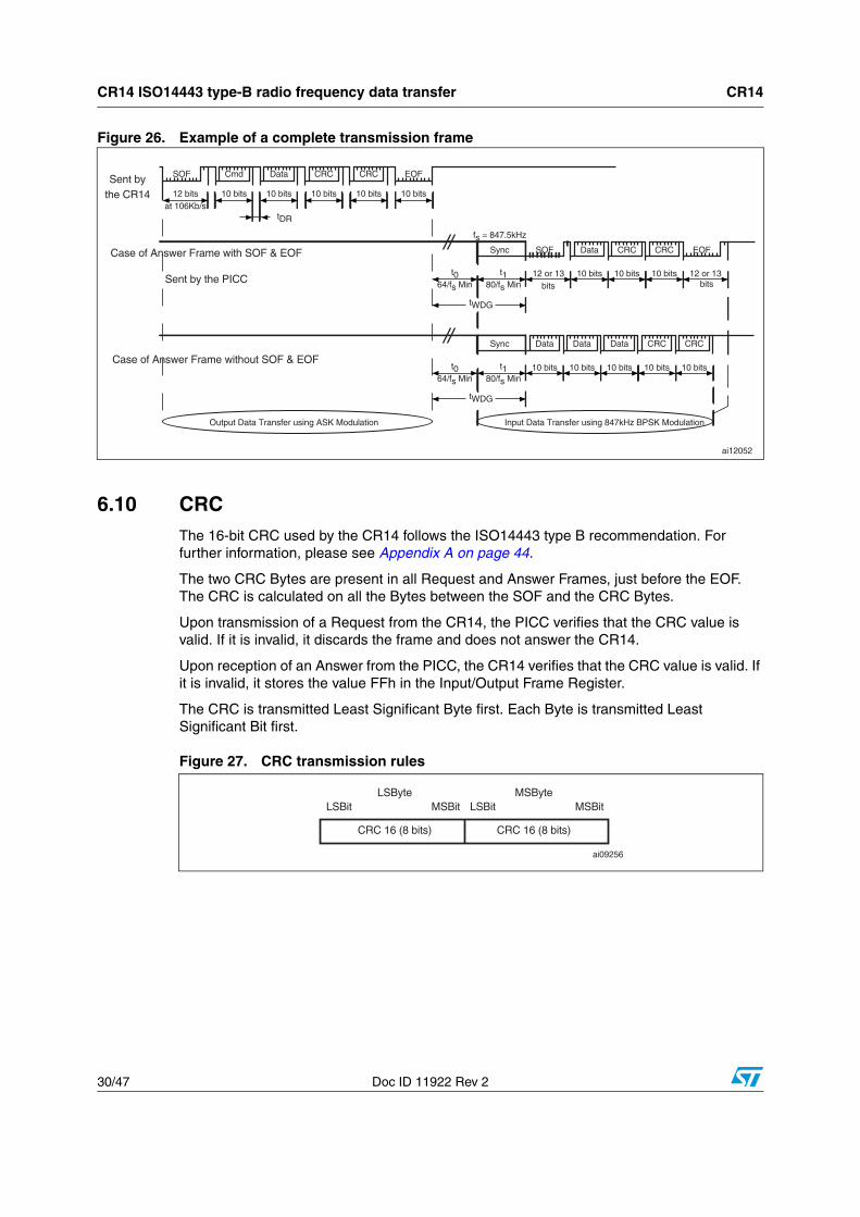
Figure 26. Example of a complete transmission frame
6.10 CRCThe 16-bit CRC used by the CR14 follows the ISO14443 type B recommendation. For further information, please see Appendix A on page 44.
The two CRC Bytes are present in all Request and Answer Frames, just before the EOF. The CRC is calculated on all the Bytes between the SOF and the CRC Bytes.
Upon transmission of a Request from the CR14, the PICC verifies that the CRC value is valid. If it is invalid, it discards the frame and does not answer the CR14.
Upon reception of an Answer from the PICC, the CR14 verifies that the CRC value is valid. If it is invalid, it stores the value FFh in the Input/Output Frame Register.
The CRC is transmitted Least Significant Byte first. Each Byte is transmitted Least Significant Bit first.
Figure 27. CRC transmission rules
SOF Cmd Data CRC CRC EOF
12 bitsat 106Kb/s
10 bits 10 bits10 bits 10 bits 10 bits
Sent bythe CR14
t064/fs Min
t180/fs Min
Sync
fs = 847.5kHz
SOF Data CRC CRC EOF
12 or 13bits
10 bits 12 or 13 bits
10 bits 10 bits
tWDG
Case of Answer Frame with SOF & EOF
Sent by the PICC
Sync Data Data CRC
tWDG
Case of Answer Frame without SOF & EOF
Data CRC
t064/fs Min
t180/fs Min
10 bits 10 bits 10 bits10 bits 10 bits
Output Data Transfer using ASK Modulation Input Data Transfer using 847kHz BPSK Modulation
ai12052
tDR
LSByte MSByte
CRC 16 (8 bits) CRC 16 (8 bits)
LSBit MSBit LSBit MSBit
ai09256

CR14 Tag access using the CR14 coupler
Doc ID 11922 Rev 2 31/47
7 Tag access using the CR14 coupler
In all the following I²C commands, the last three bits of the Device Select Code can be replaced by any of the three-bit binary values (000, 001, 010, 011, 100, 101, 110, 111). These values are linked to the logic levels applied to the E2, E1 and E0 pads of the CR14.
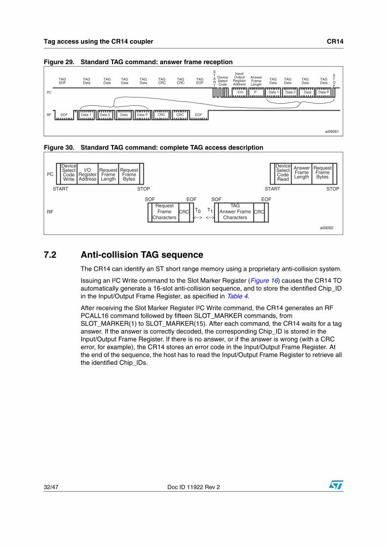
7.1 Standard TAG command access descriptionStandard PICC commands, like Read and Write, are generated by the CR14 using the Input/Output Frame Register.
When the host needs to send a standard frame command to the PICC, it first has to internally generate the complete frame, with the command code followed by the command parameters. Only the two CRC Bytes should not be generated, as the CR14 automatically adds them during the RF transmission.
When the frame is ready, the host has to write the request frame into the Input/Output Frame Register using the I²C write command specified in Figure 13 on page 23. After the I²C STOP condition, the CR14 inserts the I²C Bytes in the required ISO character format ( Figure 20) and starts to transmit the request frame to the PICC. Once the RF transmission is over, the CR14 waits for the PICC to send an answer frame.
If the PICC answers, the characters received (Figure 26) are demodulated, decoded and stored into the Input/Output Frame Register, as specified in Table 4. During the entire RF transmission, the CR14 disconnects itself from the I²C bus. On reception of the PICC EOF, the CR14 checks the CRC and reconnects itself to the I²C bus. The host can then get the PICC answer frame by issuing an Input/Output Frame Register Read on the I²C bus, as specified in Figures 14 and 15.
If no answer from the PICC is detected after a time-out delay, fixed in the Parameter Register (bits b5 and b6), the Input/Output Frame Register is set as specified in Table 4.
Figure 28. Standard TAG command: request frame transmission
START
DeviceSelectCode
Input/Output
RegisterAddress
RequestFrameLength
TAGCmdCode
Param Param Param
STOP
SOF EOFData 1 DataData 2 Data N CRC CRC
CR14SOF
TAGCmdCode
Param Param Param SR14EOFCRC CRC
I²C
RF
ai12053
Data 1 DataData 2 Data N01h N
Tag access using the CR14 coupler CR14
32/47 Doc ID 11922 Rev 2
Figure 29. Standard TAG command: answer frame reception
Figure 30. Standard TAG command: complete TAG access description
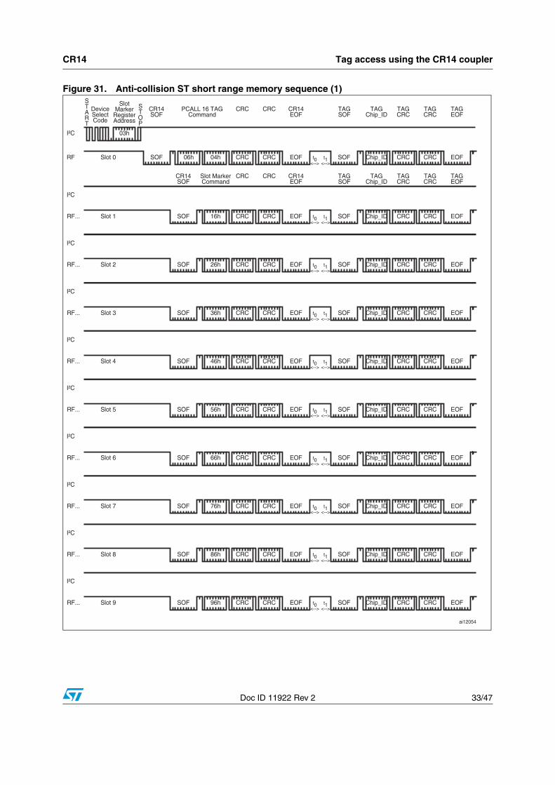
7.2 Anti-collision TAG sequenceThe CR14 can identify an ST short range memory using a proprietary anti-collision system.
Issuing an I²C Write command to the Slot Marker Register (Figure 16) causes the CR14 TO automatically generate a 16-slot anti-collision sequence, and to store the identified Chip_ID in the Input/Output Frame Register, as specified in Table 4.
After receiving the Slot Marker Register I²C Write command, the CR14 generates an RF PCALL16 command followed by fifteen SLOT_MARKER commands, from SLOT_MARKER(1) to SLOT_MARKER(15). After each command, the CR14 waits for a tag answer. If the answer is correctly decoded, the corresponding Chip_ID is stored in the Input/Output Frame Register. If there is no answer, or if the answer is wrong (with a CRC error, for example), the CR14 stores an error code in the Input/Output Frame Register. At the end of the sequence, the host has to read the Input/Output Frame Register to retrieve all the identified Chip_IDs.
START
DeviceSelectCode
Input/Output
RegisterAddress
AnswerFrameLength
TAGData
STOP
SOF EOFData 1 DataData 2 Data P CRC CRC
TAGSOF
TAGData
TAGData
TAGData
TAGData
TAGEOF
TAGCRC
TAGCRC
I²C
RF
ai09261
Data 1 DataData 2 Data P01h P
TAGData
TAGData
TAGData
DeviceSelectCodeWrite
I/ORegisterAddress
RequestFrameLength
RequestFrameBytes
I²C
START STOP
CRCRequestFrame
Characters
SOF EOF
CRCTAG
Answer FrameCharacters
SOF EOF
T0<-->
T1<-->
DeviceSelectCodeRead
AnswerFrameLength
RequestFrameBytes
START STOP
RF
ai09262
CR14 Tag access using the CR14 coupler
Doc ID 11922 Rev 2 33/47
Figure 31. Anti-collision ST short range memory sequence (1)
03hI²C
START
DeviceSelectCode
SlotMarker
RegisterAddress
STOP
SOFSlot 0 06h 04h CRC CRC EOF SOFt0<-->
t1<-->
Chip_ID CRC CRC EOF
CR14SOF
PCALL 16 TAGCommand
CRC CRC CR14EOF
TAGSOF
TAGChip_ID
TAGCRC
TAGCRC
TAGEOF
RF
I²C
SOFSlot 1 16h CRC CRC EOF SOFt0<-->
t1<-->
Chip_ID CRC CRC EOFRF...
I²C
SOFSlot 2 26h CRC CRC EOF SOFt0<-->
t1<-->
Chip_ID CRC CRC EOFRF...
I²C
SOFSlot 3 36h CRC CRC EOF SOFt0<-->
t1<-->
Chip_ID CRC CRC EOFRF...
I²C
SOFSlot 4 46h CRC CRC EOF SOFt0<-->
t1<-->
Chip_ID CRC CRC EOFRF...
I²C
SOFSlot 5 56h CRC CRC EOF SOFt0<-->
t1<-->
Chip_ID CRC CRC EOFRF...
I²C
SOFSlot 6 66h CRC CRC EOF SOFt0<-->
t1<-->
Chip_ID CRC CRC EOFRF...
I²C
SOFSlot 7 76h CRC CRC EOF SOFt0<-->
t1<-->
Chip_ID CRC CRC EOFRF...
I²C
SOFSlot 8 86h CRC CRC EOF SOFt0<-->
t1<-->
Chip_ID CRC CRC EOFRF...
I²C
SOFSlot 9 96h CRC CRC EOF SOFt0<-->
t1<-->
Chip_ID CRC CRC EOFRF...
CR14SOF
Slot MarkerCommand
CRC CRC CR14EOF
TAGSOF
TAGChip_ID
TAGCRC
TAGCRC
TAGEOF
ai12054

Tag access using the CR14 coupler CR14
34/47 Doc ID 11922 Rev 2
Figure 32. Anti-collision ST short range memory sequence continued
I²C
SOFSlot 10 96h CRC CRC EOF SOFt0<-->
t1<-->
Chip_ID CRC CRC EOFRF ...
I²C
SOFSlot 11 56h CRC CRC EOF SOFt0<-->
t1<-->
Chip_ID CRC CRC EOFRF ...
I²C
SOFSlot 12 66h CRC CRC EOF SOFt0<-->
t1<-->
Chip_ID CRC CRC EOFRF ...
I²C
SOFSlot 13 76h CRC CRC EOF SOFt0<-->
t1<-->
Chip_ID CRC CRC EOFRF ...
I²C
SOFSlot 14 86h CRC CRC EOF SOFt0<-->
t1<-->
Chip_ID CRC CRC EOFRF ...
I²C
SOFSlot 15 96h CRC CRC EOF SOFt0<-->
t1<-->
Chip_ID CRC CRC EOFRF ...
01hI²C ...
START
DeviceSelectCode
I/ORegisterAddress
RESTART
DeviceSelectCode
AnswerFrameLength
Slot 0Chip_IDAnswer
Status12h Status Chip_ID Chip_IDChip_ID Chip_ID Chip_ID Chip_IDChip_ID Chip_ID Chip_ID
StatusSlot Bitsb0 to b7
StatusSlot Bitsb8 to b15
Slot 1Chip_IDAnswer
Slot 2Chip_IDAnswer
Slot 3Chip_IDAnswer
Slot 4Chip_IDAnswer
Slot 5Chip_IDAnswer
Slot 6Chip_IDAnswer
Slot 7Chip_IDAnswer
Slot 8Chip_IDAnswer
RF
I²C ... Chip_IDChip_ID Chip_ID Chip_ID Chip_IDChip_ID Chip_ID
RFai09264
Slot 9Chip_IDAnswer
Slot 10Chip_IDAnswer
Slot 11Chip_IDAnswer
Slot 12Chip_IDAnswer
Slot 13Chip_IDAnswer
Slot 14Chip_IDAnswer
Slot 15Chip_IDAnswer
STOP

CR14 Maximum rating
Doc ID 11922 Rev 2 35/47
8 Maximum rating
Stressing the device above the rating listed in the Absolute Maximum Ratings table may cause permanent damage to the device. Exposure to Absolute Maximum Rating conditions for extended periods may affect device reliability. These are stress ratings only and operation of the device at these or any other conditions above those indicated in the Operating sections of this specification is not implied. Refer also to the STMicroelectronics SURE Program and other relevant quality documents.
Table 8. Absolute maximum ratings
Symbol Parameter Value Unit
TSTG Storage Temperature –65 to 150 °C
VIO Input or Output range (SDA) –0.3 to 6.5 V
VIO Input or Output range (others pads) –0.3 to Vcc+0.3 V
VCC Supply Voltage –0.3 to 6.5 V
POUT Output Power on Antenna Output Driver (RFOUT) 100 mW
VESDElectrostatic Discharge Voltage (Human Body model) (1)
1. MIL-STD-883C, 3015.7 (100 pF, 1500 ).
4000 V
Electrostatic Discharge Voltage (Machine model) (2)
2. EIAJ IC-121 (Condition C) (200 pF, 0 )
500 V

DC and AC parameters CR14
36/47 Doc ID 11922 Rev 2
9 DC and AC parameters
This section summarizes the operating and measurement conditions, and the DC and AC characteristics of the device. The parameters in the DC and AC Characteristic tables that follow are derived from tests performed under the Measurement Conditions summarized in the relevant tables. Designers should check that the operating conditions in their circuit match the measurement conditions when relying on the quoted parameters.
Figure 33. I²C AC testing I/O waveform
1. Sampled only, not 100% tested.
2. TA = 25 °C, f = 400kHz.
Table 9. I²C AC measurement conditions
Parameter Min. Max. Unit
VCC Supply Voltage 4.5 5.5 V
Ambient Operating Temperature (TA) –20 85 °C
Input Rise and Fall Times 50 ns
Input Pulse Voltages 0.2VCC 0.8VCC V
Input and Output Timing Reference Voltages 0.3VCC 0.7VCC V
AI09235
0.8VCC
0.2VCC
0.7VCC
0.3VCC
Table 10. I²C Input Parameters(1,2)
Symbol Parameter Min. Max. Unit
CIN Input Capacitance (SDA) 8 pF
CIN Input Capacitance (SCL, E0, E1, E2)) 6 pF
tNS Low Pass Filter Input Time Constant (SCL & SDA Inputs) 100 400 ns
Table 11. I²C DC characteristics
Symbol Parameter Test condition Min. Max. Unit
ILIInput Leakage Current (SCL, SDA, E0, E1, E2)
0V VIN VCC ±2 µA
ILOOutput Leakage Current (SCL, SDA, E0, E1, E2)
0V VOUT VCC, SDA in Hi-Z ±2 µA

CR14 DC and AC parameters
Doc ID 11922 Rev 2 37/47
Figure 34. I²C AC waveforms
ICC Supply Current
VCC = 5 V, fC = 400 kHz(rise/fall time < 30ns), RF OFF
6 mA
VCC = 5V, fC = 400 kHz (rise/fall time < 30ns), RF ON
20 mA
ICC1 Supply Current (Stand-by)VIN = VSS or VCC, VCC = 5 V, RF
OFF5 mA
VIL
Input Low Voltage (SCL, SDA)
–0.3 0.3VCC V
Input Low Voltage (E0, E1, E2)
–0.3 0.3VCC V
VIH
Input High Voltage (SCL, SDA)
0.7VCC VCC + 1 V
Input High Voltage (E0, E1, E2)
0.7VCC VCC + 1 V
VOL Output Low Voltage (SDA) IOL = 3 mA, VCC = 5 V 0.4 V
Table 11. I²C DC characteristics (continued)
Symbol Parameter Test condition Min. Max. Unit
tCHCL CLCH
tDLCL
tCHDX
STARTCONDITION
tDXCX
tCLDX
tCHDH
tDHDL
SDAINPUT
SDACHANGE
STOP &BUS FREE
SCL
SDA IN
SCL
SDA OUT DATA VALID
tCLQV tCLQX
DATA OUTPUT
SCL
SDA IN
tCHDH
tRFEX
tCHDX
STOPCONDITION
CR14 command execution STARTCONDITION
ai12055

DC and AC parameters CR14
38/47 Doc ID 11922 Rev 2
Table 12. I²C AC characteristics
Symbol Alt. Parameter
Fast I²C
400 kHz
I²C
100 kHz Unit
Min Max Min Max
tCH1CH2(1)
1. Sampled only, not 100% tested.
tR Clock Rise Time 300 1000 ns
tCL1CL2(1) tF Clock Fall Time 300 300 ns
tDH1DH2(1
)tR SDA Rise Time 20 300 20 1000 ns
tDL1DL2(1) tF SDA Fall Time 20 300 20 300 ns
tCHDX (2)
2. For a reSTART condition, or following a write cycle.
tSU:STA Clock High to Input Transition 600 4700 ns
tCHCL tHIGH Clock Pulse Width High 600 4000 ns
tDLCL tHD:STA Input Low to Clock Low (START) 600 4000 ns
tCLDX tHD:DAT Clock Low to Input Transition 0 0 µs
tCLCH tLOW Clock Pulse Width Low 1.3 4.7 µs
tDXCX tSU:DAT Input Transition to Clock Transition 100 250 ns
tCHDH tSU:STO Clock High to Input High (STOP) 600 4000 ns
tDHDL tBUF Input High to Input Low (Bus Free) 1.3 4.7 µs
tCLQV tAA Clock Low to Data Out Valid 1000 3500 ns
tCLQX tDH Data Out Hold Time After Clock Low 200 200 ns
fC fSCL Clock Frequency 400 100 kHz
CR14 DC and AC parameters
Doc ID 11922 Rev 2 39/47
Figure 35. CR14 synchronous timing
tRFSBL
tRFF
tRFRBA
tPOR
VRFOUT
fCC
RFOUT ASK Modulated Signal
1 0 1 EOFDATA FRAME transmitted by the CR14 in ASK
847kHz SOF 1 1 0 DATA 1 0 DATA 1 0FRAME transmitted by the PICC in BPSK
tDR tDR
t0 t1 tDA tDA
0
STARTtRFSBLtRFSBL tRFSBL
tRFSBLtRFSBL
tJIT tJIT tJIT tJIT tJIT
Data jitter on FRAME transmitted by the CR14 in ASK
ai12056
FRAME transmission between the reader and the contactless device
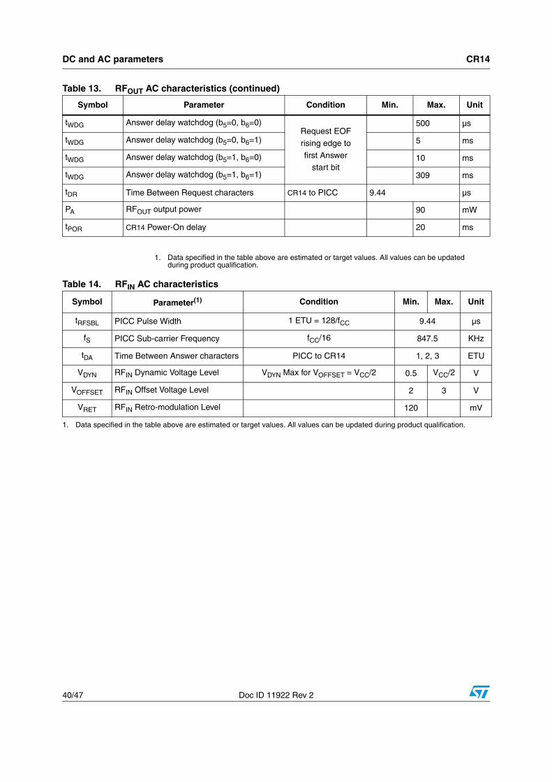
Table 13. RFOUT AC characteristics
Symbol Parameter Condition Min. Max. Unit
fCC External Oscillator Frequency VCC = 5 V 13.553 13.567 MHz
MICARRIER Carrier Modulation Index MI=(A-B)/(A+B) 10 14 %
tRFR, tRFF 10% Rise and Fall time 0.5 1.5 µs
tRFSBL Pulse Width on RFOUT 1 ETU = 128/fCC 9.44 µs
tJIT ASK modulation bit jitter CR14 to PICC -0.5 0.5 µs
t0 Antenna Reversal delay Min = 64/fS 75 µs
t1 Synchronization delay Min = 80/fS 94 µs
DC and AC parameters CR14
40/47 Doc ID 11922 Rev 2
1. Data specified in the table above are estimated or target values. All values can be updated during product qualification.
tWDG Answer delay watchdog (b5=0, b6=0)Request EOF
rising edge to
first Answerstart bit
500 µs
tWDG Answer delay watchdog (b5=0, b6=1) 5 ms
tWDG Answer delay watchdog (b5=1, b6=0) 10 ms
tWDG Answer delay watchdog (b5=1, b6=1) 309 ms
tDR Time Between Request characters CR14 to PICC 9.44 µs
PA RFOUT output power 90 mW
tPOR CR14 Power-On delay 20 ms
Table 13. RFOUT AC characteristics (continued)
Symbol Parameter Condition Min. Max. Unit
Table 14. RFIN AC characteristics
Symbol Parameter(1) Condition Min. Max. Unit
tRFSBL PICC Pulse Width 1 ETU = 128/fCC 9.44 µs
fS PICC Sub-carrier Frequency fCC/16 847.5 KHz
tDA Time Between Answer characters PICC to CR14 1, 2, 3 ETU
VDYN RFIN Dynamic Voltage Level VDYN Max for VOFFSET = VCC/2 0.5 VCC/2 V
VOFFSET RFIN Offset Voltage Level 2 3 V
VRET RFIN Retro-modulation Level 120 mV
1. Data specified in the table above are estimated or target values. All values can be updated during product qualification.

CR14 Package mechanical
Doc ID 11922 Rev 2 41/47
10 Package mechanical
In order to meet environmental requirements, ST offers these devices in different grades of ECOPACK® packages, depending on their level of environmental compliance. ECOPACK® specifications, grade definitions and product status are available at: www.st.com. ECOPACK® is an ST trademark.

Package mechanical CR14
42/47 Doc ID 11922 Rev 2
Figure 36. SO16 narrow - 16 lead plastic small outline, 150 mils body width, Package outline
1. Drawing is not to scale.
Table 15. SO16 narrow - 16 lead plastic small outline, 150 mils body width, package mechanical data
SymbolMillimeters Inches
Typ. Min. Max. Typ. Min. Max.
A 1.75 0.0689
A1 0.1 0.25 0.0039 0.0098
A2 1.25 0.0492
b 0.31 0.51 0.0122 0.0201
c 0.17 0.25 0.0067 0.0098
D 9.9 9.8 10 0.3898 0.3858 0.3937
E 6 5.8 6.2 0.2362 0.2283 0.2441
E1 3.9 3.8 4 0.1535 0.1496 0.1575
e 1.27 0.05
h 0.25 0.5 0.0098 0.0197
L 0.4 1.27 0.0157 0.05
k 0° 8° 0° 8°
Tolerance millimeters inches
ccc 0.1 0.0039
CR14 Ordering information
Doc ID 11922 Rev 2 43/47
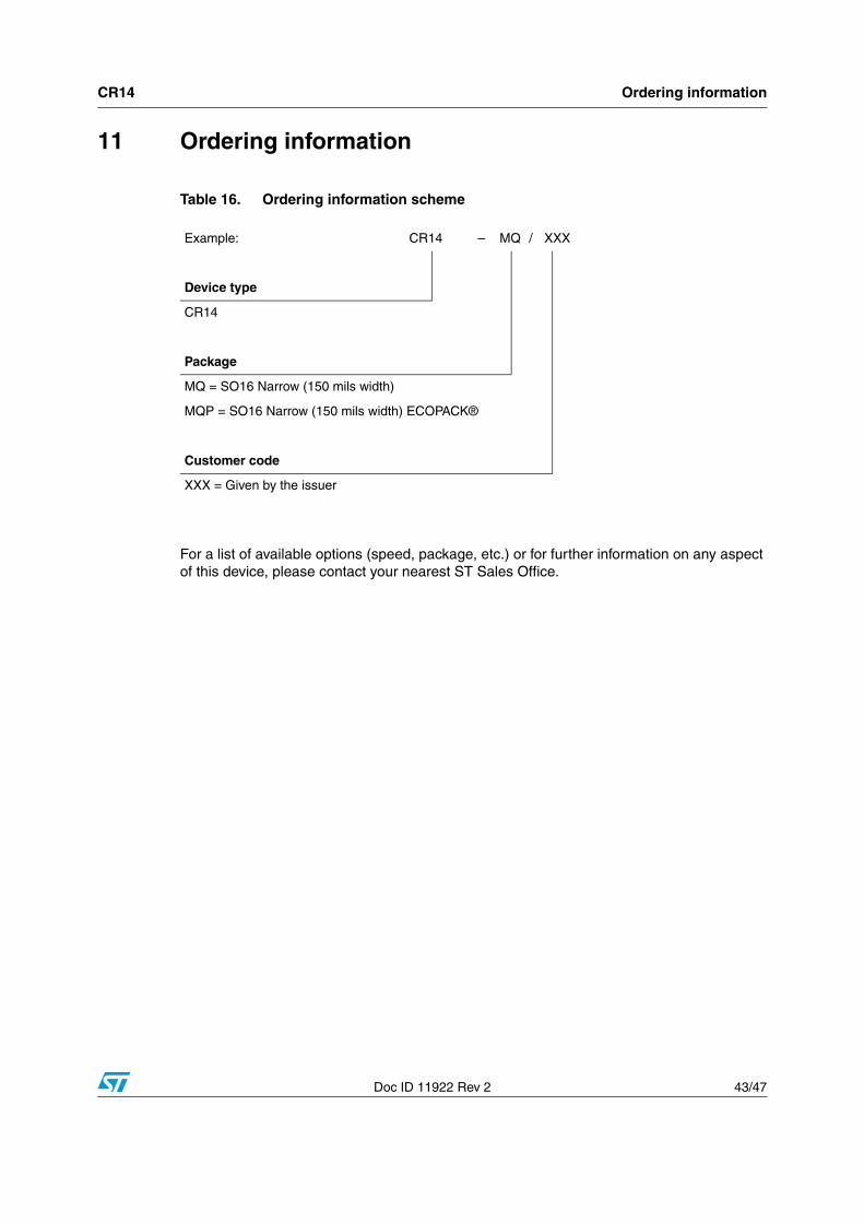
11 Ordering information
For a list of available options (speed, package, etc.) or for further information on any aspect of this device, please contact your nearest ST Sales Office.
Table 16. Ordering information scheme
Example: CR14 – MQ / XXX
Device type
CR14
Package
MQ = SO16 Narrow (150 mils width)
MQP = SO16 Narrow (150 mils width) ECOPACK®
Customer code
XXX = Given by the issuer

ISO14443 type B CRC calculation CR14
44/47 Doc ID 11922 Rev 2
Appendix A ISO14443 type B CRC calculation
#include <stdio.h>
#include <stdlib.h>
#include <string.h>
#include <ctype.h>
#define BYTEunsigned char
#define USHORTunsigned short
unsigned short UpdateCrc(BYTE ch, USHORT *lpwCrc)
{
ch = (ch^(BYTE)((*lpwCrc) & 0x00FF));
ch = (ch^(ch<<4));
*lpwCrc = (*lpwCrc >> 8)^((USHORT)ch << 8)^((USHORT)ch<<3)^((USHORT)ch>>4);
return(*lpwCrc);
}
void ComputeCrc(char *Data, int Length, BYTE *TransmitFirst, BYTE *TransmitSecond)
{
BYTE chBlock; USHORTt wCrc;
wCrc = 0xFFFF; // ISO 3309
do
{
chBlock = *Data++;
UpdateCrc(chBlock, &wCrc);
} while (--Length);
wCrc = ~wCrc; // ISO 3309
*TransmitFirst = (BYTE) (wCrc & 0xFF);
*TransmitSecond = (BYTE) ((wCrc >> 8) & 0xFF);
return;
}
int main(void)
{
BYTE BuffCRC_B[10] = {0x0A, 0x12, 0x34, 0x56}, First, Second, i;
printf("Crc-16 G(x) = x^16 + x^12 + x^5 + 1");
CR14 ISO14443 type B CRC calculation
Doc ID 11922 Rev 2 45/47
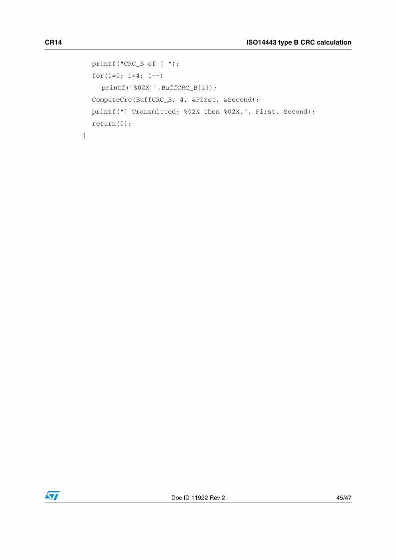
printf("CRC_B of [ ");
for(i=0; i<4; i++)
printf("%02X ",BuffCRC_B[i]);
ComputeCrc(BuffCRC_B, 4, &First, &Second);
printf("] Transmitted: %02X then %02X.", First, Second);
return(0);
}

Revision history CR14
46/47 Doc ID 11922 Rev 2
Revision history
Table 17. Document revision history
Date Revision Changes
16-Dec-2005 1 Initial release.
19-Mar-2010 2 Updated Figure 36 and Table 15 on page 42
CR14
Doc ID 11922 Rev 2 47/47
Please Read Carefully:
Information in this document is provided solely in connection with ST products. STMicroelectronics NV and its subsidiaries (“ST”) reserve theright to make changes, corrections, modifications or improvements, to this document, and the products and services described herein at anytime, without notice.
All ST products are sold pursuant to ST’s terms and conditions of sale.
Purchasers are solely responsible for the choice, selection and use of the ST products and services described herein, and ST assumes noliability whatsoever relating to the choice, selection or use of the ST products and services described herein.
No license, express or implied, by estoppel or otherwise, to any intellectual property rights is granted under this document. If any part of thisdocument refers to any third party products or services it shall not be deemed a license grant by ST for the use of such third party productsor services, or any intellectual property contained therein or considered as a warranty covering the use in any manner whatsoever of suchthird party products or services or any intellectual property contained therein.
UNLESS OTHERWISE SET FORTH IN ST’S TERMS AND CONDITIONS OF SALE ST DISCLAIMS ANY EXPRESS OR IMPLIEDWARRANTY WITH RESPECT TO THE USE AND/OR SALE OF ST PRODUCTS INCLUDING WITHOUT LIMITATION IMPLIEDWARRANTIES OF MERCHANTABILITY, FITNESS FOR A PARTICULAR PURPOSE (AND THEIR EQUIVALENTS UNDER THE LAWSOF ANY JURISDICTION), OR INFRINGEMENT OF ANY PATENT, COPYRIGHT OR OTHER INTELLECTUAL PROPERTY RIGHT.
UNLESS EXPRESSLY APPROVED IN WRITING BY AN AUTHORIZED ST REPRESENTATIVE, ST PRODUCTS ARE NOTRECOMMENDED, AUTHORIZED OR WARRANTED FOR USE IN MILITARY, AIR CRAFT, SPACE, LIFE SAVING, OR LIFE SUSTAININGAPPLICATIONS, NOR IN PRODUCTS OR SYSTEMS WHERE FAILURE OR MALFUNCTION MAY RESULT IN PERSONAL INJURY,DEATH, OR SEVERE PROPERTY OR ENVIRONMENTAL DAMAGE. ST PRODUCTS WHICH ARE NOT SPECIFIED AS "AUTOMOTIVEGRADE" MAY ONLY BE USED IN AUTOMOTIVE APPLICATIONS AT USER’S OWN RISK.
Resale of ST products with provisions different from the statements and/or technical features set forth in this document shall immediately voidany warranty granted by ST for the ST product or service described herein and shall not create or extend in any manner whatsoever, anyliability of ST.
ST and the ST logo are trademarks or registered trademarks of ST in various countries.
Information in this document supersedes and replaces all information previously supplied.
The ST logo is a registered trademark of STMicroelectronics. All other names are the property of their respective owners.
© 2010 STMicroelectronics - All rights reserved
STMicroelectronics group of companies
Australia - Belgium - Brazil - Canada - China - Czech Republic - Finland - France - Germany - Hong Kong - India - Israel - Italy - Japan - Malaysia - Malta - Morocco - Philippines - Singapore - Spain - Sweden - Switzerland - United Kingdom - United States of America
www.st.com