irradiation of diamond-like carbon films by picosecond laser · pdf file ·...
TRANSCRIPT

JLMN-Journal of Laser Micro/Nanoengineering Vol. 10, No. 1, 2015
43
Irradiation of Diamond-like Carbon Films by Picosecond Laser Pulses Liutauras MARCINAUSKAS*1, Alfonsas GRIGONIS*1, Mindaugas GEDVILAS*2, Lina VIGRICAITĖ*1, Gediminas
RAČIUKAITIS*2, Živilė RUTKŪNIENĖ*1, and Marius ČERNAUSKAS*1
*1Kaunas University of Technology, Studentų str. 50, LT-44029 Kaunas, Lithuania E-mail: [email protected]
*2Center for Physical Sciences and Technology, Savanorių Ave. 231, LT-02300 Vilnius, Lithuania
The picosecond laser irradiation of diamond-like carbon (DLC) film on the silicon was investigat-ed. The DLC films were irradiated by Nd:YVO4 laser with the infrared (1064 nm, fluency 1.02 J/cm2) and ultraviolet (355 nm, fluency 0.79 J/cm2) wavelengths with 1, 10, and 100 pulse numbers per spot. The energy dispersive X-ray spectroscopy and microRaman spectroscopy measurements indicated that the full ablation area of the DLC was narrower than laser beam radius of the 1064 nm wave-length with 10 and 100 pulses. The increase of the oxygen concentration was obtained near the abla-tion areas after irradiation with the first harmonic. The microRaman and SEM measurements demon-strated that the DLC film was fully ablated in the laser spot when the third harmonic was used. The formation of silicon carbide (SiC) in the center of the irradiated spot was found after 100 pulses.
Keywords: Picosecond laser irradiation, diamond-like carbon, laser ablation, graphitization
1. Introduction The surface modification of solids by various laser
pulses has been studied for a wide range of materials [1-3]. Nowadays surface modification studies of the thin film semiconductors, especially amorphous carbon films by various types of energetic beams, including laser beam are of great technological and fundamental interest [4-10].
The unique physical, mechanical, optical, and electrical properties of amorphous carbon films, such as diamond-like carbon (DLC) or tetrahedral amorphous carbon (ta-C) are attractive for applications in microelectronincs, sensor technologies, solar photonic, tribological and biomedical fields [10-12]. It was demonstrated that it is possible to create periodical structures or ripple patterns not only on target surfaces of various materials, but even on surfaces with various semiconductors films such as DLC, SiC, GaN, and etc [4, 7-9]. Recent researches showed that DLC peri-odic structures have potential applications in lithography or high density data storage [7].
Lasers induced processes in amorphous carbon films, especially on the surface are influenced by the film materi-al properties (sp2 and sp3 sites fraction, hydrogen concen-tration) and laser parameters (wavelength, pulse duration, number of pulses, repetition rate etc.) [12-19]. Y. Dong et al. [13] reported that the ablation threshold of DLC films decreases with increasing number of pulses. T. Roch et al. [9, 14] demonstrated that the direct laser interference pat-terning of ta-C films reduce the coefficient of friction up to ~30 %. N.T. Panagiotopoulas et al. [6] observed the for-mation of SiC at the a-C:H film/Si interface and film graphitization, when 35 ps laser irradiation with the 1064 nm and 266 nm, respectively, was used. P. Patsalas [12] managed to vary the structural features and optical proper-ties (refractive index) of a-C:H by picosecond laser radia-tion. G.Miyaji et al. [7, 16] demonstrated the nanostructure formation on the DLC surface irradiated at low fluence of femtosecond laser pulses.
The ablation and modification of the DLC films by the nanosecond laser pulses are stipulated by the thermal pro-cesses and are already well widely investigated. Meanwhile the 2D and 3D nanostructuring of the surfaces with pico-second laser pulses is attractive and promising tool. Alt-hough the physical and thermal processes induced in the DLC films by ps laser pulses are not understood yet and well explained. So far no satisfactory researches have been made investigating the picosecond laser pulses effect on the DLC films.
To investigate the influence of the picosecond laser beam wavelength and pulse number on the surface mor-phology and structure of the DLC films were the main pur-pose of the work was.
2. Experimental setup The diamond-like carbon (DLC) film was deposited on
the silicon substrate by radio frequency chemical vapour deposition technique using acetylene gas. The thickness of the DLC film was ~300 nm, the refractive index was 2.03, hardness was ~25 GPa, Young’s modulus - 190 GPa. The DLC film was irradiated with a picosecond Nd:YVO4 laser (Ekspla PL10100) using the first (1064 nm) and the third (355 nm), harmonics. The irradiation was performed using the 1.02 J/cm2 and 0.79 J/cm2 fluency for the first and the third harmonics, respectively. The pulse duration was 10 picoseconds, while the repetition rate was 100 kHz. The radius (r) of the laser beam spots, measured at 1/e2 level were 30 µm and 15 µm for the first and the third harmonics, respectively. The pulse number was 1, 10, and 100 per spot. The films surface morphology was investigated by scan-ning electron microscope (SEM) JEOL JSM6490LV. The irradiated films were analyzed using microRaman spectros-copy (Renishaw inVia spectrometer, 633 nm, 100 s, 1 mW, spot size 2 µm). The energy dispersive X-ray spectroscopy (EDS) (Bruker Quad 5040 spectrometer) was used for the measurement of elemental composition.
DOI: 10.2961/jlmn.2015.01.0009

JLMN-Journal of Laser Micro/Nanoengineering Vol. 10, No. 1, 2015
44
3. Results and discussions The spectrum of the non-irradiated DLC indicates a D
(1274 cm-1) and G (1499 cm-1) peaks (Fig. 1). The full width at half-maxima (FWHM) of the D band (∆D) was 217 cm-1, while FWHM of the G band (∆G) was 174 cm-1. The integral intensity ID/IG ratio was 0.53. Such ID/IG ratio is typical for the DLC films, indicating that the sp3 C-C sites fraction are dominating among the sp2 carbon [11].
1000 1200 1400 1600 18000,0
2,0x10⁴
4,0x10⁴
6,0x10⁴
8,0x10⁴
1,0x10⁵
ID/IG-0.53G-1499 cm-1
DG-174 cm-1
D-1274 cm-1
DD-217 cm-1
Inten
sity,
a.u.
Raman shift, cm-1
The EDS results of the DLC film before and after laser irradiation are given in the Table 1. It should be noted that the EDS was measured in the depth exceeding the film thickness. The d parameter indicates the distance (radius)
from the laser spot center, where EDS measurements were performed.
The irradiation of DLC film by the first harmonic with a single pulse at 1.02 J/cm2 partly removes the film from the Si substrate. The ablated spot diameter is about 30 µm (Fig. 2a). Splats of DLC films still could be found at higher imagination on the surface. The carbon concentration de-creased down to 21.8 at.%, while oxygen increased twice (Table 1). Also such laser fluency influenced to the for-mation of the chaotically distributed ripples (Fig. 2a). The various size micro-fragments outside the ablated area are chaotically distributed. The elemental composition is simi-lar to non-radiated film in radius zone of 15 µm ≤ d ≤30 µm from the center. The melted Si substrate zone (with diameter of ~30 µm) appeared with the increase of the
number of pulses up to 10. The melted silicon area is sur-rounded by the micro-ripple pattern zone (Fig. 2b). The carbon content decreased down to 5.6 at.%, while the oxy-gen concentration increased up to 4.6 at.% in the melted zone.
The hole of 10 µm depth and ~20 µm diameter was ob-served after irradiation with 100 pulses. EDS results indi-cated very low amount of carbon (2.9 at.%) and oxygen (1.1 at.%). However similar to 10 pulses per spot, the nar-row ripple zone around the hole also was formed (Fig. 2c). EDS measurements showed only 18 at.% of carbon and high concentration (30.3 at.%) of oxygen in the radius area 20 µm ≤ d ≤40 µm from the center. It should be noted that even at d>40 µm away from the spot center the oxygen
Table 1 Elemental compositions of the DLC film/substrate before and after laser irradiation by 1064 nm
Puls e number
Dis t ance f rom the spot
cent er , µ m
C, a t .%
O , a t .%
Si , a t .%
DLC - 55 .1 2 .0 42 .9 1 d≤15 21 .8 4 .1 74 .1 1 d≥15 58 .0 4 .3 37 .7
10 d<10 5 .6 4 .6 89 .8 10 15≤d≤30 49 .9 5 .6 44 .5
100 d<10 2 .9 1 .1 96 .0 100 20≤d≤40 18 .0 30 .3 51 .7 100 d>40 41 .7 16 .3 42 .0
Fig. 2 Surface morphology of DLC films irradiated by the first harmonic with 1.02 J/cm2 at different laser pulses
a) 1, b) 10, and c) 100.
(a)
(b)
(c)
Fig. 1 µRaman spectrum of the DLC film.
JLMN-Journal of Laser Micro/Nanoengineering Vol. 10, No. 1, 2015
45
fraction was higher compared to the non-affected DLC film (Table 1).
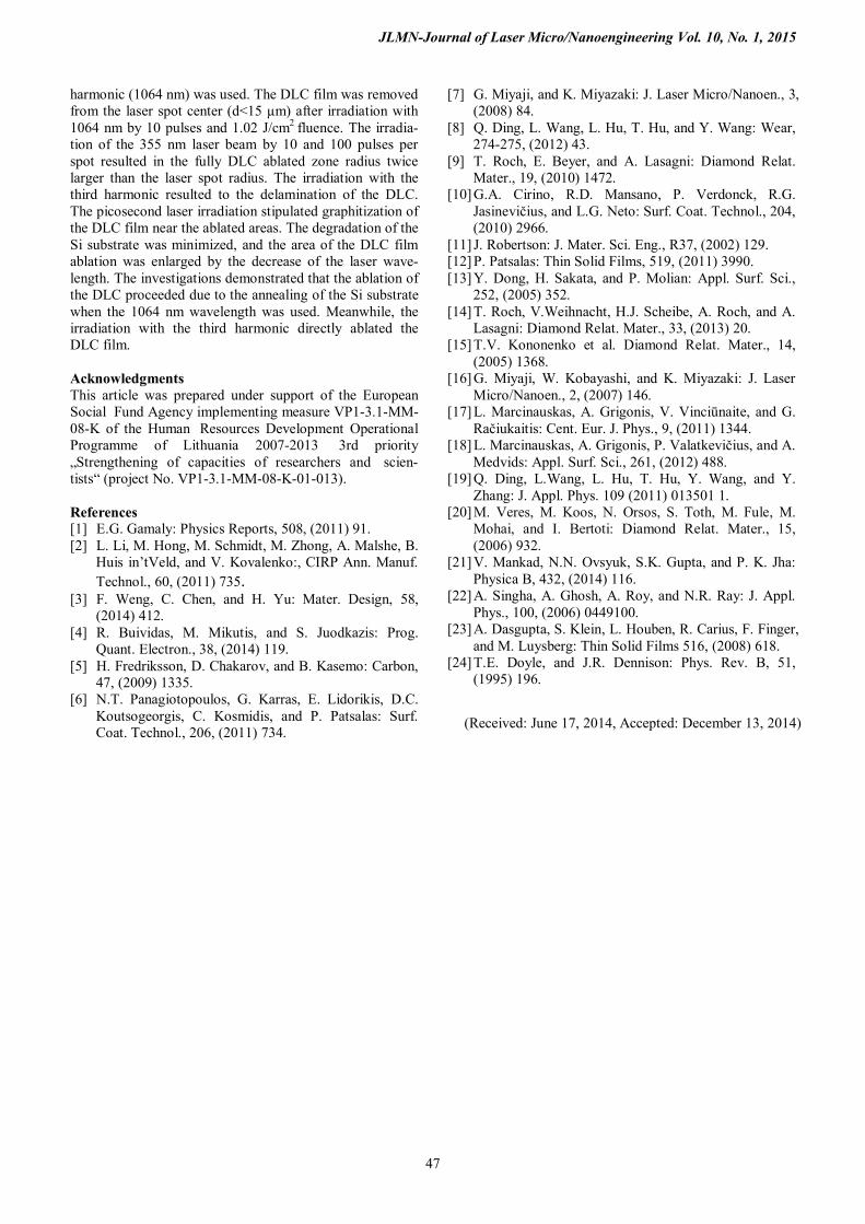
The µRaman spectrum measured from the spot center irradiated by 100 laser pulses indicates the low intensity D (1335 cm-1) and G (1591 cm-1) peaks, and intense broad band at ~960 cm-1 (Fig. 3 b). The broad band can be de-convoluted into several Gaussian peaks. The peak around 960 cm−1 is attributed to the Si (2nd order) and the peak around 980-1020 cm−1 corresponds to the stretching mode of Si–O–Si configuration in which Si atoms were in turn back bonded to the oxygen atoms [20-21]. The EDS and RS measurements confirmed that DLC film was removed in the laser spot center. Existence of low intensity D and G peaks can be conditioned feet back DLC fragments after films spallation. Moreover, it is also probably that the low amount of carbon is dissolved into Si substrate. The D (1338 cm−1) and G (1588 cm−1) peaks became separated in the µRS spectrum measured at the 20 µm ≤ d ≤ 40 µm zone (Fig. 3a). The ∆D peak narrowed to 127 cm−1, while ∆G narrowed to 101 cm−1. As a result of this, ID/IG ratio increased up to 1.27. The increase of the ID/IG ratio repre-sents a reduction of the amount of sp3 C-C sites and an in-crease of the amount of the graphite structure [11]. The appearance of the low intensity peaks at ~1120 cm−1 and ~1480 cm−1 are assigned to trans-polyacetylene segments at grain boundaries [20, 22]. These results indicate that the modified film is composed from a mixture of sp3/ sp2 sites with dominant sp2 C=C sites and formation of the nano-crystalline graphite or glass carbon phase.
800 1000 1200 1400 1600 1800200
700
1200
1700
2200
2700Si-O-Si Si
(b)
ID/IG-2.40
G-1591 cm-1
DG-78 cm-1D-1335 cm-1
DD-116 cm-1
Inten
sity,
a.u.
Raman shift, cm-1
800 1000 1200 1400 1600 180015000
17000
19000
21000
23000
25000Si-O-Si Si
(a)
ID/IG-1.27
G-1588 cm-1
DG-101 cm-1D-1338 cm-1
DD-127 cm-1
Inten
sity,
a.u.
Raman shift, cm-1
The irradiation by the first harmonic demonstrated the
increase of the ablation area with the increase of the pulse numbers. The radius of ablation zone was smaller than the radius of the laser beam spot measured at 1/e2 level. The DLC film fully ablation occurs only in the 15-20 µm radius area depending on the pulse number.
The explanation of obtained results is related with band gap of the irradiated DLC film and Si substrate. The photon
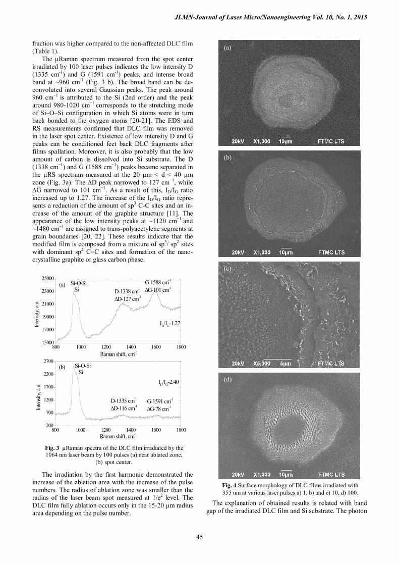
Fig. 4 Surface morphology of DLC films irradiated with 355 nm at various laser pulses a) 1, b) and c) 10, d) 100.
(a)
(b)
(d)
Fig. 3 µRaman spectra of the DLC film irradiated by the 1064 nm laser beam by 100 pulses (a) near ablated zone,
(b) spot center.
(c)

JLMN-Journal of Laser Micro/Nanoengineering Vol. 10, No. 1, 2015
46
energy (1.165 eV) of the laser beam is below the energy band gap of DLC (1.5 – 2 eV) film, for the case of the 1064 nm wavelength, but it is above the band gap of Si (1.11 eV). Thereby the laser photons can pass through DLC film and then be absorbed by silicon substrate inducing local anneal-ing. The increase of the pulse number rises the temperature in the irradiated zone, which induces melting of the Si and formation of pinholes in the substrate as well.
The irradiation of the DLC film with a single pulse at 0.79 J/cm2 induced the uneven ablation and slight stratifi-cation of the film (Fig. 4a). The DLC film was ablated and Si substrate was local melted in the area of ~60 µm diame-ter when irradiation by 10 pulses per spot was used (Fig. 4b). The ablated zone is surrounded by the terrace-like re-lief (Fig. 4c). The appearance of such structure demon-strates the multilayer delamination.
Different morphology depending on the position in the laser spot is observed at the surface after 100 pulses (Fig. 4d). In the radius of the laser spot d≤15 µm, the energy fluence was high to ablate the DLC film and to melt and ablate the silicon substrate. The DLC layer was ablated and the formation of non-regular ripples around the melted Si was observed (15 µm ≤ d ≤ 30 µm). The DLC film was ablated and micro size fragments on the surface were dis-tributed at position 30 µm ≤ d ≤ 40 µm (Fig. 4d). The µRaman spectrum of the melted and ripples formation are-as showed a broad peak (~960 cm-1) indicating amor-phous/nanocrystalline Si and Si-O-Si sites [20]. Also a broad low intensity peak at ~820 cm-1 was observed (Fig. 5). The peak at 820 cm-1 is attributed to the silicon carbide (SiC) [6, 23]. The µRaman spectrum does not demonstrate any D and G peaks, indicating that the film is completely ablated.
800 1000 1200 1400 1600 18000
2000
4000
6000
8000
10000
12000
14000 SiSi-O-Si
SiC
Ripple area
Spot center
Inten
sity,
a.u.
Raman shift, cm-1
The DLC film was modified at the distance higher than d≥ 40 µm. The spectrum of modified carbon film is com-posed from the superposition of separated D (1349 cm-1) and G (1576 cm-1) peaks (Fig. 6). The appearance of the peak at 1473 cm-1 is related to the trans-polyacetylene seg-ments [20]. However, this peak can be related to the A1' mode for five membered rings [24]. The position of D and G bands shifted to higher wave numbers, and both peaks narrowed, compared to non-radiated DLC film (Fig. 6). The ID/IG ratio increased from 0.53 up to 1.31. The rise of
the D band and peaks splitting are the indication of the graphitization of the DLC film [18].
1000 1200 1400 1600 18000
1x10⁴
2x10⁴
3x10⁴
4x10⁴
5x10⁴
1473 cm-1
D-1349 cm-1
DD-161 cm-1G-1576 cm-1
DG-123 cm-1
ID/IG-1.31
Inten
sity,
a.u.
Raman shift, cm-1
The irradiation of the 355 nm laser beam resulted in the
fully DLC ablated zone radius twice larger than the laser spot radius at 1/e2 level. The dimension of the ablated DLC zones increases with the increase of the number of the pulses. The increase of the ablation zone related to the laser beam wavelength. The photon energy of the 355 nm laser beam is ~3.5 eV. Thus the photon energy is higher than the energy band gap of DLC film and Si substrate as well as above the spectral energy of the π−π* interband transition. It will results the strong optical absorption in the volume of the carbon film and laser annealing of the DLC film. The annealing of the a-C:H film by the 266 nm laser beam was obtained by N.T. Panagiotopoulas et al. [6].
The laser photon energy is absorbed by the film, not reaching the silicon substrate when one pulse is used. The delamination of the film after one pulse reflects the spatial distribution of Gaussian beam intensity. The fluency of 0.79 J/cm2 was enough to reach the melting temperature and start the evaporation of the DLC in the center of laser spot. The Gaussian energy distribution of the laser beam resulted non-homogeneous heating and temperature distri-bution in the film. The ablated area is increasing with the number of laser pulses due to accumulation of the energy. The irradiated DLC film is graphitized, the swelled surface is removed and finally the energy is transformed to the Si substrate resulting to the melting and partly ablation (Fig. 4d). G. Miyaji et al. [16] obtained changes in the bonding structure from DLC to graphite carbon certainly proceeds the ablation to form the nanostructures. T. Roch [14] found that at low fluences (<500 mJ/cm2) the ablation rate is low and the surface swelling (graphitization) is dominating compared to the film ablation. However in our case, the fluence of 0.79 J/cm2 was high enough to induce the graph-itization of the film and when partly ablate the film even after one pulse.
4. Conclusions
The radius of ablated zone was smaller than the radius of the laser beam spot measured at 1/e2 level when the first
Fig. 5 µRaman spectra of the DLC film irradiated with the 355 nm laser beam by 100 pulses.
Fig. 6 µRaman spectrum of the DLC film after irradiation with the 355 nm laser beam by 100 pulses at d > 40 µm
distance.
JLMN-Journal of Laser Micro/Nanoengineering Vol. 10, No. 1, 2015
47
harmonic (1064 nm) was used. The DLC film was removed from the laser spot center (d<15 µm) after irradiation with 1064 nm by 10 pulses and 1.02 J/cm2 fluence. The irradia-tion of the 355 nm laser beam by 10 and 100 pulses per spot resulted in the fully DLC ablated zone radius twice larger than the laser spot radius. The irradiation with the third harmonic resulted to the delamination of the DLC. The picosecond laser irradiation stipulated graphitization of the DLC film near the ablated areas. The degradation of the Si substrate was minimized, and the area of the DLC film ablation was enlarged by the decrease of the laser wave-length. The investigations demonstrated that the ablation of the DLC proceeded due to the annealing of the Si substrate when the 1064 nm wavelength was used. Meanwhile, the irradiation with the third harmonic directly ablated the DLC film.
Acknowledgments This article was prepared under support of the European Social Fund Agency implementing measure VP1-3.1-MM-08-K of the Human Resources Development Operational Programme of Lithuania 2007-2013 3rd priority „Strengthening of capacities of researchers and scien-tists“ (project No. VP1-3.1-MM-08-K-01-013). References [1] E.G. Gamaly: Physics Reports, 508, (2011) 91. [2] L. Li, M. Hong, M. Schmidt, M. Zhong, A. Malshe, B.
Huis in’tVeld, and V. Kovalenko:, CIRP Ann. Manuf. Technol., 60, (2011) 735.
[3] F. Weng, C. Chen, and H. Yu: Mater. Design, 58, (2014) 412.
[4] R. Buividas, M. Mikutis, and S. Juodkazis: Prog. Quant. Electron., 38, (2014) 119.
[5] H. Fredriksson, D. Chakarov, and B. Kasemo: Carbon, 47, (2009) 1335.
[6] N.T. Panagiotopoulos, G. Karras, E. Lidorikis, D.C. Koutsogeorgis, C. Kosmidis, and P. Patsalas: Surf. Coat. Technol., 206, (2011) 734.
[7] G. Miyaji, and K. Miyazaki: J. Laser Micro/Nanoen., 3, (2008) 84.
[8] Q. Ding, L. Wang, L. Hu, T. Hu, and Y. Wang: Wear, 274-275, (2012) 43.
[9] T. Roch, E. Beyer, and A. Lasagni: Diamond Relat. Mater., 19, (2010) 1472.
[10] G.A. Cirino, R.D. Mansano, P. Verdonck, R.G. Jasinevičius, and L.G. Neto: Surf. Coat. Technol., 204, (2010) 2966.
[11] J. Robertson: J. Mater. Sci. Eng., R37, (2002) 129. [12] P. Patsalas: Thin Solid Films, 519, (2011) 3990. [13] Y. Dong, H. Sakata, and P. Molian: Appl. Surf. Sci.,
252, (2005) 352. [14] T. Roch, V.Weihnacht, H.J. Scheibe, A. Roch, and A.
Lasagni: Diamond Relat. Mater., 33, (2013) 20. [15] T.V. Kononenko et al. Diamond Relat. Mater., 14,
(2005) 1368. [16] G. Miyaji, W. Kobayashi, and K. Miyazaki: J. Laser
Micro/Nanoen., 2, (2007) 146. [17] L. Marcinauskas, A. Grigonis, V. Vinciūnaite, and G.
Račiukaitis: Cent. Eur. J. Phys., 9, (2011) 1344. [18] L. Marcinauskas, A. Grigonis, P. Valatkevičius, and A.
Medvids: Appl. Surf. Sci., 261, (2012) 488. [19] Q. Ding, L.Wang, L. Hu, T. Hu, Y. Wang, and Y.
Zhang: J. Appl. Phys. 109 (2011) 013501 1. [20] M. Veres, M. Koos, N. Orsos, S. Toth, M. Fule, M.
Mohai, and I. Bertoti: Diamond Relat. Mater., 15, (2006) 932.
[21] V. Mankad, N.N. Ovsyuk, S.K. Gupta, and P. K. Jha: Physica B, 432, (2014) 116.
[22] A. Singha, A. Ghosh, A. Roy, and N.R. Ray: J. Appl. Phys., 100, (2006) 0449100.
[23] A. Dasgupta, S. Klein, L. Houben, R. Carius, F. Finger, and M. Luysberg: Thin Solid Films 516, (2008) 618.
[24] T.E. Doyle, and J.R. Dennison: Phys. Rev. B, 51, (1995) 196.
(Received: June 17, 2014, Accepted: December 13, 2014)