investigations on synthesis, purification and characterization of indium antimonide
TRANSCRIPT

International Journal of Innovative Research in Advanced Engineering (IJIRAE) ISSN: 2349-2763 Issue 02, Volume 4 (February 2017) www.ijirae.com ]]
____________________________________________________________________________________________________ IJIRAE: Impact Factor Value – SJIF: Innospace, Morocco (2015): 3.361 | PIF: 2.469 | Jour Info: 4.085 |
Index Copernicus 2014 = 6.57 © 2014- 17, IJIRAE- All Rights Reserved Page -36
Investigations on Synthesis, Purification and Characterization
of Indium Antimonide
Chidanandappa. J1, Eswara Prasad. K2, Mani V. N3. NRSC, Hyderabad JNT University, Hyderabad C-MET, Hyderabad Abstract: The Indium antimonide (InSb) is one of the promising optoelectronic materials having potential applications in the development of data storage, frequency, parametric oscillations, detectors and related gadgets. Purity of material plays a vital role in the development of quality devices for space and defence related high-end applications. Directional Solidification System (DSS) plays a major role in reducing the vibrations during the synthesis and crystallization process to yield high and pure InSb compound. This paper discusses homogenization, synthesis, purification and characterization of Indium antimonide. Directional Solidification System (DSS) is employed for the preparation of pure InSb crystalline material. This system is fabricated with a view to establish required and suitable temperature isotherms at top and bottom of the furnace and also to tackle the irregularities of sample during the process of cooling the aspects. The crystallization of homogenized pure sample is kept under vacuum in the furnace. The impurities of the InSb are segregated at the bottom end of the sample. The purity analysis of the InSb sample is studied and presented by employing XRD, TEM, SEM, EDS, ICP-OES, Raman and FTIR techniques.
Key words: Optoelectronic materials, Detectors, Indium Antimonide (InSb), Homogenization, Directional Solidification, Temperature isotherms, Characterization, Purity analysis
1. INTRODUCTION
The Indium antimonide is one of the III-IV Ternary and Quaternary Lattice materials, used for making high speed electronic devices. Consequently, Indium antimonide based devices are now emerged in Research and Development activities. High pure InSb compound could be used in the fabrication of various optoelectronic devices which include LEDs, transistors, lasers, photovoltaic cells and infrared detectors, etc.[1-3]. Devices made from InSb work in the band gap range of 0.17eV, wavelength 6.2µm at 300K .There are certain other characteristics associated with InSb which include high mobility, low electron mass and matching of lattice with select III-IV Ternary and Quaternary materials. These properties make the InSb the most suitable substrate material. The major advantages of InSb are largest electron magnetic moment, effective electron mass (0.014mo) , electron mobility 7.7 X 10⁻⁴cm2/Vs , low dislocations density , low concentration and low cost. The synthesis, homogenization, purification and crystallization experiments of Indium antimonide compound are carried out by using vertical directional freezing, and solidification systems.
Indium antimonide is first homogenized and then purified by melting and solidification processes. This homogenized and purified InSb is subjected to directional freezing/crystallization for 20 pass cycles. To prevent the contamination of InSb with other gaseous impurities, the top end of the crucible is sealed with vacuum. The crucible is made to travel at the rate of 2.5 cm hr-1 after placing it in the directional solidification system. The starting material of Indium and Antimony are used as input materials to produce crystals and epitaxial structures. It is difficult to produce high purity Indium antimonide compound consistently due to intricacies involved the in analysis of impurities at low ppb levels. Metallic impurities such asBi,Pb, Mg, , Fe, As, Te, C and O are present in Indium antimonide. The purity of 99.999 (5N) is referred as nano-pure electronic grade. For 5N+ pure metal, the total amount of select impurities must be less than 100ppb for metallic and 600ppb for other alloys. Methods proposed by Bridgman and Czchralski are widely employed to grow the bulk InSb crystals.[4-5] However, literature studies revealed certain structural defects in the grown bulk crystals employed by the Bridgman technique .Gaseous impurities like carbon and oxygen are minimized within a range of 1 to 10 ppb range.

International Journal of Innovative Research in Advanced Engineering (IJIRAE) ISSN: 2349-2763 Issue 02, Volume 4 (February 2017) www.ijirae.com ]]
____________________________________________________________________________________________________ IJIRAE: Impact Factor Value – SJIF: Innospace, Morocco (2015): 3.361 | PIF: 2.469 | Jour Info: 4.085 |
Index Copernicus 2014 = 6.57 © 2014- 17, IJIRAE- All Rights Reserved Page -37
If these impurities are not thoroughly reduced during the synthesis, then the compounds show deep and shallow energy levels within the energy band gap leading to failure of the device performance [6-7]. The high pure materials have wide variety of applications and the global requirements are continuously increasing. Hence, improving the quality of compound has become a necessity and useful to undertake this task under controlled conditions. The stringent analysis of the compound characterization for its purity is very much needed. Such analysis could be employed by using the mass spectrometry like Inductively Coupled Plasma Mass Spectrometry (ICP-MS) and Glow Discharge Mass Spectrometry (GDMS). Subsequently purity analysis could also be performed by using the residual resistivity ratio analysing techniques.
2. DESIGN AND DEVELOPMENT OF PROCESSING SYSTEM
The inherent issues encountered during the process of ultra high purification of InSb are the design and development of test-rig , process modelling, capability demonstration , maintaining of narrow solid-liquid regions using several heaters and coolers embedded in a single control panel, the movement of sample tube with respect to its rate and direction, heat transfer, reduction of temperature loss etc. Majority of the literature reported research works on the growth and characterization of InSb are employed by using the vertical gradient freezing technique for controlled and vibration less growth of quality crystals. Directional Solidification System (DSS) is primarily built for synthesis and purification of InSb compounds comprises several sub-systems like furnace, control system, translation assembly and a rotational assembly. The experimental setup of DSS employed is depicted in Fig.1.
Certain considerations are taken into account during the design of DSS furnace which includes distribution of temperature at different locations within the furnace; temperature at the top of the furnace should be high as compared to the bottom of the furnace.DSS is thermally regulated to make sure that the melting point of the furnace should always be equal to midpoint of the sharp temperature drop. At the bottom, the temperature drop might be more rapid compared to the top of the furnace. However, it is to be ensured that this rapid drop should not go beyond the threshold, resulting in irregularities in cooling the sample. Temperature at the bottom is maintained nearly at room temperature. The furnace is comprised of the kanthal based heating elements which are wounded around a quality ceramic tube of 2mm wall thickness. Indium antimonide is synthesized from high pure elements chosen in 50:50 ratio using, an electric furnace.
The mixing furnace which produces the two molten zones along the ampoule tube is powered by1000W to attain a temperature of 10000C. Other parameters of the tube include 10mm diameter with a length of 150mm. The tube is covered with ceramic powder coating material insulation to sustain at temperature up to 1000oC. The furnace is designed for two zones to attain a maximum of 10000C and continuous operating temperature is 9000C. The highest and the lowest temperature zone length is 100mm and having a gradient zone length of 450mm.
Fig.1 Schematic diagram of directional solidification system (DSS)
The Platinum Rhodium thermo couple is located near to the heating element and connecting the middle of the high temperature zone for measurement of temperature. High quality heat retardant quartz wool and ceramic bricks are used for fabrication of furnace. During continuous operation of the furnace, a stainless enclosure protects the furnace to maintain reasonably low temperature.

International Journal of Innovative Research in Advanced Engineering (IJIRAE) ISSN: 2349-2763 Issue 02, Volume 4 (February 2017) www.ijirae.com ]]
____________________________________________________________________________________________________ IJIRAE: Impact Factor Value – SJIF: Innospace, Morocco (2015): 3.361 | PIF: 2.469 | Jour Info: 4.085 |
Index Copernicus 2014 = 6.57 © 2014- 17, IJIRAE- All Rights Reserved Page -38
he system is vibration free up and provides translational and rotational movement to the ampoule with specified speed. The Sample tube movement and rotation are provided by the mechanical driven system program to rotate at 20-40 RPM The PLC based controlling system which is a subsystem of the DSS which is meant to control the temperature of furnace. Apart from PLC, the DSS is also associated with thyristor based controllers for controlling the power voltages, a temperature transmitter to regulate the output signal, a programmable logic controller for conversion between analogy and digital and vice-versa. The stepper motor starts running with a driver unit to position the ampoule at desired location [8-12].Lab view software package takes the job of controlling the DSS interfaced through PLC. Data logging software computer interface facility is utilized for processing the furnace parameters, storage of data and its analysis.
2.1 SEGREGATION OF IMPURITIES
The segregation is characterized by the distribution coefficient, K of a metal in solvent. The equilibrium distribution coefficient K0 can be defined by the isothermal ratio of normal concentrations on the curves of solidus, Cs to liquids, C1.The distribution coefficient Ko =Cs/C1. The impurities with K0>1, accumulate at the beginning of the ingot and K0<1 at the tail end of the refined and purified ingot. The knowledge of distribution coefficients is important for prediction of refining efficiency.There are various factors which are influencing the refining process include: (a) Zone travel rate (b) Direction of zone movement (c) Zone size and length of sample (d) Temperature gradient (e) Diameter of the sample tube (f) Thermal conductivities of phases (g) Latent heat of fusion h) Density difference between the solid and liquid (i) Speed of crystal formation (j) Surface tension of the liquid (k) Tendency of the liquid to cool.
3. EXPERIMENTAL DETAILS
Experimentation is aimed to segregate certain impurities likeAg, Al, Cu, Fe, Sn, Zn, Ge, Pb and Cdduring the purification and crystallization processes of InSb. During the process of homogenization, treated In and Sb starting materials are loaded into the pre-cleaned and treated quartz ampoule and sealed vacuum of 5 x 10⁻⁶Torr level shown in (Fig.2). The tube is subjected to periodic rotation both in clockwise and anticlockwise for facilitating through mixing of the molten elements to form InSb compound. Indium (In) and antimony (Sb) are taken in 1:1 ratio for the preparation of homogenized sample. The Indium is etched with HNO3 and antimony with acquaregia to reduce their oxide layer present on the surface.
Fig.2: Indium and antimony loaded vacuum sealed- sample tube Fig.3: Crystallized Indium antimony ingot
The sample is melted at 5500C and the molten charge is rapidly cooled at 100 C and again re-melted with 12 hrs pass(es) and 20 cycle (s) scheme. The obtained sample is taken out from the ampoule in the clean room (1000 class/100 class bench) environment and crushed into powder. The finely crushed powder sample is once again loaded into the pre-treated, cleaned quartz ampoule and is sealed with vacuum of 10-6Torr level.[13] Then loaded ampoule with sample is subjected to vertical directional freezing and solidification (530-5500C). The process is carried with 12 hrs pass time, travel rate of 2.5-3.5 cm.hr-1, rate of rotation at 30-40 rpm and 10 cycles-pass (es) scheme. The ampoule is cooled to ambient temperature.Crystallized charge-ingot is shown in Fig.3. The prepared purified sample is studied for their purity and other properties employing XRD, SEM, TEM, EDS, ICP-OES FT-IR and Raman Spectra methods. Requiredsafety precautions are followed while handling InSb. Major cleaning procedure includes treatment of starting materials, washing with acetone, methanol and nano-pure water, cleaning of crucible with super pure aqua regia to remove oxide layer etc are followed at different stages ofcrucible and sample cleaning.

International Journal of Innovative Research in Advanced Engineering (IJIRAE) ISSN: 2349-2763 Issue 02, Volume 4 (February 2017) www.ijirae.com ]]
____________________________________________________________________________________________________ IJIRAE: Impact Factor Value – SJIF: Innospace, Morocco (2015): 3.361 | PIF: 2.469 | Jour Info: 4.085 |
Index Copernicus 2014 = 6.57 © 2014- 17, IJIRAE- All Rights Reserved Page -39
4. RESULTS AND DISCUSSIONS Fig.4 shows XRD patterns of the InSb sample is recorded in the range of 2 theta between 4˚ and 80˚ using CuK radiation. The XRD results show that the purified InSb is of highly ordered and Poly-Crystalline type and dominant orientations such as (111), (220), (311), (422) and (511) are observed. The calculated lattice spacing d=3.7266 A0,2 (degree) =23.8783. This data is also compared with the ASTM, JCPDS 7-215 standards. The relative peak intensity is proportional to the crystalline material perfection, the higher the peak, the higher the quality of crystal. The large counts, sharp peaks reveal the reduction in defects level. Fig.5 shows SEM-EDAX results that the prepared InSb sample contain contaminants including oxygen, carbon and other impurities. It also reveals the presence and formation of discrete micro regions of impurities, inclusions, segregates, and micro cracks is present in the sample (Fig.6a-d). Different surface morphology, microstructure features are observed and grains become densely packed as seen in SEM micro-graphs. The grain size varies and the average grain size is 1 µm, 2 µm, 10 µm and 200 µm. These microstructures are invariably observed at the centre of the ingot and the length gradually decreases towards the direction of periphery.
Fig. 4 XRD Spectrum of InSb
Fig.5. SEM-EDAX –InSb
Fig-6b.SEMImage ofInSb,original mag = 75 K x2 µm scalebar=6.6 mm
Fig-6a. SEM Image of InSb, original mag = 75 K x 1 µm scale bar=6.6 mm

International Journal of Innovative Research in Advanced Engineering (IJIRAE) ISSN: 2349-2763 Issue 02, Volume 4 (February 2017) www.ijirae.com ]]
____________________________________________________________________________________________________ IJIRAE: Impact Factor Value – SJIF: Innospace, Morocco (2015): 3.361 | PIF: 2.469 | Jour Info: 4.085 |
Index Copernicus 2014 = 6.57 © 2014- 17, IJIRAE- All Rights Reserved Page -40
Fig. 7(a-d) shows TEM images having significant high resolution of 500Nm under bright field. The contrast of images is due to absorption of electrons in the material composition and thickness of material. The dislocations originate from the interface and propagate with InSb sample. At two nano meter the higher magnificent transparency structure and texture are significant. Moire pattern is seen in the micrograph with spacing and bending characteristics. Misfit fringes could be due to variation in orientation of crystal planes. The grid high lights the crystalline faces and dark areas show the lattice spacing of crystallites. It is also observed that the dislocations and crystal defects inside the bulk sample. The high density of material shows the improved quality of material.
Inductively Coupled Plasma Optical Emission Spectrometry (ICP-OES) is employed to estimate the specific targeted impurities such as Ag, Al, Cu, Fe, Sn, Ga, Zn, Ge, Pb and Cd. Purity analysis results of starting In, Sb and purified Indium antimonide samples are presented in table 1 and 2 respectively. The results show that there is a significant improvement in purity (5N+) in which the total impurity concentration is reduced in the purified InSb sample. Presence of some of the impurities might be due to the experimental contamination or accidental redistribution of these impurities instead of segregation. The qualitative trend of impurity (ies) segregation on to the different locations of the rod (ends) is observed.
Table1. Purity test results of purified In and Sb by ICP-OES (ppm) ICP-OES – Detection limit 0.10ppm
Table2. Purity test results of purified InSb by ICP-OES (ppm) ICP-OES – Detection limit 0.10ppm
Element In Sb Element InSb Ag Al Cu Fe Sn Ga Zn Ge Pb Cd Si
1.00 12.60 7.10 5.60 9.58 2.70 6.50 1.80 14.20 3.14 2.78
2.25 14.30 4.50 2.67 7.20 1.80 4.40 3.20 24.30 2.92 5.00
Ag Al Cu Fe Sn Ga Zn Ge Pb Cd Si
0.50 1.20 0.80 1.40 1.22 1.20 1.30 0.30 3.43 1.20 1.10
Fig-6c. SEM Image of InSb, original mag = 75 K x 10 µm scale bar=6.6 mm
Fig-6d. SEM Image of InSb, original mag = 75 K x 200 µm scale bar=6.6 mm
Fig.-7a Fig.-7d Fig.-7c Fig.-7b
International Journal of Innovative Research in Advanced Engineering (IJIRAE) ISSN: 2349-2763 Issue 02, Volume 4 (February 2017) www.ijirae.com ]]
____________________________________________________________________________________________________ IJIRAE: Impact Factor Value – SJIF: Innospace, Morocco (2015): 3.361 | PIF: 2.469 | Jour Info: 4.085 |
Index Copernicus 2014 = 6.57 © 2014- 17, IJIRAE- All Rights Reserved Page -41
Table1. Purity test results of purified In and Sb by ICP-OES (ppm) ICP-OES – Detection limit 0.10ppm
Table2. Purity test results of purified InSb by ICP-OES (ppm) ICP-OES – Detection limit 0.10ppm
Element In Sb Element InSb Ag Al Cu Fe Sn Ga Zn Ge Pb Cd Si
1.00 12.60 7.10 5.60 9.58 2.70 6.50 1.80 14.20 3.14 2.78
2.25 14.30 4.50 2.67 7.20 1.80 4.40 3.20
24.30 2.92 5.00
Ag Al Cu Fe Sn Ga Zn Ge Pb Cd Si
0.50 1.20 0.80 1.40 1.22 1.20 1.30 0.30 3.43 1.20 1.10
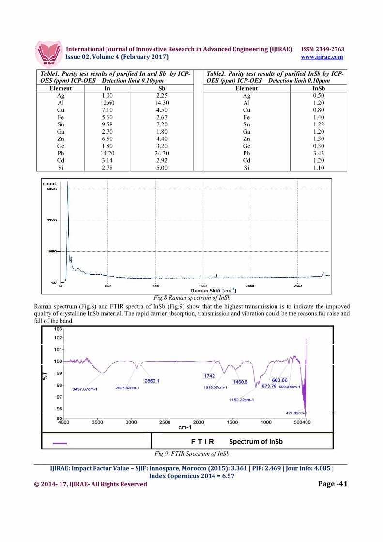
Fig.8 Raman spectrum of InSb
Raman spectrum (Fig.8) and FTIR spectra of InSb (Fig.9) show that the highest transmission is to indicate the improved quality of crystalline InSb material. The rapid carrier absorption, transmission and vibration could be the reasons for raise and fall of the band.
Fig.9. FTIR Spectrum of InSb
Spectrum of InSb

International Journal of Innovative Research in Advanced Engineering (IJIRAE) ISSN: 2349-2763 Issue 02, Volume 4 (February 2017) www.ijirae.com ]]
____________________________________________________________________________________________________ IJIRAE: Impact Factor Value – SJIF: Innospace, Morocco (2015): 3.361 | PIF: 2.469 | Jour Info: 4.085 |
Index Copernicus 2014 = 6.57 © 2014- 17, IJIRAE- All Rights Reserved Page -42
5. CONCLUSION
Directional solidification system (DSS) is designed and developed for the preparation of 5N+ pure InSb compound. The performance and the capability of the developed system are demonstrated through the preparation, synthesis, and purification of the InSb compound. The potential application of high pure compound material is exploiting in the numerous devices globally. The process parameters such as Temperature Gradient, creation and maintaining of narrow solid-liquid regions, crucible type, vacuum level, sample tube rotational speed and movement of direction are studied and optimized. Prepared InSb sample is thus characterized by employing XRD, SEM, TEM, EDX, ICP-OES, Raman and FT-IR studies. The results indicate the improvement in purity and structural properties.
REFERENCES [1]. P.S Dutta and H.L. Bhatt- “The physics and technology of gallium antimonide: An optoelectronic material J. Appl Phys
1997:81(9):5821–5870. [2]. N. K. Udayashankar and H.L. Bhat Bull Mater. “Growth and characterization of Indium antimonide and gallium
antimony crystals “Bulletin of Material. Science Vol.24 No.5, 2001, pp445-453 [3]. V.N. Mani. K Ghosh K and Balaraju., “Preparation of pure crystalline Indium and its characterization” Material
Science Research, vol 5(1), (2008) pp83-88. [4]. Dattatray B. Gadkari, “Advances of the Vertical Directional Solidification Technique for the Growth of High Quality
InSb Bulk Crystals” J. Chem. Chem Eng. Vol.6 (2012) pp250-258. [5]. Dattatray B. Gadkari, “Advances of the Vertical Directional Solidification Technique for the Growth of High Quality
InSb Bulk Crystals” J. Chem. Chem Eng. Vol.6 (2012) pp250-258. [6]. K. Ghosh , V.N. Mani, ST Ali, M.R.P. Reddy, K Balaraju, S. Dhar “Study on the segregation characterization of
impurities in Gallium and its ulta purification by multi pass zone refining”- Metals Materials and processes , 2008, Vol 20,2, PP.153-160
[7]. K. Ghosh K, V.N. Mani and S. Dhar, “A modeling approach for purification of group III metal ( Ga and In) by zone refining. J.Appl. Phy, 104,1 2008, 311, 1521-1528, (2009)
[8]. E. Papis–Polakowska “ surface treatment of GaSb nad related materials for the processing of MiD –infrared semiconductor devices” Electron Technology International journal 37/38(2005/2006),4, pp.1-34
[9]. R. Ramesh babu, G. Bhagavannarayana and K Rama Murthy “Studies on bulk growth and micro structural characterization of 4-aminobenzophenone single crystal growth from vertical Bridgeman technique” Bull.Mater.Sci . Vol.xx No.x Month 2013 pp1-6
[10]. S.P Prabahkaran, R. Ramesh Babu, and K Ramamurthi” design of fabrication of eight zone vertical dynamic gradient freeze system for organic single crystal growth” Review of Scientific instruments 84,083907(2013)
[11]. S.P. Prabahkaran, R. Ramesh Babu, M. Sukumaran, G. Bhagavannarayana, and K Rama Murthy “Investigation on the growth and characterization of 4-aminobenzophenone single crystal by vertical dynamic gradient freeze technique. Journal of Crystal Growth 390 (2014) pp18-23
[12]. K. Ghosh K , V.N. Mani and S. Dhar, “Numerical study and experimental investigation of zone refining in ultra-high purification of gallium and its use in the growth of GaAs epitaxial layers” Journal of Crystal Growth 311(6):1521-1528 · March 2009
[13]. D.B Gadkari, “Detached Growth: Unfolding Four Decades Growth Mystery into Vertical Directional Solidification Technique on Earth” International Journal of Scientific and Research Publications, Vol.4, Issue 5, May 2014, ISSN 2250-3153, pp1-10.