investigation and design of low - chalmers publication...
TRANSCRIPT

Improving landfill monitoring programswith the aid of geoelectrical - imaging techniquesand geographical information systems Master’s Thesis in the Master Degree Programme, Civil Engineering
KEVIN HINE
Department of Civil and Environmental Engineering Division of GeoEngineering Engineering Geology Research GroupCHALMERS UNIVERSITY OF TECHNOLOGYGöteborg, Sweden 2005Master’s Thesis 2005:22
Investigation and Design of LowPhase Noise and WidebandMicrowave VCOsMaster’s Thesis in Wireless and Photonics Engineering
MINHU ZHENG
Department of Microtechnology and NanoscienceCHALMERS UNIVERSITY OF TECHNOLOGY
Goteborg, Sweden 2012

Investigation and Design of Low Phase Noise and Wideband Microwave VCOs
© MINHU ZHENG, 2012
Master’s Thesis 2012
Department of Microtechnology and NanoscienceChalmers University of TechnologySE-41296 GoteborgSweden
Tel. +46-(0)31 772 1000
Reproservice / Department of Microtechnology and NanoscienceGoteborg, Sweden 2012

Investigation and Design of Low Phase Noise and Wideband Microwave VCOsMaster’s Thesis in the Master’s programme in Wireless and Photonics Engineering
MINHU ZHENGDepartment of Microtechnology and NanoscienceChalmers University of Technology
Abstract
This thesis studied the design techniques of low phase noise and wideband microwavevoltage controlled oscillators (VCOs) used for point-to-point radio applications. First,basic oscillator theories as well as different technologies were reviewed. Then two C-band MMIC VCOs were designed in a commercial InGaP HBT foundry process withdifferent topologies, namely the balanced Colpitts and the balanced Clapp. The circuitswere simulated with a commercial harmonic balance simulator and the designs wereoptimized for the best phase noise performance by studying the implication of variousdesign parameters, such as tank quality factors, transistor current density, feedbackcapacitor ratio and etc. Simulation results show over 10% tuning range for both topolo-gies and a phase noise of -122 dBc/Hz at 100 kHz offset for the balanced Clapp, 10 dBsuperior to that of the balanced Colpitts, owing to a higher current excitation.
Keywords: Voltage Controlled Oscillator, Microwave Monolithic Integrated Circuit,Heterojunction Bipolar Transistor, Phase Noise
iii CHALMERS, Master’s Thesis 2012:Minhu Zheng

CHALMERS, Master’s Thesis 2012:Minhu Zheng iv

Contents
Abstract iii
Contents iv
Acknowledgements vii
1. Introduction 1
2. Oscillator Background 3
2.1. Basics of Oscillating System . . . . . . . . . . . . . . . . . . . . . . . . . . 32.2. Resonator Technology . . . . . . . . . . . . . . . . . . . . . . . . . . . . . 42.3. Active Device Technology . . . . . . . . . . . . . . . . . . . . . . . . . . . 5
2.3.1. Two-terminal diodes . . . . . . . . . . . . . . . . . . . . . . . . . . 52.3.2. Three-terminal transistors . . . . . . . . . . . . . . . . . . . . . . . 5
2.4. Oscillator Topologies . . . . . . . . . . . . . . . . . . . . . . . . . . . . . . 72.5. Voltage Controlled Oscillators (VCOs) . . . . . . . . . . . . . . . . . . . . 92.6. Small Signal Loop Gain Analysis . . . . . . . . . . . . . . . . . . . . . . . 112.7. Large Signal Analysis . . . . . . . . . . . . . . . . . . . . . . . . . . . . . . 142.8. Phase Noise Basics . . . . . . . . . . . . . . . . . . . . . . . . . . . . . . . 15
2.8.1. Noise sources . . . . . . . . . . . . . . . . . . . . . . . . . . . . . . 152.8.2. Transistor noise modeling . . . . . . . . . . . . . . . . . . . . . . . 162.8.3. Phase noise modeling . . . . . . . . . . . . . . . . . . . . . . . . . 17
2.9. CAD Simulation . . . . . . . . . . . . . . . . . . . . . . . . . . . . . . . . . 19
3. MMIC VCO Design 21
3.1. Design Specifications . . . . . . . . . . . . . . . . . . . . . . . . . . . . . . 213.2. Design Strategies . . . . . . . . . . . . . . . . . . . . . . . . . . . . . . . . 213.3. Design Parameters Optimization . . . . . . . . . . . . . . . . . . . . . . . 27
3.3.1. Tank quality factor . . . . . . . . . . . . . . . . . . . . . . . . . . . 273.3.2. Bias Current Density . . . . . . . . . . . . . . . . . . . . . . . . . . 283.3.3. Transistor Arrangement . . . . . . . . . . . . . . . . . . . . . . . . 293.3.4. Feedback Capacitor Ratio and Value . . . . . . . . . . . . . . . . . 303.3.5. Varactor Bias Choke . . . . . . . . . . . . . . . . . . . . . . . . . . 32
v CHALMERS, Master’s Thesis 2012:Minhu Zheng

3.4. Simulation Results . . . . . . . . . . . . . . . . . . . . . . . . . . . . . . . 333.4.1. Balanced Colpitts VCO . . . . . . . . . . . . . . . . . . . . . . . . . 333.4.2. Balanced Clapp VCO . . . . . . . . . . . . . . . . . . . . . . . . . . 333.4.3. Summary and Discussion . . . . . . . . . . . . . . . . . . . . . . . 34
4. Conclusion 39
5. Future Work 41
References 43
A. Equivalent Tank Impedance 47
CHALMERS, Master’s Thesis 2012:Minhu Zheng vi

Acknowledgements
I owe my deepest gratitude to my supervisors from Ericsson AB, Joakim Een andDr.Biddut Banik for granting me the opportunity to participate in this industrial thesisas well as their patient guidance and persistent support throughout this work. Withouttheir effort, it would have been impossible to finish the thesis.
I am indebted to my academic supervisor from Chalmers University of Technology,Dr.Dan Kuylenstierna for his supervision during the literature study phase and valu-able ideas in the later stages. His professional expertise gave me enormous inspirationsand kept me always on the track.
In addition, I would like to thank my teammate, Naiyuan Zhang from Linkping Uni-versity, for the unforgettable memories of being cooperating with each other.
vii CHALMERS, Master’s Thesis 2012:Minhu Zheng

CHALMERS, Master’s Thesis 2012:Minhu Zheng viii

1. Introduction
Microwave technology has evolved enormously during the 20th century.It has beenpenetrating into many aspects of our society, e.g., microwave heating, wireless com-munication systems, military radars and instrumentation. Among the building blocksof a microwave system, the microwave source, or the frequency generation unit, is avital one, since it provides a stable reference signal for the rest of the system.
Microwave sources used to be bulky and expensive in the early era of the microwaveindustry, examples are vacuum tubes in the 1940s and reflex klystrons in the 1970s[1].Late 1970s witnessed more compact versions of microwave oscillator, e.g., Gunn diodeand Si transistor hybrid oscillators. Today, thanks to the advancement in semiconductortechnology, voltage controlled oscillators (VCOs) are available in the form of monolithicmicrowave integrated circuit (MMIC), and their sizes and costs have been reduced con-siderably while still offer excellent performance.
However, the evolution of microwave technology continuously demands higher qual-ity microwave oscillators at lower cost. Taking the microwave backhaul network asan example[2], with the migration to the fourth generation (4G) mobile networks, thepoint-to-point microwave systems connecting the base stations and the core networkare facing enormous challenges in terms of bandwidth efficiency. To this end, modu-lation scheme up to 1024QAM has been implemented[3]. However, as the modulationorder increases, the effects of phase noise will be profound and the oscillator becomesthe bottleneck that limits the performance of the system. The high order modulation,in turn, will pose stringent requirements to the oscillators. Meanwhile, the oscillatorsare always desired to be miniaturized to reduce the costs and possibly to be integratedwith other parts of the transceiver.
The specifications of a VCO include oscillation frequency, phase noise, output power,tuning range, harmonic suppression and etc. Phase noise is defined as the ratio betweenthe noise power at a certain offset frequency from the carrier and the carrier power.It is a critical parameter of a VCO for multi-channel communication systems wherechannels are densely allocated within a limited frequency band. The output power of aVCO should be large enough to drive the following circuits in the transceiver chain, e.g.the mixer. A buffer amplifier is usually utilized in the output stage of the VCO to boostthe signal. VCOs are designed to be able to be tuned over a certain frequency band.Broadband VCOs can offer up to an octave tuning bandwidth. In many applications,both low phase noise and wide tuning range are desired. However, trade-offs must be
1 CHALMERS, Master’s Thesis 2012:Minhu Zheng

made between the two parameters. For a typical C-band VCO, used for the point-to-point radio link, over 10% tuning range is expected while the phase noise should be aslow as -120 dBc/Hz for the entire frequency band.
This Thesis aims to study design techniques of low phase noise wideband MMICVCOs intended for microwave point-to-point radio link applications and understandphase noise mechanism and how to make accurate phase noise prediction. Main objec-tives include literature review on microwave oscillator technologies and topologies, de-sign MMIC VCOs with a commercial foundry process and optimize for the best phasenoise performance.
The study will not cover certain technologies such as MEMS. Agilent ADS and acommercial InGaP HBT process are chosen by default when designing the VCOs sincethey have long been the solution within the company and foundry service is readilyaccessible as well.
The rest of the thesis is organized as follows. Chapter 2 presents oscillator back-ground including technology, topology, phase noise mechanism, computer simulation,and etc. In Chapter 3, two MMIC VCOs are simulated and optimized for phase noiseperformance. Chapter 4 summarizes the findings. Finally, Chapter 5 offers some rec-ommendations for the future work.
CHALMERS, Master’s Thesis 2012:Minhu Zheng 2

2. Oscillator Background
2.1. Basics of Oscillating System
A microwave oscillator can be viewed as a feedback circuit, which consists of an ac-tive device and a resonator, as shown in Figure 2.1. The active device is essentially anamplifier which amplifies the incoming signal, with its output feed to the input of theresonator, which is further connected to the input of the amplifier and forms a feedbackloop. To start oscillation, the loop gain should be larger than unity as well as the loopphase shift should be 0 or a multiple of 360. The loop gain requirement specifies thatthe amplifier should at least provide a gain to compensate the loss of the resonator,while the loop phase condition guarantee the feedback signal to add constructively tothe original signal [4].
A(j)vivo
vf
(j)
Figure 2.1. Oscillator as a feedback system
Another view of microwave oscillators is the so-called negative resistance concept.The active device generates a negative input resistance which compensates the lossesfrom the resonator tank.
Both the active device and the resonator can be implemented with various types ofcomponents. Typical active devices are two terminal diodes, Gunn diode or IMPATTdiode, and three terminal transistors, either a bipolar junction transistor (BJT) or a fieldeffect transistor (FET). The resonator is normally realized by a LC network, a dielectricresonator, or an yttrium iron garnet (YIG).
3 CHALMERS, Master’s Thesis 2012:Minhu Zheng

2.2. Resonator Technology
Metallic cavity resonators have historically been the choice for filter and low phasenoise oscillator applications, due to their extremely high Q factor. Typical phase noiseperformance of metallic cavity oscillators can be as low as -180 dBc/Hz at 10 kHz offsetfor a 10 GHz carrier [5]. However, their bulky size limits them from the most perfor-mance critical applications.
Dielectric resonators are based on low loss, temperature stable, high permittivity andhigh Q ceramic materials with normally a cylindrical shape. They resonate in variousmodes while the dominate TE01δ mode is utilized for temperature stability and Q factoroptimization reasons. Owing to the high permittivity of dielectric materials, their sizecan be made much smaller than that of a metallic cavity resonator resonating at thesame frequency. Moreover, their miniaturized size allows them to be implementedin a planar hybrid MIC technology. Dielectric resonator oscillators (DROs) are usuallyhoused in a metal enclosure to minimize radiation losses; thereby preventing unwantedQ degradation. The oscillation frequency of a DRO can be tuned either electrically ormechanically. A varactor tuned DRO shows a typical tuning range up to 1% whilewith a tuning screw the oscillation frequency can be tuned up 5%. An issue of DROsis their sensitivity to microphonic. Unwanted vibrations can cause more than 20 dBdeterioration in phase noise [6]. A commercially available DRO [7] shows a phase noiseof -122 dBc/Hz at 10 kHz offset and a tuning range from 8 to 8.3 GHz.
Surface acoustic wave (SAW) resonators enable the design of low noise and tempera-ture stable oscillators up to 2 GHz. Their structure consists of an interdigital transducer(IDT) and two reflectors fabricated on a piezoelectric material. The IDT converts acous-tic wave to electrical signal. SAW oscillators have been extensively used as very lownoise sources in wired applications such as optical communications, Gigabit Ethernetcommunications, and storage circuits. A 500 MHz SAW resonator with low noise am-plifier, showing -140 dBc/Hz phase noise at 10 kHz [8], was used to build an 8 GHzSAW oscillator using frequency multiplication technique.
Bulk acoustic wave (BAW) resonators, also known as film bulk acoustic resonators(FBAR), are a recent introduction to build fixed frequency oscillators. They are nor-mally used in the frequency range between 500 MHz and 5 GHz. Typical phase noiseperformance of FBAR oscillator is -112dBc/Hz at 10 kHz at 2 GHz carrier [9]. Majorfoundries are still working hard to bring the FBAR process into mass production.
The most straightforward way to build a resonator is to combine an inductor and acapacitor, i.e. a LC resonator, either in series or in parallel. LC resonators have long beenthe choice for low frequency oscillators and as the evolution of RFIC/MMIC technologythey not long restrict themselves at the low end of the spectrum. Spiral inductors andMIM capacitors are supported by essentially every foundry process while at microwavefrequencies transmission lines are sometimes employed to represent high Q inductors.
CHALMERS, Master’s Thesis 2012:Minhu Zheng 4

VCOs can be built by introducing varactor diodes to the LC resonators. It is possible todesign fully integrated VCOs with LC resonators. The phase noise of an X-band MMICLC VCO can be as low as -110 dBc/Hz at 100 kHz offset and the tuning range can bemore than 10% [10].
YIG-tuned oscillators (YTO) are widely used in test instruments and military systemsrequiring octave tuning bandwidth. By using an YTO, low phase noise and wide tun-ing range can be satisfied simultaneously. The core of the resonator is an yttrium irongarnet (Y3Fe5O3) spherical placed between two poles of a cylindrically re-entrant elec-tromagnet. The resonant frequency is controlled by the applied magnetic field strength.YTOs offer a very high Q, around 4000 at 10 GHz. The YTO can operate at frequencyup to 50 GHz. Typical YTO shows a tuning range of 3 to 11 GHz and phase noise of-128 dBc/Hz at 100 kHz[11].
2.3. Active Device Technology
The active device generates negative resistance in an oscillator and can be either a two-terminal diode or a three-terminal transistor [1].
2.3.1. Two-terminal diodes
The Gunn diode is named after J. B. Gunn who discovered the Gunn Effect in 1962.It is also known as Transferred Electron Device (TED). Only semiconductor materialswith a satellite valley in the conduction band can be made into Gunn diode, such asGaAs and InP. Negative resistance is observed in a region when the electrons transferfrom conduction band to the low mobility satellite valley. Despite their relatively lowefficiency, normally in the order of 2 to 3 percent, Gunn oscillators can deliver low noiseand high power at frequencies up to 100 GHz.
IMPact Ionization Avalanche Transit Time (IMPATT) diodes can offer even greaterpower than Gunn oscillators with a frequency capability beyond 100 GHz. Moreover,they are more efficient, with a typical efficiency from 10 to 20 percent. However, theyshow a roughly 10 dB worse performance in terms of phase noise compared to theirGunn counterparts.
2.3.2. Three-terminal transistors
Three-terminal transistors emerged in the RF and microwave generation field in thelate 1970s and since then they had been replacing diodes in many applications due totheir low cost and high integrability.
Semiconductor transistors can be classified into two categories, i.e, field effect tran-sistors (FETs) and bipolar transistors. The former group comprises mainly metal-oxide-
5 CHALMERS, Master’s Thesis 2012:Minhu Zheng

semiconductor field effect transistors (MOSFETs), metal semiconductor field effect tran-sistors (MESFETs), and High electron mobility transistors (HEMTs) of different mate-rials; while the latter includes Si bipolar junction transistors (BJTs) and heterojunctionbipolar junction transistors (HBTs) of different materials.
CMOS technology has long found its applications in digital and analog integratedcircuits owing to the low cost silicon process and dense integration. With the contin-uous scaling of MOSFETs, the RF performance of the Si MOSFETs has been improvedconsiderably and research shows that the state-of-the-art Si RF MOSFETs can have fT
and fmax exceeding 300 GHz [12] . In the consumer electronics market today, essentiallyall products operating in the lower GHz frequencies are based on CMOS technology.With mixed-signal design techniques, RF function is integrated with digital processingand power management units, occupying only a small corner of the entire chip.
As far as VCO applications are concerned, although their notorious high flicker noisecorner frequency and low breakdown voltage constrain their appearance in the phasenoise critical applications, RF MOSFET can still offer moderate performance given care-ful design and optimization.
GaAs and InP HEMTs can offer excellent performances in applications such as lownoise amplifiers, power amplifiers, and switches up to several hundred GHz. They are,however, seemingly not the best candidate for phase noise critical oscillator applica-tions due to their inherently high 1/f corner frequencies. In spite of this, their superiorhigh frequency performances make it possible to design fundamental oscillators be-yond 100 GHz. In addition, GaN HEMT based oscillators can deliver much higheroutput power, eliminating the need for buffer amplifiers.
Si BJTs are the devices of choice for low phase noise VCO applications at lower GHzfrequencies , owing to their low 1/f noise characteristic. They are mainly available inthe form of discrete devices and therefore used to design hybrid VCOs together withvarious resonator technologies.
HBTs differ from conventional BJTs in the use of hetero structure in the base-emitteror/and the base/collector junctions. They maintain the merit of low flicker noise cornerfrequency as their predecessors while exhibit a much higher fT and fmax, which makesthem attractive devices for microwave oscillator applications.
There are, essentially, two categories of HBTs: Si based HBTs and III-V compoundHBTs. The former one comprises mainly SiGe/Si HBTs and the latter one can be classi-fied into GaAs and InP HBT depending on the base materials being employed. Thesetechnologies can be found in various applications depending on their specific proper-ties, e.g. SiGe HBTs are the best candidate for W-band automotive radar applicationsdue to their high frequency capability and for C-band to X-band MMIC VCO applica-tions, where phase noise is the most critical parameter, InGaP/GaAs based HBTs aredominating due to their high breakdown voltages and superior reliability.
CHALMERS, Master’s Thesis 2012:Minhu Zheng 6

2.4. Oscillator Topologies
Oscillators can have various topologies. Depending on the operation frequency, anoscillator can be built by lumped elements or distribute elements.
At the low end of the microwave frequency range, oscillators are usually imple-mented by lumped components and based on feedback theory. Common topologiesinclude Colpitts, Hartley, Clapp, and cross-coupled. Taking BJT based oscillators as ex-amples, the schematics of Colpitts, Hartley, and Clapp oscillator are shown in Figure2.2 [13]. These topologies share the same properties that the elements connected be-tween the emitter-base and emitter-collector terminals have the same signs in terms ofreactance while that between the base-collector terminals is the opposite. The choicebetween the Colpitts and Hartley oscillators is determined by the operating frequency.For relatively low frequency applications, the Colpitts topology is preferred since in-ductors tend to be large and present low quality factor, so their number should be min-imized. However when it comes to high frequency applications, the Q limiting elementturns to the capacitor as the inductor Q increases with frequency; therefore Hartley so-lution seems more efficient. The Clapp topology resembles the Colpitts except that ituses a series LC network at the base-collector terminals and the extra tapping capacitorcan further increase the tank swing while keeping the transistor below breakdown. TheColpitts oscillator and its variants are favored for low phase noise applications since thenoise current is injected at peaks of the output signal, where the circuit is least sensitiveto noise perturbations [14].
C1
C2 L L1
L2
C
C3
C2
C1 L
a) Colpitts b) Hartley c) Clapp
Figure 2.2. The Colpitts oscillator and its variants
The cross coupled topology consists of two transistors providing 360 phase shift forthe oscillation condition. It is also known as negative-gm oscillator since the impedancelooking into the cross-coupled pair is −2/gm, which compensates for the loss of thetank. The schematic of a cross coupled oscillator is shown in Figure 2.3 [15]. This
7 CHALMERS, Master’s Thesis 2012:Minhu Zheng

topology benefits for relaxed start-up condition and is ubiquitously used in the designof CMOS RFICs.
-2/gm
2LP
CP/2
2RP
Figure 2.3. The cross-coupled oscillator
When the frequency continues to increase, the negative resistance method is pre-ferred when designing oscillators. For this method, the transistor is viewed as a two-port network and the S-parameter data is obtained. By using a proper terminatingnetwork, the transistor enters unstable regions for the desired frequencies, showing anegative resistance at the input. A load network is designed to cancel the reactive partof the input impedance, insuring the circuit oscillates at the desired frequency. A typi-cal negative resistance oscillator with BJT is illustrated in Figure 2.4. As can be seen, itutilized a common base configuration with an inductive feedback at the base terminal.This inductor is used to boost |Γin| and |Γout| [13].
The topologies discussed above are mostly single-ended solutions, and only funda-mental output frequency is available. In practical, a balanced configuration is oftenused in MMIC oscillator design. A push-push structure consists of two symmetric os-cillators and can provide output frequency twice of that of the single oscillator, whichextend the usable frequency range for a given transistor technology. Another advan-tage of the push-push configuration is that it can reduce the phase noise by 3 dB.
The theory of push-push operation is illustrated in Figure 2.5 [16]. As can be seen,the two unit oscillators can operate in both odd mode and even mode. However, for
CHALMERS, Master’s Thesis 2012:Minhu Zheng 8

L
Load
network
Terminating
network
Figure 2.4. The common-base negative resistance configuration
the push-push operation, only the odd mode is desired, which means that the two suboscillators are oscillating out of phase and a virtual ground is formed in the symmetryplane. The oscillation condition can be written as [16],
Re (Zin) + RV < 0 (2.1)
Re (Zin) + RV + 2RL > 0 (2.2)
2.5. Voltage Controlled Oscillators (VCOs)
In most applications, the oscillators are desired to be tuned electronically over a certainfrequency range. The conceptual diagram and the tuning characteristic are shown inFigure 2.6 [15]. The slope of the frequency tuning curve is called the tuning sensitivityand is given by,
KVCO = dωout/dVcont (2.3)
To design a VCO, either the inductor or the capacitor in the tank of the fixed fre-quency oscillator can be replaced by a tunable element. Tunable inductors, however,are implemented using active devices and exhibit excess noise. Therefore, most VCOsutilize tunable capacitors, or varactors, in the tank.
A varactor can be either a p-n junction varactor or a MOS varactor, depending on thetechnology. For a p-n junction varactor, the diode is operating at reverse bias conditionand the junction depletion capacitance is controlled by the tuning voltage. A varactorequivalent circuit is shown in Figure 2.7 [16].
Where CV is the variable capacitor, RS is the series resistor, and LS is the series para-sitic inductor [16].
Three main parameters of a varactor are most concerned by VCO designers. Theyare the reverse breakdown voltage, the capacitance ratio, and the quality factor.
9 CHALMERS, Master’s Thesis 2012:Minhu Zheng

C
RL
LCV
C
LCV
C
L CV
Virtual
ground
C
2RL
L
b) Odd mode equivalent circuit
c) Even mode equivalent circuit
a) A simplified push-push oscillator
Zin
Zin
ZLo
ZLe
Figure 2.5. The push-push topology
The reverse breakdown voltage defines the maximum applied tuning voltage and isdetermined by the technology used and the doping concentration of the junctions.
The capacitance at a given bias voltage is given by [16],
CV (VV) = CV0
(1 +
VV
ϕ
)−γ
(2.4)
Where CV0 is the zero bias junction capacitance, ϕ is the contact potential (1.3V forGaAs) , and γ is the varactor junction sensitivity which is related to the doping profile.For different γ values, a varactor can be classified as abrupt (γ = 0.5) and hyperabrupt(1 < γ < 2). The doping concentrations for an abrupt junction and a hyperabruptjunction are plotted in Figure 2.8 [16]. As can be seen, the abrupt varactor has a uniformdoping profile in the active region while in the hyperabrupt varactor the active regionis nonlinearly doped.
CHALMERS, Master’s Thesis 2012:Minhu Zheng 10

Voltage-Controlled
OscillatorωoutVcont
ωout
Vcont
ω1
V1 V2
ω2
KVCO
ω0
Figure 2.6. VCO characteristic
CV
LSRS
Figure 2.7. Varactor equivalent circuit
The capacitance ratio between the minimum and maximum tuning voltages limitsthe maximum tuning range of a VCO. It can be shown this ratio is also related to γ, anda hyperabrupt varactor can provide a wider tuning bandwidth.
The quality factor of a varactor is given by [16] ,
Q(VV) =1
2π f RSCV(VV)(2.5)
The quality factor is inverse proportional to the frequency and is also a function ofbias voltage. Most venders provide the quality factor data at 50 MHz for historicalreasons, and one can readily extrapolate it to another frequency.
A typical plot of quality factors for the abrupt and hyperabrupt varactors is shown inFigure 2.9 [16]. As can be seen, the hyperabrupt varactor presents a higher QV at highreverse voltages and a lower QV at low reverse voltages. This is due to the fact that athigh voltages, the capacitance of a hyperabrupt varactor decreases more rapidly thanthat of an abrupt varactor.
The quality factor of the varactor is the most critical parameter for low phase noiseVCOs. It is normally much lower comparing with other elements in the resonator cir-cuit and therefore limits the overall tank quality factor.
2.6. Small Signal Loop Gain Analysis
Oscillator small signal loop gain condition can be derived from either the feedback orthe negative resistance point of view, and both methods should give the same result.
11 CHALMERS, Master’s Thesis 2012:Minhu Zheng

Doping density, cm-3
1019
1017
1015
Distance, µm0 1 2 3
Doping density, cm-3
1019
1017
1015
Distance, µm0 1 2 3
a) b)
p+
n
n+p+
n
n+
Figure 2.8. Doping profile of a) abrupt junction and b) hyperabrupt junction
QV
Vt [V]0 5 10 15
0
2000
4000
hyperabrupt
varactor
abrupt
varactor
f=50 MHz
Figure 2.9. Quality factor versus bias voltage for abrupt and hyperabrupt varactors
Here the start-up condition of a single-ended Clapp oscillator is analyzed, using thenegative resistance concept. Similar result can be obtained for a Colpitts oscillator.
The circuit of a single-ended Clapp oscillator and its equivanlent circuit are shownin Figure 2.10. We consider the tank to be the series combinition of L and C3, with thefeedback capacitors C1 and C2 being included in the active device.
The input impedance looking into the active device can be derived as follows,
Vin = Vbe + Ve (2.6)
Vbe =Iin
jωC1(2.7)
Ve =Iin + gmVbe
jωC2=
Iin + gmIin
jωC1
jωC2(2.8)
Zin =Vin
Iin= − gm
ω2C1C2− j(
1ωC1
+1
ωC2
)(2.9)
Where Vbe is the base-emitter voltage and Ve is the emitter voltage.
CHALMERS, Master’s Thesis 2012:Minhu Zheng 12

C1
C2
L
C3
Re
Vcc
C1
C2
L
C3
Re
b
c
e
b
e
a) b)
Zin
+
Vin
-
Iin
gmvbe
Figure 2.10. The schematics of a) single-ended Clapp oscillator and b) its equivalentcircuit
The impedance of the series LC tank is given by,
Zt = Rs + j(
ωL− 1ωC3
)(2.10)
where Rs accounts for the loss in the tank.
Oscillation will start when the following two conditions are met:
Rs < | −gm
ω2C1C2| (2.11)
−(
1ωC1ωC2
)+
(ωL− 1
ωC3
)= 0 (2.12)
Thus the oscillation frequency can be given by,
ωosc =1√
LCtot(2.13)
Where Ctot = 1/(1/C1 + 1/C2 + 1/C3).
A Clapp VCO can be constructed by replacing C3 with a varactor CV . Normally CV ischosen to be much smaller than C1 and C2. the C f can be replaced by a tuned varactorCV . The tuning range can be express as,
13 CHALMERS, Master’s Thesis 2012:Minhu Zheng

TR = 2 ·ωosc,high −ωosc,low
ωosc,high + ωosc,low= 2 ·
1√LCV(1)
− 1√LCV(0)
1√LCV(1)
+1√
LCV(0)
= 2 ·√
CV(0)/CV(1)− 1√CV(0)/CV(1) + 1
(2.14)which is largely dependent on CV .
2.7. Large Signal Analysis
The previous small signal analysis can only guarantee the oscillation to start. As theoscillation amplitude increases, the negative resistance generated by the active devicewill decrease. The negative resistance will ultimately equal to the tank loss, and thecircuit enters steady state. As in the steady state the transistor is usually operatingin non-linear regions, traditional linear analysis techniques could not predict the sig-nal amplitude as well as the oscillation frequency and CAD software with harmonicbalance simulators need to be employed. An analytical method based on describingfunction to calculate the final signal amplitude is presented in [4], and is described herebriefly.
Vi(t)=V1cosωt
VBEQ
VCC
ZL
ic
Figure 2.11. Large-signal analysis of a BJT
Consider a BJT under large-signal conditions, as is shown in Figure 2.11 [4], the base-emitter voltage can be represented by a sinusoid signal added on the DC bias voltage,
vBE = VBEQ + V1 cos ωt (2.15)
And the collector current can be expressed as,
iC = ISevBE/VT = ISeVBEQ/VT ex cos ωt = ICQex cos ωt (2.16)
CHALMERS, Master’s Thesis 2012:Minhu Zheng 14
Where VT = kT/q is the thermal voltage, IS is the saturation current, x(= V1/VT)
represents the signal amplitude.For large-signals, ex cos ωt can be expanded in Fourier series,
ex cos ωt = I0(x) + 2∞
∑n=1
In(x) cos nωt (2.17)
Where In(x)(n = 0, 1, . . . , ) are the modified Bessel functions of the first kind. There-fore the fundamental component of iC is given by 2ICQ I1(x) cos ωt. The large-signaltransconductance Gm(x) is defined as the ratio between the fundamental component ofiC and the voltage V1, and is given as,
Gm(x) =2ICQ I1(x)
V1=
2IC,dc I1(x)VTxI0(x)
= gm2I1(x)xI0(x)
(2.18)
where gm is the small-signal transconductance.For large drive level, Gm(x) ≈ 2gm, so the fundamental frequency component of the
collector current can be approximated by twice the collector DC current.
2.8. Phase Noise Basics
2.8.1. Noise sources
The noise sources in an oscillator system can be classified into three main types: thermalnoise, shot noise and flicker noise. They are caused by different mechanisms and aredescribed as follows.
Thermal noise is caused by the random thermal motion of the charge carriers, andcan be always found in any conductor or semiconductor device at temperature aboveabsolute zero [16]. It is also known as white noise since its value is independent offrequency. The thermal noise associated with a resistor can be represented by a seriesvoltage source or a parallel current source. In the case of current source, the meansquare value of noise current can be written as,
⟨i2n⟩= 4kT∆ f /R (2.19)
Where k is the Boltzmann constant and equals 1.38× 10⁻²³ J/K, T is the temperaturein Kelvin, and ∆ f is the bandwidth in Hz.
Shot noise is originated from the discrete nature of charge carriers that constitute thecurrent flow. In a forward biased p-n junction, the potential barrier can be overcome bythe carriers with higher thermal energy. The mean square shot noise current is givenby,
15 CHALMERS, Master’s Thesis 2012:Minhu Zheng

⟨i2n⟩= 2qI∆ f (2.20)
where q is the electron charge.Flicker noise, also called 1/f noise, is a low frequency noise with power spectral
density proportional to f−γ, with γ being close to unity. The mechanism and origin offlicker noise are complicated and it is generally believed that the flicker noise is causedby surface effect of semiconductor materials. The mean square flicker noise current canbe expressed as,
⟨i2n⟩= KF× IAF ∆ f
f−γ(2.21)
where KF is the flicker noise coefficient, AF is the flicker noise exponent, and I is theDC current. Both KF and AF are device dependent and can be extracted by measure-ment.
2.8.2. Transistor noise modeling
The challenge in accurate phase noise prediction, especially close-in phase noise, lies intwo major aspects: the modeling of the noise sources in the active device, as well as theway in which harmonic balance simulator treats the cyclostationary noise sources.
rb rcCc
gmVπ
i2
nb rπ
i2nc
i2nere
Cπ
+
Vπ
-
be2
nb e2nc
c
e
Figure 2.12. HBT model with noise sources
The HBT equivalent circuit with noise sources is shown in Figure 2.12. As can beseen, it consists of three voltage sources representing the thermal noise associated withresistances of the terminals, two current sources representing shot noise from the base-emitter and collector-base junctions respectively. Flicker noise is represented by a cur-rent source across the base-emitter junction and is combined with the base shot noise.The mean square values of the voltage and current sources can be given as follows [16],
CHALMERS, Master’s Thesis 2012:Minhu Zheng 16

⟨e2
nb⟩= 4kTRb∆ f (2.22)⟨
e2nc⟩= 4kTRc∆ f (2.23)⟨
e2ne⟩= 4kTRe∆ f (2.24)⟨
i2nb⟩= 2qIb∆ f + KF× IAF
b∆ ff
(2.25)⟨i2nc⟩= 2qIc∆ f (2.26)
2.8.3. Phase noise modeling
Ideally, the spectrum of an oscillator output shows only one component at the carrierfrequency. However, in the real world, phase noise and harmonics can also be observed.The phase noise of an oscillator is a measure of the signal purity and is defined as theratio between the noise power at offset frequency ∆ω and the carrier power. The phasenoise is often characterized in 1 Hz bandwidth and expressed in decibel, in other words,it has a unit of dBc/Hz.
There are numerous models analytically expressing the phase noise of an oscillator,among which the Leeson′s model and the Lee and Hajimiri′s model are most used.The former model is based on linear time invariant (LTI) assumption while the latterassumes a linear time variant (LTV) system.
The renowned Leeson′s formula was initially introduced by D.B Leeson in 1966 andcan be written as [17],
L (∆ω) = 10 · log2FkTPs·[
1 +(
ω0
2QL∆ω
)2]·(
1 +∆ωc
|∆ω|
) (2.27)
where F is the device effective noise factor, Ps is the oscillation signal power, ω0 is theoscillation frequency, QL is the tank loaded Q, ∆ω is the offset frequency from carrierwhere phase noise is measured, ∆ωc is the corner frequency between the 1/ f 2 and 1/ f 3
slope region. The typical phase noise spectrum based on Leeson′s formula can be seenin Figure 2.13.
Leeson′s equation is empirical and thus has certain limitations, for example the fac-tor F is a fitting parameter and has no analytical expression. In spite of that, it givesinsights into design techniques to minimize the phase noise in most oscillator applica-tions. These include:
1. Maximize the quality factor of the resonator tank.
2. Maximize the voltage swing in the resonator tank but avoid reaching the satura-tion region and the breakdown voltage.
17 CHALMERS, Master’s Thesis 2012:Minhu Zheng

L(fm)
-30 dB/
decade
-20 dB/
decade
fc f0/2QL f
Figure 2.13. Phase noise spectrum from Leeson′s equation
3. Choose a transistor with the lowest possible flicker noise corner frequency.
The more recent Lee and Hajimiri′s model introduced the concept of impulse sensi-tivity function (ISF) which encodes information about the sensitivity of the oscillator toan impulse injected at a certain phase. The maximum value of the ISF appears near thezero crossing of the oscillation. The ISF is denoted by Γ (ω0τ) and can be expressed as,
Γ (ω0τ) =c0
2+
∞
∑n=1
cn cos (nω0τ) (2.28)
The phase noise in the 20 dB slope region is given by,
L (∆ω) = 10 log
i2n
∆ fΓ2
rms
2q2max∆ω2
(2.29)
While in the 30 dB slope region, it can be written as,
L (∆ω) = 10 log
i2n
∆ fc2
0
8q2max∆ω2
ω1/ f
∆ω
(2.30)
In addition to maximizing tank voltage swing and quality factor, Lee and Hajimiristheory gives other measures to minimize oscillator phase noise. Since the noise is in-jected into the tank when the transistor is conducting, narrower collector current pulsetends to give better phase noise performance. Colpitts topology and its variants withhigh drive level have been proved to have to this property and are favorable in lowphase noise applications.
CHALMERS, Master’s Thesis 2012:Minhu Zheng 18

2.9. CAD Simulation
The most efficient way to design an MMIC VCO is by introducing commercial CADsoftware. Today most CAD tools are packaged with common simulators as well as EMsolvers which can facilitate the design work to a great extent. Among them AdvancedDesign System (ADS) from Agilent EEsof and Microwave Office from AWR are mostwidely used. Essentially every foundry offers process design kit (PDK) and continuousupdate for these two platforms. In this thesis, ADS2009U1 with a commercial InGaPHBT PDK is employed.
Transient simulator and harmonic balance (HB) simulator are two general-purposesimulators to determine the oscillator steady state solutions. Transient simulator, how-ever, is seldom used especially in complex RF and microwave oscillators with multi-ple transistors and distributed transmission line elements, since it takes considerablylonger time to reach steady state. The HB simulator, on the other hand, is more suit-able for these applications. During the HB simulation, the circuit is divided into a linearsub-circuit and a nonlinear sub-circuit, with the same number of ports. The steady-statesolution is represented by sinusoidal signal and its harmonics with initial guess. Thelinear sub-circuit is solved in frequency domain while the nonlinear sub-circuit is mod-eled and solved in time domain by means of ordinary differential equations (ODEs).The time domain solutions are then Fourier transformed into frequency domain. Anerror function is given by the sum of the current flowing into the linear sub-circuit andthe nonlinear sub-circuit. The error function is checked for each harmonics and theabove procedures are iterated until the error function values are within a predefinedthreshold for each harmonic frequencies. [18]
Oscillator phase noise is simulated by small signal mixing of all noise sources throughthe transistors nonlinearity characteristic, and therefore the accuracy of phase noise pre-diction is largely dependent on the modeling of transistor noise sources. However, theHB simulator tends to underestimate phase noise especially for the close-in case evenwith an accurate noise model. This is due to the flicker noise source in the transistoris cyclostationary under large signal operation, while in commercial CAD tools, e.g.,ADS, it is modeled by a current controlled noise source which is only controlled bythe DC bias current. In order to make accurate phase noise predictions, the transistornoise sources need to be modified to exhibit cyclostationary characteristic, this can beimplemented by using Symbolically Defined Devices (SDDs) in ADS [19] [20].
19 CHALMERS, Master’s Thesis 2012:Minhu Zheng

CHALMERS, Master’s Thesis 2012:Minhu Zheng 20

3. MMIC VCO Design
3.1. Design Specifications
The MMIC VCOs designed in this thesis are intended to be employed in the Mini-Linkpoint-to-point radio links. The major specifications are:
• Center frequency: around 5 GHz (fundamental frequency)
• Second harmonic frequency output: yes
• Relative tuning bandwidth: larger than 10%
• Phase noise: below -110 dBc/Hz at 100 kHz offset frequency for all tuning volt-ages
Since designing a buffer amplifier is out of the scope of this thesis, there is no spe-cific requirement for the output power but it should still be reasonable. According to[17], the phase noise is inverse proportional to the oscillator signal power and thereforetrade-offs need to be made between the phase noise and the power consumption. Inthis thesis, there is no limitation in terms of power consumption since for the intendedapplication phase noise is more critical and should be given higher priority.
3.2. Design Strategies
Microwave oscillator design has historically been a black magic and still remains a hottopic today. Taking certain strategies when designing an MMIC VCO is of great impor-tance, since tuning is virtually impossible for MMICs after fabrication thus any carelessdesign will result the final circuit not to meet the specifications. Conventional designprocedures for hybrid MIC VCOs therefore cannot be applied directly to the mono-lithic case. In [21], a systematic design approach incorporating dynamic load line waveforming technique was proposed, and it was proved to be very effective for MMICVCO design aiming for ultra low phase noise, in both HEMT and HBT technologies.The detailed design procedures followed in this thesis are described as follows.
1. Technology selection
21 CHALMERS, Master’s Thesis 2012:Minhu Zheng

Parameter ValueVbe 1.15Vft 38GHzβ 115
Breakdown(BVcbo,beo,ceo) 18,6.5,10VImax 81mA
Interconnect 3 Metal LayersNiCr Resistors 50 Ω/sq
MIM Capacitance per Area 0.625 f F/µm2
Table 3.1. Process Key Parameters
The process used in this thesis is a commercial InGaP/GaAs HBT. Figure 3.1shows a generic HBT cross-section [22].
Figure 3.1. Cross-section of a generic InGaP HBT process
Table 3.1 summarizes the key parameters of the commercial foundry process for a3× 3× 45µm Standard Cell. This process has a hyperabrupt BC junction dopingprofile which exhibits an inverse quadratic C-V curve for the varactor diode andtherefore enables a linear tuning characteristic for VCO applications.
2. Topology selection
Two topologies were implemented in the same InGaP HBT technology: balancedColpitts and balanced Clapp. Balanced Colpitts oscillator has been studied ex-tensively in previous papers and shows excellent phase noise [21, 23], but it hasnever been implemented in the commercial foundry process in Ericsson. BalancedClapp oscillator, on the other hand, is not commonly found in open literature, butits property allows more current be injected into the tank, which is believed tofurther reduce the phase noise. The simplified schematics of the two topologies
CHALMERS, Master’s Thesis 2012:Minhu Zheng 22

are shown in Figure 3.2.
C1
C2
Re
Cv
L
R1
R2
Cb
C1
C2
Re
Cv
L
R1
R2
Cb
Cout
Vout
Vcc
C2
Re
Cv
R1
R2
C2
Re
Cv
R1
R2
Cout
Vout
Vcc
L L
Cb Cb
C1 C1
Cc Cc
Figure 3.2. Schematics of two topologies implemented
3. Transistor I-V curve simulation
The I-V curve of the transistor was initially simulated by the DC simulator inADS. By doing this, one can acquire the basic properties of the transistor andselect the optimum DC bias point. The DC characteristic of a default 3× 3µm×30µm HBT is plotted in Figure 3.3. As can be seen, transistor breakdown behaviorcould not be simulated, due to the limitation of the Gummel-Poon model, so onemust be aware that the collector-emitter voltage should never exceed 10 V, whichis the Vceo specified by the foundry. The DC voltage applied to the collector isnormally half of the breakdown voltage, or 5 V.
The DC characteristic slightly varies depending on the transistor size and there-fore simulation was performed every time when the transistor size was changed.
4. Initial design parameters calculation
Initially, the two VCOs were designed with ideal components. Once these idealVCOs function properly, real components from the foundry PDK library were in-troduced to better emulate the process. Initial design parameters include the val-ues of tank inductors and feedback capacitors, as well as the sizes of the varactorsand transistors.
To determine these parameters, simple calculations were made based on frequencyand tuning range specifications. For both topologies, different combination oftank L and C values can give the same oscillation frequency. As is presented in[21], smaller tank inductor value would result in better phase noise performancefor the balanced Colpitts design, so one should design with the smallest possibleinductor. As for the balanced Clapp VCO, the relationship between the induc-
23 CHALMERS, Master’s Thesis 2012:Minhu Zheng

1 2 3 4 5 6 7 8 90 10
-0.00
0.02
0.04
0.06
0.08
0.10
-0.02
0.12
Vce [V]
Ic [A
]
I-V characteristic of the HBT
Figure 3.3. DC characteristic of the standard 3× 3µm× 30µm HBT
Parameter Balanced Colpitts Balanced ClappTank inductor 250nH 910nHFeedback capacitor C1 & C2 2pF 3.4pFVaractor size 100µm× 100µm 100µm× 100µmTransistor size 2× 3µm× 20µm 3× 3µm× 30µm
Table 3.2. List of initial design parameters
tor value and phase noise was not clear and therefore the values are from initialguesses and optimized later.
5. Start-up condition analysis
Start-up condition analysis was performed before detailed designs. This can bedone by doing either a small signal loop gain analysis with the ′Ocstest probe′ inADS or an S-parameter simulation for the tank and the active device separately.The latter method was employed during the designs. The simulation result isshown in Figure 3.4. As can be seen, at 5.1 GHz, the negative resistance generatedby the active device is more than 10 times of the tank loss, which is sufficient tostart the oscillation.
6. Harmonic balance simulation
The negative resistance provided by the active device is a function of tank voltageamplitude. As the oscillation amplitude grows, the negative resistance will ulti-
CHALMERS, Master’s Thesis 2012:Minhu Zheng 24

freq (4.000GHz to 10.00GHz)
m1
m2
m1freq=S(1,1)=0.973 / 137.138impedance = 0.780 + j19.622
5.100GHz
m2freq=1/S(2,2)=0.734 / 134.340impedance = 8.987 + j20.469
5.100GHz
S(1,1)
1/S(2,2)
Figure 3.4. Start-up condition analysis
mately reduce to just compensate the tank loss and the oscillator is said to reachsteady state. The most efficient way to simulate oscillator large signal behaviors(oscillation power, frequency, and phase noise) is to use a harmonic balance sim-ulator.
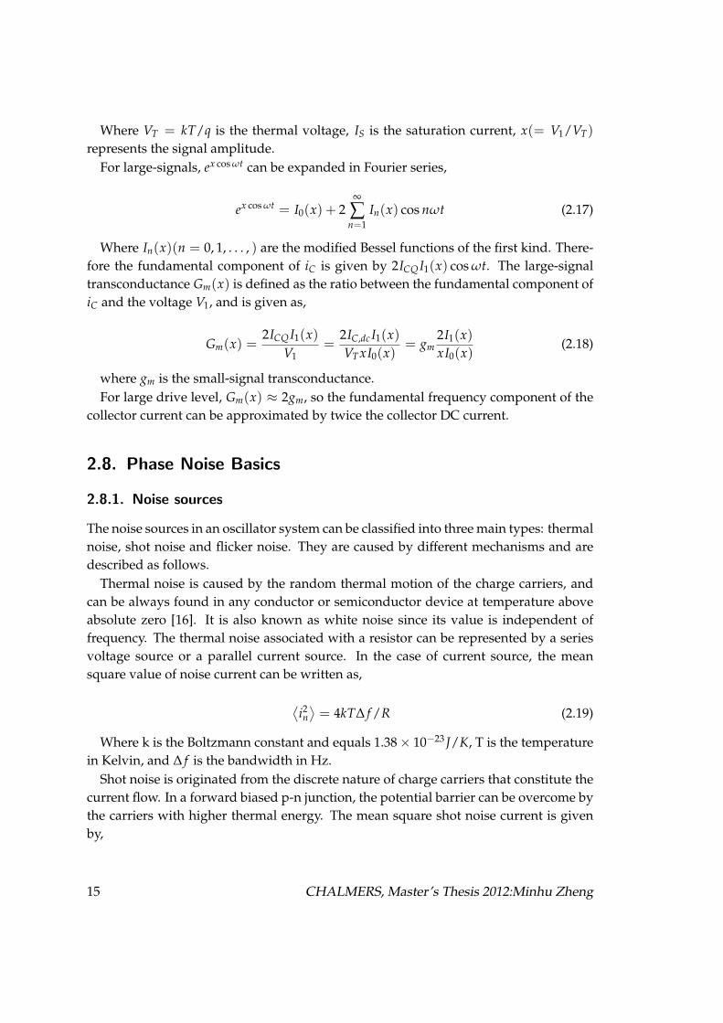
The harmonic balance test bench for the balanced Colpitts is shown in Figure3.5. The tank and the active device were designed in different sub circuits andconnected by a differential OscPort2.
The configuration of the harmonic balance simulator needs some special attentionto obtain the correct simulation results. As recommended in the ADS manual, thefundamental oversample parameter should be set larger than 4 for phase noisesimulation. The order parameter in the harmonic balance defines the maximumharmonic index used for simulation. Larger value of order gives more accurateresults but the maximum harmonic frequency should be kept below the limitationof the transistor model to avoid abnormal simulation results.
7. Waveform optimization
During harmonic balance simulation, the time domain collector current wave-form as well as the transistor Ic vs Vce dynamic load line were monitored. Thebase bias voltage and the emitter degeneration resistor were tuned to control thewaveform. The load line was desired to occupy most of the I-V DC curve withoutreaching the saturation region and exceeding the breakdown limitation.
8. Varactor voltage sweep
25 CHALMERS, Master’s Thesis 2012:Minhu Zheng
vout vout2f
vbvc
HarmonicBalance
HB1
NoiseNode[1]="vout"
Oversample[1]=
FundOversample=4
Order[1]=8
Freq[1]=5 GHz
HARMONIC BALANCE
NoiseCon
NC1
NoiseNode[1]=vout2f
CarrierFreq=
HB NOISE CONTROLLER
negR_wTL
X2
Base_L Base_R
Out_L Out_2f Out_R
Emit_FB_REmit_FB_LCol_L Col_R
VAR
VAR1
Vtune=8
Vbb=2.1
Vcc=5
EqnVar
VAR
VAR2
mcv=1.0
mcc=1.0
mcr=1.0
mch=1.0
EqnVar
Options
Options1
MaxWarnings=50
GiveAllWarnings=yes
I_AbsTol=1e-12 A
I_RelTol=1e-6
V_AbsTol=1e-6 V
V_RelTol=1e-6
Tnom=25
Temp=25
OPTIONS
ParamSweep
Sweep1
Step=4
Stop=13.5
Start=1.5
SimInstanceName[6]=
SimInstanceName[5]=
SimInstanceName[4]=
SimInstanceName[3]=
SimInstanceName[2]=
SimInstanceName[1]="HB1"
SweepVar="Vtune"
PARAMETER SWEEP
V_DC
SRC3
Vdc=Vbb V
R
R1
R=1 kOhm
resonator_wTL
X3
Vcc Vtune
Col_L Emit_FB_L Emit_FB_R Col_R
I_Probe
Ic
Tqhbt_res_nicr
Tqhbt_res_nicr1
W1=10 um
L1=10 um
C1
2
Tqhbt_res_nicr
Tqhbt_res_nicr3
W1=10 um
L1=10 um
C1
2OscPort2
OscP1
MaxLoopGainStep=
FundIndex=1
Steps=10
NumOctaves=2
Z=1.1 Ohm
V=
I_Probe
Idc
V_DC
SRC2
Vdc=Vtune V
V_DC
SRC1
Vdc=Vcc V
Tqhbt_res_nicr
Tqhbt_res_nicr2
W1=10 um
L1=10 um
C1
2
Figure 3.5. Harmonic balance test bench for the balanced Colpitts VCO
The varactor′s C-V curve was first simulated by sweeping the reverse bias voltagefrom 0 V to 14 V. The tuning characteristic of the varactor is presented in Figure3.6. A capacitance ratio of 2 can be obtained between 1.5 V and 13.5 V tuningvoltages. Proper varactor size was chosen depending on the tuning range re-quirement. The fixed capacitors (the one in parallel with the tank inductor in theColpitts and the one in series with the tank inductor in the Clapp) ware replacedby the varactors, and harmonic balance simulation was performed for each tun-ing voltage. If abnormal increase in the phase noise at any tuning voltage wasobserved, step 5 should be checked for the entire tuning range. Design parame-ters were tuned to obtain a phase noise performance with flat frequency response.
9. Design parameter optimization
The effect of various design parameters on phase noise was studied. These in-clude: transistor biasing current density, emitter degeneration inductor value,feedback capacitor ratio and value, varactor arrangement. Details of this sectioncan be found in the following sub chapters.
10. Layout generation and momentum simulation
The layout was generated in this step, and the schematic with layout parasiticelements was re-simulated. Normally the simulation results will change due to
CHALMERS, Master’s Thesis 2012:Minhu Zheng 26

2 4 6 8 10 120 14
2.500p
3.000p
3.500p
4.000p
4.500p
5.000p
5.500p
2.000p
6.000p
Vtune [V]
Cv
C1p5
C13p5
C1p5indep(C1p5)=plot_vs(Cvar, Vtune)=4.403pfreq=14.00000 Hz
1.500 C13p5indep(C13p5)=plot_vs(Cvar, Vtune)=2.352pfreq=14.00000 Hz
13.50
Figure 3.6. The C-V characteristic of a 100µm× 100µm square varactor
the introduction of the parasitic and one should return to the design procedurefrom step 3 to 7.
For the critical parts of the circuit, for example the tank inductor, momentumsimulator was employed. Momentum is the built-in 2.5D EM simulation engine inADS and can simulate the passive structures in the planar technology accurately.
The above design procedures were performed in an iterative manner.
3.3. Design Parameters Optimization
3.3.1. Tank quality factor
According to Leesons theory [17], the most obvious way to improve oscillator phasenoise is by increasing the signal power and utilizing a high Q resonator. While theformer method is straightforward, one can improve the resonator Q considerably bycareful design and optimization. In most cases, the total tank Q factor is limited by theinductor and the varactor.
The electrical model of an inductor is presented in Figure 3.6, where RS and RP repre-
27 CHALMERS, Master’s Thesis 2012:Minhu Zheng

sent the equivalent series and parallel resistance. The Q factor of an inductor is definedas,
Q =ωLRS
(3.1)
And RS is given by,
RS =ρ · l
w · δ · (1− e−t/τ)(3.2)
Where ρ is the resistivity of the metal, l and w are the length and width of the induc-tor, respectively, δ is skin depth and t is the metal thickness.
From the above equation, one can observe that the inductor with thicker metal tendsto have smaller series resistance and therefore offers a higher Q. In the designs, two-metal-stack microstrip lines with a total thickness of 6 µm were implemented as thetank inductors.
Spiral inductors are normally utilized in RFIC designs since the combination of theself inductance and the mutual inductance makes it possible to obtain an inductanceup to several nH at RF frequencies. However, spiral inductors are notorious for theirlow Q factors. Even with technology evolution and careful optimization, inductor Q isstill in the order of 10 at 5 GHz [15].
For microwave applications, transmission lines are preferred since their relativelyhigh Q. A short circuited transmission line has an equivalent inductance given by[24],
L =Z0
2π ftan(βl) (3.3)
Where Z0 is the characteristic impedance of the transmission line, f is the operatingfrequency, β is the phase constant and l is the transmission line length. It should benoted that a transmission can be regarded as an inductor only when its electric lengthis small.
Transmission lines with widths of 200µm and 100µm were implemented in the Clappand Colpitts designs respectively.
In a similar way, to increase the Q factor of a varactor, the series resistance shouldbe minimized. This can be accomplished by introducing the finger varactor structurewhich reduces the sub collector losses [21]. The layouts of a conventional square varac-tor and a 5-finger varactor are shown in Figure 3.7.
3.3.2. Bias Current Density
The bias current density (JC) can affect the transistor cutoff frequency and ft reducesat high current density and the flicker noise is proportional to JC. For the aim of seek-ing for the optimum current density, single-ended Clapp oscillator was tested with 9
CHALMERS, Master’s Thesis 2012:Minhu Zheng 28

Figure 3.7. The layout of square and finger varactors
different current densities not exceeding 30kA/cm2 according to the foundry designmanual.
In order to isolate the JC effect on phase noise, design parameters in Table 3.2 werefixed. At the same time, the ratio of resistors divider R1 and R2 and the area of HBT arevaried to obtain different JC.
The simulation results are plotted in Figure 3.8. As can be seen, the phase noise hasover 1 dB variation for different current densities and the best phase noise was obtainedat JC around 10kA/cm2.
Similar results were observed for a single-ended Colpitts oscillator and one can there-fore conclude that the optimum JC is topology irrelevant.
3.3.3. Transistor Arrangement
The foundry process has unit HBT cell with emitter finger number ranging from 1 to3. To realize larger total device area, multiple transistor unit cells are connected inparallel, and one can have different combinations of emitter finger number, unit emitterlength and width, and transistor number for the same device area. The choice should bemade taking into account of layout convenience and thermal stability. Here the effectof transistor arrangement on phase noise was evaluated on transistors with differentnumber of emitter fingers and unit emitter length (UEL). Table 3.3 lists 12 differenttransistor arrangements employed in the simulation.
To isolate the transistor arrangements effect on phase noise, the optimization wasperformed on a 5 GHz fixed frequency oscillator with a collector current of 80 mA anda current density of 9kA/cm2, in other words, the total emitter area is 900µm2.
29 CHALMERS, Master’s Thesis 2012:Minhu Zheng

-117.0
-116.5
-116.0
-115.5
-115.0
-114.5
PN
@1
00
k [
dB
c/H
z]
Jc [kA/cm2]
Figure 3.8. Phase noise versus bias current density for single-ended Clapp
No. of fingers 1 2 3UEL(µm) 10 15 30 50 10 15 30 50 10 15 30 50No. of HBTs 30 20 10 6 15 10 5 3 10 6 3 2
Table 3.3. List of different transistor arrangements
The phase noise simulation results are shown in Figure 3.9. As can be seen from thefigure, fewer finger transistors with smaller emitter length present superior phase noiseand the variation can be more than 1 dB for different configurations. However, 1 fingertransistor with small emitter length would be impractical from the layout point of viewand should be discarded.
When the transistor is operating under large collector current condition, self heatingbecomes prominent and the temperatures of all the emitter fingers increase. For the3-finger case, the center finger becomes hotter than the two outer ones. This results anon-uniform current distribution in which the center finger carries substantial portionof the total current, and will eventually cause stability issues [25]. Therefore, to ensurethermal stability and make the design robust, 2-finger transistors with a UEL of 15µmwere employed in the designs.
3.3.4. Feedback Capacitor Ratio and Value
The feedback capacitor ratio is believed to be a vital design parameter in Colpitts-likeoscillators. The rule of thumb is a capacitor ratio of 1:4 will result the optimum phase
CHALMERS, Master’s Thesis 2012:Minhu Zheng 30

Figure 3.9. Phase noise simulation results for different transistor arrangements
noise and theoretical support was proposed by Lee and Hajimiri with their LTV model[14]. The transistors base-emitter (gate-source) capacitances are generally neglectedin most designs; however for microwave frequency oscillators the feedback capacitorsbecome comparable with the intrinsic capacitors of the transistor, a different ratio isexpected. Moreover, the optimum capacitive divider ratio is also determined by thetechnology involved and bipolar transistors generally exhibit a smaller ratio than FETs.It has been shown in [26] that for an InGaP HBT process, the ratio of 1:1.5 providesthe best phase noise. Here similar optimization procedures were performed in thiscommercial HBT process to find the optimum capacitor ratios for both the Colpitts andClapp designs.
For the Colpitts oscillator, the feedback capacitors are in parallel with the varactors,and therefore the equivalent tank capacitor the sum of them. For this reason, the de-tailed capacitor value should not be chosen arbitrarily and is given by the tuning rangerequirement.
Three capacitor ratios were investigated for the Colpitts oscillator, and the simulationresults are shown in Figure 3.10. As can be seen, the best phase noise occurs at thecapacitor ratio of 1:1.
For the Clapp oscillator, the feedback capacitors are in series with the varactors, and ifthe capacitance of the varactor is much smaller than that of the feedback capacitors, theequivalent capacitance can be approximated by the varactor. Apart from the capacitorratio, the effect of feedback capacitor values on phase noise was also investigated.
The capacitor values were swept from 6pF to 16pF with 2pF step, and C1 and C2
were assumed to be equal for simplicity. The simulation results are plotted in Figure
31 CHALMERS, Master’s Thesis 2012:Minhu Zheng

-112
-111
-110
-109
-108
-107
-106
-105
1:1 1:1.5 1:2
PN
@ 1
00
kH
z (
dB
c/H
z)
Capacitor divider ratio
Figure 3.10. Phase noise of the Colpitts oscillator versus feedback capacitor ratio
3.11. As can be seen, the phase noise reduces monotonically until the capacitancesreach 14pF. However, a 14pF MIM capacitor is too large to be used in the layout and alarge capacitor exhibits lower self resonant frequency which could limit its applicationat microwave frequencies. Therefore, 12pF is considered to be the optimum value forthe feedback capacitors, which corresponds to an equivalent capacitance of 6pF.
Next, the capacitor ratio effect on Clapp topology was investigated. Five ratios werechosen, keeping the equivalent capacitor to be 6pF. The phase noise simulation resultsare presented in Figure 3.12. As shown in the plot, best phase noise is observed at theratio 0.8:1, however, a ratio below 1:1 would make the oscillator hard to startup at lowtemperature operation. Therefore, a 1:1 capacitor ratio was considered to be optimum,which agrees with the Colpitts topology.
3.3.5. Varactor Bias Choke
The varactor bias choke was utilized to isolate the DC supply and the RF signal onthe varactor. It should present sufficient high impedance at the center frequency of theVCO. The RF choke can be implemented by a quarter wavelength transmission lineor a large inductor. While quarter wavelength transmission lines are too long to beintegrated in the MMIC chip, the spiral inductors were utilized in the designs.
CHALMERS, Master’s Thesis 2012:Minhu Zheng 32

-120.0
-118.0
-116.0
-114.0
-112.0
-110.0
PN
@1
00
k [
dB
c/H
z]
C1, C2 (pF)
Figure 3.11. Phase noise of the Clapp oscillator versus feedback capacitor values
3.4. Simulation Results
The simulation results for the two designs are illustrated here. These include the fre-quency tuning characteristic, the output power with respect to tuning voltage, SSBphase noise spectrum and specifically at 100 kHz offset, the IC vs. VCE loadline andthe time domain waveform of IC and VCE.
3.4.1. Balanced Colpitts VCO
The simulation results of the balanced Colpitts VCO is shown in Figure 3.13. As canbeen seen, the balanced Colpitts VCO shows oscillation frequencies ranging from 4.8GHz to 5.4 GHz when the tuning voltage is swept from 1.5 V to 13.5 V. The fundamentaloutput power is larger than 3 dBm throughout the tuning range. The VCO has a phasenoise as low as -110 dBc/Hz at 100 kHz offset, exhibiting a 3 dB variation with respect totuning voltage. The time domain waveform of VCE and IC together with the dynamicloadline were also plotted and the narrow IC pulse translates to low phase noise asindicated in [14] [23].
3.4.2. Balanced Clapp VCO
The simulation results of the balanced Clapp VCO is shown in Figure 3.14. The bal-anced Clapp VCO shows a fundamental oscillation frequency ranging from 4.7 GHzand 5.5 GHz and output power more than 1 dBm for different tuning voltages. Dueto the much higher current excitation than the balanced Colpitts VCO, the balancedClapp VCO is believed to further improve phase noise level according to both LTI[17]
33 CHALMERS, Master’s Thesis 2012:Minhu Zheng

-118
-116
-114
-112
-110
0.8:1 1:1 1.3:1 1.5:1 1.8:1
PN
@ 1
00
kH
z (
dB
c/H
z)
Capacitor ratio
Figure 3.12. Phase noise of the Clapp oscillator versus feedback capacitor ratio
and LTV[14] models. The HB simulation shows a 100 kHz phase noise as low as -122dBc/Hz, which is more than 10 dB superior to that of the balanced Colpitts. The timedomain waveform of VCE and IC, and the dynamic loadline were plotted as well. How-ever, the loadline is distinct from the balanced Colpitts case and little information canbe extracted from it.
3.4.3. Summary and Discussion
To benchmark VCOs with different oscillation frequencies and tuning ranges, the nor-malized figure of merit with tuning range (FOMT) is utilized. FOMT is given by,
FOMT = L (∆ω)− 20 · log(( ω0
∆ω
)·(
FTR10
))+ 10 · log
(Pdiss
1mW
)(3.4)
Where L (∆ω) is the phase noise at offset frequency ∆ω, ω0 is the center oscillationfrequency, Pdiss is the power dissipation, and FTR is the tuning range of the VCO.
The simulation results of these two topologies are summarized in Table 3.4 withFOMT calculated as well.
As can be seen from the table, both topologies meet the frequency and tuning rangespecifications, while the balanced Clapp VCO presents 5% more tuning bandwidth. Asfar as the phase noise is concerned, the balanced Clapp VCO is roughly 11dB superiorfor different tuning voltages. The balanced Clapp VCO consumes approximately 4times DC power of that of the balanced Colpitts VCO. Taking into consideration of allthe factors, the balanced Clapp VCO shows 9dB better FOMT.
CHALMERS, Master’s Thesis 2012:Minhu Zheng 34

Balanced Clapp Balanced ColpittsFrequency 4.71∼5.55GHz 4.84∼5.40GHzTuning Range 16.3% 11%Phase Noise @ 100kHz -119.6 ∼ -122.2 dBc/Hz -108.7 ∼ -111.2 dBc/HzOutput Power 1.1 ∼ 5.5dBm 3.2 ∼ 6.4dBmPower Dissipation 607 ∼ 755mW 161 ∼ 195mWFOMT(averaged) -191.0 dBc/Hz -182.5dBc/Hz
Table 3.4. Summary of simulation results of two VCOs
The superior phase noise obtained from balanced Clapp VCO is partly owing to itshigh current operation while its Colpitts counterpart can only operates at small currentcondition. [13], [18] point out that low tank impedance is favorable in low phase noiseVCO designs and the solution for balanced Colpitts VCO is to use a tank inductor assmall as possible. The Clapp topology, however, can achieve a much smaller equiva-lent tank impedance than that of the Colpitts; thereby allowing higher current beinginjected into the tank while still not exceeding the technologys breakdown limitation.The equivalent tank impedance for both topologies is derived in Appendix A.
Since the design phase thesis was pure simulation based and no tape-out plan wasscheduled. One may easily question the validity of the simulation results, especially thephase noise results. As has been discussed in Chapter 2, the accuracy of phase noisesimulation results depends mostly on the accuracy of the transistor noise source model-ing and the way in which CAD tools characterize the low frequency noises. However,at 100kHz offset frequency, flicker noise, which is not modeled as cyclostationary inmost CAD tools, has little contribution on the phase noise. Therefore small discrepancybetween the simulation and measurement results is expected. This assumption hasbeen proved true by tape-outs in the prior version of the current commercial foundryprocess. The simulation and measured phase noise is plotted in Figure 3.15. As can beseen, the HB simulator generally overestimates the phase noise by 3-5 dB at 100 kHzoffset frequency for different tuning voltages while at 10 kHz offset it underestimatesthe phase noise by up to 10 dB.
35 CHALMERS, Master’s Thesis 2012:Minhu Zheng

2 4 6 8 10 120 14
4.9
5.0
5.1
5.2
5.3
5.4
4.8
5.5
Vtune [V]
Fre
quency [G
Hz]
fmin
fmax
Frequency vs. Vtune
fminVtune=HB.freq[1]=4.844G
1.500
fmaxVtune=HB.freq[1]=5.401G
13.50
(a) Frequency vs. Vtune
2 4 6 8 10 120 14
2
4
6
8
0
10
Vtune [V]
Pow
er
[dB
m]
Fundamental Output Power vs. Vtune
(b) Fundamental Output Power vs. Vtune
1.000k 10.00k 100.0k 1.000M100.0 10.00M
-140
-120
-100
-80
-60
-160
-40
noisefreq, Hz
SS
B P
ha
se
No
ise
[d
Bc/H
z]
SSB Phase Noise Fundamental
(c) SSB Phase Noise Fundamental Frequency
2 4 6 8 10 120 14
-110
-105
-115
-100
Vtune [V]
SS
B P
ha
se
No
ise
[d
Bc/H
z]
pn
Phase Noise @ 100 kHz vs. Vtune
pnVtune=vout.pnmx[3]=-111.2
1.5
(d) Phase Noise @ 100 kHz vs. Vtune
1 2 3 4 5 6 7 8 90 10
-20.00m
0.0000
20.00m
40.00m
60.00m
80.00m
100.0m
120.0m
-40.00m
140.0m
Vce [V]
Ic [A
]
Ic vs. Vce Loadline
(e) Ic vs. Vce Loadline
50 100 150 200 250 300 350 4000 450
-20
0
20
40
60
80
100
-40
120
1
2
3
4
5
0
6
time, psec
ts(I
c.i),
mA
Vce
Ic Vce Time Domain Waveform
(f) Ic Vce Time Domain Waveform
Figure 3.13. Simulation results of the balanced Colpitts VCO.
CHALMERS, Master’s Thesis 2012:Minhu Zheng 36

4 6 8 10 12 142 16
4.8
5.0
5.2
5.4
4.6
5.6
Vtune [V]
Fre
quency [G
Hz]
fmin
fmaxFrequency vs. Vtune
fminVt=freq[1]=4.708G
2.000
fmaxVt=freq[1]=5.554G
15.00
(a) Frequency vs. Vtune
4 6 8 10 12 142 16
0
2
4
6
8
-2
10
Vtune [V]
Pow
er
[dB
m]
Fundamental Output Power Vs. Vtune
(b) Fundamental Output Power vs. Vtune
1.000k 10.00k 100.0k 1.000M100.0 10.00M
-160
-140
-120
-100
-80
-60
-180
-40
noisefreq, Hz
SS
B P
ha
se
No
ise
[d
Bc/H
z]
SSB Phase Noise Fundamental
(c) SSB Phase Noise Fundamental Frequency
4 6 8 10 12 142 16
-123
-121
-119
-117
-125
-115
Vtune [V]
SS
B P
ha
se
No
ise
[d
Bc/H
z]
pn
Phase Noise @ 100 kHz Vs. Vtune
pnVt=pnmx[3]=-122.252
7.000
(d) Phase Noise @ 100 kHz vs. Vtune
1 2 3 4 5 6 7 8 90 10
-100.0m
0.0000
100.0m
200.0m
300.0m
400.0m
500.0m
-200.0m
600.0m
Vce [V]
Ic [A
]
Ic vs. Vce Loadline
(e) Ic vs. Vce Loadline
50 100 150 200 250 300 350 4000 450
-100
0
100
200
300
-200
400
1
2
3
4
5
6
0
7
time, psec
Vce
ts(I
c1.i),
mA
Ic Vce Time Domain Waveform
(f) Ic Vce Time Domain Waveform
Figure 3.14. Simulation results of the balanced Clapp VCO.
37 CHALMERS, Master’s Thesis 2012:Minhu Zheng

-130.00
-120.00
-110.00
-100.00
-90.00
-80.00
-70.00
-60.00
0 2 4 6 8 10 12 14 16
SS
B P
ha
se N
ois
e [d
Bc/
Hz]
Tuning Voltage [V]
SSB Phase Noise vs. Tuning Voltage
simulated(10kHz offset)
measured(10kHz offset)
simulated(100kHz offset)
measured(100kHz offset)
Figure 3.15. Typical phase noise performance of a VCO designed in previous process
CHALMERS, Master’s Thesis 2012:Minhu Zheng 38

4. Conclusion
The evolution of microwave point-to-point radio, towards higher order modulationschemes, is continuously posing more stringent requirement on the signal generatingunits of the system, the VCOs. Therefore, to design a low-cost and compact MMICVCO is of great research value.
The study began by reviewing basic theory of oscillator systems, which followedby comparing various resonator and active device technologies, as well as topologiesemployed in VCO designs. Small signal and large signal analysis of a simple oscillatorwere carried out for illustrative purpose. Noise modeling of HBT was briefly describedand two analytical phase noise models, Leeson’s LTI model and Hajimiri’s LTV modelwere presented. CAD tools with HB simulator can facilitate the design of VCOs to agreat extent. The principle of HB simulation was introduced and the limitation of theHB simulators in terms of making accurate phase noise prediction was mentioned.
ADS with a commercial InGaP HBT process design kit was employed to design twoMMIC VCOs with different topologies, balanced Colpitts and balanced Clapp. Thedesign followed a systematic procedure in an iterative manner. Various design param-eters affecting phase noise performance were studied and both VCOs were optimizedfor the best phase noise performance. Simulation results show that the balanced ClappVCO is superior in terms of both absolute phase noise value and FOMT, at an expenseof high power consumption. On the other hand, balanced Colpitts VCO can operateunder lower current condition while still offering moderate phase noise. The validityof the simulation results was verified by comparing simulation and measured resultsfrom a VCO designed with the previous version of this process.
39 CHALMERS, Master’s Thesis 2012:Minhu Zheng

CHALMERS, Master’s Thesis 2012:Minhu Zheng 40

5. Future Work
Despite its inferior phase noise performance, the balanced Colpitts VCO still benefitsfrom its low current operation and thus is more power efficient. Moreover, improve-ment in phase noise, 3dB in theory, can be achieved by coupling two identical VCOstogether using injection locking techniques. Two extra merits are expected from thistopology. First the redundancy makes the product more reliable, e.g. once any of thetwo VCOs fails, the other one still keeps the system running. Second, with proper de-signed power management circuit, one of the VCO units can be switched off undercertain circumstances; thereby reducing the power consumption and making the prod-ucts more environmentally friendly.
Attempts to include the idea of injection locking were made using the transient sim-ulation. However, due to time constraints, little progress has been achieved. The inves-tigation on injection locking would be a good extension of this work.
Since the design task was based on computer simulations, the results obtained arenot totally convincing. Funding permitting, tape-outs and measurements of the twoVCOs would further complement this work.
41 CHALMERS, Master’s Thesis 2012:Minhu Zheng
CHALMERS, Master’s Thesis 2012:Minhu Zheng 42

References
[1] A.P.S. Khanna. Microwave Oscillators: The State of the Technology. MicrowaveJournal, Apr 2006.
[2] S. Little. Is Microwave Backhaul Up to the 4G Task? IEEE Microwave Magazine,pages 67–74, Aug 2009.
[3] J. Hansryd and J. Edstam. Microwave capacity evolution. Ericsson Review, 2011.
[4] G.Gonzalez. Foundations of Oscillator Circuit Design. Artech House, Boston, 2007.
[5] C.W. Nelson, D.A. Howe, and A. Gupta. Ultra-low Noise Cavity-stabilized Mi-crowave Reference Oscillator Using an Air-dielectric Resonator. In Proceedings ofthe 36th Annual PTTI Meeting, pages 173–178, Dec 2004.
[6] A.P.S. Khanna. Review of Dielectric Resonator Oscillator Technology. In 41st An-nual Symposium on Frequency Control, pages 478 – 486, 1987.
[7] Hittite Microwave Corporation. Dielectric Resonator Oscillator (DRO) Module,8.0 - 8.3 GHz.
[8] M. Loboda G. Montress, T. Parker and M. Greer. Extremely Low Phase-noise SAWResonators and Oscillators: Design and Performance. IEEE Trans. on UltrasonicsFerroelectrics and Frequency Control, 35(6):657–667, Nov 1988.
[9] A.P.S. Khanna, E. Gane, T. Chong, H. Ko, P. Bradley, R. Ruby, and J.D. Larson.A Film Bulk Acoustic Resonator (FBAR) L-band Low Noise Oscillator for DigitalCommunications. In Proc. 32nd European Microwave Conference, 2002.
[10] X. Gao, M. Koechlin, C.Lyons, J. Chiesa, G. Guven, and P. Katzin. A Low Noise9.95/10.66 GHz PLO for Optical Applications. In IEEE MTT-S International Sympo-sium Digest, volume 2, pages 729–732, 2003.
[11] endwave. 3-11 Ghz Center Frequency YIG Tuned Oscillator.
[12] Schwierz. F and Liou. J J. Rf transistors: Recent Developments and Roadmaptoward Terahertz Applications. Solid-State Electronics, pages 1079–1091, 2007.
43 CHALMERS, Master’s Thesis 2012:Minhu Zheng

[13] G.Gonzalez. Microwave Transistor Amplifiers Analysis and Design. Prentice Hall,New Jersery, 2nd edition, 1997.
[14] A.Hajimiri and T.H.Lee. A General Theory of Phase Noise in Electrical Oscillators.IEEE Journal of Solid-State Circuits, 33(2):179–194, 1998.
[15] B.Razavi. RF Microelectronics. Prentice Hall, 2nd edition, 2011.
[16] A.Grebennikov. RF and Microwave Transistor Oscillator Design. John Wiley & Son,Chichester, 2007.
[17] D.B.Leeson. A Simple Model of Feedback Oscillator Noise Spectrum. in Proc IEEE,54:329–330, Feb 1966.
[18] I.D. Robertson and S. Lucyszyn, editors. RFIC and MMIC Design and Technology.The Institution of Engineering and Technology, London, 2001.
[19] C. Gourdon, J.-C. Nallatamby, D. Baglieri, M. Prigent, M. Camiade, and J. Obregon.Accurate Design of HBT VCOs with Flicker Noise Up-conversion Minimization,Using an Advanced Low-Frequency Cyclostationary Noise Model. In MicrowaveSymposium Digest, 2005 IEEE MTT-S International, pages 1519–1522, Jun 2005.
[20] P.A Traverso, C. Florian, M. Borgarino, and F. Filicori. An empirical bipolar devicenonlinear noise modeling approach for large-signal microwave circuit analysis.IEEE Transactions. MTT, 54(12):4341–4352, Dec 2006.
[21] H.Zirath, R.Kozhuharov, and M.Ferndahl. Balanced Colpitt Oscillator MMICs De-signed for Ultra-Low Phase Noise. IEEE J.solid-state circuits, 40(10), 2005.
[22] Sonja R. Nedeljovic, John R. McMacken, Paul J. Partyka, and Joseph M. Gering. ACustom III-V Heterojunction Bipolar Transistor Model. Microwave Journel, pages60–84, Apr 2009.
[23] S.Lai, D.Kuylenstierna, I.Angelov, B.Hansson, R.Kozhuharov, and H.Zirath. Gm-boosted balanced Colpitts compared to conventional balanced Colpitts and cross-coupled VCOs in InGaP HBT technology. In IEEE Asia-Pacific Microwave Confer-ence, 2010.
[24] A I.Khalil and P.Katzin. A low power high performance 4GHz SiGe HBT VCO.Microwave Symposium Digest, pages 1505–1508, 2004.
[25] F.Schwierz and J J Liou. Modern Microwave Transistors: Theory, Design, and Perfor-mance. John Wiley & Sons, New Jersery, 2003.
CHALMERS, Master’s Thesis 2012:Minhu Zheng 44

[26] D.Kuylenstierna, S.Lai, M.Bao, and H.Zirath. Design of Low-Phase Noise Oscil-lators and Wideband VCOs in InGaP HBT Technology. IEEE Transactions, MTT,60:3420 – 3430, Nov 2012.
45 CHALMERS, Master’s Thesis 2012:Minhu Zheng

CHALMERS, Master’s Thesis 2012:Minhu Zheng 46

A. Equivalent Tank Impedance
The tank circuit of a Clapp oscillator is shown in Figure A.1.
C1
C2 Re
Cv
L
Leff
Figure A.1. Equivalent tank inductance of a Clapp oscillator
The oscillation frequency is given by,
ωosc =1√
LCtot(A.1)
Where,
1Ctot
=1
C1+
1C2
+1
CV(A.2)
For small CV , Ctot can be approximated by CV . The series combination of the tankinductor and the varactor is inducive at oscillation frequency, and the effective induc-tance Le f f is given by,
jωoscLe f f = jωoscL− 1jωoscCV
(A.3)
If we define the resonant frequency of the series LC network as ω′osc,
47 CHALMERS, Master’s Thesis 2012:Minhu Zheng

ω′osc =1√LCV
(A.4)
So Le f f can be expressed as,
Le f f = L(
1− ω′2oscω2
osc
)(A.5)
Since Ctot can be approximated by CV , ω′osc is therefore very close to ωosc, this makesthat the effective tank impedance much smaller that the impedance of the inductoritself.
In comparison, let us also consider the Colpitts oscillator. The tank circuit of a Col-pitts oscillator is shown in Figure A.2.
C1
C2Re
CVL Leff
Figure A.2. Equivalent tank inductance of a Colpitts oscillator
The derivation of effective tank impedance is similar as that for the Clapp oscillator.The oscillating frequency is given by,
ωosc =1√
LCtot(A.6)
Where Ctot can be written as,
Ctot =C1 + C2
C1C2+ CV (A.7)
So Ctot is larger than CV , and the effective inductance of the parallel tank is given as,
jωoscLe f f =1
jωoscCV +1
jωoscL
(A.8)
CHALMERS, Master’s Thesis 2012:Minhu Zheng 48

The resonant frequency of the parallel LC network is,
ω′osc =1√LCV
(A.9)
Finally the effective inducatance can be rewrote as,
Le f f =L
1− ω2osc
ω′2osc
(A.10)
and is larger than the original tank inductance.
49 CHALMERS, Master’s Thesis 2012:Minhu Zheng