influence of atomic tip structure on the intensity of ... of atomic tip... · physical review b...
TRANSCRIPT

PHYSICAL REVIEW B 93, 165415 (2016)
Influence of atomic tip structure on the intensity of inelastic tunneling spectroscopy data analyzedby combined scanning tunneling spectroscopy, force microscopy, and density functional theory
Norio Okabayashi,1,2,* Alexander Gustafsson,3 Angelo Peronio,1 Magnus Paulsson,3 Toyoko Arai,2 and Franz J. Giessibl11Institute of Experimental and Applied Physics, University of Regensburg, D-93053 Regensburg, Germany
2Graduate School of Natural Science and Technology, Kanazawa University, 920-1192 Ishikawa, Japan3Department of Physics and Electrical Engineering, Linnaeus University, 391 82 Kalmar, Sweden(Received 31 March 2015; revised manuscript received 3 March 2016; published 13 April 2016)
Achieving a high intensity in inelastic scanning tunneling spectroscopy (IETS) is important for precisemeasurements. The intensity of the IETS signal can vary by up to a factor of 3 for various tips without anapparent reason accessible by scanning tunneling microscopy (STM) alone. Here, we show that combining STMand IETS with atomic force microscopy enables carbon monoxide front-atom identification, revealing that highIETS intensities for CO/Cu(111) are obtained for single-atom tips, while the intensity drops sharply for multiatomtips. Adsorption of the CO molecule on a Cu adatom [CO/Cu/Cu(111)] such that the molecule is elevated over thesubstrate strongly diminishes the tip dependence of IETS intensity, showing that an elevated position channelsmost of the tunneling current through the CO molecule even for multiatom tips, while a large fraction of thetunneling current bypasses the CO molecule in the case of CO/Cu(111).
DOI: 10.1103/PhysRevB.93.165415
Inelastic electron tunneling spectroscopy (IETS) with scan-ning tunneling microscopy (STM) is an effective method toanalyze the vibrational modes of a single adsorbed moleculewith subnanometer lateral resolution [1,2]. The vibrationalenergy of a molecule on a substrate strongly depends onthe surrounding environment, such as the substrate structureand composition [3]. By studying these subtle changes ofthe vibrational energy using STM-IETS with a molecular-functionalized tip, it has been demonstrated that STM-IETScan provide information on the inner structure of a molecule[4,5] similarly to atomic force microscopy (AFM) [6]. Theseadvantages of STM-IETS have accelerated research in relatedfields [7–16]. Owing to recent progress in the theoreticaldescription of IETS [17–22], the qualitative understandinghas been improved considerably: the symmetry of the wavefunctions of a tip and a molecule on a substrate and avibrational mode of the molecule are predicted to influencethe efficiency of the inelastic process (γinel) for the tunnelingcurrent involving the molecule. In order to discuss γinel on thebasis of the intensity of IETS, we have to consider that IETSintensity is described by the multiplication of two factors: (1)the ratio of the tunneling current passing through a molecule tothe total tunneling current (Imolecule/Itotal) and (2) the efficiencyof the inelastic process (γinel). These factors should in principlebe affected by the geometrical structure of the substrate and ofthe tip.
The geometrical structure of a metal tip apex can bedetermined by using carbon monoxide (CO) front-atomidentification (COFI) provided by AFM [23,24], where the tipapex of a force sensor is probed by a CO molecule that standsupright on a metal surface [inset of Fig. 1(e)]. The metallic tipapex atom has a dipole moment induced by the Smoluchowskieffect [25], whose direction is the same as that of the COmolecule adsorbed on the surface [26]. Thus in the distanceregime where the electrostatic interaction between the tip andthe molecule dominates, the force between them is attractive.
When the tip is scanned over the CO molecule, this attractiveforce appears as a dip (smaller value) in the frequency-shiftimage for each atom at its apex, i.e., the number of the attractiveforce minima provides the number of atoms composing the tipapex [27].
In this paper, we have investigated the tip-structure-dependent IETS for individual CO molecules on a Cu surfaceby combining STM and AFM. We have found that a tip with asingle atom on its apex (single-atom tip) gives a stronger IETsignal compared with a blunt tip consisting of four atoms on theapex (four-atom tip) for a CO molecule on a Cu(111) surface.However, the intensities of the two tips become comparablewhen a Cu adatom is inserted between the CO molecule andthe Cu(111) substrate. From these findings, we will discussthe inelastic efficiency (γinel) as dependent on the geometry ofthe opposite electrode, and demonstrate the validity of modernIETS theory.
The experiments were carried out in an ultrahigh-vacuumlow-temperature (LT) (4.4 K) combined STM and AFM(LT-STM/AFM, Omicron Nanotechnology, Taunusstein, Ger-many). A Cu(111) surface was cleaned by repeated sputteringand annealing before CO molecules were adsorbed on it. Theforce acting between a CO molecule and the apex of themetallic tip was measured by a qPlus sensor [28]. The sensor,whose stiffness is k = 1800 N/m, oscillates at f0 = 47375 Hzwith a constant amplitude of 20 pm during all STM/AFMmeasurements. When an average force gradient 〈kts〉 actsbetween the tip and the CO molecule, the sensor frequency isshifted by �f = f0〈kts〉/2k [29]. The current 〈It〉 is averagedfor many cycles of the sensor oscillation, since the bandwidthof the current amplifier is small compared to f0. In order tomeasure the conductance (dI /dV ) and IET signal (d2I/dV 2),a modulation voltage (2338.7 Hz, 1 mVrms) is added to thesample bias and the first and second harmonics in the currentare detected by a lock-in amplifier (HF2LI, Zurich Instruments,Zurich, Switzerland). Throughout the whole paper, the IETsignal is normalized by the differential conductance, i.e.,IETS = (d2I/dV 2)/(dI/dV ) [10,14,18,20]. The tip is formedfrom an etched tungsten wire, cleaned by field evaporation and
2469-9950/2016/93(16)/165415(6) 165415-1 ©2016 American Physical Society

NORIO OKABAYASHI et al. PHYSICAL REVIEW B 93, 165415 (2016)
FIG. 1. Constant-height current (a) [(c)] and frequency shift (b)[(d)] images (1.5×1.5 nm2) for a CO molecule adsorbed on Cu(111)obtained with a single-atom tip (four-atom tip). The tip height is seton the Cu(111) substrate at a sample bias Vt = −1 mV and an averagecurrent 〈It〉 = 1.5 nA. (e) Normalized IETS for a CO molecule at aset point of Vt = −50 mV and 〈It〉 = 5 nA, where the intensity of theIETS on the Cu(111) surface is subtracted.
repeatedly poked into the Cu substrate to prepare various tipapexes [23,24,30]. The repeated poking processes probablycover the tip apex with Cu atoms. The poking processesalso scatter Cu adatoms on the Cu(111) surface which areemployed as another target by adsorbing a CO molecule andas an opposite electrode for the CO-functionalized tip [31].
Calculations of the IETS are performed with the densityfunctional theory program SIESTA [32]. From the relaxedgeometries obtained by SIESTA, elastic transport propertiesare calculated by attaching electrodes and using TRANSIESTA
[33]. Vibrational frequencies and IETS are obtained from theTRANSIESTA calculations using the postprocessing packageINELASTICA [34]. The SIESTA (TRANSIESTA) calculations utilizea supercell consisting of a 7- (17-) layer thick 4×4 Cuslab together with the CO molecule and a pyramidal tipmodeled by four Cu atoms on the reverse side of the slab. Thecomputations were performed using the following parameters:the Perdew-Burke-Ernzerhof functional, a 400 Ry real spacecutoff, 4 × 4 k-points, and a double zeta, polarization (DZP)[single zeta, polarization (SZP)] basis set for CO (Cu). TheIETS calculations are then performed at the � point.
Figure 1(a) [1(c)] shows a constant-height current image ofa CO molecule on the Cu(111) surface obtained by a single-atom tip (a four-atom tip), as confirmed by the simultaneouslyacquired �f image in Fig. 1(b) [1(d)]. For both tips we seethe dip in the current image at the position of the CO molecule[35,36], where the current on top of the CO molecule is largerfor the four-atom tip than for the single-atom tip owing to thelarger tip area from which electrons can tunnel. Figure 1(e)shows the IETS for CO molecules obtained with the single-atom tip [37] and the four-atom tip, where identical current setpoints are used for both tips. As described in Appendix A, abackground IETS measured on the copper surface is subtractedfrom that on the CO molecule. In the case of the single-atomtip, the frustrated translational (FT; ∼ 4 meV) and frustratedrotational (FR; ∼35 meV) modes of the CO molecule [7–9]are clearly seen in its IETS. However, the IETS intensityacquired with the four-atom tip is considerably smaller thanthat acquired with the single-atom tip: a 65% decrease for
FIG. 2. (a) COFI images (1.5×1.5 nm2) and (b) cross sections ofthe constant-height current images on a CO molecule with differentsingle-atom tips (tips 1–5) at a set point of Vt = −1 mV and 〈It〉 =1.5 nA on the Cu(111) surface. As a reference, the cross section ofthe current image with the four-atom tip in Fig. 1(c) is added in (b).(c) IETS for CO molecules with the same tips where the set point ona CO molecule is Vt = −50 mV and 〈It〉 = 5 nA.
both the FT and FR modes. A reduced IETS intensity is alsoobserved for tips with two and three atoms on their apexes.
The strong intensity of the IETS provided by single-atomtips is confirmed by preparing different tips, which by COFImeasurements [Fig. 2(a)] are single-atom tips. Cross sectionsof constant-height current image are shown in Fig. 2(b) [38].Note that tip 1 is the one used in Figs. 1(a) and 1(b). In the caseof tips 1 through 5, the minimum current acquired on the COmolecules is almost identical and the value is 24% of that on theCu surface; thus these single-atom tips are judged to be sharp.The normalized IETS is also consistent for the different sharpsingle-atom tips (tips 1–5) [Fig. 2(c)] (Appendix A). On theother hand, the IETS intensity with a single-atom tip havingsecondary-atoms outside of the apex which can contribute
FIG. 3. (a) IETS with the single-atom tips (red) and the four-atom tip (blue) for a CO molecule on a Cu adatom. (b) IETS of aCO-functionalized tip for a Cu adatom (red) and the bare Cu(111)surface (blue). In both cases [(a) and (b)], the tip height is set atVt = −50 mV and 〈It〉 = 5 nA at the measurement position.
165415-2
INFLUENCE OF ATOMIC TIP STRUCTURE ON THE . . . PHYSICAL REVIEW B 93, 165415 (2016)
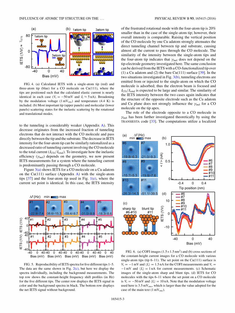
FIG. 4. (a) Calculated IETS with a single-atom tip (red) andthree-atom tip (blue) for a CO molecule on Cu(111), where thetips are positioned such that the calculated elastic current is nearlyidentical in each case (Vt = −50 mV and It ≈ 5 nA). Broadeningby the modulation voltage (1 mVrms) and temperature (4.4 K) isincluded. (b) Most important tip (upper panels) and molecular (lowerpanels) scattering states for the inelastic scattering by the rotationaland translational modes.
to the tunneling is considerably weaker (Appendix A). Thisdecrease originates from the increased fraction of tunnelingelectrons that do not interact with the CO molecule and passdirectly between the tip and the substrate. The decrease in IETSintensity for the four-atom tip can be similarly rationalized as adecreased ratio of tunneling current involving the CO moleculeto the total current (ICO/Itotal). To investigate how the inelasticefficiency (γinel) depends on the geometry, we now presentIETS measurements for a system where the tunneling currentis predominantly passing through a CO molecule.
Figure 3(a) shows IETS for a CO molecule on a Cu adatomon the Cu(111) surface (Appendix A) with the single-atomtips [37] and the four-atom tip used in Fig. 1(e), where thecurrent set point is identical. In this case, the IETS intensity
400-40Bias (mV)
IETS
(1/V
)
0
40
-40
#1
#1
#2
#2
#3
#3
#4
#4
#5
#5
400-40Bias (mV)
400-40Bias (mV)
400-40Bias (mV)
400-40Bias (mV)
IETS
(1/V
) 40
-40
0
#1
-22.9/-7.4
#2
-38.6/-15.3
#3
-59.4/-9.7
#4
-31.0/-9.9
#5
-18.3/-8.6
Δf (Hz) min max
FIG. 5. Reproducibility of IETS spectra for five different tips 1–5.The data are the same shown in Fig. 2(c), but here we display thespectra individually, including the background measurements. Thetop row shows the constant-height frequency shift profiles (in Hz)for the five different tips. The center row displays the IETS signal incolor and the background spectra in black. The bottom row displaysthe net IETS signal without background.
of the frustrated rotational mode with the four-atom tip is 20%smaller than in the case of the single-atom tip; however, theiroverall intensity is comparable. Raising the vertical positionof the CO molecule by one Cu adatom strongly attenuates thedirect tunneling channel between tip and substrate, causingalmost all the current to pass through the CO molecule. Thesimilarity of the intensity between the single-atom tips andthe four-atom tip indicates that γinel does not depend on thetip-electrode geometry investigated here. The same conclusioncan be derived from the IETS with a CO-functionalized tip over(1) a Cu adatom and (2) the bare Cu(111) surface [39]. In thetwo situations investigated in Fig. 3(b), tunneling electrons areemitted from or injected to the single-atom on which the COmolecule is adsorbed; thus the electron beam is focused andICO/Itotal is expected to be large and similar. The similarity ofthe IETS intensity between the two cases again indicates thatthe structure of the opposite electrode such as the Cu adatomand Cu plane does not strongly influence the γinel for a COmolecule on the tip apex.
The role of the electrode opposite to a CO molecule inγinel has been further investigated theoretically by using theTRANSIESTA code [33]. The computations utilize a localized
IETS
(1/V
)
Tip position (nm)
0
1.0
0 0.4-0.4
400-40
0
10
-10
Bias (mV)
(b)
(d)
#6#7#8#9#10#11
0.5
#6#7#8#9#10#11
(a) Δf (Hz)
(c)sharp tip blunt tip
#6
-19.8/-6.3
#7
-21.0/-9.3#8
-15.7/-5.3
#9
-19.8/-7.6#10
-26.3/-14.5
#11
-51.1/-39.5
min max
#11#6-#10
< I>
(nA
)
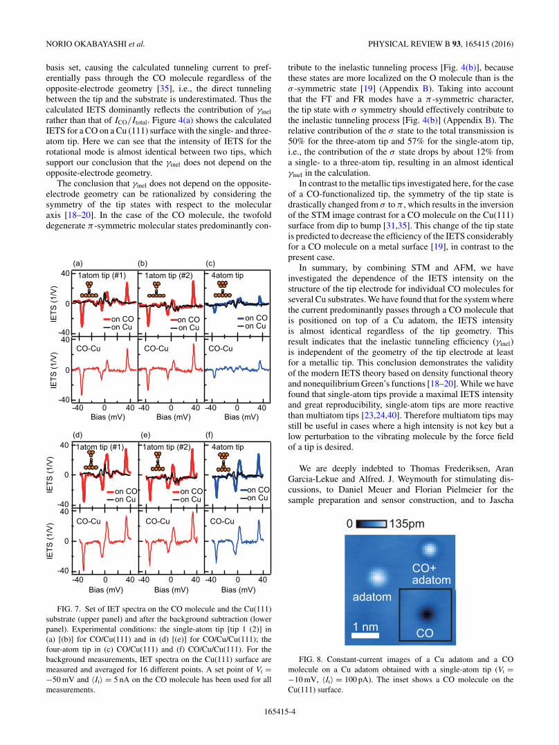
FIG. 6. (a) COFI images (1.5×1.5 nm2) and (b) cross sections ofthe constant-height current images for a CO molecule with varioussingle-atom tips (tip 6–11). The set point on the Cu(111) surface isVt = −1 mV and 〈It〉 = 1.5 nA for the COFI measurements and Vt =−1 mV and 〈It〉 = 1 nA for current measurements. (c) Schematicimages of the single-atom sharp and blunt tips. (d) IETS for COmolecules with the tips 6–11 where the set point on a CO moleculeis Vt = −50 mV and 〈It〉 = 10 nA. Note that the modulation voltageused here is 3.5 mVrms, which is larger than the value adopted for thecase of the main text (1 mVrms).
165415-3
NORIO OKABAYASHI et al. PHYSICAL REVIEW B 93, 165415 (2016)
basis set, causing the calculated tunneling current to pref-erentially pass through the CO molecule regardless of theopposite-electrode geometry [35], i.e., the direct tunnelingbetween the tip and the substrate is underestimated. Thus thecalculated IETS dominantly reflects the contribution of γinel
rather than that of ICO/Itotal. Figure 4(a) shows the calculatedIETS for a CO on a Cu (111) surface with the single- and three-atom tip. Here we can see that the intensity of IETS for therotational mode is almost identical between two tips, whichsupport our conclusion that the γinel does not depend on theopposite-electrode geometry.
The conclusion that γinel does not depend on the opposite-electrode geometry can be rationalized by considering thesymmetry of the tip states with respect to the molecularaxis [18–20]. In the case of the CO molecule, the twofolddegenerate π -symmetric molecular states predominantly con-
Bias (mV)-40 400
Bias (mV)-40 400
Bias (mV)-40 400
Bias (mV)-40 400
Bias (mV)-40 400
Bias (mV)-40 400
IETS
(1/V
)
-40
40
0
IETS
(1/V
)
-40
40
0
IETS
(1/V
)
-40
40
0
IETS
(1/V
)
-40
40
0
1atom tip (#1) 1atom tip (#2) 4atom tip
1atom tip (#1) 1atom tip (#2) 4atom tip
(b) )c()a(
(e) )f()d(
on COon Cu
on COon Cu
on COon Cu
on COon Cu
on COon Cu
on COon Cu
CO-Cu CO-Cu CO-Cu
CO-Cu CO-Cu CO-Cu
FIG. 7. Set of IET spectra on the CO molecule and the Cu(111)substrate (upper panel) and after the background subtraction (lowerpanel). Experimental conditions: the single-atom tip [tip 1 (2)] in(a) [(b)] for CO/Cu(111) and in (d) [(e)] for CO/Cu/Cu(111); thefour-atom tip in (c) CO/Cu(111) and (f) CO/Cu/Cu(111). For thebackground measurements, IET spectra on the Cu(111) surface aremeasured and averaged for 16 different points. A set point of Vt =−50 mV and 〈It〉 = 5 nA on the CO molecule has been used for allmeasurements.
tribute to the inelastic tunneling process [Fig. 4(b)], becausethese states are more localized on the O molecule than is theσ -symmetric state [19] (Appendix B). Taking into accountthat the FT and FR modes have a π -symmetric character,the tip state with σ symmetry should effectively contribute tothe inelastic tunneling process [Fig. 4(b)] (Appendix B). Therelative contribution of the σ state to the total transmission is50% for the three-atom tip and 57% for the single-atom tip,i.e., the contribution of the σ state drops by about 12% froma single- to a three-atom tip, resulting in an almost identicalγinel in the calculation.
In contrast to the metallic tips investigated here, for the caseof a CO-functionalized tip, the symmetry of the tip state isdrastically changed from σ to π , which results in the inversionof the STM image contrast for a CO molecule on the Cu(111)surface from dip to bump [31,35]. This change of the tip stateis predicted to decrease the efficiency of the IETS considerablyfor a CO molecule on a metal surface [19], in contrast to thepresent case.
In summary, by combining STM and AFM, we haveinvestigated the dependence of the IETS intensity on thestructure of the tip electrode for individual CO molecules forseveral Cu substrates. We have found that for the system wherethe current predominantly passes through a CO molecule thatis positioned on top of a Cu adatom, the IETS intensityis almost identical regardless of the tip geometry. Thisresult indicates that the inelastic tunneling efficiency (γinel)is independent of the geometry of the tip electrode at leastfor a metallic tip. This conclusion demonstrates the validityof the modern IETS theory based on density functional theoryand nonequilibrium Green’s functions [18–20]. While we havefound that single-atom tips provide a maximal IETS intensityand great reproducibility, single-atom tips are more reactivethan multiatom tips [23,24,40]. Therefore multiatom tips maystill be useful in cases where a high intensity is not key but alow perturbation to the vibrating molecule by the force fieldof a tip is desired.
We are deeply indebted to Thomas Frederiksen, AranGarcia-Lekue and Alfred. J. Weymouth for stimulating dis-cussions, to Daniel Meuer and Florian Pielmeier for thesample preparation and sensor construction, and to Jascha
1 nm
adatom
CO+adatom
0 135pm
CO
FIG. 8. Constant-current images of a Cu adatom and a COmolecule on a Cu adatom obtained with a single-atom tip (Vt =−10 mV, 〈It〉 = 100 pA). The inset shows a CO molecule on theCu(111) surface.
165415-4

INFLUENCE OF ATOMIC TIP STRUCTURE ON THE . . . PHYSICAL REVIEW B 93, 165415 (2016)
(a) Vt=-50 mV, It≈5 nA
-40 0 40Bias (mV)
3atom tip
1atom tip
-80
0
IETS
(1/V
) ≈ γ
IETS
-40 0 40Bias (mV)
1atom tip
3atom tip
(b) Vt=-50 mV, It≈1 nA
-80
80
0
IETS
(1/V
) ≈ γ
IETS80
FIG. 9. Calculated IETS data compared for a single-atom tip anda three-atom tip displayed for two different set points where thetransmission acquired by TRANSIESTA is almost identical betweenthe single-atom- and three-atom tips: Vt = −50 mV, It ≈ 5 nA andVt = −50 mV, It ≈ 1 nA. Note that Fig. 4(a) in the paper shows thedata for the former set point.
(a) 1atom tip
(b) 3atom tip
T1 T2 T3
T1 T2 T3
S1
S1
S3S2
S2 S3
FIG. 10. Isosurface plot of the three most transmitting eigen-channels between the CO molecule on the Cu(111) surface and (a) thesingle-atom tip [(b) the three-atom tip] at a set point of Vt = −50 mV,It ≈ 5 nA. The top (bottom) row of scattering states originates fromthe tip (substrate) side.
Repp for various pieces of advice including a method toimprove the resolution of IETS. This study was partiallysupported by funding (through SFB 689) from DeutscheForschungsgemeinschaft (F.J.G); by JSPS “Strategic YoungResearcher Overseas Visits Program for Accelerating BrainCirculation” (T.A. and N.O.); by a Grant-in-Aid for YoungScientists (B) (Grant No. 25790055) from MEXT (N.O.); andby a grant from the Swedish Research Council (Grant No.621-2010-3762) (A.G. and M. P.).
APPENDIX A: COMPLETE SET OF IETSWITH RELATED STM IMAGES
Figure 5 displays IETS data from five different tips. Allthese tips are single-atom tips, although none of them showsa COFI image that is perfectly symmetric with respect torotations around the z axis. Instead, the COFI images showslight asymmetries that could be attributed to a slight tilt ofthe plane of the second atomic layer of the tip. Nevertheless,the IET spectra are essentially identical after backgroundsubtraction.
Decreased IETS intensity for the single-atom, blunt tipis shown in Fig. 6 with the data from single-atom sharptips, where the tip apex geometry is confirmed by COFI[Fig. 6(a)] and the sharpness of the tip apex is confirmed by theconstant-height current measurement [Fig. 6(b)]. When the tipis blunt, i.e., the tip constitutes a single-atom on its apex buthas secondary-atoms outside of the apex [Fig. 6(c)], the IETSintensity is considerably decreased [Fig. 6(d)].
The complete set of IETS measurements for the COmolecule on a Cu adatom and a Cu substrate is shown inFig. 7: IETS for (a) [(b)] CO/Cu(111) and (d) [(e)] CO/Cuadatom with the single-atom tip 1 (2), and for (c) CO/Cu(111)
TABLE I. Average (over two degenerate vibrations) partialcontribution (%) of each scattering state (see Fig. 10) in the inelasticprocesses of the FT and FR modes with the elastic transmission forthe single-atom and three-atom tips at a set point of Vt = −50 mV,It ≈ 5 nA.
One-atom tip T1(σ ) T2(π ) T3(π )
S1(σ ) 0.19 1.57 1.63FT (%) S2(π ) 46.65 0.01 0.10
S3(π ) 44.64 0.01 0.07S1(σ ) 0.27 2.00 1.95
FR (%) S2(π ) 48.00 0.02 0.12S3(π ) 46.32 0.02 0.07
Transmission ×10−4 9.00 3.37 3.29Transmission (%) 57 22 21
Three-atom tip T1(σ ) T2(π ) T3(π )
S1(σ ) 0.09 3.36 3.33FT (%) S2(π ) 45.17 0.16 0.08
S3(π ) 43.78 0.08 0.15S1(σ ) 0.16 6.22 6.53
FR (%) S2(π ) 37.63 0.11 0.20S3(π ) 35.37 0.31 0.85
Transmission ×10−4 8.49 4.27 4.20Transmission (%) 50 25 25
165415-5

NORIO OKABAYASHI et al. PHYSICAL REVIEW B 93, 165415 (2016)
and (f) CO/Cu adatom with the four-atom tip. The topographicimage of a CO molecule on a Cu adatom is shown in Fig. 8with the image of a CO molecule and a Cu adatom on theCu(111) surface.
APPENDIX B: DETAILS OF THE THEORETICAL IETS
Theoretical IETS between two different set points areshown in Fig. 9, where we see that the intrinsic IETS dependsweakly on the tip apex geometry. The three most transmittingeigenchannels are shown in Fig. 10 for (a) the single-atomand (b) the three-atom tip, whose contribution to the inelastictunneling process for the FT and FR modes is summarized inTable I. We see that the contribution of the σ -symmetric state at
TABLE II. Vibrational energy (meV) of FT and FR modes at a setpoint of Vt = −50 mV, It ≈ 5 nA, which are calculated by allowingthe CO molecule and the one (three) Cu atoms of the one- (three-)atomtip to move (dynamical region).
FT1 FT2 FR1 FR2
One-atom tip 4.59 4.61 31.6 31.8Three-atom tip 4.25 4.28 31.7 31.9
the tip to the transmission is similar between the single-atom(57%) and three-atom (50%) tips, which results in similarintrinsic IETS intensity. The calculated vibrational energiesare summarized in Table II.
[1] W. Ho, J. Chem. Phys. 117, 11033 (2002).[2] B. C. Stipe, M. A. Rezaei, and W. Ho, Science 280, 1732
(1998).[3] H. J. Lee and W. Ho, Phys. Rev. B 61, R16347 (2000).[4] C. L. Chiang, C. Xu, Z. Han, and W. Ho, Science 344, 885
(2014).[5] P. Hapala, R. Temirov, F. S. Tautz, and P. Jelınek, Phys. Rev.
Lett. 113, 226101 (2014).[6] L. Gross, F. Mohn, N. Moll, P. Liljeroth, and G. Meyer,
Science 325, 1110 (2009).[7] L. J. Lauhon and W. Ho, Phys. Rev. B 60, R8525 (1999).[8] A. J. Heinrich, C. P. Lutz, J. A. Gupta, and D. M. Eigler,
Science 298, 1381 (2002).[9] L. Vitali et al., Nano Lett. 10, 657 (2010).
[10] N. Okabayashi, M. Paulsson, H. Ueba, Y. Konda, and T. Komeda,Phys. Rev. Lett. 104, 077801 (2010).
[11] N. Okabayashi, M. Paulsson, H. Ueba, Y. Konda, and T. Komeda,Nano Lett. 10, 2950 (2010).
[12] N. Okabayashi, M. Paulsson, and T. Komeda, Prog. Surf. Sci.88, 1 (2013).
[13] H. Gawronski and K. Morgenstern, Phys. Rev. B 89, 125420(2014).
[14] K. J. Franke, G. Schulze, and J. I. Pascual, J. Phys. Chem. Lett.1, 500 (2010).
[15] M. Grobis, K. H. Khoo, R. Yamachika, X. Lu, K. Nagaoka, S. G.Louie, H. Kato, and H. Shinohara, Phys. Rev. Lett. 94, 136802(2005).
[16] K. Motobayashi, Y. Kim, H. Ueba, and M. Kawai, Phys. Rev.Lett. 105, 076101 (2010).
[17] N. Lorente and M. Persson, Phys. Rev. Lett. 85, 2997(2000).
[18] M. Paulsson, T. Frederiksen, H. Ueba, N. Lorente, and M.Brandbyge, Phys. Rev. Lett. 100, 226604 (2008).
[19] A. Garcia-Lekue, D. Sanchez-Portal, A. Arnau, and T.Frederiksen, Phys. Rev. B 83, 155417 (2011).
[20] E. T. R. Rossen, C. F. J. Flipse, and J. I. Cerda, Phys. Rev. B 87,235412 (2013).
[21] G. Teobaldi, M. Penalba, A. Arnau, N. Lorente, and W. A. Hofer,Phys. Rev. B 76, 235407 (2007).
[22] A. Troisi and M. A. Ratner, Phys. Rev. B 72, 033408 (2005).[23] J. Welker and F. J. Giessibl, Science 336, 444 (2012).[24] T. Hofmann, F. Pielmeier, and F. J. Giessibl, Phys. Rev. Lett.
112, 066101 (2014).[25] R. Smoluchowski, Phys. Rev. 60, 661 (1941).[26] M. Schneiderbauer, M. Emmrich, A. J. Weymouth, and F. J.
Giessibl, Phys. Rev. Lett. 112, 166102 (2014).[27] M. Emmrich et al., Science 348, 308 (2015).[28] F. J. Giessibl, Appl. Phys. Lett. 76, 1470 (2000).[29] F. J. Giessibl, Phys. Rev. B 56, 16010 (1997).[30] M. Emmrich, M. Schneiderbauer, A. J. Weymouth, N.
Okabayashi, and F. J. Giessibl, Phys. Rev. Lett. 114. 146101(2015).
[31] L. Bartels, G. Meyer, and K. H. Rieder, Appl. Phys. Lett. 71,213 (1997).
[32] J. M. Soler et al., J. Phys.: Condens. Matter 14, 2745 (2002).[33] M. Brandbyge, J. L. Mozos, P. Ordejon, J. Taylor, and
K. Stokbro, Phys. Rev. B 65, 165401 (2002).[34] T. Frederiksen, M. Paulsson, M. Brandbyge, and A. P. Jauho,
Phys. Rev. B 75, 205413 (2007).[35] A. Gustafsson and M. Paulsson, Phys. Rev. B 93, 115434 (2016).[36] R. K. Tiwari, D. M. Otalvaro, C. Joachim, and M. Saeys,
Surf. Sci. 603, 3286 (2009).[37] The data are an average of IETS obtained with the tip in Fig. 1(b)
[tip 1 in Fig. 2(a)] and the tip 2 in Fig. 2(a), since these twotips are adopted for IETS measurements of CO/Cu/Cu(111) inaddition to CO/Cu(111).
[38] The current on the Cu(111) surface is slightly modulateddepending on the substrate position owing to the standing waves.The averaged current 〈It〉 in Fig. 2(b) is normalized such thatthe current on the leftmost position is 1.5 nA.
[39] The tip before the CO functionalization has a single atom on itsapex, and is sharp in the sense of Fig. 2.
[40] T. Hofmann, F. Pielmeier, and F. J. Giessibl, Phys. Rev. Lett.115, 109901 (2015).
165415-6