introduction to vlsi design
DESCRIPTION
Introduction to very large scale integration designTRANSCRIPT

VLSI Design
Introduction to the subject
Lecture 0
Rajesh GhongadeVIIT

• Teaching Scheme– Lectures: 3 Hrs/week– Practical: 2 Hrs/Week
• Examination Scheme– Paper: 100 Marks– Practical: 50 Marks– Oral: 25 Marks
Unit-I
VHDL Modeling and Design FlowIntroduction to VLSI: complete VLSI design flow (with reference to an EDA tool). Sequential, Data flow, and Structural Modeling. Functions. Procedures, attributes. Test benches, Synthesizable, and non synthesizable statements; packages and configurations Modeling in VHDL with examples of circuits such as counters, shift registers, bidirectional bus, etc.

Unit 2
FSM And Sequential Logic PrinciplesSequential Circuits, Meta-stability Synchronization, Design of Finite State Machines, and State minimization, FSM CASE STUDIES - Traffic Light control. Lift Control and UART STA and DTA

Unit 3
Programmable Logic DevicesIntroduction to the CPLDs, Study of architecture of CPLD. and Study of the Architecture of FPGA

Unit 4System On ChipOne, two phase clock, Clock distribution. Power distribution. Power optimization, SRC and DRC, Design validation, Global routing, Switch box routing. Off chip connections, I/O Architectures, Wire parasitics, EMI immune design. Study of memory-Basics of memory includes types of memory cells and memory architectures. Types of memory, based on architecture specific and application specific viz. SRAM, DRAM, SDRAM, FLASH, FIFO.

Unit 5
CMOS VLSICMOS parasitics, equivalent circuit, body effect, Technology Scaling, A. parameter. Detail study of Inverter Characteristics, power dissipation, power delay product, CMOS combinational logic design and W/L calculations. Transmission gates, Introduction to CMOS layout.

Unit 6
TestabilityNeed of Design for testability, Introduction to Fault Coverage, Testability. Design- for- Testability, Controllability and Observability, Stuck-at Fault Model. Stuck-Open and Stuck-Short faults. Boundary Scan check. JTAG technology; TAP Controller and TAP Controller State Diagram. Scan path. Full and Partial scan. BIST

Text Books
1. John F. Wakerly, "Digital Design, Principles and Practices", Prentice Hall Publication
2. Neil H. E Weste and Kamran Eshraghian, "Principles of CMOS VLSI Design".
3. Wayne Wolf, "Modern VLSI Design"4. Sudhkar Yalamachalli, "Introductory VHDL from
simulation to Synthesis"

Reference Books
1. Perry "VHDL"2. Charles Roth, "Digital System Design using VHDL". McGraw hill.3. Xilinx Data Manual "The Programmable Logic Data Book".4. Stephen Brown and Zvonko Vranesic, "Fundamentals of Digital
Logic with VHDL Design", Second Edition, McGraw-Hill, 2005.5. Michael John Sebastian Smith, "Application-Specific Integrated
Circuits", Addison Wesley.6. Wayne Wolf, "FPGA-Based System Design", Prentice Hall,7. Miron Abramovici, "Digital Systems Testing and Testable Design",
Jaico Publishing.8. Sung-Mo (Steve) kang, Yusuf Leblebici, " CMOS Digital
Integrated Circuit", Tata McGraw-Hill Publication.

LIST OF EXPERIMENTSAny 8 assignments out of the following:Simulation, Synthesis, and Implementation of:
1. 8: 1 Multiplexer, 2:4 Decoder, Comparator and Adder.2. Flip Flop, Shift Register and Counter3. Lift Controller /Traffic Light Controller/ UART. Anyone of the
three.4. Parity generator and Checker.5. Implementation of RAM/FIFO.6. Ramp waveform generator using DAC7. Bi-directional buffer8. Temperature sensing using ADC, Displaying on 7-Segment
display and threshold setting using keyboard9. Implementation of 4-bit RISC processor

EDA Tools
• Active-HDL 6.3 sp1 – (VHDL compiling and simulation)
• Synpilfy Pro 8.2– Synthesis
• Xilinx Webpack 8.X– Implementation

Alternate EDA Tools
• Libero Gold 6.2 – (VHDL compiling & implementation)
• Modelsim 6.0– Simulation
• Synpilfy 8.2– Synthesis

Hardware available• Actel ProASIC PLUS evaluation board with APA300-PQ208 device• Xilinx CPLD Dedicated Trainer XC 9572 PC 84• Xilinx FPGA Dedicated Trainer XC 2S50 – TQ 144(Spartan II) • Universal Trainer kit (BASE UNIT)
(ADD on Modules)– Xilinx CPLD Module
• XC 95108 – PLCC 84– Xilinx FPGA Module
• XC V100E – PQ 240 XC (Virtex)– Altera Flex 10K Series FPGA– Atmel CPLD Device ATF 150 4AS / ATF 1508 AS PC 84– Cypress CPLD Module Device CY37064V PC84

Lecture 1
Introduction to VLSI
R.B.Ghongade
MicroelectronicsIs the art, science and technology of designing and fabricating integrated circuits with small-dimension electronic devices
Areas of Microelectronics are :
• VLSI Design• VLSI CAD Tools• Technology & Fabrication• Physics• Modeling and Simulation• Characterization• TestingNearly all the advances in the modern day electronic systems and devices are a direct outcome of VLSI technology

Some keywords!• Very-large-scale-integration (VLSI) is defined as a
technology that allows the construction and interconnection of large numbers (millions) of transistors on a single integrated circuit.
• Integrated circuit is a collection of one or more gates fabricated on a single silicon chip.
• Wafer is a thin slice of semiconductor material on which semiconductor devices are made. Also called a slice or substrate.
• Chip is a small piece of semiconductor material upon which miniaturized electronic circuits can be built.
• Die is an individual circuit or subsystem that is one of several identical chips that are produced after dicing up a wafer.
If you use these key-words often, people will think that you are an expert VLSI engineer!!!

• The origin of this terminology can be traced as the logical extension to the integration techniques namely the Small Scale Integration, SSI (the ICs which functioned as logic gates, flip-flops), the Medium Scale Integration, MSI (multiplexers, decoders)., the Large Scale Integration LSI (early microprocessors, small memories, PAL, GAL
TechnologyNumber of
gates/transistors* per chip
Examples Year
SSI 1 to 20 74XX series, 4xxx series 60’s
MSI 100 to 1000 74XXX series,45XX series 70’s
LSI 1000 to 10,000/100 to 100,000* 8085, 80’s
VLSI10,000 to
100,000/1,000,000 *
CPLD, FPGA, advanced μC, SoC
90’s
Dividing line between LSI and VLSI is somewhat fuzzy hence number of transistors provides a good criterion

The advances in the integration techniques can be attributed directly to :
•Advances in photolithography techniques•New designs of semiconductor devices•Newer methods of metallization
The development of integration technology has followed the famous Moore’s Law. It was stated by Gordon Moore, co-founder of Intel, in the year 1965, that “the number of transistors per chip would grow exponentially (double every 18 months)”. In fact the doubling period has shortened to a mere 12 months!

Increasing transistor density

The number of transistors/gates that can fit in to the semiconductor die dictates the complexity of the functionality that the device can perform. The important factors that fuel the research in VLSI technology can be summarized as below:
• Increased functionality • Higher reliability• Small footprint • Very low power consumption• Increased speed of operation• Re-programmability( except ASIC devices)• Mass production• Low cost

VLSI is thus a technology that can be harnessed for various applications covering analog, digital and mixed signal electronics.The current trend is to reduce the entire
system design to a single chip solution called as system on chip (SoC)

Building blocks of VLSI system on chip
DigitalMCU/MPU
Memory
MEMSCCD sensors
microtransformersmicroresonators
RF/AnalogFrequency generation
mixersfiltersVCOLNA
RF power amplifiersOpamps
Mixed-Signal DSPAudio ,Video
circuitsMPEG engine
Power Managementconverterregulator
on-chip power supply
Applicationsmultimediacomputing
communicationsbiomedical
...

VLSI Design Process VLSI technology thus provides a platform for developing systems for various applications
The integrated circuits so developed can be further classified as :

ASIC• An Application Specific Integrated Circuit
(ASIC) is a semiconductor device designed especially for a particular customer (versus a Standard Product, which is designed for general use by any customer)
• The three major categories of ASIC Technology are :– Gate Array-Based – Standard Cell-Based– Full custom

Gate Arrays• There are two types of gate arrays:
– a channeled gate array – channel-less gate array
• A channeled gate-array is manufactured with single or double rows of basic cells across the silicon
• A basic cell consists of a number of transistors• The channels between the rows of cells are used for
interconnecting the basic cells during the final customization process
• A channel-less gate array is manufactured with a “sea” of basic cells across the silicon and there are no dedicated channels for interconnection
• Gate arrays contain from a few thousand equivalent gates to hundreds of thousand of equivalent gates
• Due to the limited routing space on channeled gate arrays, typically only 70% to 90% of the total number of available gates can be used

• The library of cells provided by a gate array vendor will contain: – primitive logic gates– registers, – hard-macros – soft-macros
Hard-macros and soft-macros are usually of MSI and LSI complexity, such as multiplexers, comparators and counters.
Hard macros are defined by the manufacturer in terms of cell primitives
Soft-macros are characterized by the designer, for example, specifying the width of a particular counter
Standard Cell• Standard cell devices do not have the concept of a basic
cell and no components are prefabricated on the silicon chip
• The manufacturer creates custom masks for every stage of the device’s process which leads to a more efficient utilization of silicon as compared to gate arrays
• Manufacturers supply hard-macro and soft-macro libraries containing elements of LSI and VLSI complexity, such as controllers, ALUs and microprocessors.
• Additionally, soft-macro libraries contain RAM functions that cannot be implemented efficiently in gate array devices; ROM functions are more efficiently implemented in cell primitives

The Characteristics of ASICsThe remarks that follow further discuss some
trade-offs of ASICs with respect to the following categories:
• Complexity • Silicon Efficiency • Design Risks• Prototype Turnaround• NRE • CAD / CAE Support• Performance

Complexity• Complexity here means the number of transistors (or the amount of
logic and/or memory) per given amount of area, plus the associated interconnect capability
• Current Array-Based and Cell-Based chips accommodate as many as 20,000,000 usable logic gates on a single die
• Array-Based designs -especially in a Channel-Free Array technology - are capable of realizing functions that represent actual system building blocks and incorporate system memory functions on the same die
• The Array-Based memories do tend to be about 5 times less dense than Cell-Based memories because they are constructed out of the gates on the master slice. And full custom memories would provide much higher densities than do Array-Based memories
• But in fact many designers who are using the Array-Based technologies to get fast turn around tend to be using very small “scratch pad” or “cache” types of memories which fit very well into the ASIC concept

Silicon Efficiency
• Array-Based technologies focus on fast implementation of logic integration onto a single chip, rather than on absolute highest density.
• Cell-Based designs allow you to get more logic onto a chip in a given area.
• Cell-Based designs feature transistors and routing tracks whose gradations of size are finer than those in Array-Based products. Thus Cell- Based designs use silicon more efficiently than Array-Based designs

NRE• NRE (“Non-Recurring Engineering”) charges are
the costs associated with developing an ASIC • NRE is based on a number of factors like:
– the complexity of the design, – the technology chosen (# of masks required)– the amount of work to be done by the customer and
by the silicon vendor– the need for special cells or procedures– the type of package required– the schedule the number of layers of metal– …

• The more work the silicon vendor does and the more special the requirements, the higher will be the NRE . The more work the customer does, the lower the NRE !
• Array-Based designs require the fewest number of design-specific masks and therefore offer the lowest NRE to prototypes.
• Cell- Based designs require all masks to be generated for the chosen process and therefore the NRE charge will be higher for a Cell-Based design than for an Array-Based design

Design Risks• The penalty for discovering a design error
is higher for a Cell-Based ASIC than for an Array-Based ASIC
• Mistakes after prototype fabrication in Array-Based designs usually only require that the metal mask layers be redone. On the other hand, design changes for a Cell- Based design may require that all masks be redone !

Prototype Turnaround Time (TAT)
• Designs that require a complete mask set (Cell- Based) will always require more time to manufacture than designs which use a basic set of diffusion masks and only require customization at the metal layers (Array-Based)
• This difference in time could be anywhere from one week to 4 weeks depending on how fast the silicon vendor can get masks from the mask shop and depending on how long the FAB cycle is for a given process

CAD / CAE SupportThe use of EDA tools ensure:• Clean documentation• Reusable data • Functional verification• Easy modification• Automated rule check• Back-annotation (synchronization between
schematic and layout)• Bill of material

Performance• The two most critical parameters that have been used to
measure the worth of new technologies have been speed and power
• High power circuits are normally fast, but the increased power requires larger power supplies and tends to heat up the junctions on silicon chips which slows the devices.
• In today's most dominant ASIC technology - CMOS - high power can cause accelerated junction temperatures which can slow down speed
• One way to reduce the power and still maintain speed is to develop circuits such as differential pairs that do not switch from voltage rail to voltage rail

ASIC Design Flow
ARCHITECTURE DEFINITIONAND LOGIC DESIGN
SYSTEM REQUIREMENTS
VLSI DESIGN AND LAYOUT
DESIGN VERIFICATION
MASK GENERATION
SILICON PROCESSING
WAFER TESTING, PACKAGING,RELIABILITY QUALIFICATION
FAIL
PASS
LOGIC DIAGRAM/DESCRIPTION
TECHNOLOGYDESIGN RULESDEVICE MODELS
DESIGN RULE CHECK
SIMULATION (SPICE)

INITIAL DESIGN REVIEW
DESIGN ENTRY
SIMULATION & POWERANALYSIS
LOGIC & TESTSYNTHESIS
CLOCK PLANNING/CLOCK TREE SYNTHESIS
FLOORPLANNING
GATE-LEVELSIMULATION
FORMALVERIFICATION
TEST STRUCTUREVERIFICATION
POWERESTIMATION
STATIC TIMINGANALYSIS
PRE-LAYOUTTECHNOLOGY
CHECKS
RELEASE TO LAYOUT
TIMING DRIVENLAYOUT/OPTIMIZATION
STATIC TIMINGANALYSIS
POST LAYOUTTECHNOLOGY CHECKS
AUTOMATIC TEST-PATTERNGENERATION
RELEASE TOMANUFACTURING
TIMINGASSERTIO
NS
DESIGN LANDMARKS
FRONT-END TOOLS
TEST& VERIFICATIONTOOLS
LAYOUT & PHYSICALVERIFICATION TOOLS
ASIC Design Flow (detailed)
Programmable logic device (PLD)
• It is an integrated circuit able to implement combinational and/or sequential digital functions defined by the designer and programmed into this circuit
• There are a wide variety of ICs that can have their logic function “programmed” into them after they are manufactured. Most of these devices use technology that also allows the function to be reprogrammed

• Historically, programmable logic arrays (PLAs) were the first programmable logic devices
• PLAs contained a two-level structure of AND and OR gates with user-programmable connections
• Using this structure, a designer could accommodate any logic function up to a certain level of complexity using the well-known theory of logic synthesis and minimization
• PLA structure was enhanced and PLA costs were reduced with the introduction of programmable array logic (PAL) devices
• Today, such devices are generically called programmable logic devices (PLDs), and are the “MSI” of the programmable logic industry
• The ever-increasing capacity of integrated circuits created an opportunity for IC manufacturers to design larger PLDs for larger digital-design applications
• However, the basic two-level AND-OR structure of PLDs could not be scaled to larger sizes. Instead, IC manufacturers devised complex PLD (CPLD) architectures to achieve the required scale

• A typical CPLD is merely a collection of multiple PLDs and an interconnection structure, all on the same chip. In addition to the individual PLDs, the on-chip interconnection structure is also programmable, providing a rich variety of design possibilities
• CPLDs can be scaled to larger sizes by increasing the number of individual PLDs and the richness of the interconnection structure on the CPLD chip
• At about the same time that CPLDs were being invented, other IC manufacturers took a different approach to scaling the size of programmable logic chips.
• Compared to a CPLD, a field-programmable gate arrays (FPGA) contains a much larger number of smaller individual logic blocks, and provides a large, distributed interconnection structure that dominates the entire chip

CPLD and FPGA

Top-Down design methodology
• Means describing a complete system at an abstract level using hardware description language(HDL) and the use of EDA tools like partitioners and synthesizers
• More time is spent on designing HDL models, considering different architectures and considering system test & testability issues. Practically no time is spent on designing at gate level
To consider a concept without thinking of a specific example;
consider abstractly or theoretically.ABSTRACT

Levels of behavioural abstraction IN
CR
EA
SIN
GB
EH
AV
IOU
RA
L A
BS
TR
AC
TIO
N
INC
RE
AS
ING
DE
TA
ILE
D R
EA
LIZ
AT
ION
& C
OM
PL
EX
ITY
TRANSISTOR / SWITCH
GATE
RTL / DATAFLOW
ALGORITHM
SYSTEMCONCEPT
The process of formulating
general concepts by abstracting
common properties of
instances

• System Level: All the specifications (input and output) are described at this level. This level completely ignores the hardware structure. However HDLs are not useful at this stage. It simply treats the design like a black box.
• Algorithmic (also called behavioural) level: This is the highest level of abstraction provided by most HDLs. A module can be implemented in terms of the desired deign algorithm without the concern of the hardware implementation details. Design at this level is very similar to a conventional high level language programming like C.
• RTL (Register Transfer Level) (also called dataflow): At this level the module is designed by specifying the data flow between the registers. The designer is aware of how data flows between hardware registers and how the data is processed in the design.
• Gate Level: The module is implemented in terms of logic gates and interconnections between these gates. Design at this level is similar to describing a design in terms of gate-level logic diagram.
• Transistor (also called Switch) Level: This is the lowest level of abstraction. A module can be implemented in terms of switches, storage nodes, and the interconnections between them. Design at this level requires knowledge of switch-level implementation details.

Lecture 2
Introduction to VHDL
R.B.Ghongade

PLD based design flow•A decision has to be arrived at regarding the selection of the type of a PLD since we have two options the CPLD and the FPGA •The selected device is then called the target device
•
Specifications•
Design Entry•
Compilation•
Functional Simulation/Verification•
Synthesis•
Post-synthesis simulation•
Implementation•
Timing Simulation•
Hardware Implementation
Steps involved:

SPECIFICATIONS
(STEP 1)CREATE A DIGITAL DESIGNBY
VHDL CODESCHEMATIC ENTRYSTATE DIAGRAM
(STEP 2)COMPILATION
(STEP 3)FUNCTIONAL SIMULATION
(STEP 4)(SPECIFY TARGET DEVICE)
SYNTHESIS
(STEP 5)SIMULATION
(POST SYNTHESIS)
(STEP 6)IMPLEMENTATIONPLACE & ROUTE
Active-HDLXilinx ISELibero IDE
FPGA AdvantageLattice ISP LEVER
Active-HDLModelsim
Xilinx XSTSynplify
Leonardo Spectrum
Active-HDLModelsim
(RTL Level)
Netlist(Gate Level)
Optimized Netli st(Gate Level)
(STEP 7)SIMULATION
(TIMING ASPECTS)
Palace
Active-HDLModelsim
Xilinx IMPACTActel Flash Pro
(STEP 8)HARDWARE
IMPLEMENTATION
HDL based design flow

Idea
Design Entry(Schematic)
VHDL TemplateModel
Generator
TargetDeviceLibrary
Synthesis(Synthesizer Tool)
Design Entry(Text Editor)
Netlist(EDIF,XNF,DSL...)
Functional Simulation(VHDL Simulator)
Algorithmic Simulation(VHDL)
Test Vectors(Input Stimuli & Output
Expected)
Post- Simulation(VHDL Simulator)
Structural VHDL(VITAL primitives)
Timing Analysis
VITALPrimitiveLibrary
SDF(Delay Information)
Program Data(Fuse Map: JED, HEX...)
Device ProgrammingJTAG-ISP
Chip
Placement & Routing(Device Vendor's Tool)
Back-annotation
TO PLACE & ROUTE
NETLIST
Detailed HDL based design flow

•
It may again include the input, output and ambient specifications•
Target device may be finalized •
Choice of target device as CPLD or FPGA depends on various factors •
Specific type of device may be selected by comparing the specifications provided by the manufacturer in the datasheet and the actual design requirements
63
31
55
15
11
24
XilinxActelCypressAlteraLatticeAMDAT&TOthers
• XILINX• LATTICE
• LUCENT• ALTERA
• ACTEL • CYPRESS
• AT&T• AMD
Specifications

Design Entry
•
This is essentially the design entry point in an EDA tool •
It can be done by the following means:
•
Block Diagram/Schematic capture
•
State Diagram entry
•
HDL code entry
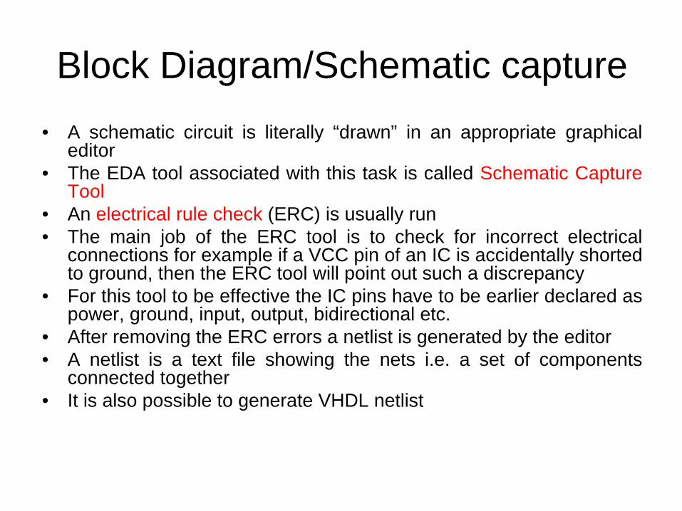
Block Diagram/Schematic capture•
A schematic circuit is literally “drawn”
in an appropriate graphical editor
•
The EDA tool associated with this task is called Schematic Capture Tool
•
An electrical rule check
(ERC) is usually run•
The main job of the ERC tool is to check for incorrect electrical connections for example if a VCC pin of an IC is accidentally shorted to ground, then the ERC tool will point out such a discrepancy
•
For this tool to be effective the IC pins have to be earlier declared as power, ground, input, output, bidirectional etc.
•
After removing the ERC errors a netlist is generated by the editor•
A netlist is a text file showing the nets i.e. a set of components connected together
•
It is also possible to generate VHDL netlist

Block Diagram/Schematic capture

State Diagram entry
•
Many designs are most effectively described /designed by state diagram approach.
•
Effective for sequential designs •
The EDA tools provide a graphical interface so that the designer can directly make an entry of the state diagram and generate the netlist.
•
This method is preferred since it is a fast way of creating the design

State Diagram entry

HDL code entry •
A designer can enter his /her design using a hardware description language (HDL)
•
The HDLs prominent in the industry are “VHDL”
and “Verilog”•
There is another language that is recently making ground called as “System C”
•
Being similar to C language gives it an advantage to be more user friendly and comfortable to designers familiar with C
•
Using the code entry method is the most preferred one since it offers:–
Design flexibility–
Code re-use–
Easy modification–
Tighter control over resources•
A netlist is again created by compiling the HDL code

HDL code entry

Compilation•
At this stage the design is said to be at the Register Transfer Level (RTL)
•
All the data manipulation is done here at the register of the host CPU or we can say that the design is not in terms of the logic gates but “internal”
to the environment
•
After successful compilation of the design using any one of the three methods a netlist is generated which is called the gate-level netlist
•
The design now is translated in terms of the logic gates and modular entities like multiplexers, decoders. Thus we now have the design at Gate-level

Functional Simulation/Verification
•
There are two very different tasks in digital system development–
Verification is the process of determining whether a design meets the specification and performance goals
–
It concerns the correctness of the initial design as well as the refinement processes
–
Testing is the process of detecting the physical defects of a die or a package that occurred during manufacturing

Functional Simulation/Verification
•
A functional test is done by simulating the gate-level design using logic simulators that may be available as a built-in feature of the EDA tool. There are two ways of functional verification:–
Interactive mode•
In the interactive mode the designer can change the input signals and observe the corresponding output behaviour of the design. This method is becomes cumbersome for designs involving large number of inputs and outputs.
–
Batch mode •
Batch mode uses the concept of test-benches (also a piece of VHDL code) that generates test patterns and checks the validity of the output. This mode is attractive for larger designs.
•
If any undesirable behaviour is observed, the designer can correct the flaw by going back to the design entry level
•
It is important here to note that none of the timing aspects have been considered during this simulation. Functional verification can thus be compared to the algorithm testing in conventional programming languages

Synthesis•
Synthesis means to properly put together so as to make the whole complex design
•
At this stage it is necessary to specify the target device, since the synthesis tool (again dedicated software) requires knowing the resources available with the target device
•
Synthesis optimally maps the design functionality (at the gate-level) in to the actual devices available with the target device
•
For example if the design uses a four-
input AND gate but since this is not available with the target device, the synthesis tool can break down the four-
input AND gate
into two two-input AND gates and map correspondingly•
Optimization is very important otherwise the design may get “blown-up”
and the target device may prove too small
for the design•
Synthesis tools have built-in proprietary algorithms for optimization

Post-synthesis simulation•
After synthesis the design needs to be re-
checked to confirm its functionality•
Simulation at this level ensures that the mapped design behaves correctly as desired
•
A possibility may exist wherein, the synthesis tool may incorrectly recompose the design while mapping
•
Again timing parameters are ignored here

Implementation•
This is the process of physical placing of the design into the target device.
•
Though it is a physical placement, it still takes place in the virtual environment provided by the EDA tool
•
A physical map of the target device is loaded into the environment and the components are virtually fitted into the target device.
•
Again this process may have two phases:–
Physical synthesis•
Physical synthesis means optimal relocation of the design into the target device. Proprietary software tools are available for this
task and may be quite costly. This phase is however optional.
–
Place and route•
Place and route is the phase where the tool completes the task of virtually placing the components of the design in to the target device and then wiring the individual modules to complete the design.

Timing Simulation•
One most important change the design undergoes is after the implementation.
•
The modules in the design now may be physically placed apart from each other.
•
This factor introduces the delay aspect in the signal propagation.
•
Many synchronous circuits will fail if the timing aspects are ignored, even though they appear to be functionally perfect!
•
Hence a simulation is necessary again to test the timing behaviour of the design.
•
This provides the designer with a better view of the design functionality.
•
In fact the real-world behaviour of the device can be very accurately studied by the simulation with timing aspects

Hardware Implementation•
The final step in design is to “download”
the functionality into the actual hardware i.e. the target device
•
The synthesis tool generates the output in terms of “bit-stream”
that is used to
configure the target device •
Vendor specific tools can be used for downloading the bit-stream into the physical device
HDL•
A hardware description language (HDL) is a software coding language used to model the intended operation of a piece of hardware
•
There are two aspects to the description of hardware that an HDL
facilitates:–
true abstract behaviour
modeling–
hardware structure modeling•
Abstract behaviour modeling–
A hardware description language is declarative in order to facilitate the abstract description of hardware behaviour
for specification purpose. This behaviour
is not influenced by structural or design aspects of the hardware intent.
•
Hardware structure modeling–
Hardware structure is capable of being modeled in a hardware description language irrespective of the design’s behaviour.

VHDL
•
What is VHDL?–
Digital system design using Hardware Description Language is an established methodology in EDA
–
VHDL stands for “VERY HIGH SPEED INTEGRATED CIRCUITS
HARDWARE DESCRIPTION LANUAGE”
EDA stands for “ELECTRONIC DESIGN AUTOMATION”

FEATURES
•
VHDL is an amalgamation of following languages–
Concurrent language
–
Sequential Language–
Timing Specification
–
Simulation Language–
Test Language

•
VHDL has got powerful language constructs–
{if…else}, {with…select} etc
•
Design hierarchies to create modular designs
•
Supports Design Libraries•
Facilitates device independent design and portability

Concurrent Language
•
Concurrent statements execute at the same time in parallel as in hardware
Z <= C + X ;X <= A + B ;
+
+
A
B
C
X
Z

Sequential Language•
Sequential statements execute one at a time in sequence
•
As the case with any conventional programming language the sequence of statements is important
Z <= C + X ;
X <= A + B;
X <= A + B;
Z <= C + X ; ≠Sequential statements are required to design sequential circuits

Timing Specification
•
Providing timing attributes in a sequential digital design is of prime importance since the operations are synchronized to a common clock
•
Example:processbegin
clk <= ‘0’ ;wait for 20 ns ;clk <= ‘1’ ;wait for 12 ns ;
end process ;
0 20 32 52 64 ns84
Timing can be specified in a process only

Simulation language
•
For analyzing a digital design it is important the design be simulated
•
Simulation has different flavours–
Functional simulation
–
Post-synthesis simulation–
Post-
layout simulation
•
Any HDL should thus be equipped with simulation capability for verification and troubleshooting purposes

Test Language
•
Testbench–
It is a part of a VHDL module that generates a set of test vectors (test inputs) and sends them to the module being tested
–
It collects the responses generated by the module under test and compares them against a specification of correct results
–
Thus testbench
is required to ensure that the design is correct and that the module is operating as desired
Equivalent to checking of logical errors in any conventional programming language

Testbench
use
Testtst_atst_btst_c
MODULE UNDER TEST
ABC.vhdABC_testbench.vhd
Equivalent to mechanical test jigs used for testing functionality of mass produced pcbs as in TV sets or motherboards

Design Hierarchy•
Hierarchy can be represented using VHDL
•
Example–
A full adder which is the top level module being composed of three lower level modules that are; half adder and OR gate
HALFADDER
HALFADDER
OR
AB
Cin
SUM
CARRY
Design hierarchy simplifies the design procedure and manageability in case of complex designs

Design Libraries•
Design Unit–
It is any block of VHDL code or collection of VHDL codes that may be independently analyzed and inserted into a design library
•
Design Library–
It is a storage facility in which analysed
VHDL
descriptions are stored for repeated uses
1
3
2
54
DesignLibrary
Simulator
Analyze
DESIGN UNIT

Logic systems•
Need for multi-valued logic system–
Conventional logic systems have only three values i.e. ‘0’, ‘1’, ‘Z’
•
Example–
Consider the truth-table for AND gate
A B Y0 0 00 1 01 0 01 1 10 Z ?
HOW TO RESOLVE THIS CONDITION ?

•
For this problem a 9-valued logic system or package was developed that is called “STD_LOGIC_1164”
and it is accepted as
IEEE STD 1164-1993•
Multi-valued logic–
Unknown: value was known but not anymore
–
Un-initialized: value was never known–
High impedance: net has no driver
–
Drive strengths: handle different output drivers
–
Don’t care: value is immaterial

Levels of abstraction
•
Different styles are adopted for writing VHDL code
•
Abstraction defines how much detail about the design is specified in a particular description
•
Four levels are:–
Layout level
–
Logic level–
Register Transfer level
–
Behavioral level LOGIC
LAYOUT
RTL
BEHAVIORAL

Layout Level
•
This is the lowest level and describes the CMOS layout level design on silicon

Logic Level
•
Design has information about–
Function
–
Architecture–
Technology
–
Detailed timings•
Layout information and analog effects are ignored

Register Transfer Level
•
Using HDL every register in the design and the logic in between is defined
•
Design contains:–
Architecture information
–
No details of technology–
No specification of absolute timing delays
Behavioral Level
•
Describing function of a design using HDL without specifying the architecture of registers
•
Contains timing information required to represent a function

Basic building blocks of VHDL code
•
A VHDL design is composed of following blocks:–
Library declarations
–
Entity–
Architecture
–
Configuration

Basic VHDL code
LIBRARY DECLARATIONS
ENTITY
ARCHITECTURE
CONFIGURATION
BASIC VHDL CODE

Detailed anatomy of VHDL code
Functions
Procedures
Types
Constants
Components
Package
Library
EntityGenerics Ports
Architecture(Style I)
DATAFLOW
Architecture(Style II)
BEHAVIOURAL
Architecture(Style III)
STRUCTURAL
ConcurrentStatements
ConcurrentStatements
Process
SequentialStatements

Elements of VHDL
R.B.Ghongade
Lecture 3

Basic building blocks
LIBRARYDECLARATIONS
ENTITY
ARCHITECTURE
CONFIGURATION
BASIC VHDL CODE

Overview

Library
• It is a collection of compiled VHDL units• It enables sharing of compiled designs and
hides the source code from the users• Commonly used functions, procedures and
user data types can be compiled into a user defined library for use with all designs
• Library should be declared before each entity declaration even if it is in the same VHDL file

Library• To declare a library (i.e. to make it visible to the
design) two lines of code are needed , onecontaining name of the library, the other a useclause
• A library structure can be as follows:
FUNCTIONSPROCEDURES
TYPESCONSTANTS
COMPONENTS
LIBRARY
PACKAGE

Library syntaxLIBRARY library_name ;USE library_name.package_name.package_parts ;
LIBRARY IEEE ; -- semicolon indicatesUSE IEEE.std_logic_1164.all ; -- end of statement or
-- declarationLIBRARY work ; -- double dash (--)
-- indicates a commentUSE work.all ;
Example

Library detailsIEEE.MATH_COMPLEX.all This package defines a standard for designers
to use in describing VHDL models that make use of common COMPLEX constants and common COMPLEX mathematical functions andoperators.
IEEE.MATH_REAL.all This package defines a standard for designersto use in describing VHDL models that makeuse of common REAL constants and commonREAL elementary mathematical functions.
IEEE.NUMERIC_BIT.all This package defines numeric types andarithmetic functions for use with synthesis tools.Two numeric types are defined:-- UNSIGNED: represents an UNSIGNED number in vector form-- SIGNED: represents a SIGNED number in vector formThe base element type is type BIT.
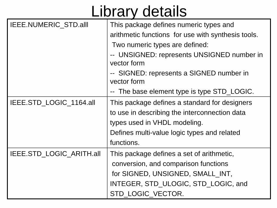
Library detailsIEEE.NUMERIC_STD.alll This package defines numeric types and
arithmetic functions for use with synthesis tools.Two numeric types are defined:-- UNSIGNED: represents UNSIGNED number in vector form-- SIGNED: represents a SIGNED number in vector form-- The base element type is type STD_LOGIC.
IEEE.STD_LOGIC_1164.all This package defines a standard for designers to use in describing the interconnection datatypes used in VHDL modeling.Defines multi-value logic types and related functions.
IEEE.STD_LOGIC_ARITH.all This package defines a set of arithmetic,conversion, and comparison functionsfor SIGNED, UNSIGNED, SMALL_INT, INTEGER, STD_ULOGIC, STD_LOGIC, and STD_LOGIC_VECTOR.

Library detailsIEEE.STD_LOGIC_MISC.alll This package defines supplemental types,
subtypes, constants, and functions for the Std_logic_1164 Package.
IEEE.STD_LOGIC_SIGNED.all This package defines a set of signedarithmetic, conversion, and comparison functions for STD_LOGIC_VECTOR.
IEEE.STD_LOGIC_TEXTIO.all This package overloads the standard TEXTIO procedures READ and WRITE.
IEEE.STD_LOGIC_UNSIGNED.all This package defines a set of unsigned arithmetic, conversion and comparison functions for STD_LOGIC_VECTOR.

Entity
– It is the design’s interface to the external circuitry
– Equivalent to pinout /package of an IC– VHDL design must include one and only one
entity per module– It can be used as a component in other
entities after being compiled into a library

Entity declaration• Defines the input and output ports of the design• Name of the entity can be anything other than
the reserved VHDL word• Each port in the port list must be allotted:
– a name ( should be self-explanatory that provides information about its function
– data flow direction or mode– a type
• Ports should be well documented with comments at the end of line providing additional information about the signal

Entity syntax
entity entity_name isport ( port_name : signal_mode signal_type ;
port_name : signal_mode signal_type ;port_name : signal_mode signal_type ) ;
end entity_name ;

Modes
• Ports in the portlist have modes which indicate the driver direction
• Mode also indicates whether or not the port can be read from within the entity
• Four modes are available:– Mode IN– Mode OUT– Mode INOUT– Mode BUFFER

• Mode INValue can be read from but not assigned to (by the entity)
ENTITY
Port signal A
Drivers resideoutside the entity
port ( A : in std_logic ) ;

• Mode OUTValue can be assigned to but not read from (by the entity)
port ( B : out std_logic ) ;
ENTITY
Port signal B
Drivers resideinside the entity
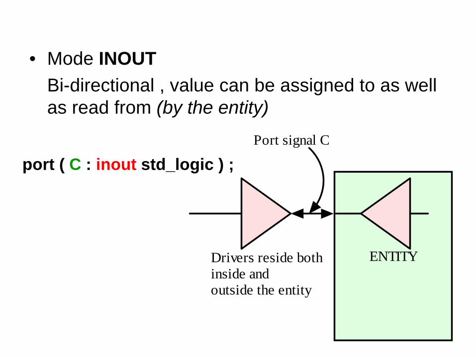
• Mode INOUTBi-directional , value can be assigned to as well as read from (by the entity)
port ( C : inout std_logic ) ;
ENTITY
Port signal C
Drivers reside bothinside andoutside the entity

• Mode BUFFEROutput port with internal read capability
port ( D : buffer std_logic ) ;
ENTITY
Port signal D
Drivers resideinside the entity
Signal can be read inside the entityDO NOT USE UNLESS REQUIRED

Entity exampleentity and_gate is
port ( 1A , 2A , 3A, 4A : in std_logic ; 1B , 2B , 3B, 4B : in std_logic ; 1Y , 2Y , 3Y, 4Y : out std_logic ) ;
end and_gate ;
1A1
1B2
1Y3
2A4
2B5
2Y6
GND7 3Y 8
3A 9
3B 10
4Y 11
4A 12
4B 13
VCC 14

Entity exampleentity ALU is
port ( In1 : in std_logic_vector ( 3 downto 0) ; -- 1st operandIn2 ; in std_logic_vector ( 3 downto 0) ; -- 2nd operandOpsel : in std_logic_vector ( 3 downto 0) ; -- opn selectCin : in std_logic ;Mode : in std_logic ;Result : out std_logic_vector ( 3 downto 0 ) ;Cout : out std_logic ;Equal : out std_logic ) ;
end ALU ;
ALU
In1 In2 Opsel
Result
Cout
Mode
Cin
Equal

ArchitectureIt specifies
• Behaviour• Function• Relationship between inputs and outputs of an entity
Syntaxarchitecture achitecture_name of entity_name is
[declarations] -- optionalbegin
code -- concurrent statements onlyend achitecture_name ;

• Architecture can contain only concurrent statements
• A design can be described in an architecture using various levels of abstraction
• An entity can have more than one architectures since a function can be implemented in a number of ways
• There can be no architecture without an entity
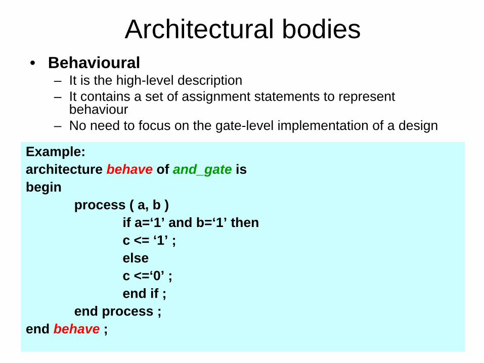
Architectural bodies• Behavioural
– It is the high-level description– It contains a set of assignment statements to represent
behaviour– No need to focus on the gate-level implementation of a design
Example:architecture behave of and_gate isbegin
process ( a, b )if a=‘1’ and b=‘1’ thenc <= ‘1’ ;elsec <=‘0’ ;end if ;
end process ;end behave ;

• Dataflow– It uses concurrent signal assignment
statements
Example:architecture dataflow of and_gate isbegin
c<= a and b ;end dataflow ;

• Structural– Components from libraries are connected
together– Designs are hierarchical– each component can be individually simulated– it makes use of component instantiation
HALFADDER
HALFADDER
OR
AB
Cin
SUM
CARRY
Functional unitsTop level design

Configuration• Since a number of architectures can exist
for an entity , using configuration statement we can bind a particular architecture to the entity
configuration CONFIGURATION_NAME of ENTITY_NAME isfor ARCHITECTURE_NAMEend for;
end CONFIGURATION_NAME;
Syntax

Language elements
Next class

Language Elements I
R.B.GhongadeLecture 4

• VHDL is a strongly typed language– Designers have to declare the type before
using it• VHDL is not case sensitive ( but avoid
mixed cases as a good programming practice)
• VHDL supports a wide variety of data types and operators– OBJECTS– OPERATORS– AGGREGATES

Objects• They are used to represent and store the
data in the design being described• Object contains a value of specific type
Class Object Data type
SIGNAL COUNT : INTEGER
This results in an object called COUNT that holds INTEGER value that belongs to class SIGNAL
• The name given to the object is called as identifier
• Do not use reserved words as identifiers

• Each object has a data type and class• Class indicates how the object is used in the
module and what can be done with that object• Type indicates what type of data the object
contains• Each object belongs to one of the following class:
– CONSTANT– SIGNAL– VARIABLE– FILES
CONSTANT SIGNAL VARIABLE
CLASS
FILES
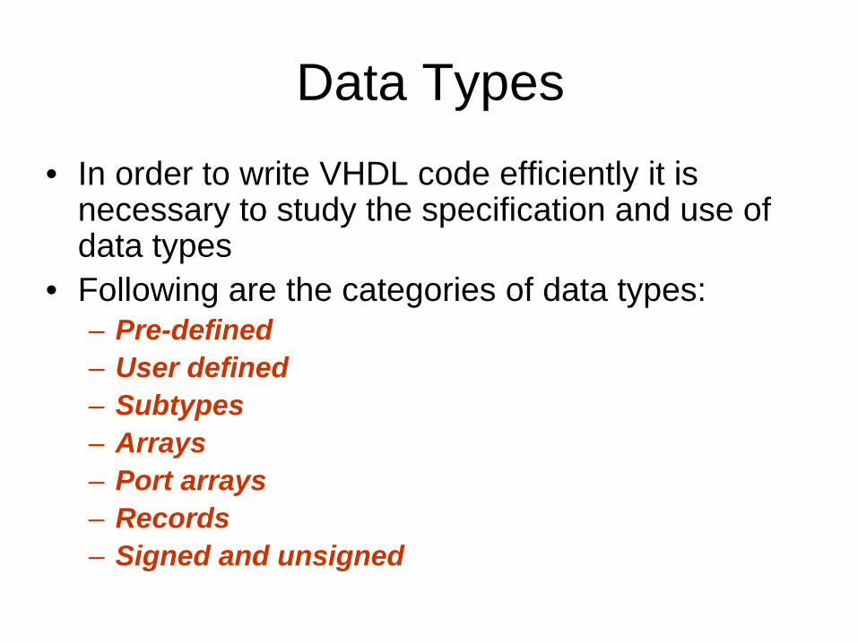
Data Types• In order to write VHDL code efficiently it is
necessary to study the specification and use of data types
• Following are the categories of data types:– Pre-defined– User defined– Subtypes– Arrays– Port arrays– Records– Signed and unsigned

Pre-defined data types• Specified by IEEE 1076 and IEEE 1164
Package Library Type/Functions
standard std BIT, BOOLEAN, INTEGER, REAL
std_logic_1164 ieee STD_LOGIC, STD_ULOGIC
std_logic_arith ieee SIGNED, UNSIGNED / data conversion functions
std_logic_signed ieee Functions that allow operations with STD_LOGIC_VECTOR
std_logic_unsigned ieee

BIT (and BIT_VECTOR): 2 level logic (‘0’, ‘1’)
Examples:
SIGNAL X : BIT ;
X is declared as a one-
digit SIGNAL of type BIT
SIGNAL Y : BIT_VECTOR (3 downto 0);Y is 4-bit vector,
leftmost bit is MSB
SIGNAL W : BIT_VECTOR (0 to 7);W is 8-bit
vector, rightmost bit
is MSB

• To assign a value to the signal use the operator “ < = ”
• Assignment examples:
X <= ‘1’ ; X is a single bit SIGNAL whose value is ‘1’Note that single quotes are used for a single bit
Y <= “0111” ; Y is a 4- bit SIGNAL whose value is “0111” . Note that double quotes are used for vectors
W <= “01110001” ; W is an 8- bit SIGNAL whose value is “0111001” . MSB is ‘1’

STD_LOGIC (and STD_LOGIC_VECTOR): 8 valued logic (introduced in IEEE 1164 standard)
Symbol Description Remark‘X’ Forcing unknown Synthesizable unknown
‘0’ Forcing low Synthesizable logic ‘0’
‘1’ Forcing high Synthesizable logic ‘1’
‘Z’ High impedance Synthesizable tri-state buffer
‘W’ Weak unknown‘L’ Weak low‘H’ Weak high‘-’ Don’t care

Examples:
SIGNAL X : STD_LOGIC ;
X is declared as a one-digit (scalar) SIGNAL of type
STD_LOGIC
SIGNAL Y : STD_LOGIC_VECTOR (3 downto 0);Y is 4-bit
vector, leftmost bit is MSB
SIGNAL Y : STD_LOGIC_VECTOR (3 downto 0) : = “0001”for (optional)
initial value use“ := ”
Most of std_logic levels are intended for simulationonly. However ‘0’, ‘1’ and ‘Z’ are synthesizable withno restrictions

• With respect to “weak” values, they are resolved in favour of the “forcing” values in multiple-driven nodes. If any two std_logic signals are connected to the same node, then conflicting logic levels are resolved by using the shown table
X 0 1 Z W L H -X X X X X X X X X0 X 0 X 0 0 0 0 X1 X X 1 1 1 1 1 XZ X 0 1 Z W L H ZW X 0 1 W W W W XL X 0 1 L W L W XH X 0 1 H W W H X- X X X X X X X X
•The STD_ULOGIC has 9 valued logic levels : additional value is ‘U’ for “Un-resolved or ”Un-initialized”
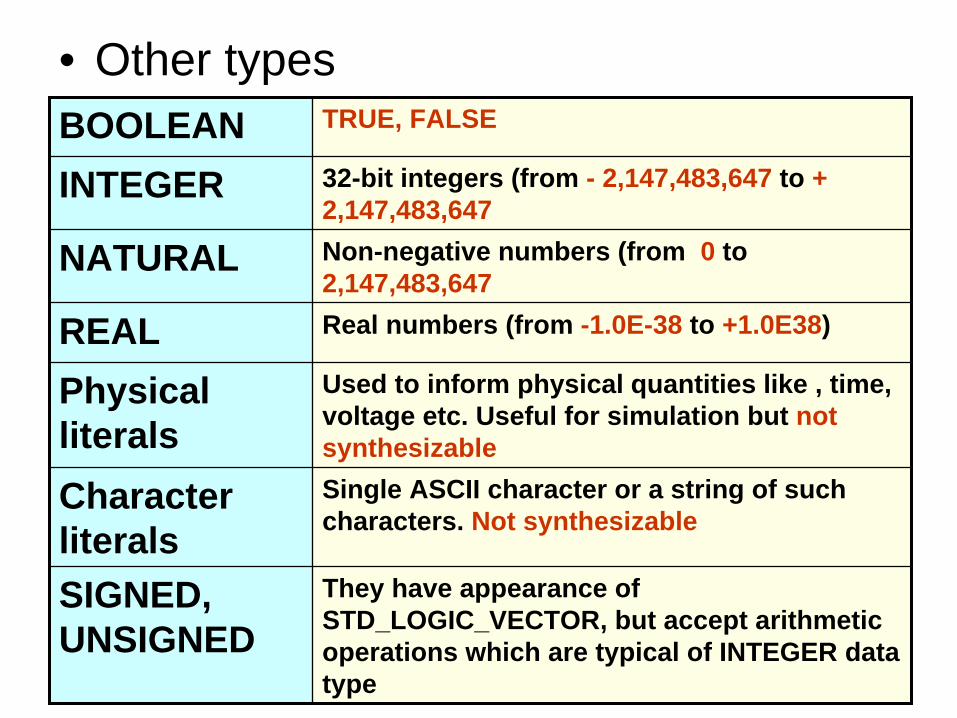
• Other typesBOOLEAN TRUE, FALSE
INTEGER 32-bit integers (from - 2,147,483,647 to + 2,147,483,647
NATURAL Non-negative numbers (from 0 to 2,147,483,647
REAL Real numbers (from -1.0E-38 to +1.0E38)
Physical literals
Used to inform physical quantities like , time, voltage etc. Useful for simulation but not synthesizable
Character literals
Single ASCII character or a string of such characters. Not synthesizable
SIGNED, UNSIGNED
They have appearance of STD_LOGIC_VECTOR, but accept arithmetic operations which are typical of INTEGER data type

User defined data types
• VHDL allows user defined data types• Two categories of this data type are:
– Integer– Enumerated
• User defined integer typeTYPE my_integer IS RANGE -32 to +32 ;
TYPE student_grade IS RANGE 0 to 100 ;

• User defined enumerated typeTYPE my_logic IS (‘0’, ‘1’, ‘Z’ );
TYPE my_state IS ( idle, forward, backward, stop) ;
An enumerated type, typically used in state machines
• The encoding of enumerated types is done sequentially and automatically
• Since here there are 4 states only two bits are required hence “00” is assigned to first state ( idle), “01” to second state (forward) and so on.

Subtypes
• A SUBTYPE is a TYPE with a constraint• Though operations between data of
different types are not allowed, they are allowed between the subtype and its corresponding base type
SUBTYPE sub_state IS my_state RANGE idle to backward ;
This means that the subtype sub_state =(idle, forward, backward)

Arrays• Arrays are collections of objects of same type• Can be 1-dimensional, 2-dimensional or
1D X 1D• Higher dimensional arrays are possible but not
synthesizable
0 0 1 0 0
1 0 1 0
1 1 0 0
0 1 0 0
1 1 0 1
0 1 0 1 0
1 0 1 1 0
0 1 0 1 0Scalar 1D
1D x 1D2D data array

Array syntax
TYPE type_name IS ARRAY (specification) OF data_type ;
To specify an array :
SIGNAL signal_name : type_name [:= initial_value]
To use an array :

Example : 1D x 1D array– We want to build an array containing 4
vectors, each of size 8 bits– we will call each vector as row and the
complete array as matrix
TYPE row IS ARRAY (7 downto 0 ) OF STD_LOGIC ;TYPE matrix IS ARRAY (3 downto 0 ) OF row ;SIGNAL X : matrix ;
1D x 1D SIGNAL

Example : 2D array– This array will be created with scalars only
TYPE matrix2D IS ARRAY (0 TO 3, 7 DOWNTO 0 ) OF STD_LOGIC ;
L
M L
M
ROWS
COLUMNS
Port Arrays
• In the specification of the input or output pins (PORTS) of a circuit (which is made in the ENTITY), we might need to specify the ports as arrays of vectors.
• Since TYPE declarations are not allowed in an ENTITY, the solution is to declare user-defined data types in a PACKAGE, which will then be visible to the whole design (thus including the ENTITY)

-------
Package: --------------------------LIBRARY
ieee;USE ieee.std_logic_1164.all;----------------------------PACKAGE my_data_types
ISTYPE vector_array
IS ARRAY (NATURAL RANGE <>) OFSTD_LOGIC_VECTOR(7
DOWNTO 0);END my_data_types;---------------------------------------------------
Main code: -------------------------LIBRARY ieee;USE
ieee.std_logic_1164.all;USE work.my_data_types.all; --
user-defined package---------------------------ENTITY mux
ISPORT (inp: IN VECTOR_ARRAY (0
TO 3);... );END mux;... ;--------------------------------------------

• As can be seen in the example above, a user- defined data type, called vector_array,was created, which can contain an indefinite number of vectors of size eight bits each (NATURAL RANGE <> signifies that the range is not fixed, with the only restriction that it must fall within the NATURAL range, which goes from 0 to +2,147,483,647)
• The data type was saved in a PACKAGE called my_data_types, and later used in an ENTITY to specify a PORT called inp
• Notice in the main code the inclusion of an additional USE clause to make the user-defined package my_data_types visible to the design.

Records
• Records are similar to arrays, with the only difference that they contain objects of different types.
TYPE birthday IS RECORDday: INTEGER RANGE 1 TO 31;month: month_name;END RECORD;

Signed and Unsigned data types
• These types are defined in the std_logic_arith package of the ieee library
Examples:SIGNAL x: SIGNED (7 DOWNTO 0);SIGNAL y: UNSIGNED (0 TO 3);

• An UNSIGNED value is a number never lower than zero. For example, ‘‘0101’’represents the decimal 5, while ‘‘1101’’ signifies 13.
• If type SIGNED is used instead, the value can be positive or negative (in two’s complement format). Therefore,‘‘0101’’ would represent the decimal 5, while ‘‘1101’’ would mean 3.
• To use SIGNED or UNSIGNED data types, the std_logic_arith package, of the ieee library, must be declared

Next class
Language Elements II

Language Elements II
R.B.GhongadeLecture 5

Operators
• VHDL provides several kinds of pre- defined operators– Assignment operators– Logical operators– Arithmetic operators– Relational operators– Shift operators– Concatenation operators

Assignment operators• Are used to assign values to signals, variables,
and constants.
<= Used to assign a value to a SIGNAL
:=
Used to assign a value to a VARIABLE, CONSTANT, orGENERICUsed also for establishing initial values
=> Used to assign values to individual vector elements or with OTHERS

SIGNAL x : STD_LOGIC;VARIABLE y : STD_LOGIC_VECTOR(3 DOWNTO 0); SIGNAL w: STD_LOGIC_VECTOR(0 TO 7);
x <= '1'; -- '1' is assigned to SIGNAL x using "<="y := "0000"; -- "0000" is assigned to VARIABLE y using
--":="w <= "10000000"; -- LSB is '1', the others are '0'w <= (0 =>'1', OTHERS =>'0'); -- LSB is '1', the others
-- are '0'
Then the following assignments are legal:

Logical operators
• Used to perform logical operations. • The data must be of type:
– BIT, STD_LOGIC – STD_ULOGIC – BIT_VECTOR– STD_LOGIC_VECTOR– STD_ULOGIC_VECTOR

• The logical operators are:– NOT– AND– OR– NAND– NOR– XOR– XNOR
The NOT operator has precedence
over the others
Examples:y <= NOT a AND b; -- (a'.b)y <= NOT (a AND b); -- (a.b)'y <= a NAND b; -- (a.b)'
Arithmetic operators
• Used to perform arithmetic operations. The data can be of type INTEGER, SIGNED, UNSIGNED, or REAL (the last cannot be synthesized directly).
• Also, if the std_logic_signed or the std_logic_unsigned package of the ieee library is used, then STD_LOGIC_VECTOR can also be employed directly in addition and subtraction operations

+ ( Addition)- (Subtraction)* (Multiplication)/ (Division)** (Exponentiation)MOD ( Modulus)REM ( Remainder)ABS ( Absolute value)
•There are no synthesis restrictions regarding addition and subtraction, and the same is generally true for multiplication
•For division, only power of two dividers (shift operation) are allowed
•For exponentiation, only static values of base and exponentare accepted •Regarding the mod and rem operators, y mod x returns the remainder of y/x with the signal of x, while y rem x returns the remainder of y/x with the signal of y
•Finally, abs returns the absolute value
For mod, rem, abs , there generally is little or no synthesis support

Comparison operators
= Equal to/= Not equal to< Less than> Greater than<= Less than or equal to>= Greater than or equal to
Also called RELATIONAL operators

Shift operatorssll shift left logicalsrl shift right logicalsla shift left arithmeticsra shift right arithmeticror rotate left logicalrol rotate right logical
0
0
LOGICAL SHIFTING
ARITHMETIC SHIFTING(retains sign bit)
ROTATE
• LOGICAL• ARITHMETIC• ROTATE

Concatenation operator
• Operands can be one-dimensional array type or element type
• “ &” works on vectors only
& Concatenation
Example:SIGNAL a : STD_LOGIC_VECTOR ( 5 DOWNTO 0 ) ;SIGNAL b,c,d : STD_LOGIC_VECTOR ( 2 DOWNTO 0 ) ;BEGIN
b <= ‘0’ & c(1) & d(2) ;a <= c & d ;
. . .

Operator summary
Operator type Operators Data types
Logical NOT, AND, ANDOR, NOR, XOR,
XNOR
BIT, BIT_VECTOR, STD_LOGIC, STD_LOGIC_VECTOR, STD_ULOGIC, STD_ULOGIC_VECTOR
Arithmetic +, -,*,/,** (mod, rem , abs) INTEGER, SIGNED, UNSIGNED
Comparison =, /=, <, >, <=, >= All above
Shift sll, srl, sla, sra, rol, ror BIT_VECTOR
Concatenation &, ( , , , ) Same as for logical operators, plusSIGNED and UNSIGNED

Operator overloading
• Operators can be user-defined• Let us consider the pre-defined arithmetic
operators seen earlier (+,- , *, /, etc.). They specify arithmetic operations between data of certain types (INTEGER, for example)
• For instance, the pre-defined ‘‘+’’ operator does not allow addition between data of type BIT.
• We can define our own operators, using the same name as the pre-defined ones

• For example, we could use ‘‘+’’ to indicate a new kind of addition, this time between values of type BIT_VECTOR. This technique is called operator overloading
• Example: Consider that we want to add an integer to a binary 1-bit number. Then the following FUNCTION could be used
FUNCTION "+" (a: INTEGER, b: BIT) RETURN INTEGER ISBEGINIF (b='1') THEN RETURN a+1;ELSE RETURN a;END IF;END "+";

A call to the function above could thus be the following:SIGNAL inp1, outp: INTEGER RANGE 0 TO15;
SIGNAL inp2: BIT;(...)outp <= 3 + inp1 + inp2;(...)
• In ‘‘outp<=3+inp1+inp2;’’, the first ‘‘+’’ is the pre- defined addition operator (adds two integers), while the second is the overloaded user-defined addition operator (adds an integer and a bit).

Aggregates
• It assigns values to elements of an array
a <= (OTHERS => ‘0’ ) ; a <= “0000” ;
• We can assign values to some bits in a vector and use “OTHERS” clause to assign default values to remaining bits
a <= (0 => ‘1’, 2 => ‘1’, OTHERS => ‘0’ ) ;
is equivalent to a <= “00101” ;
Useful when we are dealing with large vectors

• Each object has a data type and class• Class indicates how the object is used in the
module and what can be done with that object• Type indicates what type of data the object
contains• Each object belongs to one of the following class:
– CONSTANT– SIGNAL– VARIABLE
CONSTANT SIGNAL VARIABLE
CLASS
Classes re-visited
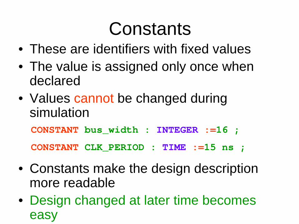
Constants• These are identifiers with fixed values• The value is assigned only once when
declared• Values cannot be changed during
simulationCONSTANT bus_width : INTEGER :=16 ;
CONSTANT CLK_PERIOD : TIME :=15 ns ;
• Constants make the design description more readable
• Design changed at later time becomes easy

Signals
Equivalent to wireswithin a circuit
Example:architecture and_gate of myand issignal TEMP : STD_LOGIC ;begin
U1 : AND2 portmap ( a, b, TEMP ) ;U2 : AND2 portmap (TEMP, c , d ) ;
end and_gate ;
a
bAND2
TEMP
cAND2
d

• Thus signals are used :– to connect design entities together and
communicate changes in values within a design
– instead of INOUT mode• Each signal has a history of values i.e.
they hold a list of values which include current value of the signal and a set of possible future values that can appear on the signal
• Computed value is assigned to signal after specified delay called DELTA DELAY

Variables
• These are objects with single current value
• They are used to store the intermediate values between the sequential statements
• Variable assignment occurs immediately• Variables can be declared and used inside
the process statement only. But they retain their value throughout the entire simulation

process ( a )variable count : INTEGER : = 1 ;begin
count : = count+ 1 ;end process ;
Example :
count contains the total number of events that occurred on signal a

Language elements III
Next class

Language Elements III
R.B.GhongadeLecture 6

Attributes
• An attribute is data that are attached to VHDL objects or predefined data about VHDL objects
• Examples are the current drive capability of a buffer or the maximum operating temperature of the device
• Types are– Data Attributes– Signal Attributes– User-defined Attributes

Data AttributesThe pre-defined, synthesizable data attributes
are the following:• d’LOW : Returns lower array index• d’HIGH : Returns upper array index• d’LEFT : Returns leftmost array index• d’RIGHT : Returns rightmost array index• d’LENGTH : Returns vector size• d’RANGE : Returns vector range• d’REVERSE_RANGE: Returns vector range
in reverse order

Example
Consider the following signal:SIGNAL d : STD_LOGIC_VECTOR (7 DOWNTO 0);
Then:d'LOW=0, d'HIGH=7, d'LEFT=7, d'RIGHT=0, d'LENGTH=8, d'RANGE=(7 downto 0), d'REVERSE_RANGE=(0 to 7)

If the signal is of enumerated type, then:• d’VAL(pos) : Returns value in the position
specified• d’POS(value) : Returns position of the
value specified• d’LEFTOF(value) : Returns value in the
position to the left of the value specified• d’VAL(row, column) : Returns value in the
position specified; etcThere is little or no synthesis support for enumerated data type attributes

Signal AttributesLet us consider a signal sThen:• s’EVENT : Returns true when an event occurs
on s• s’STABLE : Returns true if no event has
occurred on s• s’ACTIVE : Returns true if s = ‘1’• s’QUIET <time> : Returns true if no event has
occurred during the time specified• s’LAST_EVENT : Returns the time elapsed since last
event• s’LAST_ACTIVE: Returns the time elapsed since
last s=‘1’• s’LAST_VALUE : Returns the value of s before the
last event; etc.

ExampleAll four assignments shown below are synthesizable and equivalent. They return TRUE when an event (a change) occurs on clk, AND if such event is upward(in other words, when a rising edge occurs on clk)
IF (clk'EVENT AND clk='1')... -- EVENT attribute-- used with IF
IF (NOT clk'STABLE AND clk='1')... -- STABLE --attribute used-- with IF
WAIT UNTIL (clk'EVENT AND clk='1'); -- EVENT --attribute used-- with WAIT
IF RISING_EDGE(clk)... -- call to a function

User-defined Attributes• VHDL also allows the construction of user-defined
attributes• To employ a user-defined attribute, it must be
declared and specifiedAttribute Declaration:
ATTRIBUTE attribute_name: attribute_type ;
Attribute Specification:
ATTRIBUTE attribute_name OF target_name: class IS value;
where:attribute_type: any data type (BIT, INTEGER, STD_LOGIC_VECTOR, etc.)class: TYPE, SIGNAL, FUNCTION, etc.value: ‘0’, 27, ‘‘00 11 10 01’’, etc.

ExampleATTRIBUTE number_of_inputs: INTEGER;
ATTRIBUTE number_of_inputs OF nand3: SIGNAL IS 3;
...
inputs <= nand3'number_of_inputs; -- attribute call, -- returns 3

Generics• As the name suggests, GENERIC is a way
of specifying a generic parameter• a static parameter that can be easily
modified and adapted to different applications
• The purpose is to make the code more flexible and reusable
• must be declared in the ENTITY• More than one GENERIC parameter can
be specified in an ENTITY

SyntaxGENERIC (parameter_name : parameter_type := parameter_value);
The GENERIC statement below specifies a parameter called n, of type INTEGER, whose default value is 8. Therefore, whenever n is found in the ENTITY itself or in the ARCHITECTURE (one or more) that follows, its value will be assumed to be 8
ENTITY my_entity ISGENERIC (n : INTEGER := 8; vector: BIT_VECTOR := "00001111");PORT (...);END my_entity;ARCHITECTURE my_architecture OF my_entity IS...END my_architecture;
Example
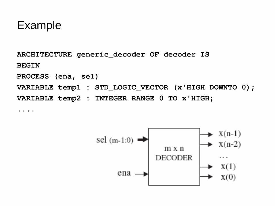
ARCHITECTURE generic_decoder OF decoder ISBEGINPROCESS (ena, sel)VARIABLE temp1 : STD_LOGIC_VECTOR (x'HIGH DOWNTO 0);VARIABLE temp2 : INTEGER RANGE 0 TO x'HIGH;....
Example

Delays in VHDL
• In VHDL, there are three types of delay that are encountered
– Inertial delay– Transport delay– Delta delay

Inertial Delay
• Inertial delay is the default in VHDL• Behaves similarly to the actual device• Output signal of the device has inertia,
which must be overcome for the signal to change value
• The inertial delay model is by far the most commonly used in all currently available simulators

Inertial delay prevents prolific propagation of spikes throughout the circuit
LIBRARY IEEE;USE IEEE.std_logic_1164.ALL;ENTITY buf ISPORT ( a : IN std_logic;PORT ( b : OUT std_logic);END buf;ARCHITECTURE buf OF buf ISBEGINb <= a AFTER 20 ns;END buf;
Due to inertial delay pulse is swallowed up
Transport Delay
• It represents a wire delay in which any pulse, no matter how small, is propagated to the output signal delayed by the delay value specified
• Especially useful for modeling delay line devices, wire delays on a PCB, and path delays on an ASIC

LIBRARY IEEE;USE IEEE.std_logic_1164.ALL;ENTITY delay_line ISPORT ( a : IN std_logic;PORT ( b : OUT std_logic);END delay_line;ARCHITECTURE delay_line OF delay_line ISBEGINb <= TRANSPORT a AFTER 20 ns;END delay_line;
Pulse is simply delayed

Delta delay• These are used since the PC that
processes and simulates a concurrent phenomenon is basically a sequential machine
• The simulation program mimics concurrency by scheduling events in some order
• Simulation deltas are used to order some types of events during a simulation
• Specifically, zero delay events must be ordered to produce consistent results

Circuit that shows the difference!
CLK
D
E
Q'
Q
DFF
CLK
A
B
C
F
D
Zero delay componentsCLK=‘1’A=‘1’
Assumptions

Problem when no delta delay concept is used
CLK
D
E
Q'
Q
DFF
CLK
A
B
C
F
CLK
D
E
Q'
Q
DFF
CLK
A
B
C
F
CLK
D
E
Q'
Q
DFF
CLK
A
B
C
F
1) A becomes 0
2) Evaluate inverter
3) B <= 1
4) Evaluate AND with C=1
5) D<=1
6) Evaluate NAND
7) C<=0CLK
D
E
Q'
Q
DFF
CLK
A
B
C
F
8) Evaluate AND
9) D<=0
CLK
D
E
Q'
Q
DFF
CLK
A
B
C
F
DUnwanted D assertion
DD

Problem when no delta delay concept is used
CLK
D
E
Q'
Q
DFF
CLK
A
B
C
F
DD
1) A becomes 0
2) Evaluate inverter
3) B <= 1
4) Evaluate NAND
5) C<=0
6) Evaluate AND
7) D<=0
CLK
D
E
Q'
Q
DFF
CLK
A
B
C
F
CLK
D
E
Q'
Q
DFF
CLK
A
B
C
F
D
CLK
D
E
Q'
Q
DFF
CLK
A
B
C
F

Delta delay useDelta 1
Delta 2
Delta 3
Delta 4
10 ns
11 ns
A<=0Evaluate inverter
B<=0Evaluate AND
Evaluate NAND
D<= 1C<=0
Evaluate AND
D<= 0
To summarize, simulation deltas are an infinitesimal amount of timeused as a synchronization mechanism when 0 delay events are present.

Concurrent Statements and
Constructs

Combinational vs. Sequential LogicThe output of the circuit depends solely on thecurrent inputs
Output does depend onprevious inputs hence storage elements arerequired
Combinational Logic
outputinput
StorageElements
PresentState
NextState
Combinational Logic outputinput

Concurrent Code• Consider the following
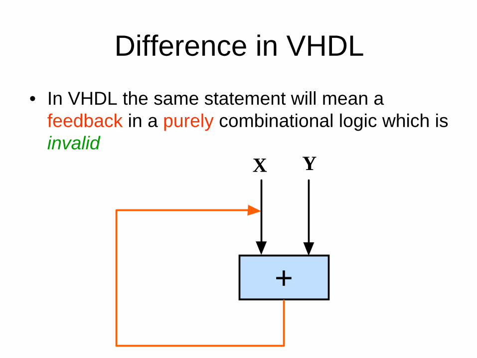
statement:X = X + Y ;
In conventional softwareX and Y are registerlocations hence contentsof X and Y are added andstored in X
Register X Register Y
+
Difference in VHDL
• In VHDL the same statement will mean a feedback in a purely combinational logic which is invalid
+
X Y

• VHDL code is inherently concurrent (parallel)• Only statements placed inside a PROCESS,
FUNCTION, or PROCEDURE are sequential• Concurrent code is also called dataflow code• Order does not matter • We can only build combinational logic circuits
with concurrent code• Concurrent assignment produces one driver for
each assignment statement
z <= a;a z

Multiple driver assignmentarchitecture ABC of XYZ issignal z,a,b,c,d : std_logic ;begin
z <= a and b;z <= c and d;
. . .
?
a
b
c
d
z
Care has to be taken to handle such conditions with a hi-impedance state

Concurrent constructs
Next Class

Concurrent Constructs
R.B.GhongadeLecture 7

Types of concurrent constructs
• when … else• with … select
These constructs need not be in the process

when…else• A concurrent statement which assigns one of
several expressions to a signal, depending on the values of Boolean conditions which are tested in sequence
• Equivalent to a process containing an if statement
Syntax[Label:] Target <= [Options]Expression [after TimeExpression] when Condition else
Expression [after TimeExpression] when Condition else
...Expression [after TimeExpression] [when Condition];

Where to use ?architecture – begin – HERE - endblock – begin – HERE - endgenerate – begin – HERE - end
Rules:• The reserved word guarded may only appear in a
signal assignment within a guarded block. A guarded assignment only executes when the guard expression on the surrounding block is true
• An Expression on the right hand side may be replaced by the reserved word “unaffected”

Synthesis• Conditional signal assignments are synthesized to
combinational logic• The Expressions on the right hand side are multiplexed
onto the Target signal• The resulting logic will be priority encoded, because the
conditions are tested in sequence
Remarks:• Conditional and selected signal assignments are a
concise way to describe combinational logic in Register Transfer Level descriptions, although processes can be easier to read and maintain in some cases
• A conditional assignment is a neat way to convert from a Boolean condition to the type Std_logic

Examplez <= a when s1=‘1’else
b when s2=‘1’else
c ;
c
b
as2
s1
z
MUX21
MUX21

Example (Tri-state Buffer)architecture tri_buff of tri_buff_part isbeginout1 <= in1 when control=‘1’
else‘z’;
end tri_buff ;
in1 out1
control

with…select• A concurrent statement which assigns
one of several expressions to a signal,depending on the value of the expression atthe top.
• Equivalent to a process containing a case statement
Syntax[Label:] with Expression selectTarget <= [Options]Expression [after TimeExpression] when Choices,Expression [after TimeExpression] when Choices,Expression when others;

Where to use ?architecture – begin – HERE – endblock – begin – HERE – endgenerate – begin – HERE – end
Rules:• Every case of the Expression at the top must be
covered once and only once by the choices• An Expression on the right hand side may be
replaced by the reserved word “unaffected”• All possible choices must be enumerated• “others” clause is important since we have 9-
valued logic

Synthesis• Selected signal assignments are
synthesized to combinational logic• The Expressions on the right hand side
are multiplexed onto the Target signal
Remarks:• Conditional and selected signal
assignments are a good way to describecombinational logic in Register Transfer Level descriptions

Example (Multiplexer)architecture mux41 of mux is -- Assumptionsbegin -- a,b,c,d,z arewith control select -- std_logicz <= a when “00” , -- control is
b when “01” ,-- std_logic_vector(1 downto 0)c when “10” ,
d when “11” ,‘Z’ when others ;
end mux41 ;
control
abcd
zMUX41

Block
• There are two types of blocks– Simple– Guarded
Simple block
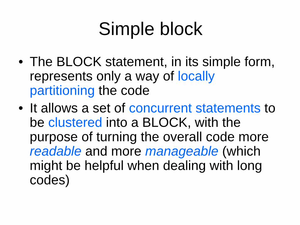
• The BLOCK statement, in its simple form, represents only a way of locally partitioning the code
• It allows a set of concurrent statements to be clustered into a BLOCK, with the purpose of turning the overall code more readable and more manageable (which might be helpful when dealing with long codes)

Syntaxlabel: BLOCK[declarative part]BEGIN(concurrent statements)END BLOCK label;
ARCHITECTURE example ...BEGIN...block1: BLOCKBEGIN...END BLOCK block1 ;...block2: BLOCKBEGIN...END BLOCK block2 ;...END example ;
General form of architecture using
block for partitioning

• Block can be nested inside another blockSyntax
label1: BLOCK[declarative part of top block]BEGIN[concurrent statements of top block]label2: BLOCK[declarative part nested block]BEGIN(concurrent statements of nested block)END BLOCK label2;[more concurrent statements of top block]END BLOCK label1;

Guarded block• A guarded BLOCK is a special kind of
BLOCK, which includes an additional expression, called guard expression
• A guarded statement in a guarded BLOCK is executed only when the guard expression is TRUE
Syntaxlabel: BLOCK (guard expression)[declarative part]BEGIN(concurrent guarded and unguarded statements)END BLOCK label;
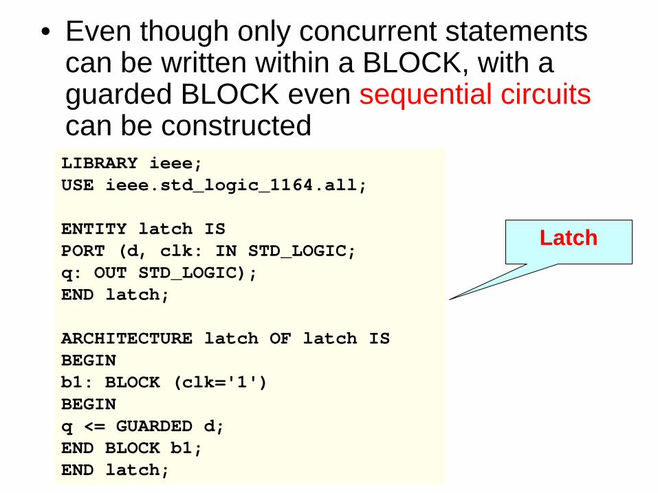
• Even though only concurrent statements can be written within a BLOCK, with a guarded BLOCK even sequential circuits can be constructedLIBRARY ieee;USE ieee.std_logic_1164.all;
ENTITY latch ISPORT (d, clk: IN STD_LOGIC;q: OUT STD_LOGIC);END latch;
ARCHITECTURE latch OF latch ISBEGINb1: BLOCK (clk='1')BEGINq <= GUARDED d;END BLOCK b1;END latch;
Latch

LIBRARY ieee;USE ieee.std_logic_1164.all;
ENTITY DFF ISPORT (d, clk, rst: IN STD_LOGIC;q: OUT STD_LOGIC);END DFF;
ARCHITECTURE DFF OF DFF ISBEGINb1: BLOCK (clk’EVENT AND clk='1')BEGINq <= GUARDED ‘0’ WHEN rst=‘1’ ELSE d;END BLOCK b1;END DFF;
Here, a positive-edge sensitive D-type flip-flop, with synchronous reset, is designed.In it, clk'EVENT AND clk='1' is the guard expression, whileq <= GUARDED '0‘ WHEN rst='1' is a guarded statement. Therefore, q<='0' will occur when the guard expression is true and rst is ‘1’
DFF

Homework Problems
1)Generic encoder
2) 8- bit ALU

For ALU in problem 2sel Operation Function Unit
0000 y <= a Transfer a
Arithmetic
0001 y <= a+1 Increment a 0010 y <= a-1 Decrement a 0011 y <= b Transfer b 0100 y <= b+1 Increment b 0101 y <= b-1 Decrement b 0110 y <= a + b Add a and b 0111 y <= a + b + cin Add a and b with carry 1000 y <= NOT a Complement a
Logic
1001 y <= NOT b Complement b 1010 y <= a AND b AND 1011 y <= a OR b OR 1100 y <= a NAND b NAND 1101 y <= a NOR b NOR 1110 y <= a XOR b XOR 1111 y <= a XNOR b XNOR

3) Priority Encoder
The circuit must encode the address of the input bit of highest order that is active. ‘‘000’’ should indicate that there is no request at the input (no bit active)

Expected waveform for Problem 3

Component Instantiation
Next Class
DO NOT MISSIN ANY CASE !

Component Instantiation
R.B.GhongadeLecture 8,9,10

Component• A component is analogous to a chip socket; it gives an
indirect way to use one hierarchical block within another• A component is instantiated within an architecture, and
is associated with a (lower level) entity and architecture during elaboration using information from a configuration.
• A component declaration is similar in form to an entity declaration, in that it includes the required ports and parameters of the component
• The difference is that it refers to a design described in a separate VHDL file
• The ports and parameters in the component declaration may be a subset of those in the component file, but they must have the same names

Component can be declared in the main code itself

Component can be declared in a package

Syntax :COMPONENT component_nameGENERIC ( parameter_name : string := default_value ;
parameter_name : integer := default_value);PORT (input_name, input_name : IN STD_LOGIC;
bidir_name, bidir_name : INOUT STD_LOGIC;output_name, output_name : OUT STD_LOGIC);
END COMPONENT;
Where :package - <HERE> - endarchitecture - is - <HERE> - begin - endblock - <HERE> - begin - endgenerate - <HERE> - begin - end

Rules:• For default configuration, the component
name must match the name of the corresponding entity to be used in its place, and generics and ports must also match in name, mode and type
Synthesis:• A component without a corresponding
design entity is synthesized as a blackbox
In VHDL'93, components are not necessary. It is possible instead to directly instantiate an entity within an architecture.
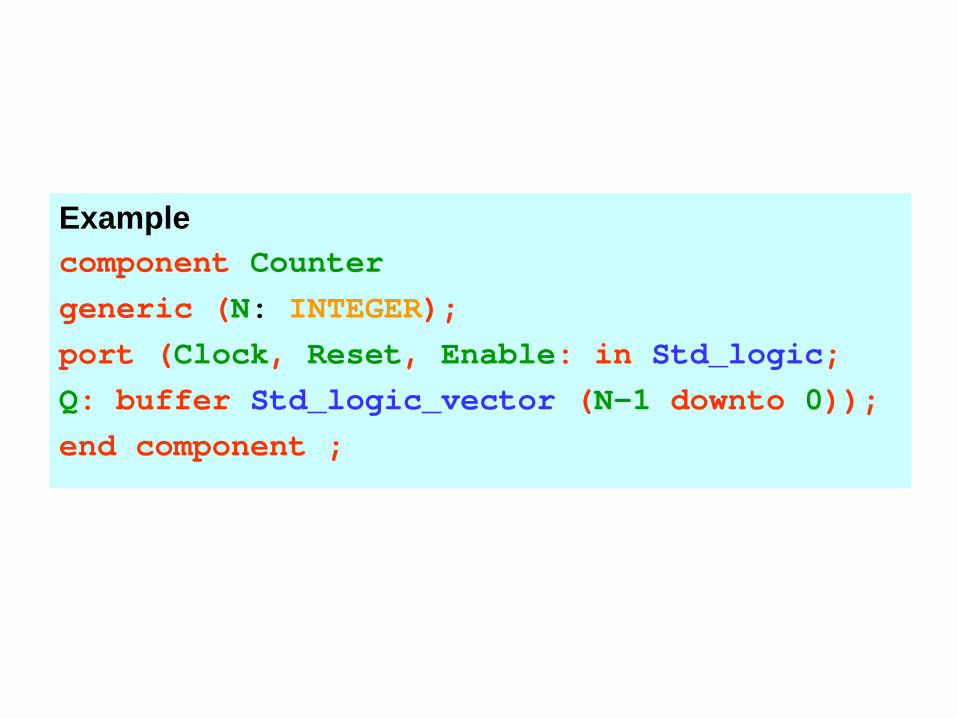
Examplecomponent Countergeneric (N: INTEGER);port (Clock, Reset, Enable: in Std_logic;Q: buffer Std_logic_vector (N-1 downto 0));end component ;
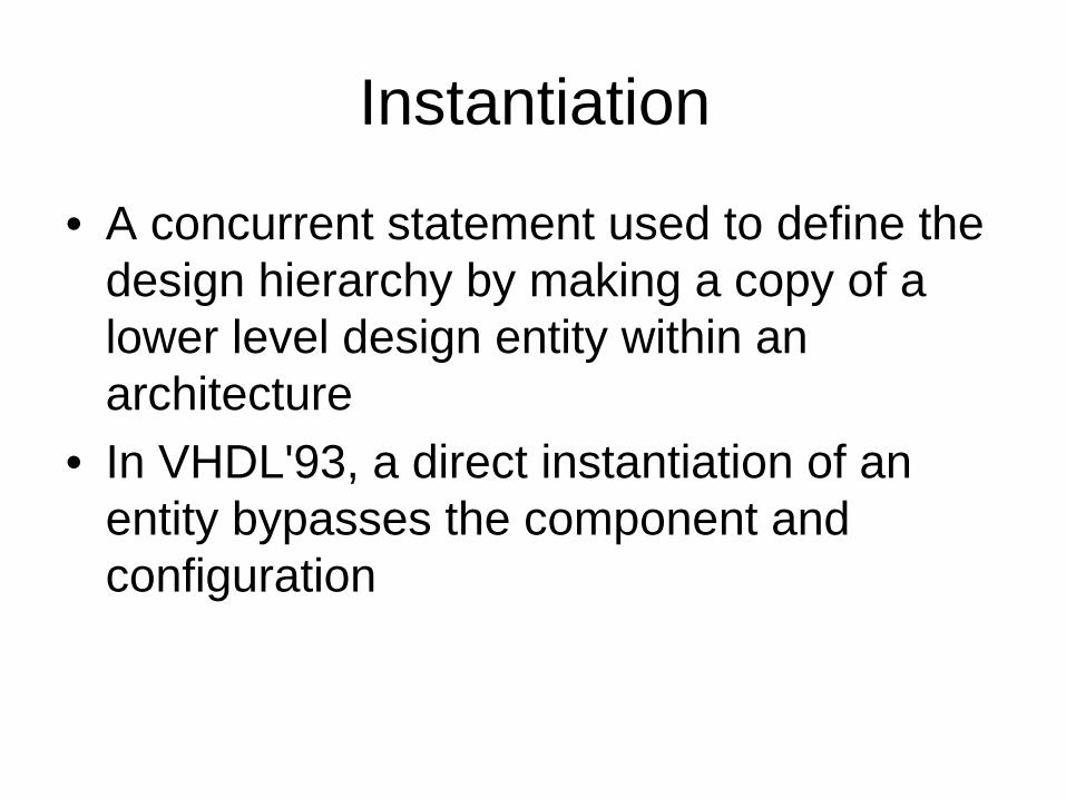
Instantiation
• A concurrent statement used to define the design hierarchy by making a copy of a lower level design entity within an architecture
• In VHDL'93, a direct instantiation of an entity bypasses the component and configuration

Syntax:InstanceLabel: [component] ComponentName
[GenericMap] [PortMap];InstanceLabel: entity
EntityName[(ArchitectureName)][GenericMap] [PortMap];
InstanceLabel: configuration ConfigurationName[GenericMap] [PortMap];
Where:architecture – begin - <HERE> - endblock – begin - <HERE> - endgenerate – begin - <HERE> - end

Rules:• An entity, architecture or configuration
must be compiled into a library before the corresponding instance can be compiled
• However, an instance of a component can be compiled before the corresponding design entity has even been written
Example :G1: NAND2 generic map (1.2 ns)
port map (N1, N2, N3);G2: entity WORK.Counter(RTL)
port map (Clk, Rst, Count);

Generic Map
• Used to define the values of generics• Usually given in an Instance, but may also
appear in a configuration
Syntaxgeneric map ([Formal =>] Actual, ...)
Formal = {either} Name FunctionCallActual = Expression

Where :Label : ComponentName <HERE> port map (…);for - use - <HERE> port map (…)block – generic (…); <HERE> ; port – begin - end
Rules :The two forms of syntax (ordered list or explicitly named choices) can be mixed, but the ordered list must come before the named choices
A generic map does not end with a semicolon!

Example:architecture Structure of Ent is
component NAND2generic (TPLH, TPHL: TIME := 0 NS);port (A, B: in STD_LOGIC;
F : out STD_LOGIC);end component;
beginG1: NAND2 generic map (1.9 NS, 2.8 NS)
port map (N1, N2, N3);G2: NAND2 generic map (TPLH => 2 NS, TPHL => 3 NS)
port map (N4, N5, N6);end Structure;

Port Map
• A port map is typically used to define the interconnection between instances in a structural description (or netlist)
• A port map maps signals in an architecture to ports on an instance within that architecture
• Port maps can also appear in a configuration or a block

Syntax:port map ([Formal =>] Actual, ...);
Formal = {either} Name FunctionCallActual = {either} Name FunctionCall open
Where:Label : ComponentName generic map (…) <HERE>;for - use - generic map (…) <HERE>;block - port (…) ; <HERE>; - begin - end

Rules:• The two forms of syntax (ordered list or explicitly named
ports) can be mixed, but the ordered list must come before the named ports
• Within an instance, the formals are ports on the component or entity being instanced, the actuals are signals visible in the architecture containing the instance
• Within a configuration, the formals are ports on the entity, the actuals are ports on the component
• If the actual is a conversion function, this is called implicitly as values are passed in
• If the formal is a conversion function, this is called implicitly as values are passed out
Use the port names rather than order to improve readability and reduce the risk of making connection errors

Example:component COUNTER
port (CLK, RESET: in Std_logic;UpDown: in Std_logic := '0' ;-- default valueQ: out Std_logic_vector(3 downto 0));
end component;...-- Positional association...G1: COUNTER port map (Clk32MHz, RST, open, Count);
-- Named association (order doesn't matter)...G2: COUNTER port map ( RESET => RST,CLK => Clk32MHz,Q(3) => Q2MHz,Q(2) => open, -- unconnectedQ(1 downto 0) => Cnt2,UpDown => open);

Top Level Entity and Lower Level Entity
TOP LEVEL ENTITY
Clk32MHz Q2MHz
Cnt2
RST
COUNT
COUNTER(LOWER LEVEL ENTITY)
CLK
RESET
QUpdown

TOP LEVEL ENTITY
Clk32MHz
Q2MHz
Cnt2
RST
COUNT
G1
CLK
RESET
Q
UpdownG2
CLK
RESET
Q(3)
Updown
Q(0)
CLK => Clk32MHzQ(3) => Q2MHz
UpDown => open
RESET => RST

A still simpler exampleentity ND4 is
port (in1,in2,in3,in4 : in std_logic ;z : out std_logic);
end ND4;architecture ND4_CI of ND4 iscomponent ND2
port (a , b : in std_logic;c : out std_logic);
end component ;signal temp1, temp2 : std_logic;beginU1 : ND2 port map (a => in1 , b => in2 , c => temp1);U2 : ND2 port map (a => in3 , b => in4 , c => temp2);U3 : ND2 port map (a => temp1 , b => temp2 , c => z);end ND4_CI ;

infers…ND4
U1
U3
U2
IN1
IN2
IN3
IN4
Z
a
a
b
b
a
b
c
c
c
c => temp1 for U1a => temp1 for U3
c => temp2 for U2b => temp2 for U3

Generate statement• A concurrent statement used to create
regular structures or conditional structures during elaboration
• Used to create multiple copies of components , processes or blocks
• It provides a compact description of regular structures such as memories , registers and counters

• Two flavours of generate statement are:– for … generate
• Number of copies is determined by a discrete range
– if … generate• Zero or one copy is made conditionally
• Range must be a computable integer in any of the following forms:– integer_expression to integer_expression– integer_expression downto integer_expression– Each integer_expression evaluates to an integer

Syntax :Label: for ParameterName in Range generate[Declarations...begin]ConcurrentStatements...
end generate [Label];
Label: if Condition generate[Declarations...begin]ConcurrentStatements...
end generate [Label];

Where:architecture – begin - <HERE> - endblock – begin - <HERE> - endgenerate – begin - <HERE> - end
Rules :• The Range and Condition must both be
static, i.e. they cannot include signals• The Label at the beginning of the generate
statement cannot be omitted
Synthesis:• Synthesis is straightforward, but not all
synthesis tools support generate!
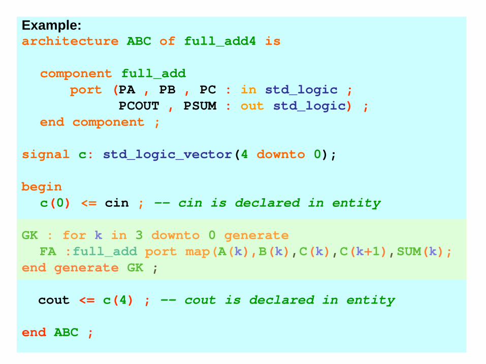
Example:architecture ABC of full_add4 is
component full_addport (PA , PB , PC : in std_logic ;
PCOUT , PSUM : out std_logic) ;end component ;
signal c: std_logic_vector(4 downto 0);
beginc(0) <= cin ; -- cin is declared in entity
GK : for k in 3 downto 0 generateFA :full_add port map(A(k),B(k),C(k),C(k+1),SUM(k);
end generate GK ;
cout <= c(4) ; -- cout is declared in entity
end ABC ;

infers…
FA2
A(2) B(2)
C(2)
SUM(2)
FA3
A(3) B(3)
Cout
SUM(3)
FA0
A(0) B(0)
CinC(1)
SUM(0)
FA1
A(1) B(1)
SUM(1)
C(3)

architecture SHIFTER_ARCH of SHIFTER is
component DFFport (D , CLK : in std_logic ;
Q : out std_logic) ;end component ;
begin
GK : for k in 0 to 3 generateGK0 : IF k=0 generate
DFILPFLOP : DFF port map (count , clock , Q(k));end generate GK0 ;GK1_3 : if k > 0 generate
DFILPFLOP : DFF port map (Q(k-1), clock , Q(k));end generate GK1_3 ;
end generate GK ;end SHIFTER_ARCH ;
Another example

infers…
DF1DF0 DF3DF2
CLOCK
COUNT
Q(0) Q(1) Q(2) Q(3)

Ways to describe a circuit!
• Three types of descriptions possible with VHDL– Structural– Dataflow– Behavioral

Structural Method• At the structural level, which is the lowest level, you
have to first manually design the circuit.• Use VHDL to specify the components and gates that
are needed by the circuit and how they are connected together by following your circuit exactly
• Synthesizing a structural VHDL description of a circuit will produce a netlist that is exactly like your original circuit
• The advantage of working at the structural level is that you have full control as to what components are used and how they are connected.
• But you need to first come up with the circuit and so the full capabilities of the synthesizer are not utilized

Dataflow Method• At the dataflow level, you use the built-in logical
functions of VHDL in signal assignment statements to describe a circuit, which again you have to first design manually
• Boolean functions that describe a circuit can be easily converted to signal assignment statements using the built-in logical functions
• The only drawback is that the built-in logical functions such as the AND and OR function only take two operands. This is like having only 2-input gates to work with !
All the statements use in the structural and dataflow level are executed concurrently

Behavioral Method• Describing a circuit at the behavioral level is
most similar to writing a computer program• You have all the standard high-level
programming constructs such as the FOR LOOP, WHILE LOOP, IF THEN ELSE, CASE, and variable assignments
• The statements are enclosed in a process block and are executed sequentially

Example
BCD to 7- segment display decoder
a
b
c
d
e
fg
BCD to 7-segmentdisplay decoder
I3I2I1I0
segs(6) {seg 'a'}segs(5) {seg 'b'}segs(4) {seg 'c'}segs(3) {seg 'd'}segs(2) {seg 'e'}segs(1) {seg 'f'}segs(0) {seg 'g'}

Truth-table

Logic Equations
2 1 0
3 1 2 0'
'2 1 0
' ' ' ' '1 0 2 0 2 1 2 1 0
' ' '1 0 2 0
' ' ' '3 2 1 2 0 1 0
'3 2 1 1 0
( )
( )
( )
a I I I I
b I I I
c I I I
d I I I I I I I I I
e I I I I
f I I I I I I I
g I I I I I
= + +
= +
= + +
= + + +
= +
= + + +
= + ⊕ +

Logic gates

Structural VHDL descriptionENTITY myxnor2 IS PORT(i1, i2: IN BIT;o: OUT BIT);END myxnor2;ARCHITECTURE Dataflow OF myxnor2 ISBEGINo <= not(i1 XOR i2);END Dataflow;
ENTITY myxor2 IS PORT(i1, i2: IN BIT;o: OUT BIT);END myxor2;ARCHITECTURE Dataflow OF myxor2 ISBEGINo <= i1 XOR i2;END Dataflow;
ENTITY myand2 IS PORT(i1, i2: IN BIT;o: OUT BIT);END myand2;ARCHITECTURE Dataflow OF myand2 ISBEGINo <= i1 AND i2;END Dataflow;

ENTITY myand3 IS PORT(i1, i2, i3: IN BIT; o: OUT BIT);END myand3;ARCHITECTURE Dataflow OF myand3 ISBEGINo <= (i1 AND i2 AND i3);END Dataflow;
ENTITY myor2 IS PORT(i1, i2: IN BIT;o: OUT BIT);END myor2;ARCHITECTURE Dataflow OF myor2 ISBEGINo <= i1 OR i2;END Dataflow;
ENTITY myor3 IS PORT(i1, i2, i3: IN BIT;o: OUT BIT);END myor3;ARCHITECTURE Dataflow OF myor3 ISBEGINo <= i1 OR i2 OR i3;END Dataflow;

ENTITY myor4 IS PORT(i1, i2, i3, i4: IN BIT; o: OUT BIT);END myor4;ARCHITECTURE Dataflow OF myor4 ISBEGINo <= i1 OR i2 OR i3 OR i4;END Dataflow;
ENTITY inv IS PORT (i: IN BIT; o: OUT BIT);END inv;ARCHITECTURE Dataflow OF inv ISBEGINo <= not i;END Dataflow;

LIBRARY ieee;USE ieee.std_logic_1164.all;ENTITY bcd IS PORT(i0, i1, i2, i3: IN BIT;a, b, c, d, e, f, g: OUT BIT);END bcd;ARCHITECTURE Structural OF bcd ISCOMPONENT inv PORT (i: IN BIT ;o: OUT BIT);END COMPONENT;COMPONENT myand2 PORT(i1, i2: IN BIT;o: OUT BIT);END COMPONENT;COMPONENT myand3 PORT(i1, i2, i3: IN BIT;o: OUT BIT);END COMPONENT;COMPONENT myor2 PORT(i1, i2: IN BIT;o: OUT BIT);END COMPONENT;COMPONENT myor3 PORT(i1, i2, i3: IN BIT;o: OUT BIT);END COMPONENT;COMPONENT myor4 PORT(i1, i2, i3, i4: IN BIT;o: OUT BIT);END COMPONENT;COMPONENT myxnor2 PORT(i1, i2: IN BIT;o: OUT BIT);END COMPONENT;COMPONENT myxor2 PORT(i1, i2: IN BIT;o: OUT BIT);END COMPONENT;

SIGNAL j,k,l,m,n,o,p,q,r,s,t,u,v,w,x,y,z: BIT;BEGINU1: INV port map(i2,j);U2: INV port map(i1,k);U3: INV port map(i0,l);U4: myXNOR2 port map(i2, i0, z);U5: myOR3 port map(i3, i1, z, a);U6: myXNOR2 port map(i1, i0, y);U7: myOR2 port map(j, y, b);U8: myOR3 port map(i2, k, i0, c);U9: myAND2 port map(i1, l, x);U10: myAND2 port map(j, l, w);U11: myAND2 port map(j, i1, v);U12: myAND3 port map(i2, k, i0, t);U13: myOR4 port map(x, w, v, t, d);U14: myAND2 port map(i1, l, s);U15: myAND2 port map(j, l, r);U16: myOR2 port map(s, r, e);U17: myAND2 port map(i2, k, q);U18: myAND2 port map(i2, l, p);U19: myAND2 port map(k, l, o);U20: myOR4 port map(i3, q, p, o, f);U21: myXOR2 port map(i2, i1, n);U22: myAND2 port map(i1, l, m);U23: myOR3 port map(i3, n, m, g);END Structural;

Dataflow VHDL descriptionLIBRARY ieee;USE ieee.std_logic_1164.all;
ENTITY bcd IS PORT (I: IN STD_LOGIC_VECTOR (3 DOWNTO 0);Segs: OUT std_logic_vector (1 TO 7));END bcd;
ARCHITECTURE Dataflow OF bcd ISBEGINSegs(1) <= I(3) OR I(1) OR NOT (I(2) XOR I(0)); -- seg aSegs(2) <= (NOT I(2)) OR NOT (I(1) XOR I(0)); -- seg bSegs(3) <= I(2) OR (NOT I(1)) OR I(0); -- seg cSegs(4) <= (I(1) AND NOT I(0)) OR (NOT I(2) AND NOT I(0)) -- seg dOR (NOT I(2) AND I(1)) OR (I(2) AND NOT I(1) AND I(0));
Segs(5) <= (I(1) AND NOT I(0)) OR (NOT I(2) AND NOT I(0)); -- seg eSegs(6) <= I(3) OR (I(2) AND NOT I(1)) -- seg fOR (I(2) AND NOT I(0)) OR (NOT I(1) AND NOT I(0));
Segs(7) <= I(3) OR (I(2) XOR I(1)) OR (I(1) AND NOT I(0)); -- seg gEND Dataflow;

Behavioral VHDL descriptionlibrary IEEE;use IEEE.STD_LOGIC_1164.all;entity BCD is
port( I : in STD_LOGIC_VECTOR(3 downto 0);segs : out STD_LOGIC_VECTOR(6 downto 0) );
end BCD;architecture Behavioral of BCD isbeginwith I selectSegs <= "1111110" when "0000",
"0110000" when "0001","1101001" when "0010","1111001" when "0011","0110011" when "0100","1011011" when "0101","1011111" when "0110","1110000" when "0111","1111111" when "1000", "1110011" when "1001","0000000" when others;
end Behavioral;

Output

Equations for carry_generate(G) and carry_propagate(P) for ALU 74181
Carry Lookahead Logic
xi
yi
xi-1
x0
yi-1
y0
c0
ci
hsi
si
gi = xi . yipi =xi + yi
ci+1 = gi + pi . ci
Assignment No 3

c1 = g0 + p0 . c0
c2 = g1 + p1 . g0 + p1 .p0 .c0
c3 = g2 + p2 . g1 + p2 .p1 .g0 +p2 .p1 .p0 .c0
c4 = g3 + p3 . g2 + p3 .p2 .g1 +p3 .p2 .p1 .g0 +p3 .p2 .p1 .p0 .c0
Additional Information

G_L= (g3 +p3 .g2 +p3 .p2 .g1 +p3 .p2 .p1 .g0 )’
P_L=(p3 .p2 .p1 .p0 )’
Implement the Carry_Generate and Carry_Propagate outputs also to complete the ALU assignment
Equations for implementation of G_L , P_L outputs

Sequential Statements
Next Class

‘generate’d doubt !
fulladder
GK.0.FA
fulladder
GK.3.FA
fulladder
GK.2.FA
fulladder
GK.1.FA
COUT[4]
SUM[3:0][3:0]
CinB[3:0] [3:0]
A[3:0] [3:0][0] PA[0] PB
PC[1]PCOUT[0]PSUM
[3] PA[3] PB[3] PC
[4]PCOUT[3]PSUM[2] PA
[2] PB[2] PC
[3]PCOUT[2]PSUM[1] PA
[1] PB[1] PC
[2]PCOUT[1]PSUM
fulladder
GK.3.FAfulladder
GK.0.FA
fulladder
GK.1.FA
fulladder
GK.2.FA
COUT[4]
SUM[3:0][3:0]
CinB[3:0] [3:0]
A[3:0] [3:0]
[3] PA[3] PB[3] PC
[4]PCOUT[3]PSUM
[0] PA[0] PB
PC[1]PCOUT[0]PSUM
[1] PA[1] PB[1] PC
[2]PCOUT[1]PSUM
[2] PA[2] PB[2] PC
[3]PCOUT[2]PSUM
GK : for k in 3 downto 0 generate GK : for k in 0 to 3 generate=

Sequential Statements
R.B.GhongadeLecture 12

Sequential Statements• VHDL code is inherently concurrent• Sections of code that are executed
sequentially are :– PROCESS– FUNCTION– PROCEDURE
• One important aspect of sequential code is that it is not limited to sequential logic
• We can build sequential circuits as well as combinational circuits
• Sequential code is also called behavioral code• Thus a PROCESS is a concurrent statement which
describes behaviour

• Sequential statements are allowed only inside PROCESSES, FUNCTIONS, or PROCEDURES
• Sequential statements are:– IF– WAIT– CASE– LOOP
• VARIABLES are also restricted to be used in sequential code only
VARIABLE can never be global, so its value can not be passed out directly

SIGNALS and VARIABLES revisited !
• VHDL has two ways of passing non-static values around: by means of a SIGNAL or by means of a VARIABLE
• A SIGNAL can be declared in a PACKAGE, ENTITY or ARCHITECTURE (in its declarative part), while a VARIABLE can only be declared inside a piece of sequential code
• SIGNAL is global while VARIABLE is local• The value of a VARIABLE can never be passed out of
the PROCESS directly; if necessary, then it must be assigned to a SIGNAL
• Update of VARIABLE is immediate whereas new value for SIGNAL is generally only guaranteed to be available after the conclusion of the present run of the PROCESS
• Assignment operator for SIGNAL is “<= “ while that for VARIABLE is “ : = “

Process
• A PROCESS is a sequential section of VHDL code
• It is characterized by the presence of IF, WAIT, CASE, or LOOP, and by a sensitivity list (except when WAIT is used)
• A PROCESS must be installed in the main code, and is executed every time a signal in the sensitivity list changes (or the condition related to WAIT is fulfilled)

Syntax
[label:] [postponed] PROCESS (sensitivity list)[VARIABLE name type [range] [:= initial_value;]]BEGIN(sequential code)END [postponed] PROCESS [label];
entity - begin - <HERE> - end architecture - begin - <HERE> - endblock - begin - <HERE> - endgenerate - begin - <HERE> - end
Where “POSTPONED” is a reserved VHDL word
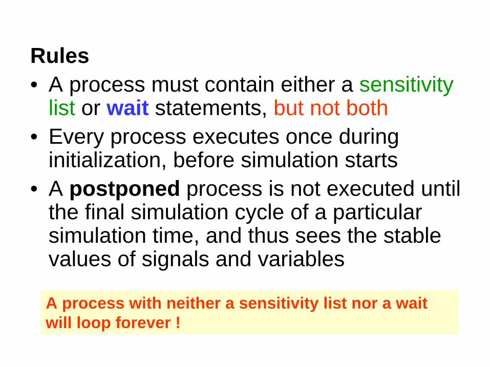
Rules• A process must contain either a sensitivity
list or wait statements, but not both• Every process executes once during
initialization, before simulation starts• A postponed process is not executed until
the final simulation cycle of a particular simulation time, and thus sees the stable values of signals and variables
A process with neither a sensitivity list nor a wait will loop forever !

• To construct a synchronous circuit, monitoring a signal (clock, for example) is necessary
• A common way of detecting a signal change is by means of the EVENT attribute
• For instance, if clk is a signal to be monitored, then clk ’ EVENT returns TRUE when a change on clk occurs (rising or falling edge)
Using EVENT attribute

IF construct• A sequential statement which executes one
branch from a set of branches dependent upon the conditions, which are tested in sequence
Syntax[Label:] if Condition thenSequentialStatements...[elsif Condition thenSequentialStatements...]... {any number of elsif parts}[elseSequentialStatements...]end if [Label];
Be careful about the spelling of elsif and end if

Synthesis• Assignments within if statements generally
synthesize to multiplexers• Incomplete assignments, where outputs remain
unchanged for certain input conditions, synthesize to transparent latches in unclocked processes, and to flip-flops in clocked processes
• In some circumstances, nested if statements synthesize to multiple logic levels. This can be avoided by using a case statement instead

• A set of elsif branches can be used to impart priority to the conditions tested first
• To decode a value without giving priority to certain conditions, use a case statement instead
ExampleIF (x<y) THEN temp:="11111111";ELSIF (x=y AND w='0') THENtemp := "11110000";ELSE temp:=(OTHERS =>'0');

D Flip-Flop with asynchronous reset
• A D-type flip-flop is the most basic building block in sequential logic circuits. In it, the output must copy the input at either the positive or negative transition of the clock signal (rising or falling edge)
If rst = ‘1’, then the output must be q = ‘0’ ,regardless of the status of clk. Otherwise, the output must copy the input (that is, q = d) at the positive edge of clk

LIBRARY ieee;USE ieee.std_logic_1164.all;
ENTITY dff ISPORT (d, clk, rst: IN STD_LOGIC;q: OUT STD_LOGIC);END dff;
ARCHITECTURE behavior OF dff ISBEGINPROCESS (clk, rst)BEGINIF (rst='1') THENq <= '0';ELSIF (clk'EVENT AND clk='1') THENq <= d;END IF;END PROCESS;END behavior;

Output
q
Rq
rst
clkd Q[0]D[0]

q
Rq
rst
clkd Q[0]D[0]
Changing the statementELSIF (clk'EVENT AND clk=‘0') THEN

One Digit counter example
Progressive 1-digit decimal counter (0 -> 9 ->0)
Single bit input (clk) and a 4-bit output (digit).

LIBRARY ieee;USE ieee.std_logic_1164.all;
ENTITY counter ISPORT (clk : IN STD_LOGIC; digit : OUT INTEGER RANGE 0 TO 9);END counter;
ARCHITECTURE counter OF counter ISBEGINcount: PROCESS (clk)VARIABLE temp : INTEGER RANGE 0 TO 10;BEGINIF (clk'EVENT AND clk='1') THENtemp := temp + 1;IF (temp=10) THEN temp := 0;END IF;END IF;digit <= temp;END PROCESS count;END counter;

Output
In a counter like circuits always use comparison statements with constant valuesThis ensures simple comparator inference as against full comparator inference for comparison with unknown values

digit[3:0]
clk
[3][30][1]
[32]
[3][30][1]
[32] un2_temp[29:32] +
count.un1_temp <
temp_3[1]
0
1
temp_3[3]
0
1
count.temp[3:0]
[3:0]
[29:32]1
[29:32]
1010 0
[1][31]
0
[3][29]
[3:0]Q[3:0]D[3:0]
[3]
[1][32]
[29]
[31:32]
[3]
[1][32] un2_temp[29:32]
+ count.un9_temp temp_3[1]
0
1
temp_3[3]
0
1
count.temp[3:0]
[3:0]
1
[0][31]
[29]
[31]
[1]0
[29]
[3]0
[3:0]Q[3:0]D[3:0]
digit[3:0]
clk
Changing the statement IF (temp>=10) THEN temp := 0;
Extra Hardware

Sequential Statements cont..
Next Class

Sequential Statements II
R.B.GhongadeLecture 13

Wait statement
• The operation of WAIT is sometimes similar to that of IF
• PROCESS cannot have a sensitivity list when WAIT is employed
• Three flavours of WAIT statements are:– WAIT UNTIL– WAIT ON– WAIT FOR

Syntax
WAIT UNTIL signal_condition;
• The WAIT UNTIL statement accepts only one signal, thus being more appropriate for synchronous code than asynchronous
• Since the PROCESS has no sensitivity list in this case, WAIT UNTIL must be the first statement in the PROCESS
• The PROCESS will be executed every time the condition is met

Example ( 8-bit register )
PROCESS -- no sensitivity listBEGINWAIT UNTIL (clk'EVENT AND clk='1');IF (rst='1') THENop <= "00000000";ELSIF (clk'EVENT AND clk='1') THENop <= inp;END IF;END PROCESS;

Output and Inference
op[7:0]
op[7:0][7:0]inp[7:0] [7:0]rst
clk[7:0]Q[7:0][7:0] D[7:0]
R
Output changes only with clk

Syntax
WAIT ON signal1 [, signal2, ... ];
• The WAIT ON statement accepts multiple signals
• The PROCESS is put on hold until any of the signals listed changes

Example ( 8-bit register )
PROCESSBEGINWAIT ON clk, rst;IF (rst='1') THENop <= "00000000";ELSIF (clk'EVENT AND clk='1') THENop <= inp;END IF;END PROCESS;

Output and Inference
op[7:0]
Rop[7:0][7:0]inp[7:0] [7:0]
rst
clk[7:0]Q[7:0][7:0] D[7:0]
Output changes with clk and rst

DFF revisited with WAIT!LIBRARY ieee;USE ieee.std_logic_1164.all;ENTITY dff ISPORT (d, clk, rst: IN STD_LOGIC; q: OUT STD_LOGIC);END dff;ARCHITECTURE dff OF dff ISBEGINPROCESSBEGINWAIT ON rst, clk;IF (rst='1') THENq <= '0';ELSIF (clk'EVENT AND clk='1') THENq <= d;END IF;END PROCESS;END dff;

Output and Inference
q
Rq
rst
clkd Q[0]D[0]
Infers exactly the same hardware as the earlier design
As a homework problem repeat the one digit counter with WAIT statement

Syntax
WAIT FOR time;
• WAIT FOR is intended for simulation only(waveform generation for test-benches)

Case statement• CASE is another statement intended exclusively
for sequential code• The CASE statement (sequential) is very similar
to WHEN (combinational)• All permutations must be tested, so the keyword
OTHERS is often helpful• Another important keyword is NULL (the
counterpart of UNAFFECTED), which should be used when no action is to take place
• CASE allows multiple assignments for each test condition while WHEN allows only one

[Label:] case Expression iswhen Choices =>
SequentialStatements...when Choices =>
SequentialStatements...... {any number of when parts}end case [Label];
Syntax
Choices = Choice | Choice | ...Choice = {either}
ConstantExpressionRangeothers {the last branch}

Whereprocess – begin - <HERE> - endfunction – begin - <HERE> - endprocedure – begin - <HERE> - endif – then - <HERE> - elsif – then - <HERE>- else - <HERE> - endcase - => - <HERE> - when - => - <HERE>- endloop-<HERE>-end

Rules• The Expression must not be enclosed in
parenthesis• The type of the Expression must be
enumeration, integer, physical, or a onedimensional array
• Every case of the Expression must be covered once and only once by theChoices

Synthesis• Assignments within case statements
generally synthesize to multiplexers• Incomplete assignments (i.e. where
outputs remain unassigned for certain input conditions) in unclocked processes synthesize to transparent latches
• Incomplete assignments in clocked processes synthesize to recirculation around registers

Examplecase ADDRESS iswhen 0 => -- Select a single valueA <= '1';when 1 =>A <= '1'; -- More than one statement in a
-- branchB <= '1';when 2 to 15 => -- Select a range of ADDRESS
-- valuesC <= '1';when 16 | 20 | 24 => -- Pick out several
-- ADDRESS valuesB <= '1';C <= '1';D <= '1';when others => -- Mop up the restnull;end case;
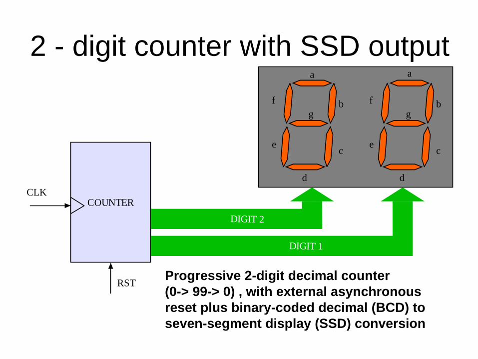
2 - digit counter with SSD output
COUNTER
a
b
c
d
e
fg
a
b
c
d
e
fg
DIGIT 1
7 BITS
CLK
RST
DIGIT 2
Progressive 2-digit decimal counter (0-> 99-> 0) , with external asynchronous reset plus binary-coded decimal (BCD) to seven-segment display (SSD) conversion

LIBRARY ieee;USE ieee.std_logic_1164.all;ENTITY counter IS
PORT (clk, rst : IN STD_LOGIC;digit1, digit2 : OUT STD_LOGIC_VECTOR (6 DOWNTO 0));
END counter;ARCHITECTURE counter OF counter ISBEGIN
PROCESS (clk, rst)VARIABLE temp1: INTEGER RANGE 0 TO 10;VARIABLE temp2: INTEGER RANGE 0 TO 10;
BEGINIF (rst='1') THEN
temp1 := 0;temp2 := 0;
ELSIF (clk'EVENT AND clk='1') THENtemp1 := temp1 + 1;IF (temp1=10) THEN
temp1 := 0;temp2 := temp2 + 1;
IF (temp2=10) THENtemp2 := 0;
END IF;END IF;
END IF;

CASE temp1 ISWHEN 0 => digit1 <= "1111110"; --7EWHEN 1 => digit1 <= "0110000"; --30WHEN 2 => digit1 <= "1101101"; --6DWHEN 3 => digit1 <= "1111001"; --79WHEN 4 => digit1 <= "0110011"; --33WHEN 5 => digit1 <= "1011011"; --5BWHEN 6 => digit1 <= "1011111"; --5FWHEN 7 => digit1 <= "1110000"; --70WHEN 8 => digit1 <= "1111111"; --7FWHEN 9 => digit1 <= "1111011"; --7BWHEN OTHERS => NULL;
END CASE;CASE temp2 IS
WHEN 0 => digit2 <= "1111110"; --7EWHEN 1 => digit2 <= "0110000"; --30WHEN 2 => digit2 <= "1101101"; --6DWHEN 3 => digit2 <= "1111001"; --79WHEN 4 => digit2 <= "0110011"; --33WHEN 5 => digit2 <= "1011011"; --5BWHEN 6 => digit2 <= "1011111"; --5FWHEN 7 => digit2 <= "1110000"; --70WHEN 8 => digit2 <= "1111111"; --7FWHEN 9 => digit2 <= "1111011"; --7BWHEN OTHERS => NULL;END CASE;
END PROCESS;END counter;

Output

Inference
DO NOT TRY TO WORK OUT HOW THIS CIRCUIT WORKS !!!

Test !!!
Next Class

Sequential Statements III
R.B.GhongadeLecture 14

Loop statement• LOOP is useful when a piece of code must
be instantiated several times• Like IF, WAIT, and CASE, LOOP is
intended exclusively for sequential code, so it too can only be used inside a PROCESS, FUNCTION, or PROCEDURE.
• There are several ways of using LOOP• A loop is an infinite loop (and thus an
error) unless it contains an exit or wait statement

FOR / LOOP: The loop is repeated a fixed number of times
[label:] FOR identifier IN range LOOP(sequential statements)END LOOP [label];
WHILE / LOOP: The loop is repeated until a condition no longer holds
[label:] WHILE condition LOOP(sequential statements)END LOOP [label];
[label:] LOOP(SequentialStatements)END LOOP [label];
Syntax

EXIT: Used for ending the loop
[label:] EXIT [label] [WHEN condition];
NEXT: Used for skipping loop steps
[label:] NEXT [loop_label] [WHEN condition];
WAIT : Continue looping until..

FOR i IN 0 TO 5 LOOPx(i) <= enable AND w(i+2);y(0, i) <= w(i);END LOOP;
The loop will be repeated unconditionally until i reaches 5 (that is, six times)
• One important remark regarding FOR / LOOP is that both limits of the range mustbe static
• Thus a declaration of the type "FOR i IN 0 TO choice LOOP", where choice is an input (non-static)parameter, is generally not synthesizable
Example of FOR / LOOP:

WHILE (i < 10) LOOPWAIT UNTIL clk'EVENT AND clk='1';(other statements)END LOOP;
In this example, LOOP will keep repeating while i < 10
Example of WHILE / LOOP:
LOOPWAIT UNTIL Clock = '1';EXIT WHEN Reset = '1';Div2 <= NOT Div2;END LOOP;
Example of WAIT in LOOP :

FOR i IN data'RANGE LOOPCASE data(i) ISWHEN '0' => count:=count+1;WHEN OTHERS => EXIT;END CASE;END LOOP;
Example of EXIT :
EXIT implies not an escape from the current iteration of the loop, but rather a definite exit (that is, even if i is still within the data range, the LOOP statement will be considered as concluded). In this case, the loop will end as soon as a value different from ‘0’ is found in the data vector

FOR i IN 0 TO 15 LOOPNEXT WHEN i=skip; -- jumps to next iteration(...)END LOOP;
Example with NEXT:
NEXT causes LOOP to skip one iterationwhen i = skip

Synthesis• Not generally synthesizable. Some tools
do allow loops containing wait statements to describe implicit finite state machines, but this is not a recommended practice

Example : 8-bit unsigned Carry Ripple Adder
+
a b
s
cin cout
+
a0 b0
c0 c1
s0
+
a1 b1
c2 +
a7 b7
s7
c8
s1
c7cin cout
a b
s
TOP LEVELLO
WER
LEVEL
sj = aj XOR bj XOR cjcj+1 = (aj AND bj ) OR (aj AND cj ) OR (bj AND cj )

LIBRARY ieee;USE ieee.std_logic_1164.all;ENTITY adder ISGENERIC (length : INTEGER := 8);PORT ( a, b: IN STD_LOGIC_VECTOR (length-1 DOWNTO 0);cin: IN STD_LOGIC; s: OUT STD_LOGIC_VECTOR (length-1 DOWNTO 0);cout: OUT STD_LOGIC);END adder;ARCHITECTURE adder OF adder ISBEGIN
PROCESS (a, b, cin)VARIABLE carry : STD_LOGIC_VECTOR (length DOWNTO 0);BEGIN
carry(0) := cin;FOR i IN 0 TO length-1 LOOPs(i) <= a(i) XOR b(i) XOR carry(i);carry(i+1) := (a(i) AND b(i)) OR (a(i) AND
carry(i)) OR (b(i) AND carry(i));END LOOP;
cout <= carry(length);END PROCESS;
END adder;

Output

Example: Leading ZerosThe circuit should count the
number of leading zeros in a binary vector, starting from
the left end
0 0 0 1 1 0 0 0
0123

LIBRARY ieee;USE ieee.std_logic_1164.all;ENTITY LeadingZeros ISPORT ( data: IN STD_LOGIC_VECTOR (7 DOWNTO 0);zeros: OUT INTEGER RANGE 0 TO 8);END LeadingZeros;ARCHITECTURE behavior OF LeadingZeros IS
BEGINPROCESS (data)
VARIABLE count: INTEGER RANGE 0 TO 8;BEGINcount := 0;FOR i IN data'RANGE LOOP
CASE data(i) ISWHEN '0' => count := count + 1;WHEN OTHERS => EXIT;
END CASE;END LOOP;zeros <= count;
END PROCESS;END behavior;

Output
Modify the design for trailing zeros !

Comparison between Concurrent and Sequential
Constructs
R.B.GhongadeLecture 15

CASE versus IF• Though in principle the presence of ELSE in the
IF/ELSE statement might infer the implementation of a priority decoder (which would never occur with CASE), this will generally not happen
• When IF (a sequential statement) is used to implement a fully combinational circuit, a multiplexer might be inferred instead
• Therefore, after optimization, the general tendency is for a circuit synthesized from a VHDL code based on IF not to differ from that based on CASE

Same inference !---- With IF: --------------IF (sel="00") THEN x<=a;ELSIF (sel="01") THEN x<=b;ELSIF (sel="10") THEN x<=c;ELSE x<=d;---- With CASE: ------------CASE sel ISWHEN "00" => x<=a;WHEN "01" => x<=b;WHEN "10" => x<=c;WHEN OTHERS => x<=d;END CASE;

CASE versus WHEN• CASE and WHEN are very similar. However,
while one is concurrent (WHEN), the other is sequential (CASE)
WHEN CASE Statement type Concurrent Sequential
Usage
Only outsidePROCESSES,FUNCTIONS, orPROCEDURES
Only inside PROCESSES, FUNCTIONS, or PROCEDURES
All permutations must be tested
Yes forWITH/SELECT/WHEN Yes
Max. # of assignments per test One Any
No-action keyword UNAFFECTED NULL

Same functionality !---- With WHEN: ----------------WITH sel SELECTx <= aWHEN "000",b WHEN "001",c WHEN "010",UNAFFECTED WHEN OTHERS;---- With CASE: ----------------CASE sel ISWHEN "000" => x<=a;WHEN "001" => x<=b;WHEN "010" => x<=c;WHEN OTHERS => NULL;END CASE;

Using Sequential Code to Design Combinational Circuits
• Sequential code can be used to implement either sequential or combinational circuits
• Registers are for sequential circuits necessary, so will be inferred by the compiler
• This should not happen for combinational circuits
• Also for a combinational circuit, the complete truth-table should be clearly specified in the code

Rules to be followed while using sequential code for designing combinational circuits
• Rule 1: Make sure that all input signals used (read) in the PROCESS appear in its sensitivity list
• Rule 2: Make sure that all combinations of the input/output signals are included in the code; that is, make sure that, by looking at the code, the circuit’s complete truth-table can be obtained (indeed, this is true for both sequential as well as concurrent code)

• Failing to comply with rule 1 will generally cause the compiler to simply issue a warning saying that a given input signal was not included in the sensitivity list, and then proceed as if the signal were included. Even though no damage is caused to the design in this case, it is a good design practice to always take rule 1 into consideration
• With respect to rule 2, however, the consequences can be more serious because incomplete specifications of the output signals might cause the synthesizer to infer latches in order to hold their previous values

Bad Combinational Design
x should behave as a multiplexer; that is, should be equal to the input selected by sel; y, on the other hand, should be equal to ‘0’ when sel = ‘‘00’’, or ‘1’ if sel = ‘‘01’’

LIBRARY ieee;USE ieee.std_logic_1164.all;ENTITY example ISPORT (a, b, c, d: IN STD_LOGIC; sel: IN INTEGER RANGE 0 TO 3;
x,y: OUT STD_LOGIC);END example;ARCHITECTURE example OF example ISBEGIN
PROCESS (a, b, c, d, sel)BEGIN
IF (sel=0) THENx<=a;y<=‘0’;
ELSIF (sel=1) THENx<=b;y<=‘1’;
ELSIF (sel=2) THENx<=c;
ELSEx<=d;
END IF;END PROCESS;
END example;

Output
Value of y remains ‘1’ which is not expected
Cure for the problem: y<='X'; must be included for other conditions of sel i.e. 2 & 3

Some templates for use!process (Inputs) -- All inputs in sensitivity listbegin... -- Outputs assigned for all input conditions... -- No feedbackend process; -- Gives pure combinational logic
process (Inputs) -- All inputs in sensitivity listbeginif Enable = '1' then... -- Latched actionsend if;end process; -- Gives transparent latches + logic

process (Clock) -- Clock only in sensitivity listbeginif Rising_edge(Clock) then -- Test clock edge only... -- Synchronous actionsend if;end process; -- Gives flipflops + logic
process (Clock, Reset) -- Clock and reset only in -- sensitivity list
beginif Reset = '0' then -- Test active level of
-- asynchronous reset... -- Asynchronous actionselsif Rising_edge(Clock) then -- Test clock edge
-- only... -- Synchronous actionsend if;end process; -- Gives flipflops + logic

process -- No sensitivity listbeginwait until Rising_edge(Clock);... -- Synchronous actionsend process; -- Gives flipflops + logic

Implementing RAM
• The circuit has a data input bus (data_in), a data output bus (data_out), an address bus (addr), plus clock (clk) and write enable (wr_ena) pins
• When wr_ena is asserted, at the next rising edge of clk the vector present at data_in must be stored in the position specified by addr
• The output, data_out, on the other hand, must constantly display the data selected by addr

LIBRARY ieee;USE ieee.std_logic_1164.all;ENTITY ram ISGENERIC ( bits: INTEGER := 8; -- # of bits per wordwords: INTEGER := 16); -- # of words in the memoryPORT ( wr_ena, clk: IN STD_LOGIC; addr: IN INTEGER RANGE 0 TO words-1;data_in: IN STD_LOGIC_VECTOR (bits-1 DOWNTO 0);data_out: OUT STD_LOGIC_VECTOR (bits-1 DOWNTO 0));END ram;ARCHITECTURE ram OF ram ISTYPE vector_array IS ARRAY (0 TO words-1) OFSTD_LOGIC_VECTOR (bits-1 DOWNTO 0);SIGNAL memory: vector_array;BEGIN
PROCESS (clk, wr_ena)BEGIN
IF (wr_ena='1') THENIF (clk'EVENT AND clk='1') THEN
memory(addr) <= data_in;END IF;
END IF;END PROCESS;data_out <= memory(addr);
END ram;

Output
ram1
memory[7:0]
data_out[7:0][7:0]data_in[7:0] [7:0]
addr[3:0] [3:0]
clkwr_ena
[3:0] RADDR[3:0][7:0] DATA[7:0]
[7:0]DOUT[7:0][3:0] WADDR[3:0]WE[0]CLK

Packages, Functions and Procedures
R.B.GhongadeLecture 16,17

Fundamental units of VHDL code
COVERED SO FAR

Packages• Frequently used pieces of VHDL code are usually written
in the form of COMPONENTS, FUNCTIONS, or PROCEDURES
• Such codes are then placed inside a PACKAGE and compiled into the destination LIBRARY
• Packages allow code partitioning, code sharing, and code reuse
• Besides COMPONENTS, FUNCTIONS, and PROCEDURES, it can also contain TYPE and CONSTANT definitions
• A package is split into a declaration and a body• The package declaration defines the external interface to
the package, the package body typically contains the bodies of any functions or procedures defined in the package declaration

Syntax{declaration}package PackageName isDeclarations...end [package] [PackageName];
{body}package body PackageName isDeclarations...end [package body] [PackageName];

• Where a function or procedure is placed in a package, the declaration and body must conform, i.e. the parameters must be identical between the two
• Only definitions placed in the package declaration are visible outside the package
REMEMBER THIS !
Common, shared declarations of types, subtypes, constants, procedures, functions and components are best put in a package

A simple package
LIBRARY ieee;USE ieee.std_logic_1164.all;
PACKAGE my_package ISTYPE state IS (st1, st2, st3, st4);TYPE color IS (red, green, blue);CONSTANT vec: STD_LOGIC_VECTOR(7 DOWNTO 0) := "11111111";END my_package;
The example above shows a PACKAGE called my_package. It contains only TYPE and CONSTANT declarations, so a PACKAGE BODY is not necessary

LIBRARY ieee;USE ieee.std_logic_1164.all;
PACKAGE my_package ISTYPE state IS (st1, st2, st3, st4);TYPE color IS (red, green, blue);CONSTANT vec: STD_LOGIC_VECTOR(7 DOWNTO 0) := "11111111";FUNCTION positive_edge(SIGNAL s: STD_LOGIC) RETURN BOOLEAN;END my_package;
PACKAGE BODY my_package ISFUNCTION positive_edge(SIGNAL s: STD_LOGIC) RETURN BOOLEAN ISBEGINRETURN (s'EVENT AND s='1');END positive_edge;END my_package;
Example
• This example contains, besides TYPE and CONSTANTdeclarations, a FUNCTION.
• Therefore, a PACKAGE BODY is now needed • This function returns TRUE when a positive edge occurs on clk

• Any of the PACKAGES in the previous examples can now be compiled, becoming then part of our work LIBRARY (or any other)
• To make use of it in a VHDL code, we have to add a new USE clause to the main code(USE work.my_package.all), as shown below:
LIBRARY ieee;USE ieee.std_logic_1164.all;USE work.my_package.all;
ENTITY... ...ARCHITECTURE......
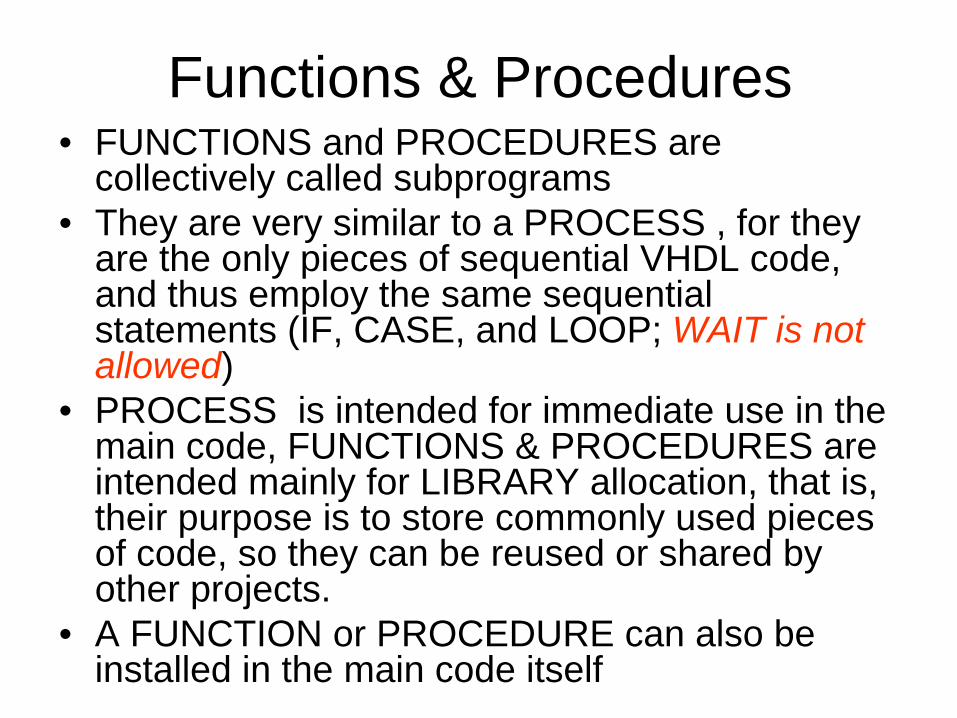
Functions & Procedures• FUNCTIONS and PROCEDURES are
collectively called subprograms • They are very similar to a PROCESS , for they
are the only pieces of sequential VHDL code, and thus employ the same sequential statements (IF, CASE, and LOOP; WAIT is not allowed)
• PROCESS is intended for immediate use in the main code, FUNCTIONS & PROCEDURES are intended mainly for LIBRARY allocation, that is, their purpose is to store commonly used pieces of code, so they can be reused or shared by other projects.
• A FUNCTION or PROCEDURE can also be installed in the main code itself

Functions
• Used to group together executable, sequential statements to define new mathematical or logical functions
• Also used to define bus resolution functions, operators, and conversion functions between data types
• When defined in a package, the function must be split into a declaration and a body
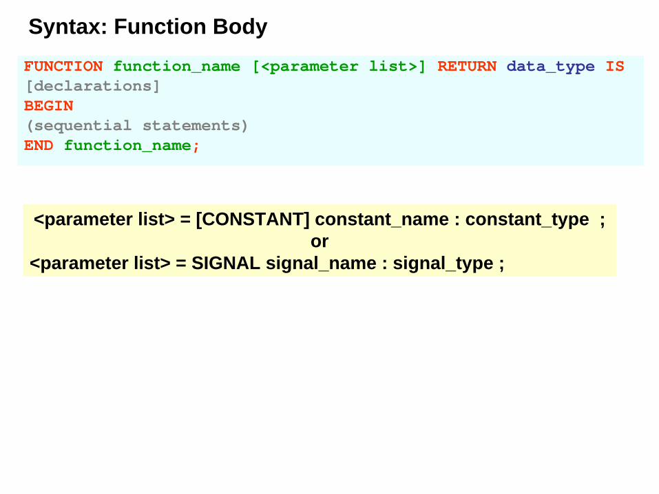
FUNCTION function_name [<parameter list>] RETURN data_type IS[declarations]BEGIN(sequential statements)END function_name;
<parameter list> = [CONSTANT] constant_name : constant_type ; or
<parameter list> = SIGNAL signal_name : signal_type ;
Syntax: Function Body

Where :(FUNCTION DECLARATION)
package - <HERE> - endpackage body - <HERE> - endentity – is - <HERE> - begin - endarchitecture –is - <HERE> - begin- endblock - <HERE> - begin - endgenerate - <HERE> - begin - endprocess - <HERE> - begin - endfunction – is - <HERE> - begin - endprocedure – is - <HERE> - begin - end
Function Body is NOT allowed inside a Package

Rules :• The function_name may be an identifier or
an operator• Functions cannot assign signals or
variables defined outside themselves, nor can then contain wait statements
• A function must execute a return statement
• Pure functions cannot have side effects - they must do nothing but return a value

• There can be any number of such parameters (even zero), can only be CONSTANT (default) or SIGNAL (VARIABLES are not allowed).
• Their types can be any of the synthesizable data types (BOOLEAN,STD_LOGIC, INTEGER, etc.)
• No range specification should be included (for example, do not enter RANGE when using INTEGER, or TO/DOWNTO when using STD_LOGIC_VECTOR)
• On the other hand, there is only one return value, whose type is specified by data_type

• The return type must be a name; it cannot include a constraint
• Variables defined inside a function are initialized each time the function is called
• The declaration and body must conform, i.e. the parameters and return type must be identical between the two
• The function declaration ends with a ";", whereas the function body has is at the corresponding point in the syntax
REMEMBER THIS !

Synthesis :• Each call to a function is synthesized as a separate
block of combinational logic
FUNCTION f1 (a, b: INTEGER; SIGNAL c: STD_LOGIC_VECTOR)RETURN BOOLEAN ISBEGIN(sequential statements)END f1;
Example :
• The function, named f1, receives three parameters (a, b, and c) • a and b are CONSTANTS (notice that the word CONSTANT can be
omitted, for it is the default object), while c is a SIGNAL. • a and b are of type INTEGER, while c is of type STD_LOGIC_VECTOR• Notice that neither RANGE nor DOWNTO was specified. • The output parameter (there can be only one) is of type BOOLEAN

Function Call• A function is called as part of an expression. The
expression can obviously appear by itself or associated to a statement (either concurrent or sequential)
x <= conv_integer(a); -- converts a to an integer-- (expression appears by -- itself)
y <= maximum(a, b); -- returns the largest of a -- and b
-- (expression appears by itself)IF x > maximum(a, b) ... -- compares x to the
-- largest of a, b-- (expression associated to a-- statement)
Examples of function calls:

Function positive_edge( )• The FUNCTION below detects a positive
(rising) clock edge. • It is similar to the
IF (clk’EVENT and clk = ‘1’) statement------ Function body: -----------------------------FUNCTION positive_edge(SIGNAL s: STD_LOGIC) RETURN
BOOLEAN ISBEGINRETURN (s'EVENT AND s='1');END positive_edge;------ Function call: -----------------------------...IF positive_edge(clk) THEN......

Function locations
FUNCTION/PROCEDURELOCATION
PACKAGE+
(PACKAGE BODY)
MAIN CODE
LIBRARY
ENTITY
ARCHITECTUREDECLARATIVE
PART

• Though a FUNCTION is usually placed in a PACKAGE (for code partitioning, code reuse, and code sharing purposes), it can also be located in the main code (either inside the ARCHITECTURE or inside the ENTITY)
• When placed in a PACKAGE, then a PACKAGE BODY is necessary, which must contain the body of each FUNCTION (or PROCEDURE) declared in the declarative part of the PACKAGE

FUNCTION Located in the Main CodeLIBRARY ieee;USE ieee.std_logic_1164.all;ENTITY dff ISPORT ( d, clk, rst: IN STD_LOGIC; q: OUT STD_LOGIC);END dff;ARCHITECTURE my_arch OF dff IS
FUNCTION positive_edge(SIGNAL s: STD_LOGIC)RETURN BOOLEAN IS
BEGINRETURN s'EVENT AND s='1';END positive_edge;
BEGINPROCESS (clk, rst)BEGIN
IF (rst='1') THEN q <= '0';ELSIF positive_edge(clk) THEN q <= d;END IF;
END PROCESS;END my_arch;
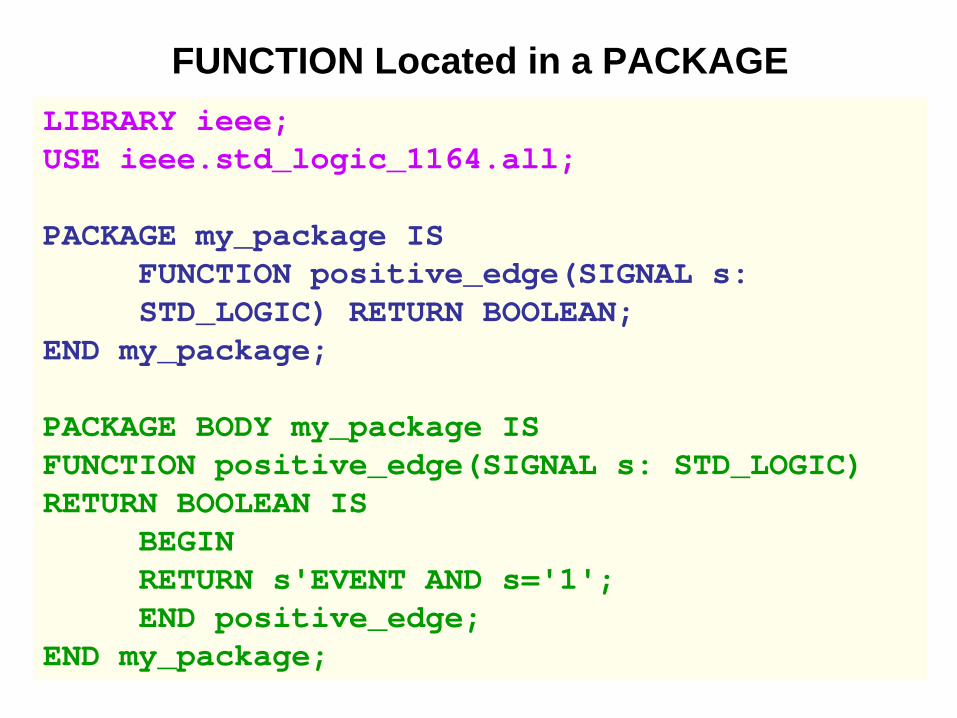
FUNCTION Located in a PACKAGELIBRARY ieee;USE ieee.std_logic_1164.all;
PACKAGE my_package ISFUNCTION positive_edge(SIGNAL s: STD_LOGIC) RETURN BOOLEAN;
END my_package;
PACKAGE BODY my_package ISFUNCTION positive_edge(SIGNAL s: STD_LOGIC)RETURN BOOLEAN IS
BEGINRETURN s'EVENT AND s='1';END positive_edge;
END my_package;

LIBRARY ieee;USE ieee.std_logic_1164.all;USE work.my_package.all;
ENTITY dff ISPORT ( d, clk, rst: IN STD_LOGIC;
q: OUT STD_LOGIC);END dff;
ARCHITECTURE my_arch OF dff ISBEGIN
PROCESS (clk, rst)BEGIN
IF (rst='1') THEN q <= '0';ELSIF positive_edge(clk) THEN q <= d;END IF;
END PROCESS;END my_arch;
WORK DESIGN SPACE SHOULD BE VISIBLE TO THE TOP-LEVEL ENTITY

Function conv_integer( )LIBRARY ieee;USE ieee.std_logic_1164.all;PACKAGE my_package IS
FUNCTION conv_integer (SIGNAL vector: STD_LOGIC_VECTOR) RETURN INTEGER;
END my_package;PACKAGE BODY my_package IS
FUNCTION conv_integer (SIGNAL vector: STD_LOGIC_VECTOR) RETURN INTEGER IS
VARIABLE result: INTEGER RANGE 0 TO 2**vector'LENGTH-1;BEGINIF (vector ( vector'HIGH )='1') THEN result:=1;ELSE result:=0;END IF;FOR i IN (vector'HIGH-1) DOWNTO (vector'LOW) LOOP
result:=result*2;IF(vector(i)='1') THEN result:=result+1;END IF;
END LOOP;RETURN result;END conv_integer;END my_package;
conv_integer( ) function convertsa STD_LOGIC_VECTOR value into an INTEGER value

Algorithm3 2 1 0
0 1 0 1 vector
Iteration 1:
vector’LENGTH=4vector’HIGH=3vector ( vector'HIGH )= 0
result=0 Since ‘ vector ( vector'HIGH )= 0 ’
3 downto 0 ( i = 2 to start with )
result= 0 x 2 result= 0 + 1 since vector(2)= 1
Iteration 2: ( i = 1)
result= 1 x 2 result= 2 + 0 since vector(1)= 0
Iteration 3: ( i = 0)
result= 2 x 2 result= 4 + 1 since vector(0)= 1
RETURNED : result = 5

LIBRARY ieee;USE ieee.std_logic_1164.all;USE work.my_package.all;
ENTITY conv_int2 ISPORT ( a: IN STD_LOGIC_VECTOR(0 TO 3);
y: OUT INTEGER RANGE 0 TO 15);END conv_int2;
ARCHITECTURE my_arch OF conv_int2 ISBEGIN
y <= conv_integer(a);END my_arch;

PROCEDURE
• A PROCEDURE is very similar to a FUNCTION and has the same basic purposes
• A procedure can return more than one value• Like a FUNCTION, two parts are necessary to
construct and use a PROCEDURE: – the procedure itself (procedure body) – procedure call

Procedure BodyPROCEDURE procedure_name [<parameter list>] IS[declarations]BEGIN(sequential statements)END procedure_name;
<parameter list> = [CONSTANT] constant_name: mode type;<parameter list> = SIGNAL signal_name: mode type; <parameter list> = VARIABLE variable_name: mode type;
• A PROCEDURE can have any number of IN, OUT, or INOUT parameters, which can be SIGNALS, VARIABLES, or CONSTANTS. For input signals (mode IN), the default is CONSTANT, whereas for output signals (mode OUT or INOUT) the default is VARIABLE
• WAIT, SIGNAL declarations, and COMPONENTS are not synthesizable when used in a FUNCTION. The same is true for a PROCEDURE, with the exception that a SIGNAL can be declared, but then the PROCEDURE must be declared in a PROCESS.
• Moreover, besides WAIT, any other edge detection is also not synthesizable with a PROCEDURE (that is, contrary to a function, a synthesizable procedure should not infer registers)

ExamplePROCEDURE my_procedure ( a: IN BIT; SIGNAL b,
c: IN BIT;SIGNAL x: OUT BIT_VECTOR(7 DOWNTO 0);SIGNAL y: INOUT INTEGER RANGE 0 TO 99) IS
BEGIN...END my_procedure;
• The PROCEDURE has three inputs, a, b, and c (mode IN) • a is a CONSTANT of type BIT, while b and c are SIGNALS, also
of type BIT. Notice that the word CONSTANT can be omitted for input parameters, for it is the default object (recall, however, that for outputs the default object is VARIABLE)
• There are also two return signals, x (mode OUT, type BIT_VECTOR) and y (mode INOUT, type INTEGER)
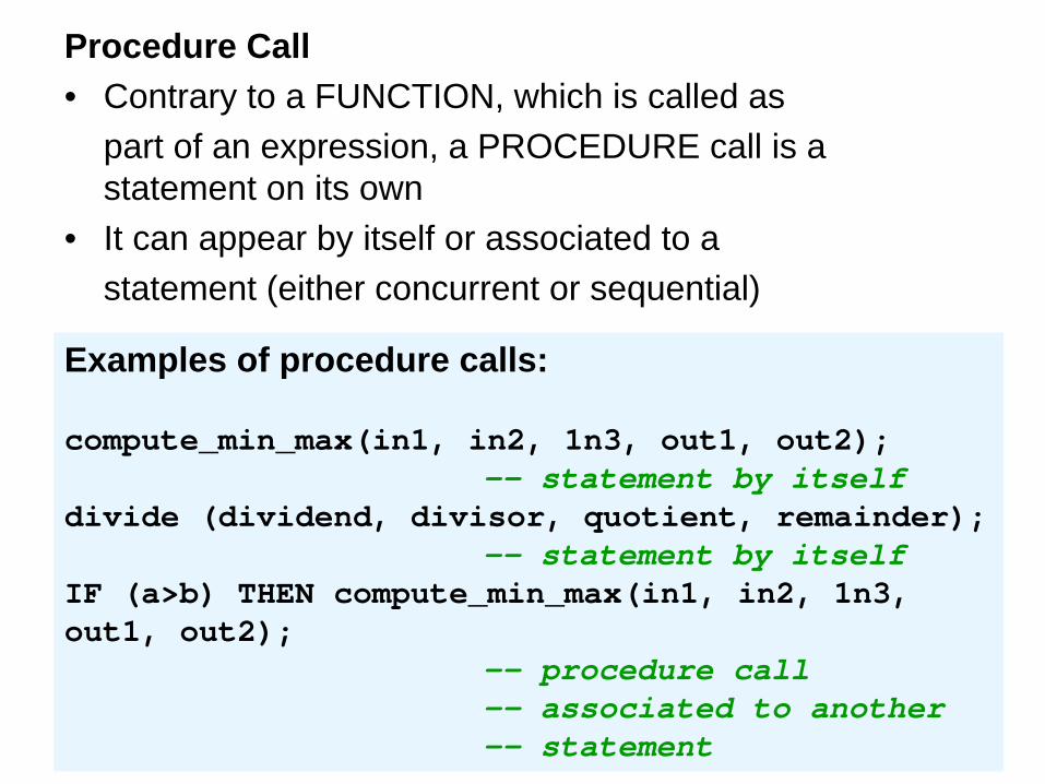
Procedure Call• Contrary to a FUNCTION, which is called as
part of an expression, a PROCEDURE call is a statement on its own
• It can appear by itself or associated to astatement (either concurrent or sequential)
Examples of procedure calls:
compute_min_max(in1, in2, 1n3, out1, out2);-- statement by itself
divide (dividend, divisor, quotient, remainder);-- statement by itself
IF (a>b) THEN compute_min_max(in1, in2, 1n3, out1, out2);
-- procedure call -- associated to another -- statement

SIMULATION ISSUES
R.B.GhongadeLecture 20,21,22

SIMULATION ISSUES
• SIMULATION• SIMULATION PROCESS• DELAY MODELING• TYPES OF SIMULATION

Simulation
• Simulation is a functional emulation of a
circuit design through software programs,
that use models to replicate how a device
will perform in terms of timing and results
Simulation
• Simulation eliminates the time-consuming need for constant physical prototyping
• Simulation can be performed during ALL stages of verification
• Motivation of simulation comes from the need to verify that the HDL code is correctly implementing the design
• Simply verify that the design meets its required specification

Flavours of Simulation
• Functional Simulation: Is functional verification of the design without any delays
• Pre- Layout simulation: Is functional verification of the design including logic cell delays
• Post- Layout simulation: Is performed after physical place and route( interconnect delays are taken into account)

Simulation at different Levels
a11
a22
3a3
4a4
b1
b2
b3
b4
5
6
7
8
Vcc10
GND0
a11
a223
a34a4
b1b2b3b4
5678
Vcc10
GND0
a11
a223
a34a4
b1b2b3b4
5678
Vcc10
GND0
a11
a223
a34a4
b1b2b3b4
5678
Vcc10
GND0
A
D
Q1
Q4
ENB
Register
Long card
Module Subsystem Chip System

Comparison for simulation
Module Subsystem Chip System
Stimuli DevelopmentSimulation Efficiency
Nature of detected problems
Bug correction time
Time in project
Difficult
Higher
Low level
Low
Early
Easier
Low
All kinds
Higher
Late

Steps in simulation
ELABORATION
INITIALISATION
EXECUTION

Steps in Simulation
• COMPILATION
* Checks VHDL source code to check syntax and semantic rules of VHDL
* If a syntax or semantic error occurs, then the compiler flags off an error message
* Else the compiler generates an intermediate code
SEMANTICS SYNTAX
SCIENCE OFMEANING
MECHANISMOF
LANGUAGE

Steps in Simulation cont...
• ELABORATION
* Ports are created for each instance of a component
* Memory storage is allocated for the required signal
* Interconnections among the port signals are specified
* Mechanism is established for executing the VHDL process in proper sequence

Steps in Simulation cont...
• INITIALIZATION
* Initial values preset in the declarations statements are assigned to signals/variables

Steps in Simulation cont...
* Every process is executed until it suspends. Signal values are updated only after this.
* Simulator accepts simulation commands like: RUN, ASSIGN,WATCH , which control the simulation of the system
• EXECUTION
* Simulation ends when all signals have been updated and new values have been assigned to the signals

SIMULATION PROCESS
BASIC DEFINITIONS
•EVENTA CHANGE ON COMPONENT OUTPUT THAT WILL BE PROPAGATED
•TRANSACTIONA CHANGE ON COMPONENT INPUT THAT DOES NOT PROPAGATE

SIMULATION PROCESS
BASIC DEFINITIONS cont.•SCHEDULING
FUTURE EVENTS GENERATED BY EVALUATION OF A PROCESS
•EVALUATION
CALCULATING THE OUTPUTS OF COMPONENTS BASED ON INPUTS AND CURRENT STATE
SIMULATION PROCESS
Time Jargon
Real Time Simulation Time(As it happens…) (Relative to some arbitrary t=0)
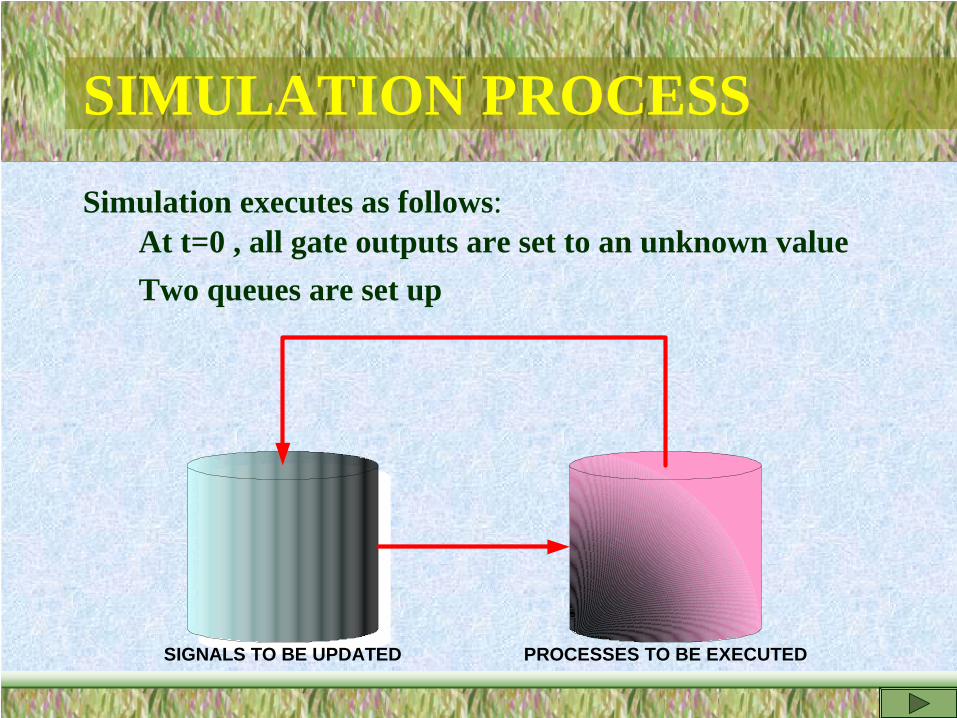
SIMULATION PROCESS
Simulation executes as follows:At t=0 , all gate outputs are set to an unknown valueTwo queues are set up
SIGNALS TO BE UPDATED PROCESSES TO BE EXECUTED

SIMULATION PROCESS
• When Simulation time is incremented :• Signal is updated• All processes sensitive to that signal are
placed on the process execution queue• Each resumed process is executed until it suspends• Effects of the logic changes that have
occurred as a result of process execution are evaluated
• Simulation time is set to the next event in queue or halted if simulation time gets exhausted
One loop iscalled DELTA
CYCLE

SIMULATION DELTA
• What is simulation delta?•Several logic changes occur simultaneously in a circuit (concurrent operations)•But simulator being run by a sequential machine, hence it cannot process events concurrently.•To take care this, time is frozen within the simulator.
•The real time the simulator takes to complete all concurrent operations in the queue is called SIMULATION DELTA

SIMULATION DELTA
t=0 ns t=1 ns
Zero simulation time
t=2 ns t=3 ns t=4 ns
Many delta cycles can occur
Real TimeThe minimum time interval possible for the simulator is assumed to be 1 ns here

SIMULATION DELTA
• SUMMARY
Simulation deltas allow ordering of events that occur at the same simulation time during simulation
Simulation deltas are infinitesimal amount of time used as synchronism mechanism when zero delay events are present

DELAY MODELING
Delays are timing parameters given by the user for modeling physical characteristics of hardware
Types of delays
INERTIAL DELAY TRANSPORT DELAY
Delays are specified in signal assignment statements onlyDelays should NOT be used in variable assignments

INERTIAL DELAY
• It is used to model the inherent inertia of physical devices
• Example:– The input value must be stable for a specified
minimum pulse duration before the value is allowed to propagate to the output
– If the input is not stable for the specified limit, no output change occurs

TRANSPORT DELAY
• It represents pure propagation delay i.e., wires and interconnect delays
• Signal value is assigned with a specified delay independent of the width of the input waveform

DELAYS
10 ns 3 ns
10 ns
2 ns
6 ns
X
Z1
Z2
Z3

TYPES OF SIMULATION
• FUNCTIONAL SIMULATION• BEHAVIORAL SIMULATION• STATIC TIMING SIMULATION• GATE-LEVEL SIMULATION• SWITCH-LEVEL SIMULATION• TRANSISTOR-LEVEL OR CIRCUIT-
LEVEL SIMULATION

TYPES OF SIMULATION
• FUNCTIONAL SIMULATIONIt ignores timing aspectsVerifies only the functionality of the design
• BEHAVIORAL SIMULATIONA given functionality is modeled using HDL
Timing aspects are considered

TYPES OF SIMULATION
• STATIC TIMING SIMULATIONA built in tool that computes delay for each timing pathDoes not require input stimuli
• GATE-LEVEL SIMULATIONIs used to check the timing performance of design
Delay parameters of logic cells are used to verify things

TYPES OF SIMULATION
• SWITCH-LEVEL SIMULATIONIs one level below the gate level simulation
It models transistors as switches
It provides more accurate timing predictions than gate-level simulation

TYPES OF SIMULATION
• TRANSISTOR-LEVEL SIMULATIONRequires transistor models. Circuit is described in terms of resistances, capacitances and voltage and current sourcesA set of mathematical equations relating current and voltages is setup and solved numerically
Gives analog results and is most accurate
Requires large amount of computing resources

And finally!!
Simulation time depends on :
• Simulation levels of logic
• Physical Memory of PC
• Speed of PC

THANK YOU !!!

Test benches in VHDL
Copyright, R.B.Ghongade
R.B.GhongadeLecture 18,19

• A design is always incomplete without verification
• There are several ways to verify VHDL designs
• Test benches are one of them• Test benches are also called Test cases
Introduction
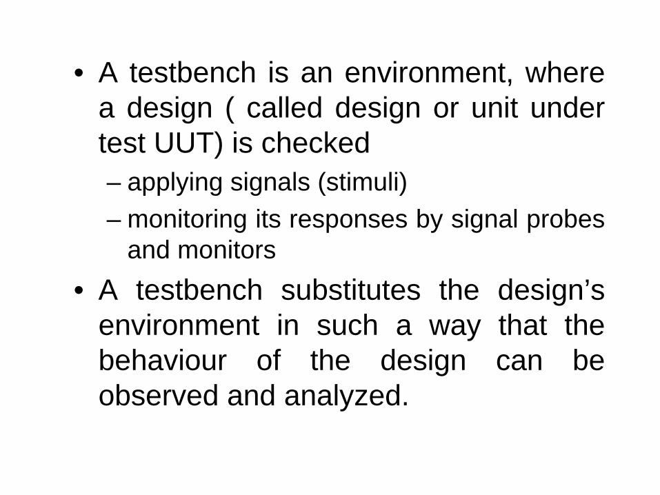
• A testbench is an environment, where a design ( called design or unit under test UUT) is checked – applying signals (stimuli) – monitoring its responses by signal probes
and monitors• A testbench substitutes the design’s
environment in such a way that the behaviour of the design can be observed and analyzed.

A testbench always consists of following elements:– a socket for the unit under test (UUT)– a stimuli generator (a subsystem that
applies stimuli to UUT, either generating them internally or reading from an external source)
– tools for observing UUT responses to the stimuli

Concept of Testbench

• A VHDL test bench is just another specification with its own
• entity • architecture
• In addition, it has special structure with some elements that are characteristic to this type of specification:
• Test bench entity has no ports,• UUT component instantiation - the relationship
between the test bench and UUT is specified through component instantiation and structural-type specification,
• Stimuli - it is a set of signals that are declared internally in the test bench architecture and assigned to UUT's ports in its instantiation. The stimuli are defined as waveforms in one or more behavioral processes.
Elements of a VHDL Test Bench


Using Test Benches• The design must be verifiable. • It is much more convenient to use a test bench for design
verification. • Writing a test bench -> very complex task • Therefore some guidelines for future stimuli development
should be written as you progress with the design.• It is the test bench which is simulated, not the unit under test. • The UUT is only one of the components instantiated in a test
bench. • There is no limitation on the test bench size.• The only limitation is the VHDL simulator used capability.

DESIGN
VERIFICATIONThe design process consists of design and verification phases The objective of the first one is to create a new VHDL specification that meets the system requirements.
Design Specification
Stimuli Definitions
Test bench Specifications
Test bench Simulation
Simulation of the test bench is the last phase of a design process. Here you will receive an answer to the question; "does the system behave as expected?" Remember that the answer received from simulating test bench is reliable only to the extent determined by the test bench accuracy and coverage area. The better a test bench is, the more confident you can be that your system is properly designed.
Writing stimuli can be performed concurrently with writing specifications for each new design block. The stimuli set should contain such set of input (and state) signal values that covers as much real life situations as possible.
When stimuli are specified, a test bench specification can be written It will contain the stimuli and an instantiation of the designed system (unit under test). It is the test bench and not design that will be simulated during the verification phase.

Example : Multiplexer

Example : J-K FlipFlop

Closer look at TestbenchUUT: 2- bit Multiplexer

Testbench

Waveforms

Testbench : Using assert…report

Waveforms

Error Report

SUMMARY
• A Test bench thus is an effective built- in tool for verifying VHDL designs•Troubleshooting becomes easier and faster because of the ASSERT…REPORT clause•Automation of verification is possible because of the seamless integration of language elements.

Synthesis Issues
R.B.GhongadeLecture 19

Agenda
• What is synthesis ?• Synthesis Tools : Expectations• Synthesis Tools : Features• Hardware modeling examples• Good coding Practices• Synthesis guidelines

What is synthesis ?
• Synthesis is an automatic process that converts user’s hardware description into structural logic description
• When we use VHDL as textual file, the process is called VHDL Synthesis
• Synthesis is a means of converting HDL into real world hardware
• Synthesis tools generate a gate-level netlist for the target technology

What is synthesis ?
x <= ( a and b ) or ( c and d );
SYNTHESIS = TRANSLATION + OPTIMIZATION
a
b
c
d
x
a
b
c
d
xLUT
a
b
c
d
x
• Synthesis is target device technology specific• Synthesizer will try to use the best architectural
resource available with the target

Several steps work out behind the scene!
• Translation ( language synthesis ) : Design at higher level of description is compiled into known language elements
• Optimization : Algorithms are applied to make the design compact and fast
• Design is mapped using architecture specific techniques
Translation
Optimization
MappingHardware Description - written with hardware in mind
Mix of Boolean , other operations and memory elements
Gate Level – Technology Specific

Synthesis process – design flowHDL behavioral description
RTL SynthesisRTL Optimization
High-leveldescription with
Boolean equations
Netlist
Logic extraction
StructuredBoolean equations
Logic Optimization
StructuredBoolean equations
Technology mappingGate-level
optimization
Optimized Netlist
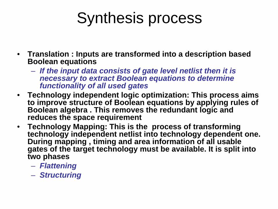
• Translation : Inputs are transformed into a description based Boolean equations– If the input data consists of gate level netlist then it is
necessary to extract Boolean equations to determine functionality of all used gates
• Technology independent logic optimization: This process aims to improve structure of Boolean equations by applying rules of Boolean algebra . This removes the redundant logic and reduces the space requirement
• Technology Mapping: This is the process of transforming technology independent netlist into technology dependent one. During mapping , timing and area information of all usable gates of the target technology must be available. It is split into two phases– Flattening– Structuring
Synthesis process

Flattening• The aim is to generate Boolean equations for each
output of module in such a way that the output value is a direct function of inputs. These equations reflect two level logic in SOP form.
• Resulting equations do not imply any structure• Good optimization results are obtained• Caution: In case of structured logic this process would
destroy the characteristic structure and its associated properties . e.g. carry look ahead adder
• Flattening cannot be applied to every logic circuit because the number of product terms may become very large

Structuring
• New intermediate variables are inserted during the structuring process
• E.g. If (A’.B’.C’) occurs 10 times then the tool may assign X= (A’.B’.C’) and use X everywhere
• Finally , the sub-functions are substituted into original equations
• Compared to the logic before structuring, the resulting area is reduced

Synthesis process- review
SYNTHESIS
DESIGN
CONSTRAINT(area , speed)
LIBRARIES
NETLIST REPORT
•Translation process converts RTL to a Boolean form•Optimization is done on the converted Boolean equations•Optimized logic is mapped to technology library
•Flattening is a process where all the design hierarchy is removed, the entire design is transformed into a flat , generic , SOP form•Structuring is the opposite of flattening, its adds structure to the generic design by extracting common logic factors and representing them as intermediate nodes to produce compact logic

Synthesis tool : expectations
A good synthesis tool should– perform technology specific optimizations i.e. vendor
specific FPGAs and CPLds– have best optimization techniques– allow designer control– have broad language coverage– provide user friendly debugging environment– have fast compile times– provide clean and seamless link with backend tools
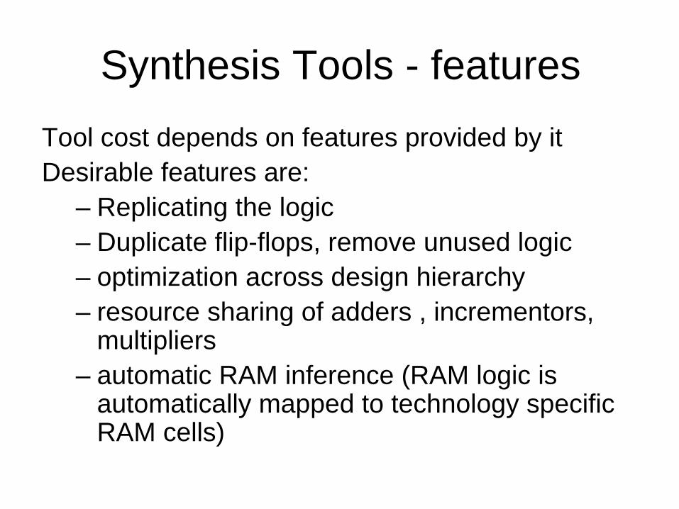
Synthesis Tools - featuresTool cost depends on features provided by itDesirable features are:
– Replicating the logic– Duplicate flip-flops, remove unused logic– optimization across design hierarchy– resource sharing of adders , incrementors,
multipliers– automatic RAM inference (RAM logic is
automatically mapped to technology specific RAM cells)

Replicate logic
– Replicate logic to meet fan-out demands
– E.g. WR’ may be connected to 100 points hence add buffers to split internally
BUF
BUF
BUF
BUF
BUF
BUF

Duplicating logic• We can duplicate the logic which generates the
signal , for minimizing fan-out• Trade-off : Loading effect of signals is reduced
hence lowering propagation delay but at the cost of logic and interconnect complexity
D Q D Q
D Q

Resource sharing• Some synthesis tools automatically perform a
limited amount of resource sharing ( for arithmetic expressions that are mutually exclusive)
• Consider the code:ADDSEL: process( sel, a ,b,c,d)
beginif (sel=‘1’ ) then
y<= a + b ;else
y<= c + d ;end if ;
end process ADDSEL ;

Resource sharing
+
a
b
+
c
d
sel
+y
a
c
b
d
sel
y
Before resource sharing
After resource sharing
An adder requires more floor space than a multiplexer
Simulation vs. Synthesis
• Some simulation constructs are not supported by synthesis tools– e.g. wait statements
• Synthesis tools ignore initial values• Care should be taken so that simulation-
synthesis mismatch does not occur

Using Signals or Variables• Variables are used only for convenience of
describing behaviour• Variables are used and declared in a process
however it cannot be used to communicate between processes
• Variable assignments are done immediately and are executed sequentially
• Variables may or may not represent physical wires
• Signal assignments are done at the end of process
• Signals represent physical wires in the circuit

• Use variables in combinational processes because there is less simulation overhead
• Order dependency– Signal assignments are order independent– Variable assignments are order dependent– Signal assignments under a clocked process are
translated into registers– Variable assignments under a clocked process may
or may not be translated into registers
Using Signals or Variables

process (clk, a, b, c, d)variable y, x, w : std_logic ;begin
if (clk=‘1’ and clk’event) thenz1<= y ;y : = x ;x : = a and b ;w : = c and d ;z2<= w ;end if;
end process ;
Signals or Variables
variables are read before being written to , this infers a memory element

Hardware inferred

Same process with order of statements changed
process (clk, a, b, c, d)variable y, x, w : std_logic ;begin
if (clk='1' and clk'event) thenx := a and b ;y := x ;z1<= y ;z2<= w ;w := c and d ;
end if;end process ;
variables are read before being written to , this infers a memory element

Hardware inferred
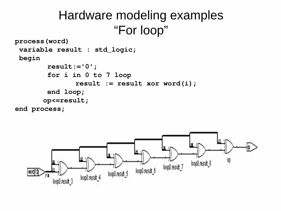
Hardware modeling examples “For loop”
process(word)variable result : std_logic;begin
result:='0';for i in 0 to 7 loop
result := result xor word(i);end loop;op<=result;
end process;

Multiplexer optimization
case sel iswhen “000” => y<= data(0);when “001” => y<= data(1);when “010” => y<= data(2);when “011” => y<= data(3);
1) when others => y<= ‘0’;2) when others => y<= ‘Z’;3) when others => y<= ‘X’;4) when others => NULL;
end case;
The hardware inferred depends on the condition given in the “when others” clause

Case 1when others => y<= ‘0’;
Case 2when others => y<= ‘Z’;

Case 3when others => y<= ‘X’;
Case 4when others => NULL;

Good coding practices• Good coding style means that the synthesis tool can
identify constructs within your code that it can easily map to technology features
• All programmable devices may have their unique architectural resources e.g. Xilinx Virtex series has built-in RAM
• Coding for performance :– common mistake is to ignore hardware and start
coding as if programming. To achieve best performance the designer must think about hardware
Good coding practices
• Improve performance by – avoiding unnecessary priority structures
in logic– optimizing logic for late arriving signals– structuring arithmetic for performance– avoiding area inefficient code– buffering high fan-out signals
• Use “constants” to enhance readability and code maintenance
• Comparison with a constant is preferred since it is much “cheaper” to implement
• To avoid accidental latches– specify all clauses of “if” and “case” statements– specify all outputs
• Use “case” rather than “if-then-else” whenever possible
• Use parentheses for better operation• Never use mode “buffer”
Good coding practices

Design constraints
• Constraining designs:– constraints are means of communicating our
requirements to the synthesis and back-end tools• Categories of constraints are :
– Timing constraints• maximum frequency• duty cycle• input delays• output delays
– Layout constraints

Design constraints
• Avoid over-constraining the design• Consequences of over-constraining are:
– Design performance suffers:• critical timing paths get the best placement and
fastest routing options• as the number of critical paths increase , the ability
to obtain the design performance objectives decrease
– Run times increase

Synthesis guidelines
• Simulate your design before synthesis• Avoid combinational loops in processes• If a port is declared to be an integer data
type, the range should be specified, else the synthesis tool will infer a 32-bit port
• Avoid mixed clock edges– if a large number of both positive and
negative edge flip-flops are required they should be placed in different modules

Synthesis guidelines
• For best results:– use technology primitives (macros) from the target
technology libraries wherever possible– try small designs on target technology to find its
limitations and strengths– Partition the design correctly
• eliminate glue logic at the top level• partition block size based on the logic function, CPU
resources and memory• separate random logic from structured logic• separate timing-sensitive modules from area -sensitive ones

CPLDs and FPGAs
Next class