introduction to photoemission and application...
TRANSCRIPT

introduction to photoemission and application to layered oxides
Amal al-Wahish
Advance Solid state 672
Instructor: Elbio Dagotto
Spring 2009
Department of Physics and Astronomy,
University of Tennessee
(Dated: March 21, 2009)
Abstract
In this work we look at the introduction to photoemission and application to layered oxides
and it’s importance in the fields of surface science and condensed-matter. We present a historical
introduction about photoemission , then review the general application of ARPES on layered
oxides, and finally, we quote some modern applications.
1

I. INTRODUCTION
Modern photoelectron spectroscopy (PS), which often called ”photoemission”, offer a
powerful widely-used way to study the properties of atoms, molecules, solids and surfaces[1,
2]. It is interesting to take a quick look at the history and demonstrate of the various stages
of photoemission development.
A. Historical Introduction
Historically, the inspiration for Photoemission original essay came from Hertz works. In
1887 Hertz observed that a spark between two electrodes occurs more easily if the negative
electrode is illuminated by UV radiation[3]. A few years later J.J. Thompson demonstrated
that the effect was due to emission of electrons by the electrode while under illumination.
The correct interpretation of this effect was given by Einstein (who was awarded the Nobel
Prize in 1921 especially for his photoemission work). He postulated that light was composed
of discrete quanta of energy E, this energy being proportional to ν, the frequency of the
light. This energy, minus (φ+EB) (where φ, the material work function, is measure of the
potential barrier at the surface that prevents the valance electrons from escaping and the
Binding energy )required to escape the solid, is taken up by the photoemitted electron, which
thus escapes with a maximum kinetic energy hν−φ,(φ for metals is typically around 4-5 eV
for metals) [3, 4]. In recent years the energy resolution of this method has been improved
considerably, namely for experiments using UV radiation to about 1meV, and in addition
the energy resolution for experiments employing soft x-rays (15 keV) has reached values of
about 50 meV. Where the X-ray Photoelectron spectroscopy(XPS) can be described with
the three-step model:
1. Absorption of the x-ray inside the solid.
2.Transport of the excited photoelectron to the surface.
3. Escape of the photoelectron from the surface[5]. These Models will be explain briefly
later.
This powerful method is relatively straight forward and allows to determine the energy
and the momentum of electrons. The fundamental experiment in the photoelectron spec-
troscopy involves exposing the specimen to be studied to a flux of nearly monoenergetic
2
radiation with mean energy E = hν, and then observing the resultant emission of photo-
electrons, and determine the kinetic energies of the electrons[1]. These steps can be done
by using the Angular Resolved Photoemission Spectroscopy which provides rich informa-
tion about the electron structure of crystals and of their surfaces[6].The following section
demonstrated the ARPES.
B. Angle resolved Photoemission Spectroscopy
In the last two decades, angle-resolved photoemission spectroscopy (ARPES) has emerged
as the most powerful probe of the momentum-resolved electronic structure of materials. This
achievement has largely been due to the construction of new sources for synchrotron radiation
and due to the extreme progress in the field of spectrometer design. The photoelectron
spectrometers provide very high energy, momentum resolution at a single electron emission
angle, and automated angle scanning techniques also facilitate a full hemisphere mapping of
the electron distribution in momentum space. As a consequence, ARPES has now become
a powerful imaging technique providing very direct k-space images of band dispersions as
well as of constant energy surfaces. Moreover, in combination with synchrotron radiation
as a tuneable photon source the experimental restrictions of ARPES regarding full k-space
accessibility are strongly relaxed and it is possible to study three-dimensional electronic
structures in great detail. In spite of the enormous potential of ARPES, however, there
remains one disadvantage: the spatial resolution of the technique is generally limited to
the spot size of modern light sources, i.e., generally to a few 100µm. As one of the most
important trends of photoemission spectroscopy, future efforts will tend to push down this
limit by some orders of magnitude in order to be able to study the electronic properties of
materials in the nanometer regime[4, 6].
In this work the experimental technique of photoemission imaging will be introduced and
its accuracy will be discussed.
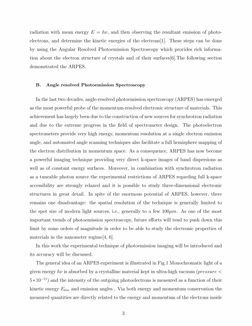
The general idea of an ARPES experiment is illustrated in Fig.1 Monochromatic light of a
given energy hν is absorbed by a crystalline material kept in ultra-high vacuum (pressure <
5∗10−11) and the intensity of the outgoing photoelectrons is measured as a function of their
kinetic energy Ekin and emission angles . Via both energy and momentum conservation the
measured quantities are directly related to the energy and momentum of the electrons inside
3
the crystal.
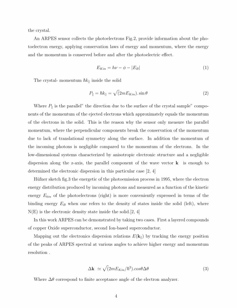
An ARPES sensor collects the photoelectrons Fig.2, provide information about the pho-
toelectron energy, applying conservation laws of energy and momentum, where the energy
and the momentum is conserved before and after the photoelectric effect.
EKin = hν − φ− |EB| (1)
The crystal- momentum ~k|| inside the solid
P‖ = ~k|| =√
(2mEKin). sin θ (2)
Where P‖ is the parallel” the direction due to the surface of the crystal sample” compo-
nents of the momentum of the ejected electrons which approximately equals the momentum
of the electrons in the solid. This is the reason why the sensor only measure the parallel
momentum, where the perpendicular components break the conservation of the momentum
due to lack of translational symmetry along the surface. In addition the momentum of
the incoming photons is negligible compared to the momentum of the electrons. In the
low-dimensional systems characterized by anisotropic electronic structure and a negligible
dispersion along the z-axis, the parallel component of the wave vector k is enough to
determined the electronic dispersion in this particular case [2, 4]
Hufner sketch fig.3 the energetic of the photoemission process in 1995, where the electron
energy distribution produced by incoming photons and measured as a function of the kinetic
energy Ekin of the photoelectrons (right) is more conveniently expressed in terms of the
binding energy EB when one refers to the density of states inside the solid (left), where
N(E) is the electronic density state inside the solid.[2, 4]
In this work ARPES can be demonstrated by taking two cases. First a layered compounds
of copper Oxide superconductor, second Ion-based superconductor.
Mapping out the electronics dispersion relations E(k‖) by tracking the energy position
of the peaks of ARPES spectral at various angles to achieve higher energy and momentum
resolution .
∆k '√
(2mEKin/~2).cosθ∆θ (3)
Where ∆θ correspond to finite acceptance angle of the electron analyzer.
4
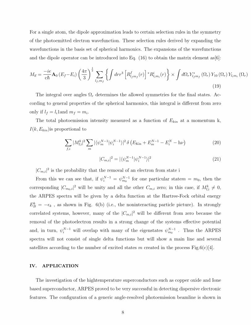
II. A SUMMARY OF THREE STEP MODEL
The three step model developed on ARPES from solid by Berglund and Spicer. This
model breaks up the EP process into three steps, the three step model is sketched by
Hufner fig.4. The photocurrent is decomposed into three separate factors: the probability of
excitation in the bulk solid, the probability of scattering of the excited electron on its path to
the surface by the atoms constituting the solid, and the probability of transmission through
the surface potential barrier for its final acceptance in the detector[6]. The optical excitation
of the electron in the bulk contains the all information about the intrinsic electronic structure
of the material.Travel of the excited electron to the surface can be described in terms of
an effective mean free path, proportional to the probability that the excited electron will
reach the surface without inelastic scattering processes, this processes determine the surface
sensitivity of the photoemission, where The suitability of PS to surface studies of materials is
essentially due to the short inelastic attenuation length of the photoelectrons in the sample,
as shown in Fig.5, where the so called universal curve for electron attenuation lengths in a
large number of elemental samples as a function of electron kinetic energy is shown[? ]. Also
the scattering process give rise to a continuous background in the spectra which is usually
ignored or subtracted. The Escape of the photoelectron into vacuum, is described by a
transmission probability through the surface, which depends on the energy of the excited
electron as well as the material work function φ. the photoelectron wave function can be
expressed as
ψ(r) =
∫dr′Gr(r, r′)VI (r′) ψi (r
′) (4)
where Vi describes the perturbation of the external light, ψi is the initial state one-electron
wave function of energy Ei, and is the Green function of the solid at the photoelectron energy
Ei + ~ω ,
Gr(r, r′) =∑f
ψf∗ (r′)ψf (r)
Ei + ~ω − Ef + iδ(5)
5
III. GOLDEN RULE
A. Linear response in the external field
The Hamiltonian of one electron in a system described by a potential V (r), to which an
external electromagnetic field is applied
H =p2
2m+ V (r)− e
2m[A(r).p+ p.A(r)] +
e2
2m|A(r)|2 (6)
where p is the electronic momentum operator.A(r) is the vector potential associated with
the field. A common choice is to work in the Coulomb gauge, in which
∇.A(r) = 0 (7)
Actually when the ultraviolet being used the momentum and the electromagnetic vector
potential are commute
(A(r).p+ p.A(r)) = i~∇.A(r) = 0 (8)
The interaction potential VI can thus be expressed as
VI(r) = − e
m[A(r).p] +
e2
2m|A(r)|2 (9)
The interaction with the photon is treated as a perturbation given by
Hint = − e
m[A(r).p] (10)
For low intensities of the external field, first order perturbation theory can be used to
study the interaction between the electromagnetic radiation and the system. Thus, applying
the Golden Rule to calculate the photocurrent, we obtain:
I(f) = |Mif| 2 = |〈ψf |VI |ψi〉|2 (11)
The most important approximations introduced in the theoretical formalism are the restric-
tion to a one-electron picture, and the use of only first-order perturbation theory to calculate
the interaction between the incident radiation and the system. The latter approximation is
equivalent to neglecting terms of order ≈ |A|2 in the calculation of the photocurrent, so the
term of order ≈ |A|2 in the interaction potential VI is omitted. This approximation remains
6

valid provided that the flux of incident photons is relatively low. The matrix element Mif
after keeping only the lowest-order terms can be written as:
Mif = 〈ψf |Hint|ψi〉 =ie~mc〈ψf |A(r).∇|ψi〉 (12)
B. Dipole approximation
Dipole approximation is theoretical description of the interaction between the electro-
magnetic field and the system. The dipole approximation assumes that the variation of
the external field A(r) is small in the spatial region in which the matrix element Mif is not
negligible. the external electromagnetic field is periodic in space, it can be expressed as:
A(r) = A0e eik·r = A0e(1 + ik · r + . . .) (13)
where A0 is the complex amplitude of the field (a scalar number), e is a unitary vector
in the direction of the light polarization, and k is a vector pointing in the propagation
direction of the field. The dipole approximation consists in keeping only the first term
of this expansion in the calculation of the photocurrent via Eq. (11) (it is assumed that
|kr| 1)[6].
The matrix element in the dipole approximation can be written as
Mif =ie~mc
A0 〈ψf |e.∇|ψi〉 (14)
the momentum operator p can be written as the commutator of two other operators
p = −i~∇ =−im
~[r, H0] (15)
Hence, if ψi and ψf are eigenstates of the Hamiltonian H0, the length form of the matrix
element Mif can be calculated
Mif =−iec~
A0 (Ef − Ei)〈ψf |e.r|ψi〉 (16)
A third form, known as the acceleration form of the matrix element:
Mif =−ie~mc
A0
(Ef − Ei)〈ψf |e.(∇.V )|ψi〉 (17)
To find these matrices, the following identity has been used
〈ψf |∇|ψi〉 =1
(Ef − Ei)〈ψf |[H,∇]|ψi〉 =
−1
(Ef − Ei)〈ψf |∇V |ψi〉 (18)
7
For a single atom, the dipole approximation leads to certain selection rules in the symmetry
of the photoemitted electron wavefunction. These selection rules derived by expanding the
wavefunctions in the basis set of spherical harmonics. The expansions of the wavefunctions
and the dipole operator can be introduced into Eq. (16) to obtain the matrix element as[6]:
Mif =−iec~
A0 (Ef−Ei)(
4π
3
) 12 ∑lf ,mf
∫drr3
[Rflfmf
(r)]∗Ri
limi(r)
×∫dΩrY
∗lfmf
(Ωr)Y10 (Ωr)Ylimi(Ωr)
(19)
The integral over angles Ωr determines the allowed symmetries for the final states. Ac-
cording to general properties of the spherical harmonics, this integral is different from zero
only if lf = li1and mf = mi.
The total photoemission intensity measured as a function of Ekin at a momentum k,
I(k,Ekin)is proportional to∑f,i
|Mkf,i|2∑m
|〈ψN−1m |ψN−1
i 〉|2 δ(EKin + EN−1
m − ENi − hν
)(20)
|Cm,i|2 = |〈ψN−1m |ψN−1
i 〉|2 (21)
|Cm,i|2 is the probability that the removal of an electron from state i
From this we can see that, if ψN−1i = ψN−1
m0for one particular statem = m0, then the
corresponding |Cm0,i|2 will be unity and all the other Cm,i zero; in this case, if Mkf,i 6= 0,
the ARPES spectra will be given by a delta function at the Hartree-Fock orbital energy
EkB = −εk , as shown in Fig. 6(b) (i.e., the noninteracting particle picture). In strongly
correlated systems, however, many of the |Cm,i|2 will be different from zero because the
removal of the photoelectron results in a strong change of the systems effective potential
and, in turn, ψN−1i will overlap with many of the eigenstates ψN−1
m0. Thus the ARPES
spectra will not consist of single delta functions but will show a main line and several
satellites according to the number of excited states m created in the process Fig.6(c)[4].
IV. APPLICATION
The investigation of the hightemperature superconductors such as copper oxide and Ione
based superconductor, ARPES proved to be very successful in detecting dispersive electronic
features. The configuration of a generic angle-resolved photoemission beamline is shown in
8
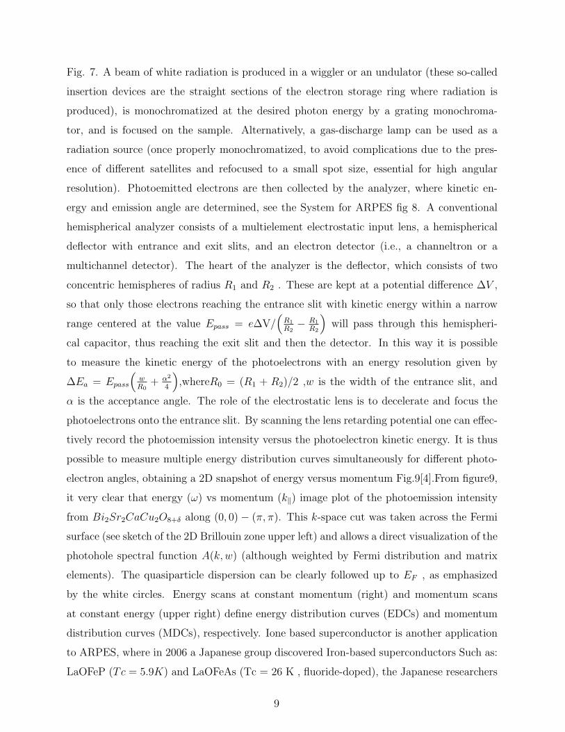
Fig. 7. A beam of white radiation is produced in a wiggler or an undulator (these so-called
insertion devices are the straight sections of the electron storage ring where radiation is
produced), is monochromatized at the desired photon energy by a grating monochroma-
tor, and is focused on the sample. Alternatively, a gas-discharge lamp can be used as a
radiation source (once properly monochromatized, to avoid complications due to the pres-
ence of different satellites and refocused to a small spot size, essential for high angular
resolution). Photoemitted electrons are then collected by the analyzer, where kinetic en-
ergy and emission angle are determined, see the System for ARPES fig 8. A conventional
hemispherical analyzer consists of a multielement electrostatic input lens, a hemispherical
deflector with entrance and exit slits, and an electron detector (i.e., a channeltron or a
multichannel detector). The heart of the analyzer is the deflector, which consists of two
concentric hemispheres of radius R1 and R2 . These are kept at a potential difference ∆V ,
so that only those electrons reaching the entrance slit with kinetic energy within a narrow
range centered at the value Epass = e∆V/(R1
R2− R1
R2
)will pass through this hemispheri-
cal capacitor, thus reaching the exit slit and then the detector. In this way it is possible
to measure the kinetic energy of the photoelectrons with an energy resolution given by
∆Ea = Epass
(wR0
+ α2
4
),whereR0 = (R1 + R2)/2 ,w is the width of the entrance slit, and
α is the acceptance angle. The role of the electrostatic lens is to decelerate and focus the
photoelectrons onto the entrance slit. By scanning the lens retarding potential one can effec-
tively record the photoemission intensity versus the photoelectron kinetic energy. It is thus
possible to measure multiple energy distribution curves simultaneously for different photo-
electron angles, obtaining a 2D snapshot of energy versus momentum Fig.9[4].From figure9,
it very clear that energy (ω) vs momentum (k‖) image plot of the photoemission intensity
from Bi2Sr2CaCu2O8+δ along (0, 0)− (π, π). This k-space cut was taken across the Fermi
surface (see sketch of the 2D Brillouin zone upper left) and allows a direct visualization of the
photohole spectral function A(k, w) (although weighted by Fermi distribution and matrix
elements). The quasiparticle dispersion can be clearly followed up to EF , as emphasized
by the white circles. Energy scans at constant momentum (right) and momentum scans
at constant energy (upper right) define energy distribution curves (EDCs) and momentum
distribution curves (MDCs), respectively. Ione based superconductor is another application
to ARPES, where in 2006 a Japanese group discovered Iron-based superconductors Such as:
LaOFeP (Tc = 5.9K) and LaOFeAs (Tc = 26 K , fluoride-doped), the Japanese researchers
9
discovered earlier (August 2008), that a new class of iron-based superconducting materials
also had much higher transition temperatures than the conventional low-temperature su-
perconductors. SmO0.9F0.1FeAs , being 55 K. In September 2008, Shens group studied the
electronic structure of LaOFeP. The purpose of this study was to understand the nature of
the ground state of the parent compounds LaOFeP, and to reveal the important differences
between Iron Oxypnictide and Copper based superconductors, all these study was depend
on ARPES technique, graph 10 show the powerful of this technique compar to theoretical
approach, Local-density approximations (LDA).
V. CONCLUSION AND SUMMARY
1-The photoemission process from a core level can be described as the photoexcita-
tion from a single atom, followed by the transport of the photoelectron on its way to the
detector.2- Angle resolve photoemission spectroscopy (ARPES) aka. k-space microscopy is
a direct measurement of the quasiparticle band dispersion , i.e. energy versus momentum.3-
The ARPES technique: a-By measuring the K.E and angular distribution of the electrons
photoemitted from a sample illuminated, one can gain information on both, the energy
and momentum.b-Very useful for detecting bands and Fermi Surface c-Gives us information
about the bulk and surface electronic structure and superconductor gap of materials. d-
Provides us direct and valuable information about the electronic states of a solid. e-Allows
us to compare directly with the theory. f-One can have high resolution information on both
energy and momentum.
[1] C. Fadley, Basic Cncept of X-ray Photoelectron Spectroscopy (Dapartment of Chemistry, Uni-
versity of Hawaii, Honolulu, Hawaii, 1978).
[2] S. Hufner, Very High Resolution Photoelectron Spectroscopy,Lecture Notes in Physics 715
(Springer, Berlin, Heidelberg, 2007), 1st ed.
[3] P. Y. Y. M. Cardona, Fundementals of Semiconductors physics and Materials properties
(Springer, Berline, Germany, 2005), 3rd ed.
[4] Z.-X. S. Andrea Damascelli, Zahid Hussain, Reviews of Modern Physics 75, 473 (2003).
10

[5] A. K. Frank de Groot, Core level Spectroscopy of Solids (CRC Press, Taylor and Francies
Group, USA, 1964), 1st ed.
[6] M. A. H. Wolfgang Schattke, Solid-State Photoemission and related Methods, theory and ex-
periment (WiLey-Vch GmbH and Co.KGaA, Weinheim, Germany, 2003), 1st ed.
11

FIG. 1: In ARPES, measuring the energy and momenta (mass times velocity) of electrons ejected
from a sample struck by energetic photons makes it possible to calculate the electrons’ initial energy
and momenta, and from this determine the sample’s electronic structure.
FIG. 2: The ARPES sensor now sits inside the vacuum chamber. This picture was taken before it
was completely built.
12

FIG. 3: The ARPES sensor, displayed as ”Spectrum” in blue, displays the intensity of detected
electrons, N(E), that have various kinetic energies, E. These values obtained by the ARPES sensor
correspond to the actual values of the ”Sample”, displayed red. In a solid material, the electrons
are distributed to an energy level below EFermi, the Fermi Level. The ARPES spectrum reveals
peaks with an identical energy distribution as the one in the solid. However, the peaks are slightly
wider, due to electron scattering during the process.
13
FIG. 4: Pictorial representation of three-step and one-step model descriptions of the photoemission
process.
FIG. 5: Illustration of the universal curve for electron attenuation in solids as a function of electron
kinetic energy
14

FIG. 6: Angle-resolved photoemission spetroscopy: (a) geometry of an ARPES experiment in
which the emission direction of the photoelectron is specified by the polar (q) and azimuthal (w)
angles; (b) momentum-resolved one-electron removal and addition spectra for a noninteracting
electron system with a single energy band dispersing across EF ; (c) the same spectra for an
interacting Fermi-liquid system (Sawatzky, 1989; Meinders, 1994). For both noninteracting and
interacting systems the corresponding groundstate (T50 K) momentum distribution function n(k)
is also shown. (c) Lower right, photoelectron spectrum of gaseous hydrogen and the ARPES
spectrum of solid hydrogen developed from the gaseous one (Sawatzky, 1989).
FIG. 7: Generic beamline equipped with a plane grating monochromator and a Scienta electron
spectrometer (Color).
15

FIG. 8: Photoemission Spectroscopy’s system, Mannella’s lab,UTK.
16

FIG. 9: Energy (ω) vs momentum k|| image plot of the photoemission intensity from
Bi2Sr2CaCu2O8+δ along (0, 0)-(π, π). This k-space cut was taken across the Fermi surface (see
sketch of the 2D Brillouin zone upper left) and allows a direct visualization of the photohole
spectral function A(k, v) (although weighted by Fermi distribution and matrix elements). The
quasiparticle dispersion can be clearly followed up to EF , as emphasized by the white circles. En-
ergy scans at constant momentum (right) and momentum scans at constant energy (upper right)
define energy distribution curves (EDCs) and momentum distribution curves (MDCs), respectively.
FIG. 10: Comparison between angle-resolved photoemission spectra and LDA band structures
along two high-symmetry lines. ARPES data from LaOFeP (image plots) were recorded using
42.5-eV photons with an energy resolution of 16 meV and an angular resolution of 0.3u
17