introduction to pcb designing with orcad 9
TRANSCRIPT
8/13/2019 Introduction to PCB Designing With OrCAD 9
http://slidepdf.com/reader/full/introduction-to-pcb-designing-with-orcad-9 1/9
Introduction to PCB Designing with orCAD v.9.2+
orCAD Family Release 9.2 (by Cadence) is a collection of several CAD software.
e.g.
Capture
and
Capture
CIS
–
for
schematic
drawings
Pspise – for simulation
Layout Plus and Layout Engineer’s Edition – for PCB designing
Here, we use Capture CIS and Layout Plus for our PCB designing purposes. Here are the steps;
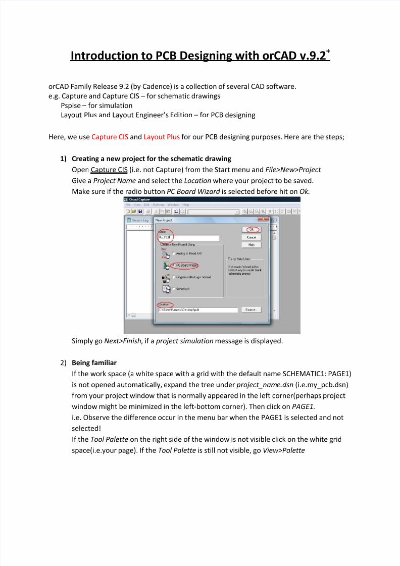
1) Creating a new project for the schematic drawing Open Capture CIS (i.e. not Capture) from the Start menu and File>New>Project
Give a Project Name and select the Location where your project to be saved.
Make sure if the radio button PC Board Wizard is selected before hit on Ok.
Simply go Next>Finish, if a project simulation message is displayed.
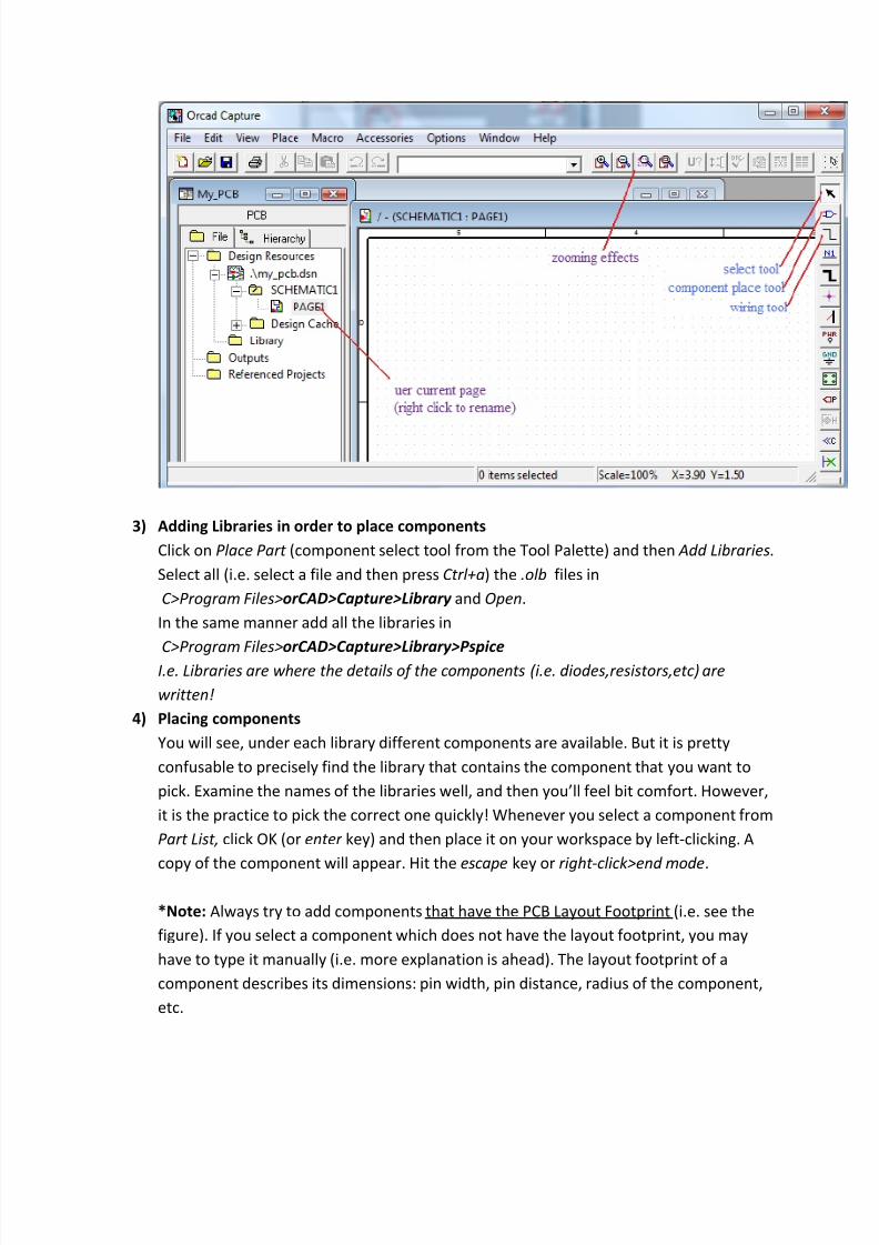
2) Being familiar If the work space (a white space with a grid with the default name SCHEMATIC1: PAGE1)
is not opened automatically, expand the tree under project_name.dsn (i.e.my_pcb.dsn)
from your
project
window
that
is
normally
appeared
in
the
left
corner(perhaps
project
window might be minimized in the left‐bottom corner). Then click on PAGE1.
i.e. Observe the difference occur in the menu bar when the PAGE1 is selected and not
selected!
If the Tool Palette on the right side of the window is not visible click on the white grid
space(i.e.your page). If the Tool Palette is still not visible, go View>Palette
8/13/2019 Introduction to PCB Designing With OrCAD 9
http://slidepdf.com/reader/full/introduction-to-pcb-designing-with-orcad-9 2/9
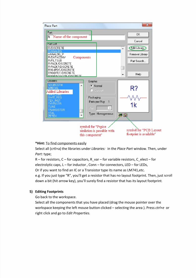
3) Adding Libraries in order to place components Click on Place Part (component select tool from the Tool Palette) and then Add Libraries.
Select all (i.e. select a file and then press Ctrl+a) the .olb files in
C>Program Files>orCAD>Capture>Library and Open. In the same manner add all the libraries in
C>Program
Files>orCAD>Capture>Library>Pspice
I.e. Libraries are where the details of the components (i.e. diodes,resistors,etc) are
written!
4) Placing components You will see, under each library different components are available. But it is pretty
confusable to precisely find the library that contains the component that you want to
pick. Examine the names of the libraries well, and then you’ll feel bit comfort. However,
it is the practice to pick the correct one quickly! Whenever you select a component from
Part List, click OK (or enter key) and then place it on your workspace by left‐clicking. A
copy of the component will appear. Hit the escape key or right ‐click>end mode.
*Note: Always try to add components that have the PCB Layout Footprint (i.e. see the figure). If you select a component which does not have the layout footprint, you may
have to type it manually (i.e. more explanation is ahead). The layout footprint of a
component describes its dimensions: pin width, pin distance, radius of the component,
etc.
8/13/2019 Introduction to PCB Designing With OrCAD 9
http://slidepdf.com/reader/full/introduction-to-pcb-designing-with-orcad-9 3/9
*Hint: To find components easily
Select all (crtl+a) the libraries under Libraries: in the Place Part window. Then, under
Part: type;
R – for resistors, C – for capacitors, R_var – for variable resistors, C_elect – for
electrolytic caps, L – for inductor , Conn – for connectors, LED – for LEDs,
Or if you want to find an IC or a Transistor type its name as LM741,etc.
e.g. If you just type “R”, you’ll get a resistor that has no layout footprint. Then, just scroll
down a bit (hit arrow key), you’ll surely find a resistor that has its layout footprint.
5) Editing Footprints Go
back
to
the
workspace.
Select all the components that you have placed (drag the mouse pointer over the
workspace keeping the left mouse button clicked – selecting the area ). Press ctrl+e or
right click and go to Edit Properties.
8/13/2019 Introduction to PCB Designing With OrCAD 9
http://slidepdf.com/reader/full/introduction-to-pcb-designing-with-orcad-9 4/9
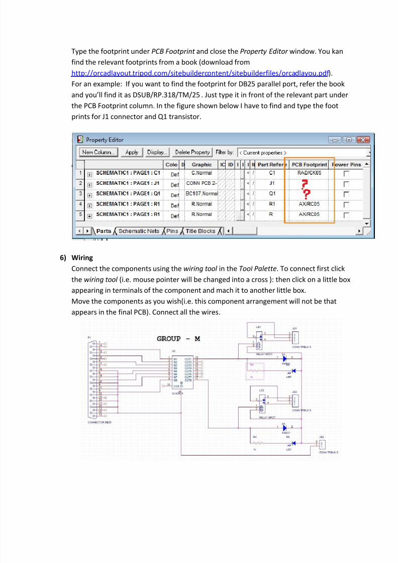
Type the footprint under PCB Footprint and close the Property Editor window. You kan
find the relevant footprints from a book (download from
http://orcadlayout.tripod.com/sitebuildercontent/sitebuilderfiles/orcadlayou.pdf ).
For an example: If you want to find the footprint for DB25 parallel port, refer the book
and
you’ll
find
it
as
DSUB/RP.318/TM/25
.
Just
type
it
in
front
of
the
relevant
part
under
the PCB Footprint column. In the figure shown below I have to find and type the foot
prints for J1 connector and Q1 transistor.
6) Wiring Connect the components using the wiring tool in the Tool Palette. To connect first click
the wiring tool (i.e. mouse pointer will be changed into a cross ): then click on a little box
appearing in terminals of the component and mach it to another little box.
Move the components as you wish(i.e. this component arrangement will not be that
appears in the final PCB). Connect all the wires.

8/13/2019 Introduction to PCB Designing With OrCAD 9
http://slidepdf.com/reader/full/introduction-to-pcb-designing-with-orcad-9 5/9
7) Creating the Netlist
Click on project_name.dsn (i.e. here my_pcb.dsn) . Then go to Tools>Create Netlist and
select the Layout tab.
Under Netlist File: , define the location where the netlist is to be save and click ok . If the
program asks to save the design file, click ok. The netlist will be save with the extension
.MNL. Netlist
is
simply
the
pin
connections
of
your
circuit
diagram
(i.e.
how
they
connect).
8) Creating the layout project Load Layout Plus (i.e. not Layout) from the Start menu. Go to File>New. Select
DEFAULT.TCH file from C:\Program Files\Orcad\Layout_Plus\Data and open. Now select
the netlist file saved in step 7. Thesreafter select the lacation where you want to save
your PCB layout. The PCB layout will be saved as a .MAX file.
Inactivating (from the button) online DRC would be preferable as we do not bother
about PCB design rules. If DRC is not turned off, placing components and routing will,
perhaps give errors.

8/13/2019 Introduction to PCB Designing With OrCAD 9
http://slidepdf.com/reader/full/introduction-to-pcb-designing-with-orcad-9 6/9
8/13/2019 Introduction to PCB Designing With OrCAD 9
http://slidepdf.com/reader/full/introduction-to-pcb-designing-with-orcad-9 7/9
Go to Auto>Place>Board in order to place the components inside the board (i.e. This can be done manually as well). Then move the components using the component tool. You
should place the components in such a manner that it is possible to route and an
arranged manner.
Then go to Tools>Layer>Select from Spreadsheet. Then click on layer type column
header. The entire column will be selected. Then click on the second cell that is already
highlighted(bottom vs. layer type).Then Press ctrl+e (i.e. right click>properties). Click on
the radio button Unused Routing and click ok . Then close the spreadsheet. What really
should happen is making all the unnecessary planes deactivate because here we only
route on the bottom layer.
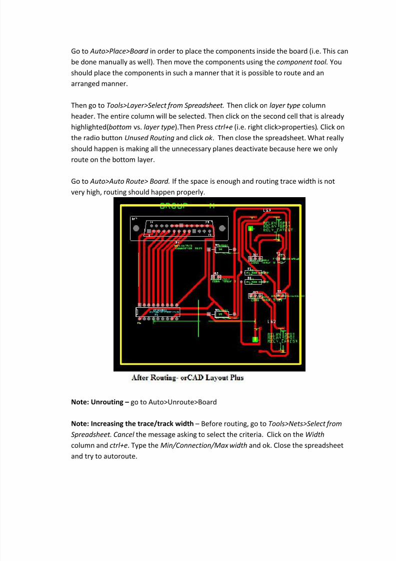
Go to Auto>Auto Route> Board. If the space is enough and routing trace width is not
very high, routing should happen properly.
Note: Unrouting – go to Auto>Unroute>Board Note: Increasing the trace/track width – Before routing, go to Tools>Nets>Select from
Spreadsheet . Cancel the message asking to select the criteria. Click on the Width
column and ctrl+e. Type the Min/Connection/Max width and ok. Close the spreadsheet
and try to autoroute.

8/13/2019 Introduction to PCB Designing With OrCAD 9
http://slidepdf.com/reader/full/introduction-to-pcb-designing-with-orcad-9 8/9

8/13/2019 Introduction to PCB Designing With OrCAD 9
http://slidepdf.com/reader/full/introduction-to-pcb-designing-with-orcad-9 9/9
12) Etching Keep the transparent sheet on a dry and well‐cleaned (clean using an emery paper and
wash well) copper board and heat well (using a domestic iron that is used to iron
clothes) till ink tracks are traced on to the copper board. Keep a typing paper on the
transparent
sheet
for
safety.
It’ll
be
traced
within
5‐
20
minutes.
However
it’s
your
ability
to trace properly from the very first attempt. Draw the untraced places using a
permanent marker.
.
Dissolve Ferric Chloride(FeCl3 (S)) powder in water and put the copper board to etch.
Time will vary from 2 mins – 1 day (typically 15 mins) depending on the concentration of
ferric chloride. To increase the concentration of ferric chloride use slightly hot water
(45oC) and add more powder. But it may harm the traces. After etching is completed
clean the traces using turpentine liquid. Then drill holes using a PCB drill (manual or
electrical).
ferric
chloride
and
a
PCB
drill
could
be
bought
from
shops
where
electronic
components are sold. You are done!
Note: This note is for a beginner of PCB designing. There are many alternatives for most
of the steps. Also ‘ferric chloride method’ kan be considered as the easiest and most
economical method of etching. Safety precautions and disposal of chemicals is also
important. It is all practice to become a good PCB designer! Good Luck!!
Prepared by: (28‐ Dec‐ 09)Ransalu SenanayakeYear 1 Student,{ B.Eng(Hons) Degree in Electronic Engineering – Sheffield Hallam University(UK)},Department of Electronic and Computer Engineering,Sri Lanka Institute of Information Technology, Sri Lanka.
Reference: forum ‐ www.edaboard.com
[Format of the document is NOT in the IEEE standard]