introduction to digital electronics dr. lynn fuller circuit design pmos, nmos, cmos cad, vlsi...
TRANSCRIPT

© March 21, 2017 Dr. Lynn Fuller
Intro to Digital Electronics
Page 1
Rochester Institute of Technology
Microelectronic Engineering
ROCHESTER INSTITUTE OF TECHNOLOGYMICROELECTRONIC ENGINEERING
Introduction to Digital Electronics
Dr. Lynn FullerWebpage: http://people.rit.edu/lffeee
Microelectronic EngineeringRochester Institute of Technology
82 Lomb Memorial DriveRochester, NY 14623-5604
Tel (585) 475-2035Email: [email protected]
Department webpage: http://www.rit.edu/kgcoe/microelectronic/
3-21-2017 IntroDigitalElectronics.ppt
© March 21, 2017 Dr. Lynn Fuller
Intro to Digital Electronics
Page 2
Rochester Institute of Technology
Microelectronic Engineering
ADOBE PRESENTER
This PowerPoint module has been published using Adobe Presenter. Please click on the Notes tab in the left panel to read the instructors comments for each slide. Manually advance the slide by clicking on the play arrow or pressing the page down key.

© March 21, 2017 Dr. Lynn Fuller
Intro to Digital Electronics
Page 3
Rochester Institute of Technology
Microelectronic Engineering
OUTLINE
Brief History of IC IndustryBasic Logic FunctionsLogic (Really Continuous Signals)VTC and Noise MarginTransient CharacteristicsPower DissipationDigital Circuit DesignPMOS, NMOS, CMOSCAD, VLSIStandard Cell DesignSystem on a Chip (SOC)Challenges AheadReferencesHomework

© March 21, 2017 Dr. Lynn Fuller
Intro to Digital Electronics
Page 4
Rochester Institute of Technology
Microelectronic Engineering
SEMICONDUCTOR INDUSTRY
Total $354B in 2015
Industry rankings not including foundries

© March 21, 2017 Dr. Lynn Fuller
Intro to Digital Electronics
Page 5
Rochester Institute of Technology
Microelectronic Engineering
TSMC AND GLOBAL FOUNDRIES
TSMC, Taiwan, $25 Billion in 2015
http://www.tsmc.com/english/default.htm
Global Foundries, $5 Billion in 2015
Malta, New York, Singapore, Dresden, Germany
http://www.globalfoundries.com/
https://www.bing.com/videos/search?q=globalfoundries+malta+ny&&
view=detail&mid=1E207DE7F0772B037C761E207DE7F0772B037
C76&FORM=VRDGAR
2011 Video

© March 21, 2017 Dr. Lynn Fuller
Intro to Digital Electronics
Page 6
Rochester Institute of Technology
Microelectronic Engineering
GLOBAL FOUNDRIES, MALTA, NY
Dr. Tom Caulfield, CEOAnnounced in 20062016, $18 Billion Invested3000 New Employees200 RIT Alumni
Products:45 nm 32 nm SOI22 nm FDSOI14 nm Fin FET7 nm Fin FET in 2017RF SOIMEMSmore

© March 21, 2017 Dr. Lynn Fuller
Intro to Digital Electronics
Page 7
Rochester Institute of Technology
Microelectronic Engineering
JACK KILBY AND ROBERT NOYCE
Nobel Prize in Physics 2001

© March 21, 2017 Dr. Lynn Fuller
Intro to Digital Electronics
Page 8
Rochester Institute of Technology
Microelectronic Engineering
JACK KILBY AT RIT 1986

© March 21, 2017 Dr. Lynn Fuller
Intro to Digital Electronics
Page 9
Rochester Institute of Technology
Microelectronic Engineering
FIRST TRANSISTORS MADE AT RIT 1981
2” n-type siliconwafer
PMOS Transistors
Packaged DeviceAluminum wire bonds
2-17-81
Rob Pearson
Jim Radak
Vt = 12 volts

© March 21, 2017 Dr. Lynn Fuller
Intro to Digital Electronics
Page 10
Rochester Institute of Technology
Microelectronic Engineering
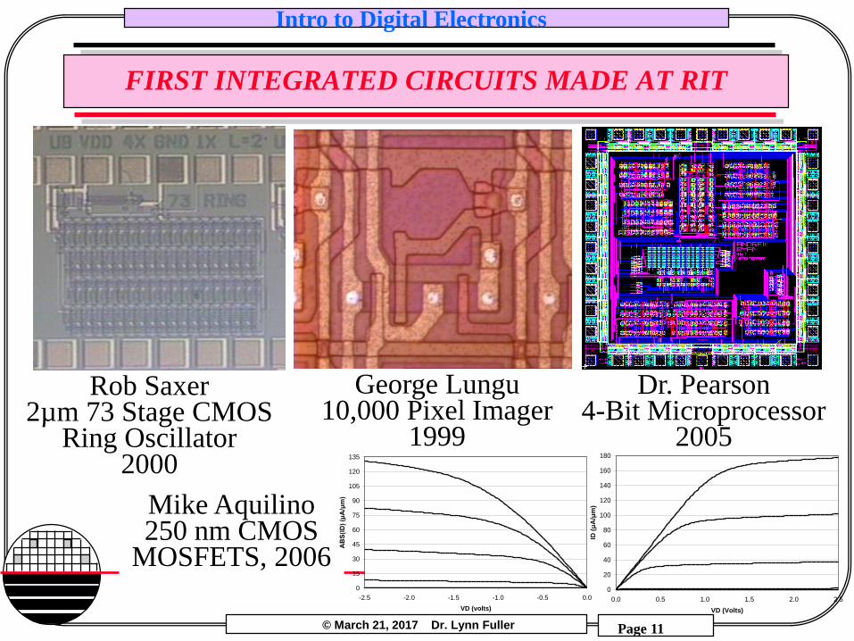
FIRST INTEGRATED CIRCUITS MADE AT RIT
Jonathan Littlehale
All PMOS Op Amp
1985
Jim Pollard Metal
Gate CMOS
1987
Dr. Lane’s
Thin Films Class
NMOS Inverter
1990’s
© March 21, 2017 Dr. Lynn Fuller
Intro to Digital Electronics
Page 11
Rochester Institute of Technology
Microelectronic Engineering
FIRST INTEGRATED CIRCUITS MADE AT RIT
Rob Saxer2µm 73 Stage CMOS
Ring Oscillator 2000
George Lungu10,000 Pixel Imager
1999
Mike Aquilino250 nm CMOS
MOSFETS, 2006
Dr. Pearson4-Bit Microprocessor
2005 ID-VD 0.25 μm NMOS Transistor
0
20
40
60
80
100
120
140
160
180
0.0 0.5 1.0 1.5 2.0 2.5
VD (Volts)
ID (
μA
/μm
)
ID-VD 0.25 μm PMOS Transistor
0
15
30
45
60
75
90
105
120
135
-2.5 -2.0 -1.5 -1.0 -0.5 0.0
VD (volts)
AB
S(I
D)
(μA
/μm
)

© March 21, 2017 Dr. Lynn Fuller
Intro to Digital Electronics
Page 12
Rochester Institute of Technology
Microelectronic Engineering
PROCESS TECHNOLOGY
Process Technology

© March 21, 2017 Dr. Lynn Fuller
Intro to Digital Electronics
Page 13
Rochester Institute of Technology
Microelectronic Engineering
PROCESS SELECTION
It is not necessary to know all process details to do CMOS integrated circuit design. However the process determines important circuit parameters such as supply voltage and maximum frequency of operation. It also determines if devices other than PMOS and NMOS transistors can be realized such as poly-to-poly capacitors and EEPROM transistors. The number of metal interconnect layers is also part of the process definition. Starting wafer type determines if isolated n-wells or p-wells are available.

© March 21, 2017 Dr. Lynn Fuller
Intro to Digital Electronics
Page 14
Rochester Institute of Technology
Microelectronic Engineering
RIT PROCESSES
At RIT we use the Sub-CMOS and ADV-CMOS processes for most designs. In these processes the minimum poly length is 1µm and 0.5µm respectively. We use scalable MOSIS design rules with lambda equal to 0.5µm and 0.25µm. These processes use one layer of poly and two layers of metal.
The examples on the following pages are designs that could be made with either of the above processes. As a result the designs are generous, meaning that larger than minimum dimensions are used. For example l = 0.5µm and minimum poly is 2l which would result in transistor gate length of 1µm but are designed at 2µm for higher yield.
The design approach for digital circuits is to design primitive cells and then use the primitive cells to design basic cells which are then used in the project designs. A layout approach is also used that allows for easy assembly of these cells into more complex cells.

© March 21, 2017 Dr. Lynn Fuller
Intro to Digital Electronics
Page 15
Rochester Institute of Technology
Microelectronic Engineering
RIT SUBµ CMOS
RIT Subµ CMOS150 mm wafersNsub = 1E15 cm-3Nn-well = 3E16 cm-3Xj = 2.5 µmNp-well = 1E16 cm-3Xj = 3.0 µmLOCOSField Ox = 6000 Å Xox = 150 ÅLmin= 1.0 µmLDD/Side Wall Spacers2 Layers Aluminum
L
LongChannelBehavior
3.3 Volt TechnologyVT’s = +/- 0.75 VoltRobust Process (always works)Fully Characterized (SPICE)

© March 21, 2017 Dr. Lynn Fuller
Intro to Digital Electronics
Page 16
Rochester Institute of Technology
Microelectronic Engineering
RIT SUBµ CMOS
Substrate 10 ohm-cm
P-well N-well
5000 ÅField Oxide
NMOSFET PMOSFETN+ Poly
P+ D/SN+ D/S LDD LDD n+ wellcontactp+ well
contact
Channel Stop
© March 21, 2017 Dr. Lynn Fuller
Intro to Digital Electronics
Page 17
Rochester Institute of Technology
Microelectronic Engineering
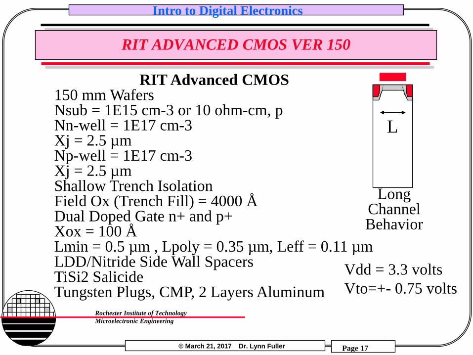
RIT ADVANCED CMOS VER 150
RIT Advanced CMOS150 mm WafersNsub = 1E15 cm-3 or 10 ohm-cm, pNn-well = 1E17 cm-3Xj = 2.5 µmNp-well = 1E17 cm-3Xj = 2.5 µmShallow Trench IsolationField Ox (Trench Fill) = 4000 Å Dual Doped Gate n+ and p+Xox = 100 ÅLmin = 0.5 µm , Lpoly = 0.35 µm, Leff = 0.11 µmLDD/Nitride Side Wall SpacersTiSi2 SalicideTungsten Plugs, CMP, 2 Layers Aluminum
L
LongChannelBehavior
Vdd = 3.3 volts
Vto=+- 0.75 volts

© March 21, 2017 Dr. Lynn Fuller
Intro to Digital Electronics
Page 18
Rochester Institute of Technology
Microelectronic Engineering
RIT ADVANCED CMOS
NMOSFET PMOSFET
N-wellP-well
N+ Poly
P+ D/SN+ D/S
LDDLDD
n+ wellcontact
p+ wellcontact
P+ Poly

© March 21, 2017 Dr. Lynn Fuller
Intro to Digital Electronics
Page 19
Rochester Institute of Technology
Microelectronic Engineering
DIGITAL ELECTRONICS
Digital Electronics

© March 21, 2017 Dr. Lynn Fuller
Intro to Digital Electronics
Page 20
Rochester Institute of Technology
Microelectronic Engineering
DIGITAL INTEGRATED CIRCUITS
BOOLEAN ALGEBRA IS BASED ON TWO DISCRETE LEVELS CALLED LOW OR HIGH (0 OR 1). (from George Boole, 1815-1864)
BOOLEAN ALGEBRA USES FUNCTIONS SUCH AS “INVERT”, “AND”, “OR” TO EVALUATE INPUTS AND GENERATE “OUTPUTS”.
THE TERM “BINARY LOGIC” IS USED TO DESCRIBE DEVICES THAT FOLLOW THE RULES OF BOOLEAN ALGEBRA.
EACH SUB CIRCUIT OR “GATE” SHOULD HAVE ITS INPUTS AND OUTPUTS AT 0 OR 1 (Except Briefly During Switching)
© March 21, 2017 Dr. Lynn Fuller
Intro to Digital Electronics
Page 21
Rochester Institute of Technology
Microelectronic Engineering
BASIC LOGIC FUNCTIONS
INV, NAND NORTruth TablesSum of Products, Product of SumsXOR, XNOR, MUXSequential LogicRS, D, JK, T Flip Flops

© March 21, 2017 Dr. Lynn Fuller
Intro to Digital Electronics
Page 22
Rochester Institute of Technology
Microelectronic Engineering
INVERTER
SYMBOL
RESISTOR
LOAD
TRUTH TABLE
VIN VOUT VOUTVIN
0 1
1 0
VIN
V
SWITCH
R
VIN
+V
VOUT VOUT
R

© March 21, 2017 Dr. Lynn Fuller
Intro to Digital Electronics
Page 23
Rochester Institute of Technology
Microelectronic Engineering
VOLTAGE TRANSFER CURVE
VIN VOUT
+V0
0
+V
ViL
Voh
VoL
Vih
VOUT
VIN
Idd
NML, noise margin low, D0 =ViL-VoLNMH, oise margin high, D1 =VoH-ViH
Slope = Gain
RESISTOR
LOAD
VIN
V
VOUT
R
Vinv

© March 21, 2017 Dr. Lynn Fuller
Intro to Digital Electronics
Page 24
Rochester Institute of Technology
Microelectronic Engineering
LTSPICE - INVERTER VTC – FOR DIFFERENT RL
R=1K
5K10k

© March 21, 2017 Dr. Lynn Fuller
Intro to Digital Electronics
Page 25
Rochester Institute of Technology
Microelectronic Engineering
LTSPICE - INVERTER FOR DIFFERENT NMOS W
10µm
20µm
40µm
W =

© March 21, 2017 Dr. Lynn Fuller
Intro to Digital Electronics
Page 26
Rochester Institute of Technology
Microelectronic Engineering
OTHER INVERTER TYPES - VOUT VS VIN (VTC)
NMOS
ENHANCEMENT
LOAD
VIN
CMOS
+V
VO
SWITCH
VIN
+V
VO
+V
VIN
NMOS
DEPLETION
LOAD
+V
VIN
PMOS
ENHANCEMENT
LOAD
-V
VIN
VO VO
-V+V
+V0
0
+V0
0+V0
0
-V0
0
+V0
0
+V+V +V
VO
© March 21, 2017 Dr. Lynn Fuller
Intro to Digital Electronics
Page 27
Rochester Institute of Technology
Microelectronic Engineering
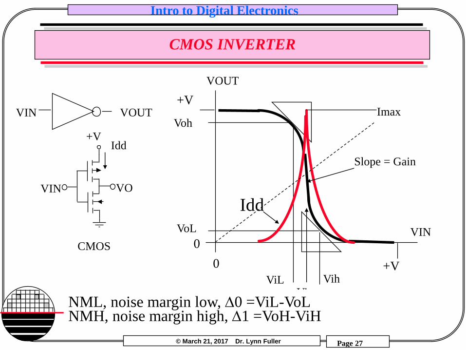
CMOS INVERTER
VIN VOUT
VIN
CMOS
+V
VO
Idd
+V0
0
+V
ViL
Voh
VoL
Vih
Imax
VOUT
VIN
Idd
Slope = Gain
VinvNML, noise margin low, D0 =ViL-VoLNMH, noise margin high, D1 =VoH-ViH

© March 21, 2017 Dr. Lynn Fuller
Intro to Digital Electronics
Page 28
Rochester Institute of Technology
Microelectronic Engineering
LTSPICE – CMOS INVERTER

© March 21, 2017 Dr. Lynn Fuller
Intro to Digital Electronics
Page 29
Rochester Institute of Technology
Microelectronic Engineering
INVERTER PROPERTIES
DC Properties
VTC
Noise Margins
Current, I
Size
Transient Properties
Rise/Fall Time
Gate Delay
Fan Out

© March 21, 2017 Dr. Lynn Fuller
Intro to Digital Electronics
Page 30
Rochester Institute of Technology
Microelectronic Engineering
RISE TIME AND FALL TIME LTSPICE SIMULATION
© March 21, 2017 Dr. Lynn Fuller
Intro to Digital Electronics
Page 31
Rochester Institute of Technology
Microelectronic Engineering
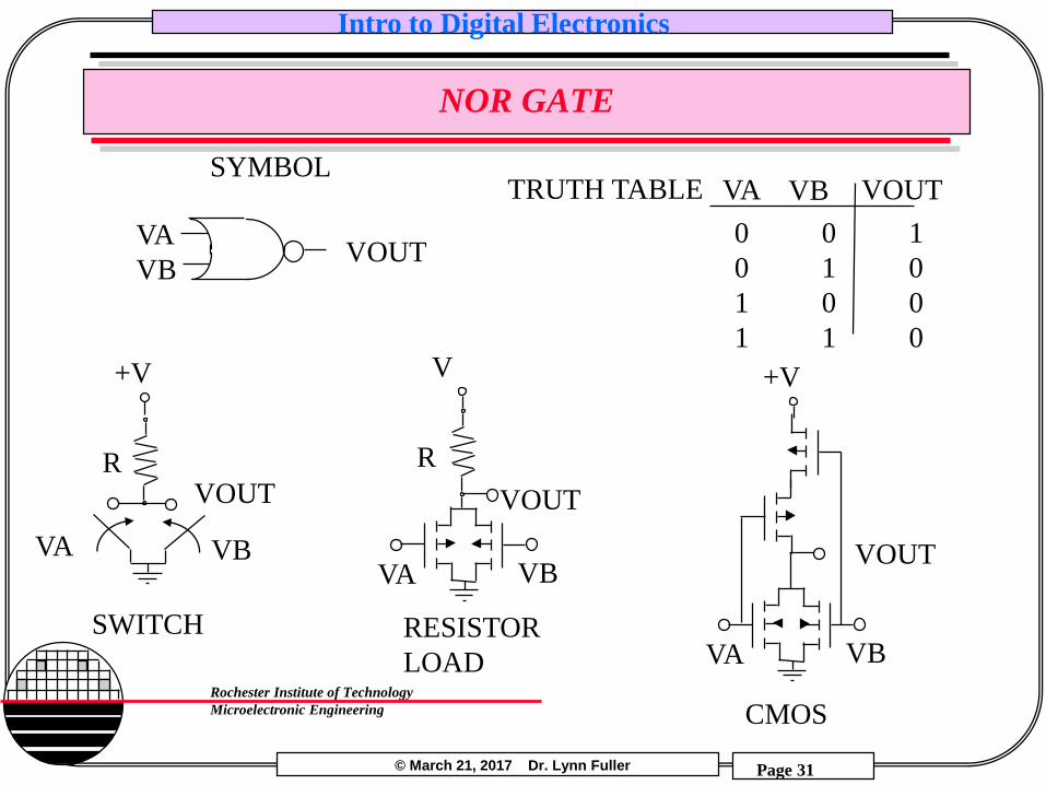
NOR GATE
SYMBOL
RESISTOR
LOAD
TRUTH TABLE VOUTVB
0 0 1
0 1 0
1 0 0
1 1 0V
SWITCH
R
VA
+V
VOUT VOUT
+V
VOUT
VA
VAVOUT
VB
VBVA VB
CMOS
VA VB
R

© March 21, 2017 Dr. Lynn Fuller
Intro to Digital Electronics
Page 32
Rochester Institute of Technology
Microelectronic Engineering
NAND GATE
SYMBOL
RESISTOR
LOAD
TRUTH TABLEVA
VOUT
VOUTVB
0 0 1
0 1 1
1 0 1
1 1 0V
SWITCH
R
VA
+V
VOUT
+V
VA
VB
VB
VOUTVA
VB
CMOS
VOUTVA
VB
R
NAND GATE

© March 21, 2017 Dr. Lynn Fuller
Intro to Digital Electronics
Page 33
Rochester Institute of Technology
Microelectronic Engineering
OTHER LOGIC GATES
VAVOUT
VB
VOUTVB
0 0 0 0
0 0 1 0
0 1 0 0
0 1 1 0
1 0 0 0
1 0 1 0
1 1 0 0
1 1 1 1
VAVOUTVOUTVB
0 0 0
0 1 0
1 0 0
1 1 1
VA VB
0 0 0
0 1 1
1 0 1
1 1 1
VA
VB
VAVOUT
ORAND 3 INPUT OR3 INPUT AND
VC VOUTVBVA
0 0 0 0
0 0 1 1
0 1 0 1
0 1 1 1
1 0 0 1
1 0 1 1
1 1 0 1
1 1 1 1
VC
VAVAVB VBVC VC
VOUT VOUT
© March 21, 2017 Dr. Lynn Fuller
Intro to Digital Electronics
Page 34
Rochester Institute of Technology
Microelectronic Engineering
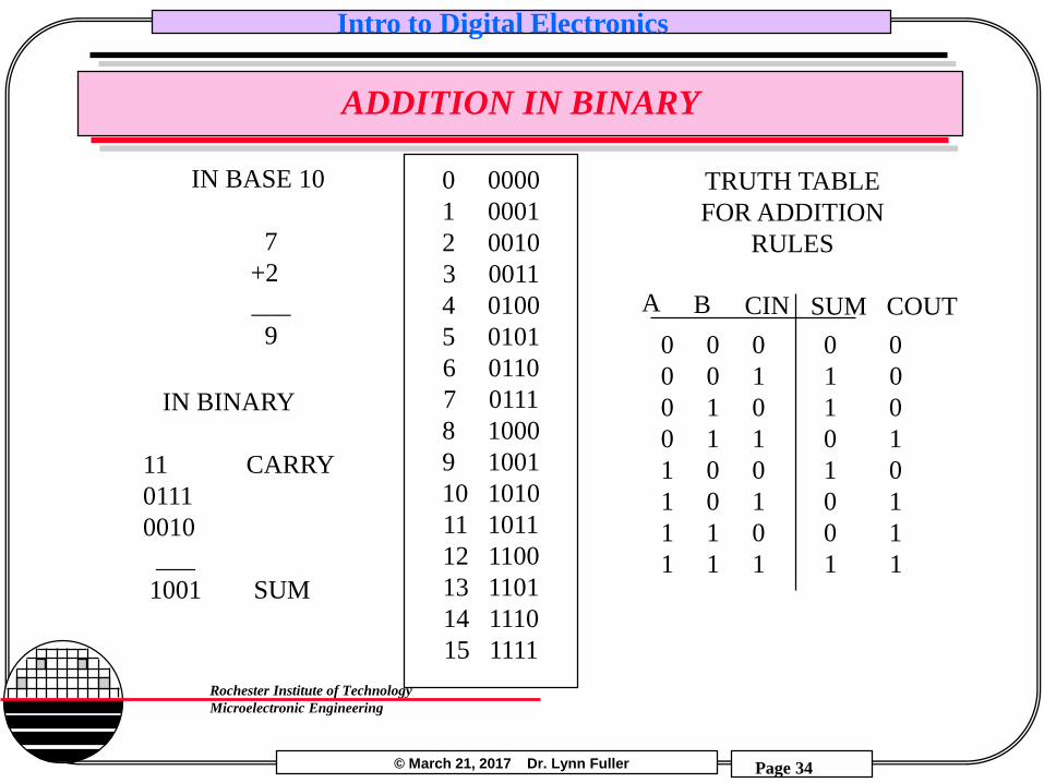
ADDITION IN BINARY
IN BASE 10
7
+2
___
9
IN BINARY
11 CARRY
0111
0010
___
1001 SUM
0 0000
1 0001
2 0010
3 0011
4 0100
5 0101
6 0110
7 0111
8 1000
9 1001
10 1010
11 1011
12 1100
13 1101
14 1110
15 1111
SUM COUTBA
0 0 0 0 0
0 0 1 1 0
0 1 0 1 0
0 1 1 0 1
1 0 0 1 0
1 0 1 0 1
1 1 0 0 1
1 1 1 1 1
CIN
TRUTH TABLE
FOR ADDITION
RULES

© March 21, 2017 Dr. Lynn Fuller
Intro to Digital Electronics
Page 35
Rochester Institute of Technology
Microelectronic Engineering
AND-OR CIRCUIT REALIZATION OF SUM
SUM COUTBA
0 0 0 0 0
0 0 1 1 0
0 1 0 1 0
0 1 1 0 1
1 0 0 1 0
1 0 1 0 1
1 1 0 0 1
1 1 1 1 1
CIN
TRUTH TABLE
FOR ADDITION
RULES
A
SUM
CinB

© March 21, 2017 Dr. Lynn Fuller
Intro to Digital Electronics
Page 36
Rochester Institute of Technology
Microelectronic Engineering
CIRCUIT REALIZATION OF CARRY OUT (COUT)
SUM COUTBA
0 0 0 0 0
0 0 1 1 0
0 1 0 1 0
0 1 1 0 1
1 0 0 1 0
1 0 1 0 1
1 1 0 0 1
1 1 1 1 1
CIN
TRUTH TABLE
FOR ADDITION
RULES
A
COUT
CinB
© March 21, 2017 Dr. Lynn Fuller
Intro to Digital Electronics
Page 37
Rochester Institute of Technology
Microelectronic Engineering
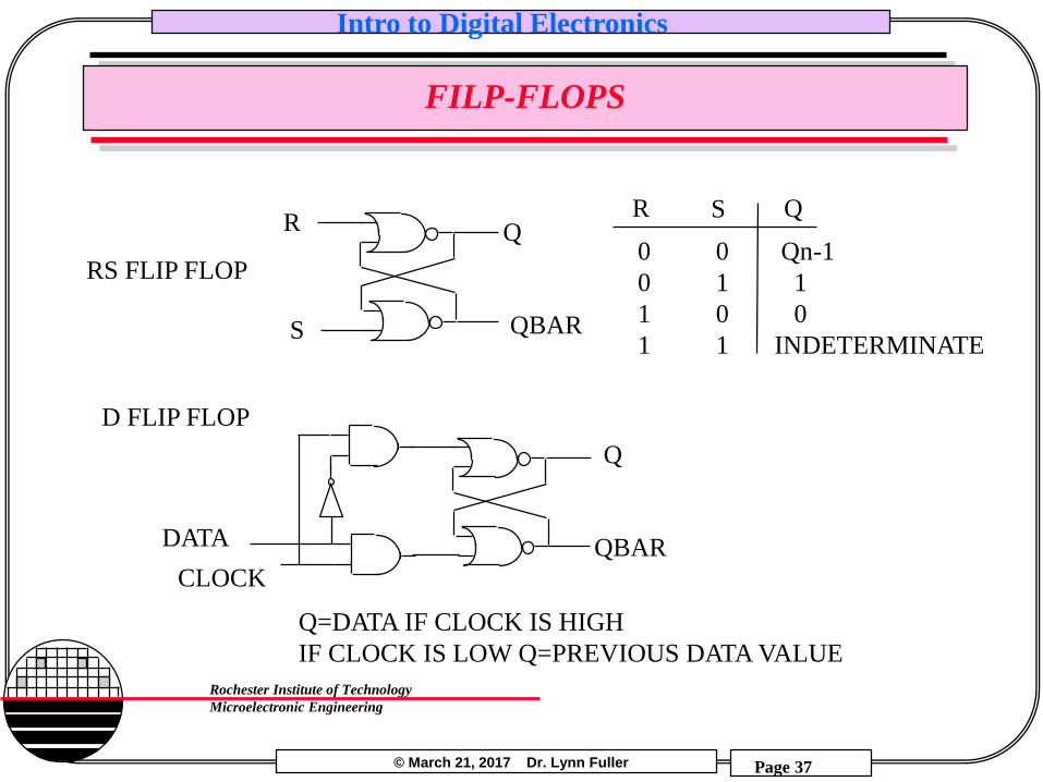
FILP-FLOPS
RS FLIP FLOP
QBARS
R Q
D FLIP FLOP
Q
QBARDATA
QS
0 0 Qn-1
0 1 1
1 0 0
1 1 INDETERMINATE
R
Q=DATA IF CLOCK IS HIGH
IF CLOCK IS LOW Q=PREVIOUS DATA VALUE
CLOCK

© March 21, 2017 Dr. Lynn Fuller
Intro to Digital Electronics
Page 38
Rochester Institute of Technology
Microelectronic Engineering
MASTER-SLAVE D FLIP FLOP
DATA
CLOCK
Q
QBAR
NEGATED INPUT NOR IS EQUAL TO AND
B
0 0 1
0 1 1
1 0 0
1 1 0
A OUT
1 1 0
0 1 0
1 1 0
0 0 1
BA OUT
B
=OUT
B
AA
A
B

© March 21, 2017 Dr. Lynn Fuller
Intro to Digital Electronics
Page 39
Rochester Institute of Technology
Microelectronic Engineering
ALL NOR MASTER SLAVE D FLIP FLOP
DATA
CLOCK
Q
DATA
CLOCK
Q

© March 21, 2017 Dr. Lynn Fuller
Intro to Digital Electronics
Page 40
Rochester Institute of Technology
Microelectronic Engineering
EQUAVILANT REALIZATIONS
AND-OR realizations are easily derived from truth table description of a circuits performance. Replacing the AND and OR gates with all NOR gates is equivalent. Replacing the AND and OR gates with all NAND gates is equivalent.

© March 21, 2017 Dr. Lynn Fuller
Intro to Digital Electronics
Page 41
Rochester Institute of Technology
Microelectronic Engineering
CIRCUIT REALIZATION FOR XOR
A
COUT
B
VOUTVB
0 0 0
0 1 1
1 0 1
1 1 0
VAExclusive OR
XOR
A
COUT
B
COUT
BA

© March 21, 2017 Dr. Lynn Fuller
Intro to Digital Electronics
Page 42
Rochester Institute of Technology
Microelectronic Engineering
VLSI
VLSI
Very Large Scale Integration

© March 21, 2017 Dr. Lynn Fuller
Intro to Digital Electronics
Page 43
Rochester Institute of Technology
Microelectronic Engineering
INTRODUCTION
VLSI is an acronym for Very Large Scale Integration. This includes Integrated circuits with greater than tens of thousands of transistors including multi-million or even billions of transistors.
VLSI Design refers to methodologies and computer software tools for designing digital circuits with huge numbers of transistors. Some of theses methodologies and tools can also be applied to analog circuit design.
Software tools include schematic capture, SPICE analog simulation, switch level digital simulation, layout editors, layout versus schematic checking, design rule checking (DRC), auto place and routing and many more.

© March 21, 2017 Dr. Lynn Fuller
Intro to Digital Electronics
Page 44
Rochester Institute of Technology
Microelectronic Engineering
VLSI DESIGN
Computer software is used to check the layout, compare the layout to the schematic and make it possible to design circuits with millions of transistors with no errors.

© March 21, 2017 Dr. Lynn Fuller
Intro to Digital Electronics
Page 45
Rochester Institute of Technology
Microelectronic Engineering
VLSI DESIGN METHODOLOGIES
Full Custom DesignDirect control of layout and device parametersLonger design timeHigh performance
fast, low power, dense
Standard Cell DesignEasy to implementMedium performanceLimited cell library selections
Gate Array or Programmable Logic Array Design
Fastest design turn around

© March 21, 2017 Dr. Lynn Fuller
Intro to Digital Electronics
Page 46
Rochester Institute of Technology
Microelectronic Engineering
LAYOUT
Layout Design Rules
© March 21, 2017 Dr. Lynn Fuller
Intro to Digital Electronics
Page 47
Rochester Institute of Technology
Microelectronic Engineering
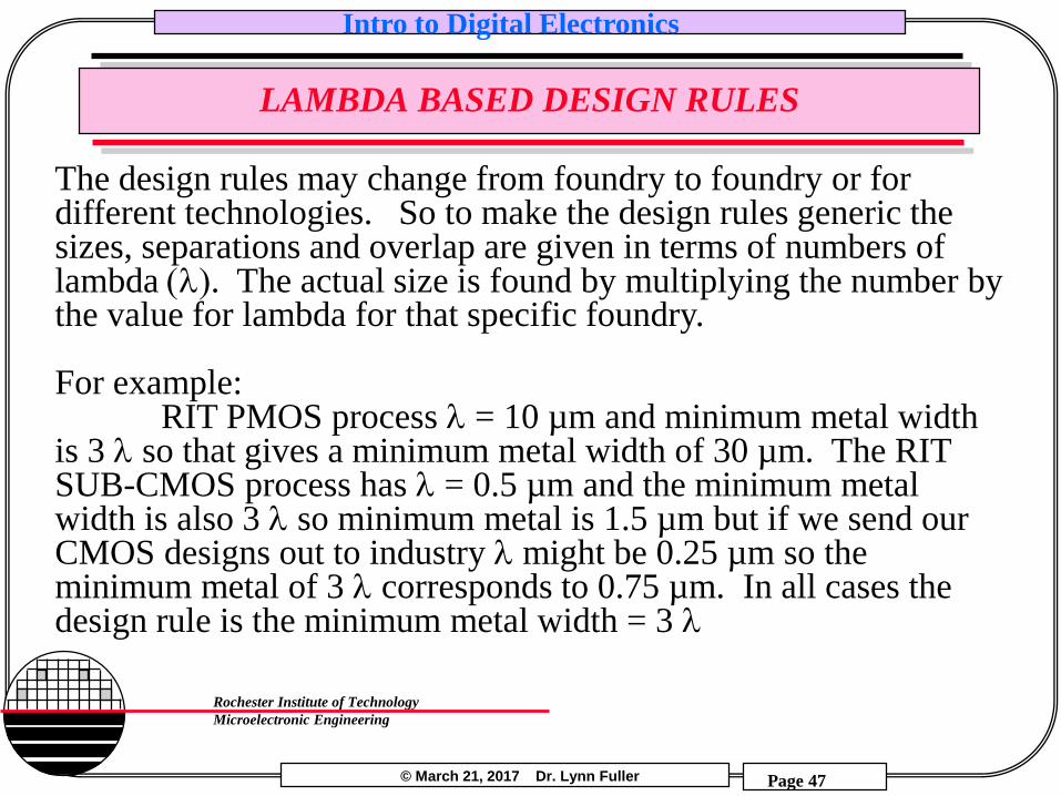
LAMBDA BASED DESIGN RULES
The design rules may change from foundry to foundry or for different technologies. So to make the design rules generic the sizes, separations and overlap are given in terms of numbers of lambda (l). The actual size is found by multiplying the number by the value for lambda for that specific foundry.
For example:RIT PMOS process l = 10 µm and minimum metal width
is 3 l so that gives a minimum metal width of 30 µm. The RIT SUB-CMOS process has l = 0.5 µm and the minimum metal width is also 3 l so minimum metal is 1.5 µm but if we send our CMOS designs out to industry l might be 0.25 µm so the minimum metal of 3 l corresponds to 0.75 µm. In all cases the design rule is the minimum metal width = 3 l

© March 21, 2017 Dr. Lynn Fuller
Intro to Digital Electronics
Page 48
Rochester Institute of Technology
Microelectronic Engineering
DESIGN RULES
We will use a modified version of the MOSIS TSMC 0.35 2P 4M design rules. Eventually we hope to be compatible with MOSIS but new process technology needs to be developed at RIT to do that (PECVD Tungsten, 4 layer metal). We use one layer of poly and two layers of metal. We will use the same design layer numbers with additional layers as defined on the following pages for manufacturing/maskmaking enhancements. Many of the designs will use minimum drawn poly gate lengths of 2µm where circuit architecture is the main purpose of the design. Minimum size devices (Drawn Poly = 0.5µm, etc.) are included to develop manufacturing process technology. These transistors (0.5µm drawn) yield 0.35µm Leff and are equivalent to the TSMC 0.35µm transistors.

© March 21, 2017 Dr. Lynn Fuller
Intro to Digital Electronics
Page 49
Rochester Institute of Technology
Microelectronic Engineering
LAMBDA, Lmin, Ldrawn, Lmask, Lpoly, Lint, Leff, L
Leff
L
Source at 0 V
Drain at 3.3V
Gate
Ldrawn
Lmask
Lpoly
Lmin = min drawn poly length, 2l
Lresist after photo (resist trimming??)
Lmask = ? Depends on +/-bias
Lpoly after poly reoxidation
Internal Channel Length, Lint =distance between junctions, including under diffusion
Effective Channel Length, Leff = distance between space charge layers,Vd = Vs= 0
Channel Length, L, = distance between space charge layers, when Vd= what it is
Extracted Channel Length Parameters = anything that makes the fit good (not real)
Lint
0.50µm
1.00µm x 5
0.50µm
0.35µm
0.30µm
0.20µm
0.11µm
Lpoly after poly etch 0.40µm
Ldrawn = what was drawn
Lambda = design rule parameter, l, ie 0.25µm

© March 21, 2017 Dr. Lynn Fuller
Intro to Digital Electronics
Page 50
Rochester Institute of Technology
Microelectronic Engineering
MOSIS TSMC 0.35 2POLY 4 METAL PROCESS
http://www.mosis.com/Technical/Designrules/scmos/scmos-main.html#tech-codes

© March 21, 2017 Dr. Lynn Fuller
Intro to Digital Electronics
Page 51
Rochester Institute of Technology
Microelectronic Engineering
MOSIS TSMC 0.35 2-POLY 4-METAL LAYERS
MASK LAYER NAME
MENTOR NAME
GDS #
COMMENT
N WELL N_well.i 42
ACTIVE Active.i 43
POLY Poly.i 46
N PLUS N_plus_select.i 45
P PLUS P_plus_select.i 44
CONTACT Contact.i 25 Active_contact.i 48
poly_contact.i 47
METAL1 Metal1.i 49
VIA Via.i 50
METAL2 Metal2.i 51
VIA2 Via2.i 61 Under Bump Metal
METAL3 Metal3.i 62 Solder Bump
These are the main design layers up through metal two

© March 21, 2017 Dr. Lynn Fuller
Intro to Digital Electronics
Page 52
Rochester Institute of Technology
Microelectronic Engineering
MOSIS LAMBDA BASED DESIGN RULES
10 6
9
Well
Same
Potential
Diff
Potential
3
3
3
Active in p-well
n+p+
n+
well edge
n-Substrate
(Outside well)
5
Poly
2
2
3
2
1
Poly
Poly
Active
1
p select
active
2
3 contact to poly
2
2
2
2
metal
2
1
2
33
1
1
If l = 1 µm then contact is2 µm x 2 µm
p+
5
n+
3
http://www.mosis.com/design/rules/
© March 21, 2017 Dr. Lynn Fuller
Intro to Digital Electronics
Page 53
Rochester Institute of Technology
Microelectronic Engineering
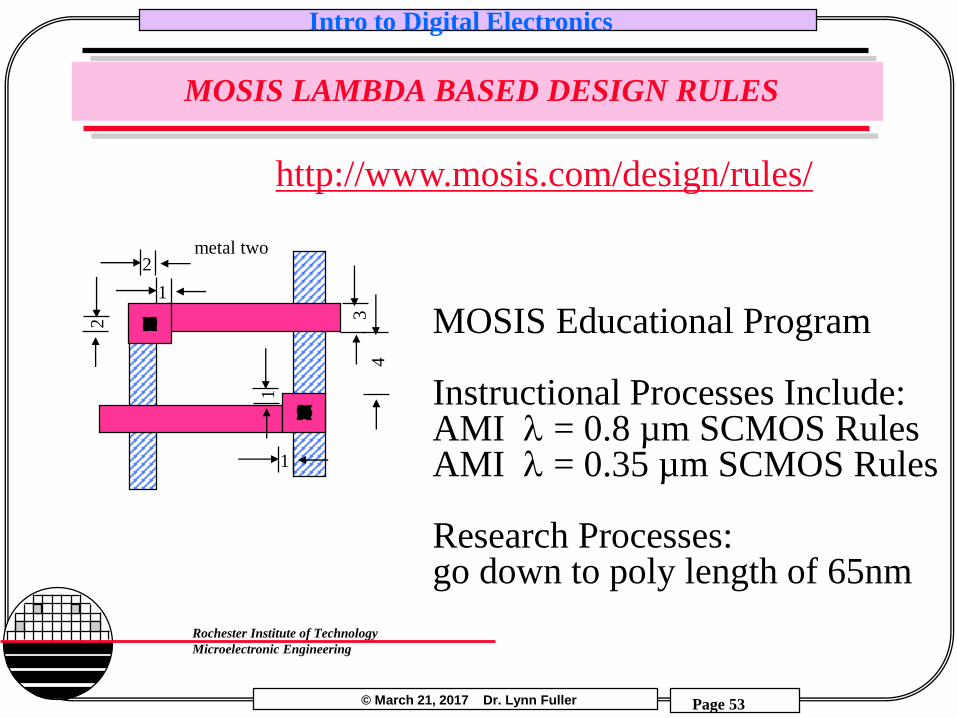
MOSIS LAMBDA BASED DESIGN RULES
metal two2
1
2
43
1
1
http://www.mosis.com/design/rules/
MOSIS Educational Program
Instructional Processes Include: AMI l = 0.8 µm SCMOS RulesAMI l = 0.35 µm SCMOS Rules
Research Processes:go down to poly length of 65nm

© March 21, 2017 Dr. Lynn Fuller
Intro to Digital Electronics
Page 54
Rochester Institute of Technology
Microelectronic Engineering
MOSIS REQUIREMENTS
MOSIS requires that projects have successfully passed LVS (Layout Versus Schematic) and DRC (Design Rule Checking). The MENTOR tools for LVS and DRC (as they are set up at RIT) require separate N-select and P-select levels in order to know an NMOS transistor from a PMOS transistor. Although either an N-well, P-well or both will work for a twin well process, we have set up our DRC to look for N-well. (Also since we use a p-type starting wafer we can not have isolated p-wells but we can have isolated n-wells, thus drawing separate n-wells can be useful for some circuit designs.)
http://www.mosis.com

© March 21, 2017 Dr. Lynn Fuller
Intro to Digital Electronics
Page 55
Rochester Institute of Technology
Microelectronic Engineering
LAYOUT
Digital Circuit Layout
© March 21, 2017 Dr. Lynn Fuller
Intro to Digital Electronics
Page 56
Rochester Institute of Technology
Microelectronic Engineering
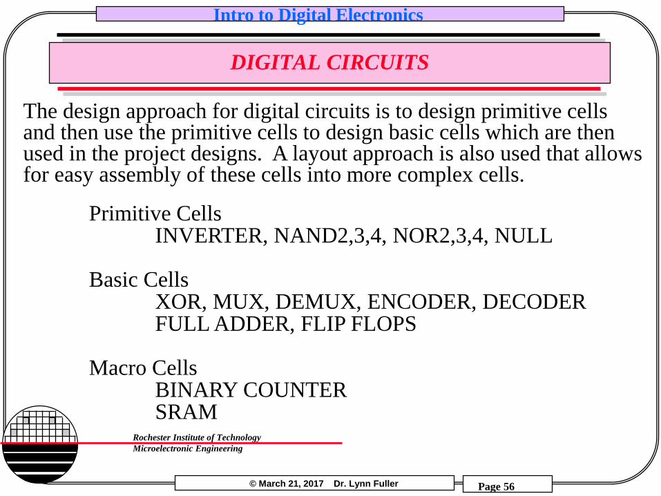
DIGITAL CIRCUITS
Primitive CellsINVERTER, NAND2,3,4, NOR2,3,4, NULL
Basic CellsXOR, MUX, DEMUX, ENCODER, DECODERFULL ADDER, FLIP FLOPS
Macro CellsBINARY COUNTERSRAM
The design approach for digital circuits is to design primitive cells and then use the primitive cells to design basic cells which are then used in the project designs. A layout approach is also used that allows for easy assembly of these cells into more complex cells.
© March 21, 2017 Dr. Lynn Fuller
Intro to Digital Electronics
Page 57
Rochester Institute of Technology
Microelectronic Engineering
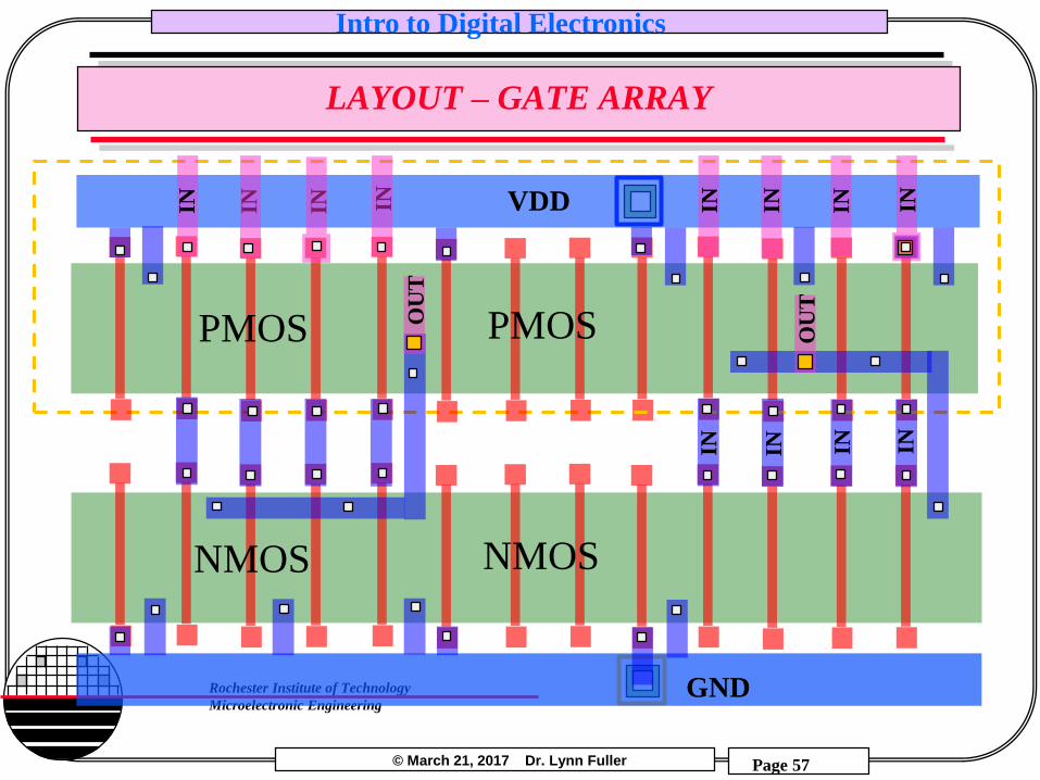
LAYOUT – GATE ARRAY
GND
INININ
NMOS
PMOS
IN
OU
T
VDDININ
IN
IN
OU
T
IN
NMOS
PMOS
INININ
© March 21, 2017 Dr. Lynn Fuller
Intro to Digital Electronics
Page 58
Rochester Institute of Technology
Microelectronic Engineering
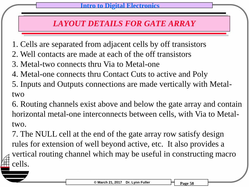
LAYOUT DETAILS FOR GATE ARRAY
1. Cells are separated from adjacent cells by off transistors
2. Well contacts are made at each of the off transistors
3. Metal-two connects thru Via to Metal-one
4. Metal-one connects thru Contact Cuts to active and Poly
5. Inputs and Outputs connections are made vertically with Metal-
two
6. Routing channels exist above and below the gate array and contain
horizontal metal-one interconnects between cells, with Via to Metal-
two.
7. The NULL cell at the end of the gate array row satisfy design
rules for extension of well beyond active, etc. It also provides a
vertical routing channel which may be useful in constructing macro
cells.

© March 21, 2017 Dr. Lynn Fuller
Intro to Digital Electronics
Page 59
Rochester Institute of Technology
Microelectronic Engineering
INVERTER
Vin Vout
Vin
CMOS
+V
Vout
Idd
TRUTH TABLE
VOUTVIN
0 1
1 0
PMOS
NMOS
W = 40 µm
Ldrawn = 2.5µm
Lpoly = 1.0µm
Leff = 0.35 µm

© March 21, 2017 Dr. Lynn Fuller
Intro to Digital Electronics
Page 60
Rochester Institute of Technology
Microelectronic Engineering
INVERTER
W = 40 µmLdrawn = 2.5µmLpoly = 1.0µmLeff = 0.35 µm

© March 21, 2017 Dr. Lynn Fuller
Intro to Digital Electronics
Page 61
Rochester Institute of Technology
Microelectronic Engineering
LAYOUT OF SOME PRIMITIVE CELLS
© March 21, 2017 Dr. Lynn Fuller
Intro to Digital Electronics
Page 62
Rochester Institute of Technology
Microelectronic Engineering
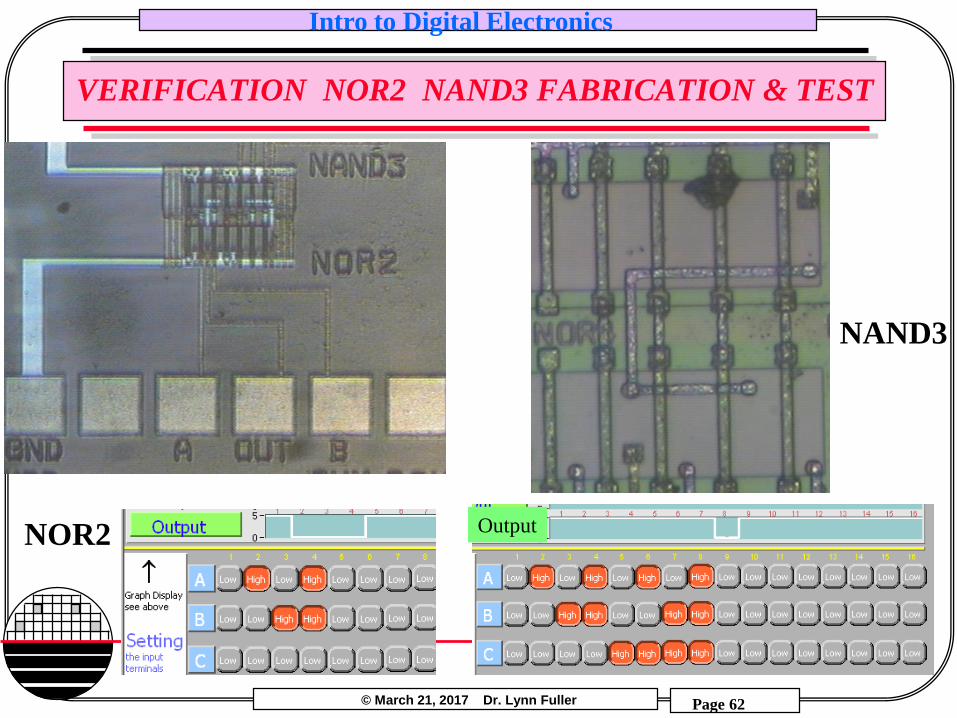
VERIFICATION NOR2 NAND3 FABRICATION & TEST
NOR2 Output
NAND3

© March 21, 2017 Dr. Lynn Fuller
Intro to Digital Electronics
Page 63
Rochester Institute of Technology
Microelectronic Engineering
BASIC DIGITAL CELLS WITH PADS
Multiplexer XOR Full Adder Encoder Decoder Demux
Edge Triggered D FF
Decoder
JK FF

© March 21, 2017 Dr. Lynn Fuller
Intro to Digital Electronics
Page 64
Rochester Institute of Technology
Microelectronic Engineering
4 TO 1 MULTIPLEXER
I0
I1
I2
I3
Q
A
B

© March 21, 2017 Dr. Lynn Fuller
Intro to Digital Electronics
Page 65
Rochester Institute of Technology
Microelectronic Engineering
BASIC CELL XOR
Port out
Input A
XOR
Input B
Port in
Port in
XOR = A’B+AB’
A’
B
B’
A
A’B
AB’
XOR

© March 21, 2017 Dr. Lynn Fuller
Intro to Digital Electronics
Page 66
Rochester Institute of Technology
Microelectronic Engineering
FULL ADDER
A
SUM
CinB

© March 21, 2017 Dr. Lynn Fuller
Intro to Digital Electronics
Page 67
Rochester Institute of Technology
Microelectronic Engineering
1 TO 4 DEMULTIPLEXER
A
B
I
Q0
Q1
Q2
Q3
Correct

© March 21, 2017 Dr. Lynn Fuller
Intro to Digital Electronics
Page 68
Rochester Institute of Technology
Microelectronic Engineering
DECODER
Q0
Q1
Q2
Q3
A
B
Correct

© March 21, 2017 Dr. Lynn Fuller
Intro to Digital Electronics
Page 69
Rochester Institute of Technology
Microelectronic Engineering
ENCODER
Q0 Q1
0 0
0 1
1 0
1 1
A B C D
1 0 0 0
0 1 0 0
0 0 1 0
0 0 0 1
Q0Q1Q2
Qn
Coded
Output
Lines
Digital Encoder
512 inputs can be coded into 9 lines
which is a more dramatic benefit
AB
CD
Q1
Q2No Connection

© March 21, 2017 Dr. Lynn Fuller
Intro to Digital Electronics
Page 70
Rochester Institute of Technology
Microelectronic Engineering
EDGE TRIGGERED D TYPE FLIP FLOP
© March 21, 2017 Dr. Lynn Fuller
Intro to Digital Electronics
Page 71
Rochester Institute of Technology
Microelectronic Engineering
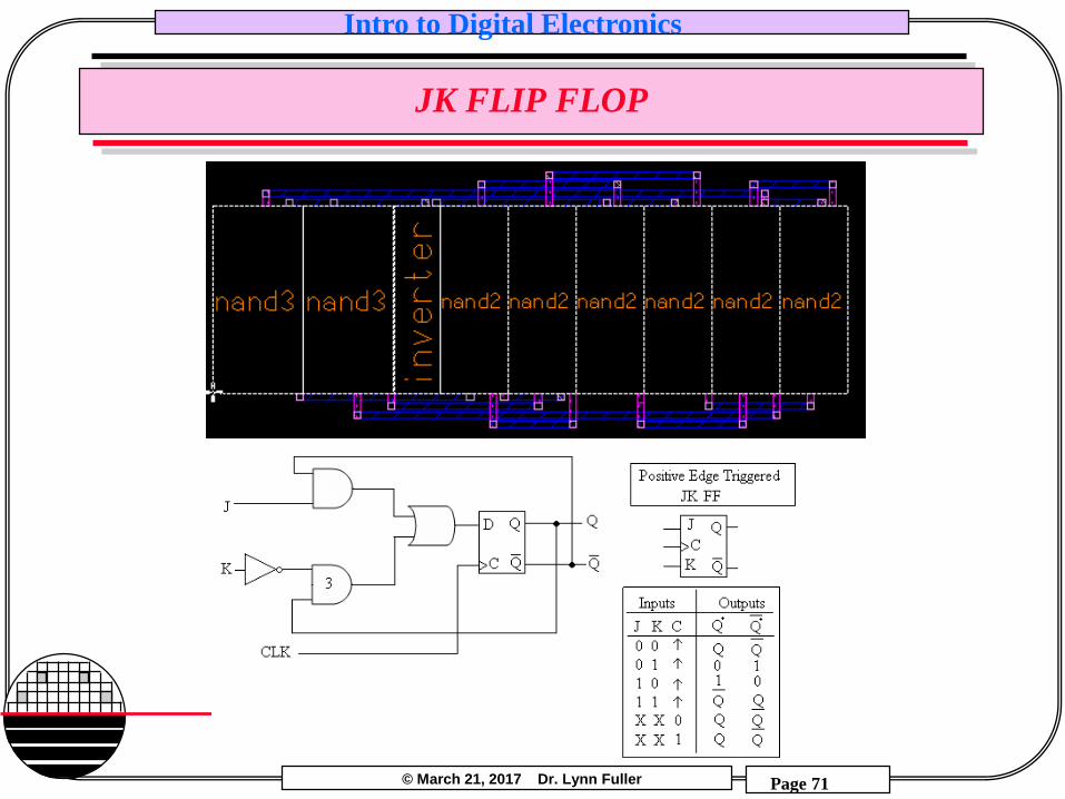
JK FLIP FLOP

© March 21, 2017 Dr. Lynn Fuller
Intro to Digital Electronics
Page 72
Rochester Institute of Technology
Microelectronic Engineering
T-TYPE FILP-FLOP
TOGGEL FLIP FLOP
Q
QBAR
Q: Toggles High and Low with Each Input
QQn-1
0 0 0
0 1 1
1 0 1
1 1 0
T
T
© March 21, 2017 Dr. Lynn Fuller
Intro to Digital Electronics
Page 73
Rochester Institute of Technology
Microelectronic Engineering
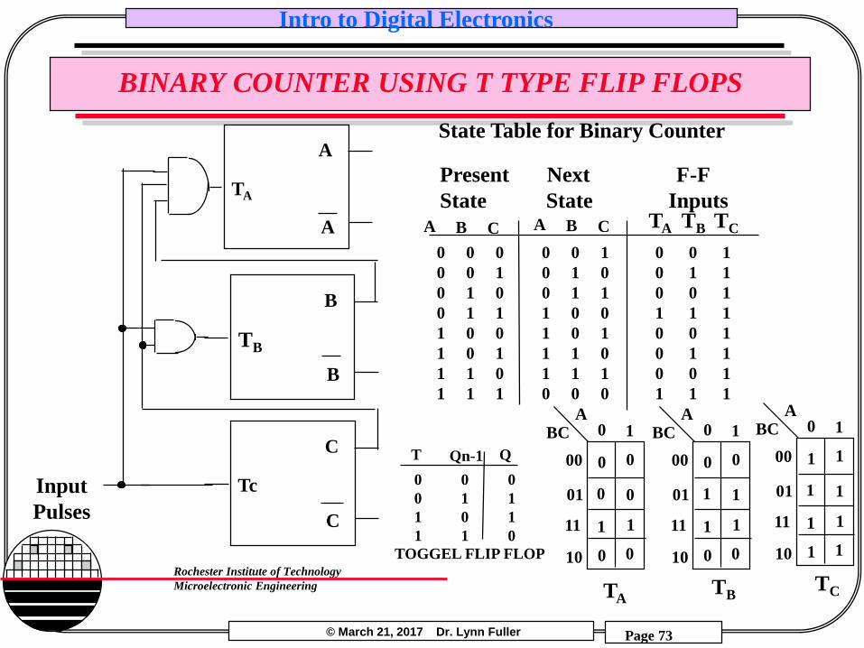
BINARY COUNTER USING T TYPE FLIP FLOPS
TOGGEL FLIP FLOP
QQn-1
0 0 0
0 1 1
1 0 1
1 1 0
T
BA
0 0 0 0 0 1 0 0 1
0 0 1 0 1 0 0 1 1
0 1 0 0 1 1 0 0 1
0 1 1 1 0 0 1 1 1
1 0 0 1 0 1 0 0 1
1 0 1 1 1 0 0 1 1
1 1 0 1 1 1 0 0 1
1 1 1 0 0 0 1 1 1
C
State Table for Binary Counter
Present Next F-F
State State InputsBA C TA TB TC
ABC 0 1
00
01
11
10
0
0
0
1 1
0
00
Input
Pulses
TA
ABC 0 1
00
01
11
10
0
1
0
1 1
1
00
TB
ABC 0 1
00
01
11
10
1
1
1
1 1
1
11
TC
A
A
TA
B
B
TB
C
C
Tc

© March 21, 2017 Dr. Lynn Fuller
Intro to Digital Electronics
Page 74
Rochester Institute of Technology
Microelectronic Engineering
3-BIT BINARY COUNTER WITH D FLIP FLOPS

© March 21, 2017 Dr. Lynn Fuller
Intro to Digital Electronics
Page 75
Rochester Institute of Technology
Microelectronic Engineering
MACROCELLS
Binary Counter
SRAM

© March 21, 2017 Dr. Lynn Fuller
Intro to Digital Electronics
Page 76
Rochester Institute of Technology
Microelectronic Engineering
3-BIT BINARY COUNTER/SHIFT REGISTER
Binary CounterSerial OutputAsynchronous ResetCount Up EnableShift Out Clock InputCount Up Clock InputStart Bit and Stop Bit

© March 21, 2017 Dr. Lynn Fuller
Intro to Digital Electronics
Page 77
Rochester Institute of Technology
Microelectronic Engineering
ADDITIONAL CIRCUITRY TO RESET, SHIFT, COUNT
© March 21, 2017 Dr. Lynn Fuller
Intro to Digital Electronics
Page 78
Rochester Institute of Technology
Microelectronic Engineering
MASKMAKING
Maskmaking

© March 21, 2017 Dr. Lynn Fuller
Intro to Digital Electronics
Page 79
Rochester Institute of Technology
Microelectronic Engineering
MASK PROCESS FLOW
GDSII CATS
Computer Aided
Transcription Software
MEBES
FileMEBES
Job
Coat
PlateExposeInspectEtch Cr
Inspect
Develop
Clean
IC Graph by Mentor
Graphics
CAD
Data Prep
Ship out
Maskmaking
This process can take weeks and cost between $1000 and
$20,000 for each mask depending on the design complexity.

© March 21, 2017 Dr. Lynn Fuller
Intro to Digital Electronics
Page 80
Rochester Institute of Technology
Microelectronic Engineering
OTHER MASKMAKING FEATURES
Fiducial Marks-marks on the edge of the mask used to
align the mask to the stepper
Barcodes
Titles
Alignment Keys- marks on the wafer from a previous
level used for wafer alignment
CD Resolution Targets- lines and spaces
Overlay Verniers- structures that allow measurement
of x and y overlay accuracy
Tiling
Optical Proximity Correction (OPC)

© March 21, 2017 Dr. Lynn Fuller
Intro to Digital Electronics
Page 81
Rochester Institute of Technology
Microelectronic Engineering
MEBES - Manufacturing Electron Beam Exposure System

© March 21, 2017 Dr. Lynn Fuller
Intro to Digital Electronics
Page 82
Rochester Institute of Technology
Microelectronic Engineering
ASML RETICLE
Chrome SideMirrored 90°
Chip Bottom at Bottom
Non Chrome SideAs loaded into Reticle Pod, Chrome Down, Reticle Pre-Alignment Stars Sticking out
of Pod

© March 21, 2017 Dr. Lynn Fuller
Intro to Digital Electronics
Page 83
Rochester Institute of Technology
Microelectronic Engineering
ASML 5500/200
NA = 0.48 to 0.60 variable= 0.35 to 0.85 variable
With Variable Kohler, orVariable Annular illuminationResolution = K1 l/NA
= ~ 0.35µm for NA=0.6, =0.85
Depth of Focus = k2 l/(NA)2
= > 1.0 µm for NA = 0.6i-Line Stepper l = 365 nm
22 x 27 mm Field Size
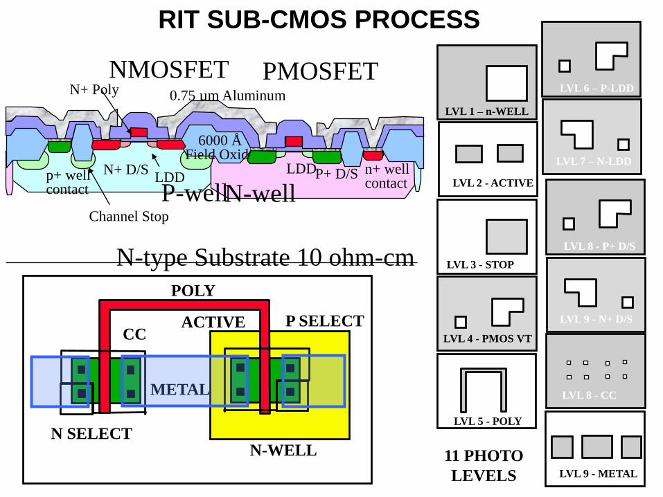
RIT SUB-CMOS PROCESS
11 PHOTO
LEVELS
POLY
METAL
N-WELL
P SELECTCC
ACTIVE
0.75 µm Aluminum
N-type Substrate 10 ohm-cm
P-wellN-well
6000 ÅField Oxide
NMOSFET PMOSFETN+ Poly
Channel Stop
P+ D/SN+ D/SLDD
LDD n+ wellcontact
p+ wellcontact
LVL 1 – n-WELL
LVL 9 - METAL
LVL 4 - PMOS VT
LVL 9 - N+ D/S
LVL 2 - ACTIVE
LVL 8 - P+ D/S
LVL 3 - STOP
LVL 8 - CC
LVL 5 - POLY
LVL 7 – N-LDD
LVL 6 – P-LDD
N SELECT

RIT ADVANCED CMOS
POLY
METAL
N-WELL
P SELECTCC
ACTIVE
N SELECT
LVL 2 - NWell
LVL 3 - Pwell
LVL 6 - POLY
LVL 8 - NLDD
LVL 11 - CC
LVL 12 – METAL 1
LVL 9 – N+D/S
LVL 10 – P+D/S
LVL 7 - PLDD
LVL 4 - VTP
NMOSFET PMOSFET
N-wellP-well
N+ Poly
P+ D/SN+ D/S
LDDLDD
n+ wellcontact
p+ wellcontact
P+ PolyLVL 1 - STI
12 PHOTO LEVELS + 2 FOR EACH ADDITIONAL
METAL LAYER
LVL 5 - VTN

© March 21, 2017 Dr. Lynn Fuller
Intro to Digital Electronics
Page 86
Rochester Institute of Technology
Microelectronic Engineering
MICROSYSTEM
Signal Conditioning Electronics
µP....
.
.
.
.
Multi-Sensor MEMs Chip
Micro Controller
Power Management
Com
munic
atio
n
Sig
nal
Con
dit
ionin
g
other

© March 21, 2017 Dr. Lynn Fuller
Intro to Digital Electronics
Page 87
Rochester Institute of Technology
Microelectronic Engineering
REFERENCES
1. Silicon Processing for the VLSI Era, Volume 1 – Process
Technology, 2nd, S. Wolf and R.N. Tauber, Lattice Press.
2. The Science and Engineering of Microelectronic
Fabrication, Stephen A. Campbell, Oxford University
Press, 1996.
3. MOSIS Scalable CMOS Design Rules for Generic CMOS
Processes, www.mosis.org, and
http://www.mosis.com/design/rules/

© March 21, 2017 Dr. Lynn Fuller
Intro to Digital Electronics
Page 88
Rochester Institute of Technology
Microelectronic Engineering
HOMEWORK – INTRO TO DIGITAL ELECTRONICS
1. Do a SPICE simulation to obtain the VTC for the inverter shown on page 16. Let the load resistor be 10K, the NMOS transistor SPICE model RITSUBN7, L=1u and W=40u. Extract Voh, Vol, Vil, ViH, Vinv, Noise Margin Low, Noise Margin High and Maximum current.
2. Do a SPICE simulation to obtain the VTC for the inverter shown on page 20. Let the NMOS and PMOS transistor SPICE model RITSUBN7 and RITSUBP7, L=1u and W=40u. Extract Voh, Vol, Vil, ViH, Vinv, Noise Margin Low, Noise Margin High and Maximum current.
3. Do a SPICE simulation to obtain the RISE TIME and FALL TIME for the inverter in problem 2 with a load capacitance equal to a fan out of 5 gates.
4. Show that the XOR realized with AND and OR gates is equivalent to an all NAND gate realization.
This homework due Friday after we return from Spring Break 3/23/18
© March 21, 2017 Dr. Lynn Fuller
Intro to Digital Electronics
Page 89
Rochester Institute of Technology
Microelectronic Engineering
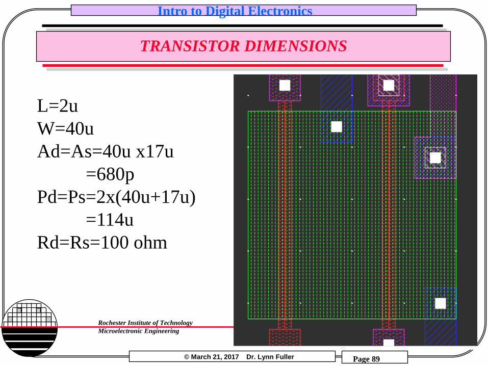
TRANSISTOR DIMENSIONS
L=2u
W=40u
Ad=As=40u x17u
=680p
Pd=Ps=2x(40u+17u)
=114u
Rd=Rs=100 ohm