introduction to comparators, their parameters and basic ... · an4071 comparator parameters doc id...
TRANSCRIPT

October 2012 Doc ID 022939 Rev 1 1/27
AN4071Application note
Introduction to comparators, their parameters and basicapplications
By Radim Smat
IntroductionAfter operational amplifiers (op amps), comparators are the most generally used analog, simple integrated circuits.
Operational amplifiers are well described in many publications and a lot of information can be found regarding the design and proper use of these devices. On the other hand, information concerning comparators is much harder to find as they are often considered as simple devices. This note explains the main parameters of comparators and their limitations from an application point of view.
Figure 1. TS332 and TS334 micropower low-voltage rail-to-rail comparators
www.st.com
Contents AN4071
2/27 Doc ID 022939 Rev 1
Contents
1 Comparator substitution by an op amp . . . . . . . . . . . . . . . . . . . . . . . . . 4
2 Comparator parameters . . . . . . . . . . . . . . . . . . . . . . . . . . . . . . . . . . . . . . 5
Comparator classification by major parameters . . . . . . . . . . . . . . . . . . . . . . . . . . . 5
3 Datasheet parameters . . . . . . . . . . . . . . . . . . . . . . . . . . . . . . . . . . . . . . . . 8
3.1 Input common mode voltage range - VICM . . . . . . . . . . . . . . . . . . . . . . . . . 8
3.2 Input offset voltage - VIO (VTRIP) . . . . . . . . . . . . . . . . . . . . . . . . . . . . . . . . 8
3.3 CMRR and SVR . . . . . . . . . . . . . . . . . . . . . . . . . . . . . . . . . . . . . . . . . . . . 10
3.4 Voltage gain . . . . . . . . . . . . . . . . . . . . . . . . . . . . . . . . . . . . . . . . . . . . . . . 11
3.5 Propagation delay . . . . . . . . . . . . . . . . . . . . . . . . . . . . . . . . . . . . . . . . . . 11
4 Hysteresis . . . . . . . . . . . . . . . . . . . . . . . . . . . . . . . . . . . . . . . . . . . . . . . . 16
4.1 Built-in hysteresis . . . . . . . . . . . . . . . . . . . . . . . . . . . . . . . . . . . . . . . . . . . 16
4.2 External hysteresis . . . . . . . . . . . . . . . . . . . . . . . . . . . . . . . . . . . . . . . . . . 17
4.3 Dynamical hysteresis, example of oscillation issue and the solution . . . . 19
5 Relaxation oscillator . . . . . . . . . . . . . . . . . . . . . . . . . . . . . . . . . . . . . . . . 22
6 Window comparator . . . . . . . . . . . . . . . . . . . . . . . . . . . . . . . . . . . . . . . . 24
7 Revision history . . . . . . . . . . . . . . . . . . . . . . . . . . . . . . . . . . . . . . . . . . . 26
AN4071 List of figures
Doc ID 022939 Rev 1 3/27
List of figures
Figure 1. TS332 and TS334 micropower low-voltage rail-to-rail comparators . . . . . . . . . . . . . . . . . . . 1Figure 2. Comparator pinout example . . . . . . . . . . . . . . . . . . . . . . . . . . . . . . . . . . . . . . . . . . . . . . . . . 5Figure 3. Signal comparison by TS3011 with built-in hysteresis
(blue IN+, green IN-, red OUT) . . . . . . . . . . . . . . . . . . . . . . . . . . . . . . . . . . . . . . . . . . . . . . . 6Figure 4. Open drain . . . . . . . . . . . . . . . . . . . . . . . . . . . . . . . . . . . . . . . . . . . . . . . . . . . . . . . . . . . . . . 7Figure 5. Push-pull . . . . . . . . . . . . . . . . . . . . . . . . . . . . . . . . . . . . . . . . . . . . . . . . . . . . . . . . . . . . . . . . 7Figure 6. Wired-OR configuration . . . . . . . . . . . . . . . . . . . . . . . . . . . . . . . . . . . . . . . . . . . . . . . . . . . . 7Figure 7. Voltage marking . . . . . . . . . . . . . . . . . . . . . . . . . . . . . . . . . . . . . . . . . . . . . . . . . . . . . . . . . . 8Figure 8. Input-trip point VTRIP . . . . . . . . . . . . . . . . . . . . . . . . . . . . . . . . . . . . . . . . . . . . . . . . . . . . . . . 8Figure 9. Input offset voltage VIO . . . . . . . . . . . . . . . . . . . . . . . . . . . . . . . . . . . . . . . . . . . . . . . . . . . . . 8Figure 10. VIO (VTRIP) measurement circuit . . . . . . . . . . . . . . . . . . . . . . . . . . . . . . . . . . . . . . . . . . . . . . 9Figure 11. TS3011 trip point voltage vs. common mode voltage . . . . . . . . . . . . . . . . . . . . . . . . . . . . . 10Figure 12. TPLH diagram . . . . . . . . . . . . . . . . . . . . . . . . . . . . . . . . . . . . . . . . . . . . . . . . . . . . . . . . . . . 12Figure 13. TPHL diagram . . . . . . . . . . . . . . . . . . . . . . . . . . . . . . . . . . . . . . . . . . . . . . . . . . . . . . . . . . . 12Figure 14. TS3011 TPD vs. overdrive voltage . . . . . . . . . . . . . . . . . . . . . . . . . . . . . . . . . . . . . . . . . . . 13Figure 15. TS3011 TPD vs. input common mode voltage . . . . . . . . . . . . . . . . . . . . . . . . . . . . . . . . . . 13Figure 16. Circuit for TPD measurement . . . . . . . . . . . . . . . . . . . . . . . . . . . . . . . . . . . . . . . . . . . . . . . 14Figure 17. Trip point voltage definition . . . . . . . . . . . . . . . . . . . . . . . . . . . . . . . . . . . . . . . . . . . . . . . . . 16Figure 18. Input hysteresis. . . . . . . . . . . . . . . . . . . . . . . . . . . . . . . . . . . . . . . . . . . . . . . . . . . . . . . . . . 16Figure 19. Non-inverting comparator with hysteresis. . . . . . . . . . . . . . . . . . . . . . . . . . . . . . . . . . . . . . 17Figure 20. Inverting comparator with hysteresis . . . . . . . . . . . . . . . . . . . . . . . . . . . . . . . . . . . . . . . . . 17Figure 21. Hysteresis circuit example . . . . . . . . . . . . . . . . . . . . . . . . . . . . . . . . . . . . . . . . . . . . . . . . . 19Figure 22. Dynamical hysteresis circuit . . . . . . . . . . . . . . . . . . . . . . . . . . . . . . . . . . . . . . . . . . . . . . . . 19Figure 23. Device oscillation without CFB capacitor (green OUT, blue IN+), time scale 500 ns/div. . . 20Figure 24. Case with CFB (green OUT, blue IN+), time scale 500 ns/div. . . . . . . . . . . . . . . . . . . . . . . 20Figure 25. Zoom of the signal (green OUT, blue IN+), time scale 20 ns/div. . . . . . . . . . . . . . . . . . . . . 21Figure 26. Relaxation oscillator . . . . . . . . . . . . . . . . . . . . . . . . . . . . . . . . . . . . . . . . . . . . . . . . . . . . . . 22Figure 27. Window comparator . . . . . . . . . . . . . . . . . . . . . . . . . . . . . . . . . . . . . . . . . . . . . . . . . . . . . . 24Figure 28. Temperature control circuit . . . . . . . . . . . . . . . . . . . . . . . . . . . . . . . . . . . . . . . . . . . . . . . . . 24
Comparator substitution by an op amp AN4071
4/27 Doc ID 022939 Rev 1
1 Comparator substitution by an op amp
To use operational amplifiers in open loop as comparators is quite common. This especially applies when an op amp is already used in the application, giving the user the opportunity to use a dual channel (or quad channel) op amp which can save space in the application. This is possible even if a better alternative is to use comparators that are optimized for this purpose.
The op amp is a device which is designed to be used with negative feedback. A major concern is to ensure the stability of such a configuration. Other parameters like slew rate and maximum bandwidth are trade-offs with current consumption and the architecture of an op amp.
Comparators, on the other hand, are designed to operate in open loop configuration without any negative feedback. In most cases, they are not internally compensated. The speed (propagation delay) and slew rate (rise and fall time) are maximized. The overall gain is also usually higher. The use of an op amp as a comparator leads to an unoptimized situation, where current consumption versus speed ratio is low. The opposite is even worse. Normally, a comparator cannot be used instead of an op amp. Most probably, the comparator shows instability under negative feedback. Generally speaking, comparators and operational amplifiers cannot substitute each other except for low performance designs.
AN4071 Comparator parameters
Doc ID 022939 Rev 1 5/27
2 Comparator parameters
Comparator classification by major parameters● Propagation delay
● Current consumption
● Output stage type (open collector/drain or push-pull)
● Input offset voltage, hysteresis
● Output current capability
● Rise and fall time
● Input common mode voltage range.
Besides major parameters, comparators are classified by other parameters such as input bias current, common mode and power supply rejection ratio, sample/hold function, and startup time.
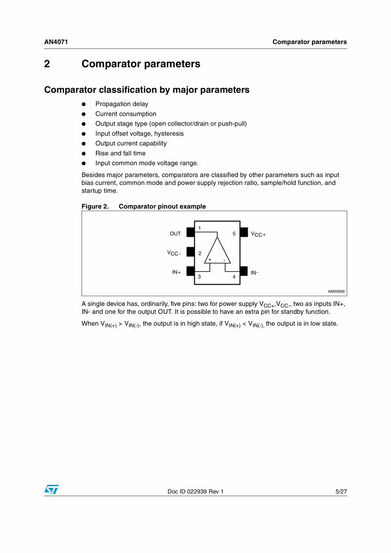
Figure 2. Comparator pinout example
A single device has, ordinarily, five pins: two for power supply VCC+,VCC-, two as inputs IN+, IN- and one for the output OUT. It is possible to have an extra pin for standby function.
When VIN(+) > VIN(-), the output is in high state, if VIN(+) < VIN(-), the output is in low state.
Comparator parameters AN4071
6/27 Doc ID 022939 Rev 1
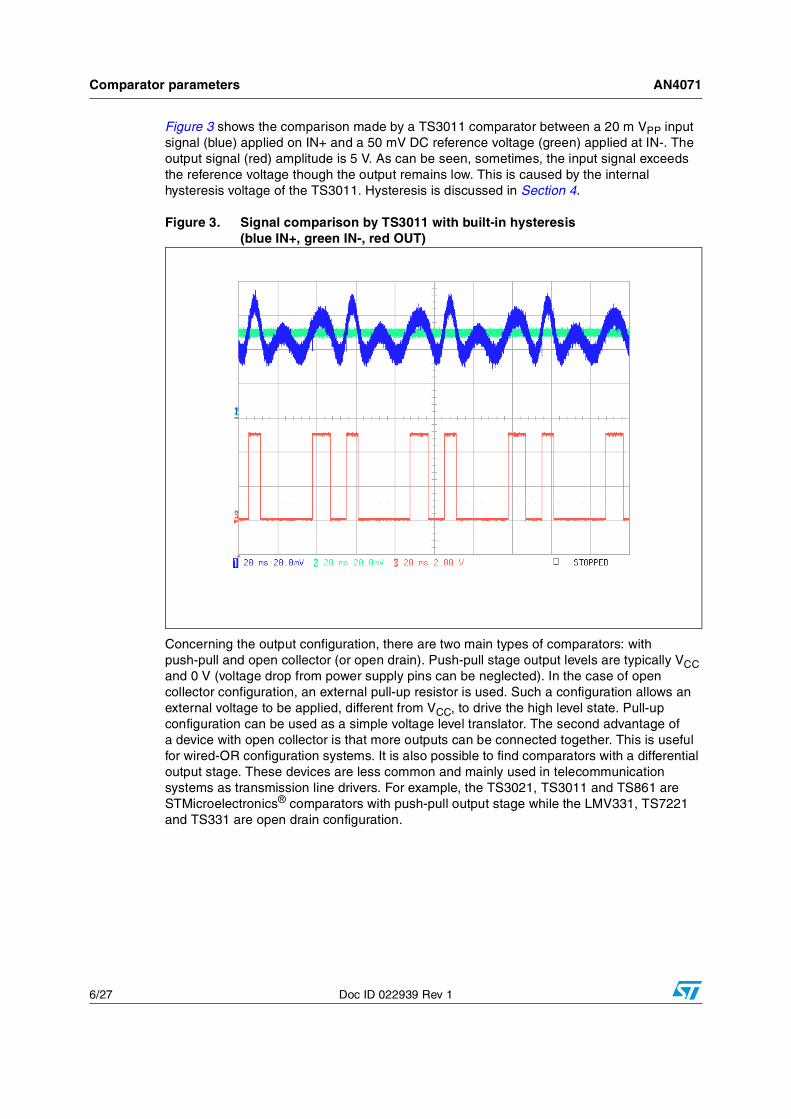
Figure 3 shows the comparison made by a TS3011 comparator between a 20 m VPP input signal (blue) applied on IN+ and a 50 mV DC reference voltage (green) applied at IN-. The output signal (red) amplitude is 5 V. As can be seen, sometimes, the input signal exceeds the reference voltage though the output remains low. This is caused by the internal hysteresis voltage of the TS3011. Hysteresis is discussed in Section 4.
Figure 3. Signal comparison by TS3011 with built-in hysteresis (blue IN+, green IN-, red OUT)
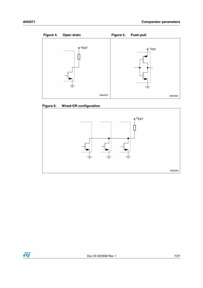
Concerning the output configuration, there are two main types of comparators: with push-pull and open collector (or open drain). Push-pull stage output levels are typically VCC and 0 V (voltage drop from power supply pins can be neglected). In the case of open collector configuration, an external pull-up resistor is used. Such a configuration allows an external voltage to be applied, different from VCC, to drive the high level state. Pull-up configuration can be used as a simple voltage level translator. The second advantage of a device with open collector is that more outputs can be connected together. This is useful for wired-OR configuration systems. It is also possible to find comparators with a differential output stage. These devices are less common and mainly used in telecommunication systems as transmission line drivers. For example, the TS3021, TS3011 and TS861 are STMicroelectronics® comparators with push-pull output stage while the LMV331, TS7221 and TS331 are open drain configuration.
AN4071 Comparator parameters
Doc ID 022939 Rev 1 7/27
Figure 6. Wired-OR configuration
Figure 4. Open drain Figure 5. Push-pull

Datasheet parameters AN4071
8/27 Doc ID 022939 Rev 1
3 Datasheet parameters
3.1 Input common mode voltage range - VICM The VICM is defined as the voltage range where both inputs must remain to guarantee the functionality of the device. When the input common mode range covers both power supply rails 0 V and VCC, it is a rail-to-rail input stage.
Regarding the use of a rail-to-rail (R2R) comparator, from a technical point of view, if the R2R input capability is not needed, it is always better to choose a comparator without R2R input stage. The power consumption is, in that case, obviously smaller and the device cost is lower.
3.2 Input offset voltage - VIO (VTRIP)The input offset voltage (VIO) can be defined as the differential input voltage to apply in order to be at the toggling level. Input offset voltage limits the resolution of comparators. Therefore, for very small signals (in the same order as the VIO), the comparator toggles at an undesired value or does not toggle at all.
Figure 7. Voltage marking
Figure 8. Input-trip point VTRIP Figure 9. Input offset voltage VIO
AN4071 Datasheet parameters
Doc ID 022939 Rev 1 9/27
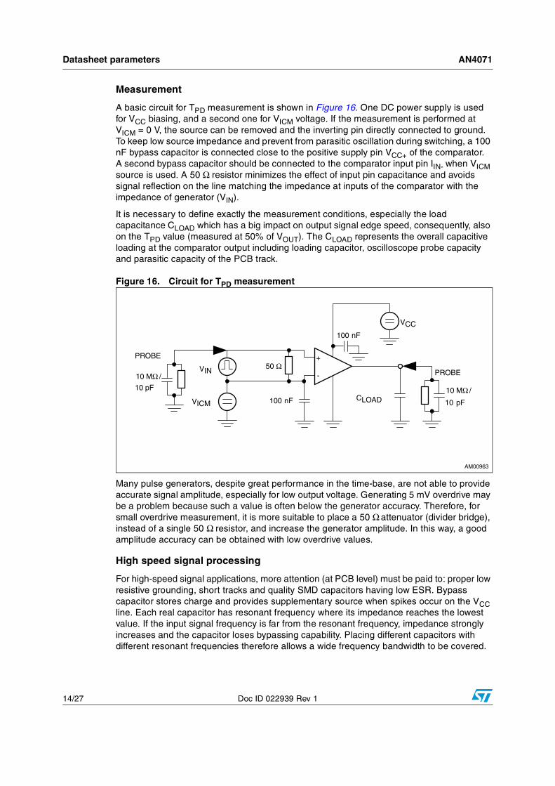
In other words, input offset voltage can be represented by a voltage source applied in series with one input of an ideal comparator. Consequently, the output doesn't toggle when VIN+ = VIN-, as in the case of an ideal comparator, but the threshold level is shifted by the input offset value VIO. Input offset voltage rises in the input stage as a consequence of transistor imbalance. For comparators with built-in hysteresis, VIO is defined as the average value of VTRIP+ and VTRIP-, and the hysteresis of VHYST = VTRIP+ - VTRIP- where VTRIP+ (respectively VTRIP-) is the input differential voltage for which the output switches from low to high state (respectively high to low state).
Measurement
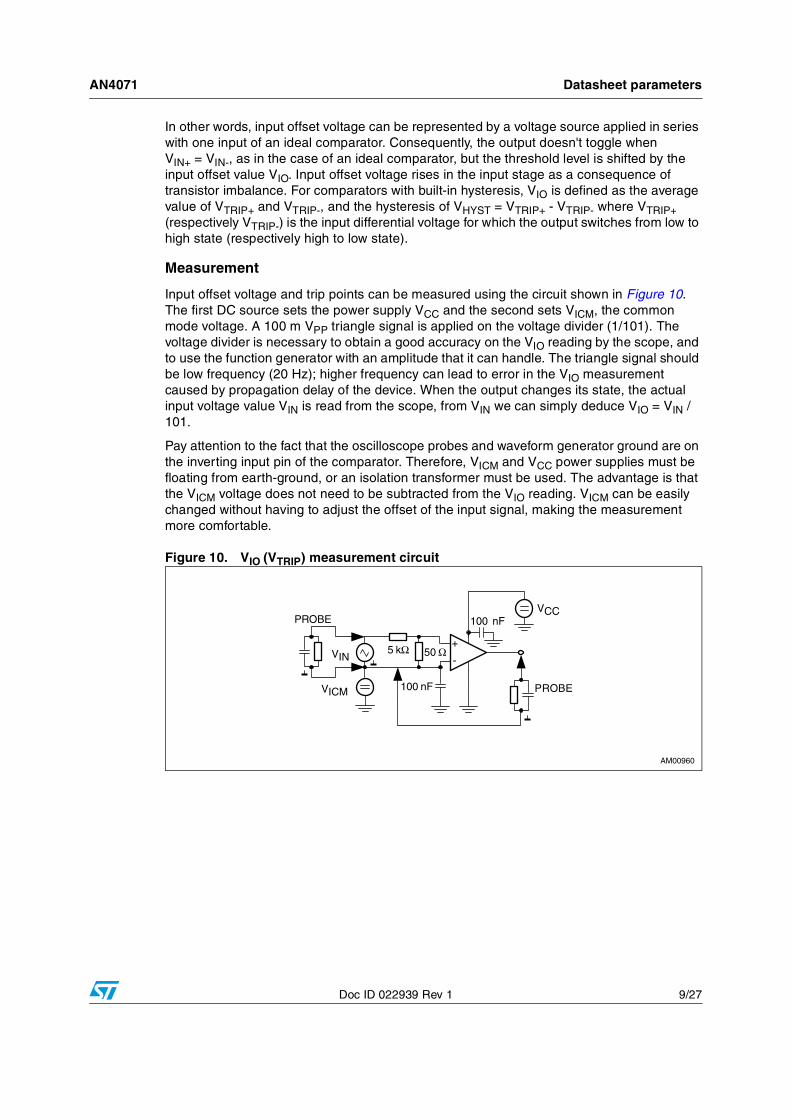
Input offset voltage and trip points can be measured using the circuit shown in Figure 10. The first DC source sets the power supply VCC and the second sets VICM, the common mode voltage. A 100 m VPP triangle signal is applied on the voltage divider (1/101). The voltage divider is necessary to obtain a good accuracy on the VIO reading by the scope, and to use the function generator with an amplitude that it can handle. The triangle signal should be low frequency (20 Hz); higher frequency can lead to error in the VIO measurement caused by propagation delay of the device. When the output changes its state, the actual input voltage value VIN is read from the scope, from VIN we can simply deduce VIO = VIN / 101.
Pay attention to the fact that the oscilloscope probes and waveform generator ground are on the inverting input pin of the comparator. Therefore, VICM and VCC power supplies must be floating from earth-ground, or an isolation transformer must be used. The advantage is that the VICM voltage does not need to be subtracted from the VIO reading. VICM can be easily changed without having to adjust the offset of the input signal, making the measurement more comfortable.
Figure 10. VIO (VTRIP) measurement circuit
Datasheet parameters AN4071
10/27 Doc ID 022939 Rev 1
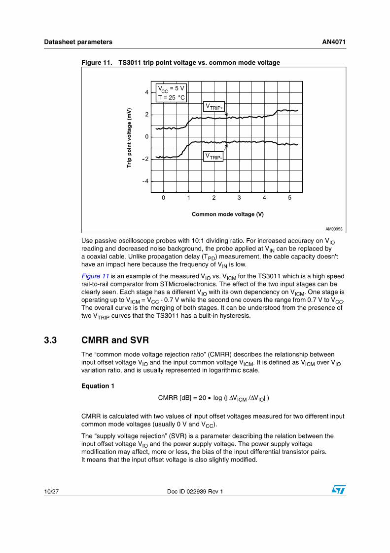
Figure 11. TS3011 trip point voltage vs. common mode voltage
Use passive oscilloscope probes with 10:1 dividing ratio. For increased accuracy on VIO reading and decreased noise background, the probe applied at VIN can be replaced by a coaxial cable. Unlike propagation delay (TPD) measurement, the cable capacity doesn't have an impact here because the frequency of VIN is low.
Figure 11 is an example of the measured VIO vs. VICM for the TS3011 which is a high speed rail-to-rail comparator from STMicroelectronics. The effect of the two input stages can be clearly seen. Each stage has a different VIO with its own dependency on VICM. One stage is operating up to VICM = VCC - 0.7 V while the second one covers the range from 0.7 V to VCC. The overall curve is the merging of both stages. It can be understood from the presence of two VTRIP curves that the TS3011 has a built-in hysteresis.
3.3 CMRR and SVRThe “common mode voltage rejection ratio” (CMRR) describes the relationship between input offset voltage VIO and the input common voltage VICM. It is defined as VICM over VIO variation ratio, and is usually represented in logarithmic scale.
Equation 1
CMRR [dB] = 20 • log (| ΔVICM /ΔVIO| )
CMRR is calculated with two values of input offset voltages measured for two different input common mode voltages (usually 0 V and VCC).
The “supply voltage rejection” (SVR) is a parameter describing the relation between the input offset voltage VIO and the power supply voltage. The power supply voltage modification may affect, more or less, the bias of the input differential transistor pairs. It means that the input offset voltage is also slightly modified.
AN4071 Datasheet parameters
Doc ID 022939 Rev 1 11/27
Equation 2
SVR [dB] = 20 • log (| ΔVCC /ΔVIO| )
Note that, the higher CMMR and SVR are the better.
Measurement
The circuit is the same as the one used for VIO (Figure 10).
1. CMRRVIO at low (L) VICM rail and VIO at high (H) VICM rail are measuredthen CMRR = 20 • log [(VICM(H) - VICM(L)) / (|VIO(H)-VIO(L)|)]
2. SVRVIO at low VCC and VIO at high VCC are measured then SVR = 20 • log [(VCC(H)- VCC(L)) / (| VIO(H)-VIO(L)|)]
3.4 Voltage gainVoltage gain AVD indicates the overall device gain. Higher gain means better small input signal resolving capability which can be an advantage in certain applications. Common comparators have an AVD in the range of 200 V/mV (106 dB). 1 mV input signal amplified by 106 dB leads to theoretical amplitude of 200 V. In reality, the output signal swing is limited by VCC. Note that the AVD doesn’t affect external hysteresis as the output is always in high or low state and never between (unlike an operational amplifier, a comparator is not used in its linear region).
3.5 Propagation delayPropagation delay TPD is one of the key parameters for many applications because it limits the maximal input frequency which can be processed. Voltage comparison of analog signals requires a minimum amount of time.
TPD is defined as the time difference between the moment the input signal crossing the reference voltage and the moment the output state changes (usually when the output signal crosses 50% of VCC, if nothing is specified).
A graphical interpretation is shown in Figure 12 and 13. For TPLH an input square signal from -100 mV to +VOV, called overdrive voltage and referenced to VICM + VTRIP+, is applied on the non-inverting input. The inverting input is connected at VICM voltage. Initial signal condition 100 mV below VICM +VTRIP+ ensures a sufficient saturation for the input stage. For the falling edge propagation delay measurement (TPHL), the input signal goes from +100 mV to -VOV referenced to VICM + VTRIP-.

Datasheet parameters AN4071
12/27 Doc ID 022939 Rev 1
Figure 12. TPLH diagram
Figure 13. TPHL diagram
AN4071 Datasheet parameters
Doc ID 022939 Rev 1 13/27
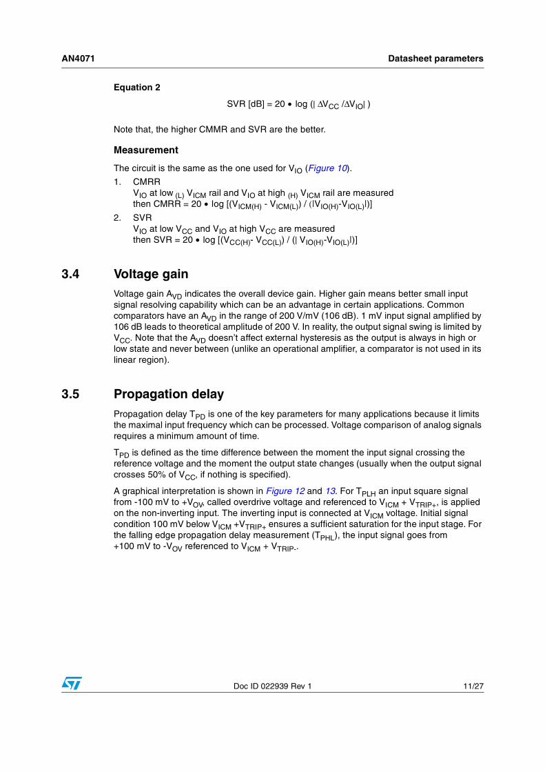
The input signal is referenced to VICM + VTRIP and not only to VICM because, in the case of small signal overdrive, an error in TPD measurement can occur due to non-zero VIO (VTRIP+ and/or VTRIP- <> 0). In reality, we can neglect VIO without significant impact on TPD for VOV values of 20 mV and higher, considering that the offset value reaches around 1 mV and considering the exponential dependency of TPD on overdrive voltage, as shown in Figure 14.
Figure 14. TS3011 TPD vs. overdrive voltage
Figure 15. TS3011 TPD vs. input common mode voltage
Datasheet parameters AN4071
14/27 Doc ID 022939 Rev 1
Measurement
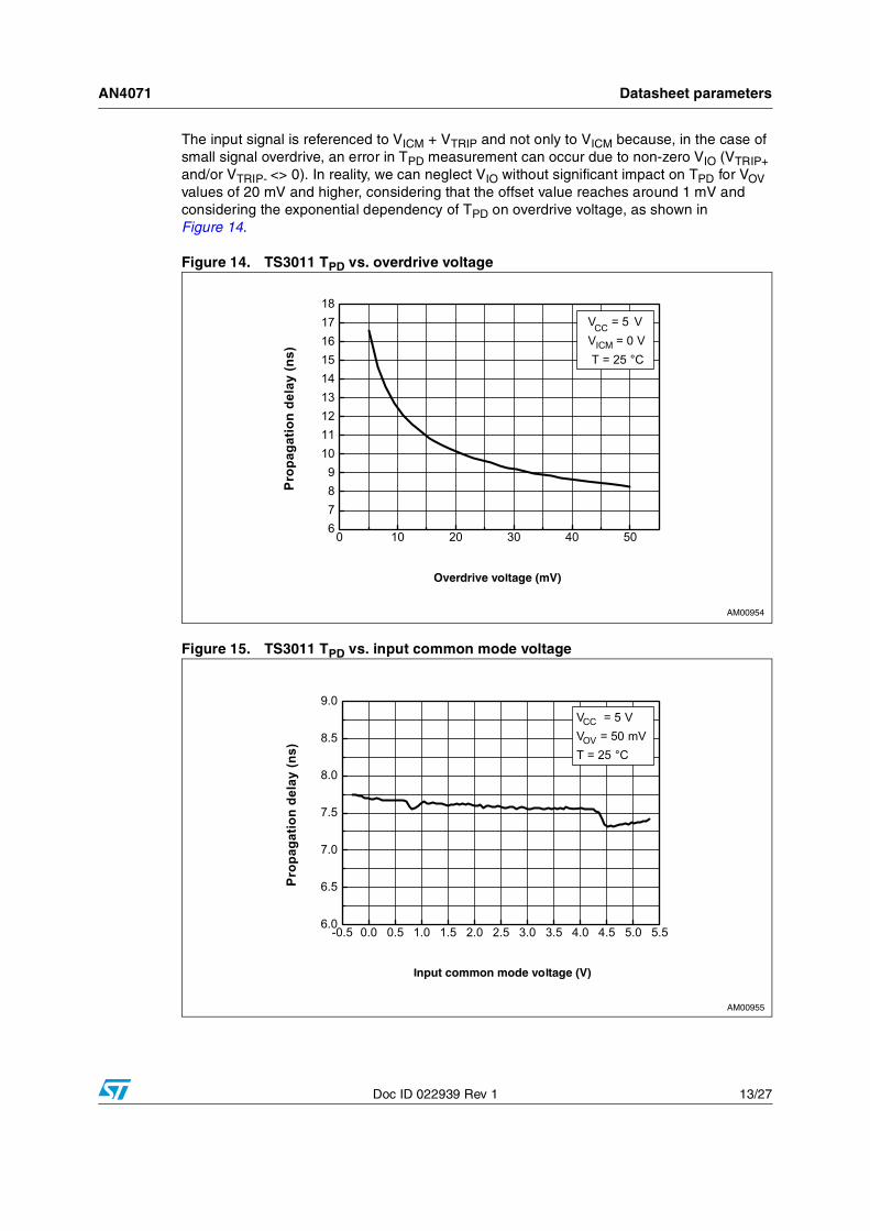
A basic circuit for TPD measurement is shown in Figure 16. One DC power supply is used for VCC biasing, and a second one for VICM voltage. If the measurement is performed at VICM = 0 V, the source can be removed and the inverting pin directly connected to ground. To keep low source impedance and prevent from parasitic oscillation during switching, a 100 nF bypass capacitor is connected close to the positive supply pin VCC+ of the comparator. A second bypass capacitor should be connected to the comparator input pin IIN- when VICM source is used. A 50 Ω resistor minimizes the effect of input pin capacitance and avoids signal reflection on the line matching the impedance at inputs of the comparator with the impedance of generator (VIN).
It is necessary to define exactly the measurement conditions, especially the load capacitance CLOAD which has a big impact on output signal edge speed, consequently, also on the TPD value (measured at 50% of VOUT). The CLOAD represents the overall capacitive loading at the comparator output including loading capacitor, oscilloscope probe capacity and parasitic capacity of the PCB track.
Figure 16. Circuit for TPD measurement
Many pulse generators, despite great performance in the time-base, are not able to provide accurate signal amplitude, especially for low output voltage. Generating 5 mV overdrive may be a problem because such a value is often below the generator accuracy. Therefore, for small overdrive measurement, it is more suitable to place a 50 Ω attenuator (divider bridge), instead of a single 50 Ω resistor, and increase the generator amplitude. In this way, a good amplitude accuracy can be obtained with low overdrive values.
High speed signal processing
For high-speed signal applications, more attention (at PCB level) must be paid to: proper low resistive grounding, short tracks and quality SMD capacitors having low ESR. Bypass capacitor stores charge and provides supplementary source when spikes occur on the VCC line. Each real capacitor has resonant frequency where its impedance reaches the lowest value. If the input signal frequency is far from the resonant frequency, impedance strongly increases and the capacitor loses bypassing capability. Placing different capacitors with different resonant frequencies therefore allows a wide frequency bandwidth to be covered.

AN4071 Datasheet parameters
Doc ID 022939 Rev 1 15/27
Such a bypass combination, made from 100 nF, 10 nF and 1 nF in parallel, eliminates unwanted spikes on the VCC line much better than only one 100 nF capacitor.
Each mm of the track plays a role. Bypass capacitors must be placed as close as possible to the comparator supply pin. Place the smallest capacitor closer to the supply pin than the bigger one. Removing GND copper under signal track minimizes overall capacitive loading. Input source impedance shouldn't exceed 1 kΩ, otherwise undesirable oscillations can appear. In addition, too high input impedance in series with parasitic PCB capacity and input comparator capacity produces additional RC constant which means additional propagation delay.
Concerning time measurements on high-speed comparators, remember that for a high speed signal the oscilloscope and probe can cause significant error in measurement accuracy when their bandwidth is too low. The measured TRISE (TFALL) value is affected by the rise time of the scope and the probe by:
Equation 3
TRISE = (TRISE SIGNAL2+ TRISE SCOPE
2+ TRISE PROBE2)1/2
Hysteresis AN4071
16/27 Doc ID 022939 Rev 1
4 Hysteresis
For slow time changing input signal, an output oscillation can appear while the input signal remains close to the reference voltage. Also low amplitude signal on high impedance can cause oscillations due to noise background. Such unwelcome behavior can be solved by hysteresis. The principle of hysteresis consists of two different input threshold voltages depending on actual output state.
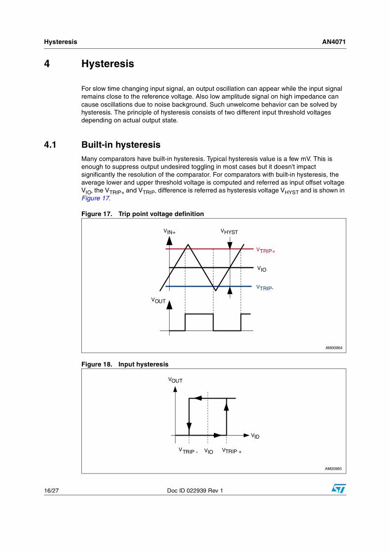
4.1 Built-in hysteresisMany comparators have built-in hysteresis. Typical hysteresis value is a few mV. This is enough to suppress output undesired toggling in most cases but it doesn't impact significantly the resolution of the comparator. For comparators with built-in hysteresis, the average lower and upper threshold voltage is computed and referred as input offset voltage VIO, the VTRIP+ and VTRIP- difference is referred as hysteresis voltage VHYST and is shown in Figure 17.
Figure 17. Trip point voltage definition
Figure 18. Input hysteresis
AN4071 Hysteresis
Doc ID 022939 Rev 1 17/27
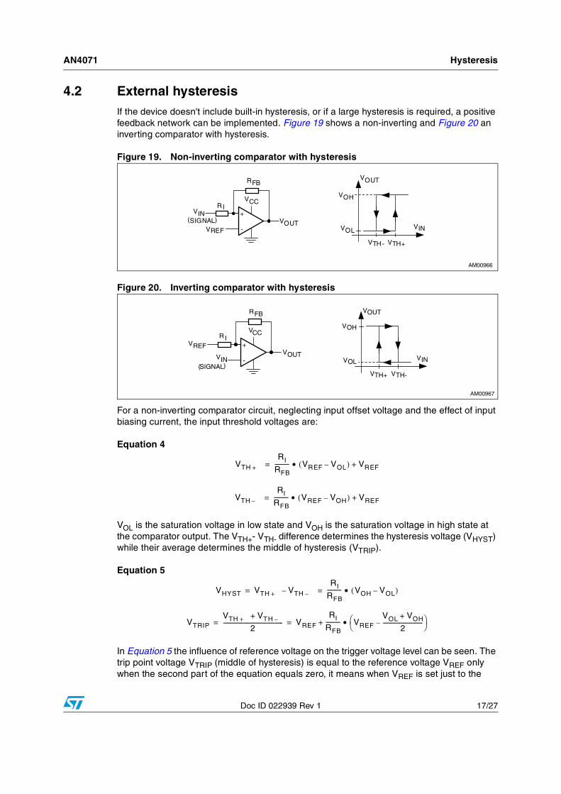
4.2 External hysteresisIf the device doesn't include built-in hysteresis, or if a large hysteresis is required, a positive feedback network can be implemented. Figure 19 shows a non-inverting and Figure 20 an inverting comparator with hysteresis.
Figure 19. Non-inverting comparator with hysteresis
Figure 20. Inverting comparator with hysteresis
For a non-inverting comparator circuit, neglecting input offset voltage and the effect of input biasing current, the input threshold voltages are:
Equation 4
VOL is the saturation voltage in low state and VOH is the saturation voltage in high state at the comparator output. The VTH+- VTH- difference determines the hysteresis voltage (VHYST) while their average determines the middle of hysteresis (VTRIP).
Equation 5
In Equation 5 the influence of reference voltage on the trigger voltage level can be seen. The trip point voltage VTRIP (middle of hysteresis) is equal to the reference voltage VREF only when the second part of the equation equals zero, it means when VREF is set just to the
VTH +
RI
RFB---------- VREF VOL–( ) VREF+•=
VTH –
RI
RFB---------- VREF VOH–( ) VREF+•=
VHYST VTH + VTH ––RI
RFB---------- VOH VOL–( )•= =
VTRIPVTH + VTH –+
2------------------------------------------ VREF
RI
RFB---------- VREF
VOL VOH+
2----------------------------–⎝ ⎠
⎛ ⎞•+= =
Hysteresis AN4071
18/27 Doc ID 022939 Rev 1
centre of output voltage swing. Otherwise VREF and VTRIP are different and the hysteresis is not centred on VREF.
For calculating RI, RFB and VREF, two formulas, obtained from Equation 4 and 5, can be used:
Equation 6
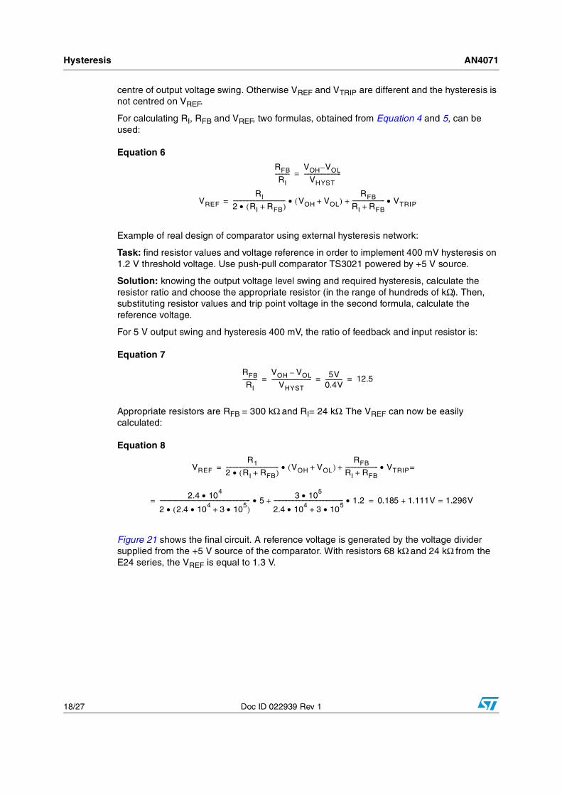
Example of real design of comparator using external hysteresis network:
Task: find resistor values and voltage reference in order to implement 400 mV hysteresis on 1.2 V threshold voltage. Use push-pull comparator TS3021 powered by +5 V source.
Solution: knowing the output voltage level swing and required hysteresis, calculate the resistor ratio and choose the appropriate resistor (in the range of hundreds of kΩ). Then, substituting resistor values and trip point voltage in the second formula, calculate the reference voltage.
For 5 V output swing and hysteresis 400 mV, the ratio of feedback and input resistor is:
Equation 7
Appropriate resistors are RFB = 300 kΩ and RI= 24 kΩ. The VREF can now be easily calculated:
Equation 8
Figure 21 shows the final circuit. A reference voltage is generated by the voltage divider supplied from the +5 V source of the comparator. With resistors 68 kΩ and 24 kΩ from the E24 series, the VREF is equal to 1.3 V.
RFB
RI----------
VOH VOL–
VHYST--------------------------=
VREF
RI
2 RI RFB+( )•------------------------------------- VOH VOL+( )
RFB
RI RFB+----------------------- VTRIP•+•=
RFB
RI----------
VOH VOL–
VHYST---------------------------- 5V
0.4V------------ 12.5= = =
VREF
R1
2 RI RFB+( )•------------------------------------- VOH VOL+( )
RFB
RI RFB+----------------------- VTRIP•+• ==
2.4 104•
2 2.4 104 3 105•+•( )•---------------------------------------------------------------- 5
3 105•
2.4 104 3 105•+•------------------------------------------------- 1.2•+• 0.185 1.111V 1.296V=+= =
AN4071 Hysteresis
Doc ID 022939 Rev 1 19/27
Figure 21. Hysteresis circuit example
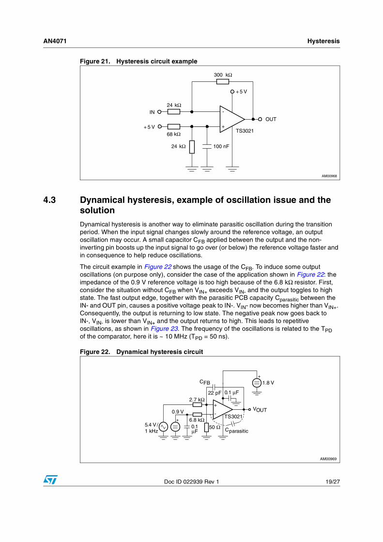
4.3 Dynamical hysteresis, example of oscillation issue and the solutionDynamical hysteresis is another way to eliminate parasitic oscillation during the transition period. When the input signal changes slowly around the reference voltage, an output oscillation may occur. A small capacitor CFB applied between the output and the non-inverting pin boosts up the input signal to go over (or below) the reference voltage faster and in consequence to help reduce oscillations.
The circuit example in Figure 22 shows the usage of the CFB. To induce some output oscillations (on purpose only), consider the case of the application shown in Figure 22: the impedance of the 0.9 V reference voltage is too high because of the 6.8 kΩ resistor. First, consider the situation without CFB when VIN+ exceeds VIN- and the output toggles to high state. The fast output edge, together with the parasitic PCB capacity Cparasitic between the IN- and OUT pin, causes a positive voltage peak to IN-. VIN- now becomes higher than VIN+. Consequently, the output is returning to low state. The negative peak now goes back to IN-, VIN- is lower than VIN+ and the output returns to high. This leads to repetitive oscillations, as shown in Figure 23. The frequency of the oscillations is related to the TPD of the comparator, here it is ~ 10 MHz (TPD = 50 ns).
Figure 22. Dynamical hysteresis circuit
Hysteresis AN4071
20/27 Doc ID 022939 Rev 1
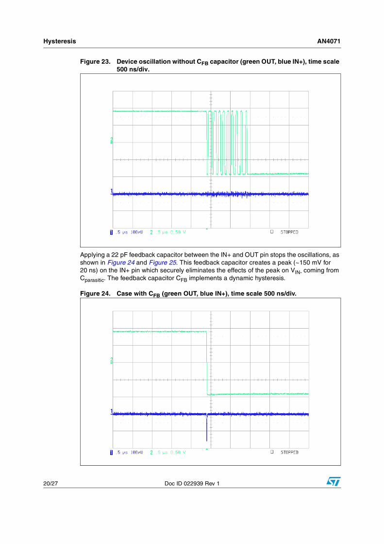
Figure 23. Device oscillation without CFB capacitor (green OUT, blue IN+), time scale 500 ns/div.
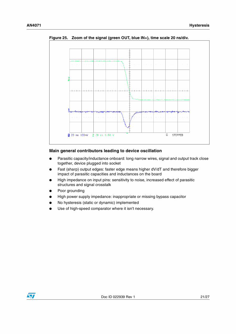
Applying a 22 pF feedback capacitor between the IN+ and OUT pin stops the oscillations, as shown in Figure 24 and Figure 25. This feedback capacitor creates a peak (~150 mV for 20 ns) on the IN+ pin which securely eliminates the effects of the peak on VIN- coming from Cparasitic. The feedback capacitor CFB implements a dynamic hysteresis.
Figure 24. Case with CFB (green OUT, blue IN+), time scale 500 ns/div.
AN4071 Hysteresis
Doc ID 022939 Rev 1 21/27
Figure 25. Zoom of the signal (green OUT, blue IN+), time scale 20 ns/div.
Main general contributors leading to device oscillation
● Parasitic capacity/inductance onboard: long narrow wires, signal and output track close together, device plugged into socket
● Fast (sharp) output edges: faster edge means higher dV/dT and therefore bigger impact of parasitic capacities and inductances on the board
● High impedance on input pins: sensitivity to noise, increased effect of parasitic structures and signal crosstalk
● Poor grounding
● High power supply impedance: inappropriate or missing bypass capacitor
● No hysteresis (static or dynamic) implemented
● Use of high-speed comparator where it isn't necessary.
Relaxation oscillator AN4071
22/27 Doc ID 022939 Rev 1
5 Relaxation oscillator
A relaxation oscillator belongs to the regenerative circuits group. One subgroup is multivibrators which are furthermore classified as monostable, bistable and astable. The relaxation oscillator is an astable multivibrator.
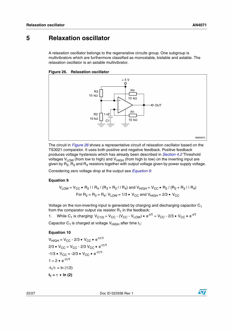
Figure 26. Relaxation oscillator
The circuit in Figure 26 shows a representative circuit of relaxation oscillator based on the TS3021 comparator. It uses both positive and negative feedback. Positive feedback produces voltage hysteresis which has already been described in Section 4.2 Threshold voltages VLOW (from low to high) and VHIGH (from high to low) on the inverting input are given by R2, R3 and R4 resistors together with output voltage given by power supply voltage.
Considering zero voltage drop at the output see Equation 9:
Equation 9
VLOW = VCC • R2 | | R4 / (R3 + R2 | | R4) and VHIGH = VCC • R2 / (R2 + R3 | | R4)
For R2 = R3 = R4: VLOW = 1/3 • VCC and VHIGH = 2/3 • VCC
Voltage on the non-inverting input is generated by charging and discharging capacitor C1 from the comparator output via resistor R1 in the feedback:
1. While C1 is charging: VC1(t) = VCC - (VCC - VLOW) • e-t/τ = VCC - 2/3 • VCC • e-t/τ
Capacitor C1 is charged at voltage VHIGH after time t1:
Equation 10
VHIGH = VCC - 2/3 • VCC • e-t1/τ
2/3 • VCC = VCC - 2/3 VCC • e-t1/τ
-1/3 • VCC = -2/3 • VCC • e-t1/τ
1 = 2 • e-t1/τ
-t1/τ = ln (1/2)
t1 = τ • ln (2)
AN4071 Relaxation oscillator
Doc ID 022939 Rev 1 23/27
2. While C1 is discharging: VC1(t) = VHIGH • e-t/τ = 2/3 • VCC • e -t/τ
Capacitor C1 is discharged at voltage VLOW after time t2:
Equation 11
VLOW = 2/3 • VCC • e-t2/τ
1/3 • VCC = 2/3 • VCC • e-t2/τ
1 = 2 • e-t2/τ
-t2/τ = ln (1/2)
t2 = τ • ln (2)
Because t1 = t2, the output square signal has 50% duty cycle. The output signal period T is the sum of the time t1 and the time t2:
T = t1 + t2= τ • ln (4), where τ = R1 • C1
In the configuration described in Figure 11, the output frequency is around 72 kHz.
Output frequency doesn't depend on the power supply voltage. As the TS3021 circuit can work with a wide power supply voltage range from 1.8 V to 5 V, the output signal amplitude has the same value as the power supply due to its rail-to-rail output stage. Frequency can be adjusted simply by changing the value of R1 or C1. In case a different duty cycle is required, R2, R3 and R4 should not be kept equal.
Window comparator AN4071
24/27 Doc ID 022939 Rev 1
6 Window comparator
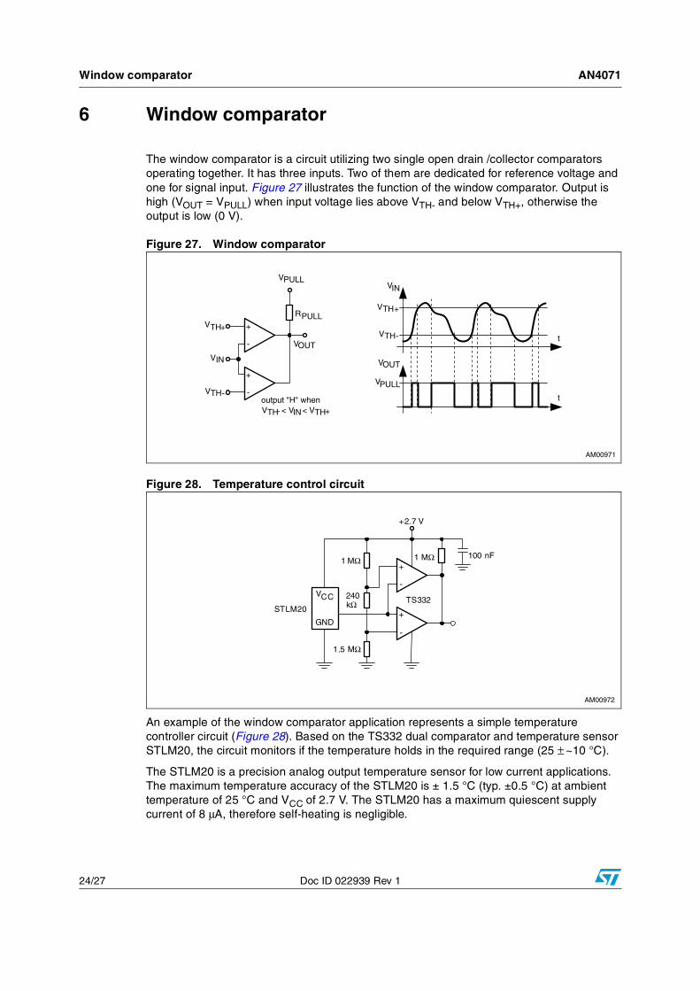
The window comparator is a circuit utilizing two single open drain /collector comparators operating together. It has three inputs. Two of them are dedicated for reference voltage and one for signal input. Figure 27 illustrates the function of the window comparator. Output is high (VOUT = VPULL) when input voltage lies above VTH- and below VTH+, otherwise the output is low (0 V).
Figure 27. Window comparator
Figure 28. Temperature control circuit
An example of the window comparator application represents a simple temperature controller circuit (Figure 28). Based on the TS332 dual comparator and temperature sensor STLM20, the circuit monitors if the temperature holds in the required range (25 ± ~10 °C).
The STLM20 is a precision analog output temperature sensor for low current applications. The maximum temperature accuracy of the STLM20 is ± 1.5 °C (typ. ±0.5 °C) at ambient temperature of 25 °C and VCC of 2.7 V. The STLM20 has a maximum quiescent supply current of 8 μA, therefore self-heating is negligible.
AN4071 Window comparator
Doc ID 022939 Rev 1 25/27
The TS332 is a dual micropower and low-voltage comparator. It can operate with a supply voltage ranging from 1.6 to 5.5 V with only 20 μA current consumption per operator. In addition, rail-to-rail inputs and a temperature range of -40 °C to +125 °C makes it ideal for a wide range of applications.
With good accuracy about 25 °C, the STLM20 transfer function can be described by the parabolic transfer function expressed in Equation 12:
Equation 12
VOUT = (-3.88 • 10-6 • T2) + (-1.15 • 10-2 • T) + 1.8639 [V, °C]
Based on the STLM20 transfer function equation, for the considered temperature range 25 ± 10 °C, the minimum output voltage VTH- is obtained at the higher temperature (35 °C) and equals 1.457 V. The maximum output voltage VTH+ is at the lowest temperature (15 °C) and equals 1.691 V.
VTH voltages are generated by a voltage divider. 1 μA current through the divider (IDIV) is a compromise between noise sensitivity and low impact on the supply current of the application. The resistors in the divider are:
R1 (lower resistor) = VTH- / IDIV = 1.457 MΩ
R2 (middle resistor) = (VTH+ - VTH-) / IDIV = 234 kΩ
R3 (upper resistor) = (VCC - VTH+) / IDIV = 1.009 MΩ
The closest values from the E24 resistor series are: R1 = 1.5 MΩ, R2 = 240 kΩ, R3 = 1 MΩ.
A recalculation of the temperature range can be made with these resistors.
Equation 13
IDIV = VCC/(R1 + R2 + R3) = 2.7 V/(1.5 MΩ + 240 kΩ + 1 MΩ) = 0.985 μA
VTH- = IDIV • R1 = 1.478 V
VTH+ = IDIV • (R1+ R2) = 1.714 V
The temperature can be expressed from the voltage of the STLM20:
Equation 14
After substitution we get: TLOW = 13 °C and THIGH = 33.2 °C.
For better range setting precision, fixed resistors in the voltage divider bridge can be replaced by variable resistors. Note that, temperature setting depends on the supply voltage. Thanks to the micro power TS332 comparator, the power current consumption of the application is typically only 50 μA at 25 °C and max. 74 μA over full temperature range.
T 1481.96– 2.1962 106 1.8639 VOUT–
3.88 106–•
---------------------------------------+• ° C V,( )+=

Revision history AN4071
26/27 Doc ID 022939 Rev 1
7 Revision history
Table 1. Document revision history
Date Revision Changes
09-Oct-2012 1 Initial release.
AN4071
Doc ID 022939 Rev 1 27/27
Please Read Carefully:
Information in this document is provided solely in connection with ST products. STMicroelectronics NV and its subsidiaries (“ST”) reserve theright to make changes, corrections, modifications or improvements, to this document, and the products and services described herein at anytime, without notice.
All ST products are sold pursuant to ST’s terms and conditions of sale.
Purchasers are solely responsible for the choice, selection and use of the ST products and services described herein, and ST assumes noliability whatsoever relating to the choice, selection or use of the ST products and services described herein.
No license, express or implied, by estoppel or otherwise, to any intellectual property rights is granted under this document. If any part of thisdocument refers to any third party products or services it shall not be deemed a license grant by ST for the use of such third party productsor services, or any intellectual property contained therein or considered as a warranty covering the use in any manner whatsoever of suchthird party products or services or any intellectual property contained therein.
UNLESS OTHERWISE SET FORTH IN ST’S TERMS AND CONDITIONS OF SALE ST DISCLAIMS ANY EXPRESS OR IMPLIEDWARRANTY WITH RESPECT TO THE USE AND/OR SALE OF ST PRODUCTS INCLUDING WITHOUT LIMITATION IMPLIEDWARRANTIES OF MERCHANTABILITY, FITNESS FOR A PARTICULAR PURPOSE (AND THEIR EQUIVALENTS UNDER THE LAWSOF ANY JURISDICTION), OR INFRINGEMENT OF ANY PATENT, COPYRIGHT OR OTHER INTELLECTUAL PROPERTY RIGHT.
UNLESS EXPRESSLY APPROVED IN WRITING BY TWO AUTHORIZED ST REPRESENTATIVES, ST PRODUCTS ARE NOTRECOMMENDED, AUTHORIZED OR WARRANTED FOR USE IN MILITARY, AIR CRAFT, SPACE, LIFE SAVING, OR LIFE SUSTAININGAPPLICATIONS, NOR IN PRODUCTS OR SYSTEMS WHERE FAILURE OR MALFUNCTION MAY RESULT IN PERSONAL INJURY,DEATH, OR SEVERE PROPERTY OR ENVIRONMENTAL DAMAGE. ST PRODUCTS WHICH ARE NOT SPECIFIED AS "AUTOMOTIVEGRADE" MAY ONLY BE USED IN AUTOMOTIVE APPLICATIONS AT USER’S OWN RISK.
Resale of ST products with provisions different from the statements and/or technical features set forth in this document shall immediately voidany warranty granted by ST for the ST product or service described herein and shall not create or extend in any manner whatsoever, anyliability of ST.
ST and the ST logo are trademarks or registered trademarks of ST in various countries.
Information in this document supersedes and replaces all information previously supplied.
The ST logo is a registered trademark of STMicroelectronics. All other names are the property of their respective owners.
© 2012 STMicroelectronics - All rights reserved
STMicroelectronics group of companies
Australia - Belgium - Brazil - Canada - China - Czech Republic - Finland - France - Germany - Hong Kong - India - Israel - Italy - Japan - Malaysia - Malta - Morocco - Philippines - Singapore - Spain - Sweden - Switzerland - United Kingdom - United States of America
www.st.com