introduction to 8051 microcontroller€¦ · features of microcontroller •8051 is an 40 pin ic....
TRANSCRIPT

UTL Technologies Ltd
Introduction To8051 Microcontroller

UTL Technologies Ltd
Objective• Introduction to Microcontrollers.
• Architecture.• Memory Organization.• Stacks.• PIN Configuration and description.
• Addressing Modes• Instruction Set.• 8051 Comparison with PIC , AVR.

UTL Technologies Ltd
Microprocessor vs. Microcontrollers
CONTROL
ADDRESS
DATA
CPUBOOTROM
Used atstartup
Instruction(program)
ROM
I/OPORTS
KeyboardScreenUART
Parallelinterface
etc
DataRAM
General purpose Microprocessor system

UTL Technologies Ltd
• Microprocessor, by-itself, completelyuseless .
• It does not have RAM,ROM and no I/Oports on the chip itself.
• Must have external peripherals to Interactwith outside world.
• Makes system bulkier and expensive.

UTL Technologies Ltd
• A Microcontroller has a CPU alongwith fixed amount of RAM, ROM ,andI/O ports and timer on a single chip.
•
Microcontroller Based System
CPU
SERIAL COMPORT
ROMRAM
I/O TIMER

UTL Technologies Ltd
Choosing a Microcontroller• There are four major 8 bit microcontrollers.
» Freescale-68111» Intel's -8051» PIC 16x» Microchip.
• Each one has its own instruction set andregister set so not compatible with eachother.

UTL Technologies Ltd
• Criteria to select a microcontroller– Meeting the computing needs of the task
» Speed, Packaging, Power consumption,» Amount of RAM,ROM, I/O pins» Cost per unit
– Availability of development tools» Assembler , Debugger , C-compiler, emulators., …
– Availability of reliable sources

UTL Technologies Ltd
Interruptcontrol
OtherRegisters
128 bytesRAM
(8032/8052)
128 bytesRAM
ROM
OK-8031/80324K-80518k-8052
Timer 2(8032/8052)
Timer 1
Timer 0
CPU
Oscillator Bus control I/O ports Serialport
T2*
T1*
T0*
Serial portTimer 0Timer 1Timer 2 (8032/8052)INT0
INT0
T2EX*
ALEPSEN
EARST P0 P2 P1 P3
Address/data
TXD* RXD*
*Alternate pin assignments for P1 and P3
8051 Architecture

UTL Technologies Ltd
Features Of Microcontroller
•8051 is an 40 pin IC.•8051 is an 8-bit Microcontroller.•128 byes of RAM•4KBytes of inbuilt ROM.•It have one serial port i.e. UART•Four parallel ports i.e. P0,P1,P2&P3.•It have two 16-bit Timers i.e. Timer0 ,Timer1.•It have five sources and six Interrupts.
UTL Technologies Ltd
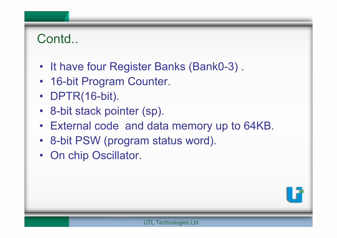
Contd..
• It have four Register Banks (Bank0-3) .• 16-bit Program Counter.• DPTR(16-bit).• 8-bit stack pointer (sp).• External code and data memory up to 64KB.• 8-bit PSW (program status word).• On chip Oscillator.

UTL Technologies Ltd
Program Memory Data Memory
Internal
4K 60K GPR & SFR 64K
External Internal External
Memory Distribution

UTL Technologies Ltd
Data Memory
64K BytesExternal
SFR’S DirectAddressing
Only
Direct and IndirectAddressing
00h
80H
7Fh
FFH
Internal
0000H
And
FFFFH
External

UTL Technologies Ltd
RAM Organization
• The 8051 on-chip memorycan be divided into severalbasic areas
– General Purpose Memory.– Bit Addressable memory.– Register Banks.– Special Function Registers
(SFR).

UTL Technologies Ltd
General Purpose RAM• Byte location from 30h to 7Fh (80 bytes) are
reserved for general purpose use• Location 20h to 2Fh can also be us be used
foe general purpose but care must be takenwhen using these locations for generalpurpose.
• Can be accessed using direct and Indirectaddressing mode.

UTL Technologies Ltd
Register Banks• There are four banks (0-3) from 00h to 1fh.• Each bank has eight registers R0 to R7.• At a time only one bank is used.• By default we can access Bank 0.

UTL Technologies Ltd
R4- Bank 3R5- Bank 3R6- Bank 3R7- Bank 3
R0- Bank 0R1- Bank 0R2- Bank 0R3- Bank 0R4- Bank 0R5- Bank 0R6- Bank 0R7- Bank 0R0- Bank 1R1- Bank 1
Bank 0
Bank 1
Bank 2
Bank 3
Contd,…

UTL Technologies Ltd
Stacks in 8051• Stack is a section of RAM used by the
CPU to store the data temporarily.• SP (Stack Pointer) is the register which
points to the starting position of thestack, default value 07h.
• First location which we can access is08h.
• Storing the data on to stack is calledPUSH and reverse is POP.

UTL Technologies Ltd
Program Status Word
C AC F0 RS1 RS0 OV USR P
PSW.0PSW.1PSW.2PSW.4PSW.5PSW.6PSW.7 PSW.3
•C -Carry Flag
•AC -Auxiliary carry flag
•F0 -General Purpose flag
•RS1 -Register Bank Selector 1
•RS0 - Register Bank Selector 0
•OV -Overflow
•USR -User Defined flag
•P -Parity

UTL Technologies Ltd
PCON• Power Control Register
• SMOD Double baud rate bit.• — Not implemented, reserved for future use.• — Not implemented, reserved for future use.• — Not implemented, reserved for future use.• GF1 General purpose flag bit.• GFO General purpose flag bit.• PD Power Down bit. Setting this bit activates Power
Down operation in the 80C51BH.(Available only inCHMOS).
• IDL Idle Mode bit. (Availableonlyin CHMOS).

UTL Technologies Ltd
Power Down Mode• In the Power Down mode, the on-chip
oscillator is stopped.• On-chip RAM and Special Function Registers
are held.• The port pins output the values held by their
respective SFRS.• ALE and PSEN output will be low.• To come down from power down mode
hardware reset must be used.

UTL Technologies Ltd
Idle Mode• In the Idle mode, the internal clock signal is
gated off to the CPU, but not to the Interrupt,Timer, and Serial Port functions.
• Stack Pointer, Program Counter ,PSW,Accumulator, and all other registers maintaintheir data during Idle.
• The port pins hold the logical status they had atthe time Idle was activated.
• ALE and PSEN hold at logic high levels.

UTL Technologies Ltd
• There are two ways to terminate the Idle.
• Activation of any enabled interrupt will causePCON.O to be cleared by hardware terminated theIdle mode.
• After Servicing the interrupt and following RETI thenext instruction to be executed will be the onefollowing the instruction that put the device into Idle.
• The other way of terminating the Idle mode is withhardware reset.

UTL Technologies Ltd
Idle and Power down mode

UTL Technologies Ltd
Selecting Register Banks• Register bank is selected by configuring the
bits 3 and 4 of the PSW.
RS1 RS0 BANK0 0 00 1 11 0 21 1 3

UTL Technologies Ltd
SFR (Special Function Register)•Locations 80h to FF h are reserved forcontrol, status and I/O control registers.
•Only 21 locations, of the 128 totaladdresses, are used in the 8051 design.
•It has WIDTH OF 8t has WIDTH OF 8--bits.bits.
••A,B,IE,IP,SCON,TCON,P0,P1,P2,P3,PSWA,B,IE,IP,SCON,TCON,P0,P1,P2,P3,PSWare the bit as well as byte addressableare the bit as well as byte addressableregisters.registers.
••PCON,TMOD,DPH,DPL,TL0,TL1,TH0,TH1PCON,TMOD,DPH,DPL,TL0,TL1,TH0,TH1are the byte addressable.are the byte addressable.
••TCON,PCON,SCON,TMOD ,IE,IP are theTCON,PCON,SCON,TMOD ,IE,IP are thecontrol registers.control registers.

UTL Technologies Ltd
PIN Configuration
1234567891011121314151617181920
4039383736353433323130292827262524232221
VCCP0.0 (AD0)P0.1 (AD1)P0.2 (AD2)P0.3 (AD3)P0.4 (AD4)P0.5 (AD5)P0.6 (AD6)P0.7 (AD7)EA/VPPALE/PROGPSENP2.7 (A15)P2.6 (A14)P2.5 (A13)P2.4 (A12)P2.3 (A11)P2.2 (A10)P2.1 (A9)P2.0 (A8)
P1.0P1.1P1.2P1.3P1.4P1.5P1.6P1.7RST
(RXD) P3.0(TXD) P3.1(INT0) P3.2(INT1) P3.3
(T0) P3.4(T1) P3.5
(WR) P3.6(RD) P3.7
XTAL2XTAL1
GND
8051

UTL Technologies Ltd
Pin Description• VCC -Supply voltage.
• GND- Ground.
• RST -Reset input.– A high on this pin for two machine cycles
while the oscillator is running resets thedevice.

UTL Technologies Ltd
• Port 0– Port 0 is an 8-bit open drain bidirectional I/O port.– When 1s are written to port 0 pins, the pins can
be used as high impedance inputs.– Port 0 may also be configured to be the
multiplexed low order address/data bus duringaccesses to external program and data memory.
– In this mode P0 has internal pullups.– Port 0 also receives the code bytes during Flash
programming, and outputs the code bytes duringprogram verification.
– External pullups are required during programverification.

UTL Technologies Ltd
• Port 1– Port 1 is an 8-bit bidirectional I/O port with
internal pullups .– When 1s are written to Port 1 pins they
are pulled high by the internal pullups andcan be used as inputs.
– It also receives the low-order addressbytes during Flash programming andverification.
•

UTL Technologies Ltd
• Port 2– Port 2 is an 8-bit bidirectional I/O port with internal pullups.– When 1s are written to Port 2 pins they are pulled high by
the internal pullups and can be used as inputs.– Port 2 emits the high-order address byte during fetches
from external program memory and during accesses toexternal data memory that use 16-bit addresses (MOVX@DPTR).
– During accesses to external data memory that use 8-bitaddresses (MOVX @ RI), Port 2 emits the contents of theP2 Special Function Register.
– Port 2 also receives the high-order address bits and somecontrol signals during Flash programming and verification.

UTL Technologies Ltd
• Port 3– Port 3 is an 8-bit bidirectional I/O port with
internal pullups.– When 1s are written to Port 3 pins they are
pulled high by the internal pullups and canbe used as inputs.
– Port 3 also receives some control signalsfor Flash programming and verification.

UTL Technologies Ltd
P3.0 RXD (serial input port)P3.1 TXD (serial output port)P3.2 INT0 (external interrupt 0)P3.3 INT1 (external interrupt 1)P3.4 T0 (timer 0 external input)P3.5 T1 (timer 1 external input)P3.6 WR (external data memory write strobe)P3.7 RD (external data memory read strobe)
Port 3 Features
UTL Technologies Ltd
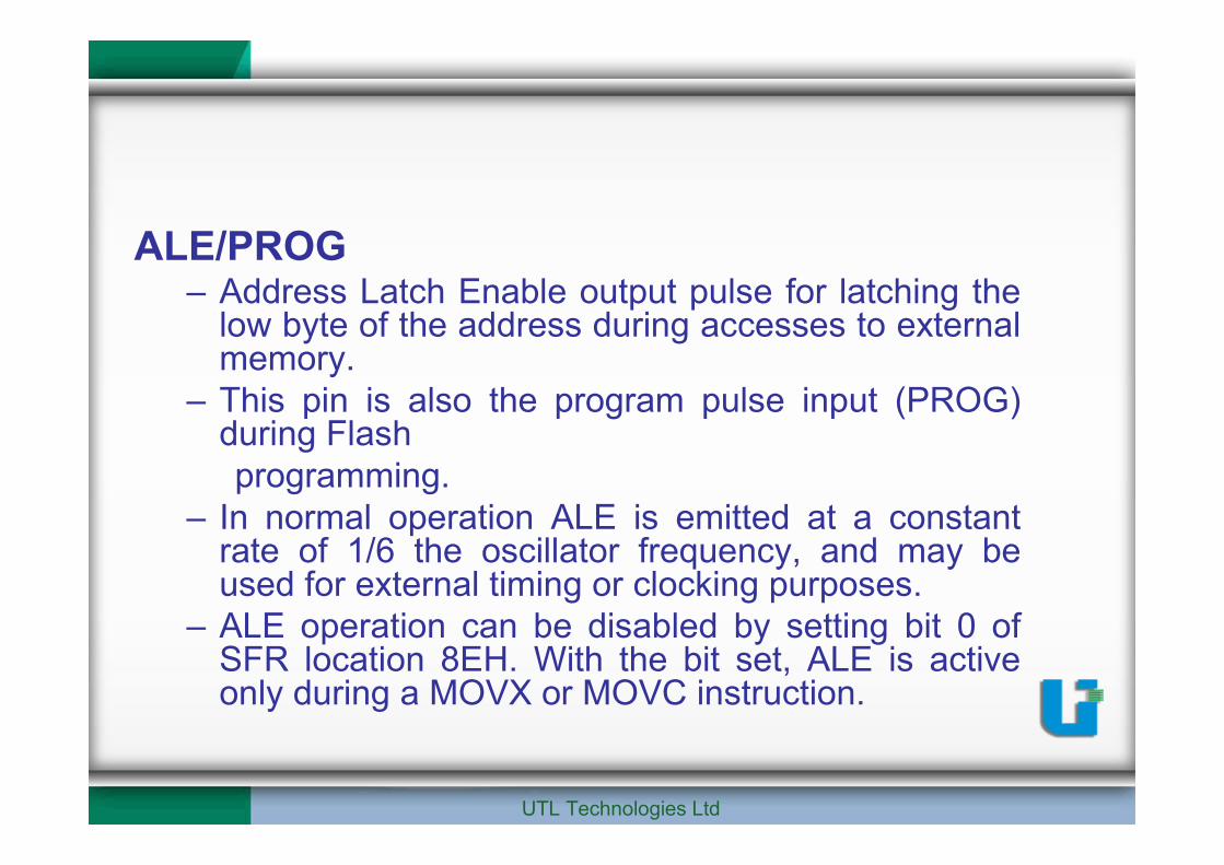
ALE/PROG– Address Latch Enable output pulse for latching the
low byte of the address during accesses to externalmemory.
– This pin is also the program pulse input (PROG)during Flashprogramming.
– In normal operation ALE is emitted at a constantrate of 1/6 the oscillator frequency, and may beused for external timing or clocking purposes.
– ALE operation can be disabled by setting bit 0 ofSFR location 8EH. With the bit set, ALE is activeonly during a MOVX or MOVC instruction.

UTL Technologies Ltd
PSEN– Program Store Enable is the read strobe
to external program memory.– When the AT89C51 is executing code
from external program memory, PSEN isactivated twice each machine cycle,except that two PSEN activations areskipped during each access to externaldata memory.

UTL Technologies Ltd
EA/VPP -External Access Enable.– EA must be strapped to GND in order to enable
the device to fetch code from external programmemory locations starting at 0000H up to FFFFH.
– Note, however, that if lock bit 1 is programmed,EA will be internally latched on reset.
– EA should be strapped to VCC for internalprogram executions.
– This pin also receives the 12-volt programmingenable voltage (VPP) during Flash programming,for parts that require 12-volt VPP.

UTL Technologies Ltd
XTAL1– Input to the inverting oscillator amplifier and
input to the internal clock operating circuit.XTAL2
– Output from the inverting oscillator amplifier.

UTL Technologies Ltd
CPU Timings• All MCS-51 microcontrollers have an on-chip
oscillator which can be used if desired as theclock source for the CPU.
• To use the on-chip oscillator, connect acrystal or ceramic resonator between theXTAL1 and XTAL2 pins of themicrocontroller, and capacitors to ground as
• shown in Power On Reset Circuit.

UTL Technologies Ltd
Power on Reset
C1=C2=33PF,
CRYSTAL=11.0592 MHz

UTL Technologies Ltd
Machine Cycle• A machine cycle consists of a sequence of 6
states, numbered S1 through S6.• Each state time lasts for two oscillator
periods.• Thus a machine cycle takes 12 Oscillator
periods or 1 µs if the oscillator frequency is12 MHz.
• Each state is divided into a Phase 1 half anda Phase 2 half.

UTL Technologies Ltd
Machine Cycle

UTL Technologies Ltd
DC CHARECTERISTICS

UTL Technologies Ltd
AC CHARECTERISTICS

UTL Technologies Ltd
Addressing Modes

UTL Technologies Ltd
Addressing modes
• The data could be in a register, or inmemory, or be provided as animmediate value.
• These various ways of accessing dataare called addressing modes .

UTL Technologies Ltd
Types of Addressing Modes• Immediate Addressing.• Direct Addressing.• Register Addressing.• Indirect Register Addressing.• Indexed Addressing.

UTL Technologies Ltd
Immediate Addressing Mode• In this addressing modes, source
operand is constant. When the instructionis assembled, the operand comesimmediately after the opcode . Theimmediate data must preceded by pounddata”#”.
• Example:– MOV A,#25H ; load 25h into A.
UTL Technologies Ltd
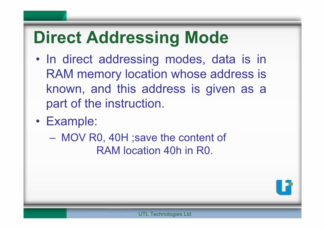
Direct Addressing Mode• In direct addressing modes, data is in
RAM memory location whose address isknown, and this address is given as apart of the instruction.
• Example:– MOV R0, 40H ;save the content of
RAM location 40h in R0.

UTL Technologies Ltd
Register Indirect Addressing Mode• In the register indirect addressing mode,
a register is used as pointer to data.• Example:
– MOV A,@R0 ;move contents of RAMlocation whose address isheld by R0 into A.

UTL Technologies Ltd
Cont….• If the data is inside the CPU, only
registers R0 and R1 are used for thispurpose.
• When R0 and R1 are used for thispurpose , they must be preceded by the“@” sign.

UTL Technologies Ltd
Indexed Addressing Mode• Indexed addressing mode is used to
retrieve data in ROM [code memory]memory location.
• 16-bit register DPTR and register A areused to form the address of the dataelements stored in on chip ROM.
• Example :– MOVC A,@(A+DPTR)

UTL Technologies Ltd
Register Addressing Mode• Register addressing modes involves the
use of registers to hold the data to bemanipulated.
• Examples:– MOV A, RN ; copy the content of Rn into A.– MOV RN, A ;copy the content of A into Rn.

UTL Technologies Ltd
Intro to ALP• An Assembly language program consist
of series of assembly languageinstructions.
• An assembly language instructionconsists of mnemonic ,followed by oneor two operands.
• The Operands are data items beingmanupulated and mnenmonic are thecommands to the CPU.

UTL Technologies Ltd
Example• ORG 0000h• MOV A,#20h• MOV R4,#34h• END.
• ORG and END are the directives to theassembler.
• ORG tells the assembler to place the code atmemory location 0 while END indicates endof the source code.

UTL Technologies Ltd
• An assembly language program consist offour fields.
• [Label:] mnemonic [operand] [;comments].• Brackets indicates field is optional and it
should not be typed in.

UTL Technologies Ltd
Assembling and Running ProgramEditor Program
Assembler
Linker
OH Program
myfile.asm
myfile.lstother obj files
myfile.abs
myfile.hex

UTL Technologies Ltd
• asm or src file is also called as source file.• lst file lists all the opcode , addresses and
errors that assembler detects.• Linker takes one or more object files and
produces as absolute object file with theextension abs.
• abs file is fed into a program called OH( objectto hex converter) and creates a “hex” file that isready to burn into ROM
UTL Technologies Ltd
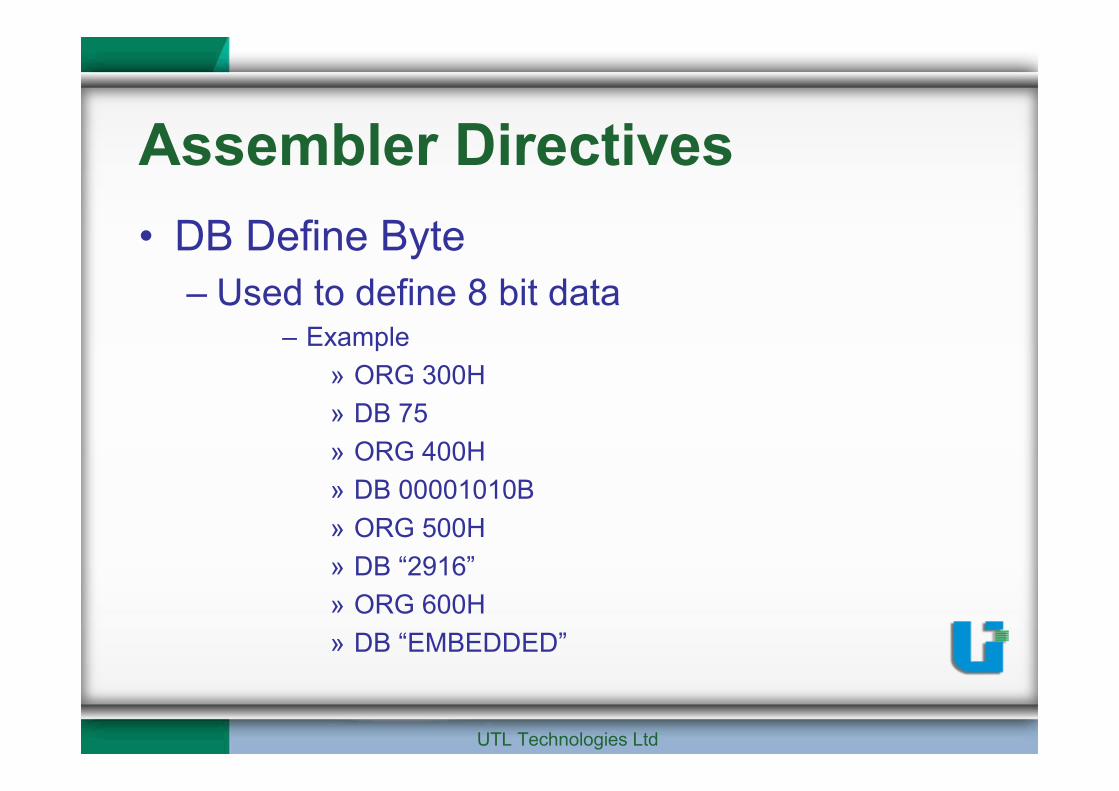
Assembler Directives• DB Define Byte
– Used to define 8 bit data– Example
» ORG 300H» DB 75» ORG 400H» DB 00001010B» ORG 500H» DB “2916”» ORG 600H» DB “EMBEDDED”

UTL Technologies Ltd
Contd,..
• ORG ORIGIN– Used to indicate the starting address of the
program.– Example
» ORG 000H
• EQU EQUATE– Used to define a constant without occupying the
memory location.– Associates a constant with the data label when a
label appears in the program.– Example
» COUNT EQU 92» 2» MOV A,# 9

UTL Technologies Ltd
• END– Indicates to the assembler the end of the
source file
UTL Technologies Ltd
Instruction Set

UTL Technologies Ltd
• Syntax:– opcode dest, source ;
• Source can be a content of memory location,register or an immediate value.

UTL Technologies Ltd
Types of Instruction Sets• Arithmetic Instructions.• Logical Instructions.• Single Bit Instructions.• Data Transfer Instructions.• Branch Instructions.

UTL Technologies Ltd
Arithmetic InstructionsArithmetic Instructions•There are 24 arithmetic instructions which are groupedinto the following types:
¯ADD and ADDC¯SUBB¯MUL¯DIV¯INC¯DEC¯DA

UTL Technologies Ltd
Arithmetic Instuctions
– ADD A,#05h;– SUBB A,SOURCE;– MUL AB;– DIV AB;– INC A– DEC A– DA A

UTL Technologies Ltd
• Flag is a 1-bit register that indicates the statusof the result from an operation
• Flags are either at a flag-state of value 0 or 1
• Arithmetic flags indicate the status of theresults from mathematical operations.
Arithmetic FlagsArithmetic Flags

UTL Technologies Ltd
Arithmetic FlagsArithmetic Flags contd,..contd,..
• There are 4 arithmetic flags in the8051.– Carry Flag -C.– Auxiliary Carry -AC.– Overflow -OV.– Parity -P.

UTL Technologies Ltd
Arithmetic FlagsArithmetic Flags contd,..contd,..
• The C flag is keeping track in unsignedoperation and OV flag is keeping trackin signed operation.

UTL Technologies Ltd
Instructions Affecting FlagsInstructions Affecting FlagsInstruction Mnemonic Flags AffectedADD C AC OVADDC C AC OVSUBB C AC OVMUL C = 0 OVDIV C = 0 OVDA A CSETB C C = 1MOV C, bit C

UTL Technologies Ltd
Instructions Affecting FlagsInstructions Affecting FlagsInstruction Mnemonic Flags Affected
ORL C, bit C
ANL C, bit C
RLC C
RRC C
CLR C C = 0
CPL C C = /C
CJNE C

UTL Technologies Ltd
• ADD A, source ; A = A + source• ADDC A, source ; A = A + source + C .• The C flag is set to 1 if there is a carry out of bit 7• The AC flag is set to 1 if there is a carry out of bit
3.• ADD is used for ordinary addition• ADDC is used to add a carry after the LSB
addition in a multi-byte processNote: A register must be involved in additions
ADD and ADDC InstructionsADD and ADDC Instructions

UTL Technologies Ltd
ExampleExample•Show how the flag register is affectedby the following instructions.
MOV A, #0F5h ; A = F5hADD A, #0Bh ; A = F5 + 0B = 00.

UTL Technologies Ltd
Solution: F5h 1111 0101
+0Bh 0000 1011
100h 0000 0000
After addition register A contains 00h and theflags that are affected are
•CY = 1 since there is a carry out from D7.• P = 0 because the number of 1s is zero.•AC = 1 since there is a carry from D3 toD4.

UTL Technologies Ltd
ExampleExample•Assume that RAM locations 40h – 42h have thefollowing values. Write a program to find the sum ofthe values in these locations. At the end of theprogram, register A should contain the low byte andR7 contain the high byte.
RAM locations: 40h = (7Dh),
41h = (EBh),
42h = (C5h)
UTL Technologies Ltd
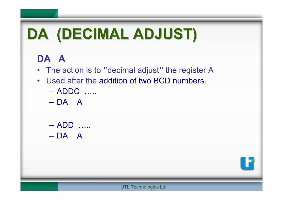
DA A• The action is to “decimal adjust” the register A• Used after the addition of two BCD numbers.
– ADDC …..– DA A
– ADD …..– DA A
DA (DECIMAL ADJUST)DA (DECIMAL ADJUST)

UTL Technologies Ltd
Example for DAExample for DAMOV A,#47h ; A=47h first BCD operand :MOV B, #25h ; B=25h second BCD operandADD A , B ; hex (binary) addition(A=6Ch)DA A ; adjust for BCD addition(A=72h).
-If we add two BCD numbers the resultmust be BCD. Adding 47 to 25 will result into6C which is not BCD. So we must use DAInstruction.

UTL Technologies Ltd
Example for DA InstructionExample for DA Instruction
Offset decimal 6 !
Hex BCD47 0100 0111
+ 25 + 0010 01016C 0110 1100
+ 6 + 011072 0111 0010

UTL Technologies Ltd
• SUBB A, #data• SUBB A, direct• SUBB A, @Ri , where i =0 or 1• SUBB A, Rn, where n =0,1,,7
SUBBSUBB

UTL Technologies Ltd
• SUBB A, source
• No borrow: A = A – source.
• With borrow: A = A – source – carry (i.e.borrow).
• Note that the 8051 uses the 2’s complementmethod to do subtraction.

UTL Technologies Ltd
MUL AB• Uses registers A and B as both source and
destination registers
• Numbers in A and B are multiplied, then putthe lower-order byte of the product in A andthe high-order byte in B.
• The OV flag is set to 1 if the product isgreater than FFh.
• C flag is set all the times.
MULMUL

UTL Technologies Ltd
DIV AB• It uses registers A and B as both source and
destination registers
• The number in A is divided by B.
• The quotient is put in A and the remainder (ifany) is put in B.
• The OV flag is set to 1 if B has the number 00h(divide-by-zero error)
• Note that the C flag is 0 at all times.
DIVDIV

UTL Technologies Ltd
• INC A• INC direct• INC @Ri where i=0,or 1• INC Rn where n=0,,7• To increment (INC) or decrement (DEC)
the internal memory location specified bythe operand.
INC and DECINC and DEC

UTL Technologies Ltd
INC and DECINC and DEC contd,contd,……..• No change with all the arithmetic flags in
this operation.
• Example:• INC 7Fh ; content in 7Fh increased by 1• DEC R1 ; content in R1 decreased by 1

UTL Technologies Ltd
• Logical operations.
• Rotate and swap operations.
• Comparison operations.
Logic Operation in 8051Logic Operation in 8051

UTL Technologies Ltd
General Logic FunctionsGeneral Logic Functions•There are instructions available for the 8051 toimplement the following logic functions.•The source operand can be any of the 4addressing modes (i.e. immediate/register/direct/indirect).
-AND-OR-XOR (exclusive-OR)-NOT (invert/complement)

UTL Technologies Ltd
• ANL destination, sourceDestination = destination AND source.
• ANL direct, A• ANL direct, #data• ANL A, #data• ANL A, direct• ANL A, @Ri where i=0,or 1• ANL A, Rn where n=0,,7• ANL can be used to clear (0) certain bits
Logical ANDLogical AND

UTL Technologies Ltd
Logical ORLogical OR
• ORL destination, sourceDestination = destination OR source.
• ORL can be used to set (1) certain bits.

UTL Technologies Ltd
Logcial XRL• XRL destination, sourceDestination = Destination XOR Source
• Usually, the destination is register A ora direct address in the internal RAM.

UTL Technologies Ltd
CLR A• All bits in register A are cleared.CPL A• All bits in register A are complemented
(inverted)Note :CLR and CPL instructions operate on
register A only
CLR and CPLCLR and CPL

UTL Technologies Ltd
RL A Rotate one bit leftRR A. Rotate one bit rightRLC A Rotate one bit left with carryRRC A Rotate one bit right with carry
• Contents in register A is rotated one bitposition to the left or to the right (operated in Aonly).
• May include the C flag in the operation.
Rotate InstructionsRotate Instructions

UTL Technologies Ltd
01234567
RL A
01234567C
RLC ACarry Flag
01234567
RR A
Before: 10011100After: 00111001
C01234567
Carry FlagRRC A
Before: 10011100 CY = 0After: 00111000 CY = 1
Before: 10011100After: 01001110
Before: 10011100 CY = 1After: 11001110 CY = 0
The Rotate InstructionsThe Rotate Instructions

UTL Technologies Ltd
• Swapping the lower-nibble (lower 4 bits) and thehigher-nibble (upper 4 bits) of register A.
• Register A = 5Eh (original value) after SWAPRegister A = E5h
SWAPSWAP
017 6 5 4 3 2
High Nibble Low Nibble
SWAP A

UTL Technologies Ltd
CJNE destination, source, relative address• Compare the source and destination
operands first then Jump to the relativeaddress (subroutine) if they are notequal .
• Carry flag = 1, if destination-byte is lessthan the source-byte, Otherwise, thecarry flag is cleared.
Comparison OperationComparison Operation
UTL Technologies Ltd
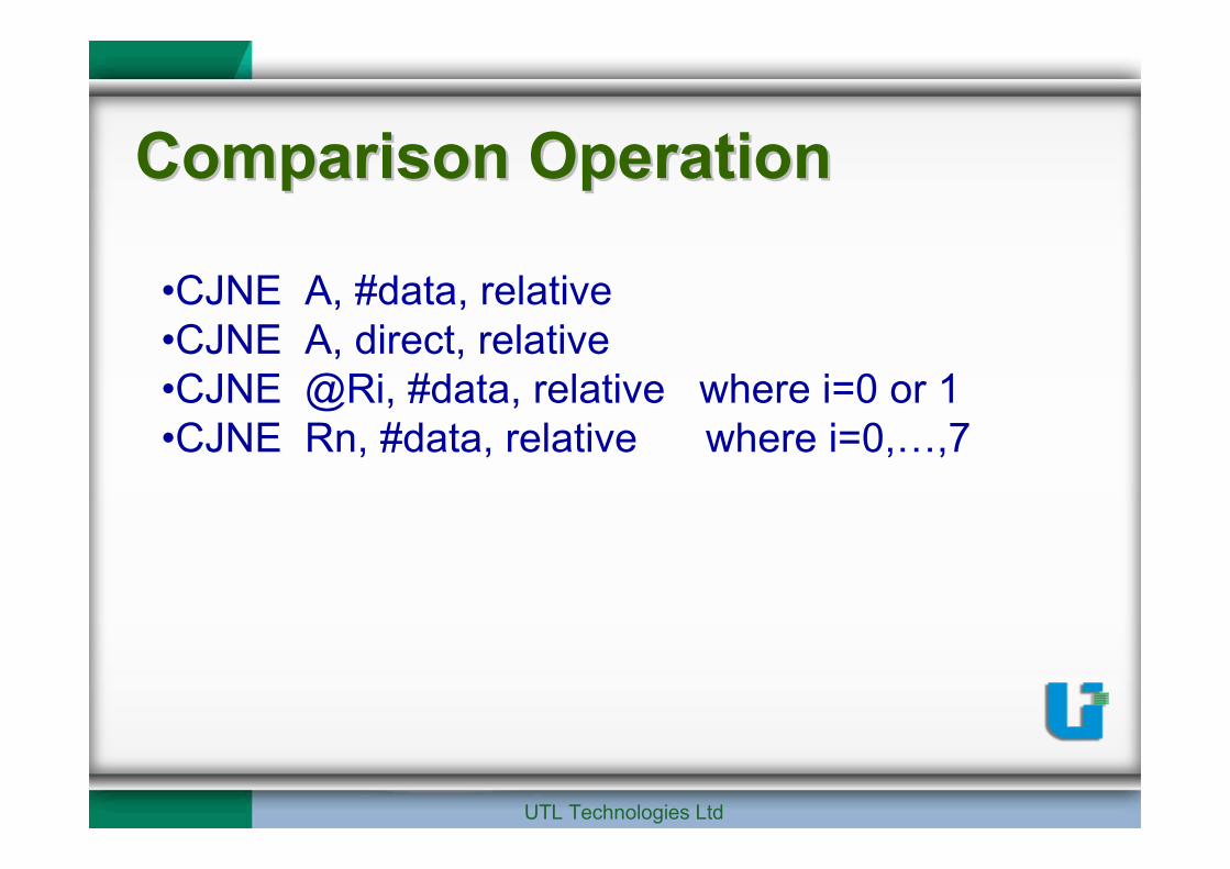
Comparison OperationComparison Operation
•CJNE A, #data, relative•CJNE A, direct, relative•CJNE @Ri, #data, relative where i=0 or 1•CJNE Rn, #data, relative where i=0,…,7
UTL Technologies Ltd
ExampleExample• Write a program segment to monitor P1
continuously for the value of 63h. Itshould get out of the monitoring only ifP1 = 63h.

UTL Technologies Ltd
SolutionSolution
MOV P1, #0FFh ; make P1 an input portHERE :MOV A, P1 ; get P1
CJNE A, #63h, HERE ; keep monitoring unless;P1=63h

UTL Technologies Ltd
Single Bit Instructions• SETB Bit;• CLR Bit;• CPL Bit;• JB Bit,Target• JNB Bit,Target• JBC Bit,Target

UTL Technologies Ltd
Data Transfer Instructions• MOV Source,Dest;• MOVX Source,Dest;• MOVC Source,Dest;

UTL Technologies Ltd
RET and RETI• RET
– Return from a subroutine.• RETI
– Return from a interrupt.
UTL Technologies Ltd
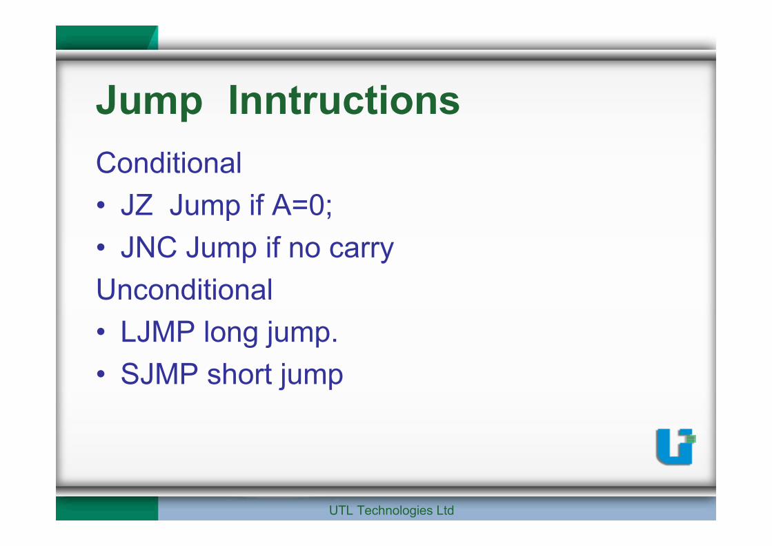
Jump InntructionsConditional• JZ Jump if A=0;• JNC Jump if no carryUnconditional• LJMP long jump.• SJMP short jump

UTL Technologies Ltd
CALL Instructions• LCALL Long call.
– It is 3 byte instruction, first byte is the opcode andsecond and third bytes are used for the targetaddress from subroutine
• ACALL Absolute call.– ACALL is a 2 byte instruction, first byte is opcode
and second byte is used for the target. So targetaddress must be within the 2k bytes.

UTL Technologies Ltd
• PUSH.– Used to move the content of register onto
stack• POP.
– Used to move the content of stack back toregister.

UTL Technologies Ltd
AVR MicrocontrollerADVANCED VIRTUAL RISC

UTL Technologies Ltd
• The AVR is a Harvard architecture machinewith programs and data stored separately.
• Typical Harvard type machines store theirprograms in permanent or semi-permanentmemory and data in volatile memory.
• Hence, they are ideal for embedded systemsin the field, since the program memory isprotected from voltage spikes and otherharsh environmental factors that mightcorrupt the program.

UTL Technologies Ltd
Basic Families• AVRs are generally classified into three broad groups:• tinyAVRs
– 1-8 kB program memory– 8-20-pin package– Limited peripheral set
• megaAVRs– 4-256 kB program memory– 28-100-pin package– Extended instruction set (Multiply instructions and instructions for
handling larger program memories)– Extensive peripheral set
• Application specific AVRs– megaAVRs with special features not found on the other members
of the AVR family, such as LCD controller, USB controller,advanced PWM etc.

UTL Technologies Ltd
Features• Multifunction, Bi-directional General Purpose I/O ports with
configurable, built-in pull-up resistors• Multiple Internal Oscillators• Internal, Self-Programmable Instruction Flash Memory up to
256 K– In-System Programmable using ISP, JTAG, or High Voltage
methods– Optional Boot Code Section with Independent Lock Bits for
Protection• On chip debugging (OCD) support through JTAG or debug
WIRE on most devices• Internal Data EEPROM up to 4 kB• Internal SRAM up to 8 K• 8-Bit and 16-Bit Timers
– PWM output (Dead time generator on some devices)– Input capture

UTL Technologies Ltd
• Analog Comparators• 10-Bit A/D Converters, with multiplex of up to
16 channels• A variety of serial interfaces, including
– I²C Compatible Two-Wire Interface (TWI)– Synchronous/Asynchronous Serial Peripherals
(UART/USART) (used with RS-232, RS-485, andmore)
– Serial Peripheral Interface Bus (SPI)– Universal Serial Interface (USI) for Two or Three-
Wire Synchronous Data Transfer

UTL Technologies Ltd
• Brownout Detection• Watchdog Timer (WDT)• Multiple Power-Saving Sleep Modes• Lighting and motor control (PWM Specific) Controller models• CAN Controller Support• USB Controller Support• Proper High-speed hardware & Hub controller with embedded
AVR.• Ethernet Controller Support• LCD Controller Support• Low-voltage Devices Operating Down to 1.8v• Pico Power Devices

UTL Technologies Ltd
Atmel AVR Usage• AVRs have been use in various automotive
applications such as security, safety,powertrain and entertainment systems. Atmelhas recently launched a new publication"Atmel Automotive Compilation" to helpdevelopers with automotive applications.Some current usages are in BMW, Daimler-Chrysler and TRW.
• USB-based AVRs have been used in theMicrosoft Xbox hand controllers. The linkbetween the controllers and Xbox is USB.

UTL Technologies Ltd
PIC Microcontroller
UTL Technologies Ltd
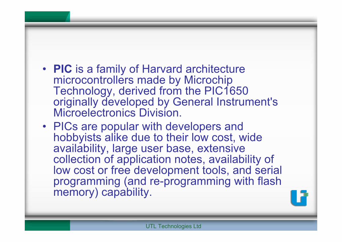
• PIC is a family of Harvard architecturemicrocontrollers made by MicrochipTechnology, derived from the PIC1650originally developed by General Instrument'sMicroelectronics Division.
• PICs are popular with developers andhobbyists alike due to their low cost, wideavailability, large user base, extensivecollection of application notes, availability oflow cost or free development tools, and serialprogramming (and re-programming with flashmemory) capability.

UTL Technologies Ltd
Architecture• The PIC architecture is distinctively minimalist. It is
characterized by the following features:– separate code and data spaces (harvard architecture)– a small number of fixed length instructions– most instructions are single cycle execution (4 clock cycles),
with single delay cycles upon branches and skips– a single accumulator (W), the use of which (as source
operand) is implied (ie is not encoded in the opcode)– All RAM locations function as registers as both source
and/or destination of math and other functions.[1]

UTL Technologies Ltd
– a hardware stack for storing returnaddresses
– a fairly small amount of addressable dataspace (typically 256 bytes), extendedthrough banking
– data space mapped CPU, port, andperipheral registers
– the program counter is also mapped intothe data space and writable (this is used tosynthesize indirect jumps)
UTL Technologies Ltd
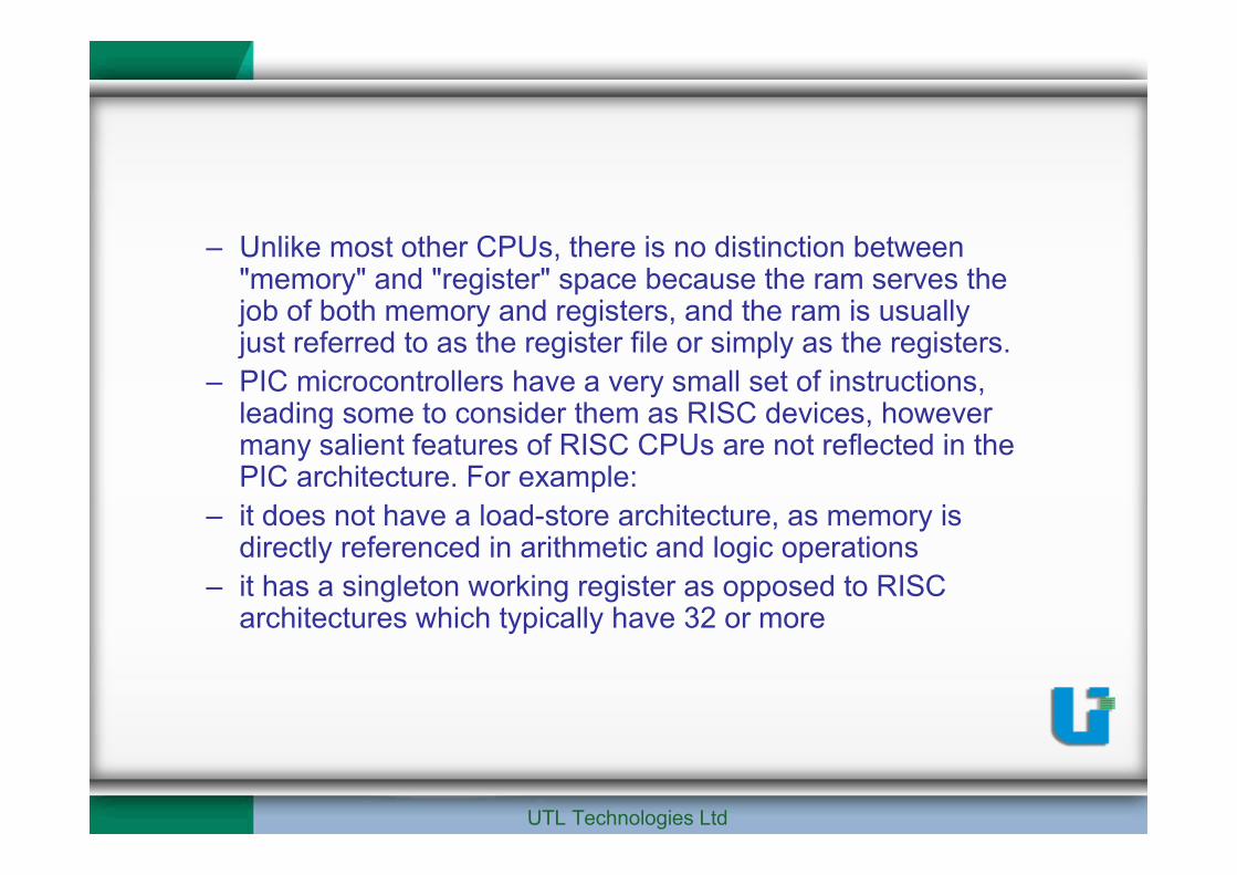
– Unlike most other CPUs, there is no distinction between"memory" and "register" space because the ram serves thejob of both memory and registers, and the ram is usuallyjust referred to as the register file or simply as the registers.
– PIC microcontrollers have a very small set of instructions,leading some to consider them as RISC devices, howevermany salient features of RISC CPUs are not reflected in thePIC architecture. For example:
– it does not have a load-store architecture, as memory isdirectly referenced in arithmetic and logic operations
– it has a singleton working register as opposed to RISCarchitectures which typically have 32 or more

Assignments• Write programs to add, subtract, multiply and
divide two 8 bit numbers• Write programs to add, subtract, multiply and
divide two 16 bit numbers• Increment accumulator contents from 0 to
0xFF• Store 0x56 from locations 0x50 to 0x70 in
internal RAM
UTL Technologies Ltd

• Write a program to clear the internal RAM• Put 5 numbers in the internal memory and
Sort these 5 numbers, in ascending order.• Put 5 numbers in the external memory and
Sort these 5 numbers, in ascending orderand put them back in external memory.
• WAP to move “your name” which is stored atmemory location 300h to the port 1.
UTL Technologies Ltd

• WAP to move the stack to memory location30h and implement PUSH and POP.
• WAP to copy the content of bank 0 to bank 1.• WAP to initialize the bit addressable area to
55h.• WAP to add two numbers and if carry is
generated then set 25h location to 1 else tozero.
UTL Technologies Ltd

• WAP to write a single bit to bit addressablearea of RAM.
• WAP to save accumulator in r7 register ofregister bank 2?
• Subtract a lower number from a highernumber?
• Assuming ram location 40h has a value 97hexchange the lower nibble of a and ramlocation value 40h?
UTL Technologies Ltd

• With out using the XCHD operator. do theabove same problem?
• With out using MUL operator find product oftwo values
•
UTL Technologies Ltd