intrinsic stress effect on fracture toughness of plasma enhanced chemical vapor deposited sinx:h...
TRANSCRIPT

Thin Solid Films 518 (2010) 4898–4907
Contents lists available at ScienceDirect
Thin Solid Films
j ourna l homepage: www.e lsev ie r.com/ locate / ts f
Intrinsic stress effect on fracture toughness of plasma enhanced chemical vapordeposited SiNx:H films
Sean King ⁎, Rosalie Chu, Guanghai Xu, Jennifer HueningLogic Technology Development, Intel Corporation, Hillsboro, OR 97124, United States
⁎ Corresponding author. Tel.: +1 503 613 7547; fax:E-mail address: [email protected] (S. King).
0040-6090/$ – see front matter © 2010 Elsevier B.V. Adoi:10.1016/j.tsf.2010.03.031
a b s t r a c t
a r t i c l e i n f oArticle history:Received 1 April 2008Received in revised form 28 February 2010Accepted 11 March 2010Available online 19 March 2010
Keywords:NanoindentationSilicon nitrideFracture toughnessPlasma CVDStress
The apparent fracture toughness for a series of plasma enhanced chemical vapor deposition SiNx:H films withintrinsic film stress ranging from 300 MPa tensile to 1 GPa compressive was measured using nanoindenta-tion. The nanoindentation results show the measured fracture toughness for these films can vary from ashigh as N8 MPa⋅√m for films in compression to as low as b0.5 MPa⋅√m for the films in tension. Other filmproperties such as density, Young's modulus, and hydrogen content were also measured and not observed tocorrelate as strongly with the measured fracture toughness values. Various theoretical corrections proposedto account for the presence of intrinsic or residual stresses in nanoindent fracture toughness measurementswere evaluated and found to severely underestimate the impact of intrinsic stresses at thicknesses ≤3 μm.However, regression analysis indicated a simple linear correlation between the apparent fracture toughnessand intrinsic film stress. Based on this linear trend, a stress free/intrinsic fracture toughness of 1.8±0.7 MPa⋅√m was determined for the SiNx:H films.
+1 971 214 7811.
ll rights reserved.
© 2010 Elsevier B.V. All rights reserved.
1. Introduction
Fracture toughness is a measure of the resistance to catastrophicmechanical failure that amaterial exhibits in the presence of a crack orother defect. Numerous methods have been employed to experimen-tally measure this mechanical property for brittle materials [1–4] andmany have been adopted and extended for use with thin films [5].However for thin films, one of the most popular methods formeasuring fracture toughness (Kc) has been nanoindentation mea-surements [6–12]. Unlike most other fracture toughness measure-ments, nanoindent Kc measurements do not have strict samplegeometry requirements and are based simply on measuring the sizeand length of cracks induced during indentation. A variety of differentstyles of nanoindenters and crack analysis techniques have been usedto determine the fracture toughness of numerous materials with greatsuccess [5]. However, these measurements have been plagued by highvariability in the reported values (up to 40% [6,13,14]), and in somecases the suitability of the technique as an acceptable fracturetoughness test has been questioned [15]. The high variability hasbeen attributed to the difficulty encountered in measuring the cracklength generated by indentation, detecting the onset of crackformation, and separating out the energy released by crack formationfrom elastic–plastic deformation [8,9]. For thin films, a furtherhindrance of this technique is accounting for the impact of intrinsic
stresses present within the film being tested. The presence of intrinsicstresses in thin films deposited on substrates is ubiquitous and hasmultiple origins including differences in thermal expansion coeffi-cients between film and substrate, lattice constant mismatch,formation of non-equilibrium bond configurations during deposition,structural reorganization/recrystallization processes, chemical reac-tions, and surface implantation of atoms [16]. Unfortunately, thepresence of intrinsic film stresses is not consistently considered innanoindentation fracture toughness measurements of thin films [7,9–11,17–20].
Essentially all nanoindent thin film Kc measurements rely onindentation fracture mechanics analysis originally derived for Kc
measurements of bulk ceramics [21–32]. Many of these analyses donot explicitly account for the possibility of significant residual orintrinsic stresses being present in the material prior to indentation[21–26]. In cases where these bulk material analyses have beenapplied to thin film nanoindentation experiments, the presence ofintrinsic film stresses is ignored or assumed to have a negligibleimpact on the measurements [9–11,33]. When attempts are made toaccount for pre-existing intrinsic or residual stresses in nanoindent Kc
measurements, purely linear elastic deformations are assumed tooccur [27–32]. This allows the principle of superposition to be appliedand additional stress intensity factor (K) terms to be summed [34].The stress intensity terms arising from intrinsic or residual stressesare assumed to have a form of K=ψσ√c where ψ is a constant/stressamplitude factor computed by elasticity theory for bulk materials intension, and c is the crack or defect length [34]. For thin films, thestress intensity factor arising from the presence of intrinsic stresses is
4899S. King et al. / Thin Solid Films 518 (2010) 4898–4907
assumed to have the same form. In some cases, the same stressamplitude factors derived for bulk materials have been applied to thinfilms [12,35–37]. In other cases, intrinsic stresses have beenaccounted for using stress amplitude factors determined from elasticenergy release rate calculations for semi-infinite, steady state channelcracks propagating in thin films in tension [38–41]. However, intrinsicstresses in thin films may be tensile or compressive. For the case ofintrinsic compressive thin film stresses, the correct stress amplitudefactor is not readily apparent. The fact that indentation cracks formedin compressive films are typically not semi-infinite further confusesthe situation. Nevertheless in many cases, the ψ computed for thinfilms in tensile loading have still been used to analyze indentationcrack formation in compressive films [42–44]. Therefore, the validityof applying stress intensity factors computed for tensile loading toanalyze indentation cracks in compressive thin films needs to bedemonstrated.
In this report, we have used nanoindentation to measure thefracture toughness of a series of plasma enhanced chemically vapordeposited (PECVD) SiNx:H thin films. The intrinsic stress of the filmsstudied was intentionally varied from compressive to tensile in orderto assesswhat impact the internal stress has on the fracture toughnessvalues determined by the nanoindentation technique. PECVD SiNx:Hwas selected for this study due to both the well documented ability totune the film stress from compressive to tensile [45–48] and thetechnological importance of these and similar SiCN:H materials to themicroelectronics industry [49–51]. As we will show in this report, thelack of consideration of intrinsic film stresses in nanoindent Kc
measurements can actually make the measured/apparent fracturetoughness significantly higher or lower than the intrinsic fracturetoughness of the material. We additionally show that the stressamplitude factors typically employed to account for the presence ofintrinsic film stresses seriously underestimate the impact of intrinsicfilm stresses on nanoindent Kc measurements for PECVD SiNx:H films.However, we find that the stress free/intrinsic fracture toughness canbe determined based on a simple linear regression analysis of theapparent fracture toughness vs. intrinsic film stress trend.
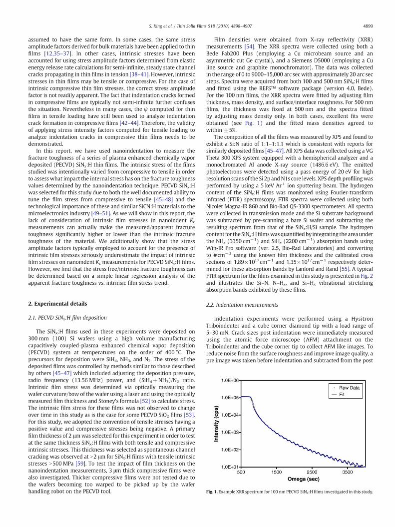
Fig. 1. Example XRR spectrum for 100 nm PECVD SiNx:H films investigated in this study.
2. Experimental details
2.1. PECVD SiNx:H film deposition
The SiNx:H films used in these experiments were deposited on300 mm (100) Si wafers using a high volume manufacturingcapacitively coupled-plasma enhanced chemical vapor deposition(PECVD) system at temperatures on the order of 400 °C. Theprecursors for deposition were SiH4, NH3, and N2. The stress of thedeposited films was controlled by methods similar to those describedby others [45–47] which included adjusting the deposition pressure,radio frequency (13.56 MHz) power, and (SiH4+NH3)/N2 ratio.Intrinsic film stress was determined via optically measuring thewafer curvature/bow of the wafer using a laser and using the opticallymeasured film thickness and Stoney's formula [52] to calculate stress.The intrinsic film stress for these films was not observed to changeover time in this study as is the case for some PECVD SiO2 films [53].For this study, we adopted the convention of tensile stresses having apositive value and compressive stresses being negative. A primaryfilm thickness of 2 μmwas selected for this experiment in order to testat the same thickness SiNx:H films with both tensile and compressiveintrinsic stresses. This thickness was selected as spontaneous channelcracking was observed at N2 μm for SiNx:H films with tensile intrinsicstresses N500 MPa [59]. To test the impact of film thickness on thenanoindentation measurements, 3 μm thick compressive films werealso investigated. Thicker compressive films were not tested due tothe wafers becoming too warped to be picked up by the waferhandling robot on the PECVD tool.
Film densities were obtained from X-ray reflectivity (XRR)measurements [54]. The XRR spectra were collected using both aBede Fab200 Plus (employing a Cu microbeam source and anasymmetric cut Ge crystal), and a Siemens D5000 (employing a Culine source and graphite monochromator). The data was collectedin the range of 0 to 9000–15,000 arc secwith approximately 20 arc secsteps. Spectra were acquired from both 100 and 500 nm SiNx:H filmsand fitted using the REFS™ software package (version 4.0, Bede).For the 100 nm films, the XRR spectra were fitted by adjusting filmthickness, mass density, and surface/interface roughness. For 500 nmfilms, the thickness was fixed at 500 nm and the spectra fittedby adjusting mass density only. In both cases, excellent fits wereobtained (see Fig. 1) and the fitted mass densities agreed towithin ±5%.
The composition of all the films was measured by XPS and found toexhibit a Si:N ratio of 1:1–1:1.1 which is consistent with reports forsimilarly deposited films [45–47]. All XPS data was collected using a VGTheta 300 XPS system equipped with a hemispherical analyzer and amonochromated Al anode X-ray source (1486.6 eV). The emittedphotoelectrons were detected using a pass energy of 20 eV for highresolution scans of the Si 2p andN1s core levels. XPS depth profilingwasperformed by using a 5 keV Ar+ ion sputtering beam. The hydrogencontent of the SiNx:H films was monitored using Fourier-transforminfrared (FTIR) spectroscopy. FTIR spectra were collected using bothNicolet Magna-IR 860 and Bio-Rad QS-3300 spectrometers. All spectrawere collected in transmission mode and the Si substrate backgroundwas subtracted by pre-scanning a bare Si wafer and subtracting theresulting spectrum from that of the SiNx:H/Si sample. The hydrogencontent for theSiNx:Hfilmswasquantifiedby integrating the areaunderthe NHx (3350 cm−1) and SiHx (2200 cm−1) absorption bands usingWin-IR Pro software (ver. 2.5, Bio-Rad Laboratories) and convertingto #cm−3 using the known film thickness and the calibrated crosssections of 1.89×1017cm−1 and 1.35×1017cm−1 respectively deter-mined for these absorption bands by Lanford and Rand [55]. A typicalFTIR spectrum for the films examined in this study is presented in Fig. 2and illustrates the Si–N, N–Hx, and Si–Hx vibrational stretchingabsorption bands exhibited by these films.
2.2. Indentation measurements
Indentation experiments were performed using a HysitronTriboindenter and a cube corner diamond tip with a load range of5–30 mN. Crack sizes post indentation were immediately measuredusing the atomic force microscope (AFM) attachment on theTriboindenter and the cube corner tip to collect AFM like images. Toreduce noise from the surface roughness and improve image quality, apre image was taken before indentation and subtracted from the post
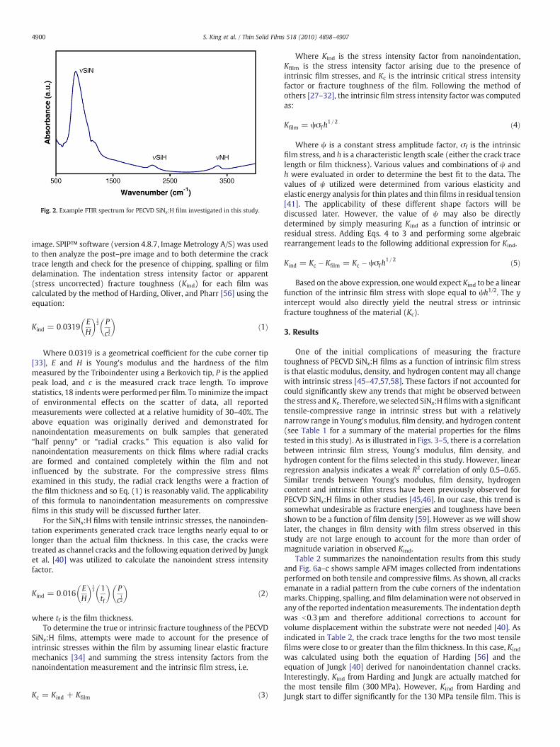
Fig. 2. Example FTIR spectrum for PECVD SiNx:H film investigated in this study.
4900 S. King et al. / Thin Solid Films 518 (2010) 4898–4907
image. SPIP™ software (version 4.8.7, Image Metrology A/S) was usedto then analyze the post–pre image and to both determine the cracktrace length and check for the presence of chipping, spalling or filmdelamination. The indentation stress intensity factor or apparent(stress uncorrected) fracture toughness (Kind) for each film wascalculated by the method of Harding, Oliver, and Pharr [56] using theequation:
Kind = 0:0319EH
� �12 P
c32
� �ð1Þ
Where 0.0319 is a geometrical coefficient for the cube corner tip[33], E and H is Young's modulus and the hardness of the filmmeasured by the Triboindenter using a Berkovich tip, P is the appliedpeak load, and c is the measured crack trace length. To improvestatistics, 18 indents were performed per film. Tominimize the impactof environmental effects on the scatter of data, all reportedmeasurements were collected at a relative humidity of 30–40%. Theabove equation was originally derived and demonstrated fornanoindentation measurements on bulk samples that generated“half penny” or “radial cracks.” This equation is also valid fornanoindentation measurements on thick films where radial cracksare formed and contained completely within the film and notinfluenced by the substrate. For the compressive stress filmsexamined in this study, the radial crack lengths were a fraction ofthe film thickness and so Eq. (1) is reasonably valid. The applicabilityof this formula to nanoindentation measurements on compressivefilms in this study will be discussed further later.
For the SiNx:H films with tensile intrinsic stresses, the nanoinden-tation experiments generated crack trace lengths nearly equal to orlonger than the actual film thickness. In this case, the cracks weretreated as channel cracks and the following equation derived by Jungket al. [40] was utilized to calculate the nanoindent stress intensityfactor.
Kind = 0:016EH
� �13 1
tf
� �P
c12
� �ð2Þ
where tf is the film thickness.To determine the true or intrinsic fracture toughness of the PECVD
SiNx:H films, attempts were made to account for the presence ofintrinsic stresses within the film by assuming linear elastic fracturemechanics [34] and summing the stress intensity factors from thenanoindentation measurement and the intrinsic film stress, i.e.
Kc = Kind + Kfilm ð3Þ
Where Kind is the stress intensity factor from nanoindentation,Kfilm is the stress intensity factor arising due to the presence ofintrinsic film stresses, and Kc is the intrinsic critical stress intensityfactor or fracture toughness of the film. Following the method ofothers [27–32], the intrinsic film stress intensity factor was computedas:
Kfilm = ψσfh1=2 ð4Þ
Where ψ is a constant stress amplitude factor, σf is the intrinsicfilm stress, and h is a characteristic length scale (either the crack tracelength or film thickness). Various values and combinations of ψ andh were evaluated in order to determine the best fit to the data. Thevalues of ψ utilized were determined from various elasticity andelastic energy analysis for thin plates and thin films in residual tension[41]. The applicability of these different shape factors will bediscussed later. However, the value of ψ may also be directlydetermined by simply measuring Kind as a function of intrinsic orresidual stress. Adding Eqs. 4 to 3 and performing some algebraicrearrangement leads to the following additional expression for Kind.
Kind = Kc � Kfilm = Kc � ψσfh1=2 ð5Þ
Based on the above expression, onewould expect Kind to be a linearfunction of the intrinsic film stress with slope equal to ψh1/2. The yintercept would also directly yield the neutral stress or intrinsicfracture toughness of the material (Kc).
3. Results
One of the initial complications of measuring the fracturetoughness of PECVD SiNx:H films as a function of intrinsic film stressis that elastic modulus, density, and hydrogen content may all changewith intrinsic stress [45–47,57,58]. These factors if not accounted forcould significantly skew any trends that might be observed betweenthe stress and Kc. Therefore, we selected SiNx:H filmswith a significanttensile-compressive range in intrinsic stress but with a relativelynarrow range in Young's modulus, film density, and hydrogen content(see Table 1 for a summary of the material properties for the filmstested in this study). As is illustrated in Figs. 3–5, there is a correlationbetween intrinsic film stress, Young's modulus, film density, andhydrogen content for the films selected in this study. However, linearregression analysis indicates a weak R2 correlation of only 0.5–0.65.Similar trends between Young's modulus, film density, hydrogencontent and intrinsic film stress have been previously observed forPECVD SiNx:H films in other studies [45,46]. In our case, this trend issomewhat undesirable as fracture energies and toughness have beenshown to be a function of film density [59]. However as we will showlater, the changes in film density with film stress observed in thisstudy are not large enough to account for the more than order ofmagnitude variation in observed Kind.
Table 2 summarizes the nanoindentation results from this studyand Fig. 6a–c shows sample AFM images collected from indentationsperformed on both tensile and compressive films. As shown, all cracksemanate in a radial pattern from the cube corners of the indentationmarks. Chipping, spalling, and film delamination were not observed inany of the reported indentationmeasurements. The indentation depthwas b0.3 μm and therefore additional corrections to account forvolume displacement within the substrate were not needed [40]. Asindicated in Table 2, the crack trace lengths for the two most tensilefilms were close to or greater than the film thickness. In this case, Kind
was calculated using both the equation of Harding [56] and theequation of Jungk [40] derived for nanoindentation channel cracks.Interestingly, Kind from Harding and Jungk are actually matched forthe most tensile film (300 MPa). However, Kind from Harding andJungk start to differ significantly for the 130 MPa tensile film. This is

Table 1Material properties for films investigated in this study.
Film Film Thick(μm)
Intrinsic stress(MPa)
Young's modulus(GPa)
Hardness(GPa)
Density(g cm−3)
[N–H](1022cm−3)
[Si–H](1022cm−3)
[H](1022cm−3)
SiNx:H #1 1.50a 450±22 100±10 13±1 2±0.1 0.5±0.05 2.0±0.2 2.5±0.2SiNx:H #2 2.00 300±15 155±15 18±2 2.3±0.1 1.1±0.1 1.3±0.1 2.4±0.2SiNx:H #3 2.00 130±7 145±15 17±2 2.4±0.1 0.8±0.1 1.3±0.1 2.1±0.2SiNx:H #4 2.00 60±3 188±19 20±2 2.45±0.1 1.3±0.1 0.8±0.1 2.2±0.2SiNx:H #5 2.00 −100±5 185±18 20±2 2.6±0.1 0.7±0.1 1.4±0.1 2.1±0.2SiNx:H #6 3.00 −100±5 165±16 18±2 2.6±0.1 0.7±0.1 1.4±0.1 2.1±0.2SiNx:H #7 3.00 −270±13 118±12 17±2 2.6±0.1 1.0±0.1 1.2±0.1 2.3±0.2SiNx:H #8 3.00 −480±24 198±20 22±2 2.6±0.1 1.2±0.1 1.0±0.1 2.2±0.2SiNx:H #9 3.00 −650±33 182±18 21±2 2.7±0.1 1.3±0.1 0.9±0.1 2.3±0.2SiNx:H #10 2.00 −650±33 199±19 23±2 2.7±0.1 1.2±0.1 0.9±0.1 2.1±0.2SiNx:H #11 2.00 −650±33 205±20 23±2 2.6±0.1 1.2±0.1 0.8±0.1 2.1±0.2SiNx:H #12 2.00 −950±47 242±24 27±3 2.7±0.1 0.3±0.03 0.6±0.06 1.0±0.1
a Film cracked due to intrinsic stress relief.
4901S. King et al. / Thin Solid Films 518 (2010) 4898–4907
consistent with the fact that the crack trace length for this film is justslightly less than the film thickness and therefore the Jungkexpression is no longer completely valid. The crack trace length/filmthickness ratio was 20–50% for the remainder of the increasinglycompressive films, and use of the Harding expression is thereforereasonably valid. As the Harding equation yielded similar Kind valuesto those of Jungk for clear cases of nanoindent channel cracking and isvalid for the remainder of the films, we will focus on the Hardingvalues for the remainder of this report.
In Fig. 7, we present the nanoindentation stress intensity factor/apparent fracture toughness for the PECVD SiNx:H films vs. theintrinsic film stress. As expected based on Eq. 5, a strong linearcorrelation (R2N0.9) between Kind and film stress is observed withKind steadily decreasing from 7.6±1.3 MPa⋅√m to 0.2±0.1 MPa⋅√mas the compressive film stress decreases from 950±47 MPa to zeroand increases to 300±15 MPa tensile. At this point, we also note thatwe obtained slightly lower values for both E, H and Kind for films of3 μm thickness vs. 2 μm thickness. The E/H ratio, however, is the samefor both 2 and 3 μm films. The differences in Kind between 2 and 3 μmfilms are therefore a result of differences in crack trace lengths. This islikely evidence that some substrate effects are present in our results.The trend between Kind and intrinsic stress is still readily apparentwith linear regression analysis for both the 2 and 3 μm filmsseparately yielding similar values for the slope and the y intercept.For a hypothetical neutral stress film, these linear fits predict acritical stress intensity factor/intrinsic fracture toughness of 1.6±0.25 MPa⋅√m.
Aside from substrate effects which will be discussed more later,the Kind vs. intrinsic stress results may also be impacted by theobserved correlations between film density and elastic modulus.However as shown in Figs. 8 and 9, the correlations between Kind,
Fig. 3. Young's modulus vs. intrinsic film stress for series of PECVD SiNx:H films.
modulus, and film density are not as strong with R2 values of 0.65 foreach case. In an attempt to normalize out the impact of variations inmodulus and density from the Kind results, critical energy release rates(or indentation fracture energy) values were computed from Kind, i.e.Gind=Kind
2 /E. These values are presented in Fig. 10. Linear regressionanalysis still indicates a strong correlation between Gind and intrinsicstress with R2=0.7–0.9.
To determine the true or intrinsic fracture toughness of the PECVDSiNx:H films, we next attempted to compute a separate stressintensity factor directly accounting for the intrinsic stresses withinthe film (prior to indentation) using Eq. 4 (Kfilm=ψσfh
1/2). The valuesof the constant ψwere determined using the elastic energy analysis ofBeuth [41] for the fully cracked film scenario and a similar analysis byYe [60] for the partially cracked film. Both reports provide tabulatedvalues of ψ as a function of the Dundur's parameters α and βwhich arecomputed based on the elastic mismatch between the film and thesubstrate. For comparison purposes and to test various assumptions,Kfilm was computed for both the tensile and the compressive filmsassuming both a fully and partially crack filmed. For the former, hwastaken to be equal to the film thickness, and for the later hwas taken tobe the measured crack trace length. Table 3 summarizes the Dundurand ψ parameters computed for the films in this investigation. Alsosummarized in Table 3 are the values of Kfilm and Kc computedassuming either a fully or partially cracked film.
Fig. 11 graphically illustrates the computed Kc vs. intrinsic filmstress correlation. In this figure, Kc-channel crack is plotted for thosefilms with c/tfN0.9 and Kc-partial crack is plotted for those films withc/tfb0.9. As can be seen, a significant correlation between Kc andintrinsic film stress still exists with R2=0.84 for both 2 and 3 μmfilms. As most of the Kc data was computed using the partial crackstress correction, this would suggest that either ψ or c are being
Fig. 4. Film density vs. intrinsic film stress for a series of PECVD SiNx:H films.

Fig. 5. FTIR hydrogen content vs. intrinsic film stress for a series of PECVD SiNx:H films.
4902 S. King et al. / Thin Solid Films 518 (2010) 4898–4907
underestimated in the intrinsic stress correction. To test the impact ofc on the partial crack intrinsic stress correction, we also computed Kc
for all films using the channel crack intrinsic stress correction as thiswould represent the extreme condition for the partial crack condition.Within the region of ±400 MPa, the Kc computed using the partialand channel crack corrections are roughly the same. At b−400 MPathe two start to diverge as expected due to c/tf decreasing. As shownin Fig. 12, a significant correlation between Kc and intrinsic stress stillexists using even the channel crack correction. This strongly suggeststhat the value of ψ is being underestimated for the partial and channelcrack corrections. However, the slopes for the Kc vs. σf correlationdecreases for both 2 and 3 μm films using the channel crack correctionfor all films. Also, R2 decreased to 0.79 for 2 μm films and dramaticallydecreased further to 0.4 for 3 μm films. This suggests that for the filmthicknesses and c/tf ratios where substrate effects are present (asobserved in this study) h= tf may bemore appropriate for both partialand channel crack scenarios.
Regarding the value of ψ, this parameter alternatively may bedirectly calculated from the slope of Kind vs. σf. From Fig. 7, we haveslopes of −0.004 and −0.003 for 2 and 3 μm films. Taking h to beequal to the film thickness, we determine ψ to be 3.1 and 1.9respectively. These values of ψ are 2–3× higher than those determinedby elasticity theory for 2 μm films and 1.3–1.6X higher for 3 μm films.This demonstrates that use of the Beuth and Ye analysis is not suitablefor nanoindent Kc measurements where the crack/film thicknessratios are≪2 and the assumption of semi-infinite crack lengths is notvalid. This also illustrates the impact that film thickness may have onindentation measurements as the graphically determined values of ψappear to approach those of theoretical analysis as the film thicknessincreases. Alternatively, h can be taken to be the crack trace length. In
Table 2Summary of nanoindentation results for PECVD SiNx:H films investigated in this study.
Film Intrinsic stress(MPa)
Force(mN)
Contact depth(μm)
c — crack length(μm)
c/tf
SiNx:H #1 450 NAa NAa ∞ ∞SiNx:H #2 300 30 b0.3 5.93±0.10 2.97SiNx:H #3 130 30 b0.3 1.80±0.06 0.90SiNx:H #4 60 30 b0.3 1.33±0.14 0.67SiNx:H #5 −100 30 b0.3 1.07±0.11 0.53SiNx:H #6 −100 30 b0.3 1.49±0.25 0.50SiNx:H #7 −270 30 b0.3 1.23±0.15 0.41SiNx:H #8 −480 30 b0.3 0.95±0.08 0.32SiNx:H #9 −650 30 b0.3 0.86±0.10 0.29SiNx:H #10 −650 30 b0.3 0.72±0.08 0.36SiNx:H #11 −650 30 b0.3 0.80±0.08 0.40SiNx:H #12 −950 30 b0.3 0.52±0.07 0.26
a Film cracked due to intrinsic stress relief.NA, not applicable.
this case, the empirically determined values of ψ range from 1.81 up to6.1 as the intrinsic stress changes from 400 MPa tensile to 950 MPacompressive. The differences in ψ determined by elasticity theory andfrom our measurements will be discussed further in the next section.
Fig. 13 shows Kc vs. intrinsic film stress using the values of ψgraphically derived from Fig. 7 and h= tf. As expected, Kc no longershows a significant dependence on stress with R2b0.15 for both filmthicknesses. All data points are bundled around 1.8 MPa⋅√m with anall films average value of 1.8±0.7 MPa⋅√m. This all film averagevalue is consistent with the neutral stress value 1.6±0.25 MPa⋅√mgraphically derived from Fig. 7.
4. Discussion
Before discussing our Kc measurements and trends with filmstress, it is first important to note that the film stresses, elastic moduliand film densities determined for the films used in this study are allconsistent with those reported by others for films prepared in asimilar fashion [45–47,61–64]. As for the Kc/Gc values, we are aware ofonly one recent study in which Kc was reported for a PECVD SiNx:Hfilm. In that study by Hughey and Cook [48], they deduced Kc for acouple of tensile SiNx:H films which were observed to crack above acritical thickness. The values they report range from 0.9 to1.4 MPa⋅√m and are nominally consistent with the Kind values of0.2–2.1 MPa⋅√m observed in our study. We have likewise performeda separate analysis similar to that of Hughey and Cook for some of thetensile SiN films investigated in this study and determined Kc values of1–1.7 MPa⋅√m [65]. Using the method of Hughey and Cook andassuming E=200 GPa, one can also extract Kc data from the crackingvs. thickness data reported by Ulrich et al. for their PECVD SiNx:H films[52]. In this case, a similar range in Kc of 0.14–1.6 MPa⋅√m was alsoobserved.
For further comparison, it would at first seem natural to compareour values against those for Si3N4 ceramics for which a vast body ofliterature reporting on fracture energies and toughness does exist.However, comparison of our measurements for PECVD SiNx:H thinfilms with Si3N4 ceramics would be totally inappropriate for severalreasons. These reasons include the clear differences in crystal struc-ture (amorphous vs. polycrystalline), density (N3.2 vs. b2.8 gm cm−3),stoichiometry (N/Si=1.1 vs. 1.33) and purity (b0.1% impurity vs. 1–5%sintering aids) that exist between PECVD SiNx:H and Si3N4 ceramics.For these reasons, we limit ourselves to only briefly comparing ourresults to those by Tanaka et al. [66] for a pure (no sintering aids), fullydensified, stoichiometric Si3N4 bulk polycrystalline ceramic prepared byhot isostatic press sintering at≥1600 °C. For this Si3N4material, Tanakaet al. report aKc of 3 MPa⋅√m.Although the presence (or lack thereof) ofstresses within the Tanaka material is unknown, this value is clearly
Kind Harding(MPa⋅√m)
Kind min. Harding(MPa⋅√m)
Kind max. Harding(MPa⋅√m)
Kind Jungk(MPa⋅√m)
0a 0a 0a 0a
±0.10 0.2 0.19 0.21 0.2±0.1±0.06 1.3 1.1 1.5 0.4±0.1±0.14 2.1 1.8 2.5 0.4±0.1±0.11 2.9 2.5 3.3±0.25 1.8 1.5 2.3±0.15 1.9 1.5 2.3±0.08 3.1 2.7 3.5±0.10 3.4 2.9 4.1±0.08 4.6 3.8 5.4±0.08 4.0 3.4 4.9±0.07 7.6 6.3 9.5

Fig. 7. Nanoindentation apparent fracture toughness (Kind) vs. intrinsic film stress forPECVD SiNx:H.
Fig. 8. Nanoindentation apparent fracture toughness (Kind) vs. film density for PECVDSiNx:H.
Fig. 6. AFM images of nanoindentationmarks from(a) 650 MPa compressive, (b) 130 MPatensile, and (c) 300 MPa tensile PECVD SiNx:H.
Fig. 9. Nanoindentation fracture toughness (Kind) vs. Young's modulus for PECVDSiNx:H.
4903S. King et al. / Thin Solid Films 518 (2010) 4898–4907
consistent with the Kind values obtained in our study for compressivePECVD SiNx:H films.
Additional comparisons can also be made to theoretical estimatesof the fracture energy for crystalline Si3N4. Using simple bond energycalculations, we have previously calculated the fracture energy for(0001) Si3N4 to be ∼4.4 J/m2 [58]. This value is supported bymolecular dynamic simulations by Kalia et al. [67] which determinedthe fracture energy for crystalline Si3N4 to be 4 J/m2. Taking the elastic
modulus for (0001) β-Si3N4 to be 520 GPa [68], yields a Kc of2 MPa⋅√m. This value is reasonably close to our Kind value of 1.6±0.25 MPa⋅√m for neutral stress PECVD SiNx:H. As we will show later,taking into consideration the differences in densities between thesematerials will bring the Kc into closer agreement.
Considering now the observed trend in Kind with film stress, thereare two plausible explanations. The first explanation is that theobserved trend is just an artifact of E or film density changing inparallel with film stress. As Fig. 3 clearly illustrates, the observedchanges in E cannot be responsible for the observed Kind vs. stresstrend. A simple square root of the ratio of the highest and lowest

Fig. 10. Nanoindentation apparent fracture energy (Gind) vs. intrinsic film stress forPECVD SiNx:H. Fig. 11. Intrinsic fracture toughness (Kc) vs. intrinsic film stress for PECVD SiNx:H
calculated using Kc-channel crack (Kc-CC) for filmswith c/tf N0.9 and Kc-partial crack forfilms with c/tf b0.9.
Fig. 12. Intrinsic fracture toughness (Kc) vs. intrinsic film stress for PECVD SiNx:Hcalculated using fully channel cracked film stress intensity factor for all films.
4904 S. King et al. / Thin Solid Films 518 (2010) 4898–4907
Young's modulus would predict only a (250/100)1/2=1.6 change inKind for the films vs. the observed near two order magnitude invariation. However as Figs. 4 and 8 illustrate, a more significantcorrelation can be observed between film density, film stress, and Kind.Such a trend between density and Kind would be expected based onthe fact that a lower density material would have fewer bonds to bebroken along the crack path and would therefore exhibit a reducedfracture energy or toughness. In a prior report [59], we havedemonstrated that this density effect can be easily accounted for bydetermining the fracture energy of a fully dense crystal (Γcrystal) andthen normalizing that value by the ratio of the density of theamorphous form of the material (ρamor) to the crystalline material(ρcrystal), i.e. Kc=(EΓcrystal(ρamor /ρcrystal))1/2. Doing so, we findthat the density effect would at most change the reported Kc by(2.7/2)1/2=1.16. Combining both the density and modulus variationswould barely amount to a factor of two variations in Kind. This is toosmall to account for the order of magnitude change observed in thisstudy. Clearly, intrinsic film stresses are the primary contributor to theobserved variation in Kind.
With the effect of intrinsic film stress on Kind clearly established,the next matter to discuss is how to accurately account for theseinternal stresses and compute the stress free/intrinsic fracturetoughness of the film — Kc. To correct for the presence of these pre-indentation stresses, we calculated a separate stress intensity factorKfilm based on the intrinsic film stress and then assumed linear elasticfracture mechanics such that Kc=Kind+Kfilm. To compute Kfilm, weadopted the methods of others and took Kfilm to have the formKfilm=ψσf√hwhere ψ was a constant stress amplitude factor and h isa critical dimension typically taken as either the crack length c or thefilm thickness tf. To calculate Kfilm, we utilized values of ψ determinedby elasticity theory for full or partial channel cracks of semi-infinitelength propagating in thin films in residual tension. We found that
Table 3Elastic mismatch/Dundur parameters (α, and β), theoretically calculated values of ψ, Kfilm s
Film Intrinsic stress(MPa)
α β ψ(Channel crack)
ψ(Partial crack)
SiNx:H #1 450±22 −0.24 −0.09 1.30 NASiNx:H #2 300±15 −0.02 −0.02 1.41 NASiNx:H #3 130±7 −0.06 −0.03 1.39 1.73SiNx:H #4 60±3 0.07 0.01 1.44 1.61SiNx:H #5 −100±5 0.06 0.06 1.44 1.34SiNx:H #6 −100±5 0.01 −0.01 1.41 1.28SiNx:H #7 −270±13 −0.16 −0.06 1.33 1.18SiNx:H #8 −480±24 0.10 0.02 1.46 1.05SiNx:H #9 −650±33 0.06 0.00 1.44 1.05SiNx:H #10 −650±33 0.06 0.00 1.44 1.10SiNx:H #11 −650±33 0.11 0.02 1.46 1.22SiNx:H #12 −950±47 0.20 0.05 1.53 1.00
values of Kfilm computed in this manner resulted in Kc values that stillshowed a significant correlation to the intrinsic film stress regardlessof whether h was taken as the crack length or film thickness. Thiscould be a result of the failure of one or more of our assumptions.However, our assumptions of linear elastic fracture mechanics andKfilm=ψσf√h appears to be valid as our observed Kind values areclearly linear functions of σf. This leaves to question only the values ofψ. The application of ψ values determined for films in tensile loadingto those in compressive loading does seem suspect. When one
tress intensity factors, and Kc for the PECVD SiNx:H films investigated in this study.
Kfilm channel crack(MPa⋅√m)
Kfilm partial crack(MPa⋅√m)
Kc-channel crack(MPa⋅√m)
Kc-partial crack(MPa⋅√m)
0.72 NA 0.72 NA0.60 NA 0.80 NA0.26 0.30 1.56 1.600.12 0.11 2.22 2.21
−0.20 −0.14 2.70 2.76−0.24 −0.16 1.56 1.64−0.62 −0.35 1.28 1.55−1.22 −0.49 1.88 2.61−1.62 −0.63 1.78 2.77−1.32 −0.60 3.28 4.00−1.34 −0.71 2.66 3.29−2.05 −0.69 5.55 6.91

Fig. 13. Intrinsic fracture toughness (Kc) vs. intrinsic film stress for PECVD SiNx:Hcalculated using empirically derived intrinsic film stress intensity factors.
Fig. 14. PECVD SiNx:H stress free fracture toughness (Kc) vs. film density.
4905S. King et al. / Thin Solid Films 518 (2010) 4898–4907
considers the assumption of semi-infinite length channel cracks in theaforementioned elasticity analysis, the application of ψ to films withfinite crack lengths also seems questionable.
However, the observed dependence of Kind on film thicknesssuggests that ψ may simply need to be more sensitive to tf thendetermined by elasticity theory in order to account for the presence ofsubstrate effects in cube corner Kind measurements performed on≤∼3 μm films. Despite the relative small elastic mismatch betweenthe PECVD SiNx:H films and the Si substrate in this study, the presenceof film thickness/substrate effects is clearly apparent in both ournanoindentation E, H and Kind measurements. As noted earlier, thesubstrate effects present in our E and H values do not enter into theKind measurements due to Kind being a function of the E/H ratio whichwas found to be the same for 2 and 3 μm films. The Kind film thicknessdependence appears to come from the dependence of the crack tracelength on film thickness. This indicates that the ψ utilized to accountfor intrinsic stresses in nanoindent Kc measurements needs to bemore sensitive to tf than determined by elasticity theory for channelcracks of semi-infinite length. This is supported by the 2–3X largervalues of ψ determined from empirical graphical analysis of our Kind
vs. σf data. Though, the discrepancy observed between the empiricallycalculated values of ψ and those determined by elasticity theory wassmaller for the thicker 3 μm films. This suggests that for sufficientlythick filmswhere substrate effects are not present in Kind, the values ofψ determined from elasticity theory may allow the effect of intrinsicstresses to be accurately accounted for despite the breakdown of someof the assumptions mentioned above. Unfortunately for cases wheresubstrate effects will be present in Kind, it appears that ψ must beempirically determined as in our study, or a more detailednanoindentation analysis accounting for substrate and other effectsis needed [38,39].
After empirically determining the correct values of ψ for the films inthis study via linear regression analysis of the Kind vs. σf data, we wereable to effectively account for the intrinsic film stresses in our Kind
measurements and determine Kc for each film (see Fig. 13). Based on allthefilms, anaverage stress freeKc of 1.8±0.7 MPa⋅√mwasdetermined.This value compares well with the range of 1–1.7 MPa⋅√m previouslydetermined for tensile SiNx:H films based on observations of the criticalthickness for intrinsic stress crackingbybothourselves [65] andHugheyand Cook [48]. This value also compares well with the theoreticalvalue of 2.0 MPa⋅√m for crystalline Si3N4. If one were to reduce thistheoretical value by the square root of the ratio of the density of theseamorphous materials to the crystalline material ((2.5/3.2)1/2), onewould obtain 1.75±0.15 MPa⋅√m which is in even better agreement.Likewise, the density reduced experimental Kc for fully densepolycrystalline Si3N4 also falls within our Kc distribution at 3×(2.5/3.2)1/2)=2.65±0.15 MPa⋅√m. It is also possible that some of the
scatter in our stress free Kc values may be a result of the differences infilm/bonddensity. In fact, onewould expect at least a 2×((2.7/3.2)1/2−(2/3.2)1/2)=0.25 MPa⋅√m range in Kc based on the theoretical Kc forSi3N4 and the range in SiNx:Hfilmdensities in this study. To determine ifthere is still a density effect in our stress free Kc data, we have plotted Kc
vs. film density in Fig. 14. For comparison, we have also included thedensity reduced theoretical Si3N4Kc. As expected, Fig. 14 displays a cleartrend between the experimental stress free Kc and film density that isconsistent with theory. Thus, ±0.15 MPa⋅√m of the variation in ourstress free Kc values can be attributed to variations in the density of ourPECVD SiNx:H films.
As all indentation measurements described in this study wereperformed in laboratory air with a relative humidity of 30–40%, it isalso important tomention the possible impact of ambient moisture onour results. Previous indentation fracture toughness measurementshave clearly shown the ability of ambient moisture to lower thethreshold for cracking of SiO2 and other oxide based materials leadingto lower values of Kc [69]. In addition, the intrinsic stress for PECVDSiO2 films has been observed to change significantly over time due toreaction with ambient moisture [53]. In our case, it is likely that somemoisture related effects are present and leading to reduced values ofKc. However the intrinsic stresses present in our PECVD SiNx:H filmswere observed to be stable over the time frame of the nanoindenta-tion experiments. This implies a lower moisture sensitivity for PECVDSiNx:H relative to PECVD SiO2. Lastly, all films were indented withsimilar levels of background humidity. To the first order, we expectthe impact of this effect to be the same for all films and not impact theoverall trends with intrinsic stress that we have observed.
It is also important to discuss the possibility of defects beingpresent within the SiNx:H films and impacting the Kind measurements.Possible defects could be both macroscopic (particles, voids) andmicro/nanoscopic (inclusions, pores, and strained bonds) in origin.Macroscopic defects are unlikely as all indents were performed wellaway from any visible defects and all films were deposited using ahigh volume manufacturing PECVD tool with defect performancecontrolled to ≤1–2 defectsN0.1 μm added per wafer [65]. Defectssignificantly smaller than this would be 1–10 nm in scale andrepresent a second phase material with different bond angles andcharacteristics from the film. If present in significant quantities,defects of these types should be detectable by FTIR. In Fig. 15, wepresent FTIR spectra for several of the films in this study spanning the450 MPa tensile–950 MPa compressive intrinsic stress range. Fig. 15covers the 600–1400 cm−1 spectral region where the most prevalentSi–N, Si–C, and Si–O absorption bands are present. As can be seen, onlythe Si–N asymmetric and N–H bond bending bands are observed [70].A slight shift in the peak position of the asymmetric Si–N stretch from830 to 850 cm−1 is observed as film stress changes from 450 MPaTensile to 950 MPa compressive which is a direct result of the impact

Fig. 15. FTIR spectra for PECVD SiNx:H films as a function of intrinsic film stress.
4906 S. King et al. / Thin Solid Films 518 (2010) 4898–4907
of intrinsic stress on the vibrational frequency of this bond. Morestructure related changes are observed with the N–H stretch whichbecomes more prominent as film stress decreases from compressiveand becomes tensile. This is indicative of decreased network bondingin the film and is consistent with the decreased film density andincreased hydrogen content in the SiNx:H films as intrinsic stressmoves from compressive to tensile. Thus, we do not feel that there areany defect modes contributing to our Kind results.
Lastly, it is interesting to examine a few cases in which nanoindentfracture toughness values have been reported for similar materialswith significant differences in film stress. In this regard, thenanoindent fracture toughness measurements for diamond likecarbon (DLC) films by Nastasi [18] are particularly interesting. Inthis study, a Kc of 10.3 MPa⋅√mwas determined for a 1.9 μm thick DLCfilm deposited on Si with a modulus of 160 MPa and a compressiveintrinsic stress of 2.49 GPa. Based on separate bond breakagecalculations, they determined that the intrinsic fracture toughnessfor this DLC film should be only 1.5 MPa⋅√m. They attributed thisdifference to plastic work and/or tortuous path crack evolution duringthe indentation fracture process. However based on the results in thisstudy, it is clear that the significant compressive stresses presentwithin the DLC films should have a major effect on the apparentnanoindentation fracture toughness. As the DLC film thickness andfilm/substrate elastic mismatch in the Nastasi study is comparable tothose in our study, it is possible to attempt to correct the apparent DLCKc for the presence of the compressive intrinsic stress utilizing theempirically determined ψ from our study. In doing so, we determine astress free DLC Kc of 0.2±2 MPa⋅√m based on the data for all the DLCfilms reported in the Nastasi study. While there is a large variability inthe calculated Kc, these values are clearly in much better agreementwith the theoretical Kc determined by Nastasi for their DLC films.Utilization of ψ values determined for channel cracks by elasticitytheory would have produced much higher values of Kc on the order of6–8 MPa⋅√m. Recent micro scale fracture beam measurements ontetrahedral amorphous carbon (ta-C) films have indicated a stress freefracture toughness of 3–4 MPa⋅√m for this material. Given themodulus for ta-C is 760 GPa, it is reasonable to expect the stressfree Kc for DLC to be in the b3 MPa⋅√m range [71].
In summary, we feel that we have demonstrated the presence ofintrinsic film stresses can have a profound effect on the values ofapparent fracture toughness determined by thin film nanoindentationmeasurements. We have further demonstrated that typical stressamplitude factors utilized to account for the presence of intrinsic filmstresses severely underestimate the effect of these stresses onnanoindent fracture toughness measurements. In these measure-ments, this appears to be due to a combination of the presence ofsubstrate effects in the Kind measurements and the lack of a suitableelasticity analysis to account for these substrate effects in both Kind
and ψ. We hope these results underscore the need for appropriatetheoretical modeling to account for the presence of intrinsic filmstresses in these measurements and motivate additional studies todevelop refined models for assessing the impact of intrinsic stresseson thin film nanoindent fracture toughness measurements.
5. Conclusions
Nanoindentation was used to measure the fracture toughness of aseries of PECVD SiNx:H films with film stress ranging from 300 MPatensile to 950 MPa compressive. Over this range of film stress, theapparent fracture toughness (Kind) was observed to vary bymore thanan order of magnitude from 0.2 to ∼8.0 MPa⋅√m. Based on strength ofcorrelation, the variation in Kind was concluded to be almost entirelydue to the intrinsic film stress relative to other film properties such asdensity, hydrogen content, and Young's modulus which also varied inthis study. The near linear correlation between Kind and intrinsic filmstress was also found to be consistent with expectations based onassumptions of linear elastic fracture mechanics. However, varioustheoretical corrections proposed to account for the presence ofintrinsic or residual stresses in nanoindent fracture toughnessmeasurements were found to severely underestimate the impact ofintrinsic stresses at thicknesses b3 μm. This was concluded to be aresult of a combination of factors including the presence of substrateeffects in Kind, and underestimating the stress amplitude factor ψutilized to compute the stress intensity factors for intrinsic film stress.Based on our results, wewere able to determine empirical values for ψfrom linear regression analysis of the Kind vs. σf data. Using theseempirical values of ψ, we determined the stress free fracturetoughness (Kc) for PECVD SiNx:H to be 1.8±0.7 MPa⋅√m.
Acknowledgements
The authors wish to thank Drs. Brad Sun of Intel and AndyAntonelli of Novellus Systems for their encouraging and thoughtfuldiscussions.
References
[1] P.P. Gillis, J.J. Gilman, J. Appl. Phys. 35 (1964) 647.[2] A.G. Evans, E.A. Charles, J. Am. Ceram. Soc. 59 (1976) 371.[3] S.D. Conzone, W.R. Blumenthal, J.R. Varner, J. Am. Ceram. Soc. 78 (1995) 2187.[4] G.A. Gogotsi, Ceram. Int. 29 (2003) 777.[5] S. Zhang, D. Sun, Y. Fu, H. Du, Surf. Coat. Technol. 198 (2005) 74.[6] G.M. Pharr, Mat. Sci. Engr. A 253 (1998) 151.[7] A.A. Volinsky, W.W. Gerberich, Microelectron. Eng. 69 (2003) 519.[8] J. Chen, S.J. Bull, Thin Solid Films 494 (2005) 1.[9] M.D. Michel, L.V. Muhlen, C.A. Achete, C.M. Lepienski, Thin Solid Films 496 (2005)
481.[10] X. Li, B. Bhushan, Thin Solid Films 355–356 (1999) 330.[11] P. Jedrzejowski, J.E. Klemberg-Sapieha, L. Martinu, Thin Solid Films 466 (2004)
189.[12] J. Malzbender, G. de With, J.M.J. den Toonder, Thin Solid Films 366 (2000) 139.[13] A.A. Volinsky, J.B. Vella, W.W. Gerberich, Thin Solid Films 429 (2003) 201.[14] J.R. Kelly, M.E. Cohen, J.A. Tesk, J. Am. Ceram. Soc. 76 (1993) 2665.[15] G. Quinn, R. Bradt, J. Am. Ceram. Soc. 90 (2007) 673.[16] M. Ohring, The Materials Science of Thin Films, Academic Press, New York, NY,
1992.[17] P. Kodali, K. Walter, M. Nastasi, Trib. Int. 30 (1997) 591.[18] M. Nastasi, P. Kodali, K. Walter, J. Embury, R. Raj, Y. Nakamura, J. Mater. Res. 14
(1999) 2173.[19] J. Gerretsen, G. Kirchner, T. Kelly, V. Mernagh, R. Koekoek, L. McDonnell, Surf. Coat.
Technol. 60 (1993) 566.[20] P. Jedrzejowski, J. Klemberg, L. Martinu, Thin Solid Films 426 (2003) 150.[21] B. Lawn, M. Swain, J. Mater. Sci. 10 (1975) 113.[22] B. Lawn, R. Wilshaw, J. Mater. Sci. 10 (1975) 1049.[23] B. Lawn, E. Fuller, J. Mater. Sci. 10 (1975) 2016.[24] B.R. Lawn, D.B. Marshall, J. Am. Ceram. Soc. 62 (1979) 347.[25] B.R. Lawn, A.G. Evans, B.R. Lawn, D.B. Marshall, J. Am. Ceram. Soc. 63 (1980) 574.[26] G.R. Anstis, P. Chantikul, B.R. Lawn, D.B. Marshall, J. Am. Ceram. Soc. 64 (1981)
533.[27] D. Marshall, B. Lawn, J. Amer. Ceram. Soc. 60 (1977) 86.[28] D. Marshall, B. Lawn, J. Mater. Sci. 14 (1979) 2001.[29] D. Marshall, B. Lawn, P. Chantikul, J. Mater. Sci. 14 (1979) 2225.

4907S. King et al. / Thin Solid Films 518 (2010) 4898–4907
[30] P. Chantikul, G.R. Anstis, B.R. Lawn, D.B. Marshall, J. Am. Ceram. Soc. 64 (1981)539.
[31] R.F. Cook, B.R. Lawn, J. Amer. Ceram. Soc. 66 (1983) C200.[32] B. Lawn, E. Fuller, J. Mater. Sci. 19 (1984) 4061.[33] X. Li, B. Bhushan, Thin Solid Films 340 (1999) 210.[34] B. Lawn, Fracture of Brittle Solids, Cambridge University Press, New York, 1975.[35] J. Mecholsky, Y. Tsai, W. Drawl, J. Appl. Phys. 71 (1992) 4875.[36] J. Malzbender, G. de With, J. Non-Cryst. Sol. 265 (2000) 51.[37] J. den Toonder, J. Malzbender, G. de With, R. Balkenende, J. Mater. Res. 17 (2002)
224.[38] D. Morris, R. Cook, J. Mater. Res. 23 (2008) 2429.[39] D. Morris, R. Cook, J. Mater. Res. 23 (2008) 2443.[40] J. Jungk, B. Boyce, T. Buchheit, T. Friedmann, D. Yang, W. Gerberich, Acta Mater. 54
(2006) 4043.[41] J. Beuth, Int. J. Solids Structures 29 (1992) 1657.[42] P. Kobrin, A. Harker, J. Mater. Sci. 24 (1989) 1363.[43] K. Hjort, F. Ericson, J. Schweitz, C. Hallin, E. Janzen, Thin Solid Films 250 (1994)
157.[44] J. Thurn, R. Cook, J. Mater. Sci. 39 (2004) 4809.[45] W. Claassen, W. Valkenburg, M. Willemsen, W. Wijgert, J. Electrochem. Soc. 132
(1985) 893.[46] J.A. Taylor, J. Vac. Sci. Technol. A 9 (1991) 2464.[47] M. Maeda, K. Ikeda, J. Appl. Phys. 83 (1998) 3865.[48] M.P. Hughey, R.F. Cook, Thin Solid Films 460 (2004) 7.[49] Z.C. Wu, Y.C. Lu, C.C. Chiang, M.C. Chen, B.T. Chen, G.J. Wang, Y.T. Chen, J.L. Huang,
S.M. Jang, M.S. Liang, IEEE International Electron Device Meeting (IEDM)Conference Proceedings (2002) 595.
[50] A.S. Lee, N. Rajagopalan, M. Le, B.H. Kim, H. M'Saad, J. Electrochem. Soc. 151 (2004)F7.
[51] R.K. Ulrich, A.J. Phillips, D.H. Yi, W.D. Brown, S.S. Ang, Microelectron. Reliab. 31(1991) 1237.
[52] L.B. Freund, J.A. Floro, E. Chason, J. Appl. Phys. 74 (1999) 1987.[53] H. Gokan, A. Morimoto, M. Murahata, Thin Solid Films 149 (1987) 85.[54] T.P. Russell, Mater. Sci. Rep. 5 (1990) 171.[55] W.A. Lanford, M.J. Rand, J. Appl. Phys. 49 (1978) 2473.[56] D.S. Harding, W.C. Oliver, G.M. Pharr, Mater. Res. Soc. Symp. Proc. 356 (1995) 663.[57] W.A.P. Claassen, W.G.J.N. Valkenburg, F.H.P.M. Habraken, Y. Tamminga,
J. Electrochem. Soc. 130 (1983) 2419.[58] S. Hasegawa, Y. Amano, T. Inokuma, Y. Kurata, J. Appl. Phys. 72 (1992) 5676.[59] S.W. King, G.A. Antonelli, Thin Solid Films 515 (2007) 7232.[60] T. Ye, Z. Suo, A. Evans, Int. J. Solids Struct. 29 (1992) 2639.[61] T.F. Retajczyk Jr., A.K. Sinha, Thin Solid Films 70 (1980) 241.[62] O. Tabata, K. Kawahata, S. Sugiyama, I. Igarashi, Sensor Actuator 20 (1989) 135.[63] A.K. Sinha, H.J. Levinstein, T.E. Smith, J. Appl. Phys. 49 (1978) 2423.[64] M.-C.h. Jo, S.-K. Park, S.-J. Park, Appl. Surf. Sci. 140 (1999) 12.[65] S. King, J. Gradner, Microelectron. Reliab. 49 (2009) 721.[66] I. Tanaka, G. Pezzotti, T. Okamoto, Y. Miyamoto, M. Koizumi, J. Am. Ceram. Soc. 72
(1989) 1656.[67] R. Kalia, A. Nakano, A. Omeltchenko, K. Tsuruta, P. Vashista, Phys. Rev. Lett. 78
(1997) 2144.[68] R. Vogelgesang, M. Grimsditch, J.S. Wallace, Appl. Phys. Lett. 76 (2000) 982.[69] R. Cook, J. Mater. Res. 1 (1986) 1987.[70] Z. Lu, P. Santos-Filho, G. Stevens, M. Williams, G. Lucovsky, J. Vac. Sci. Technol. 13
(1995) 607.[71] J. Jonnalagadda, S. Cho, I. Chasiotis, T. Friedmann, J. Sullivan, J. Mech. Phys. Solids
56 (2008) 388.