intel’s revolutionary 22 nm transistor technology · 26 pathfinding copy exactly! development ......
TRANSCRIPT

Intel’s Revolutionary
22 nm Transistor Technology
1
Mark Bohr Kaizad Mistry
Intel Senior Fellow 22 nm Program Manager
May, 2011

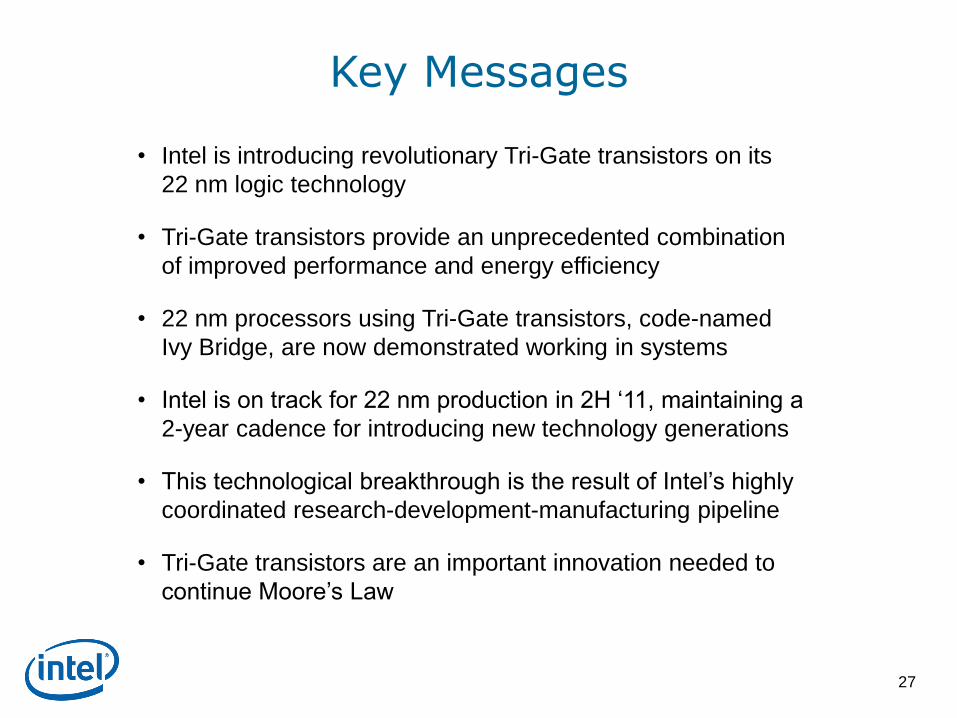
Key Messages
2
• Intel is introducing revolutionary Tri-Gate transistors on its
22 nm logic technology
• Tri-Gate transistors provide an unprecedented combination
of improved performance and energy efficiency
• 22 nm processors using Tri-Gate transistors, code-named
Ivy Bridge, are now demonstrated working in systems
• Intel is on track for 22 nm production in 2H „11, maintaining a
2-year cadence for introducing new technology generations
• This technological breakthrough is the result of Intel‟s highly
coordinated research-development-manufacturing pipeline
• Tri-Gate transistors are an important innovation needed to
continue Moore‟s Law

Intel Technology Roadmap
3
Process Name P1266 P1268 P1270 P1272 P1274
Lithography 45 nm 32 nm 22 nm 14 nm 10 nm
1st Production 2007 2009 2011 2013 2015
Intel continues our cadence of introducing a
new technology generation every two years
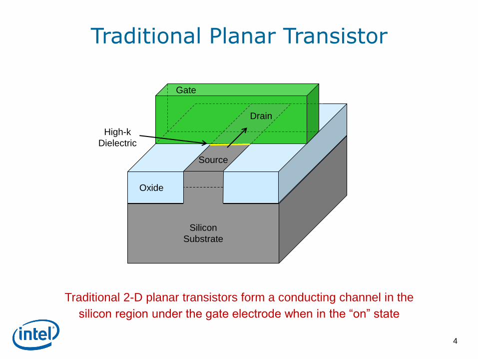
Traditional Planar Transistor
Traditional 2-D planar transistors form a conducting channel in the
silicon region under the gate electrode when in the “on” state
Silicon
Substrate
Oxide
Gate
Source
Drain
High-k
Dielectric
4
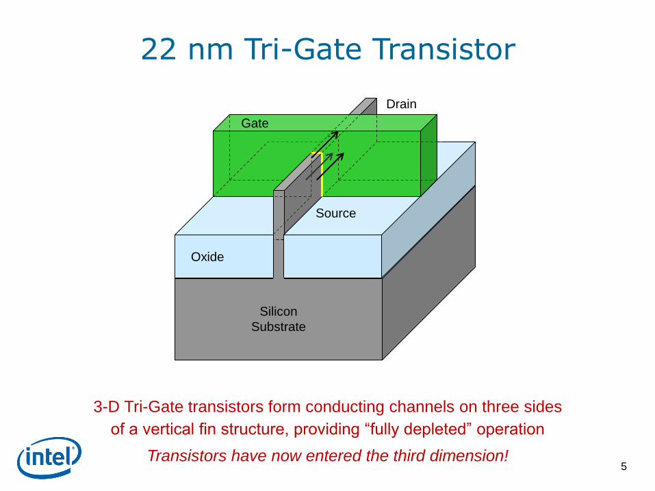
22 nm Tri-Gate Transistor
Silicon
Substrate
Oxide
Source
Drain
Gate
5
3-D Tri-Gate transistors form conducting channels on three sides
of a vertical fin structure, providing “fully depleted” operation
Transistors have now entered the third dimension!
Silicon
Substrate
Oxide
Gate
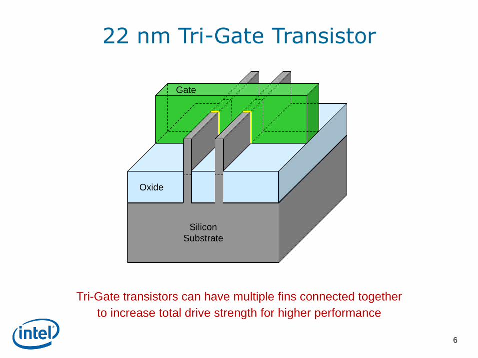
22 nm Tri-Gate Transistor
6
Tri-Gate transistors can have multiple fins connected together
to increase total drive strength for higher performance
Silicon
Substrate
Oxide
Gate
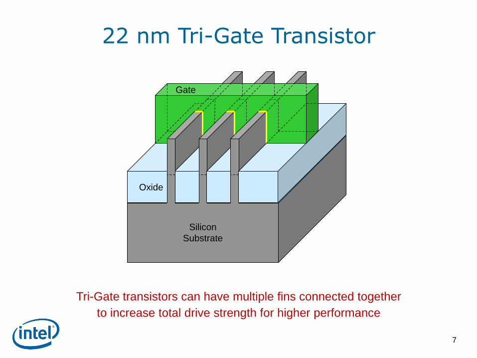
22 nm Tri-Gate Transistor
7
Tri-Gate transistors can have multiple fins connected together
to increase total drive strength for higher performance

22 nm Tri-Gate Transistor
Gates
8
Fins
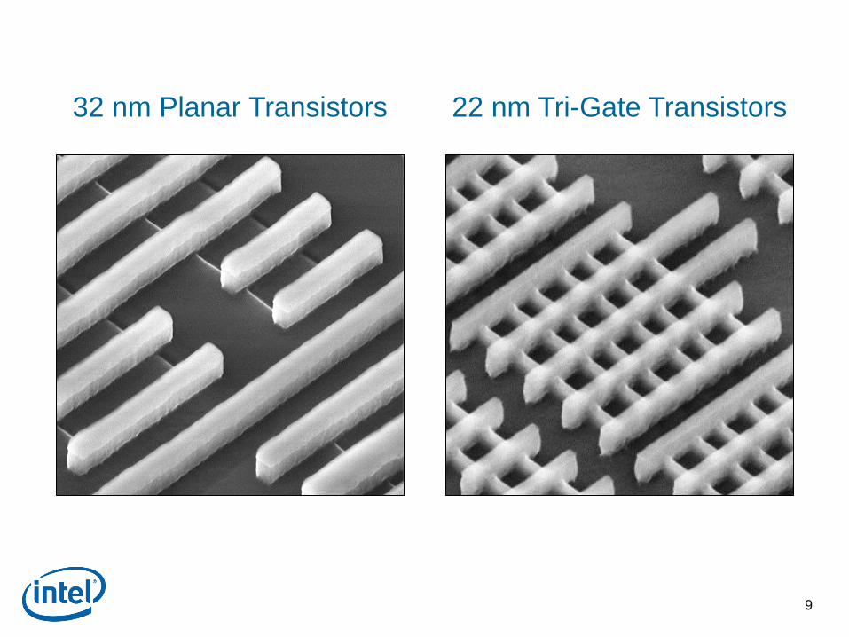
32 nm Planar Transistors
9
22 nm Tri-Gate Transistors

Intel Transistor Leadership
10
2003 2005 2007 2009 2011
90 nm 65 nm 45 nm 32 nm 22 nm
SiGeSiGe
Invented
SiGe
Strained Silicon
2nd Gen.
SiGe
Strained Silicon
2nd Gen.
Gate-Last
High-k
Metal Gate
Invented
Gate-Last
High-k
Metal Gate
First to
Implement
Tri-Gate
Strained Silicon High-k Metal Gate
Tri-Gate
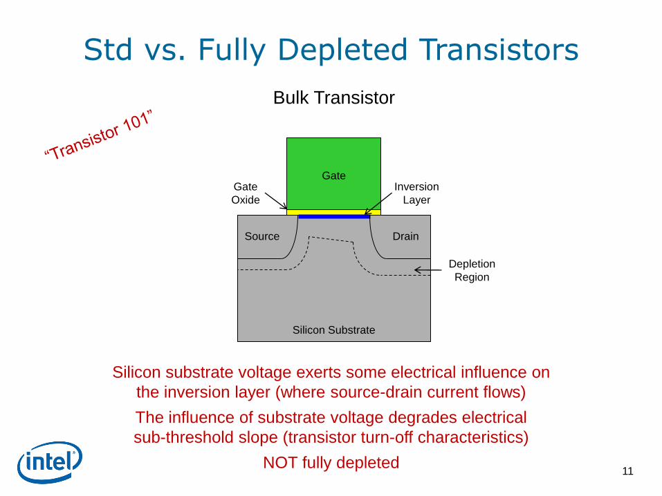
Std vs. Fully Depleted Transistors
Gate
Silicon Substrate
Source
Gate
Oxide
Inversion
Layer
Depletion
Region
Drain
Silicon substrate voltage exerts some electrical influence on
the inversion layer (where source-drain current flows)
The influence of substrate voltage degrades electrical
sub-threshold slope (transistor turn-off characteristics)
NOT fully depleted
Bulk Transistor
11
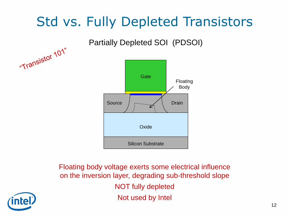
Std vs. Fully Depleted Transistors
Gate
Silicon Substrate
Source
Floating
Body
Drain
Oxide
Partially Depleted SOI (PDSOI)
Floating body voltage exerts some electrical influence
on the inversion layer, degrading sub-threshold slope
NOT fully depleted
Not used by Intel 12

Std vs. Fully Depleted Transistors
Gate
Silicon Substrate
Source Drain
Oxide
Fully Depleted SOI (FDSOI)
Floating body eliminated and sub-threshold slope improved
Requires expensive extremely-thin SOI wafer,
which adds ~10% to total process cost
Not used by Intel 13
Extremely thin
silicon layer
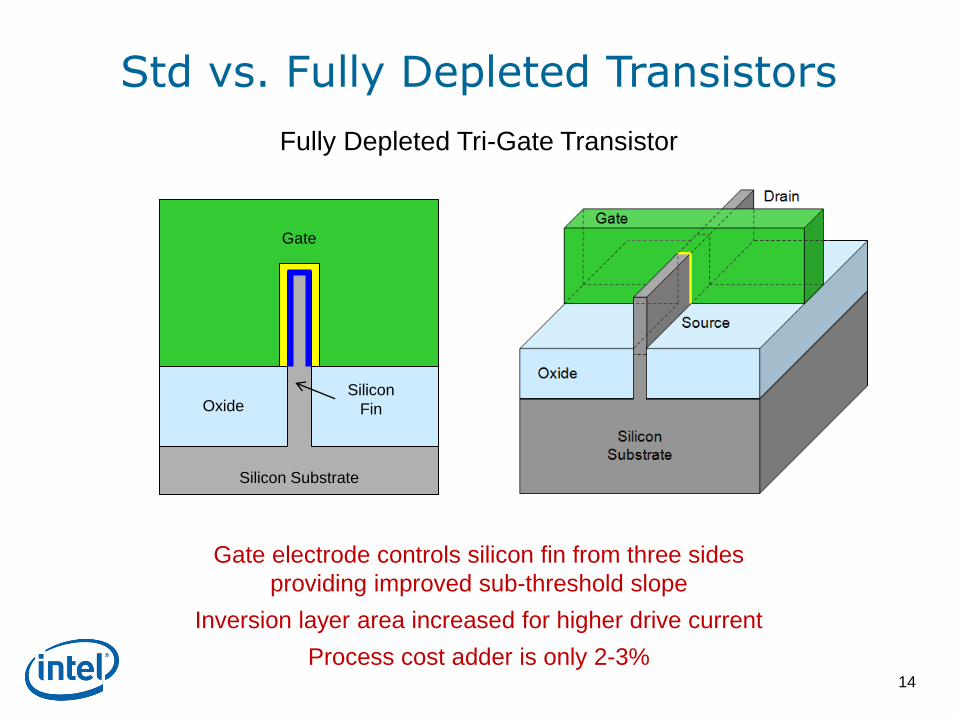
Std vs. Fully Depleted Transistors
Fully Depleted Tri-Gate Transistor
Gate electrode controls silicon fin from three sides
providing improved sub-threshold slope
Inversion layer area increased for higher drive current
Process cost adder is only 2-3%
Gate
Silicon Substrate
Oxide Silicon
Fin
14

Transistor Operation
Gate Voltage (V)
“On”
Current
“Off”
Current
Threshold
Voltage
Operating
Voltage
Channel
Current (normalized)
15
Transistor current-voltage characteristics
Planar

Planar
Tri-Gate
Reduced
Leakage
Gate Voltage (V)
Channel
Current (normalized)
Transistor Operation
16
The “fully depleted” characteristics of Tri-Gate transistors provide a
steeper sub-threshold slope that reduces leakage current

Channel
Current (normalized)
Tri-Gate
Tri-Gate Reduced Threshold
Voltage
Reduced Operating
Voltage Gate Voltage (V)
Transistor Operation
17
The steeper sub-threshold slope can also be used to target a
lower threshold voltage, allowing the transistors to operate at
lower voltage to reduce power and/or improve switching speed

Transistor Gate Delay
Operating Voltage (V)
32 nm
Planar
Lower Voltage
Slower Transistor
Gate Delay
(normalized)
18
Transistor gate delay (switching speed) slows down
as operating voltage is reduced
32 nm
Planar
22 nm
Planar
Operating Voltage (V)
Transistor
Gate Delay
(normalized)
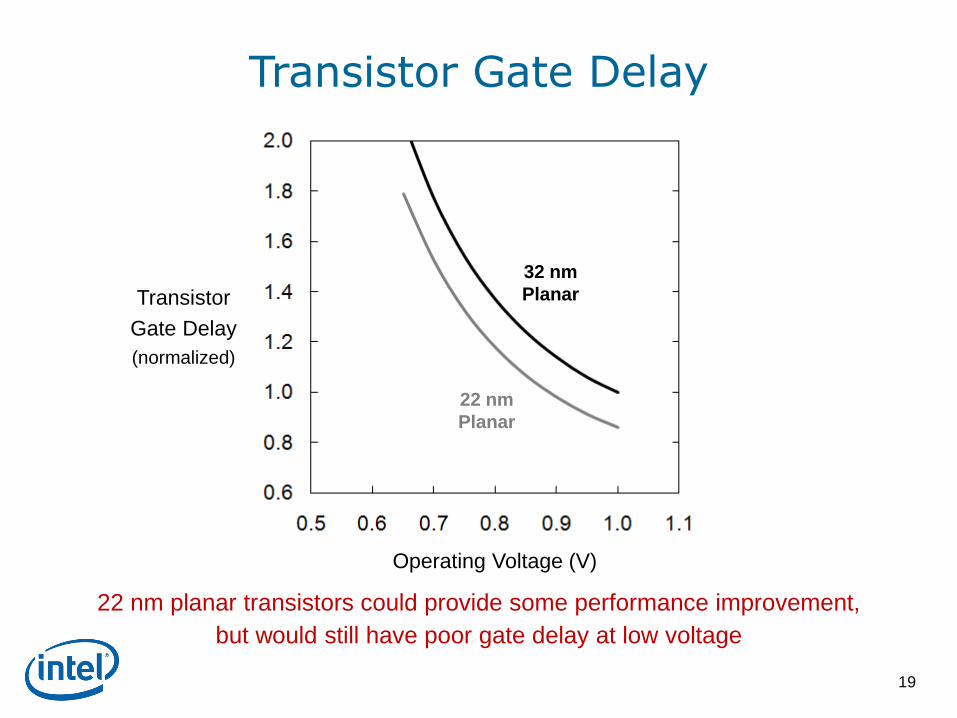
Transistor Gate Delay
19
22 nm planar transistors could provide some performance improvement,
but would still have poor gate delay at low voltage
22 nm
Tri-Gate
32 nm
Planar
18% Faster
37% Faster
Operating Voltage (V)
Transistor
Gate Delay
(normalized)
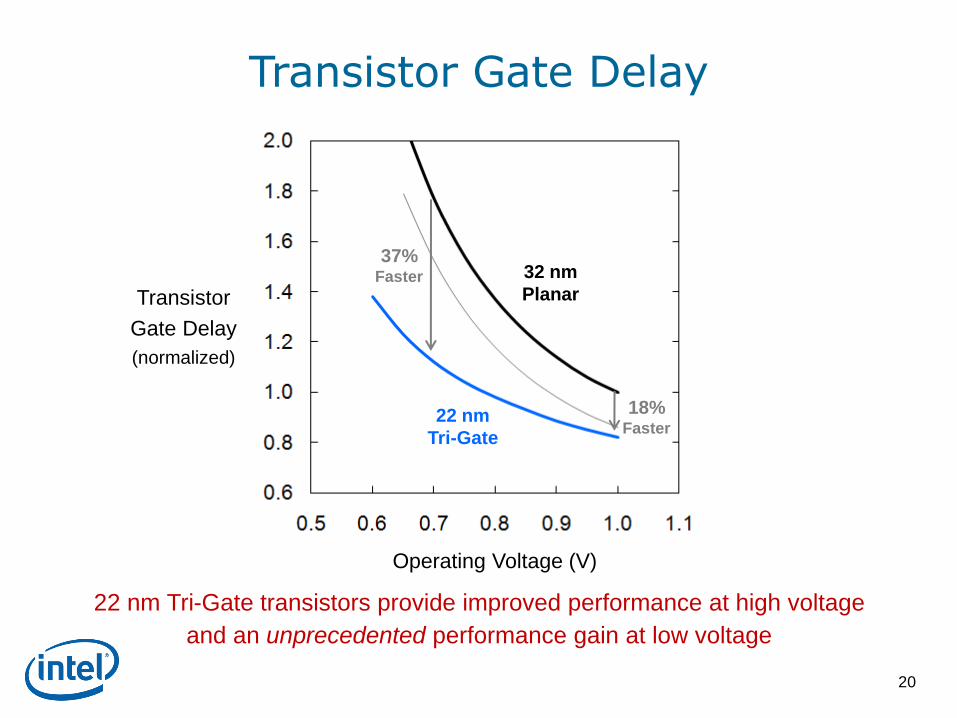
Transistor Gate Delay
20
22 nm Tri-Gate transistors provide improved performance at high voltage
and an unprecedented performance gain at low voltage
22 nm
Tri-Gate
32 nm
Planar
-0.2 V
Operating Voltage (V)
Transistor
Gate Delay
(normalized)
Transistor Gate Delay
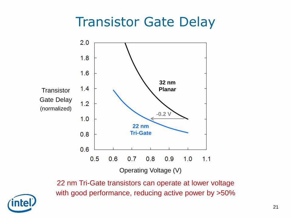
21
22 nm Tri-Gate transistors can operate at lower voltage
with good performance, reducing active power by >50%

Tri-Gate Transistor Benefits
Tri-Gate transistors are an important innovation needed to continue Moore‟s Law
22
• Dramatic performance gain at low operating
voltage, better than Bulk, PDSOI or FDSOI
37% performance increase at low voltage
>50% power reduction at constant performance
• Improved switching characteristics
(On current vs. Off current)
• Higher drive current for a given transistor
footprint
• Only 2-3% cost adder (vs. ~10% for FDSOI)
22 nm Tri-Gate Circuits
23
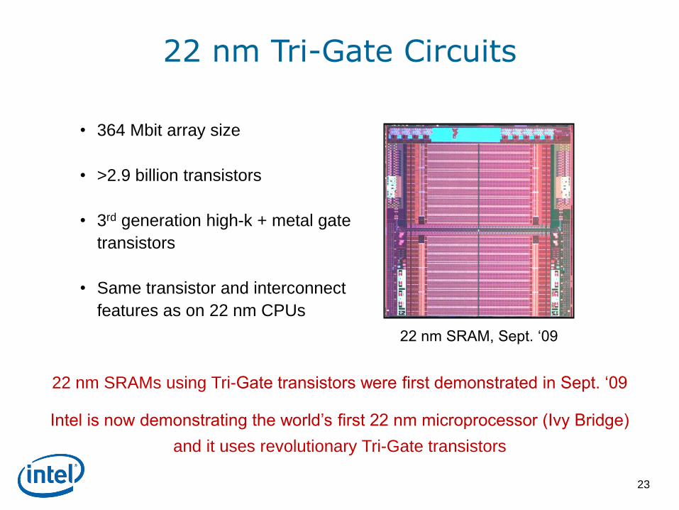
• 364 Mbit array size
• >2.9 billion transistors
• 3rd generation high-k + metal gate
transistors
• Same transistor and interconnect
features as on 22 nm CPUs
22 nm SRAM, Sept. „09
22 nm SRAMs using Tri-Gate transistors were first demonstrated in Sept. „09
Intel is now demonstrating the world‟s first 22 nm microprocessor (Ivy Bridge)
and it uses revolutionary Tri-Gate transistors
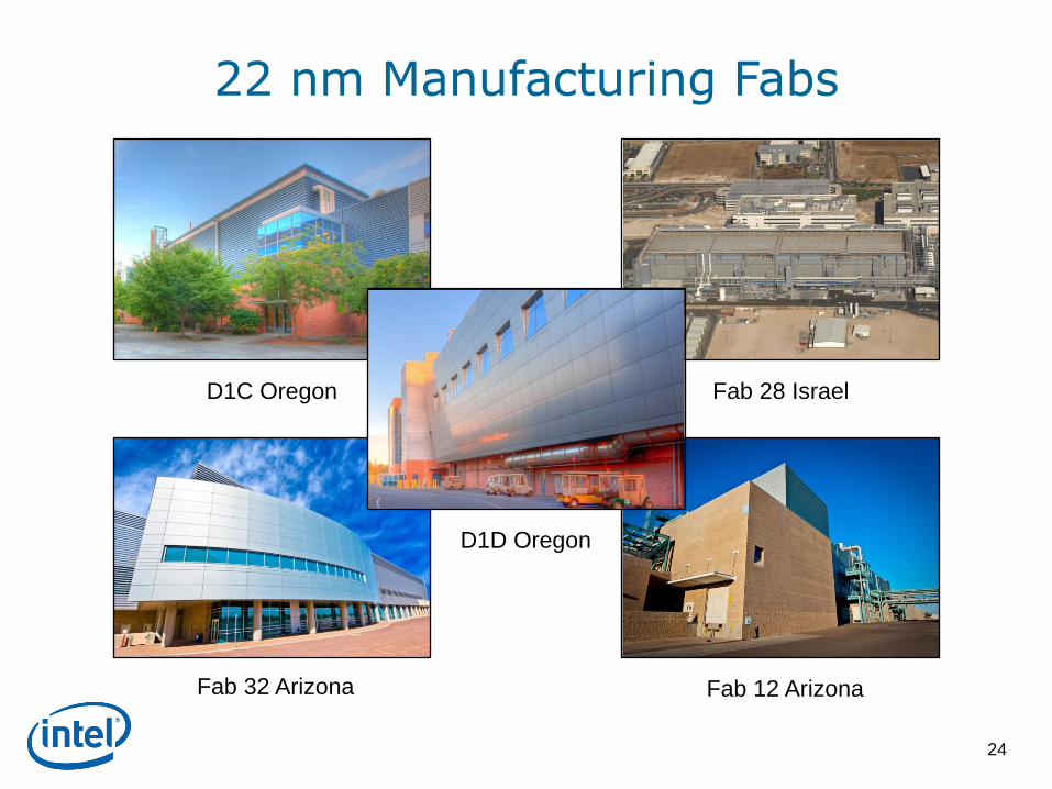
22 nm Manufacturing Fabs
D1C Oregon
Fab 12 Arizona
D1D Oregon
Fab 32 Arizona
Fab 28 Israel
24

Intel continues to successfully introduce leading edge
process + products on a 2 year cadence
On-Time 2 Year Cycles
25
90 nm
2003
45 nm
2007
65 nm
2005
32 nm
2009
22 nm
2011
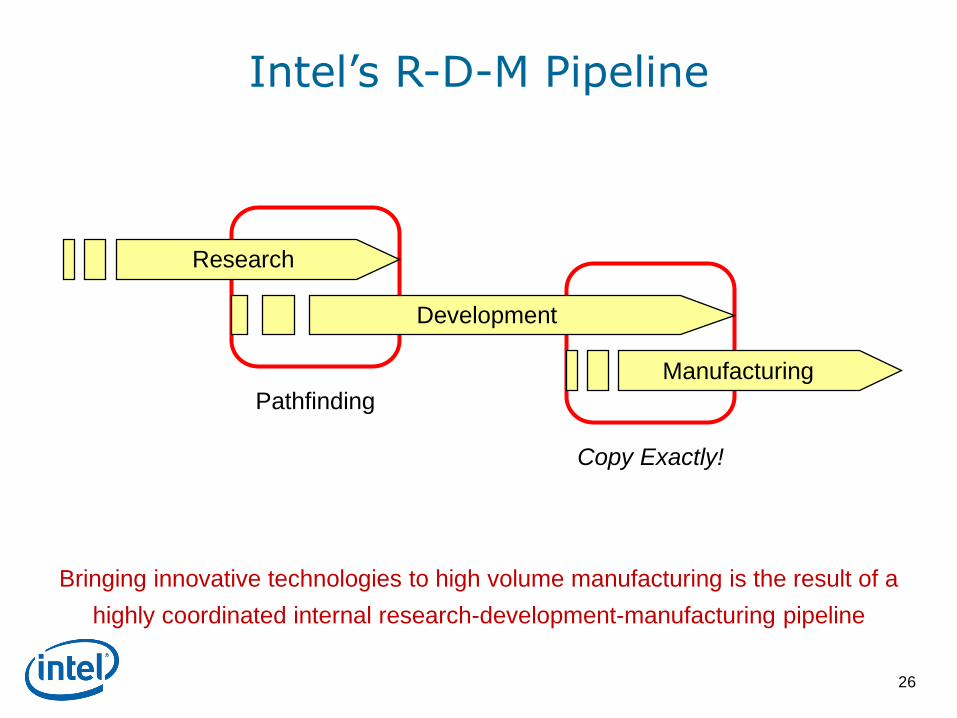
Intel’s R-D-M Pipeline
26
Pathfinding
Copy Exactly!
Development
Manufacturing
Research
Bringing innovative technologies to high volume manufacturing is the result of a
highly coordinated internal research-development-manufacturing pipeline
Key Messages
27
• Intel is introducing revolutionary Tri-Gate transistors on its
22 nm logic technology
• Tri-Gate transistors provide an unprecedented combination
of improved performance and energy efficiency
• 22 nm processors using Tri-Gate transistors, code-named
Ivy Bridge, are now demonstrated working in systems
• Intel is on track for 22 nm production in 2H „11, maintaining a
2-year cadence for introducing new technology generations
• This technological breakthrough is the result of Intel‟s highly
coordinated research-development-manufacturing pipeline
• Tri-Gate transistors are an important innovation needed to
continue Moore‟s Law
