intel386tm sx microprocessor - digi-key sheets/intel pdfs/intel386 sx.pdf · intel386 sx...
TRANSCRIPT

*Other brands and names are the property of their respective owners.Information in this document is provided in connection with Intel products. Intel assumes no liability whatsoever, including infringement of any patent orcopyright, for sale and use of Intel products except as provided in Intel’s Terms and Conditions of Sale for such products. Intel retains the right to makechanges to these specifications at any time, without notice. Microcomputer Products may have minor variations to this specification known as errata.
January 1994COPYRIGHT © INTEL CORPORATION, 1995 Order Number: 240187-008
Intel386TM SX MICROPROCESSOR
Y Full 32-Bit Internal ArchitectureÐ 8-, 16-, 32-Bit Data TypesÐ 8 General Purpose 32-Bit Registers
Y Runs Intel386TM Software in a CostEffective 16-Bit Hardware EnvironmentÐ Runs Same Applications and O.S.’s
as the Intel386TM DX ProcessorÐ Object Code Compatible with 8086,
80186, 80286, and Intel386TM
Processors
Y High Performance 16-Bit Data BusÐ 16, 20, 25 and 33 MHz ClockÐ Two-Clock Bus CyclesÐ Address Pipelining Allows Use of
Slower/Cheaper Memories
Y Integrated Memory Management UnitÐ Virtual Memory SupportÐ Optional On-Chip PagingÐ 4 Levels of Hardware Enforced
ProtectionÐ MMU Fully Compatible with Those of
the 80286 and Intel386 DX CPUs
Y Virtual 8086 Mode Allows Execution of8086 Software in a Protected andPaged System
Y Large Uniform Address SpaceÐ 16 Megabyte PhysicalÐ 64 Terabyte VirtualÐ 4 Gigabyte Maximum Segment Size
Y Numerics Support with the Intel387TM
SX Math CoProcessor
Y On-Chip Debugging Support IncludingBreakpoint Registers
Y Complete System DevelopmentSupportÐ Software: C, PL/M, AssemblerÐ Debuggers: PMON-386 DX,
ICETM-386 SX
Y High Speed CHMOS IV Technology
Y Operating Frequency:Ð Standard
(Intel386 SX -33, -25, -20, -16)Min/Max Frequency(4/33, 4/25, 4/20, 4/16) MHz
Ð Low Power(Intel386 SX -33, -25, -20, -16, -12)Min/Max Frequency(2/33, 2/25, 2/20, 2/16, 2/12) MHz
Y 100-Pin Plastic Quad Flatpack Package(See Packaging Outlines and Dimensions Ý231369)
The Intel386TM SX Microprocessor is an entry-level 32-bit CPU with a 16-bit external data bus and a 24-bitexternal address bus. The Intel386 SX CPU brings the vast software library of the Intel386TM Architecture toentry-level systems. It provides the performance benefits of a 32-bit programming architecture with the costsavings associated with 16-bit hardware systems.
240187–47
Intel386TM SX Pipelined 32-Bit Microarchitecture

Intel386TM SX MICROPROCESSOR
Intel386TM SX MicroProcessor
CONTENTS PAGE
1.0 PIN DESCRIPTION ÀÀÀÀÀÀÀÀÀÀÀÀÀÀÀÀÀÀÀÀ 3
2.0 BASE ARCHITECTURE ÀÀÀÀÀÀÀÀÀÀÀÀÀÀÀÀ 6
2.1 Register Set ÀÀÀÀÀÀÀÀÀÀÀÀÀÀÀÀÀÀÀÀÀÀÀÀÀÀÀÀ 6
2.2 Instruction Set ÀÀÀÀÀÀÀÀÀÀÀÀÀÀÀÀÀÀÀÀÀÀÀÀÀ 10
2.3 Memory Organization ÀÀÀÀÀÀÀÀÀÀÀÀÀÀÀÀÀÀ 11
2.4 Addressing Modes ÀÀÀÀÀÀÀÀÀÀÀÀÀÀÀÀÀÀÀÀ 12
2.5 Data Types ÀÀÀÀÀÀÀÀÀÀÀÀÀÀÀÀÀÀÀÀÀÀÀÀÀÀÀÀ 15
2.6 I/O Space ÀÀÀÀÀÀÀÀÀÀÀÀÀÀÀÀÀÀÀÀÀÀÀÀÀÀÀÀÀ 15
2.7 Interrupts and Exceptions ÀÀÀÀÀÀÀÀÀÀÀÀÀÀ 17
2.8 Reset and Initialization ÀÀÀÀÀÀÀÀÀÀÀÀÀÀÀÀÀ 20
2.9 Testability ÀÀÀÀÀÀÀÀÀÀÀÀÀÀÀÀÀÀÀÀÀÀÀÀÀÀÀÀÀ 20
2.10 Debugging Support ÀÀÀÀÀÀÀÀÀÀÀÀÀÀÀÀÀÀÀ 21
3.0 REAL MODE ARCHITECTURE ÀÀÀÀÀÀÀ 22
3.1 Memory Addressing ÀÀÀÀÀÀÀÀÀÀÀÀÀÀÀÀÀÀÀ 22
3.2 Reserved Locations ÀÀÀÀÀÀÀÀÀÀÀÀÀÀÀÀÀÀÀ 23
3.3 Interrupts ÀÀÀÀÀÀÀÀÀÀÀÀÀÀÀÀÀÀÀÀÀÀÀÀÀÀÀÀÀÀ 23
3.4 Shutdown and Halt ÀÀÀÀÀÀÀÀÀÀÀÀÀÀÀÀÀÀÀÀ 23
3.5 LOCK Operations ÀÀÀÀÀÀÀÀÀÀÀÀÀÀÀÀÀÀÀÀÀ 23
4.0 PROTECTED MODEARCHITECTURE ÀÀÀÀÀÀÀÀÀÀÀÀÀÀÀÀÀÀÀÀÀÀÀ 24
4.1 Addressing Mechanism ÀÀÀÀÀÀÀÀÀÀÀÀÀÀÀÀ 24
4.2 Segmentation ÀÀÀÀÀÀÀÀÀÀÀÀÀÀÀÀÀÀÀÀÀÀÀÀÀ 24
4.3 Protection ÀÀÀÀÀÀÀÀÀÀÀÀÀÀÀÀÀÀÀÀÀÀÀÀÀÀÀÀÀ 29
4.4 Paging ÀÀÀÀÀÀÀÀÀÀÀÀÀÀÀÀÀÀÀÀÀÀÀÀÀÀÀÀÀÀÀÀ 33
4.5 Virtual 8086 Environment ÀÀÀÀÀÀÀÀÀÀÀÀÀÀ 36
CONTENTS PAGE
5.0 FUNCTIONAL DATA ÀÀÀÀÀÀÀÀÀÀÀÀÀÀÀÀÀ 39
5.1 Signal Description Overview ÀÀÀÀÀÀÀÀÀÀÀ 39
5.2 Bus Transfer Mechanism ÀÀÀÀÀÀÀÀÀÀÀÀÀÀ 45
5.3 Memory and I/O Spaces ÀÀÀÀÀÀÀÀÀÀÀÀÀÀ 45
5.4 Bus Functional Description ÀÀÀÀÀÀÀÀÀÀÀÀ 45
5.5 Self-test Signature ÀÀÀÀÀÀÀÀÀÀÀÀÀÀÀÀÀÀÀÀÀ 63
5.6 Component and RevisionIdentifiers ÀÀÀÀÀÀÀÀÀÀÀÀÀÀÀÀÀÀÀÀÀÀÀÀÀÀÀÀÀÀÀ 63
5.7 Coprocessor Interfacing ÀÀÀÀÀÀÀÀÀÀÀÀÀÀÀ 63
6.0 PACKAGE THERMALSPECIFICATIONS ÀÀÀÀÀÀÀÀÀÀÀÀÀÀÀÀÀÀÀÀÀÀ 64
7.0 ELECTRICAL SPECIFICATIONS ÀÀÀÀÀ 64
7.1 Power and Grounding ÀÀÀÀÀÀÀÀÀÀÀÀÀÀÀÀÀ 64
7.2 Maximum Ratings ÀÀÀÀÀÀÀÀÀÀÀÀÀÀÀÀÀÀÀÀÀ 65
7.3 D.C. Specifications ÀÀÀÀÀÀÀÀÀÀÀÀÀÀÀÀÀÀÀÀ 66
7.4 A.C. Specifications ÀÀÀÀÀÀÀÀÀÀÀÀÀÀÀÀÀÀÀÀ 68
7.5 Designing for ICETM-Intel386 SXEmulator ÀÀÀÀÀÀÀÀÀÀÀÀÀÀÀÀÀÀÀÀÀÀÀÀÀÀÀÀÀÀÀÀ 78
8.0 DIFFERENCES BETWEEN THEIntel386TM SX CPU and theIntel386TM DX CPU ÀÀÀÀÀÀÀÀÀÀÀÀÀÀÀÀÀÀÀÀ 79
9.0 INSTRUCTION SET ÀÀÀÀÀÀÀÀÀÀÀÀÀÀÀÀÀÀÀ 80
9.1 Intel386TM SX CPU InstructionEncoding and Clock Count Summary ÀÀÀÀ 80
9.2 Instruction Encoding ÀÀÀÀÀÀÀÀÀÀÀÀÀÀÀÀÀÀÀ 95
2

Intel386TM SX MICROPROCESSOR
1.0 PIN DESCRIPTION
240187–1
NOTE:NC e No Connect
Figure 1.1. Intel386TM SX Microprocessor Pin out Top View
Table 1.1. Alphabetical Pin Assignments
Address Data Control N/C VCC VSS
A1 18 D0 1 ADSÝ 16 20 8 2A2 51 D1 100 BHEÝ 19 27 9 5A3 52 D2 99 BLEÝ 17 29 10 11A4 53 D3 96 BUSYÝ 34 30 21 12A5 54 D4 95 CLK2 15 31 32 13A6 55 D5 94 D/CÝ 24 43 39 14A7 56 D6 93 ERRORÝ 36 44 42 22A8 58 D7 92 FLTÝ 28 45 48 35A9 59 D8 90 HLDA 3 46 57 41A10 60 D9 89 HOLD 4 47 69 49A11 61 D10 88 INTR 40 71 50A12 62 D11 87 LOCKÝ 26 84 63A13 64 D12 86 M/IOÝ 23 91 67A14 65 D13 83 NAÝ 6 97 68A15 66 D14 82 NMI 38 77A16 70 D15 81 PEREQ 37 78A17 72 READYÝ 7 85A18 73 RESET 33 98A19 74 W/RÝ 25A20 75A21 76A22 79A23 80
3

Intel386TM SX MICROPROCESSOR
1.0 PIN DESCRIPTION (Continued)
The following are the Intel386TM SX Microprocessor pin descriptions. The following definitions are used in thepin descriptions:
Ý The named signal is active LOW.I Input signal.O Output signal.I/O Input and Output signal.- No electrical connection.
Symbol Type Pin Name and Function
CLK2 I 15 CLK2 provides the fundamental timing for the Intel386 SXMicroprocessor. For additional information see Clock.
RESET I 33 RESET suspends any operation in progress and places theIntel386 SX Microprocessor in a known reset state. SeeInterrupt Signals for additional information.
D15–D0 I/O 81-83,86-90, Data Bus inputs data during memory, I/O and interruptacknowledge read cycles and outputs data during memory and92-96,99-100,1I/O write cycles. See Data Bus for additional information.
A23–A1 O 80-79,76-72,70, Address Bus outputs physical memory or port I/O addresses.See Address Bus for additional information.66-64,62-58,
56-51,18
W/RÝ O 25 Write/Read is a bus cycle definition pin that distinguishes writecycles from read cycles. See Bus Cycle Definition Signals foradditional information.
D/CÝ O 24 Data/Control is a bus cycle definition pin that distinguishes datacycles, either memory or I/O, from control cycles which are:interrupt acknowledge, halt, and code fetch. See Bus CycleDefinition Signals for additional information.
M/IOÝ O 23 Memory/IO is a bus cycle definition pin that distinguishesmemory cycles from input/output cycles. See Bus CycleDefinition Signals for additional information.
LOCKÝ O 26 Bus Lock is a bus cycle definition pin that indicates that othersystem bus masters are not to gain control of the system buswhile it is active. See Bus Cycle Definition Signals foradditional information.
ADSÝ O 16 Address Status indicates that a valid bus cycle definition andaddress (W/RÝ, D/CÝ, M/IOÝ, BHEÝ, BLEÝ and A23–A1 arebeing driven at the Intel386 SX Microprocessor pins. See BusControl Signals for additional information.
NAÝ I 6 Next Address is used to request address pipelining. See BusControl Signals for additional information.
READYÝ I 7 Bus Ready terminates the bus cycle. See Bus Control Signalsfor additional information.
BHEÝ, BLEÝ O 19,17 Byte Enables indicate which data bytes of the data bus take partin a bus cycle. See Address Bus for additional information.
4

Intel386TM SX MICROPROCESSOR
1.0 PIN DESCRIPTION (Continued)
Symbol Type Pin Name and Function
HOLD I 4 Bus Hold Request input allows another bus master to requestcontrol of the local bus. See Bus Arbitration Signals foradditional information.
HLDA O 3 Bus Hold Acknowledge output indicates that the Intel386 SXMicroprocessor has surrendered control of its local bus toanother bus master. See Bus Arbitration Signals for additionalinformation.
INTR I 40 Interrupt Request is a maskable input that signals the Intel386SX Microprocessor to suspend execution of the current programand execute an interrupt acknowledge function. See InterruptSignals for additional information.
NMI I 38 Non-Maskable Interrupt Request is a non-maskable input thatsignals the Intel386 SX Microprocessor to suspend execution ofthe current program and execute an interrupt acknowledgefunction. See Interrupt Signals for additional information.
BUSYÝ I 34 Busy signals a busy condition from a processor extension. SeeCoprocessor Interface Signals for additional information.
ERRORÝ I 36 Error signals an error condition from a processor extension. SeeCoprocessor Interface Signals for additional information.
PEREQ I 37 Processor Extension Request indicates that the processor hasdata to be transferred by the Intel386 SX Microprocessor. SeeCoprocessor Interface Signals for additional information.
FLTÝ I 28 Float is an input which forces all bidirectional and output signals,including HLDA, to the tri-state condition. This allows theelectrically isolated Intel386SX PQFP to use ONCE (On-CircuitEmulation) method without removing it from the PCB. See Floatfor additional information.
N/C - 20, 27, 29-31, 43-47 No Connects should always be left unconnected. Connection ofa N/C pin may cause the processor to malfunction or beincompatible with future steppings of the Intel386 SXMicroprocessor.
VCC I 8-10,21,32,39 System Power provides the a5V nominal DC supply input.
42,48,57,69,
71,84,91,97
VSS I 2,5,11-14,22 System Ground provides the 0V connection from which allinputs and outputs are measured.35,41,49-50,
63,67-68,
77-78,85,98
5

Intel386TM SX MICROPROCESSOR
INTRODUCTION
The Intel386 SX Microprocessor is 100% objectcode compatible with the Intel386 DX, 286 and 8086microprocessors. Systems based on the Intel386 SXCPU can access the world’s largest existing micro-computer software base, including the growing 32-bit software base.
Instruction pipelining and a high performance ALUensure short average instruction execution timesand high system throughput.
The integrated memory management unit (MMU) in-cludes an address translation cache, multi-taskinghardware, and a four-level hardware-enforced pro-tection mechanism to support operating systems.The virtual machine capability of the Intel386 SXCPU allows simultaneous execution of applicationsfrom multiple operating systems.
The Intel386 SX CPU offers on-chip testability anddebugging features. Four breakpoint registers allowconditional or unconditional breakpoint traps oncode execution or data accesses for powerful de-bugging of even ROM-based systems. Other testa-bility features include self-test, tri-state of outputbuffers, and direct access to the page translationcache.
The Low Power Intel386 SX CPU brings the benefitsof the Intel386 Microprocessor 32-bit architecture toLaptop and Notebook personal computer applica-tions. With its power saving 2 MHz sleep-mode andextended functional temperature range of 0§C to100§C TCASE, the Lower Power Intel386 SX CPUspecifically satisfies the power consumption andheat dissipation requirements of today’s small formfactor computers.
2.0 BASE ARCHITECTURE
The Intel386 SX Microprocessor consists of a cen-tral processing unit, a memory management unit anda bus interface.
The central processing unit consists of the execu-tion unit and the instruction unit. The execution unitcontains the eight 32-bit general purpose registerswhich are used for both address calculation anddata operations and a 64-bit barrel shifter used tospeed shift, rotate, multiply, and divide operations.The instruction unit decodes the instruction opcodes
and stores them in the decoded instruction queuefor immediate use by the execution unit.
The memory management unit (MMU) consists of asegmentation unit and a paging unit. Segmentationallows the managing of the logical address space byproviding an extra addressing component, one thatallows easy code and data relocatability, and effi-cient sharing. The paging mechanism operates be-neath and is transparent to the segmentation pro-cess, to allow management of the physical addressspace.
The segmentation unit provides four levels of pro-tection for isolating and protecting applications andthe operating system from each other. The hardwareenforced protection allows the design of systemswith a high degree of integrity.
The Intel386 SX Microprocessor has two modes ofoperation: Real Address Mode (Real Mode), andProtected Virtual Address Mode (Protected Mode).In Real Mode the Intel386 SX Microprocessor oper-ates as a very fast 8086, but with 32-bit extensions ifdesired. Real Mode is required primarily to set up theprocessor for Protected Mode operation.
Within Protected Mode, software can perform a taskswitch to enter into tasks designated as Virtual 8086Mode tasks. Each such task behaves with 8086 se-mantics, thus allowing 8086 software (an applicationprogram or an entire operating system) to execute.The Virtual 8086 tasks can be isolated and protect-ed from one another and the host Intel386 SX Micro-processor operating system by use of paging.
Finally, to facilitate system hardware designs, theIntel386 SX Microprocessor bus interface offers ad-dress pipelining and direct Byte Enable signals foreach byte of the data bus.
2.1 Register Set
The Intel386 SX Microprocessor has thirty-four reg-isters as shown in Figure 2-1. These registers aregrouped into the following seven categories:
General Purpose Registers: The eight 32-bit gen-eral purpose registers are used to contain arithmeticand logical operands. Four of these (EAX, EBX,ECX, and EDX) can be used either in their entirety as32-bit registers, as 16-bit registers, or split into pairsof separate 8-bit registers.
6

Intel386TM SX MICROPROCESSOR
240187–2
Figure 2.1. Intel386TM SX Microprocessor Registers
7

Intel386TM SX MICROPROCESSOR
Segment Registers: Six 16-bit special purpose reg-isters select, at any given time, the segments ofmemory that are immediately addressable for code,stack, and data.
Flags and Instruction Pointer Registers: The two32-bit special purpose registers in figure 2.1 recordor control certain aspects of the Intel386 SX Micro-processor state. The EFLAGS register includesstatus and control bits that are used to reflect theoutcome of many instructions and modify the se-mantics of some instructions. The Instruction Point-er, called EIP, is 32 bits wide. The Instruction Pointercontrols instruction fetching and the processor auto-matically increments it after executing an instruction.
Control Registers: The four 32-bit control registerare used to control the global nature of the Intel386SX Microprocessor. The CR0 register contains bitsthat set the different processor modes (Protected,Real, Paging and Coprocessor Emulation). CR2 andCR3 registers are used in the paging operation.
System Address Registers: These four specialregisters reference the tables or segments support-ed by the 80286/Intel386 SX/Intel386 DX CPU’sprotection model. These tables or segments are:
GDTR (Global Descriptor Table Register),IDTR (Interrupt Descriptor Table Register),LDTR (Local Descriptor Table Register),TR (Task State Segment Register).
Debug Registers: The six programmer accessibledebug registers provide on-chip support for debug-ging. The use of the debug registers is described inSection 2.10 Debugging Support.
Test Registers: Two registers are used to controlthe testing of the RAM/CAM (Content AddressableMemories) in the Translation Lookaside Buffer por-tion of the Intel386 SX Microprocessor. Their use isdiscussed in Testability.
240187–3
Figure 2.2. Status and Control Register Bit Functions
8

Intel386TM SX MICROPROCESSOR
EFLAGS REGISTER
The flag register is a 32-bit register named EFLAGS.The defined bits and bit fields within EFLAGS,shown in Figure 2.2, control certain operations andindicate the status of the Intel386 SX Microproces-sor. The lower 16 bits (bits 0–15) of EFLAGS con-tain the 16-bit flag register named FLAGS. This isthe default flag register used when executing 8086,80286, or real mode code. The functions of the flagbits are given in Table 2.1.
CONTROL REGISTERS
The Intel386 SX Microprocessor has three controlregisters of 32 bits, CR0, CR2 and CR3, to hold themachine state of a global nature. These registersare shown in Figures 2.1 and 2.2. The defined CR0bits are described in Table 2.2.
Table 2.1. Flag Definitions
Bit Position Name Function
0 CF Carry FlagÐSet on high-order bit carry or borrow; clearedotherwise.
2 PF Parity FlagÐSet if low-order 8 bits of result contain an evennumber of 1-bits; cleared otherwise.
4 AF Auxiliary Carry FlagÐSet on carry from or borrow to the loworder four bits of AL; cleared otherwise.
6 ZF Zero FlagÐSet if result is zero; cleared otherwise.
7 SF Sign FlagÐSet equal to high-order bit of result (0 if positive, 1 ifnegative).
8 TF Single Step FlagÐOnce set, a single step interrupt occurs afterthe next instruction executes. TF is cleared by the single stepinterrupt.
9 IF Interrupt-Enable FlagÐWhen set, maskable interrupts will causethe CPU to transfer control to an interrupt vector specifiedlocation.
10 DF Direction FlagÐCauses string instructions to auto-increment(default) the appropriate index registers when cleared. SettingDF causes auto-decrement.
11 OF Overflow FlagÐSet if the operation resulted in a carry/borrowinto the sign bit (high-order bit) of the result but did not result in acarry/borrow out of the high-order bit or vice-versa.
12,13 IOPL I/O Privilege LevelÐIndicates the maximum Current PrivilegeLevel (CPL) permitted to execute I/O instructions withoutgenerating an exception 13 fault or consulting the I/O permissionbit map while executing in protected mode. For virtual 86 mode itindicates the maximum CPL allowing alteration of the IF bit. SeeSection 4.2 for a further discussion and definitions on variousprivilege levels.
14 NT Nested TaskÐSet if the execution of the current task is nestedwithin another task. Cleared otherwise.
16 RF Resume FlagÐUsed in conjunction with debug registerbreakpoints. It is checked at instruction boundaries beforebreakpoint processing. If set, any debug fault is ignored on thenext instruction.
17 VM Virtual 8086 ModeÐIf set while in protected mode, the Intel386SX Microprocessor will switch to virtual 8086 operation, handlingsegment loads as the 8086 does, but generating exception 13faults on privileged opcodes.
9

Intel386TM SX MICROPROCESSOR
Table 2.2. CR0 Definitions
Bit Position Name Function
0 PE Protection mode enableÐplaces the Intel386 SX Microprocessorinto protected mode. If PE is reset, the processor operates againin Real Mode. PE may be set by loading MSW or CR0. PE can bereset only by loading CR0, it cannot be reset by the LMSWinstruction.
1 MP Monitor coprocessor extensionÐallows WAIT instructions tocause a processor extension not present exception (number 7).
2 EM Emulate processor extensionÐcauses a processor extensionnot present exception (number 7) on ESC instructions to allowemulating a processor extension.
3 TS Task switchedÐindicates the next instruction using a processorextension will cause exception 7, allowing software to testwhether the current processor extension context belongs to thecurrent task.
31 PG Paging enable bitÐis set to enable the on-chip paging unit. It isreset to disable the on-chip paging unit.
2.2 Instruction Set
The instruction set is divided into nine categories ofoperations:
Data TransferArithmeticShift/RotateString ManipulationBit ManipulationControl TransferHigh Level Language SupportOperating System SupportProcessor Control
These instructions are listed in Table 9.1 Instruc-tion Set Clock Count Summary.
All Intel386 SX Microprocessor instructions operateon either 0, 1, 2 or 3 operands; an operand residesin a register, in the instruction itself, or in memory.Most zero operand instructions (e.g CLI, STI) takeonly one byte. One operand instructions generally
are two bytes long. The average instruction is 3.2bytes long. Since the Intel386 SX Microprocessorhas a 16 byte prefetch instruction queue, an averageof 5 instructions will be prefetched. The use of twooperands permits the following types of common in-structions:
Register to RegisterMemory to RegisterImmediate to RegisterMemory to MemoryRegister to MemoryImmediate to Memory.
The operands can be either 8, 16, or 32 bits long. Asa general rule, when executing code written for theIntel386 SX Microprocessor (32-bit code), operandsare 8 or 32 bits; when executing existing 8086 or80286 code (16-bit code), operands are 8 or 16 bits.Prefixes can be added to all instructions which over-ride the default length of the operands (i.e. use32-bit operands for 16-bit code, or 16-bit operandsfor 32-bit code).
10

Intel386TM SX MICROPROCESSOR
2.3 Memory Organization
Memory on the Intel386 SX Microprocessor is divid-ed into 8-bit quantities (bytes), 16-bit quantities(words), and 32-bit quantities (dwords). Words arestored in two consecutive bytes in memory with thelow-order byte at the lowest address. Dwords arestored in four consecutive bytes in memory with thelow-order byte at the lowest address. The address ofa word or dword is the byte address of the low-orderbyte.
In addition to these basic data types, the Intel386 SXMicroprocessor supports two larger units of memory:pages and segments. Memory can be divided upinto one or more variable length segments, whichcan be swapped to disk or shared between pro-grams. Memory can also be organized into one ormore 4K byte pages. Finally, both segmentation andpaging can be combined, gaining the advantages ofboth systems. The Intel386 SX Microprocessor sup-ports both pages and segmentation in order to pro-vide maximum flexibility to the system designer.Segmentation and paging are complementary. Seg-mentation is useful for organizing memory in logicalmodules, and as such is a tool for the applicationprogrammer, while pages are useful to the systemprogrammer for managing the physical memory of asystem.
ADDRESS SPACES
The Intel386 SX Microprocessor has three types ofaddress spaces: logical, linear, and physical. Alogical address (also known as a virtual address)consists of a selector and an offset. A selector is thecontents of a segment register. An offset is formedby summing all of the addressing components(BASE, INDEX, DISPLACEMENT), discussed in sec-tion 2.4 Addressing Modes, into an effective ad-dress. This effective address along with the selectoris known as the logical address. Since each task onthe Intel386 SX Microprocessor has a maximum of
16K (214 b1) selectors, and offsets can be 4 giga-bytes (with paging enabled) this gives a total of 246
bits, or 64 terabytes, of logical address space pertask. The programmer sees the logical addressspace.
The segmentation unit translates the logical ad-dress space into a 32-bit linear address space. If thepaging unit is not enabled then the 32-bit linear ad-dress is truncated into a 24-bit physical address.The physical address is what appears on the ad-dress pins.
The primary differences between Real Mode andProtected Mode are how the segmentation unit per-forms the translation of the logical address into thelinear address, size of the address space, and pag-ing capability. In Real Mode, the segmentation unitshifts the selector left four bits and adds the result tothe effective address to form the linear address.This linear address is limited to 1 megabyte. In addi-tion, real mode has no paging capability.
Protected Mode will see one of two different ad-dress spaces, depending on whether or not pagingis enabled. Every selector has a logical base ad-dress associated with it that can be up to 32 bits inlength. This 32-bit logical base address is added tothe effective address to form a final 32-bit linearaddress. If paging is disabled this final linear ad-dress reflects physical memory and is truncated sothat only the lower 24 bits of this address are usedto address the 16 megabyte memory address space.If paging is enabled this final linear address reflectsa 32-bit address that is translated through the pag-ing unit to form a 16-megabyte physical address.The logical base address is stored in one of twooperating system tables (i.e. the Local DescriptorTable or Global Descriptor Table).
Figure 2.3 shows the relationship between the vari-ous address spaces.
11

Intel386TM SX MICROPROCESSOR
240187–4
Figure 2.3. Address Translation
SEGMENT REGISTER USAGE
The main data structure used to organize memory isthe segment. On the Intel386 SX Microprocessor,segments are variable sized blocks of linear ad-dresses which have certain attributes associatedwith them. There are two main types of segments,code and data. The segments are of variable sizeand can be as small as 1 byte or as large as 4 giga-bytes (232 bits).
In order to provide compact instruction encodingand increase processor performance, instructionsdo not need to explicitly specify which segment reg-ister is used. The segment register is automaticallychosen according to the rules of Table 2.3 (SegmentRegister Selection Rules). In general, data refer-ences use the selector contained in the DS register,stack references use the SS register and instructionfetches use the CS register. The contents of the In-struction Pointer provide the offset. Special segmentoverride prefixes allow the explicit use of a givensegment register, and override the implicit rules list-ed in Table 2.3. The override prefixes also allow theuse of the ES, FS and GS segment registers.
There are no restrictions regarding the overlappingof the base addresses of any segments. Thus, all 6segments could have the base address set to zeroand create a system with a four gigabyte linear ad-
dress space. This creates a system where the virtualaddress space is the same as the linear addressspace. Further details of segmentation are dis-cussed in chapter 4 PROTECTED MODE ARCHI-TECTURE.
2.4 Addressing Modes
The Intel386 SX Microprocessor provides a total of 8addressing modes for instructions to specify oper-ands. The addressing modes are optimized to allowthe efficient execution of high level languages suchas C and FORTRAN, and they cover the vast majori-ty of data references needed by high-level lan-guages.
REGISTER AND IMMEDIATE MODES
Two of the addressing modes provide for instruc-tions that operate on register or immediate oper-ands:
Register Operand Mode: The operand is located inone of the 8, 16 or 32-bit general registers.
Immediate Operand Mode: The operand is includ-ed in the instruction as part of the opcode.
12

Intel386TM SX MICROPROCESSOR
Table 2.3. Segment Register Selection Rules
Type of Implied (Default) Segment Override
Memory Reference Segment Use Prefixes Possible
Code Fetch CS None
Destination of PUSH, PUSHF, INT,
CALL, PUSHA Instructons SS None
Source of POP, POPA, POPF, IRET,
RET Instructions SS None
Destination of STOS, MOVE, REP STOS,
and REP MOVS instructions ES None
Other data references, with effective
address using base register of:[EAX] DS CS,SS,ES,FS,GS[EBX] DS CS,SS,ES,FS,GS[ECX] DS CS,SS,ES,FS,GS[EDX] DS CS,SS,ES,FS,GS[ESI] DS CS,SS,ES,FS,GS[EDI] DS CS,SS,ES,FS,GS[EBP] SS CS,DS,ES,FS,GS[ESP] SS CS,DS,ES,FS,GS
32-BIT MEMORY ADDRESSING MODES
The remaining 6 modes provide a mechanism forspecifying the effective address of an operand. Thelinear address consists of two components: the seg-ment base address and an effective address. Theeffective address is calculated by summing anycombination of the following three address elements(see Figure 2.3):
DISPLACEMENT: an 8, 16 or 32-bit immediate val-ue, following the instruction.
BASE: The contents of any general purpose regis-ter. The base registers are generally used by compil-ers to point to the start of the local variable area.
INDEX: The contents of any general purpose regis-ter except for ESP. The index registers are used toaccess the elements of an array, or a string of char-acters. The index register’s value can be multipliedby a scale factor, either 1, 2, 4 or 8. The scaled indexis especially useful for accessing arrays or struc-tures.
Combinations of these 3 components make up the 6additional addressing modes. There is no perform-ance penalty for using any of these addressing com-binations, since the effective address calculation ispipelined with the execution of other instructions.The one exception is the simultaneous use of Baseand Index components which requires one addition-al clock.
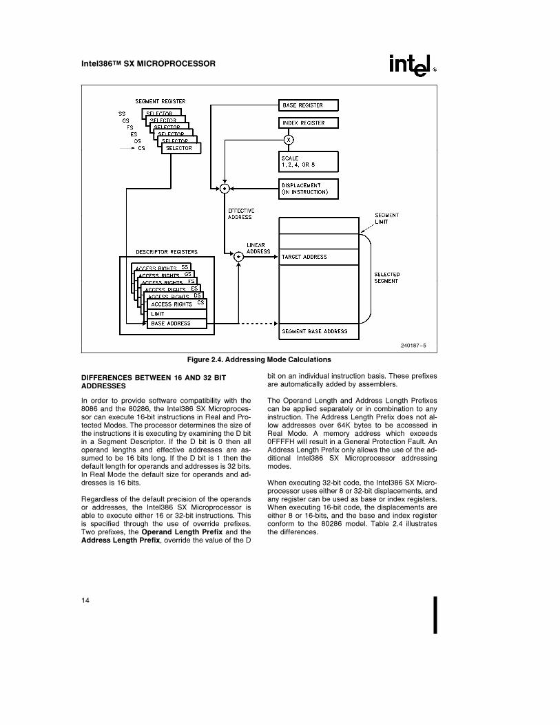
As shown in Figure 2.4, the effective address (EA) ofan operand is calculated according to the followingformula:
EA e BaseRegister a (IndexRegister*scaling)
a Displacement
1. Direct Mode: The operand’s offset is containedas part of the instruction as an 8, 16 or 32-bitdisplacement.
2. Register Indirect Mode: A BASE register con-tains the address of the operand.
3. Based Mode: A BASE register’s contents areadded to a DISPLACEMENT to form the oper-and’s offset.
4. Scaled Index Mode: An INDEX register’s con-tents are multiplied by a SCALING factor, and theresult is added to a DISPLACEMENT to form theoperand’s offset.
5. Based Scaled Index Mode: The contents of anINDEX register are multiplied by a SCALING fac-tor, and the result is added to the contents of aBASE register to obtain the operand’s offset.
6. Based Scaled Index Mode with Displacement:The contents of an INDEX register are multipliedby a SCALING factor, and the result is added tothe contents of a BASE register and a DISPLACE-MENT to form the operand’s offset.
13
Intel386TM SX MICROPROCESSOR
240187–5
Figure 2.4. Addressing Mode Calculations
DIFFERENCES BETWEEN 16 AND 32 BITADDRESSES
In order to provide software compatibility with the8086 and the 80286, the Intel386 SX Microproces-sor can execute 16-bit instructions in Real and Pro-tected Modes. The processor determines the size ofthe instructions it is executing by examining the D bitin a Segment Descriptor. If the D bit is 0 then alloperand lengths and effective addresses are as-sumed to be 16 bits long. If the D bit is 1 then thedefault length for operands and addresses is 32 bits.In Real Mode the default size for operands and ad-dresses is 16 bits.
Regardless of the default precision of the operandsor addresses, the Intel386 SX Microprocessor isable to execute either 16 or 32-bit instructions. Thisis specified through the use of override prefixes.Two prefixes, the Operand Length Prefix and theAddress Length Prefix, override the value of the D
bit on an individual instruction basis. These prefixesare automatically added by assemblers.
The Operand Length and Address Length Prefixescan be applied separately or in combination to anyinstruction. The Address Length Prefix does not al-low addresses over 64K bytes to be accessed inReal Mode. A memory address which exceeds0FFFFH will result in a General Protection Fault. AnAddress Length Prefix only allows the use of the ad-ditional Intel386 SX Microprocessor addressingmodes.
When executing 32-bit code, the Intel386 SX Micro-processor uses either 8 or 32-bit displacements, andany register can be used as base or index registers.When executing 16-bit code, the displacements areeither 8 or 16-bits, and the base and index registerconform to the 80286 model. Table 2.4 illustratesthe differences.
14

Intel386TM SX MICROPROCESSOR
Table 2.4. BASE and INDEX Registers for 16- and 32-Bit Addresses
16-Bit Addressing 32-Bit Addressing
BASE REGISTER BX,BP Any 32-bit GP Register
INDEX REGISTER SI,DI Any 32-bit GP Register
Except ESP
SCALE FACTOR None 1, 2, 4, 8
DISPLACEMENT 0, 8, 16-bits 0, 8, 32-bits
2.5 Data Types
The Intel386 SX Microprocessor supports all of thedata types commonly used in high level languages:
Bit: A single bit quantity.
Bit Field: A group of up to 32 contiguous bits, whichspans a maximum of four bytes.
Bit String: A set of contiguous bits; on the Intel386SX Microprocessor, bit strings can be up to 4 giga-bits long.
Byte: A signed 8-bit quantity.
Unsigned Byte: An unsigned 8-bit quantity.
Integer (Word): A signed 16-bit quantity.
Long Integer (Double Word): A signed 32-bit quan-tity. All operations assume a 2’s complement repre-sentation.
Unsigned Integer (Word): An unsigned 16-bitquantity.
Unsigned Long Integer (Double Word): An un-signed 32-bit quantity.
Signed Quad Word: A signed 64-bit quantity.
Unsigned Quad Word: An unsigned 64-bit quantity.
Pointer: A 16 or 32-bit offset-only quantity which in-directly references another memory location.
Long Pointer: A full pointer which consists of a 16-bit segment selector and either a 16 or 32-bit offset.
Char: A byte representation of an ASCII Alphanu-meric or control character.
String: A contiguous sequence of bytes, words ordwords. A string may contain between 1 byte and 4gigabytes.
BCD: A byte (unpacked) representation of decimaldigits 0–9.
Packed BCD: A byte (packed) representation of twodecimal digits 0–9 storing one digit in each nibble.
When the Intel386 SX Microprocessor is coupledwith its numerics coprocessor, the Intel387 SX, thenthe following common floating point types are sup-ported:
Floating Point: A signed 32, 64, or 80-bit real num-ber representation. Floating point numbers are sup-ported by the Intel387 SX numerics coprocessor.
Figure 2.5 illustrates the data types supported by theIntel386 SX Microprocessor and the Intel387 SX.
2.6 I/O Space
The Intel386 SX Microprocessor has two distinctphysical address spaces: physical memory and I/O.Generally, peripherals are placed in I/O space al-though the Intel386 SX Microprocessor also sup-ports memory-mapped peripherals. The I/O spaceconsists of 64K bytes which can be divided into 64K8-bit ports or 32K 16-bit ports, or any combination ofports which add up to no more than 64K bytes. The64K I/O address space refers to physical addressesrather than linear addresses since I/O instructionsdo not go through the segmentation or paging hard-ware. The M/IOÝ pin acts as an additional addressline, thus allowing the system designer to easily de-termine which address space the processor is ac-cessing.
The I/O ports are accessed by the IN and OUT in-structions, with the port address supplied as an im-mediate 8-bit constant in the instruction or in the DXregister. All 8-bit and 16-bit port addresses are zeroextended on the upper address lines. The I/O in-structions cause the M/IOÝ pin to be driven LOW.I/O port addresses 00F8H through 00FFH are re-served for use by Intel.
15

Intel386TM SX MICROPROCESSOR
240187–6
Figure 2.5. Intel386TM SX Microprocessor Supported Data Types
16

Intel386TM SX MICROPROCESSOR
2.7 Interrupts and Exceptions
Interrupts and exceptions alter the normal programflow in order to handle external events, report errorsor exceptional conditions. The difference betweeninterrupts and exceptions is that interrupts are usedto handle asynchronous external events while ex-ceptions handle instruction faults. Although a pro-gram can generate a software interrupt via an INT Ninstruction, the processor treats software interruptsas exceptions.
Hardware interrupts occur as the result of an exter-nal event and are classified into two types: maskableor non-maskable. Interrupts are serviced after theexecution of the current instruction. After the inter-rupt handler is finished servicing the interrupt, exe-cution proceeds with the instruction immediatelyafter the interrupted instruction.
Exceptions are classified as faults, traps, or aborts,depending on the way they are reported and wheth-er or not restart of the instruction causing the excep-tion is supported. Faults are exceptions that are de-tected and serviced before the execution of thefaulting instruction. Traps are exceptions that arereported immediately after the execution of the in-struction which caused the problem. Aborts are ex-ceptions which do not permit the precise location ofthe instruction causing the exception to be deter-mined.
Thus, when an interrupt service routine has beencompleted, execution proceeds from the instructionimmediately following the interrupted instruction. Onthe other hand, the return address from an excep-tion fault routine will always point to the instructioncausing the exception and will include any leadinginstruction prefixes. Table 2.5 summarizes the possi-ble interrupts for the Intel386 SX Microprocessorand shows where the return address points to.
Table 2.5. Interrupt Vector Assignments
Return Address
InterruptInstruction Which
Points toFunction
NumberCan Cause
FaultingType
ExceptionInstruction
Divide Error 0 DIV, IDIV YES FAULT
Debug Exception 1 any instruction YES TRAP*
NMI Interrupt 2 INT 2 or NMI NO NMI
One Byte Interrupt 3 INT NO TRAP
Interrupt on Overflow 4 INTO NO TRAP
Array Bounds Check 5 BOUND YES FAULT
Invalid OP-Code 6 Any illegal instruction YES FAULT
Device Not Available 7 ESC, WAIT YES FAULT
Double Fault 8Any instruction that can
ABORTgenerate an exception
Coprocessor Segment Overrun 9 ESC NO ABORT
Invalid TSS 10 JMP, CALL, IRET, INT YES FAULT
Segment Not Present 11 Segment Register Instructions YES FAULT
Stack Fault 12 Stack References YES FAULT
General Protection Fault 13 Any Memory Reference YES FAULT
Page Fault 14 Any Memory Access or Code Fetch YES FAULT
Coprocessor Error 16 ESC, WAIT YES FAULT
Intel Reserved 17–32
Two Byte Interrupt 33–255 INT n NO TRAP
*Some debug exceptions may report both traps on the previous instruction and faults on the next instruction.
17

Intel386TM SX MICROPROCESSOR
The Intel386 SX Microprocessor has the ability tohandle up to 256 different interrupts/exceptions. Inorder to service the interrupts, a table with up to 256interrupt vectors must be defined. The interrupt vec-tors are simply pointers to the appropriate interruptservice routine. In Real Mode, the vectors are 4-bytequantities, a Code Segment plus a 16-bit offset; inProtected Mode, the interrupt vectors are 8 bytequantities, which are put in an Interrupt DescriptorTable. Of the 256 possible interrupts, 32 are re-served for use by Intel and the remaining 224 arefree to be used by the system designer.
INTERRUPT PROCESSING
When an interrupt occurs, the following actions hap-pen. First, the current program address and Flagsare saved on the stack to allow resumption of theinterrupted program. Next, an 8-bit vector is suppliedto the Intel386 SX Microprocessor which identifiesthe appropriate entry in the interrupt table. The tablecontains the starting address of the interrupt serviceroutine. Then, the user supplied interrupt serviceroutine is executed. Finally, when an IRET instruc-tion is executed the old processor state is restoredand program execution resumes at the appropriateinstruction.
The 8-bit interrupt vector is supplied to the Intel386SX Microprocessor in several different ways: excep-tions supply the interrupt vector internally; softwareINT instructions contain or imply the vector; maska-ble hardware interrupts supply the 8-bit vector viathe interrupt acknowledge bus sequence. Non-Maskable hardware interrupts are assigned to inter-rupt vector 2.
Maskable Interrupt
Maskable interrupts are the most common way torespond to asynchronous external hardware events.A hardware interrupt occurs when the INTR is pulledHIGH and the Interrupt Flag bit (IF) is enabled. Theprocessor only responds to interrupts between in-structions (string instructions have an ‘interrupt win-dow‘ between memory moves which allows inter-rupts during long string moves). When an interruptoccurs the processor reads an 8-bit vector suppliedby the hardware which identifies the source of theinterrupt (one of 224 user defined interrupts).
Interrupts through interrupt gates automatically resetIF, disabling INTR requests. Interrupts through TrapGates leave the state of the IF bit unchanged. Inter-rupts through a Task Gate change the IF bit accord-ing to the image of the EFLAGs register in the task’sTask State Segment (TSS). When an IRET instruc-tion is executed, the original state of the IF bit isrestored.
Non-Maskable Interrupt
Non-maskable interrupts provide a method of servic-ing very high priority interrupts. When the NMI inputis pulled HIGH it causes an interrupt with an internal-ly supplied vector value of 2. Unlike a normal hard-ware interrupt, no interrupt acknowledgment se-quence is performed for an NMI.
While executing the NMI servicing procedure, the In-tel386 SX Microprocessor will not service any furtherNMI request or INT requests until an interrupt return(IRET) instruction is executed or the processor isreset. If NMI occurs while currently servicing an NMI,its presence will be saved for servicing after execut-ing the first IRET instruction. The IF bit is cleared atthe beginning of an NMI interrupt to inhibit furtherINTR interrupts.
Software Interrupts
A third type of interrupt/exception for the Intel386SX Microprocessor is the software interrupt. An INTn instruction causes the processor to execute theinterrupt service routine pointed to by the nth vectorin the interrupt table.
A special case of the two byte software interrupt INTn is the one byte INT 3, or breakpoint interrupt. Byinserting this one byte instruction in a program, theuser can set breakpoints in his program as a debug-ging tool.
A final type of software interrupt is the single stepinterrupt. It is discussed in Single Step Trap.
18
Intel386TM SX MICROPROCESSOR
INTERRUPT AND EXCEPTION PRIORITIES
Interrupts are externally generated events. Maska-ble Interrupts (on the INTR input) and Non-MaskableInterrupts (on the NMI input) are recognized at in-struction boundaries. When NMI and maskableINTR are both recognized at the same instructionboundary, the Intel386 SX Microprocessor invokesthe NMI service routine first. If maskable interruptsare still enabled after the NMI service routine hasbeen invoked, then the Intel386 SX Microprocessorwill invoke the appropriate interrupt service routine.
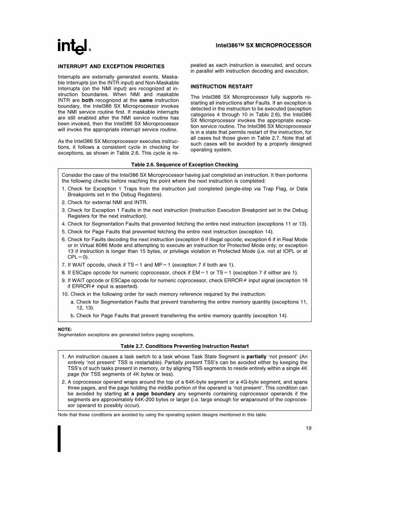
As the Intel386 SX Microprocessor executes instruc-tions, it follows a consistent cycle in checking forexceptions, as shown in Table 2.6. This cycle is re-
peated as each instruction is executed, and occursin parallel with instruction decoding and execution.
INSTRUCTION RESTART
The Intel386 SX Microprocessor fully supports re-starting all instructions after Faults. If an exception isdetected in the instruction to be executed (exceptioncategories 4 through 10 in Table 2.6), the Intel386SX Microprocessor invokes the appropriate excep-tion service routine. The Intel386 SX Microprocessoris in a state that permits restart of the instruction, forall cases but those given in Table 2.7. Note that allsuch cases will be avoided by a properly designedoperating system.
Table 2.6. Sequence of Exception Checking
Consider the case of the Intel386 SX Microprocessor having just completed an instruction. It then performsthe following checks before reaching the point where the next instruction is completed:
1. Check for Exception 1 Traps from the instruction just completed (single-step via Trap Flag, or DataBreakpoints set in the Debug Registers).
2. Check for external NMI and INTR.
3. Check for Exception 1 Faults in the next instruction (Instruction Execution Breakpoint set in the DebugRegisters for the next instruction).
4. Check for Segmentation Faults that prevented fetching the entire next instruction (exceptions 11 or 13).
5. Check for Page Faults that prevented fetching the entire next instruction (exception 14).
6. Check for Faults decoding the next instruction (exception 6 if illegal opcode; exception 6 if in Real Modeor in Virtual 8086 Mode and attempting to execute an instruction for Protected Mode only; or exception13 if instruction is longer than 15 bytes, or privilege violation in Protected Mode (i.e. not at IOPL or atCPLe0).
7. If WAIT opcode, check if TSe1 and MPe1 (exception 7 if both are 1).
8. If ESCape opcode for numeric coprocessor, check if EMe1 or TSe1 (exception 7 if either are 1).
9. If WAIT opcode or ESCape opcode for numeric coprocessor, check ERRORÝ input signal (exception 16if ERRORÝ input is asserted).
10. Check in the following order for each memory reference required by the instruction:
a. Check for Segmentation Faults that prevent transferring the entire memory quantity (exceptions 11,12, 13).
b. Check for Page Faults that prevent transferring the entire memory quantity (exception 14).
NOTE:Segmentation exceptions are generated before paging exceptions.
Table 2.7. Conditions Preventing Instruction Restart
1. An instruction causes a task switch to a task whose Task State Segment is partially ‘not present‘ (Anentirely ‘not present‘ TSS is restartable). Partially present TSS’s can be avoided either by keeping theTSS’s of such tasks present in memory, or by aligning TSS segments to reside entirely within a single 4Kpage (for TSS segments of 4K bytes or less).
2. A coprocessor operand wraps around the top of a 64K-byte segment or a 4G-byte segment, and spansthree pages, and the page holding the middle portion of the operand is ‘not present‘. This condition canbe avoided by starting at a page boundary any segments containing coprocessor operands if thesegments are approximately 64K-200 bytes or larger (i.e. large enough for wraparound of the coproces-sor operand to possibly occur).
Note that these conditions are avoided by using the operating system designs mentioned in this table.
19

Intel386TM SX MICROPROCESSOR
Table 2.8. Register Values after Reset
Flag Word (EFLAGS) uuuu0002H Note 1
Machine Status Word (CR0) uuuuuu10H
Instruction Pointer (EIP) 0000FFF0H
Code Segment (CS) F000H Note 2
Data Segment (DS) 0000H Note 3
Stack Segment (SS) 0000H
Extra Segment (ES) 0000H Note 3
Extra Segment (FS) 0000H
Extra Segment (GS) 0000H
EAX register 0000H Note 4
EDX register component and stepping ID Note 5
All other registers undefined Note 6
NOTES:1. EFLAG Register. The upper 14 bits of the EFLAGS register are undefined, all defined flag bits are zero.2. The Code Segment Register (CS) will have its Base Address set to 0FFFF0000H and Limit set to 0FFFFH.3. The Data and Extra Segment Registers (DS, ES) will have their Base Address set to 000000000H and Limit set to0FFFFH.4. If self-test is selected, the EAX register should contain a 0 value. If a value of 0 is not found then the self-test hasdetected a flaw in the part.5. EDX register always holds component and stepping identifier.6. All undefined bits are Intel Reserved and should not be used.
DOUBLE FAULT
A Double Fault (exception 8) results when the proc-essor attempts to invoke an exception service rou-tine for the segment exceptions (10, 11, 12 or 13),but in the process of doing so detects an exceptionother than a Page Fault (exception 14).
One other cause of generating a Double Fault is theIntel386 SX Microprocessor detecting any other ex-ception when it is attempting to invoke the PageFault (exception 14) service routine (for example, if aPage Fault is detected when the Intel386 SX Micro-processor attempts to invoke the Page Fault serviceroutine). Of course, in any functional system, notonly in Intel386 SX Microprocessor-based systems,the entire page fault service routine must remain‘present‘ in memory.
2.8 Reset and Initialization
When the processor is initialized or Reset the regis-ters have the values shown in Table 2.8. The In-tel386 SX Microprocessor will then start executinginstructions near the top of physical memory, at lo-cation 0FFFFF0H. When the first IntersegmentJump or Call is executed, address lines A20–A23 willdrop LOW for CS-relative memory cycles, and theIntel386 SX Microprocessor will only execute in-structions in the lower one megabyte of physicalmemory. This allows the system designer to use ashadow ROM at the top of physical memory to ini-tialize the system and take care of Resets.
RESET forces the Intel386 SX Microprocessor toterminate all execution and local bus activity. No in-struction execution or bus activity will occur as longas Reset is active. Between 350 and 450 CLK2 peri-ods after Reset becomes inactive, the Intel386 SXMicroprocessor will start executing instructions atthe top of physical memory.
2.9 Testability
The Intel386 SX Microprocessor, like the Intel386Microprocessor, offers testability features which in-clude a self-test and direct access to the page trans-lation cache.
SELF-TEST
The Intel386 SX Microprocessor has the capabilityto perform a self-test. The self-test checks the func-tion of all of the Control ROM and most of the non-random logic of the part. Approximately one-half ofthe Intel386 SX Microprocessor can be tested duringself-test.
Self-Test is initiated on the Intel386 SX Microproces-sor when the RESET pin transitions from HIGH toLOW, and the BUSYÝ pin is LOW. The self-testtakes about 220 clocks, or approximately 33 millisec-onds with a 16 MHz Intel386 SX CPU. At the com-pletion of self-test the processor performs reset andbegins normal operation. The part has successfullypassed self-test if the contents of the EAX are zero.If the results of the EAX are not zero then the self-test has detected a flaw in the part.
20

Intel386TM SX MICROPROCESSOR
TLB TESTING
The Intel386 SX Microprocessor also provides amechanism for testing the Translation LookasideBuffer (TLB) if desired. This particular mechanismmay not be continued in the same way in futureprocessors.
There are two TLB testing operations: 1) writing en-tries into the TLB, and, 2) performing TLB lookups.Two Test Registers, shown in Figure 2.6, are provid-ed for the purpose of testing. TR6 is the ‘‘test com-mand register’’, and TR7 is the ‘‘test data register’’.For a more detailed explanation of testing the TLB,see the Intel386TM SX Microprocessor Program-mer’s Reference Manual.
2.10 Debugging Support
The Intel386 SX Microprocessor provides severalfeatures which simplify the debugging process. Thethree categories of on-chip debugging aids are:
1. The code execution breakpoint opcode (0CCH).
2. The single-step capability provided by the TF bitin the flag register.
3. The code and data breakpoint capability providedby the Debug Registers DR0–3, DR6, and DR7.
BREAKPOINT INSTRUCTION
A single-byte software interrupt (Int 3) breakpoint in-struction is available for use by software debuggers.
The breakpoint opcode is 0CCh, and generates anexception 3 trap when executed.
SINGLE-STEP TRAP
If the single-step flag (TF, bit 8) in the EFLAG regis-ter is found to be set at the end of an instruction, asingle-step exception occurs. The single-step ex-ception is auto vectored to exception number 1.
DEBUG REGISTERS
The Debug Registers are an advanced debuggingfeature of the Intel386 SX Microprocessor. They al-low data access breakpoints as well as code execu-tion breakpoints. Since the breakpoints are indicatedby on-chip registers, an instruction execution break-point can be placed in ROM code or in code sharedby several tasks, neither of which can be supportedby the INT 3 breakpoint opcode.
The Intel386 SX Microprocessor contains six DebugRegisters, consisting of four breakpoint address reg-isters and two breakpoint control registers. Initiallyafter reset, breakpoints are in the disabled state;therefore, no breakpoints will occur unless the de-bug registers are programmed. Breakpoints set up inthe Debug Registers are auto-vectored to exception1. Figure 2.7 shows the breakpoint status and con-trol registers.
240187–7
Figure 2.6. Test Registers
21

Intel386TM SX MICROPROCESSOR
240187–8
Figure 2.7. Debug Registers
3.0 REAL MODE ARCHITECTURE
When the processor is reset or powered up it is ini-tialized in Real Mode. Real Mode has the same basearchitecture as the 8086, but allows access to the32-bit register set of the Intel386 SX Microproces-sor. The addressing mechanism, memory size, andinterrupt handling are all identical to the Real Modeon the 80286.
The default operand size in Real Mode is 16 bits, asin the 8086. In order to use the 32-bit registers andaddressing modes, override prefixes must be used.In addition, the segment size on the Intel386 SX Mi-croprocessor in Real Mode is 64K bytes so 32-bitaddresses must have a value less then 0000FFFFH.The primary purpose of Real Mode is to set up theprocessor for Protected Mode operation.
3.1 Memory Addressing
In Real Mode the linear addresses are the same asphysical addresses (paging is not allowed). Physicaladdresses are formed in Real Mode by adding thecontents of the appropriate segment register whichis shifted left by four bits to an effective address.This addition results in a 20-bit physical address or a1 megabyte address space. Since segment registersare shifted left by 4 bits, Real Mode segments al-ways start on 16-byte boundaries.
All segments in Real Mode are exactly 64K byteslong, and may be read, written, or executed. TheIntel386 SX Microprocessor will generate an excep-tion 13 if a data operand or instruction fetch occurspast the end of a segment.
22

Intel386TM SX MICROPROCESSOR
Table 3.1. Exceptions in Real Mode
FunctionInterrupt Related Return
Number Instructions Address Location
Interrupt table limit 8 INT vector is not Before
too small within table limit Instruction
CS, DS, ES, FS, GS 13 Word memory reference Before
Segment overrun exception with offset e 0FFFFH. Instruction
an attempt to execute
past the end of CS segment.
SS Segment overrun 12 Stack Reference Before
exception beyond offset e 0FFFFH Instruction
3.2 Reserved Locations
There are two fixed areas in memory which are re-served in Real address mode: the system initializa-tion area and the interrupt table area. Locations00000H through 003FFH are reserved for interruptvectors. Each one of the 256 possible interrupts hasa 4-byte jump vector reserved for it. Locations0FFFFF0H through 0FFFFFFH are reserved for sys-tem initialization.
3.3 Interrupts
Many of the exceptions discussed in section 2.7 arenot applicable to Real Mode operation; in particular,exceptions 10, 11 and 14 do not occur in RealMode. Other exceptions have slightly differentmeanings in Real Mode; Table 3.1 identifies theseexceptions.
3.4 Shutdown and Halt
The HLT instruction stops program execution andprevents the processor from using the local bus untilrestarted. Either NMI, FLTÝ, INTR with interruptsenabled (IFe1), or RESET will force the Intel386 SXMicroprocessor out of halt. If interrupted, the savedCS:IP will point to the next instruction after the HLT.
Shutdown will occur when a severe error is detectedthat prevents further processing. In Real Mode,shutdown can occur under two conditions:
1. An interrupt or an exception occurs (Exceptions 8or 13) and the interrupt vector is larger than theInterrupt Descriptor Table.
2. A CALL, INT or PUSH instruction attempts towrap around the stack segment when SP is noteven.
An NMI input can bring the processor out of shut-down if the Interrupt Descriptor Table limit is largeenough to contain the NMI interrupt vector (at least
000FH) and the stack has enough room to containthe vector and flag information (i.e. SP is greater that0005H). Otherwise, shutdown can only be exited bya processor reset.
3.5 LOCK Operation
The LOCK prefix on the Intel386 SX Microprocessor,even in Real Mode, is more restrictive than on the80286. This is due to the addition of paging on theIntel386 SX Microprocessor in Protected Mode andVirtual 8086 Mode. The LOCK prefix is not support-ed during repeat string instructions.
The only instruction forms where the LOCK prefix islegal on the Intel386 SX Microprocessor are shownin Table 3.2.
Table 3.2. Legal Instructions for the LOCK Prefix
OpcodeOperands
(Dest, Source)
BIT Test and
SET/RESET Mem, Reg/Immediate
/COMPLEMENT
XCHG Reg, Mem
XCHG Mem, Reg
ADD, OR, ADC, SBB,
AND, SUB, XOR Mem, Reg/Immediate
NOT, NEG, INC, DEC Mem
An exception 6 will be generated if a LOCK prefix isplaced before any instruction form or opcode notlisted above. The LOCK prefix allows indivisibleread/modify/write operations on memory operandsusing the instructions above.
The LOCK prefix is not IOPL-sensitive on theIntel386 SX Microprocessor. The LOCK prefix canbe used at any privilege level, but only on the in-struction forms listed in Table 3.2.
23

Intel386TM SX MICROPROCESSOR
4.0 PROTECTED MODEARCHITECTURE
The complete capabilities of the Intel386 SX Micro-processor are unlocked when the processor oper-ates in Protected Virtual Address Mode (ProtectedMode). Protected Mode vastly increases the linearaddress space to four gigabytes (232 bytes) and al-lows the running of virtual memory programs of al-most unlimited size (64 terabytes (246 bytes)). In ad-dition, Protected Mode allows the Intel386 SX Micro-processor to run all of the existing Intel386 DX CPU(using only 16 megabytes of physical memory),80286 and 8086 CPU’s software, while providing asophisticated memory management and a hard-ware-assisted protection mechanism. ProtectedMode allows the use of additional instructions spe-cially optimized for supporting multitasking operatingsystems. The base architecture of the Intel386 SXMicroprocessor remains the same; the registers, in-structions, and addressing modes described in theprevious sections are retained. The main differencebetween Protected Mode and Real Mode from aprogrammer’s viewpoint is the increased addressspace and a different addressing mechanism.
4.1 Addressing Mechanism
Like Real Mode, Protected Mode uses two compo-nents to form the logical address; a 16-bit selector isused to determine the linear base address of a seg-ment, the base address is added to a 32-bit effectiveaddress to form a 32-bit linear address. The linearaddress is then either used as a 24-bit physical ad-dress, or if paging is enabled the paging mechanismmaps the 32-bit linear address into a 24-bit physicaladdress.
The difference between the two modes lies in calcu-lating the base address. In Protected Mode, the se-lector is used to specify an index into an operatingsystem defined table (see Figure 4.1). The tablecontains the 32-bit base address of a given seg-ment. The physical address is formed by adding thebase address obtained from the table to the offset.
Paging provides an additional memory managementmechanism which operates only in Protected Mode.Paging provides a means of managing the very largesegments of the Intel386 SX Microprocessor, aspaging operates beneath segmentation. The pagemechanism translates the protected linear addresswhich comes from the segmentation unit into aphysical address. Figure 4.2 shows the complete In-tel386 SX Microprocessor addressing mechanismwith paging enabled.
4.2 Segmentation
Segmentation is one method of memory manage-ment. Segmentation provides the basis for protec-tion. Segments are used to encapsulate regions ofmemory which have common attributes. For exam-ple, all of the code of a given program could be con-tained in a segment, or an operating system tablemay reside in a segment. All information about eachsegment is stored in an 8 byte data structure calleda descriptor. All of the descriptors in a system arecontained in descriptor tables which are recognizedby hardware.
TERMINOLOGY
The following terms are used throughout the discus-sion of descriptors, privilege levels and protection:
PL: Privilege LevelÐOne of the four hierarchicalprivilege levels. Level 0 is the most privilegedlevel and level 3 is the least privileged.
RPL: Requestor Privilege LevelÐThe privilege levelof the original supplier of the selector. RPL isdetermined by the least two significant bits ofa selector.
DPL: Descriptor Privilege LevelÐThis is the leastprivileged level at which a task may accessthat descriptor (and the segment associatedwith that descriptor). Descriptor Privilege Lev-el is determined by bits 6:5 in the AccessRight Byte of a descriptor.
CPL: Current Privilege LevelÐThe privilege level atwhich a task is currently executing, whichequals the privilege level of the code segmentbeing executed. CPL can also be determinedby examining the lowest 2 bits of the CS regis-ter, except for conforming code segments.
EPL: Effective Privilege LevelÐThe effective privi-lege level is the least privileged of the RPLand the DPL. EPL is the numerical maximumof RPL and DPL.
Task: One instance of the execution of a program.Tasks are also referred to as processes.
DESCRIPTOR TABLES
The descriptor tables define all of the segmentswhich are used in a Intel386 SX Microprocessor sys-tem. There are three types of tables which hold de-scriptors: the Global Descriptor Table, Local De-scriptor Table, and the Interrupt Descriptor Table. Allof the tables are variable length memory arrays andcan vary in size from 8 bytes to 64K bytes. Eachtable can hold up to 8192 8-byte descriptors. Theupper 13 bits of a selector are used as an index intothe descriptor table. The tables have registers asso-ciated with them which hold the 32-bit linear baseaddress and the 16-bit limit of each table.
24

Intel386TM SX MICROPROCESSOR
240187–9
Figure 4.1. Protected Mode Addressing
240187–10
Figure 4.2. Paging and Segmentation
240187–11
Figure 4.3. Descriptor Table Registers
25
Intel386TM SX MICROPROCESSOR
Each of the tables has a register associated with it:GDTR, LDTR, and IDTR; see Figure 2.1. The LGDT,LLDT, and LIDT instructions load the base and limitof the Global, Local, and Interrupt Descriptor Tablesinto the appropriate register. The SGDT, SLDT, andSIDT store the base and limit values. These are priv-ileged instructions.
Global Descriptor Table
The Global Descriptor Table (GDT) contains de-scriptors which are available to all of the tasks in asystem. The GDT can contain any type of segmentdescriptor except for interrupt and trap descriptors.Every Intel386 SX CPU system contains a GDT.
The first slot of the Global Descriptor Table corre-sponds to the null selector and is not used. The nullselector defines a null pointer value.
Local Descriptor Table
LDTs contain descriptors which are associated witha given task. Generally, operating systems are de-signed so that each task has a separate LDT. TheLDT may contain only code, data, stack, task gate,and call gate descriptors. LDTs provide a mecha-nism for isolating a given task’s code and data seg-ments from the rest of the operating system, whilethe GDT contains descriptors for segments whichare common to all tasks. A segment cannot be ac-cessed by a task if its segment descriptor does notexist in either the current LDT or the GDT. This pro-vides both isolation and protection for a task’s seg-ments while still allowing global data to be sharedamong tasks.
Unlike the 6-byte GDT or IDT registers which containa base address and limit, the visible portion of theLDT register contains only a 16-bit selector. This se-lector refers to a Local Descriptor Table descriptor inthe GDT (see figure 2.1).
Interrupt Descriptor Table
The third table needed for Intel386 SX Microproces-sor systems is the Interrupt Descriptor Table. TheIDT contains the descriptors which point to the loca-tion of the up to 256 interrupt service routines. TheIDT may contain only task gates, interrupt gates, andtrap gates. The IDT should be at least 256 bytes insize in order to hold the descriptors for the 32 IntelReserved Interrupts. Every interrupt used by a sys-tem must have an entry in the IDT. The IDT entriesare referenced by INT instructions, external interruptvectors, and exceptions.
DESCRIPTORS
The object to which the segment selector points tois called a descriptor. Descriptors are eight bytequantities which contain attributes about a given re-gion of linear address space. These attributes in-clude the 32-bit base linear address of the segment,the 20-bit length and granularity of the segment, theprotection level, read, write or execute privileges,the default size of the operands (16-bit or 32-bit),and the type of segment. All of the attribute informa-tion about a segment is contained in 12 bits in thesegment descriptor. Figure 4.4 shows the generalformat of a descriptor. All segments on the Intel386SX Microprocessor have three attribute fields incommon: the P bit, the DPL bit, and the S bit. The P
31 0 BYTE
SEGMENT BASE 15 . . . 0 SEGMENT LIMIT 15 . . . 0ADDRESS
0
BASE 31 . . . 24 G D 0 AVLLIMIT
P DPL S TYPE ABASE
a419 . . . 16 23 . . . 16
BASE Base Address of the segmentLIMIT The length of the segmentP Present Bit 1ePresent 0eNot PresentDPL Descriptor Privilege Level 0–3S Segment Descriptor 0eSystem Descriptor 1eCode or Data Segment DescriptorTYPE Type of SegmentA Accessed BitG Granularity Bit 1eSegment length is page granular 0eSegment length is byte granularD Default Operation Size (recognized in code segment descriptors only) 1e32-bit segment 0e16-bit segment0 Bit must be zero (0) for compatibility with future processorsAVL Available field for user or OS
Figure 4.4. Segment Descriptors
26
Intel386TM SX MICROPROCESSOR
(Present) Bit is 1 if the segment is loaded in physicalmemory. If Pe0 then any attempt to access thissegment causes a not present exception (exception11). The Descriptor Privilege Level, DPL, is a two bitfield which specifies the protection level, 0–3, asso-ciated with a segment.
The Intel386 SX Microprocessor has two main cate-gories of segments: system segments and non-sys-tem segments (for code and data). The segment bit,S, determines if a given segment is a system seg-
ment or a code or data segment. If the S bit is 1 thenthe segment is either a code or data segment; if it is0 then the segment is a system segment.
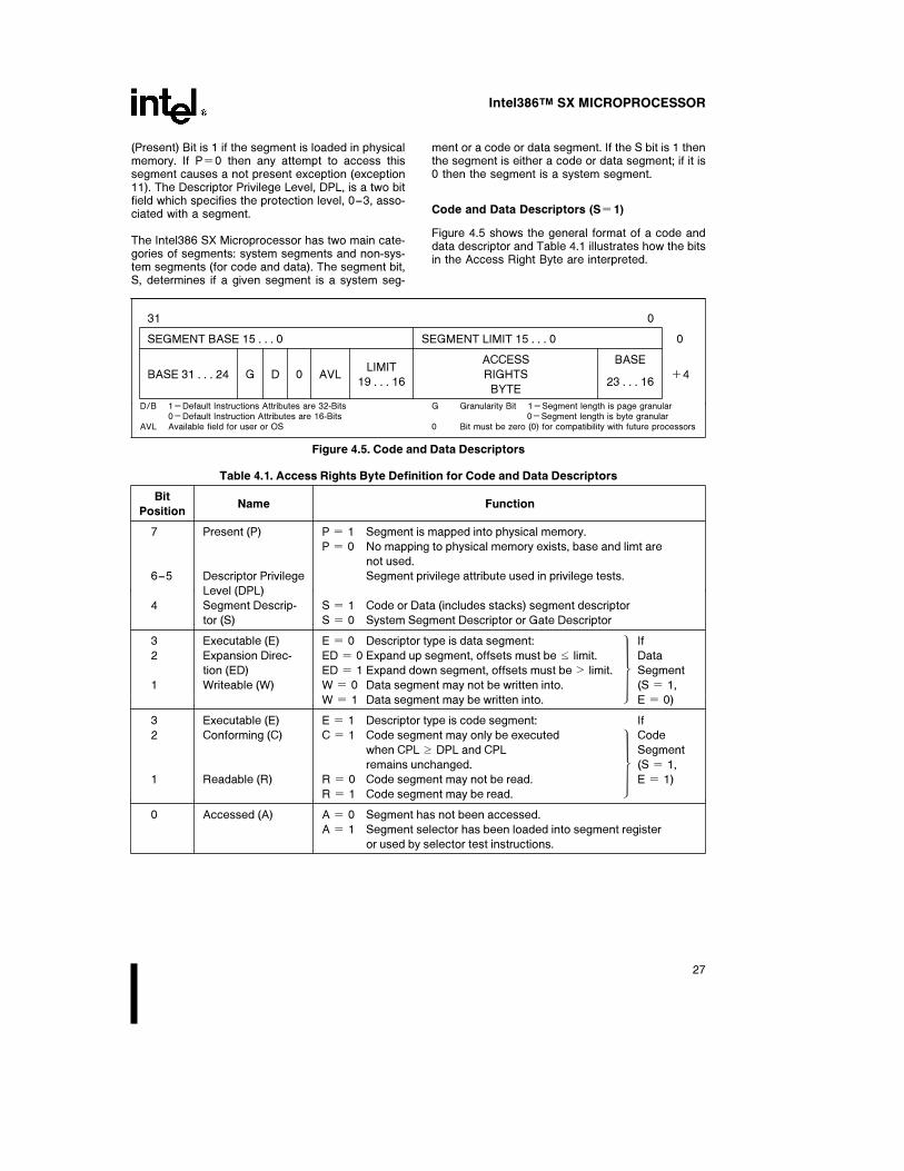
Code and Data Descriptors (Se1)
Figure 4.5 shows the general format of a code anddata descriptor and Table 4.1 illustrates how the bitsin the Access Right Byte are interpreted.
31 0
SEGMENT BASE 15 . . . 0 SEGMENT LIMIT 15 . . . 0 0
LIMITACCESS BASE
BASE 31 . . . 24 G D 0 AVL19 . . . 16
RIGHTS23 . . . 16
a4
BYTE
D/B 1eDefault Instructions Attributes are 32-Bits0eDefault Instruction Attributes are 16-Bits
AVL Available field for user or OS
G Granularity Bit 1eSegment length is page granular0eSegment length is byte granular
0 Bit must be zero (0) for compatibility with future processors
Figure 4.5. Code and Data Descriptors
Table 4.1. Access Rights Byte Definition for Code and Data Descriptors
BitName Function
Position
7 Present (P) P e 1 Segment is mapped into physical memory.
P e 0 No mapping to physical memory exists, base and limt are
not used.
6–5 Descriptor Privilege Segment privilege attribute used in privilege tests.
Level (DPL)
4 Segment Descrip- S e 1 Code or Data (includes stacks) segment descriptor
tor (S) S e 0 System Segment Descriptor or Gate Descriptor
3 Executable (E) E e 0 Descriptor type is data segment: If
2 Expansion Direc- ED e 0 Expand up segment, offsets must be s limit. Data
tion (ED) ED e 1 Expand down segment, offsets must be l limit. Segment
1 Writeable (W) W e 0 Data segment may not be written into. (S e 1,
W e 1 Data segment may be written into. * E e 0)
3 Executable (E) E e 1 Descriptor type is code segment: If
2 Conforming (C) C e 1 Code segment may only be executed Code
when CPL t DPL and CPL Segment
remains unchanged. (S e 1,
1 Readable (R) R e 0 Code segment may not be read. E e 1)
R e 1 Code segment may be read. *0 Accessed (A) A e 0 Segment has not been accessed.
A e 1 Segment selector has been loaded into segment register
or used by selector test instructions.
27

Intel386TM SX MICROPROCESSOR
31 16 0
SEGMENT BASE 15 . . . 0 SEGMENT LIMIT 15 . . . 0 0
BASE 31 . . . 24 G 0 0 0LIMIT
P DPL 0 TYPEBASE
a419 . . . 16 23 . . . 16
Type Defines
0 Invalid1 Available 80286 TSS2 LDT3 Busy 80286 TSS4 80286 Call Gate5 Task Gate (for 80286 or Intel386TM SX
Microprocessor Task)6 80286 Interrupt Gate7 80286 Trap Gate
Type Defines
8 Invalid9 Available Intel386TM SX Microprocessor TSSA Undefined (Intel Reserved)B Busy Intel386TM SX Microprocessor TSSC Intel386TM SX Microprocessor Call GateD Undefined (Intel Reserved)E Intel386TM SX Microprocessor Interrupt GateF Intel386TM SX Microprocessor Trap Gate
Figure 4.6. System Descriptors
Code and data segments have several descriptorfields in common. The accessed bit, A, is set when-ever the processor accesses a descriptor. The gran-ularity bit, G, specifies if a segment length is byte-granular or page-granular.
System Descriptor Formats (Se0)
System segments describe information about oper-ating system tables, tasks, and gates. Figure 4.6shows the general format of system segment de-scriptors, and the various types of system segments.Intel386 SX system descriptors (which are the sameas Intel386 DX CPU system descriptors) contain a32-bit base linear address and a 20-bit segment lim-it. 80286 system descriptors have a 24-bit base ad-dress and a 16-bit segment limit. 80286 system de-scriptors are identified by the upper 16 bits being allzero.
Differences Between Intel386TM SXMicroprocessor and 80286 Descriptors
In order to provide operating system compatibilitywith the 80286 the Intel386 SX CPU supports all ofthe 80286 segment descriptors. The 80286 systemsegment descriptors contain a 24-bit base addressand 16-bit limit, while the Intel386 SX CPU systemsegment descriptors have a 32-bit base address, a20-bit limit field, and a granularity bit. The word countfield specifies the number of 16-bit quantities to copyfor 80286 call gates and 32-bit quantities forIntel386 SX CPU call gates.
Selector Fields
A selector in Protected Mode has three fields: Localor Global Descriptor Table indicator (TI), DescriptorEntry Index (Index), and Requestor (the selector’s)Privilege Level (RPL) as shown in Figure 4.7. The TIbit selects either the Global Descriptor Table or theLocal Descriptor Table. The Index selects one of 8kdescriptors in the appropriate descriptor table. TheRPL bits allow high speed testing of the selector’sprivilege attributes.
Segment Descriptor Cache
In addition to the selector value, every segment reg-ister has a segment descriptor cache register asso-ciated with it. Whenever a segment register’s con-tents are changed, the 8-byte descriptor associatedwith that selector is automatically loaded (cached)on the chip. Once loaded, all references to that seg-ment use the cached descriptor information insteadof reaccessing the descriptor. The contents of thedescriptor cache are not visible to the programmer.Since descriptor caches only change when a seg-ment register is changed, programs which modifythe descriptor tables must reload the appropriatesegment registers after changing a descriptor’s val-ue.
28

Intel386TM SX MICROPROCESSOR
240187–12
Figure 4.7. Example Descriptor Selection
4.3 Protection
The Intel386 SX Microprocessor has four levels ofprotection which are optimized to support a multi-tasking operating system and to isolate and protectuser programs from each other and the operatingsystem. The privilege levels control the use of privi-leged instructions, I/O instructions, and access tosegments and segment descriptors. The Intel386 SXMicroprocessor also offers an additional type of pro-tection on a page basis when paging is enabled.
The four-level hierarchical privilege system is an ex-tension of the user/supervisor privilege mode com-monly used by minicomputers. The user/supervisormode is fully supported by the Intel386 SX Micro-processor paging mechanism. The privilege levels(PL) are numbered 0 through 3. Level 0 is the mostprivileged level.
RULES OF PRIVILEGE
The Intel386 SX Microprocessor controls access toboth data and procedures between levels of a task,according to the following rules.
Ð Data stored in a segment with privilege level pcan be accessed only by code executing at aprivilege level at least as privileged as p.
Ð A code segment/procedure with privilege level pcan only be called by a task executing at thesame or a lesser privilege level than p.
PRIVILEGE LEVELS
At any point in time, a task on the Intel386 SX Micro-processor always executes at one of the four privi-lege levels. The Current Privilege Level (CPL) speci-fies what the task’s privilege level is. A task’s CPLmay only be changed by control transfers throughgate descriptors to a code segment with a differentprivilege level. Thus, an application program runningat PLe3 may call an operating system routine atPLe1 (via a gate) which would cause the task’s CPLto be set to 1 until the operating system routine wasfinished.
Selector Privilege (RPL)
The privilege level of a selector is specified by theRPL field. The selector’s RPL is only used to estab-lish a less trusted privilege level than the currentprivilege level of the task for the use of a segment.This level is called the task’s effective privilege level(EPL). The EPL is defined as being the least privi-leged (numerically larger) level of a task’s CPL and aselector’s RPL. The RPL is most commonly used toverify that pointers passed to an operating systemprocedure do not access data that is of higher privi-lege than the procedure that originated the pointer.Since the originator of a selector can specify anyRPL value, the Adjust RPL (ARPL) instruction is pro-vided to force the RPL bits to the originator’s CPL.
29

Intel386TM SX MICROPROCESSOR
Table 4.2. Descriptor Types Used for Control Transfer
Control Transfer Types Operation TypesDescriptor Descriptor
Referenced Table
Intersegment within the same privilege level JMP, CALL RET, IRET* Code Segment GDT/LDT
Intersegment to the same or higher privilege level CALL Call Gate GDT/LDT
Interrupt within task may change CPLInterrupt instruction Trap or IDT
Exception External Interrupt
Interrupt Gate
Intersegment to a lower privilege level RET, IRET* Code Segment GDT/LDT
(changes task CPL)
CALL, JMP Task State GDT
Segment
Task Switch CALL, JMP Task Gate GDT/LDT
IRET** Task Gate IDT
Interrupt instruction,
Exception, External
Interrupt
*NT (Nested Task bit of flag register) e 0**NT (Nested Task bit of flag register) e 1
I/O Privilege
The I/O privilege level (IOPL) lets the operating sys-tem code executing at CPLe0 define the least privi-leged level at which I/O instructions can be used. Anexception 13 (General Protection Violation) is gener-ated if an I/O instruction is attempted when the CPLof the task is less privileged then the IOPL. TheIOPL is stored in bits 13 and 14 of the EFLAGS reg-ister. The following instructions cause an exception13 if the CPL is greater than IOPL: IN, INS, OUT,OUTS, STI, CLI, LOCK prefix.
Descriptor Access
There are basically two types of segment accesses:those involving code segments such as controltransfers, and those involving data accesses. Deter-mining the ability of a task to access a segment in-volves the type of segment to be accessed, the in-struction used, the type of descriptor used and CPL,RPL, and DPL as described above.
Any time an instruction loads a data segment regis-ter (DS, ES, FS, GS) the Intel386 SX Microprocessormakes protection validation checks. Selectors load-ed in the DS, ES, FS, GS registers must refer only todata segment or readable code segments.
Finally the privilege validation checks are performed.The CPL is compared to the EPL and if the EPL ismore privileged than the CPL, an exception 13 (gen-eral protection fault) is generated.
The rules regarding the stack segment are slightlydifferent than those involving data segments. In-structions that load selectors into SS must refer todata segment descriptors for writeable data seg-ments. The DPL and RPL must equal the CPL of allother descriptor types or a privilege level violationwill cause an exception 13. A stack not present faultcauses an exception 12.
PRIVILEGE LEVEL TRANSFERS
Inter-segment control transfers occur when a selec-tor is loaded in the CS register. For a typical systemmost of these transfers are simply the result of a callor a jump to another routine. There are five types ofcontrol transfers which are summarized in Table 4.2.Many of these transfers result in a privilege leveltransfer. Changing privilege levels is done only bycontrol transfers, using gates, task switches, and in-terrupt or trap gates.
Control transfers can only occur if the operationwhich loaded the selector references the correct de-scriptor type. Any violation of these descriptor usagerules will cause an exception 13.
30

Intel386TM SX MICROPROCESSOR
240187–13
Type e 9: Available Intel386TM SX Microprocessor TSS.Type e B: Busy Intel386 SX Microprocessor TSS.
Figure 4.8. Intel386TM SX Microprocessor TSS and TSS Registers
31
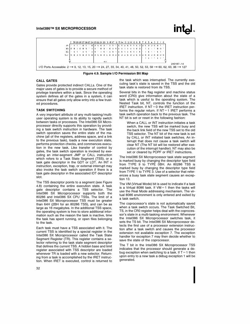
Intel386TM SX MICROPROCESSOR
240187–14
I/O Ports Accessible: 2x9, 12, 13, 15, 20x24, 27, 33, 34, 40, 41, 48, 50, 52, 53, 58x60, 62, 63, 96x127
Figure 4.9. Sample I/O Permission Bit Map
CALL GATES
Gates provide protected indirect CALLs. One of themajor uses of gates is to provide a secure method ofprivilege transfers within a task. Since the operatingsystem defines all of the gates in a system, it canensure that all gates only allow entry into a few trust-ed procedures.
TASK SWITCHING
A very important attribute of any multi-tasking/multi-user operating system is its ability to rapidly switchbetween tasks or processes. The Intel386 SX Micro-processor directly supports this operation by provid-ing a task switch instruction in hardware. The taskswitch operation saves the entire state of the ma-chine (all of the registers, address space, and a linkto the previous task), loads a new execution state,performs protection checks, and commences execu-tion in the new task. Like transfer of control bygates, the task switch operation is invoked by exe-cuting an inter-segment JMP or CALL instructionwhich refers to a Task State Segment (TSS), or atask gate descriptor in the GDT or LDT. An INT ninstruction, exception, trap, or external interrupt mayalso invoke the task switch operation if there is atask gate descriptor in the associated IDT descriptorslot.
The TSS descriptor points to a segment (see Figure4.8) containing the entire execution state. A taskgate descriptor contains a TSS selector. TheIntel386 SX Microprocessor supports both the80286 and Intel386 SX CPU TSSs. The limit of aIntel386 SX Microprocessor TSS must be greaterthan 64H (2BH for an 80286 TSS), and can be aslarge as 16 megabytes. In the additional TSS space,the operating system is free to store additional infor-mation such as the reason the task is inactive, timethe task has spent running, or open files belongingto the task.
Each task must have a TSS associated with it. Thecurrent TSS is identified by a special register in theIntel386 SX Microprocessor called the Task StateSegment Register (TR). This register contains a se-lector referring to the task state segment descriptorthat defines the current TSS. A hidden base and limitregister associated with TSS descriptor are loadedwhenever TR is loaded with a new selector. Return-ing from a task is accomplished by the IRET instruc-tion. When IRET is executed, control is returned to
the task which was interrupted. The currently exe-cuting task’s state is saved in the TSS and the oldtask state is restored from its TSS.
Several bits in the flag register and machine statusword (CR0) give information about the state of atask which is useful to the operating system. TheNested Task bit, NT, controls the function of theIRET instruction. If NTe0 the IRET instruction per-forms the regular return. If NTe1 IRET performs atask switch operation back to the previous task. TheNT bit is set or reset in the following fashion:
When a CALL or INT instruction initiates a taskswitch, the new TSS will be marked busy andthe back link field of the new TSS set to the oldTSS selector. The NT bit of the new task is setby CALL or INT initiated task switches. An in-terrupt that does not cause a task switch willclear NT (The NT bit will be restored after exe-cution of the interrupt handler). NT may also beset or cleared by POPF or IRET instructions.
The Intel386 SX Microprocessor task state segmentis marked busy by changing the descriptor type fieldfrom TYPE 9 to TYPE 0BH. An 80286 TSS ismarked busy by changing the descriptor type fieldfrom TYPE 1 to TYPE 3. Use of a selector that refer-ences a busy task state segment causes an excep-tion 13.
The VM (Virtual Mode) bit is used to indicate if a taskis a Virtual 8086 task. If VMe1 then the tasks willuse the Real Mode addressing mechanism. The vir-tual 8086 environment is only entered and exited bya task switch.
The coprocessor’s state is not automatically savedwhen a task switch occurs. The Task Switched Bit,TS, in the CR0 register helps deal with the coproces-sor’s state in a multi-tasking environment. Wheneverthe Intel386 SX Microprocessor switches task, itsets the TS bit. The Intel386 SX Microprocessor de-tects the first use of a processor extension instruc-tion after a task switch and causes the processorextension not available exception 7. The exceptionhandler for exception 7 may then decide whether tosave the state of the coprocessor.
The T bit in the Intel386 SX Microprocessor TSSindicates that the processor should generate a de-bug exception when switching to a task. If Te1 thenupon entry to a new task a debug exception 1 will begenerated.
32
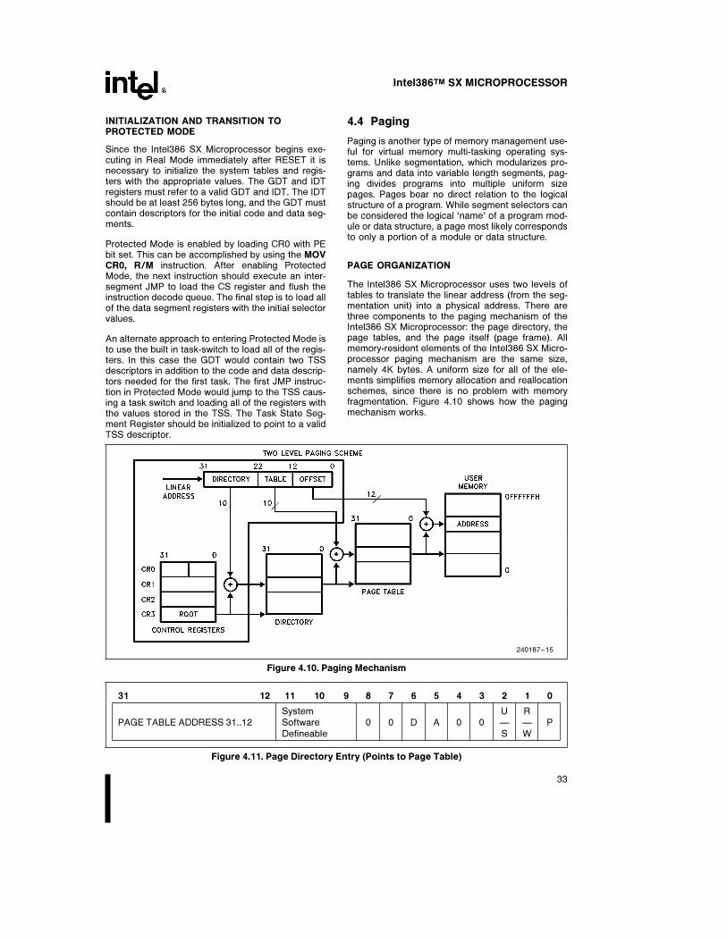
Intel386TM SX MICROPROCESSOR
INITIALIZATION AND TRANSITION TOPROTECTED MODE
Since the Intel386 SX Microprocessor begins exe-cuting in Real Mode immediately after RESET it isnecessary to initialize the system tables and regis-ters with the appropriate values. The GDT and IDTregisters must refer to a valid GDT and IDT. The IDTshould be at least 256 bytes long, and the GDT mustcontain descriptors for the initial code and data seg-ments.
Protected Mode is enabled by loading CR0 with PEbit set. This can be accomplished by using the MOVCR0, R/M instruction. After enabling ProtectedMode, the next instruction should execute an inter-segment JMP to load the CS register and flush theinstruction decode queue. The final step is to load allof the data segment registers with the initial selectorvalues.
An alternate approach to entering Protected Mode isto use the built in task-switch to load all of the regis-ters. In this case the GDT would contain two TSSdescriptors in addition to the code and data descrip-tors needed for the first task. The first JMP instruc-tion in Protected Mode would jump to the TSS caus-ing a task switch and loading all of the registers withthe values stored in the TSS. The Task State Seg-ment Register should be initialized to point to a validTSS descriptor.
4.4 Paging
Paging is another type of memory management use-ful for virtual memory multi-tasking operating sys-tems. Unlike segmentation, which modularizes pro-grams and data into variable length segments, pag-ing divides programs into multiple uniform sizepages. Pages bear no direct relation to the logicalstructure of a program. While segment selectors canbe considered the logical ‘name‘ of a program mod-ule or data structure, a page most likely correspondsto only a portion of a module or data structure.
PAGE ORGANIZATION
The Intel386 SX Microprocessor uses two levels oftables to translate the linear address (from the seg-mentation unit) into a physical address. There arethree components to the paging mechanism of theIntel386 SX Microprocessor: the page directory, thepage tables, and the page itself (page frame). Allmemory-resident elements of the Intel386 SX Micro-processor paging mechanism are the same size,namely 4K bytes. A uniform size for all of the ele-ments simplifies memory allocation and reallocationschemes, since there is no problem with memoryfragmentation. Figure 4.10 shows how the pagingmechanism works.
240187–15
Figure 4.10. Paging Mechanism
31 12 11 10 9 8 7 6 5 4 3 2 1 0
System U RPAGE TABLE ADDRESS 31..12 Software 0 0 D A 0 0 Ð Ð P
Defineable S W
Figure 4.11. Page Directory Entry (Points to Page Table)
33

Intel386TM SX MICROPROCESSOR
31 12 11 10 9 8 7 6 5 4 3 2 1 0
System U RPAGE FRAME ADDRESS 31..12 Software 0 0 D A 0 0 Ð Ð P
Defineable S W
Figure 4.12. Page Table Entry (Points to Page)
Page Fault Register
CR2 is the Page Fault Linear Address register. Itholds the 32-bit linear address which caused the lastPage Fault detected.
Page Descriptor Base Register
CR3 is the Page Directory Physical Base AddressRegister. It contains the physical starting address ofthe Page Directory (this value is truncated to a 24-bitvalue associated with the Intel386 SX CPU’s 16megabyte physical memory limitation). The lower 12bits of CR3 are always zero to ensure that the PageDirectory is always page aligned. Loading it with aMOV CR3, reg instruction causes the page table en-try cache to be flushed, as will a task switch througha TSS which changes the value of CR0.
Page Directory
The Page Directory is 4k bytes long and allows up to1024 page directory entries. Each page directory en-try contains information about the page table andthe address of the next level of tables, the PageTables. The contents of a Page Directory Entry areshown in figure 4.11. The upper 10 bits of the linearaddress (A31–A22) are used as an index to selectthe correct Page Directory Entry.
The page table address contains the upper 20 bitsof a 32-bit physical address that is used as the baseaddress for the next set of tables, the page tables.The lower 12 bits of the page table address are zeroso that the page table addresses appear on 4 kbyteboundaries. For a Intel386 DX CPU system the up-per 20 bits will select one of 220 page tables, but fora Intel386 SX Microprocessor system the upper 20bits only select one of 212 page tables. Again, this isbecause the Intel386 SX Microprocessor is limited toa 24-bit physical address and the upper 8 bits (A24–A31) are truncated when the address is output on its24 address pins.
Page Tables
Each Page Table is 4K bytes long and allows up to1024 Page table Entries. Each page table entry con-tains information about the Page Frame and its ad-
dress. The contents of a Page Table Entry areshown in figure 4.12. The middle 10 bits of the linearaddress (A21–A12) are used as an index to selectthe correct Page Table Entry.
The Page Frame Address contains the upper 20 bitsof a 32-bit physical address that is used as the baseaddress for the Page Frame. The lower 12 bits of thePage Frame Address are zero so that the PageFrame addresses appear on 4 kbyte boundaries. Foran Intel386 DX CPU system the upper 20 bits willselect one of 220 Page Frames, but for anIntel386 SX Microprocessor system the upper 20bits only select one of 212 Page Frames. Again, thisis because the Intel386 SX Microprocessor is limitedto a 24-bit physical address space and the upper 8bits (A24–A31) are truncated when the address isoutput on its 24 address pins.
Page Directory/Table Entries
The lower 12 bits of the Page Table Entries andPage Directory Entries contain statistical informationabout pages and page tables respectively. The P(Present) bit indicates if a Page Directory or PageTable entry can be used in address translation. IfPe1, the entry can be used for address translation.If Pe0, the entry cannot be used for translation. Allof the other bits are available for use by the soft-ware. For example, the remaining 31 bits could beused to indicate where on disk the page is stored.
The A (Accessed) bit is set by the Intel386 SX CPUfor both types of entries before a read or write ac-cess occurs to an address covered by the entry. TheD (Dirty) bit is set to 1 before a write to an addresscovered by that page table entry occurs. The D bit isundefined for Page Directory Entries. When the P, Aand D bits are updated by the Intel386 SX CPU, theprocessor generates a Read- Modify-Write cyclewhich locks the bus and prevents conflicts with oth-er processors or peripherals. Software which modi-fies these bits should use the LOCK prefix to ensurethe integrity of the page tables in multi-master sys-tems.
The 3 bits marked system software definable in Fig-ures 4.11 and Figure 4.12 are software definable.System software writers are free to use these bitsfor whatever purpose they wish.
34

Intel386TM SX MICROPROCESSOR
PAGE LEVEL PROTECTION (R/W, U/S BITS)
The Intel386 SX Microprocessor provides a set ofprotection attributes for paging systems. The pagingmechanism distinguishes between two levels of pro-tection: User, which corresponds to level 3 of thesegmentation based protection, and supervisorwhich encompasses all of the other protection levels(0, 1, 2). Programs executing at Level 0, 1 or 2 by-pass the page protection, although segmentation-based protection is still enforced by the hardware.
The U/S and R/W bits are used to provide User/Su-pervisor and Read/Write protection for individualpages or for all pages covered by a Page Table Di-rectory Entry. The U/S and R/W bits in the secondlevel Page Table Entry apply only to the page de-scribed by that entry. While the U/S and R/W bits inthe first level Page Directory Table apply to all pagesdescribed by the page table pointed to by that direc-tory entry. The U/S and R/W bits for a given pageare obtained by taking the most restrictive of theU/S and R/W from the Page Directory Table Entriesand using these bits to address the page.
TRANSLATION LOOKASIDE BUFFER
The Intel386 SX Microprocessor paging hardware isdesigned to support demand paged virtual memorysystems. However, performance would degradesubstantially if the processor was required to accesstwo levels of tables for every memory reference. Tosolve this problem, the Intel386 SX Microprocessorkeeps a cache of the most recently accessed pages,this cache is called the Translation Lookaside Buffer(TLB). The TLB is a four-way set associative 32-en-try page table cache. It automatically keeps the mostcommonly used page table entries in the processor.The 32-entry TLB coupled with a 4K page size re-sults in coverage of 128K bytes of memory address-es. For many common multi-tasking systems, theTLB will have a hit rate of greater than 98%. Thismeans that the processor will only have to accessthe two-level page structure for less than 2% of allmemory references.
PAGING OPERATION
The paging hardware operates in the following fash-ion. The paging unit hardware receives a 32-bit lin-ear address from the segmentation unit. The upper20 linear address bits are compared with all 32 en-tries in the TLB to determine if there is a match. Ifthere is a match (i.e. a TLB hit), then the 24-bit phys-ical address is calculated and is placed on the ad-dress bus.
If the page table entry is not in the TLB, the Intel386SX Microprocessor will read the appropriate PageDirectory Entry. If Pe1 on the Page Directory Entry,indicating that the page table is in memory, then theIntel386 SX Microprocessor will read the appropriate
Page Table Entry and set the Access bit. If Pe1 onthe Page Table Entry, indicating that the page is inmemory, the Intel386 SX Microprocessor will updatethe Access and Dirty bits as needed and fetch theoperand. The upper 20 bits of the linear address,read from the page table, will be stored in the TLBfor future accesses. If Pe0 for either the Page Di-rectory Entry or the Page Table Entry, then the proc-essor will generate a page fault Exception 14.
The processor will also generate a Page Fault (Ex-ception 14) if the memory reference violated thepage protection attributes. CR2 will hold the linearaddress which caused the page fault. Since Excep-tion 14 is classified as a fault, CS:EIP will point to theinstruction causing the page-fault. The 16-bit errorcode pushed as part of the page fault handler willcontain status bits which indicate the cause of thepage fault.
The 16-bit error code is used by the operating sys-tem to determine how to handle the Page Fault. Fig-ure 4.13 shows the format of the Page Fault errorcode and the interpretation of the bits. Even thoughthe bits in the error code (U/S, W/R, and P) havesimilar names as the bits in the Page Directory/Ta-ble Entries, the interpretation of the error code bits isdifferent. Figure 4.14 indicates what type of accesscaused the page fault.
15 3 2 1 0
U W
U U U U U U U U U U U U U U Ð Ð P
S R
Figure 4.13. Page Fault Error Code Format
U/S: The U/S bit indicates whether the accesscausing the fault occurred when the processor wasexecuting in User Mode (U/S e 1) or in Supervisormode (U/S e 0)
W/R: The W/R bit indicates whether the accesscausing the fault was a Read (W/R e 0) or a Write(W/R e 1)
P: The P bit indicates whether a page fault wascaused by a not-present page (P e 0), or by a pagelevel protection violation (P e 1)
U e Undefined
U/S W/R Access Type
0 0 Supervisor* Read
0 1 Supervisor Write
1 0 User Read
1 1 User Write
*Descriptor table access will fault with U/S e 0, even ifthe program is executing at level 3.
Figure 4.14. Type of Access Causing Page Fault
35
Intel386TM SX MICROPROCESSOR
OPERATING SYSTEM RESPONSIBILITIES
When the operating system enters or exits pagingmode (by setting or resetting bit 31 in the CR0 regis-ter) a short JMP must be executed to flush the In-tel386 SX Microprocessor’s prefetch queue. Thisensures that all instructions executed after the ad-dress mode change will generate correct addresses.
The Intel386 SX Microprocessor takes care of thepage address translation process, relieving the bur-den from an operating system in a demand-pagedsystem. The operating system is responsible for set-ting up the initial page tables and handling any pagefaults. The operating system also is required to inval-idate (i.e. flush) the TLB when any changes aremade to any of the page table entries. The operatingsystem must reload CR3 to cause the TLB to beflushed.
Setting up the tables is simply a matter of loadingCR3 with the address of the Page Directory, andallocating space for the Page Directory and thePage Tables. The primary responsibility of the oper-ating system is to implement a swapping policy andhandle all of the page faults.
A final concern of the operating system is to ensurethat the TLB cache matches the information in thepaging tables. In particular, any time the operatingsystems sets the P (Present) bit of page table entryto zero. The TLB must be flushed by reloading CR3.Operating systems may want to take advantage ofthe fact that CR3 is stored as part of a TSS, to giveevery task or group of tasks its own set of pagetables.
4.5 Virtual 8086 Environment
The Intel386 SX Microprocessor allows the execu-tion of 8086 application programs in both Real Modeand in the Virtual 8086 Mode. The Virtual 8086Mode allows the execution of 8086 applications,while still allowing the system designer to take fulladvantage of the Intel386 SX CPU’s protectionmechanism.
VIRTUAL 8086 ADDRESSING MECHANISM
One of the major differences between Intel386 SXCPU Real and Protected modes is how the segmentselectors are interpreted. When the processor is ex-ecuting in Virtual 8086 Mode, the segment registersare used in a fashion identical to Real Mode. Thecontents of the segment register are shifted left 4bits and added to the offset to form the segmentbase linear address.
The Intel386 SX Microprocessor allows the operat-ing system to specify which programs use the 8086
address mechanism and which programs use Pro-tected Mode addressing on a per task basis.Through the use of paging, the one megabyte ad-dress space of the Virtual Mode task can be mappedto anywhere in the 4 gigabyte linear address spaceof the Intel386 SX Microprocessor. Like Real Mode,Virtual Mode addresses that exceed one megabytewill cause an exception 13. However, these restric-tions should not prove to be important, becausemost tasks running in Virtual 8086 Mode will simplybe existing 8086 application programs.
PAGING IN VIRTUAL MODE
The paging hardware allows the concurrent runningof multiple Virtual Mode tasks, and provides protec-tion and operating system isolation. Although it isnot strictly necessary to have the paging hardwareenabled to run Virtual Mode tasks, it is needed inorder to run multiple Virtual Mode tasks or to relo-cate the address space of a Virtual Mode task tophysical address space greater than one megabyte.
The paging hardware allows the 20-bit linear ad-dress produced by a Virtual Mode program to bedivided into as many as 256 pages. Each one of thepages can be located anywhere within the maximum16 megabyte physical address space of the Intel386SX Microprocessor. In addition, since CR3 (the PageDirectory Base Register) is loaded by a task switch,each Virtual Mode task can use a different mappingscheme to map pages to different physical locations.Finally, the paging hardware allows the sharing ofthe 8086 operating system code between multiple8086 applications.
PROTECTION AND I/O PERMISSION BIT MAP
All Virtual Mode programs execute at privilege level3. As such, Virtual Mode programs are subject to allof the protection checks defined in Protected Mode.This is different than Real Mode, which implicitly isexecuting at privilege level 0. Thus, an attempt toexecute a privileged instruction in Virtual Mode willcause an exception 13 fault.
The following are privileged instructions, which maybe executed only at Privilege Level 0. Attempting toexecute these instructions in Virtual 8086 Mode (oranytime CPLt0) causes an exception 13 fault:
LIDT; MOV DRn,REG; MOV reg,DRn;LGDT; MOV TRn,reg; MOV reg,TRn;LMSW; MOV CRn,reg; MOV reg,CRn;
CLTS;HLT;
36

Intel386TM SX MICROPROCESSOR
Several instructions, particularly those applying tothe multitasking and the protection model, are avail-able only in Protected Mode. Therefore, attemptingto execute the following instructions in Real Mode orin Virtual 8086 Mode generates an exception 6 fault:
LTR; STR;LLDT; SLDT;LAR; VERR;LSL; VERW;ARPL;
The instructions which are IOPL sensitive in Protect-ed Mode are:
IN; STI;OUT; CLIINS;OUTS;REP INS;REP OUTS;
In Virtual 8086 Mode the following instructions areIOPL-sensitive:
INT n; STI;PUSHF; CLI;POPF; IRET;
The PUSHF, POPF, and IRET instructions are IOPL-sensitive in Virtual 8086 Mode only. This provisionallows the IF flag to be virtualized to the virtual 8086Mode program. The INT n software interrupt instruc-tion is also IOPL-sensitive in Virtual 8086 mode.Note that the INT 3, INTO, and BOUND instructionsare not IOPL-sensitive in Virtual 8086 Mode.
The I/O instructions that directly refer to addressesin the processor’s I/O space are IN, INS, OUT, andOUTS. The Intel386 SX Microprocessor has the abil-ity to selectively trap references to specific I/O ad-dresses. The structure that enables selective trap-ping is the I/O Permission Bit Map in the TSS seg-ment (see Figures 4.8 and 4.9). The I/O permissionmap is a bit vector. The size of the map and its loca-tion in the TSS segment are variable. The processorlocates the I/O permission map by means of the I/Omap base field in the fixed portion of the TSS. TheI/O map base field is 16 bits wide and contains theoffset of the beginning of the I/O permission map.
In protected mode when an I/O instruction (IN, INS,OUT or OUTS) is encountered, the processor firstchecks whether CPLsIOPL. If this condition is true,the I/O operation may proceed. If not true, the proc-essor checks the I/O permission map (in Virtual8086 Mode, the processor consults the map withoutregard for the IOPL).
Each bit in the map corresponds to an I/O port byteaddress; for example, the bit for port 41 is found atI/O map base a5, bit offset 1. The processor testsall the bits that correspond to the I/O addressesspanned by an I/O operation; for example, a doubleword operation tests four bits corresponding to fouradjacent byte addresses. If any tested bit is set, theprocessor signals a general protection exception. Ifall the tested bits are zero, the I/O operations mayproceed.
It is not necessary for the I/O permission map torepresent all the I/O addresses. I/O addresses notspanned by the map are treated as if they had one-bits in the map. The I/O map base should be atleast one byte less than the TSS limit, the last bytebeyond the I/O mapping information must containall 1’s.
Because the I/O permission map is in the TSS seg-ment, different tasks can have different maps. Thus,the operating system can allocate ports to a task bychanging the I/O permission map in the task’s TSS.
IMPORTANT IMPLEMENTATION NOTE: Beyondthe last byte of I/O mapping information in the I/Opermission bit map must be a byte containing all 1’s.The byte of all 1’s must be within the limit of theIntel386 SX CPU TSS segment (see Figure 4.8).
Interrupt Handling
In order to fully support the emulation of an 8086machine, interrupts in Virtual 8086 Mode are han-dled in a unique fashion. When running in VirtualMode all interrupts and exceptions involve a privi-lege change back to the host Intel386 SX Microproc-essor operating system. The Intel386 SX Microproc-essor operating system determines if the interruptcomes from a Protected Mode application or from aVirtual Mode program by examining the VM bit in theEFLAGS image stored on the stack.
When a Virtual Mode program is interrupted and ex-ecution passes to the interrupt routine at level 0, theVM bit is cleared. However, the VM bit is still set inthe EFLAG image on the stack.
The Intel386 SX Microprocessor operating system inturn handles the exception or interrupt and then re-turns control to the 8086 program. The Intel386 SXMicroprocessor operating system may choose to letthe 8086 operating system handle the interrupt or itmay emulate the function of the interrupt handler.For example, many 8086 operating system calls areaccessed by PUSHing parameters on the stack, andthen executing an INT n instruction. If the IOPL is setto 0 then all INT n instructions will be intercepted bythe Intel386 SX Microprocessor operating system.
37

Intel386TM SX MICROPROCESSOR
An Intel386 SX Microprocessor operating systemcan provide a Virtual 8086 Environment which is to-tally transparent to the application software by inter-cepting and then emulating 8086 operating system’scalls, and intercepting IN and OUT instructions.
Entering and Leaving Virtual 8086 Mode
Virtual 8086 mode is entered by executing a 32-bitIRET instruction at CPLe0 where the stack has a 1in the VM bit of its EFLAGS image, or a Task Switch(at any CPL) to a Intel386 SX Microprocessor taskwhose Intel386 SX CPU TSS has a EFLAGS imagecontaining a 1 in the VM bit position while the proc-essor is executing in the Protected Mode. POPFdoes not affect the VM bit but a PUSHF alwayspushes a 0 in the VM bit.
The transition out of Virtual 8086 mode to protectedmode occurs only on receipt of an interrupt or ex-ception. In Virtual 8086 mode, all interrupts and ex-ceptions vector through the protected mode IDT,and enter an interrupt handler in protected mode. Aspart of the interrupt processing the VM bit is cleared.
Because the matching IRET must occur from level 0,Interrupt or Trap Gates used to field an interrupt orexception out of Virtual 8086 mode must perform aninter-level interrupt only to level 0. Interrupt or TrapGates through conforming segments, or throughsegments with DPLl0, will raise a GP fault with theCS selector as the error code.
Task Switches To/From Virtual 8086 Mode
Tasks which can execute in Virtual 8086 mode mustbe described by a TSS with the Intel386 SX CPUformat (type 9 or 11 descriptor). A task switch out ofvirtual 8086 mode will operate exactly the same asany other task switch out of a task with a Intel386 SXCPU TSS. All of the programmer visible state, includ-ing the EFLAGS register with the VM bit set to 1, isstored in the TSS. The segment registers in the TSSwill contain 8086 segment base values rather thanselectors.
A task switch into a task described by a Intel386 SXCPU TSS will have an additional check to determineif the incoming task should be resumed in Virtual8086 mode. Tasks described by 286 format TSSscannot be resumed in Virtual 8086 mode, so nocheck is required there (the FLAGS image in 286format TSS has only the low order 16 FLAGS bits).Before loading the segment register images from aIntel386 SX CPU TSS, the FLAGS image is loaded,so that the segment registers are loaded from theTSS image as 8086 segment base values. The taskis now ready to resume in Virtual 8086 mode.
Transitions Through Trap and Interrupt Gates,and IRET
A task switch is one way to enter or exit Virtual 8086mode. The other method is to exit through a Trap orInterrupt gate, as part of handling an interrupt, andto enter as part of executing an IRET instruction.The transition out must use a Intel386 SX CPU TrapGate (Type 14), or Intel386 SX CPU Interrupt Gate(Type 15), which must point to a non-conforming lev-el 0 segment (DPLe0) in order to permit the traphandler to IRET back to the Virtual 8086 program.The Gate must point to a non-conforming level 0segment to perform a level switch to level 0 so thatthe matching IRET can change the VM bit. Intel386SX CPU gates must be used since 286 gates saveonly the low 16 bits of the EFLAGS register (the VMbit will not be saved). Also, the 16-bit IRET used toterminate the 286 interrupt handler will pop only thelower 16 bits from FLAGS, and will not affect the VMbit. The action taken for a Intel386 SX CPU Trap orInterrupt gate if an interrupt occurs while the task isexecuting in virtual 8086 mode is given by the follow-ing sequence:
1. Save the FLAGS register in a temp to push later.Turn off the VM, TF, and IF bits.
2. Interrupt and Trap gates must perform a levelswitch from 3 (where the Virtual 8086 Mode pro-gram executes) to level 0 (so IRET can return).
3. Push the 8086 segment register values onto thenew stack, in this order: GS, FS, DS, ES. Theseare pushed as 32-bit quantities. Then load these 4registers with null selectors (0).
4. Push the old 8086 stack pointer onto the newstack by pushing the SS register (as 32-bits), thenpushing the 32-bit ESP register saved above.
5. Push the 32-bit EFLAGS register saved in step 1.
6. Push the old 8086 instruction onto the new stackby pushing the CS register (as 32-bits), then push-ing the 32-bit EIP register.
7. Load up the new CS:EIP value from the interruptgate, and begin execution of the interrupt routinein protected mode.
The transition out of V86 mode performs a levelchange and stack switch, in addition to changingback to protected mode. Also all of the 8086 seg-ment register images are stored on the stack (be-hind the SS:ESP image), and then loaded with null(0) selectors before entering the interrupt handler.This will permit the handler to safely save and re-store the DS, ES, FS, and GS registers as 286 selec-tors. This is needed so that interrupt handlers whichdon’t care about the mode of the interrupted pro-gram can use the same prologue and epilogue codefor state saving regardless of whether or not a ‘na-tive‘ mode or Virtual 8086 Mode program was inter-
38

Intel386TM SX MICROPROCESSOR
rupted. Restoring null selectors to these registersbefore executing the IRET will cause a trap in theinterrupt handler. Interrupt routines which expect orreturn values in the segment registers will have toobtain/return values from the 8086 register imagespushed onto the new stack. They will need to knowthe mode of the interrupted program in order toknow where to find/return segment registers, andalso to know how to interpret segment register val-ues.
The IRET instruction will perform the inverse of theabove sequence. Only the extended IRET instruc-tion (operand sizee32) can be used and must beexecuted at level 0 to change the VM bit to 1.
1. If the NT bit in the FLAGS register is on, an inter-task return is performed. The current state isstored in the current TSS, and the link field in thecurrent TSS is used to locate the TSS for the in-terrupted task which is to be resumed. Otherwise,continue with the following sequence:
2. Read the FLAGS image from SS:8[ESP] into theFLAGS register. This will set VM to the value ac-tive in the interrupted routine.
3. Pop off the instruction pointer CS:EIP. EIP ispopped first, then a 32-bit word is popped whichcontains the CS value in the lower 16 bits. IfVMe0, this CS load is done as a protected modesegment load. If VMe1, this will be done as an8086 segment load.
4. Increment the ESP register by 4 to bypass theFLAGS image which was ‘popped‘ in step 1.
5. If VMe1, load segment registers ES, DS, FS, andGS from memory locations SS:[ESPa8],SS:[ESPa12], SS:[ESPa16], andSS:[ESPe20], respectively, where the new valueof ESP stored in step 4 is used. Since VMe1,these are done as 8086 segment register loads.
Else if VMe0, check that the selectors in ES, DS,FS, and GS are valid in the interrupted routine.Null out invalid selectors to trap if an attempt ismade to access through them.
6. If RPL(CS)lCPL, pop the stack pointer SS:ESPfrom the stack. The ESP register is popped first,followed by 32-bits containing SS in the lower 16bits. If VMe0, SS is loaded as a protected modesegment register load. If VMe1, an 8086 seg-ment register load is used.
7. Resume execution of the interrupted routine. TheVM bit in the FLAGS register (restored from theinterrupt routine’s stack image in step 1) deter-mines whether the processor resumes the inter-rupted routine in Protected mode or Virtual 8086Mode.
5.0 FUNCTIONAL DATA
The Intel386 SX Microprocessor features a straight-forward functional interface to the external hard-ware. The Intel386 SX Microprocessor has separateparallel buses for data and address. The data bus is16-bits in width, and bi-directional. The address busoutputs 24-bit address values using 23 address linesand two byte enable signals.
The Intel386 SX Microprocessor has two selectableaddress bus cycles: address pipelined and non-ad-dress pipelined. The address pipelining option al-lows as much time as possible for data access bystarting the pending bus cycle before the presentbus cycle is finished. A non-pipelined bus cyclegives the highest bus performance by executing ev-ery bus cycle in two processor CLK cycles. For maxi-mum design flexibility, the address pipelining optionis selectable on a cycle-by-cycle basis.
The processor’s bus cycle is the basic mechanismfor information transfer, either from system to proc-essor, or from processor to system. Intel386 SX Mi-croprocessor bus cycles perform data transfer in aminimum of only two clock periods. The maximumtransfer bandwidth at 16 MHz is therefore 16Mbytes/sec. However, any bus cycle will be extend-ed for more than two clock periods if external hard-ware withholds acknowledgement of the cycle.
The Intel386 SX Microprocessor can relinquish con-trol of its local buses to allow mastership by otherdevices, such as direct memory access (DMA) chan-nels. When relinquished, HLDA is the only output pindriven by the Intel386 SX Microprocessor, providingnear-complete isolation of the processor from itssystem (all other output pins are in a float condition).
5.1 Signal Description Overview
Ahead is a brief description of the Intel386 SX Micro-processor input and output signals arranged by func-tional groups. Note the Ý symbol at the end of asignal name indicates the active, or asserted, stateoccurs when the signal is at a LOW voltage. Whenno Ý is present after the signal name, the signal isasserted when at the HIGH voltage level.
Example signal: M/IOÝ Ð HIGH voltage indicatesMemory selected
Ð LOW voltage indicatesI/O selected
The signal descriptions sometimes refer to AC tim-ing parameters, such as ‘t25 Reset Setup Time‘ and‘t26 Reset Hold Time.‘ The values of these parame-ters can be found in Table 7.4.
39

Intel386TM SX MICROPROCESSOR
CLOCK (CLK2)
CLK2 provides the fundamental timing for theIntel386 SX Microprocessor. It is divided by two in-ternally to generate the internal processor clockused for instruction execution. The internal clock iscomprised of two phases, ‘phase one‘ and ‘phasetwo‘. Each CLK2 period is a phase of the internalclock. Figure 5.2 illustrates the relationship. If de-sired, the phase of the internal processor clock canbe synchronized to a known phase by ensuring thefalling edge of the RESET signal meets the applica-ble setup and hold times t25 and t26.
DATA BUS (D15–D0)
These three-state bidirectional signals provide thegeneral purpose data path between the Intel386 SXMicroprocessor and other devices. The data busoutputs are active HIGH and will float during bushold acknowledge. Data bus reads require that read-data setup and hold times t21 and t22 be met relativeto CLK2 for correct operation.
240187–16
Figure 5.1. Functional Signal Groups
240187–17
Figure 5.2. CLK2 Signal and Internal Processor Clock
40

Intel386TM SX MICROPROCESSOR
ADDRESS BUS (A23–A1, BHEÝ, BLEÝ)
These three-state outputs provide physical memoryaddresses or I/O port addresses. A23–A16 are LOWduring I/O transfers except for I/O transfers auto-matically generated by coprocessor instructions.During coprocessor I/O transfers, A22–A16 are driv-en LOW, and A23 is driven HIGH so that this ad-dress line can be used by external logic to generatethe coprocessor select signal. Thus, the I/O addressdriven by the Intel386 SX Microprocessor for co-processor commands is 8000F8H, the I/O address-es driven by the Intel386 SX Microprocessor for co-processor data are 8000FCH or 8000FEH for cyclesto the Intel387TM SX.
The address bus is capable of addressing 16 mega-bytes of physical memory space (000000H throughFFFFFFH), and 64 kilobytes of I/O address space(000000H through 00FFFFH) for programmed I/O.The address bus is active HIGH and will float duringbus hold acknowledge.
The Byte Enable outputs, BHEÝ and BLEÝ, directlyindicate which bytes of the 16-bit data bus are in-volved with the current transfer. BHEÝ applies toD15–D8 and BLEÝ applies to D7–D0. If both BHEÝand BLEÝ are asserted, then 16 bits of data arebeing transferred. See Table 5.1 for a complete de-coding of these signals. The byte enables are activeLOW and will float during bus hold acknowledge.
BUS CYCLE DEFINITION SIGNALS(W/RÝ, D/CÝ, M/IOÝ, LOCKÝ)
These three-state outputs define the type of bus cy-cle being performed: W/RÝ distinguishes between
write and read cycles, D/CÝ distinguishes betweendata and control cycles, M/IOÝ distinguishes be-tween memory and I/O cycles, and LOCKÝ distin-guishes between locked and unlocked bus cycles.All of these signals are active LOW and will floatduring bus acknowledge.
The primary bus cycle definition signals are W/RÝ,D/CÝ and M/IOÝ, since these are the signals driv-en valid as ADSÝ (Address Status output) becomesactive. The LOCKÝ is driven valid at the same timethe bus cycle begins, which due to address pipelin-ing, could be after ADSÝ becomes active. Exact buscycle definitions, as a function of W/RÝ, D/CÝ, andM/IOÝ are given in Table 5.2.
LOCKÝ indicates that other system bus masters arenot to gain control of the system bus while it is ac-tive. LOCKÝ is activated on the CLK2 edge that be-gins the first locked bus cycle (i.e., it is not active atthe same time as the other bus cycle definition pins)and is deactivated when ready is returned at the endof the last bus cycle which is to be locked. The be-ginning of a bus cycle is determined when READYÝis returned in a previous bus cycle and another ispending (ADSÝ is active) or by the clock edge inwhich ADSÝ is driven active if the bus was idle. Thismeans that it follows more closely with the writedata rules when it is valid, but may cause the bus tobe locked longer than desired. The LOCKÝ signalmay be explicitly activated by the LOCK prefix oncertain instructions. LOCKÝ is always assertedwhen executing the XCHG instruction, during de-scriptor updates, and during the interrupt acknowl-edge sequence.
Table 5.1. Byte Enable Definitions
BHEÝ BLEÝ Function
0 0 Word Transfer
0 1 Byte transfer on upper byte of the data bus, D15–D8
1 0 Byte transfer on lower byte of the data bus, D7–D0
1 1 Never occurs
Table 5.2. Bus Cycle Definition
M/IOÝ D/CÝ W/RÝ Bus Cycle Type Locked?
0 0 0 Interrupt Acknowledge Yes
0 0 1 does not occur Ð
0 1 0 I/O Data Read No
0 1 1 I/O Data Write No
1 0 0 Memory Code Read No
1 0 1 Halt: Shutdown: No
Address e 2 Address e 0
BHEÝ e 1 BHEÝ e 1
BLEÝ e 0 BLEÝ e 0
1 1 0 Memory Data Read Some Cycles
1 1 1 Memory Data Write Some Cycles
41

Intel386TM SX MICROPROCESSOR
BUS CONTROL SIGNALS(ADSÝ, READYÝ, NAÝ)
The following signals allow the processor to indicatewhen a bus cycle has begun, and allow other systemhardware to control address pipelining and bus cycletermination.
Address Status (ADSÝ)
This three-state output indicates that a valid bus cy-cle definition and address (W/RÝ, D/CÝ, M/IOÝ,BHEÝ, BLEÝ and A23–A1) are being driven at theIntel386 SX Microprocessor pins. ADSÝ is an activeLOW output. Once ADSÝ is driven active, valid ad-dress, byte enables, and definition signals will notchange. In addition, ADSÝ will remain active until itsassociated bus cycle begins (when READYÝ is re-turned for the previous bus cycle when running pipe-lined bus cycles). When address pipelining is uti-lized, maximum throughput is achieved by initiatingbus cycles when ADSÝ and READYÝ are active inthe same clock cycle. ADSÝ will float during bushold acknowledge. See sections Non-Pipelined Ad-dress and Pipelined Address for additional infor-mation on how ADSÝ is asserted for different busstates.
Transfer Acknowledge (READYÝ)
This input indicates the current bus cycle is com-plete, and the active bytes indicated by BHEÝ andBLEÝ are accepted or provided. When READYÝ issampled active during a read cycle or interrupt ac-knowledge cycle, the Intel386 SX Microprocessorlatches the input data and terminates the cycle.When READYÝ is sampled active during a write cy-cle, the processor terminates the bus cycle.
READYÝ is ignored on the first bus state of all buscycles, and sampled each bus state thereafter untilasserted. READYÝ must eventually be asserted toacknowledge every bus cycle, including Halt Indica-tion and Shutdown Indication bus cycles. When be-ing sampled, READYÝ must always meet setup andhold times t19 and t20 for correct operation.
Next Address Request (NAÝ)
This is used to request address pipelining. This inputindicates the system is prepared to accept new val-ues of BHEÝ, BLEÝ, A23–A1, W/RÝ, D/CÝ andM/IOÝ from the Intel386 SX Microprocessor even ifthe end of the current cycle is not being acknowl-edged on READYÝ. If this input is active when sam-pled, the next address is driven onto the bus, provid-ed the next bus request is already pending internally.NAÝ is ignored in CLK cycles in which ADSÝ or
READYÝ is activated. This signal is active LOW andmust satisfy setup and hold times t15 and t16 forcorrect operation. See Pipelined Address andRead and Write Cycles for additional information.
BUS ARBITRATION SIGNALS (HOLD, HLDA)
This section describes the mechanism by which theprocessor relinquishes control of its local buseswhen requested by another bus master device. SeeEntering and Exiting Hold Acknowledge for addi-tional information.
Bus Hold Request (HOLD)
This input indicates some device other than theIntel386 SX Microprocessor requires bus master-ship. When control is granted, the Intel386 SX Mi-croprocessor floats A23–A1, BHEÝ, BLEÝ, D15–D0, LOCKÝ, M/IOÝ, D/CÝ, W/RÝ and ADSÝ, andthen activates HLDA, thus entering the bus hold ac-knowledge state. The local bus will remain grantedto the requesting master until HOLD becomes inac-tive. When HOLD becomes inactive, the Intel386 SXMicroprocessor will deactivate HLDA and drive thelocal bus (at the same time), thus terminating thehold acknowledge condition.
HOLD must remain asserted as long as any otherdevice is a local bus master. External pull-up resis-tors may be required when in the hold acknowledgestate since none of the Intel386 SX Microprocessorfloated outputs have internal pull-up resistors. SeeResistor Recommendations for additional informa-tion. HOLD is not recognized while RESET is active.If RESET is asserted while HOLD is asserted, RE-SET has priority and places the bus into an idlestate, rather than the hold acknowledge (high-im-pedance) state.
HOLD is a level-sensitive, active HIGH, synchronousinput. HOLD signals must always meet setup andhold times t23 and t24 for correct operation.
Bus Hold Acknowledge (HLDA)
When active (HIGH), this output indicates theIntel386 SX Microprocessor has relinquished controlof its local bus in response to an asserted HOLDsignal, and is in the bus Hold Acknowledge state.
The Bus Hold Acknowledge state offers near-com-plete signal isolation. In the Hold Acknowledgestate, HLDA is the only signal being driven by theIntel386 SX Microprocessor. The other output sig-nals or bidirectional signals (D15–D0, BHEÝ, BLEÝ,A23–A1, W/RÝ, D/CÝ, M/IOÝ, LOCKÝ andADSÝ) are in a high-impedance state so the re-
42

Intel386TM SX MICROPROCESSOR
questing bus master may control them. These pinsremain OFF throughout the time that HLDA remainsactive (see Table 5.3)). Pull-up resistors may be de-sired on several signals to avoid spurious activitywhen no bus master is driving them. See ResistorRecommendations for additional information.
When the HOLD signal is made inactive, theIntel386 SX Microprocessor will deactivate HLDAand drive the bus. One rising edge on the NMI inputis remembered for processing after the HOLD inputis negated.
Table 5.3. Output pin State During HOLD
Pin Value Pin Names
1 HLDA
Float LOCKÝ, M/IOÝ, D/CÝ, W/RÝ,
ADSÝ, A23–A1, BHEÝ, BLEÝ, D15–D0
In addition to the normal usage of Hold Acknowl-edge with DMA controllers or master peripherals,the near-complete isolation has particular attractive-ness during system test when test equipment drivesthe system, and in hardware fault-tolerant applica-tions.
HOLD Latencies
The maximum possible HOLD latency depends onthe software being executed. The actual HOLD la-tency at any time depends on the current bus activi-ty, the state of the LOCKÝ signal (internal to theCPU) activated by the LOCKÝ prefix, and interrupts.The Intel386 SX Microprocessor will not honor aHOLD request until the current bus operation iscomplete.
The Intel386 SX Microprocessor breaks 32-bit dataor I/O accesses into 2 internally locked 16-bit buscycles; the LOCKÝ signal is not asserted. TheIntel386 SX Microprocessor breaks unaligned 16-bitor 32-bit data or I/O accesses into 2 or 3 internallylocked 16-bit bus cycles. Again, the LOCKÝ signal isnot asserted but a HOLD request will not be recog-nized until the end of the entire transfer.
Wait states affect HOLD latency. The Intel386 SXMicroprocessor will not honor a HOLD request untilthe end of the current bus operation, no matter howmany wait states are required. Systems with DMAwhere data transfer is critical must insure thatREADYÝ returns sufficiently soon.
COPROCESSOR INTERFACE SIGNALS(PEREQ, BUSYÝ, ERRORÝ)
In the following sections are descriptions of signalsdedicated to the numeric coprocessor interface. Inaddition to the data bus, address bus, and bus cycledefinition signals, these following signals controlcommunication between the Intel386 SX Microproc-essor and its Intel387TM SX processor extension.
Coprocessor Request (PEREQ)
When asserted (HIGH), this input signal indicates acoprocessor request for a data operand to be trans-ferred to/from memory by the Intel386 SX Micro-processor. In response, the Intel386 SX Microproc-essor transfers information between the coproces-sor and memory. Because the Intel386 SX Micro-processor has internally stored the coprocessor op-code being executed, it performs the requested datatransfer with the correct direction and memory ad-dress.
PEREQ is a level-sensitive active HIGH asynchro-nous signal. Setup and hold times, t29 and t30, rela-tive to the CLK2 signal must be met to guaranteerecognition at a particular clock edge. This signal isprovided with a weak internal pull-down resistor ofaround 20 K-ohms to ground so that it will not floatactive when left unconnected.
Coprocessor Busy (BUSYÝ)
When asserted (LOW), this input indicates the co-processor is still executing an instruction, and is notyet able to accept another. When the Intel386 SXMicroprocessor encounters any coprocessor in-struction which operates on the numerics stack (e.g.load, pop, or arithmetic operation), or the WAIT in-struction, this input is first automatically sampled un-til it is seen to be inactive. This sampling of theBUSYÝ input prevents overrunning the execution ofa previous coprocessor instruction.
The FNINIT, FNSTENV, FNSAVE, FNSTSW,FNSTCW and FNCLEX coprocessor instructions areallowed to execute even if BUSYÝ is active, sincethese instructions are used for coprocessor initializa-tion and exception-clearing.
BUSYÝ is an active LOW, level-sensitive asynchro-nous signal. Setup and hold times, t29 and t30, rela-
43
Intel386TM SX MICROPROCESSOR
tive to the CLK2 signal must be met to guaranteerecognition at a particular clock edge. This pin is pro-vided with a weak internal pull-up resistor of around20 K-ohms to Vcc so that it will not float active whenleft unconnected.
BUSYÝ serves an additional function. If BUSYÝ issampled LOW at the falling edge of RESET, theIntel386 SX Microprocessor performs an internalself-test (see Bus Activity During and FollowingReset. If BUSYÝ is sampled HIGH, no self-test isperformed.
Coprocessor Error (ERRORÝ)
When asserted (LOW), this input signal indicatesthat the previous coprocessor instruction generateda coprocessor error of a type not masked by thecoprocessor’s control register. This input is automat-ically sampled by the Intel386 SX Microprocessorwhen a coprocessor instruction is encountered, andif active, the Intel386 SX Microprocessor generatesexception 16 to access the error-handling software.
Several coprocessor instructions, generally thosewhich clear the numeric error flags in the coproces-sor or save coprocessor state, do execute withoutthe Intel386 SX Microprocessor generating excep-tion 16 even if ERRORÝ is active. These instruc-tions are FNINIT, FNCLEX, FNSTSW, FNSTSWAX,FNSTCW, FNSTENV and FNSAVE.
ERRORÝ is an active LOW, level-sensitive asyn-chronous signal. Setup and hold times, t29 and t30,relative to the CLK2 signal must be met to guaranteerecognition at a particular clock edge. This pin is pro-vided with a weak internal pull-up resistor of around20 K-ohms to Vcc so that it will not float active whenleft unconnected.
INTERRUPT SIGNALS (INTR, NMI, RESET)
The following descriptions cover inputs that can in-terrupt or suspend execution of the processor’s cur-rent instruction stream.
Maskable Interrupt Request (INTR)
When asserted, this input indicates a request for in-terrupt service, which can be masked by the Intel386SX CPU Flag Register IF bit. When the Intel386 SXMicroprocessor responds to the INTR input, it per-forms two interrupt acknowledge bus cycles and, atthe end of the second, latches an 8-bit interrupt vec-tor on D7–D0 to identify the source of the interrupt.
INTR is an active HIGH, level-sensitive asynchro-nous signal. Setup and hold times, t27 and t28, rela-tive to the CLK2 signal must be met to guarantee
recognition at a particular clock edge. To assure rec-ognition of an INTR request, INTR should remainactive until the first interrupt acknowledge bus cyclebegins. INTR is sampled at the beginning of everyinstruction in the Intel386 SX Microprocessor’s Exe-cution Unit. In order to be recognized at a particularinstruction boundary, INTR must be active at leasteight CLK2 clock periods before the beginning of theinstruction. If recognized, the Intel386 SX Microproc-essor will begin execution of the interrupt.
Non-Maskable Interrupt Request (NMI))
This input indicates a request for interrupt servicewhich cannot be masked by software. The non-maskable interrupt request is always processed ac-cording to the pointer or gate in slot 2 of the interrupttable. Because of the fixed NMI slot assignment, nointerrupt acknowledge cycles are performed whenprocessing NMI.
NMI is an active HIGH, rising edge-sensitive asyn-chronous signal. Setup and hold times, t27 and t28,relative to the CLK2 signal must be met to guaranteerecognition at a particular clock edge. To assure rec-ognition of NMI, it must be inactive for at least eightCLK2 periods, and then be active for at least eightCLK2 periods before the beginning of the instructionboundary in the Intel386 SX Microprocessor’s Exe-cution Unit.
Once NMI processing has begun, no additionalNMI’s are processed until after the next IRET in-struction, which is typically the end of the NMI serv-ice routine. If NMI is re-asserted prior to that time,however, one rising edge on NMI will be remem-bered for processing after executing the next IRETinstruction.
Interrupt Latency
The time that elapses before an interrupt request isserviced (interrupt latency) varies according to sev-eral factors. This delay must be taken into accountby the interrupt source. Any of the following factorscan affect interrupt latency:
1. If interrupts are masked, an INTR request will notbe recognized until interrupts are reenabled.
2. If an NMI is currently being serviced, an incomingNMI request will not be recognized until theIntel386 SX Microprocessor encounters the IRETinstruction.
3. An interrupt request is recognized only on an in-struction boundary of the Intel386 SX Microproc-essor’s Execution Unit except for the followingcases:
Ð Repeat string instructions can be interruptedafter each iteration.
44

Intel386TM SX MICROPROCESSOR
Ð If the instruction loads the Stack Segment reg-ister, an interrupt is not processed until afterthe following instruction, which should be anESP. This allows the entire stack pointer to beloaded without interruption.
Ð If an instruction sets the interrupt flag (enablinginterrupts), an interrupt is not processed untilafter the next instruction.
The longest latency occurs when the interrupt re-quest arrives while the Intel386 SX Microproces-sor is executing a long instruction such as multipli-cation, division, or a task-switch in the protectedmode.
4. Saving the Flags register and CS:EIP registers.
5. If interrupt service routine requires a task switch,time must be allowed for the task switch.
6. If the interrupt service routine saves registers thatare not automatically saved by the Intel386 SXMicroprocessor.
RESET
This input signal suspends any operation in progressand places the Intel386 SX Microprocessor in aknown reset state. The Intel386 SX Microprocessoris reset by asserting RESET for 15 or more CLK2periods (80 or more CLK2 periods before requestingself-test). When RESET is active, all other input pins,except FLTÝ, are ignored, and all other bus pins aredriven to an idle bus state as shown in Table 5.5. IfRESET and HOLD are both active at a point in time,RESET takes priority even if the Intel386 SX Micro-processor was in a Hold Acknowledge state prior toRESET active.
RESET is an active HIGH, level-sensitive synchro-nous signal. Setup and hold times, t25 and t26, mustbe met in order to assure proper operation of theIntel386 SX Microprocessor.
Table 5.5. Pin State (Bus Idle) During Reset
Pin Name Signal Level During Reset
ADSÝ 1
D15–D0 Float
BHEÝ, BLEÝ 0
A23–A1 1
W/RÝ 0
D/CÝ 1
M/IOÝ 0
LOCKÝ 1
HLDA 0
5.2 Bus Transfer Mechanism
All data transfers occur as a result of one or morebus cycles. Logical data operands of byte and wordlengths may be transferred without restrictions on
physical address alignment. Any byte boundary maybe used, although two physical bus cycles are per-formed as required for unaligned operand transfers.
The Intel386 SX Microprocessor address signals aredesigned to simplify external system hardware.Higher-order address bits are provided by A23–A1.BHEÝ and BLEÝ provide linear selects for the twobytes of the 16-bit data bus.
Byte Enable outputs BHEÝ and BLEÝ are assertedwhen their associated data bus bytes are involvedwith the present bus cycle, as listed in Table 5.6.
Table 5.6. Byte Enables and Associated Data
and Operand Bytes
Byte EnableAssociated Data Bus Signals
Signal
BLEÝ D7–D0 (byte 0 Ð least significant)
BHEÝ D15–D8 (byte 1 Ð most significant)
Each bus cycle is composed of at least two busstates. Each bus state requires one processor clockperiod. Additional bus states added to a single buscycle are called wait states. See section 5.4 BusFunctional Description.
5.3 Memory and I/O Spaces
Bus cycles may access physical memory space orI/O space. Peripheral devices in the system may ei-ther be memory-mapped, or I/O-mapped, or both.As shown in Figure 5.3, physical memory addressesrange from 000000H to 0FFFFFFH (16 megabytes)and I/O addresses from 000000H to 00FFFFH(64 kilobytes). Note the I/O addresses used by theautomatic I/O cycles for coprocessor communica-tion are 8000F8H to 8000FFH, beyond the addressrange of programmed I/O, to allow easy generationof a coprocessor chip select signal using the A23and M/IOÝ signals.
5.4 Bus Functional Description
The Intel386 SX Microprocessor has separate, par-allel buses for data and address. The data bus is 16-bits in width, and bidirectional. The address bus pro-vides a 24-bit value using 23 signals for the 23 up-per-order address bits and 2 Byte Enable signals todirectly indicate the active bytes. These buses areinterpreted and controlled by several definition sig-nals.
The definition of each bus cycle is given by threesignals: M/IOÝ, W/RÝ and D/CÝ. At the sametime, a valid address is present on the byte enablesignals, BHEÝ and BLEÝ, and the other addresssignals A23–A1. A status signal, ADSÝ, indicates
45

Intel386TM SX MICROPROCESSOR
NOTE: 240187–18
Since A23 is HIGH during automatic communication with coprocessor, A23 HIGH and M/IOÝ LOW can be used toeasily generate a coprocessor select signal.
Figure 5.3. Physical Memory and I/O Spaces
240187–19Fastest non-pipelined bus cycles consist of T1 and T2
Figure 5.4. Fastest Read Cycles with Non-pipelined Address Timing
46

Intel386TM SX MICROPROCESSOR
when the Intel386 SX Microprocessor issues a newbus cycle definition and address.
Collectively, the address bus, data bus and all asso-ciated control signals are referred to simply as ‘thebus’. When active, the bus performs one of the buscycles below:
1. Read from memory space
2. Locked read from memory space
3. Write to memory space
4. Locked write to memory space
5. Read from I/O space (or coprocessor)
6. Write to I/O space (or coprocessor)
7. Interrupt acknowledge (always locked)
8. Indicate halt, or indicate shutdown
Table 5.2 shows the encoding of the bus cycle defi-nition signals for each bus cycle. See Bus CycleDefinition Signals for additional information.
When the Intel386 SX Microprocessor bus is notperforming one of the activities listed above, it is ei-ther Idle or in the Hold Acknowledge state, whichmay be detected externally. The idle state can beidentified by the Intel386 SX Microprocessor givingno further assertions on its address strobe output(ADSÝ) since the beginning of its most recent buscycle, and the most recent bus cycle having beenterminated. The hold acknowledge state is identifiedby the Intel386 SX Microprocessor asserting its holdacknowledge (HLDA) output.
The shortest time unit of bus activity is a bus state. Abus state is one processor clock period (two CLK2periods) in duration. A complete data transfer occursduring a bus cycle, composed of two or more busstates.
The fastest Intel386 SX Microprocessor bus cyclerequires only two bus states. For example, threeconsecutive bus read cycles, each consisting of twobus states, are shown by Figure 5.4. The bus statesin each cycle are named T1 and T2. Any memory orI/O address may be accessed by such a two-statebus cycle, if the external hardware is fast enough.
240187–20Fastest pipelined bus cycles consist of T1P and T2P
Figure 5.5. Fastest Read Cycles with Pipelined Address Timing
47
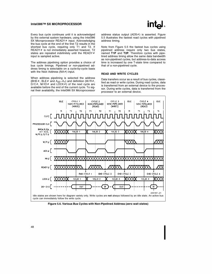
Intel386TM SX MICROPROCESSOR
Every bus cycle continues until it is acknowledgedby the external system hardware, using the Intel386SX Microprocessor READYÝ input. Acknowledgingthe bus cycle at the end of the first T2 results in theshortest bus cycle, requiring only T1 and T2. IfREADYÝ is not immediately asserted however, T2states are repeated indefinitely until the READYÝinput is sampled active.
The address pipelining option provides a choice ofbus cycle timings. Pipelined or non-pipelined ad-dress timing is selectable on a cycle-by-cycle basiswith the Next Address (NAÝ) input.
When address pipelining is selected the address(BHEÝ, BLEÝ and A23–A1) and definition (W/RÝ,D/CÝ, M/IOÝ and LOCKÝ) of the next cycle areavailable before the end of the current cycle. To sig-nal their availability, the Intel386 SX Microprocessor
address status output (ADSÝ) is asserted. Figure5.5 illustrates the fastest read cycles with pipelinedaddress timing.
Note from Figure 5.5 the fastest bus cycles usingpipelined address require only two bus states,named T1P and T2P. Therefore cycles with pipe-lined address timing allow the same data bandwidthas non-pipelined cycles, but address-to-data accesstime is increased by one T-state time compared tothat of a non-pipelined cycle.
READ AND WRITE CYCLES
Data transfers occur as a result of bus cycles, classi-fied as read or write cycles. During read cycles, datais transferred from an external device to the proces-sor. During write cycles, data is transferred from theprocessor to an external device.
240187–21
Idle states are shown here for diagram variety only. Write cycles are not always followed by an idle state. An active buscycle can immediately follow the write cycle.
Figure 5.6. Various Bus Cycles with Non-Pipelined Address (zero wait states)
48

Intel386TM SX MICROPROCESSOR
Two choices of address timing are dynamically se-lectable: non-pipelined or pipelined. After an idle busstate, the processor always uses non-pipelined ad-dress timing. However the NAÝ (Next Address) in-put may be asserted to select pipelined address tim-ing for the next bus cycle. When pipelining is select-ed and the Intel386 SX Microprocessor has a busrequest pending internally, the address and defini-tion of the next cycle is made available even beforethe current bus cycle is acknowledged by READYÝ.
Terminating a read or write cycle, like any bus cycle,requires acknowledging the cycle by asserting theREADYÝ input. Until acknowledged, the processorinserts wait states into the bus cycle, to allow adjust-ment for the speed of any external device. Externalhardware, which has decoded the address and buscycle type, asserts the READYÝ input at the appro-priate time.
At the end of the second bus state within the buscycle, READYÝ is sampled. At that time, if externalhardware acknowledges the bus cycle by assertingREADYÝ, the bus cycle terminates as shown in Fig-ure 5.6. If READYÝ is negated as in Figure 5.7, theIntel386 SX Microprocessor executes another busstate (a wait state) and READYÝ is sampled againat the end of that state. This continues indefinitelyuntil the cycle is acknowledged by READYÝ assert-ed.
When the current cycle is acknowledged, theIntel386 SX Microprocessor terminates it. When aread cycle is acknowledged, the Intel386 SX Micro-processor latches the information present at its datapins. When a write cycle is acknowledged, theIntel386 SX CPU’s write data remains valid through-out phase one of the next bus state, to provide writedata hold time.
240187–22
Idle states are shown here for diagram variety only. Write cycles are not always followed by an idle state. An active buscycle can immediately follow the write cycle.
Figure 5.7. Various Bus Cycles with Non-Pipelined Address (various number of wait states)
49

Intel386TM SX MICROPROCESSOR
Non-Pipelined Address
Any bus cycle may be performed with non-pipelinedaddress timing. For example, Figure 5.6 shows amixture of read and write cycles with non-pipelinedaddress timing. Figure 5.6 shows that the fastestpossible cycles with non-pipelined address have twobus states per bus cycle. The states are named T1and T2. In phase one of T1, the address signals andbus cycle definition signals are driven valid and, tosignal their availability, address strobe (ADSÝ) issimultaneously asserted.
During read or write cycles, the data bus behaves asfollows. If the cycle is a read, the Intel386 SX Micro-processor floats its data signals to allow driving bythe external device being addressed. The Intel386SX Microprocessor requires that all data buspins be at a valid logic state (HIGH or LOW) atthe end of each read cycle, when READYÝ isasserted. The system MUST be designed tomeet this requirement. If the cycle is a write, datasignals are driven by the Intel386 SX Microproces-sor beginning in phase two of T1 until phase one ofthe bus state following cycle acknowledgment.
Figure 5.7 illustrates non-pipelined bus cycles withone wait state added to Cycles 2 and 3. READYÝ issampled inactive at the end of the first T2 in Cycles2 and 3. Therefore Cycles 2 and 3 have T2 repeatedagain. At the end of the second T2, READYÝ issampled active.
When address pipelining is not used, the addressand bus cycle definition remain valid during all waitstates. When wait states are added and it is desir-able to maintain non-pipelined address timing, it isnecessary to negate NAÝ during each T2 state ex-cept the last one, as shown in Figure 5.7 Cycles 2and 3. If NAÝ is sampled active during a T2 otherthan the last one, the next state would be T2I or T2Pinstead of another T2.
When address pipelining is not used, the bus statesand transitions are completely illustrated by Figure5.8. The bus transitions between four possiblestates, T1, T2, Ti, and Th. Bus cycles consist of T1and T2, with T2 being repeated for wait states. Oth-erwise the bus may be idle, Ti, or in the hold ac-knowledge state Th.
240187–23
Bus States:T1Ðfirst clock of a non-pipelined bus cycle (Intel386TM SX CPU drives new address and asserts ADSÝ).T2Ðsubsequent clocks of a bus cycle when NAÝ has not been sampled asserted in the current bus cycle.TiÐidle state.ThÐhold acknowledge state (Intel386 SX CPU asserts HLDA).The fastest bus cycle consists of two states T1 and T2.Four basic bus states describe bus operation when not using pipelined address.
Figure 5.8. Bus States (not using pipelined address)
50

Intel386TM SX MICROPROCESSOR
Bus cycles always begin with T1. T1 always leads toT2. If a bus cycle is not acknowledged during T2 andNAÝ is inactive, T2 is repeated. When a cycle isacknowledged during T2, the following state will beT1 of the next bus cycle if a bus request is pendinginternally, or Ti if there is no bus request pending, orTh if the HOLD input is being asserted.
Use of pipelined address allows the Intel386 SX Mi-croprocessor to enter three additional bus states notshown in Figure 5.8. Figure 5.12 is the complete busstate diagram, including pipelined address cycles.
Pipelined Address
Address pipelining is the option of requesting theaddress and the bus cycle definition of the next in-
ternally pending bus cycle before the current buscycle is acknowledged with READYÝ asserted.ADSÝ is asserted by the Intel386 SX Microproces-sor when the next address is issued. The addresspipelining option is controlled on a cycle-by-cyclebasis with the NAÝ input signal.
Once a bus cycle is in progress and the current ad-dress has been valid for at least one entire busstate, the NAÝ input is sampled at the end of everyphase one until the bus cycle is acknowledged. Dur-ing non-pipelined bus cycles NAÝ is sampled at theend of phase one in every T2. An example is Cycle 2in Figure 5.9, during which NAÝ is sampled at theend of phase one of every T2 (it was asserted onceduring the first T2 and has no further effect duringthat bus cycle).
240187–24
Following any idle bus state (Ti), addresses are non-pipelined. Within non-pipelined bus cycles, NAÝ is only sampledduring wait states. Therefore, to begin address pipelining during a group of non-pipelined bus cycles requires a non-pipe-lined cycle with at least one wait state (Cycle 2 above).
Figure 5.9. Transitioning to Pipelined Address During Burst of Bus Cycles
51

Intel386TM SX MICROPROCESSOR
If NAÝ is sampled active, the Intel386 SX Micro-processor is free to drive the address and bus cycledefinition of the next bus cycle, and assert ADSÝ,as soon as it has a bus request internally pending. Itmay drive the next address as early as the next busstate, whether the current bus cycle is acknowl-edged at that time or not.
Regarding the details of address pipelining, theIntel386 SX Microprocessor has the following char-acteristics:
1. The next address may appear as early as the busstate after NAÝ was sampled active (see Figures5.9 or 5.10). In that case, state T2P is enteredimmediately. However, when there is not an inter-nal bus request already pending, the next addresswill not be available immediately after NAÝ is as-serted and T2I is entered instead of T2P (see Fig-
ure 5.11 Cycle 3). Provided the current bus cycleisn’t yet acknowledged by READYÝ asserted,T2P will be entered as soon as the Intel386 SXMicroprocessor does drive the next address. Ex-ternal hardware should therefore observe theADSÝ output as confirmation the next address isactually being driven on the bus.
2. Any address which is validated by a pulse on theADSÝ output will remain stable on the addresspins for at least two processor clock periods. TheIntel386 SX Microprocessor cannot produce anew address more frequently than every twoprocessor clock periods (see Figures 5.9, 5.10,and 5.11).
3. Only the address and bus cycle definition of thevery next bus cycle is available. The pipelining ca-pability cannot look further than one bus cycleahead (see Figure 5.11 Cycle 1).
240187–25
Following any bus state (Ti) the address is always non-pipelined and NAÝ is only sampled during wait states. To startaddress pipelining after an idle state requires a non-pipelined cycle with at least one wait state (cycle 1 above)The pipelined cycles (2, 3, 4 above) are shown with various numbers of wait states.
Figure 5.10. Fastest Transition to Pipelined Address Following Idle Bus State
52

Intel386TM SX MICROPROCESSOR
The complete bus state transition diagram, includingoperation with pipelined address is given by Figure5.12. Note it is a superset of the diagram for non-pipelined address only, and the three additional busstates for pipelined address are drawn in bold.
The fastest bus cycle with pipelined address con-sists of just two bus states, T1P and T2P (recall fornon-pipelined address it is T1 and T2). T1P is thefirst bus state of a pipelined cycle.
240187–26
Figure 5.11. Details of Address Pipelining During Cycles with Wait States
53

Intel386TM SX MICROPROCESSOR
Bus States:T1Ðfirst clock of a non-pipelined bus cycle (Intel386TM SX CPUdrives new address and asserts ADSÝ).T2Ðsubsequent clocks of a bus cycle when NAÝ has not beensampled asserted in the current bus cycle.T2IÐsubsequent clocks of a bus cycle when NAÝ has beensampled asserted in the current bus cycle but there is not yetan internal bus request pending (Intel386 SX CPU will not drivenew address or assert ADSÝ).T2PÐsubsequent clocks of a bus cycle when NAÝ has beensampled asserted in the current bus cycle and there is an inter-nal bus request pending (Intel386 SX CPU drives new addressand asserts ADSÝ).T1PÐfirst clock of a pipelined bus cycle.TiÐidle state. 240187–27ThÐhold acknowledge state (Intel386 SX CPU asserts HLDA).Asserting NAÝ for pipelined address gives access to threemore bus states: T2I, T2P and T1P.Using pipelined address, the fastest bus cycle consists of T1Pand T2P.
Figure 5.12. Complete Bus States (including pipelined address)
54

Intel386TM SX MICROPROCESSOR
Initiating and Maintaining Pipelined Address
Using the state diagram Figure 5.12, observe thetransitions from an idle state, Ti, to the beginning ofa pipelined bus cycle T1P. From an idle state, Ti, thefirst bus cycle must begin with T1, and is therefore anon-pipelined bus cycle. The next bus cycle will bepipelined, however, provided NAÝ is asserted andthe first bus cycle ends in a T2P state (the addressfor the next bus cycle is driven during T2P). The fast-est path from an idle state to a bus cycle with pipe-lined address is shown in bold below:
Ti, Ti, Ti, T1 - T2 - T2P, T1P - T2P,
idle non-pipelined pipelined
states cycle cycle
T1-T2-T2P are the states of the bus cycle that es-tablish address pipelining for the next bus cycle,which begins with T1P. The same is true after a bushold state, shown below:
Th, Th, Th, T1 - T2 - T2P, T1P - T2P,
hold acknowledge non-pipelined pipelined
states cycle cycle
The transition to pipelined address is shown func-tionally by Figure 5.10 Cycle 1. Note that Cycle 1 isused to transition into pipelined address timing forthe subsequent Cycles 2, 3 and 4, which are pipe-lined. The NAÝ input is asserted at the appropriatetime to select address pipelining for Cycles 2, 3 and4.
Once a bus cycle is in progress and the current ad-dress has been valid for one entire bus state, theNAÝ input is sampled at the end of every phase oneuntil the bus cycle is acknowledged. Sampling be-gins in T2 during Cycle 1 in Figure 5.10. Once NAÝis sampled active during the current cycle, theIntel386 SX Microprocessor is free to drive a newaddress and bus cycle definition on the bus as earlyas the next bus state. In Figure 5.10 Cycle 1 forexample, the next address is driven during stateT2P. Thus Cycle 1 makes the transition to pipelinedaddress timing, since it begins with T1 but ends withT2P. Because the address for Cycle 2 is availablebefore Cycle 2 begins, Cycle 2 is called a pipelined
bus cycle, and it begins with T1P. Cycle 2 begins assoon as READYÝ asserted terminates Cycle 1.
Examples of transition bus cycles are Figure 5.10Cycle 1 and Figure 5.9 Cycle 2. Figure 5.10 showstransition during the very first cycle after an idle busstate, which is the fastest possible transition into ad-dress pipelining. Figure 5.9 Cycle 2 shows a tran-sition cycle occurring during a burst of bus cycles. Inany case, a transition cycle is the same whenever itoccurs: it consists at least of T1, T2 (NAÝ is assert-ed at that time), and T2P (provided the Intel386 SXMicroprocessor has an internal bus request alreadypending, which it almost always has). T2P states arerepeated if wait states are added to the cycle.
Note that only three states (T1, T2 and T2P) arerequired in a bus cycle performing a transition fromnon-pipelined address into pipelined address timing,for example Figure 5.10 Cycle 1. Figure 5.10 Cycles2, 3 and 4 show that address pipelining can be main-tained with two-state bus cycles consisting only ofT1P and T2P.
Once a pipelined bus cycle is in progress, pipelinedtiming is maintained for the next cycle by assertingNAÝ and detecting that the Intel386 SX Microproc-essor enters T2P during the current bus cycle. Thecurrent bus cycle must end in state T2P for pipelin-ing to be maintained in the next cycle. T2P is identi-fied by the assertion of ADSÝ. Figures 5.9 and 5.10however, each show pipelining ending after Cycle 4because Cycle 4 ends in T2I. This indicates theIntel386 SX Microprocessor didn’t have an internalbus request prior to the acknowledgement of Cycle4. If a cycle ends with a T2 or T2I, the next cycle willnot be pipelined.
Realistically, address pipelining is almost alwaysmaintained as long as NAÝ is sampled asserted.This is so because in the absence of any other re-quest, a code prefetch request is always internallypending until the instruction decoder and code pre-fetch queue are completely full. Therefore, addresspipelining is maintained for long bursts of bus cycles,if the bus is available (i.e., HOLD inactive) and NAÝis sampled active in each of the bus cycles.
55

Intel386TM SX MICROPROCESSOR
INTERRUPT ACKNOWLEDGE (INTA) CYCLES
In response to an interrupt request on the INTR in-put when interrupts are enabled, the Intel386 SX Mi-croprocessor performs two interrupt acknowledgecycles. These bus cycles are similar to read cyclesin that bus definition signals define the type of busactivity taking place, and each cycle continues untilacknowledged by READYÝ sampled active.
The state of A2 distinguishes the first and secondinterrupt acknowledge cycles. The byte addressdriven during the first interrupt acknowledge cycle is4 (A23–A3, A1, BLEÝ LOW, A2 and BHEÝ HIGH).The byte address driven during the second interruptacknowledge cycle is 0 (A23–A1, BLEÝ LOW, andBHEÝ HIGH).
The LOCKÝ output is asserted from the beginningof the first interrupt acknowledge cycle until the endof the second interrupt acknowledge cycle. Four idlebus states, Ti, are inserted by the Intel386 SX Micro-processor between the two interrupt acknowledgecycles for compatibility with spec TRHRL of the8259A Interrupt Controller.
During both interrupt acknowledge cycles, D15–D0float. No data is read at the end of the first interruptacknowledge cycle. At the end of the second inter-rupt acknowledge cycle, the Intel386 SX Microproc-essor will read an external interrupt vector from D7–D0 of the data bus. The vector indicates the specificinterrupt number (from 0–255) requiring service.
240187–28
Interrupt Vector (0–255) is read on D0–D7 at end of second interrupt Acknowledge bus cycle.Because each Interrupt Acknowledge bus cycle is followed by idle bus states. asserting NAÝ has no practical effect.Choose the approach which is simplest for your system hardware design.
Figure 5.13. Interrupt Acknowledge Cycles
56
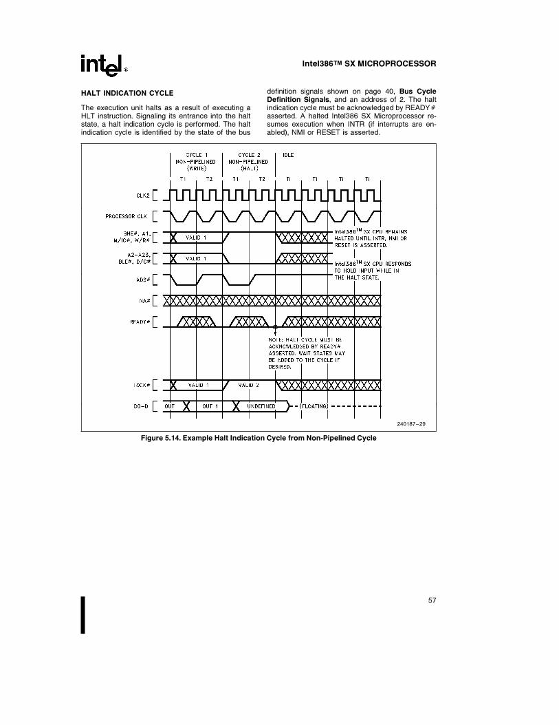
Intel386TM SX MICROPROCESSOR
HALT INDICATION CYCLE
The execution unit halts as a result of executing aHLT instruction. Signaling its entrance into the haltstate, a halt indication cycle is performed. The haltindication cycle is identified by the state of the bus
definition signals shown on page 40, Bus CycleDefinition Signals, and an address of 2. The haltindication cycle must be acknowledged by READYÝasserted. A halted Intel386 SX Microprocessor re-sumes execution when INTR (if interrupts are en-abled), NMI or RESET is asserted.
240187–29
Figure 5.14. Example Halt Indication Cycle from Non-Pipelined Cycle
57

Intel386TM SX MICROPROCESSOR
SHUTDOWN INDICATION CYCLE
The Intel386 SX Microprocessor shuts down as aresult of a protection fault while attempting to pro-cess a double fault. Signaling its entrance into theshutdown state, a shutdown indication cycle is per-formed. The shutdown indication cycle is identifiedby the state of the bus definition signals shown inBus Cycle Definition Signals and an address of 0.The shutdown indication cycle must be acknowl-edged by READYÝ asserted. A shutdown Intel386SX Microprocessor resumes execution when NMI orRESET is asserted.
ENTERING AND EXITING HOLDACKNOWLEDGE
The bus hold acknowledge state, Th, is entered inresponse to the HOLD input being asserted. In thebus hold acknowledge state, the Intel386 SX Micro-processor floats all outputs or bidirectional signals,except for HLDA. HLDA is asserted as long as theIntel386 SX Microprocessor remains in the bus holdacknowledge state. In the bus hold acknowledgestate, all inputs except HOLD, FLTÝ and RESET areignored.
240187–30
Figure 5.15. Example Shutdown Indication Cycle from Non-Pipelined Cycle
58

Intel386TM SX MICROPROCESSOR
Th may be entered from a bus idle state as in Figure5.16 or after the acknowledgement of the currentphysical bus cycle if the LOCKÝ signal is not assert-ed, as in Figures 5.17 and 5.18.
Th is exited in response to the HOLD input beingnegated. The following state will be Ti as in Figure5.16 if no bus request is pending. The following busstate will be T1 if a bus request is internally pending,as in Figures 5.17 and 5.18. Th is exited in responseto RESET being asserted.
If a rising edge occurs on the edge-triggered NMIinput while in Th, the event is remembered as a non-maskable interrupt 2 and is serviced when Th is exit-ed unless the Intel386 SX Microprocessor is resetbefore Th is exited.
RESET DURING HOLD ACKNOWLEDGE
RESET being asserted takes priority over HOLD be-ing asserted. If RESET is asserted while HOLD re-mains asserted, the Intel386 SX Microprocessordrives its pins to defined states during reset, as inTable 5.5 Pin State During Reset, and performsinternal reset activity as usual.
If HOLD remains asserted when RESET is inactive,the Intel386 SX Microprocessor enters the hold ac-knowledge state before performing its first bus cy-cle, provided HOLD is still asserted when theIntel386 SX Microprocessor would otherwise per-form its first bus cycle.
240187–31
NOTE:For maximum design flexibility the Intel386TM SX CPU has no internal pullup resistors on its outputs. Your design mayrequire an external pullup on ADSÝ and other outputs to keep them negated during float periods.
Figure 5.16. Requesting Hold from Idle Bus
59

Intel386TM SX MICROPROCESSOR
FLOAT
Activating the FLTÝ input floats all Intel386 SX bidi-rectional and output signals, including HLDA. Assert-ing FLTÝ isolates the Intel386 SX from the sur-rounding circuitry.
As the Intel386 SX is packaged in a surface mountPQFP, it cannot be removed from the motherboardwhen In-Circuit Emulation (ICE) is needed. TheFLTÝ input allows the Intel386 SX to be electricallyisolated from the surrounding circuitry. This allowsconnection of an emulator to the Intel386 SX PQFPwithout removing it from the PCB. This method ofemulation is referred to as ON-Circuit Emulation(ONCE).
ENTERING AND EXITING FLOAT
FLTÝ is an asynchronous, active-low input. It is rec-ognized on the rising edge of CLK2. When recog-nized, it aborts the current bus cycle and floats theoutputs of the Intel386 SX (Figure 5.20). FLTÝ mustbe held low for a minimum of 16 CLK2 cycles. Resetshould be asserted and held asserted until afterFLTÝ is deasserted. This will ensure that theIntel386 SX will exit float in a valid state.
Asserting the FLTÝ input unconditionally aborts thecurrent bus cycle and forces the Intel386 SX into theFLOAT mode. Since activating FLTÝ unconditional-ly forces the Intel386 SX into FLOAT mode, theIntel386 SX is not guaranteed to enter FLOAT in avalid state. After deactivating FLTÝ, the Intel386 SXis not guaranteed to exit FLOAT mode in a validstate. This is not a problem as the FLTÝ pin ismeant to be used only during ONCE. After exitingFLOAT, the Intel386 SX must be reset to return it toa valid state. Reset should be asserted before FLTÝis deasserted. This will ensure that the Intel386 SXwill exit float in a valid state.
FLTÝ has an internal pull-up resistor, and if it is notused it should be unconnected.
BUS ACTIVITY DURING AND FOLLOWINGRESET
RESET is the highest priority input signal, capable ofinterrupting any processor activity when it is assert-ed. A bus cycle in progress can be aborted at anystage, or idle states or bus hold acknowledge statesdiscontinued so that the reset state is established.
240187–32
NOTE:HOLD is a synchronous input and can be asserted at any CLK2 edge, provided setup and hold (t23 and t24) require-ments are met. This waveform is useful for determining Hold Acknowledge latency.
Figure 5.17. Requesting Hold from Active Bus (NAÝ inactive)
60

Intel386TM SX MICROPROCESSOR
RESET should remain asserted for at least 15 CLK2periods to ensure it is recognized throughout theIntel386 SX Microprocessor, and at least 80 CLK2periods if self-test is going to be requested at thefalling edge. RESET asserted pulses less than 15CLK2 periods may not be recognized. RESET puls-es less than 80 CLK2 periods followed by a self-testmay cause the self-test to report a failure when notrue failure exists.
Provided the RESET falling edge meets setup andhold times t25 and t26, the internal processor clockphase is defined at that time as illustrated by Figure5.19 and Figure 7.7.
A self-test may be requested at the time RESETgoes inactive by having the BUSYÝ input at a LOWlevel as shown in Figure 5.19. The self-test requiresapproximately (220 a 60) CLK2 periods to com-plete. The self-test duration is not affected by thetest results. Even if the self-test indicates a problem,the Intel386 SX Microprocessor attempts to proceedwith the reset sequence afterwards.
After the RESET falling edge (and after the self-testif it was requested) the Intel386 SX Microprocessorperforms an internal initialization sequence for ap-proximately 350 to 450 CLK2 periods.
240187–33
NOTE:HOLD is a synchronous input and can be asserted at any CLK2 edge, provided setup and hold (t23 and t24) require-ments are met. This waveform is useful for determining Hold Acknowledge latency.
Figure 5.18. Requesting Hold from Idle Bus (NAÝ active)
61

Intel386TM SX MICROPROCESSOR
240187–34
NOTES:1. BUSYÝ should be held stable for 8 CLK2 periods before and after the CLK2 period in which RESET falling edgeoccurs.2. If self-test is requested the outputs remain in their reset state as shown here.
Figure 5.19. Bus Activity from Reset Until First Code Fetch
240187–51
Figure 5.20. Entering and Exiting, FLTÝ
62

Intel386TM SX MICROPROCESSOR
5.5 Self-test Signature
Upon completion of self-test (if self-test was re-quested by driving BUSYÝ LOW at the falling edgeof RESET) the EAX register will contain a signatureof 00000000H indicating the Intel386 SX Microproc-essor passed its self-test of microcode and majorPLA contents with no problems detected. The pass-ing signature in EAX, 00000000H, applies to all revi-sion levels. Any non-zero signature indicates the unitis faulty.
5.6 Component and RevisionIdentifiers
To assist users, the Intel386 SX Microprocessor af-ter reset holds a component identifier and revisionidentifier in its DX register. The upper 8 bits of DXhold 23H as identification of the Intel386 SX Micro-processor (the lower nibble, 03H, refers to theIntel386 DX Architecture. The upper nibble, 02H, re-fers to the second member of the Intel386 DX Fami-ly). The lower 8 bits of DX hold an 8-bit unsignedbinary number related to the component revisionlevel. The revision identifier will, in general, chrono-logically track those component steppings which areintended to have certain improvements or distinctionfrom previous steppings. The Intel386 SX Microproc-essor revision identifier will track that of the Intel386DX CPU where possible.
The revision identifier is intended to assist users to apractical extent. However, the revision identifier val-ue is not guaranteed to change with every steppingrevision, or to follow a completely uniform numericalsequence, depending on the type or intention of re-vision, or manufacturing materials required to bechanged. Intel has sole discretion over these char-acteristics of the component.
Table 5.7. Component and
Revision Identifier History
Stepping Revision Identifier
A0 04H
B 05H
C 08H
D 08H
E 08H
5.7 Coprocessor Interfacing
The Intel386 SX Microprocessor provides an auto-matic interface for the Intel Intel387 SX numericfloating-point coprocessor. The Intel387 SX coproc-essor uses an I/O mapped interface driven automat-ically by the Intel386 SX Microprocessor and assist-ed by three dedicated signals: BUSYÝ, ERRORÝand PEREQ.
As the Intel386 SX Microprocessor begins support-ing a coprocessor instruction, it tests the BUSYÝand ERRORÝ signals to determine if the coproces-
sor can accept its next instruction. Thus, theBUSYÝ and ERRORÝ inputs eliminate the need forany ‘preamble’ bus cycles for communication be-tween processor and coprocessor. The Intel387 SXcan be given its command opcode immediately. Thededicated signals provide instruction synchroniza-tion, and eliminate the need of using the WAIT op-code (9BH) for Intel387 SX instruction synchroniza-tion (the WAIT opcode was required when the 8086or 8088 was used with the 8087 coprocessor).
Custom coprocessors can be included in Intel386SX Microprocessor based systems by memory-mapped or I/O-mapped interfaces. Such coproces-sor interfaces allow a completely custom protocol,and are not limited to a set of coprocessor protocol‘primitives’. Instead, memory-mapped or I/O-mapped interfaces may use all applicable instruc-tions for high-speed coprocessor communication.The BUSYÝ and ERRORÝ inputs of the Intel386SX Microprocessor may also be used for the customcoprocessor interface, if such hardware assist is de-sired. These signals can be tested by the WAIT op-code (9BH). The WAIT instruction will wait until theBUSYÝ input is inactive (interruptable by an NMI orenabled INTR input), but generates an exception 16fault if the ERRORÝ pin is active when the BUSYÝgoes (or is) inactive. If the custom coprocessor inter-face is memory-mapped, protection of the address-es used for the interface can be provided with theIntel386 SX CPU’s on-chip paging or segmentationmechanisms. If the custom interface is I/O-mapped,protection of the interface can be provided with theIOPL (I/O Privilege Level) mechanism.
The Intel387 SX numeric coprocessor interface isI/O mapped as shown in Table 5.8. Note that theIntel387 SX coprocessor interface addresses arebeyond the 0H-0FFFFH range for programmed I/O.When the Intel386 SX Microprocessor supports theIntel387 SX coprocessor, the Intel386 SX Micro-processor automatically generates bus cycles to thecoprocessor interface addresses.
Table 5.8. Numeric Coprocessor Port Addresses
Address in Intel386 SX Intel387 SX
CPU I/O Space Coprocessor Register
8000F8H Opcode Register
8000FCH/8000FEH* Operand Register
*Generated as 2nd bus cycle during Dword transfer.
To correctly map the Intel387 SX registers to theappropriate I/O addresses, connect the CMD0 andCMD1 lines of the Intel387 SX as listed in Table 5.9.
Table 5.9. Connections for CMD0
and CMD1 Inputs for the Intel387 SX
Signal Connection
CMD0 Connect directly
to Intel386 SX CPU A2 signal
CMD1 Connect to ground.
63

Intel386TM SX MICROPROCESSOR
Software Testing for Coprocessor Presence
When software is used to test for coprocessor(Intel387 SX) presence, it should use only the follow-ing coprocessor opcodes: FINIT, FNINIT, FSTCWmem, FSTSW mem and FSTSW AX. To use othercoprocessor opcodes when a coprocessor is knownto be not present, first set EM e 1 in the Intel386 SXCPU’s CR0 register.
6.0 PACKAGE THERMALSPECIFICATIONS
The Intel386 SX Microprocessor is specified for op-eration when case temperature (Tc) is within therange of 0§C–100§C. The case temperature may bemeasured in any environment, to determine whetherthe Intel386 SX Microprocessor is within specifiedoperating range. The case temperature should bemeasured at the center of the top surface oppositethe pins.
The ambient temperature (Ta) is related to Tc andthe thermal conductivity parameters ija and ijc fromthe following equations (eqn. 3 is derived by elimi-nating the junction temperature (Tj) between eqns.1 and 2):
1) Tj e Tc a P*ijc
2) Ta e Tj b P*ija
3) Tc e Ta a P*[ija b ijc]
Values for ija and ijc are given in Table 6.1 for the100 lead fine pitch. ija is given at various airflows.The power (P) dissipated by the chip as heat isVcc*Icc. A guaranteed maximum safe Ta can be cal-culated from eqn. 3 by using the maximum safe Tc of100§C, along with the maximum power drawn by thechip in the given design, and ijc and ija values fromTable 6.1. (The ija value depends on the airflow,measured at the top of the chip, provided by thesystem ventilation.)
7.0 ELECTRICAL SPECIFICATIONS
The following sections describe recommended elec-trical connections for the Intel386 SX Microproces-sor, and its electrical specifications.
7.1 Power and Grounding
The Intel386 SX Microprocessor is implemented inCHMOS IV technology and has modest power re-quirements. However, its high clock frequency and47 output buffers (address, data, control, and HLDA)can cause power surges as multiple output buffersdrive new signal levels simultaneously. For clean on-chip power distribution at high frequency, 14 Vccand 18 Vss pins separately feed functional units ofthe Intel386 SX Microprocessor.
Power and ground connections must be made to allexternal Vcc and Vss pins of the Intel386 SX Micro-processor. On the circuit board, all Vcc pins shouldbe connected on a Vcc plane and all Vss pinsshould be connected on a GND plane.
POWER DECOUPLING RECOMMENDATIONS
Liberal decoupling capacitors should be placed nearthe Intel386 SX Microprocessor. The Intel386 SX Mi-croprocessor driving its 24-bit address bus and16-bit data bus at high frequencies can cause tran-sient power surges, particularly when driving largecapacitive loads. Low inductance capacitors and in-terconnects are recommended for best high fre-quency electrical performance. Inductance can bereduced by shortening circuit board traces betweenthe Intel386 SX Microprocessor and decoupling ca-pacitors as much as possible.
Table 6.1. Thermal Resistances (§C/Watt) ijc and ija.
ija versus Airflow - ft/min (m/sec)
Package ijc 0 200 400 600 800 1000
(0) (1.01) (2.03) (3.04) (4.06) (5.07)
100 Lead7.5 34.5 29.5 25.5 22.5 21.5 21
Fine Pitch
64

Intel386TM SX MICROPROCESSOR
Table 7.1. Recommended Resistor Pull-ups to Vcc
Pin Signal Pull-up Value Purpose
16 ADSÝ 20 KX g10% Lightly pull ADSÝ inactive duringIntel386TM SX CPU hold acknowledgestates
26 LOCKÝ 20 KX g10% Lightly pull LOCKÝ inactive duringIntel386TM SX CPU hold acknowledgestates
RESISTOR RECOMMENDATIONS
The ERRORÝ, FLTÝ and BUSYÝ inputs have inter-nal pull-up resistors of approximately 20 KX and thePEREQ input has an internal pull-down resistor ofapproximately 20 KX built into the Intel386 SX Mi-croprocessor to keep these signals inactive whenthe Intel387 SX is not present in the system (or tem-porarily removed from its socket).
In typical designs, the external pull-up resistorsshown in Table 7.1 are recommended. However, aparticular design may have reason to adjust the re-sistor values recommended here, or alter the use ofpull-up resistors in other ways.
OTHER CONNECTION RECOMMENDATIONS
For reliable operation, always connect unused in-puts to an appropriate signal level. N/C pins shouldalways remain unconnected. Connection of N/Cpins to Vcc or Vss will result in component mal-function or incompatibility with future steppingsof the Intel386 SX Microprocessor.
Particularly when not using interrupts or bus hold (aswhen first prototyping), prevent any chance of spuri-ous activity by connecting these associated inputs toGND:
Pin Signal
40 INTR
38 NMI
4 HOLD
If not using address pipelining, connect pin 6, NAÝ,through a pull-up in the range of 20 KX to Vcc.
7.2 Maximum Ratings
Table 7.2. Maximum Ratings
Parameter Maximum Rating
Storage temperature b65 §C to 150 §CCase temperature under bias b65 §C to 110 §CSupply voltage with respect
to Vss b.5V to 6.5V
Voltage on other pins b.5V to (Vcca.5)V
Table 7.2 gives stress ratings only, and functionaloperation at the maximums is not guaranteed. Func-tional operating conditions are given in section 7.3,D.C. Specifications, and section 7.4, A.C. Specifi-cations.
Extended exposure to the Maximum Ratings may af-fect device reliability. Furthermore, although theIntel386 SX Microprocessor contains protective cir-cuitry to resist damage from static electric discharge,always take precautions to avoid high static voltagesor electric fields.
65

Intel386TM SX MICROPROCESSOR
7.3 D.C. SpecificationsFunctional operating range: VCC e 5V g10%; TCASE e 0§C to 100§C
Table 7.3. Intel386TM SX Microprocessor D.C. CharacteristicsÐ33 MHz, 25 MHz, 20 MHz and 16 MHz
Symbol Parameter Min Max Unit Test Condition
VIL Input LOW Voltage b0.3 a0.8 V
VIH Input HIGH Voltage 2.0 VCCa0.3 V
VILC CLK2 Input LOW Voltage b0.3 a0.8 V
VIHC CLK2 Input HIGH Voltage VCCb0.8 VCCa0.3 V
VOL Output LOW Voltage
IOLe4 mA: A23–A1,D15–D0 0.45 V
IOLe5 mA: BHEÝ,BLEÝ,W/RÝ,D/CÝ, 0.45 V
M/IOÝ,LOCKÝ,ADSÝ,HLDA
VOH Output HIGH Voltage
IOHeb1 mA: A23–A1,D15–D0 2.4 V
IOHeb0.2 mA: A23–A1,D15–D0 VCCb0.5 V
IOHeb0.9 mA: BHEÝ,BLEÝ,W/RÝ, 2.4 V
D/CÝ,M/IOÝ,LOCKÝ,
ADSÝ,HLDA
IOHeb0.18 mA: BHEÝ,BLEÝ,W/RÝ, VCCb0.5 V
D/CÝ,M/IOÝ,LOCKÝ,
ADSÝ,HLDA
ILI Input Leakage Current g15 mA 0VsVINsVCC
(for all pins except PEREQ, BUSYÝ, FLTÝand ERRORÝ)
IIH Input Leakage Current 200 mA VIHe2.4V, Note 1
(PEREQ pin)
IIL Input Leakage Current b400 mA VILe0.45V, Note 2
(BUSYÝ, ERRORÝ and FLTÝ pins)
ILO Output Leakage Current g15 mA 0.45VsVOUTsVCC
ICC Supply Current (See Note 3)
CLK2e32 MHz: with 16 MHz Intel386 SX CPU 220 mA ICC type150 mA
CLK2e40 MHz: with 20 MHz Intel386 SX CPU 250 mA ICC type180 mA
CLK2e50 MHz: with 25 MHz Intel386 SX CPU 280 mA ICC type210 mA
CLK2e66 MHz: with 33 MHz Intel386 SX CPU 380 mA ICC type290 mA
CIN Input Capacitance 10 pF FCe1 MHz, Note 4
COUT Output or I/O Capacitance 12 pF FCe1 MHz, Note 4
CCLK CLK2 Capacitance 20 pF FCe1 MHz, Note 4
All values except ICC tested at the minimum operating frequency of the part (CLK2 e 8 MHz).
NOTES:1. PEREQ input has an internal pull-down resistor.2. BUSYÝ, FLTÝ and ERRORÝ inputs each have an internal pull-up resistor.3. ICC max measurement at worst case frequency, VCC and temperature, with 50 pF output load.4. Not 100% tested.
66

Intel386TM SX MICROPROCESSOR
Functional operating range: VCC e 5V g10%; TCASE e 0§C to 100§C
Table 7.4. Low Power (LP) Intel386TM SX Microprocessor
D.C. CharacteristicsÐ33 MHz, 25 MHz, 20 MHz, 16 MHz, and 12 MHz
Symbol Parameter Min Max Unit Test Condition
VIL Input LOW Voltage b0.3 a0.8 V
VIH Input HIGH Voltage 2.0 VCCa0.3 V
VILC CLK2 Input LOW Voltage b0.3 a0.8 V
VIHC CLK2 Input HIGH Voltage VCCb0.8 VCCa0.3 V
VOL Output LOW Voltage
IOLe4 mA: A23–A1,D15–D0 0.45 V
IOLe5 mA: BHEÝ,BLEÝ,W/RÝ,D/CÝ, 0.45 V
M/IOÝ,LOCKÝ,ADSÝ,HLDA
VOH Output HIGH Voltage
IOHeb1 mA: A23–A1,D15–D0 2.4 V
IOHeb0.2 mA: A23–A1,D15–D0 VCCb0.5 V
IOHeb0.9 mA: BHEÝ,BLEÝ,W/RÝ, 2.4 V
D/CÝ,M/IOÝ,LOCKÝ,
ADSÝ,HLDA
IOHeb0.18 mA: BHEÝ,BLEÝ,W/RÝ, VCCb0.5 V
D/CÝ,M/IOÝ,LOCKÝ,
ADSÝ,HLDA
ILI Input Leakage Current g15 mA 0VsVINsVCC
(for all pins except PEREQ, BUSYÝ, FLTÝand ERRORÝ)
IIH Input Leakage Current 200 mA VIHe2.4V, Note 1
(PEREQ pin)
IIL Input Leakage Current b400 mA VILe0.45V, Note 2
(BUSYÝ, ERRORÝ and FLTÝ pins)
ILO Output Leakage Current g15 mA 0.45VsVOUTsVCC
ICC Supply Current (See Note 3)
CLK2e4 MHz 100 mA ICC type50 mA
CLK2e24 MHz: with 12 MHz Intel386 SX CPU 190 mA ICC type120 mA
CLK2e32 MHz: with 16 MHz Intel386 SX CPU 220 mA ICC type150 mA
CLK2e40 MHz: with 20 MHz Intel386 SX CPU 250 mA ICC type180 mA
CLK2e50 MHz: with 25 MHz Intel386 SX CPU 280 mA ICC type210 mA
CLK2e66 MHz: with 33 MHz Intel386 SX CPU 380 mA ICC type290 mA
CIN Input Capacitance 10 pF FCe1 MHz, Note 4
COUT Output or I/O Capacitance 12 pF FCe1 MHz, Note 4
CCLK CLK2 Capacitance 20 pF FCe1 MHz, Note 4
All values except ICC tested at the minimum operating frequency of the part (CLK2 e 4 MHz).
NOTES:1. PEREQ input has an internal pull-down resistor.2. BUSYÝ, FLTÝ and ERRORÝ inputs each have an internal pull-up resistor.3. ICC max measurement at worst case frequency, VCC and temperature, with 50 pF output load.4. Not 100% tested.
67

Intel386TM SX MICROPROCESSOR
7.4 A.C. Specifications
The A.C. specifications given in Tables 7.5 through7.8 consist of output delays, input setup require-ments and input hold requirements. All A.C. specifi-cations are relative to the CLK2 rising edge crossingthe 2.0V level.
A.C. spec measurement is defined by Figure 7.1. In-puts must be driven to the voltage levels indicatedby Figure 7.1 when A.C. specifications are mea-sured. Output delays are specified with minimumand maximum limits measured as shown. The mini-mum delay times are hold times provided to externalcircuitry. Input setup and hold times are specified
as minimums, defining the smallest acceptable sam-pling window. Within the sampling window, a syn-chronous input signal must be stable for correct op-eration.
Outputs ADSÝ, W/RÝ, D/CÝ, M/IOÝ, LOCKÝ,BHEÝ, BLEÝ, A23–A1 and HLDA only change atthe beginning of phase one. D15–D0 (write cycles)only change at the beginning of phase two. TheREADYÝ, HOLD, BUSYÝ, ERRORÝ, PEREQ,FLTÝ and D15–D0 (read cycles) inputs are sampledat the beginning of phase one. The NAÝ, INTR andNMI inputs are sampled at the beginning of phasetwo.
240187–35
LEGENDA Ð Maximum Output Delay SpecB Ð Minimum Output Delay SpecC Ð Minimum Input Setup SpecD Ð Minimum Input Hold Spec
Figure 7.1. Drive Levels and Measurement Points for A.C. Specifications
68

Intel386TM SX MICROPROCESSOR
A.C. SPECIFICATIONS
Functional operating range: VCC e 5V g10%; TCASE e 0§C to 100§C
Table 7.5. Intel386TM SX Microprocessor A.C. CharacteristicsÐ33 MHz and 25 MHz
Symbol Parameter
33 MHz 25 MHz
Unit Figure NotesIntel386 SX Intel386 SX
Min Max Min Max
Operating Frequency 4 33 4 25 MHz Half CLK2 Frequency
t1 CLK2 Period 15 125 20 125 ns 7.3
t2a CLK2 HIGH Time 6.25 7 ns 7.3 at 2V(3)
t2b CLK2 HIGH Time 4.0 4 ns 7.3 at (VCCb0.8)V(3); Note 3
t3a CLK2 LOW Time 6.25 7 ns 7.3 at 2V(3)
t3b CLK2 LOW Time 4.5 5 ns 7.3 at 0.8V(3)
t4 CLK2 Fall Time 4 7 ns 7.3 (VCCb0.8)V to 0.8V(3)
t5 CLK2 Rise Time 4 7 ns 7.3 0.8V to (VCCb0.8)V(3)
t6 A23–A1 Valid Delay 4 15 4 17 ns 7.5 CL e 50 pF(4)
t7 A23–A1 Float Delay 4 20 4 30 ns 7.6 (Note 1)
t8 BHEÝ, BLEÝ, LOCKÝ 4 15 4 17 ns 7.5 CL e 50 pF(4)
Valid Delay
t9 BHEÝ, BLEÝ, LOCKÝ 4 20 4 30 ns 7.6 (Note 1)
Float Delay
t10 W/RÝ, M/IOÝ, D/CÝ, 4 15 4 17 ns 7.5 CL e 50 pF(4)
ADSÝ Valid Delay
t11 W/RÝ, M/IOÝ, D/CÝ, 4 20 4 30 ns 7.6 (Note 1)
ADSÝ Float Delay
t12 D15–D0 Write Data 7 23 7 23 ns 7.5 CL e 50 pF(4, 5)
Valid Delay
t12a D15–D0 Write Data 2 2 ns CL e 50 pF(4)
Hold Time
t13 D15–D0 Write Data 4 17 4 22 ns 7.6 (Note 1)
Float Delay
t14 HLDA Valid Delay 4 20 4 22 ns 7.6 CL e 75 pF(4)
t15 NAÝ Setup Time 5 5 ns 7.4
t16 NAÝ Hold Time 2 3 ns 7.4
t19 READYÝ Setup Time 7 9 ns 7.4
t20 READYÝ Hold Time 4 4 ns 7.4
t21 D15–D0 Read Data 5 7 ns 7.4
Setup Time
t22 D15–D0 Read Data 3 5 ns 7.4
Hold Time
69

Intel386TM SX MICROPROCESSOR
Functional operating range: VCC e 5V g10%; TCASE e 0§C to 100§C
Table 7.5. Intel386TM SX Microprocessor A.C. CharacteristicsÐ33 MHz and 25 MHz (Continued)
Symbol Parameter
33 MHz 25 MHz
Unit Figure NotesIntel386 SX Intel386 SX
Min Max Min Max
t23 HOLD Setup Time 9 9 ns 7.4
t24 HOLD Hold Time 2 3 ns 7.4
t25 RESET Setup Time 5 8 ns 7.7
t26 RESET Hold Time 2 3 ns 7.7
t27 NMI, INTR Setup Time 5 6 ns 7.4 (Note 2)
t28 NMI, INTR Hold Time 5 6 ns 7.4 (Note 2)
t29 PEREQ, ERRORÝ, BUSYÝ, 5 6 ns 7.4 (Note 2)
FLTÝ Setup Time
t30 PEREQ, ERRORÝ, BUSYÝ, 4 5 ns 7.4 (Note 2)
FLTÝ Hold Time
NOTES:1. Float condition occurs when maximum output current becomes less than ILO in magnitude. Float delay is not 100%tested.2. These inputs are allowed to be asynchronous to CLK2. The setup and hold specifications are given for testing purposesto assure recognition within a specific CLK2 period.3. These are not tested. They are guaranteed by design characterization.4. Tested with CL set at 50 pF. See Figures 7 and 8 for load capacitance derating curve.5. Minimum time not 100% tested.
Table 7.6. Low Power (LP) Intel386TM SX Microprocessor A.C. CharacteristicsÐ33 MHz and 25 MHz
Symbol Parameter
33 MHz 25 MHz
Unit Figure NotesIntel386 SX Intel386 SX
Min Max Min Max
Operating Frequency 2 33 2 25 MHz Half CLK2 Frequency
t1 CLK2 Period 15 250 20 250 ns 7.3
t2a CLK2 HIGH Time 6.25 7 ns 7.3 at 2V(3)
t2b CLK2 HIGH Time 4.0 4 ns 7.3 at (VCCb0.8)V(3); Note 3
t3a CLK2 LOW Time 6.25 7 ns 7.3 at 2V(3)
t3b CLK2 LOW Time 4.5 5 ns 7.3 at 0.8V(3)
t4 CLK2 Fall Time 4 7 ns 7.3 (VCCb0.8)V to 0.8V(3)
t5 CLK2 Rise Time 4 7 ns 7.3 0.8V to (VCCb0.8)V(3)
t6 A23–A1 Valid Delay 4 15 4 17 ns 7.5 CL e 50 pF(4)
t7 A23–A1 Float Delay 4 20 4 30 ns 7.6 (Note 1)
t8 BHEÝ, BLEÝ, LOCKÝ 4 15 4 17 ns 7.5 CL e 50 pF(4)
Valid Delay
t9 BHEÝ, BLEÝ, LOCKÝ 4 20 4 30 ns 7.6 (Note 1)
Float Delay
70

Intel386TM SX MICROPROCESSOR
Functional operating range: VCC e 5V g10%; TCASE e 0§C to 100§C
Table 7.6. Low Power (LP) Intel386TM SX Microprocessor
A.C. CharacteristicsÐ33 MHz and 25 MHz (Continued)
Symbol Parameter
33 MHz 25 MHz
Unit Figure NotesIntel386 SX Intel386 SX
Min Max Min Max
t10 W/RÝ, M/IOÝ, D/CÝ, 4 15 4 17 ns 7.5 CL e 50 pF(4)
ADSÝ Valid Delay
t11 W/RÝ, M/IOÝ, D/CÝ, 4 20 4 30 ns 7.6 (Note 1)
ADSÝ Float Delay
t12 D15–D0 Write Data 7 23 7 23 ns 7.5 CL e 50 pF(4, 5)
Valid Delay
t12a D15–D0 Write Data 2 2 ns CL e 50 pF(4)
Hold Time
t13 D15–D0 Write Data 4 17 4 22 ns 7.6 (Note 1)
Float Delay
t14 HLDA Valid Delay 4 20 4 22 ns 7.6 CL e 50 pF(4)
t15 NAÝ Setup Time 5 5 ns 7.4
t16 NAÝ Hold Time 2 3 ns 7.4
t19 READYÝ Setup Time 7 9 ns 7.4
t20 READYÝ Hold Time 4 4 ns 7.4
t21 D15–D0 Read Data 5 7 ns 7.4
Setup Time
t22 D15–D0 Read Data 3 5 ns 7.4
Hold Time
t23 HOLD Setup Time 9 9 ns 7.4
t24 HOLD Hold Time 2 3 ns 7.4
t25 RESET Setup Time 5 8 ns 7.7
t26 RESET Hold Time 2 3 ns 7.7
t27 NMI, INTR Setup Time 5 6 ns 7.4 (Note 2)
t28 NMI, INTR Hold Time 5 6 ns 7.4 (Note 2)
t29 PEREQ, ERRORÝ, BUSYÝ, 5 6 ns 7.4 (Note 2)
FLTÝ Setup Time
t30 PEREQ, ERRORÝ, BUSYÝ, 4 5 ns 7.4 (Note 2)
FLTÝ Hold Time
NOTES:1. Float condition occurs when maximum output current becomes less than ILO in magnitude. Float delay is not 100%tested.2. These inputs are allowed to be asynchronous to CLK2. The setup and hold specifications are given for testing purposesto assure recognition within a specific CLK2 period.3. These are not tested. They are guaranteed by design characterization.4. Tested with CL set at 50 pF. See Figures 7 and 8 for load capacitance derating curve.5. Minimum time not 100% tested.
71

Intel386TM SX MICROPROCESSOR
Functional operating range: VCC e 5V g10%; TCASE e 0§C to 100§C
Table 7.7. Intel386TM SX A.C. CharacteristicsÐ20 MHz and 16 MHz
Symbol Parameter
20 MHz 16 MHz
Unit Figure NotesIntel386 SX Intel386 SX
Min Max Min Max
Operating Frequency 4 20 4 16 MHz Half CLK2 Frequency
t1 CLK2 Period 25 125 31 125 ns 7.3
t2a CLK2 HIGH Time 8 9 ns 7.3 at 2V(3)
t2b CLK2 HIGH Time 5 5 ns 7.3 at (VCCb0.8)V(3)
t3a CLK2 LOW Time 8 9 ns 7.3 at 2V(3)
t3b CLK2 LOW Time 6 7 ns 7.3 at 0.8V(3)
t4 CLK2 Fall Time 8 8 ns 7.3 (VCCb0.8)V to 0.8V(3)
t5 CLK2 Rise Time 8 8 ns 7.3 0.8V to (VCCb0.8)V(3)
t6 A23–A1 Valid Delay 4 30 4 36 ns 7.5 CL e 120 pF(4)
t7 A23–A1 Float Delay 4 32 4 40 ns 7.6 (Note 1)
t8 BHEÝ, BLEÝ, LOCKÝ 4 30 4 36 ns 7.5 CL e 75 pF(4)
Valid Delay
t9 BHEÝ, BLEÝ, LOCKÝ 4 32 4 40 ns 7.6 (Note 1)
Float Delay
t10a M/IOÝ D/CÝ Valid Delay 6 28 6 33 ns 7.5 CL e 75 pF(4)
t10b W/RÝ, ADSÝ Valid Delay 26
t11 W/RÝ, M/IOÝ, D/CÝ, 6 30 6 35 ns 7.6 (Note 1)
ADSÝ Float Delay
t12 D15–D0 Write Data 4 38 4 40 ns 7.5 CL e 120 pF(4)
Valid Delay
t13 D15–D0 Write Data 4 27 4 35 ns 7.6 (Note 1)
Float Delay
t14 HLDA Valid Delay 4 28 4 33 ns 7.5 CL e 75 pF(4)
t15 NAÝ Setup Time 5 5 ns 7.4
t16 NAÝ Hold Time 12 21 ns 7.4
t19 READYÝ Setup Time 12 19 ns 7.4
t20 READYÝ Hold Time 4 4 ns 7.4
t21 D15–D0 Read Data 9 9 ns 7.4
Setup Time
t22 D15–D0 Read Data 6 6 ns 7.4
Hold Time
t23 HOLD Setup Time 17 26 ns 7.4
t24 HOLD Hold Time 5 5 ns 7.4
t25 RESET Setup Time 12 13 ns 7.7
t26 RESET Hold Time 4 4 ns 7.7
72

Intel386TM SX MICROPROCESSOR
Functional operating range: VCC e 5V g10%; TCASE e 0§C to 100§C
Table 7.7. Intel386TM SX A.C. CharacteristicsÐ20 MHz and 16 MHz (Continued)
Symbol Parameter
20 MHz 16 MHz
Unit Figure NotesIntel386 SX Intel386 SX
Min Max Min Max
t27 NMI, INTR Setup Time 16 16 ns 7.4 (Note 2)
t28 NMI, INTR Hold Time 16 16 ns 7.4 (Note 2)
t29 PEREQ, ERRORÝ, BUSYÝ, 14 16 ns 7.4 (Note 2)
FLTÝ Setup Time
t30 PEREQ, ERRORÝ, BUSYÝ, 5 5 ns 7.4 (Note 2)
FLTÝ Hold Time
Table 7.8. Low Power (LP) Intel386TM SX A.C. CharacteristicsÐ20 MHz, 16 MHz and 12 MHz
Symbol Parameter
20 MHz 16 MHz 12 MHz
Unit Figure NotesIntel386 SX Intel386 SX Intel386 SX
Min Max Min Max Min Max
Operating Frequency 2 20 2 16 2 12.5 MHz Half CLK2 Frequency
t1 CLK2 Period 25 250 31 250 40 250 ns 7.3
t2a CLK2 HIGH Time 8 9 11 ns 7.3 at 2V (Note 3)
t2b CLK2 HIGH Time 5 5 7 ns 7.3 at (VCC b 0.8V)(3)
t3a CLK2 LOW Time 8 9 11 ns 7.3 at 2V(3)
t3b CLK2 LOW Time 6 7 9 ns 7.3 at 0.8V(3)
t4 CLK2 Fall Time 8 8 8 ns 7.3 (VCC b 0.8V) to 0.8V(3)
t5 CLK2 Rise Time 8 8 8 ns 7.3 0.8V to (VCC b 0.8V)(3)
t6 A23–A1 Valid Delay 4 30 4 36 4 42 ns 7.5 CL e 120 pF(4)
t7 A23–A1 Float Delay 4 32 4 40 4 45 ns 7.6 (Note 1)
t8 BHEÝ, BLEÝ, LOCKÝ 4 30 4 36 4 36 ns 7.5 CL e 75 pF
Valid Delay
t9 BHEÝ, BLEÝ, LOCKÝ 4 32 4 40 4 40 ns 7.6 (Note 1)
Float Delay
t10 M/IOÝ, D/CÝ, W/RÝ, 6 28 6 33 4 33 ns 7.5 CL e 75 pF
ADSÝ Valid Delay
t11 M/IOÝ, D/CÝ, W/RÝ, 6 30 6 35 4 35 ns 7.6 (Note 1)
ADSÝ Float Delay
t12 D15–D0 Write 4 38 4 40 4 50 ns 7.5 CL e 120 pF(4)
Data Valid Delay
t13 D15–D0 Write 4 27 4 35 4 40 ns 7.6 (Note 1)
Data Float Delay
t14 HLDA Valid Delay 4 28 6 33 4 33 ns 7.5 CL e 75 pF(4)
t15 NAÝ Setup Time 5 5 7 ns 7.4
t16 NAÝ Hold Time 12 21 21 ns 7.4
73

Intel386TM SX MICROPROCESSOR
Functional operating range: VCC e 5Vg10%; TCASE e 0§C to 100§C
Table 7.8. Low Power (LP) Intel386TM SX
A.C. CharacteristicsÐ20 MHz, 16 MHz and 12 MHz (Continued)
Symbol Parameter
20 MHz 16 MHz 12 MHz
Unit Figure NotesIntel386 SX Intel386 SX Intel386 SX
Min Max Min Max Min Max
t19 READYÝ Setup Time 12 19 19 ns 7.4
t20 READYÝ Hold Time 4 4 4 ns 7.4
t21 D15–D0 Read Data 9 9 9 ns 7.4
Setup Time
t22 D15–D0 Read Data 6 6 6 ns 7.4
Hold Time
t23 HOLD Setup Time 17 26 26 ns 7.4
t24 HOLD Hold Time 5 5 7 ns 7.4
t25 RESET Setup Time 12 13 15 ns 7.7
t26 RESET Hold Time 4 4 6 ns 7.7
t27 NMI, INTR Setup Time 16 16 16 ns 7.4 (Note 2)
t28 NMI, INTR Hold Time 16 16 16 ns 7.4 (Note 2)
t29 PEREQ, ERRORÝ, BUSYÝ, 14 16 16 ns 7.4 (Note 2)
FLTÝ Setup Time
t30 PEREQ, ERRORÝ, BUSYÝ, 5 5 5 ns 7.4 (Note 2)
FLTÝ Hold Time
NOTES:1. Float condition occurs when maximum output current becomes less than ILO in magnitude. Float delay is not 100%tested.2: These inputs are allowed to be asynchronous to CLK2. The setup and hold specifications are given for testing purposes,to assure recognition within a specific CLK2 period.3: These are not tested. They are guaranteed by design characterization.4: Tested with CL set at 50 pf and derated to support the indicated distributed capacitive load. See Figures 7.8 though 7.10for the capacitive derating curve.
A.C. TEST LOADS
240187–36
A.C. TIMING WAVEFORMS
240187–37
Figure 7.2. A.C. Test Loads Figure 7.3. CLK2 Waveform
74

Intel386TM SX MICROPROCESSOR
240187–38
Figure 7.4. A.C. Timing WaveformsÐInput Setup and Hold Timing
240187–39
Figure 7.5. A.C. Timing WaveformsÐOutput Valid Delay Timing
75

Intel386TM SX MICROPROCESSOR
240187–40
Figure 7.6. A.C. Timing WaveformsÐOutput Float Delay and HLDA Valid Delay Timing
240187–41
Figure 7.7. A.C. Timing WaveformsÐRESET Setup and Hold Timing and Internal Phase
76

Intel386TM SX MICROPROCESSOR
240187–42
Figure 7.8. Typical Output Valid Delay versus
Load Capacitance at Maximum Operating
Temperature (CL e 120 pF)
240187–43
Figure 7.9. Typical Output Valid Delay versus
Load Capacitance at Maximum Operating
Temperature (CL e 75 pF)
240187–50
Figure 7.10. Typical Output Rise Time versus
Load Capacitance at Maximum Operating
Temperature
240187–45
Figure 7.11. Typical ICC vs Frequency
77

Intel386TM SX MICROPROCESSOR
240187–48
Figure 7.12. Preliminary ICETM-Intel386TM SX Emulator User Cable with PQFP Adapter
240187–49
Figure 7.13. Preliminary ICETM-Intel386TM SX Emulator User Cable with OIB and PQFP Adapter
7.5 Designing for theICETM-Intel386TM SX Emulator
ICE-Intel386 SX is the in-circuit emulator for the In-tel386TM SX CPU. The ICE-386 SX emulator pro-vides a 100-pin fine pitch flat-pack probe for connec-tion to a socket located on the target system.
Sockets that accept this probe are available from3M (part Ý2-0100-07243-000) or from AMP (partÝ821959-1 and part Ý821949-4). The ICE-386 SXemulator probe attaches to the target system via anadapter that replaces the Intel386 SX component inthe target system.
78

Intel386TM SX MICROPROCESSOR
Due to the high operating frequency of Intel386 SXCPU based systems, there is no buffering betweenthe Intel386 SX emulation processor (on the emula-tor probe) and the target system. A direct result ofthe non-buffered interconnect is that the ICE-Intel386 SX emulator shares the address and databusses with the target system.
In order to avoid problems with the shared bus andmaintain signal integrity, the system designer mustadhere to the following guidelines:
1. The bus controller must only enable data trans-ceivers onto the data bus during valid read cycles(initiated by assertion of ADSÝ) of the Intel386SX CPU, other local devices or other bus mas-ters.
2. Before another bus master drives the local proc-essor address bus, the other master must gaincontrol of the address bus by asserting HOLDand receiving the HLDA response.
3. The emulation processor receives the RESETsignal 2 or 4 CLK2 cycles later than an Intel386SX CPU would, and responds to RESET later.Correct phase of the response is guaranteed.
In order to avoid problems that might arise due tothe shared busses, an Optional use Isolation Board(OIB) is included with the emulator hardware. TheOIB may be used to provide buffering between theemulation processor and the target system, but in-serts a delay of approximately 10 ns in signal path.
In addition to the above considerations, theICE-386 SX emulator processor module has severalelectrical and mechanical characteristics that shouldbe taken into consideration when designing theIntel386 SX CPU system.
Capacitive Loading: ICE-Intel386 SX adds up to 27pF to each Intel386 SX CPU signal.
Drive Requirements: ICE-Intel386 SX adds oneFAST TTL load on the CLK2, control, address, anddata lines. These loads are within the processormodule and are driven by the Intel386 SX CPU emu-lation processor, which has standard drive and load-ing capability listed in Tables 7.3 and 7.4.
Power Requirements: For noise immunity andCMOS latch-up protection the ICE-Intel386 SX emu-lator processor module is powered by the user sys-tem.
The circuitry on the processor module draws up to1.4A including the maximum Intel386 SX CPU ICCfrom the user Intel386 SX CPU socket.
Intel386 SX CPU Location and Orientation: TheICE-Intel386 SX emulator processor module may re-quire lateral clearance. Figure 7.12 shows the clear-ance requirements of the iMP adapter. The optionalisolation board (OIB), which provides extra electricalbuffering and has the same lateral clearance re-quirements as Figure 7.12, adds an additional 0.5inches to the vertical clearance requirement. This isillustrated in Figure 7.13.
Optional Isolation Board (OIB) and the CLK2speed reduction: Due to the unbuffered probe de-sign, the ICE-Intel386 SX emulator is susceptible toerrors on the user’s bus. The OIB allows the ICE-Intel386 SX emulator to function in user systemswith faults (shorted signals, etc.). After electrical ver-ification the OIB may be removed. When the OIB isinstalled, the user system must have a maximumCLK2 frequency of 20 MHz.
8.0 DIFFERENCES BETWEEN THEIntel386TM SX CPU AND THEIntel386TM DX CPU
The following are the major differences between theIntel386 SX CPU and the Intel386 DX CPU:
1. The Intel386 SX CPU generates byte selects onBHEÝ and BLEÝ (like the 8086 and 80286) todistinguish the upper and lower bytes on its 16-bitdata bus. The Intel386 DX CPU uses four byteselects, BE0Ý-BE3Ý, to distinguish between thedifferent bytes on its 32-bit bus.
2. The Intel386 SX CPU has no bus sizing option.The Intel386 DX CPU can select between eithera 32-bit bus or a 16-bit bus by use of the BS16Ýinput. The Intel386 SX CPU has a 16-bit bus size.
3. The NAÝ pin operation in the Intel386 SX CPU isidentical to that of the NAÝ pin on the Intel386DX CPU with one exception: the Intel386 DX CPUNAÝ pin cannot be activated on 16-bit bus cy-cles (where BS16Ý is LOW in the Intel386 DXCPU case), whereas NAÝ can be activated onany Intel386 SX CPU bus cycle.
4. The contents of all Intel386 SX CPU registers atreset are identical to the contents of the Intel386DX CPU registers at reset, except the DX regis-ter. The DX register contains a component-step-ping identifier at reset, i.e.
in Intel386 DX CPU, DH e 3 indicates Intel386DX CPU after reset
DL e revision number;
in Intel386 SX CPU, DH e 23H indicatesIntel386 SX CPU after reset
DL e revision number.
79
Intel386TM SX MICROPROCESSOR
5. The Intel386 DX CPU uses A31 and M/IOÝ asselects for the numerics coprocessor. TheIntel386 SX CPU uses A23 and M/IOÝ as selects.
6. The Intel386 DX CPU prefetch unit fetches codein four-byte units. The Intel386 SX CPU prefetchunit reads two bytes as one unit (like the 80286).In BS16 mode, the Intel386 DX CPU takes twoconsecutive bus cycles to complete a prefetch re-quest. If there is a data read or write request afterthe prefetch starts, the Intel386 DX CPU will fetchall four bytes before addressing the new request.
7. Both Intel386 DX CPU and Intel386 SX CPU havethe same logical address space. The only differ-ence is that the Intel386 DX CPU has a 32-bitphysical address space and the Intel386 SX CPUhas a 24-bit physical address space. The Intel386SX CPU has a physical memory address space ofup to 16 megabytes instead of the 4 gigabytesavailable to the Intel386 DX CPU. Therefore, inIntel386 SX CPU systems, the operating systemmust be aware of this physical memory limit andshould allocate memory for applications programswithin this limit. If a Intel386 DX CPU system usesonly the lower 16 megabytes of physical address,then there will be no extra effort required to mi-grate Intel386 DX CPU software to the Intel386SX CPU. Any application which uses more than16 megabytes of memory can run on the Intel386SX CPU if the operating system utilizes theIntel386 SX CPU’s paging mechanism. In spite ofthis difference in physical address space, theIntel386 SX CPU and Intel386 DX CPU can runthe same operating systems and applicationswithin their respective physical memory con-straints.
8. The Intel386 SX has an input called FLTÝ whichtri-states all bidirectional and output pins, includ-ing HLDAÝ, when asserted. It is used with ONCircuit Emulation (ONCE). In the Intel386 DXCPU, FLTÝ is found only on the plastic quad flatpackage version and not on the ceramic pin gridarray version. For a more detailed explanation ofFLTÝ and testability, please refer to section 5.4.
9.0 INSTRUCTION SET
This section describes the instruction set. Table 9.1lists all instructions along with instruction encodingdiagrams and clock counts. Further details of theinstruction encoding are then provided in the follow-ing sections, which completely describe the encod-ing structure and the definition of all fields occurringwithin instructions.
9.1 Intel386TM SX CPU InstructionEncoding and Clock CountSummary
To calculate elapsed time for an instruction, multiplythe instruction clock count, as listed in Table 9.1 be-
low, by the processor clock period (e.g. 62.5 nsfor an Intel386 SX Microprocessor operating at16 MHz). The actual clock count of an Intel386 SXMicroprocessor program will average 5% more thanthe calculated clock count due to instruction se-quences which execute faster than they can befetched from memory.
Instruction Clock Count Assumptions
1. The instruction has been prefetched, decoded,and is ready for execution.
2. Bus cycles do not require wait states.
3. There are no local bus HOLD requests delayingprocessor access to the bus.
4. No exceptions are detected during instruction ex-ecution.
5. If an effective address is calculated, it does notuse two general register components. One regis-ter, scaling and displacement can be used withinthe clock counts shown. However, if the effectiveaddress calculation uses two general registercomponents, add 1 clock to the clock countshown.
Instruction Clock Count Notation
1. If two clock counts are given, the smaller refers toa register operand and the larger refers to a mem-ory operand.
2. n e number of times repeated.
3. m e number of components in the next instruc-tion executed, where the entire displacement (ifany) counts as one component, the entire imme-diate data (if any) counts as one component, andall other bytes of the instruction and prefix(es)each count as one component.
Misaligned or 32-Bit Operand Accesses
Ð If instructions accesses a misaligned 16-bit oper-and or 32-bit operand on even address add:2* clocks for read or write4** clocks for read and write
Ð If instructions accesses a 32-bit operand on oddaddress add:4* clocks for read or write8** clocks for read and write
Wait States
Wait states add 1 clock per wait state to instructionexecution for each data access.
80

Intel386TM SX MICROPROCESSOR
Table 9-1. Instruction Set Clock Count Summary
CLOCK COUNT NOTES
Real RealINSTRUCTION FORMAT Address Protected Address Protected
Mode or Virtual Mode or VirtualVirtual Address Virtual Address8086 Mode 8086 ModeMode Mode
GENERAL DATA TRANSFER
MOV e Move:
Register to Register/Memory 1 0 0 0 1 0 0 w mod reg r/m 2/2 2/2* b h
Register/Memory to Register 1 0 0 0 1 0 1 w mod reg r/m 2/4 2/4* b h
Immediate to Register/Memory 1 1 0 0 0 1 1 w mod 0 0 0 r/m immediate data 2/2 2/2* b h
Immediate to Register (short form) 1 0 1 1 w reg immediate data 2 2
Memory to Accumulator (short form) 1 0 1 0 0 0 0 w full displacement 4* 4* b h
Accumulator to Memory (short form) 1 0 1 0 0 0 1 w full displacement 2* 2* b h
Register Memory to Segment Register 1 0 0 0 1 1 1 0 mod sreg3 r/m 2/5 22/23 b h, i, j
Segment Register to Register/Memory 1 0 0 0 1 1 0 0 mod sreg3 r/m 2/2 2/2 b h
MOVSX e Move With Sign Extension
Register From Register/Memory 0 0 0 0 1 1 1 1 1 0 1 1 1 1 1 w mod reg r/m 3/6* 3/6* b h
MOVZX e Move With Zero Extension
Register From Register/Memory 0 0 0 0 1 1 1 1 1 0 1 1 0 1 1 w mod reg r/m 3/6* 3/6* b h
PUSH e Push:
Register/Memory 1 1 1 1 1 1 1 1 mod 1 1 0 r/m 5/7* 7/9* b h
Register (short form) 0 1 0 1 0 reg 2 4 b h
(short form)Segment Register (ES, CS, SS or DS)
0 0 0 sreg2 1 1 0 2 4 b h
FS or GS)Segment Register (ES, CS, SS, DS,
0 0 0 0 1 1 1 1 1 0 sreg3 0 0 0 2 4 b h
Immediate 0 1 1 0 1 0 s 0 immediate data 2 4 b h
PUSHA e Push All 0 1 1 0 0 0 0 0 18 34 b h
POP e Pop
Register/Memory 1 0 0 0 1 1 1 1 mod 0 0 0 r/m 5/7 7/9 b h
Register (short form) 0 1 0 1 1 reg 6 6 b h
(short form)Segment Register (ES, CS, SS or DS)
0 0 0 sreg 2 1 1 1 7 25 b h, i, j
FS or GSSegment Register (ES, CS, SS or DS),
0 0 0 0 1 1 1 1 1 0 sreg 3 0 0 1 7 25 b h, i, j
POPA e Pop All 0 1 1 0 0 0 0 1 24 40 b h
XCHG e Exchange
Register/Memory With Register 1 0 0 0 0 1 1 w mod reg r/m 3/5** 3/5** b, f f, h
Register With Accumulator (short form) 1 0 0 1 0 reg
8086 Mode
Clk CountVirtual
3 3
IN e Input from:
Fixed Port 1 1 1 0 0 1 0 w port number ²26 12* 6*/26* s/t,m
Variable Port 1 1 1 0 1 1 0 w ²27 13* 7*/27* s/t,m
OUT e Output to:
Fixed Port 1 1 1 0 0 1 1 w port number ²24 10* 4*/24* s/t,m
Variable Port 1 1 1 0 1 1 1 w ²25 11* 5*/25* s/t,m
LEA e Load EA to Register 1 0 0 0 1 1 0 1 mod reg r/m 2 2
81

Intel386TM SX MICROPROCESSOR
Table 9-1. Instruction Set Clock Count Summary (Continued)
CLOCK COUNT NOTES
Real RealINSTRUCTION FORMAT Address Protected Address Protected
Mode or Virtual Mode or VirtualVirtual Address Virtual Address8086 Mode 8086 ModeMode Mode
SEGMENT CONTROL
LDS e Load Pointer to DS 1 1 0 0 0 1 0 1 mod reg r/m 7* 26*/28* b h, i, j
LES e Load Pointer to ES 1 1 0 0 0 1 0 0 mod reg r/m 7* 26*/28* b h, i, j
LFS e Load Pointer to FS 0 0 0 0 1 1 1 1 1 0 1 1 0 1 0 0 mod reg r/m 7* 29*/31* b h, i, j
LGS e Load Pointer to GS 0 0 0 0 1 1 1 1 1 0 1 1 0 1 0 1 mod reg r/m 7* 26*/28* b h, i, j
LSS e Load Pointer to SS 0 0 0 0 1 1 1 1 1 0 1 1 0 0 1 0 mod reg r/m 7* 26*/28* b h, i, j
FLAG CONTROL
CLC e Clear Carry Flag 1 1 1 1 1 0 0 0 2 2
CLD e Clear Direction Flag 1 1 1 1 1 1 0 0 2 2
CLI e Clear Interrupt Enable Flag 1 1 1 1 1 0 1 0 8 8 m
CLTS e Clear Task Switched Flag 0 0 0 0 1 1 1 1 0 0 0 0 0 1 1 0 5 5 c l
CMC e Complement Carry Flag 1 1 1 1 0 1 0 1 2 2
LAHF e Load AH into Flag 1 0 0 1 1 1 1 1 2 2
POPF e Pop Flags 1 0 0 1 1 1 0 1 5 5 b h, n
PUSHF e Push Flags 1 0 0 1 1 1 0 0 4 4 b h
SAHF e Store AH into Flags 1 0 0 1 1 1 1 0 3 3
STC e Set Carry Flag 1 1 1 1 1 0 0 1 2 2
STD e Set Direction Flag 1 1 1 1 1 1 0 1
STI e Set Interrupt Enable Flag 1 1 1 1 1 0 1 1 8 8 m
ARITHMETIC
ADD e Add
Register to Register 0 0 0 0 0 0 d w mod reg r/m 2 2
Register to Memory 0 0 0 0 0 0 0 w mod reg r/m 7** 7** b h
Memory to Register 0 0 0 0 0 0 1 w mod reg r/m 6* 6* b h
Immediate to Register/Memory 1 0 0 0 0 0 s w mod 0 0 0 r/m immediate data 2/7** 2/7** b h
Immediate to Accumulator (short form) 0 0 0 0 0 1 0 w immediate data 2 2
ADC e Add With Carry
Register to Register 0 0 0 1 0 0 d w mod reg r/m 2 2
Register to Memory 0 0 0 1 0 0 0 w mod reg r/m 7** 7** b h
Memory to Register 0 0 0 1 0 0 1 w mod reg r/m 6* 6* b h
Immediate to Register/Memory 1 0 0 0 0 0 s w mod 0 1 0 r/m immediate data 2/7** 2/7** b h
Immediate to Accumulator (short form) 0 0 0 1 0 1 0 w immediate data 2 2
INC e Increment
Register/Memory 1 1 1 1 1 1 1 w mod 0 0 0 r/m 2/6** 2/6** b h
Register (short form) 0 1 0 0 0 reg 2 2
SUB e Subtract
Register from Register 0 0 1 0 1 0 d w mod reg r/m 2 2
82

Intel386TM SX MICROPROCESSOR
Table 9-1. Instruction Set Clock Count Summary (Continued)
CLOCK COUNT NOTES
Real RealINSTRUCTION FORMAT Address Protected Address Protected
Mode or Virtual Mode or VirtualVirtual Address Virtual Address8086 Mode 8086 ModeMode Mode
ARITHMETIC (Continued)
Register from Memory 0 0 1 0 1 0 0 w mod reg r/m 7** 7** b h
Memory from Register 0 0 1 0 1 0 1 w mod reg r/m 6* 6* b h
Immediate from Register/Memory 1 0 0 0 0 0 s w mod 1 0 1 r/m immediate data 2/7** 2/7** b h
Immediate from Accumulator (short form) 0 0 1 0 1 1 0 w immediate data 2 2
SBB e Subtract with Borrow
Register from Register 0 0 0 1 1 0 d w mod reg r/m 2 2
Register from Memory 0 0 0 1 1 0 0 w mod reg r/m 7** 7** b h
Memory from Register 0 0 0 1 1 0 1 w mod reg r/m 6* 6* b h
Immediate from Register/Memory 1 0 0 0 0 0 s w mod 0 1 1 r/m immediate data 2/7** 2/7** b h
Immediate from Accumulator (short form) 0 0 0 1 1 1 0 w immediate data 2 2
DEC e Decrement
Register/Memory 1 1 1 1 1 1 1 w reg 0 0 1 r/m 2/6 2/6 b h
Register (short form) 0 1 0 0 1 reg 2 2
CMP e Compare
Register with Register 0 0 1 1 1 0 d w mod reg r/m 2 2
Memory with Register 0 0 1 1 1 0 0 w mod reg r/m 5* 5* b h
Register with Memory 0 0 1 1 1 0 1 w mod reg r/m 6* 6* b h
Immediate with Register/Memory 1 0 0 0 0 0 s w mod 1 1 1 r/m immediate data 2/5* 2/5* b h
Immediate with Accumulator (short form) 0 0 1 1 1 1 0 w immediate data 2 2
NEG e Change Sign 1 1 1 1 0 1 1 w mod 0 1 1 r/m 2/6* 2/6* b h
AAA e ASCII Adjust for Add 0 0 1 1 0 1 1 1 4 4
AAS e ASCII Adjust for Subtract 0 0 1 1 1 1 1 1 4 4
DAA e Decimal Adjust for Add 0 0 1 0 0 1 1 1 4 4
DAS e Decimal Adjust for Subtract 0 0 1 0 1 1 1 1 4 4
MUL e Multiply (unsigned)
Accumulator with Register/Memory 1 1 1 1 0 1 1 w mod 1 0 0 r/m
Multiplier-Byte 12–17/15–20* 12–17/15–20* b, d d, h
-Word 12–25/15–28* 12–25/15–28* b, d d, h
-Doubleword 12–41/17–46* 12–41/17–46* b, d d, h
IMUL e Integer Multiply (signed)
Accumulator with Register/Memory 1 1 1 1 0 1 1 w mod 1 0 1 r/m
Multiplier-Byte 12–17/15–20* 12–17/15–20* b, d d, h
-Word 12–25/15–28* 12–25/15–28* b, d d, h
-Doubleword 12–41/17–46* 12–41/17–46* b, d d, h
Register with Register/Memory 0 0 0 0 1 1 1 1 1 0 1 0 1 1 1 1 mod reg r/m
Multiplier-Byte 12–17/15–20* 12–17/15–20* b, d d, h
-Word 12–25/15–28* 12–25/15–28* b, d d, h
-Doubleword 12–41/17–46* 12–41/17–46* b, d d, h
Register/Memory with Immediate to Register 0 1 1 0 1 0 s 1 mod reg r/m immediate data
-Word 13–26 13–26/14–27 b, d d, h
-Doubleword 13–42 13–42/16–45 b, d d, h
83

Intel386TM SX MICROPROCESSOR
Table 9-1. Instruction Set Clock Count Summary (Continued)
CLOCK COUNT NOTES
Real RealINSTRUCTION FORMAT Address Protected Address Protected
Mode or Virtual Mode or VirtualVirtual Address Virtual Address8086 Mode 8086 ModeMode Mode
ARITHMETIC (Continued)
DIV e Divide (Unsigned)
Accumulator by Register/Memory 1 1 1 1 0 1 1 w mod 1 1 0 r/m
DivisorÐByte 14/17 14/17 b,e e,h
ÐWord 22/25 22/25 b,e e,h
ÐDoubleword 38/43 38/43 b,e e,h
IDIV e Integer Divide (Signed)
Accumulator By Register/Memory 1 1 1 1 0 1 1 w mod 1 1 1 r/m
DivisorÐByte 19/22 19/22 b,e e,h
ÐWord 27/30 27/30 b,e e,h
ÐDoubleword 43/48 43/48 b,e e,h
AAD e ASCII Adjust for Divide 1 1 0 1 0 1 0 1 0 0 0 0 1 0 1 0 19 19
AAM e ASCII Adjust for Multiply 1 1 0 1 0 1 0 0 0 0 0 0 1 0 1 0 17 17
CBW e Convert Byte to Word 1 0 0 1 1 0 0 0 3 3
CWD e Convert Word to Double Word 1 0 0 1 1 0 0 1 2 2
LOGIC
Shift Rotate Instructions
Not Through Carry (ROL, ROR, SAL, SAR, SHL, and SHR)
Register/Memory by 1 1 1 0 1 0 0 0 w mod TTT r/m 3/7** 3/7** b h
Register/Memory by CL 1 1 0 1 0 0 1 w mod TTT r/m 3/7* 3/7* b h
Register/Memory by Immediate Count 1 1 0 0 0 0 0 w mod TTT r/m immed 8-bit data 3/7* 3/7* b h
Through Carry (RCL and RCR)
Register/Memory by 1 1 1 0 1 0 0 0 w mod TTT r/m 9/10* 9/10* b h
Register/Memory by CL 1 1 0 1 0 0 1 w mod TTT r/m 9/10* 9/10* b h
Register/Memory by Immediate Count 1 1 0 0 0 0 0 w mod TTT r/m immed 8-bit data 9/10* 9/10* b h
T T T Instruction
0 0 0 ROL
0 0 1 ROR
0 1 0 RCL
0 1 1 RCR
1 0 0 SHL/SAL
1 0 1 SHR
1 1 1 SAR
SHLD e Shift Left Double
Register/Memory by Immediate 0 0 0 0 1 1 1 1 1 0 1 0 0 1 0 0 mod reg r/m immed 8-bit data 3/7** 3/7**
Register/Memory by CL 0 0 0 0 1 1 1 1 1 0 1 0 0 1 0 1 mod reg r/m 3/7** 3/7**
SHRD e Shift Right Double
Register/Memory by Immediate 0 0 0 0 1 1 1 1 1 0 1 0 1 1 0 0 mod reg r/m immed 8-bit data 3/7** 3/7**
Register/Memory by CL 0 0 0 0 1 1 1 1 1 0 1 0 1 1 0 1 mod reg r/m 3/7** 3/7**
AND e And
Register to Register 0 0 1 0 0 0 d w mod reg r/m 2 2
84

Intel386TM SX MICROPROCESSOR
Table 9-1. Instruction Set Clock Count Summary (Continued)
CLOCK COUNT NOTES
Real RealINSTRUCTION FORMAT Address Protected Address Protected
Mode or Virtual Mode or VirtualVirtual Address Virtual Address8086 Mode 8086 ModeMode Mode
LOGIC (Continued)
Register to Memory 0 0 1 0 0 0 0 w mod reg r/m 7** 7** b h
Memory to Register 0 0 1 0 0 0 1 w mod reg r/m 6* 6* b h
Immediate to Register/Memory 1 0 0 0 0 0 0 w mod 1 0 0 r/m immediate data 2/7* 2/7** b h
Immediate to Accumulator (Short Form) 0 0 1 0 0 1 0 w immediate data 2 2
TEST e And Function to Flags, No Result
Register/Memory and Register 1 0 0 0 0 1 0 w mod reg r/m 2/5* 2/5* b h
Immediate Data and Register/Memory 1 1 1 1 0 1 1 w mod 0 0 0 r/m immediate data 2/5* 2/5* b h
Immediate Data and Accumulator(Short Form) 1 0 1 0 1 0 0 w immediate data 2 2
OR e Or
Register to Register 0 0 0 0 1 0 d w mod reg r/m 2 2
Register to Memory 0 0 0 0 1 0 0 w mod reg r/m 7** 7** b h
Memory to Register 0 0 0 0 1 0 1 w mod reg r/m 6* 6* b h
Immediate to Register/Memory 1 0 0 0 0 0 0 w mod 0 0 1 r/m immediate data 2/7** 2/7** b h
Immediate to Accumulator (Short Form) 0 0 0 0 1 1 0 w immediate data 2 2
XOR e Exclusive Or
Register to Register 0 0 1 1 0 0 d w mod reg r/m 2 2
Register to Memory 0 0 1 1 0 0 0 w mod reg r/m 7** 7** b h
Memory to Register 0 0 1 1 0 0 1 w mod reg r/m 6* 6* b h
Immediate to Register/Memory 1 0 0 0 0 0 0 w mod 1 1 0 r/m immediate data 2/7** 2/7** b h
Immediate to Accumulator (Short Form) 0 0 1 1 0 1 0 w immediate data 2 2
NOT e Invert Register/Memory 1 1 1 1 0 1 1 w mod 0 1 0 r/m 2/6** 2/6** b h
STRING MANIPULATION
CMPS e Compare Byte Word 1 0 1 0 0 1 1 w
VirtualCount
Mode8086
Clk
10* 10* b h
INS e Input Byte/Word from DX Port 0 1 1 0 1 1 0 w ²29 15 9*/29** b s/t, h, m
LODS e Load Byte/Word to AL/AX/EAX 1 0 1 0 1 1 0 w 5 5* b h
MOVS e Move Byte Word 1 0 1 0 0 1 0 w 7 7** b h
OUTS e Output Byte/Word to DX Port 0 1 1 0 1 1 1 w ²28 14 8*/28* b s/t, h, m
SCAS e Scan Byte Word 1 0 1 0 1 1 1 w 7* 7* b h
STOS e Store Byte/Word from
AL/AX/EX 1 0 1 0 1 0 1 w 4* 4* b h
XLAT e Translate String 1 1 0 1 0 1 1 1 5* 5* h
REPEATED STRING MANIPULATION
Repeated by Count in CX or ECX
REPE CMPS e Compare String
(Find Non-Match) 1 1 1 1 0 0 1 1 1 0 1 0 0 1 1 w 5 a 9n** 5 a 9n** b h
85

Intel386TM SX MICROPROCESSOR
Table 9-1. Instruction Set Clock Count Summary (Continued)
CLOCK COUNT NOTES
Real RealINSTRUCTION FORMAT Address Protected Address Protected
Mode or Virtual Mode or VirtualVirtual Address Virtual Address8086 Mode 8086 ModeMode Mode
REPEATED STRING MANIPULATION (Continued)
REPNE CMPS e Compare String
(Find Match) 1 1 1 1 0 0 1 0 1 0 1 0 0 1 1 w 8086 Mode
Clk CountVirtual
5a9n** 5a9n** b h
REP INS e Input String 1 1 1 1 0 0 1 0 0 1 1 0 1 1 0 w ² 13a6n* 7a6n*/ b s/t, h, m
27a6n*
REP LODS e Load String 1 1 1 1 0 0 1 0 1 0 1 0 1 1 0 w 5a6n* 5a6n* b h
REP MOVS e Move String 1 1 1 1 0 0 1 0 1 0 1 0 0 1 0 w 7a4n* 7a4n** b h
REP OUTS e Output String 1 1 1 1 0 0 1 0 0 1 1 0 1 1 1 w ² 12a5n* 6a5n*/ b s/t, h, m
26a5n*
REPE SCAS e Scan String
(Find Non-AL/AX/EAX) 1 1 1 1 0 0 1 1 1 0 1 0 1 1 1 w 5a8n* 5a8n* b h
REPNE SCAS e Scan String
(Find AL/AX/EAX) 1 1 1 1 0 0 1 0 1 0 1 0 1 1 1 w 5a8n* 5a8n* b h
REP STOS e Store String 1 1 1 1 0 0 1 0 1 0 1 0 1 0 1 w 5a5n* 5a5n* b h
BIT MANIPULATION
BSF e Scan Bit Forward 0 0 0 0 1 1 1 1 1 0 1 1 1 1 0 0 mod reg r/m 10a3n* 10a3n** b h
BSR e Scan Bit Reverse 0 0 0 0 1 1 1 1 1 0 1 1 1 1 0 1 mod reg r/m 10a3n* 10a3n** b h
BT e Test Bit
Register/Memory, Immediate 0 0 0 0 1 1 1 1 1 0 1 1 1 0 1 0 mod 1 0 0 r/m immed 8-bit data 3/6* 3/6* b h
Register/Memory, Register 0 0 0 0 1 1 1 1 1 0 1 0 0 0 1 1 mod reg r/m 3/12* 3/12* b h
BTC e Test Bit and Complement
Register/Memory, Immediate 0 0 0 0 1 1 1 1 1 0 1 1 1 0 1 0 mod 1 1 1 r/m immed 8-bit data 6/8* 6/8* b h
Register/Memory, Register 0 0 0 0 1 1 1 1 1 0 1 1 1 0 1 1 mod reg r/m 6/13* 6/13* b h
BTR e Test Bit and Reset
Register/Memory, Immediate 0 0 0 0 1 1 1 1 1 0 1 1 1 0 1 0 mod 1 1 0 r/m immed 8-bit data 6/8* 6/8* b h
Register/Memory, Register 0 0 0 0 1 1 1 1 1 0 1 1 0 0 1 1 mod reg r/m 6/13* 6/13* b h
BTS e Test Bit and Set
Register/Memory, Immediate 0 0 0 0 1 1 1 1 1 0 1 1 1 0 1 0 mod 1 0 1 r/m immed 8-bit data 6/8* 6/8* b h
Register/Memory, Register 0 0 0 0 1 1 1 1 1 0 1 0 1 0 1 1 mod reg r/m 6/13* 6/13* b h
CONTROL TRANSFER
CALL e Call
Direct Within Segment 1 1 1 0 1 0 0 0 full displacement 7am* 9am* b r
Register/Memory
Indirect Within Segment 1 1 1 1 1 1 1 1 mod 0 1 0 r/m 7am*/10am* 9am/ b h, r
12am*
Direct Intersegment 1 0 0 1 1 0 1 0 unsigned full offset, selector 17am* 42am* b j,k,r
NOTE:² Clock count shown applies if I/O permission allows I/O to the port in virtual 8086 mode. If I/O bit map denies permissionexception 13 fault occurs; refer to clock counts for INT 3 instruction.
86
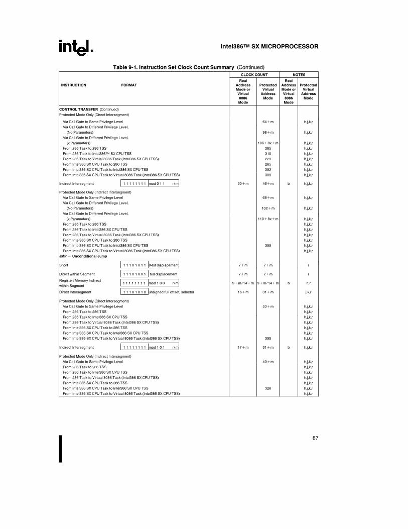
Intel386TM SX MICROPROCESSOR
Table 9-1. Instruction Set Clock Count Summary (Continued)
CLOCK COUNT NOTES
Real RealINSTRUCTION FORMAT Address Protected Address Protected
Mode or Virtual Mode or VirtualVirtual Address Virtual Address8086 Mode 8086 ModeMode Mode
CONTROL TRANSFER (Continued)
Protected Mode Only (Direct Intersegment)
Via Call Gate to Same Privilege Level 64am h,j,k,r
Via Call Gate to Different Privilege Level,
(No Parameters) 98am h,j,k,r
Via Call Gate to Different Privilege Level,
(x Parameters) 106a8xam h,j,k,r
From 286 Task to 286 TSS 285 h,j,k,r
From 286 Task to Intel386TM SX CPU TSS 310 h,j,k,r
From 286 Task to Virtual 8086 Task (Intel386 SX CPU TSS) 229 h,j,k,r
From Intel386 SX CPU Task to 286 TSS 285 h,j,k,r
From Intel386 SX CPU Task to Intel386 SX CPU TSS 392 h,j,k,r
From Intel386 SX CPU Task to Virtual 8086 Task (Intel386 SX CPU TSS) 309 h,j,k,r
Indirect Intersegment 1 1 1 1 1 1 1 1 mod 0 1 1 r/m 30am 46am b h,j,k,r
Protected Mode Only (Indirect Intersegment)
Via Call Gate to Same Privilege Level 68am h,j,k,r
Via Call Gate to Different Privilege Level,
(No Parameters) 102am h,j,k,r
Via Call Gate to Different Privilege Level,
(x Parameters) 110a8xam h,j,k,r
From 286 Task to 286 TSS h,j,k,r
From 286 Task to Intel386 SX CPU TSS h,j,k,r
From 286 Task to Virtual 8086 Task (Intel386 SX CPU TSS) h,j,k,r
From Intel386 SX CPU Task to 286 TSS h,j,k,r
From Intel386 SX CPU Task to Intel386 SX CPU TSS 399 h,j,k,r
From Intel386 SX CPU Task to Virtual 8086 Task (Intel386 SX CPU TSS) h,j,k,r
JMP e Unconditional Jump
Short 1 1 1 0 1 0 1 1 8-bit displacement 7am 7am r
Direct within Segment 1 1 1 0 1 0 0 1 full displacement 7am 7am r
within Segment
Register/Memory Indirect1 1 1 1 1 1 1 1 mod 1 0 0 r/m 9am/14am 9am/14am b h,r
Direct Intersegment 1 1 1 0 1 0 1 0 unsigned full offset, selector 16am 31am j,k,r
Protected Mode Only (Direct Intersegment)
Via Call Gate to Same Privilege Level 53am h,j,k,r
From 286 Task to 286 TSS h,j,k,r
From 286 Task to Intel386 SX CPU TSS h,j,k,r
From 286 Task to Virtual 8086 Task (Intel386 SX CPU TSS) h,j,k,r
From Intel386 SX CPU Task to 286 TSS h,j,k,r
From Intel386 SX CPU Task to Intel386 SX CPU TSS h,j,k,r
From Intel386 SX CPU Task to Virtual 8086 Task (Intel386 SX CPU TSS) 395 h,j,k,r
Indirect Intersegment 1 1 1 1 1 1 1 1 mod 1 0 1 r/m 17am 31am b h,j,k,r
Protected Mode Only (Indirect Intersegment)
Via Call Gate to Same Privilege Level 49am h,j,k,r
From 286 Task to 286 TSS h,j,k,r
From 286 Task to Intel386 SX CPU TSS h,j,k,r
From 286 Task to Virtual 8086 Task (Intel386 SX CPU TSS) h,j,k,r
From Intel386 SX CPU Task to 286 TSS h,j,k,r
From Intel386 SX CPU Task to Intel386 SX CPU TSS 328 h,j,k,r
From Intel386 SX CPU Task to Virtual 8086 Task (Intel386 SX CPU TSS) h,j,k,r
87

Intel386TM SX MICROPROCESSOR
Table 9-1. Instruction Set Clock Count Summary (Continued)
CLOCK COUNT NOTES
Real RealINSTRUCTION FORMAT Address Protected Address Protected
Mode or Virtual Mode or VirtualVirtual Address Virtual Address8086 Mode 8086 ModeMode Mode
CONTROL TRANSFER (Continued)
RET e Return from CALL:
Within Segment 1 1 0 0 0 0 1 1 12am b g, h, r
Within Segment Adding Immediate to SP 1 1 0 0 0 0 1 0 16-bit displ 12am b g, h, r
Intersegment 1 1 0 0 1 0 1 1 36am b g, h, j, k, r
Intersegment Adding Immediate to SP 1 1 0 0 1 0 1 0 16-bit displ 36am b g, h, j, k, r
Protected Mode Only (RET):
to Different Privilege Level
Intersegment 72 h, j, k, r
Intersegment Adding Immediate to SP 72 h, j, k, r
CONDITIONAL JUMPS
NOTE: Times Are Jump ‘‘Taken or Not Taken’’
JO e Jump on Overflow
8-Bit Displacement 0 1 1 1 0 0 0 0 8-bit displ 7am or 3 7am or 3 r
Full Displacement 0 0 0 0 1 1 1 1 1 0 0 0 0 0 0 0 full displacement 7am or 3 7am or 3 r
JNO e Jump on Not Overflow
8-Bit Displacement 0 1 1 1 0 0 0 1 8-bit displ 7am or 3 7am or 3 r
Full Displacement 0 0 0 0 1 1 1 1 1 0 0 0 0 0 0 1 full displacement 7am or 3 7am or 3 r
JB/JNAE e Jump on Below/Not Above or Equal
8-Bit Displacement 0 1 1 1 0 0 1 0 8-bit displ 7am or 3 7am or 3 r
Full Displacement 0 0 0 0 1 1 1 1 1 0 0 0 0 0 1 0 full displacement 7am or 3 7am or 3 r
JNB/JAE e Jump on Not Below/Above or Equal
8-Bit Displacement 0 1 1 1 0 0 1 1 8-bit displ 7am or 3 7am or 3 r
Full Displacement 0 0 0 0 1 1 1 1 1 0 0 0 0 0 1 1 full displacement 7am or 3 7am or 3 r
JE/JZ e Jump on Equal/Zero
8-Bit Displacement 0 1 1 1 0 1 0 0 8-bit displ 7am or 3 7am or 3 r
Full Displacement 0 0 0 0 1 1 1 1 1 0 0 0 0 1 0 0 full displacement 7am or 3 7am or 3 r
JNE/JNZ e Jump on Not Equal/Not Zero
8-Bit Displacement 0 1 1 1 0 1 0 1 8-bit displ 7am or 3 7am or 3 r
Full Displacement 0 0 0 0 1 1 1 1 1 0 0 0 0 1 0 1 full displacement 7am or 3 7am or 3 r
JBE/JNA e Jump on Below or Equal/Not Above
8-Bit Displacement 0 1 1 1 0 1 1 0 8-bit displ 7am or 3 7am or 3 r
Full Displacement 0 0 0 0 1 1 1 1 1 0 0 0 0 1 1 0 full displacement 7am or 3 7am or 3 r
JNBE/JA e Jump on Not Below or Equal/Above
8-Bit Displacement 0 1 1 1 0 1 1 1 8-bit displ 7am or 3 7am or 3 r
Full Displacement 0 0 0 0 1 1 1 1 1 0 0 0 0 1 1 1 full displacement 7am or 3 7am or 3 r
JS e Jump on Sign
8-Bit Displacement 0 1 1 1 1 0 0 0 8-bit displ 7am or 3 7am or 3 r
Full Displacement 0 0 0 0 1 1 1 1 1 0 0 0 1 0 0 0 full displacement 7am or 3 7am or 3 r
88

Intel386TM SX MICROPROCESSOR
Table 9-1. Instruction Set Clock Count Summary (Continued)
CLOCK COUNT NOTES
Real RealINSTRUCTION FORMAT Address Protected Address Protected
Mode or Virtual Mode or VirtualVirtual Address Virtual Address8086 Mode 8086 ModeMode Mode
CONDITIONAL JUMPS (Continued)
JNS e Jump on Not Sign
8-Bit Displacement 0 1 1 1 1 0 0 1 8-bit displ 7am or 3 7am or 3 r
Full Displacement 0 0 0 0 1 1 1 1 1 0 0 0 1 0 0 1 full displacement 7am or 3 7am or 3 r
JP/JPE e Jump on Parity/Parity Even
8-Bit Displacement 0 1 1 1 1 0 1 0 8-bit displ 7am or 3 7am or 3 r
Full Displacement 0 0 0 0 1 1 1 1 1 0 0 0 1 0 1 0 full displacement 7am or 3 7am or 3 r
JNP/JPO e Jump on Not Parity/Parity Odd
8-Bit Displacement 0 1 1 1 1 0 1 1 8-bit displ 7am or 3 7am or 3 r
Full Displacement 0 0 0 0 1 1 1 1 1 0 0 0 1 0 1 1 full displacement 7am or 3 7am or 3 r
JL/JNGE e Jump on Less/Not Greater or Equal
8-Bit Displacement 0 1 1 1 1 1 0 0 8-bit displ 7am or 3 7am or 3 r
Full Displacement 0 0 0 0 1 1 1 1 1 0 0 0 1 1 0 0 full displacement 7am or 3 7am or 3 r
JNL/JGE e Jump on Not Less/Greater or Equal
8-Bit Displacement 0 1 1 1 1 1 0 1 8-bit displ 7am or 3 7am or 3 r
Full Displacement 0 0 0 0 1 1 1 1 1 0 0 0 1 1 0 1 full displacement 7am or 3 7am or 3 r
JLE/JNG e Jump on Less or Equal/Not Greater
8-Bit Displacement 0 1 1 1 1 1 1 0 8-bit displ 7am or 3 7am or 3 r
Full Displacement 0 0 0 0 1 1 1 1 1 0 0 0 1 1 1 0 full displacement 7am or 3 7am or 3 r
JNLE/JG e Jump on Not Less or Equal/Greater
8-Bit Displacement 0 1 1 1 1 1 1 1 8-bit displ 7am or 3 7am or 3 r
Full Displacement 0 0 0 0 1 1 1 1 1 0 0 0 1 1 1 1 full displacement 7am or 3 7am or 3 r
JCXZ e Jump on CX Zero 1 1 1 0 0 0 1 1 8-bit displ 9am or 5 9am or 5 r
JECXZ e Jump on ECX Zero 1 1 1 0 0 0 1 1 8-bit displ 9am or 5 9am or 5 r
(Address Size Prefix Differentiates JCXZ from JECXZ)
LOOP e Loop CX Times 1 1 1 0 0 0 1 0 8-bit displ 11am 11am r
LOOPZ/LOOPE e Loop withZero/Equal 1 1 1 0 0 0 0 1 8-bit displ 11am 11am r
LOOPNZ/LOOPNE e Loop WhileNot Zero 1 1 1 0 0 0 0 0 8-bit displ 11am 11am r
CONDITIONAL BYTE SET
NOTE: Times Are Register/Memory
SETO e Set Byte on Overflow
To Register/Memory 0 0 0 0 1 1 1 1 1 0 0 1 0 0 0 0 mod 0 0 0 r/m 4/5* 4/5* h
SETNO e Set Byte on Not Overflow
To Register/Memory 0 0 0 0 1 1 1 1 1 0 0 1 0 0 0 1 mod 0 0 0 r/m 4/5* 4/5* h
SETB/SETNAE e Set Byte on Below/Not Above or Equal
To Register/Memory 0 0 0 0 1 1 1 1 1 0 0 1 0 0 1 0 mod 0 0 0 r/m 4/5* 4/5* h
89

Intel386TM SX MICROPROCESSOR
Table 9-1. Instruction Set Clock Count Summary (Continued)
CLOCK COUNT NOTES
Real RealINSTRUCTION FORMAT Address Protected Address Protected
Mode or Virtual Mode or VirtualVirtual Address Virtual Address8086 Mode 8086 ModeMode Mode
CONDITIONAL BYTE SET (Continued)
SETNB e Set Byte on Not Below/Above or Equal
To Register/Memory 0 0 0 0 1 1 1 1 1 0 0 1 0 0 1 1 mod 0 0 0 r/m 4/5* 4/5* h
SETE/SETZ e Set Byte on Equal/Zero
To Register/Memory 0 0 0 0 1 1 1 1 1 0 0 1 0 1 0 0 mod 0 0 0 r/m 4/5* 4/5* h
SETNE/SETNZ e Set Byte on Not Equal/Not Zero
To Register/Memory 0 0 0 0 1 1 1 1 1 0 0 1 0 1 0 1 mod 0 0 0 r/m 4/5* 4/5* h
SETBE/SETNA e Set Byte on Below or Equal/Not Above
To Register/Memory 0 0 0 0 1 1 1 1 1 0 0 1 0 1 1 0 mod 0 0 0 r/m 4/5* 4/5* h
SETNBE/SETA e Set Byte on Not Below or Equal/Above
To Register/Memory 0 0 0 0 1 1 1 1 1 0 0 1 0 1 1 1 mod 0 0 0 r/m 4/5* 4/5* h
SETS e Set Byte on Sign
To Register/Memory 0 0 0 0 1 1 1 1 1 0 0 1 1 0 0 0 mod 0 0 0 r/m 4/5* 4/5* h
SETNS e Set Byte on Not Sign
To Register/Memory 0 0 0 0 1 1 1 1 1 0 0 1 1 0 0 1 mod 0 0 0 r/m 4/5* 4/5* h
SETP/SETPE e Set Byte on Parity/Parity Even
To Register/Memory 0 0 0 0 1 1 1 1 1 0 0 1 1 0 1 0 mod 0 0 0 r/m 4/5* 4/5* h
SETNP/SETPO e Set Byte on Not Parity/Parity Odd
To Register/Memory 0 0 0 0 1 1 1 1 1 0 0 1 1 0 1 1 mod 0 0 0 r/m 4/5* 4/5* h
SETL/SETNGE e Set Byte on Less/Not Greater or Equal
To Register/Memory 0 0 0 0 1 1 1 1 1 0 0 1 1 1 0 0 mod 0 0 0 r/m 4/5* 4/5* h
SETNL/SETGE e Set Byte on Not Less/Greater or Equal
To Register/Memory 0 0 0 0 1 1 1 1 0 1 1 1 1 1 0 1 mod 0 0 0 r/m 4/5* 4/5* h
SETLE/SETNG e Set Byte on Less or Equal/Not Greater
To Register/Memory 0 0 0 0 1 1 1 1 1 0 0 1 1 1 1 0 mod 0 0 0 r/m 4/5* 4/5* h
SETNLE/SETG e Set Byte on Not Less or Equal/Greater
To Register/Memory 0 0 0 0 1 1 1 1 1 0 0 1 1 1 1 1 mod 0 0 0 r/m 4/5* 4/5* h
ENTER e Enter Procedure 1 1 0 0 1 0 0 0 16-bit displacement, 8-bit level
L e 0 10 10 b h
L e 1 14 14 b h
L l 1 17 a 17 a b h
8(n b 1) 8(n b 1)
LEAVE e Leave Procedure 1 1 0 0 1 0 0 1 4 4 b h
90

Intel386TM SX MICROPROCESSOR
Table 9-1. Instruction Set Clock Count Summary (Continued)
CLOCK COUNT NOTES
Real RealINSTRUCTION FORMAT Address Protected Address Protected
Mode or Virtual Mode or VirtualVirtual Address Virtual Address8086 Mode 8086 ModeMode Mode
INTERRUPT INSTRUCTIONS
INT e Interrupt:
Type Specified 1 1 0 0 1 1 0 1 type 37 b
Type 3 1 1 0 0 1 1 0 0 33 b
INTO e Interrupt 4 if Overflow Flag Set 1 1 0 0 1 1 1 0
If OF e 1 35 b, e
If OF e 0 3 3 b, e
Bound e Interrupt 5 if Detect Value 0 1 1 0 0 0 1 0 mod reg r/m
Out of Range
If Out of Range 44 b, e e, g, h, j, k, r
If In Range 10 10 b, e e, g, h, j, k, r
Protected Mode Only (INT)
INT: Type Specified
Via Interrupt or Trap Gate
Via Interrupt or Trap Gate
to Same Privilege Level 71 g, j, k, r
to Different Privilege Level 111 g, j, k, r
From 286 Task to 286 TSS via Task Gate 438 g, j, k, r
From 286 Task to Intel386TM SX CPU TSS via Task Gate 465 g, j, k, r
From 286 Task to virt 8086 md via Task Gate 382 g, j, k, r
From Intel386TM SX CPU Task to 286 TSS via Task Gate 440 g, j, k, r
From Intel386TM SX CPU Task to Intel386TM SX CPU TSS via Task Gate 467 g, j, k, r
From Intel386TM SX CPU Task to virt 8086 md via Task Gate 384 g, j, k, r
From virt 8086 md to 286 TSS via Task Gate 445 g, j, k, r
From virt 8086 md to Intel386TM SX CPU TSS via Task Gate 472 g, j, k, r
From virt 8086 md to priv level 0 via Trap Gate or Interrupt Gate 275
INT: TYPE 3
Via Interrupt or Trap Gate
to Same Privilege Level 71 g, j, k, r
Via Interrupt or Trap Gate
to Different Privilege Level 111 g, j, k, r
From 286 Task to 286 TSS via Task Gate 382 g, j, k, r
From 286 Task to Intel386TM SX CPU TSS via Task Gate 409 g, j, k, r
From 286 Task to Virt 8086 md via Task Gate 326 g, j, k, r
From Intel386TM SX CPU Task to 286 TSS via Task Gate 384 g, j, k, r
From Intel386TM SX CPU Task to Intel386TM SX CPU TSS via Task Gate 411 g, j, k, r
From Intel386TM SX CPU Task to Virt 8086 md via Task Gate 328 g, j, k, r
From virt 8086 md to 286 TSS via Task Gate 389 g, j, k, r
From virt 8086 md to Intel386TM SX CPU TSS via Task Gate 416 g, j, k, r
From virt 8086 md to priv level 0 via Trap Gate or Interrupt Gate 223
INTO:
Via Interrupt or Trap Grate
to Same Privilege Level 71 g, j, k, r
Via Interrupt or Trap Gate
to Different Privilege Level 111 g, j, k, r
From 286 Task to 286 TSS via Task Gate 384 g, j, k, r
From 286 Task to Intel386TM SX CPU TSS via Task Gate 411 g, j, k, r
From 286 Task to virt 8086 md via Task Gate 328 g, j, k, r
From Intel386TM SX CPU Task to 286 TSS via Task Gate Intel386 DX g, j, k, r
From Intel386TM SX CPU Task to Intel386TM SX CPU TSS via Task Gate 413 g, j, k, r
From Intel386TM SX CPU Task to virt 8086 md via Task Gate 329 g, j, k, r
From virt 8086 md to 286 TSS via Task Gate 391 g, j, k, r
From virt 8086 md to Intel386TM SX CPU TSS via Task Gate 418 g, j, k, r
From virt 8086 md to priv level 0 via Trap Gate or Interrupt Gate 223
91

Intel386TM SX MICROPROCESSOR
Table 9-1. Instruction Set Clock Count Summary (Continued)
CLOCK COUNT NOTES
Real RealINSTRUCTION FORMAT Address Protected Address Protected
Mode or Virtual Mode or VirtualVirtual Address Virtual Address8086 Mode 8086 ModeMode Mode
INTERRUPT INSTRUCTIONS (Continued)
BOUND:
Via Interrupt or Trap Gate
to Same Privilege Level 71 g, j, k, r
Via Interrupt or Trap Gate
to Different Privilege Level 111 g, j, k, r
From 286 Task to 286 TSS via Task Gate 358 g, j, k, r
From 286 Task to Intel386TM SX CPU TSS via Task Gate 388 g, j, k, r
From 268 Task to virt 8086 Mode via Task Gate 335 g, j, k, r
From Intel386 SX CPU Task to 286 TSS via Task Gate 368 g, j, k, r
From Intel386 SX CPU Task to Intel386 SX CPU TSS via Task Gate 398 g, j, k, r
From Intel386 SX CPU Task to virt 8086 Mode via Task Gate 347 g, j, k, r,
From virt 8086 Mode to 286 TSS via Task Gate 368 g, j, k, r
From virt 8086 Mode to Intel386 SX CPU TSS via Task Gate 398 g, j, k, r
From virt 8086 md to priv level 0 via Trap Gate or Interrupt Gate 223
INTERRUPT RETURN
IRET e Interrupt Return 1 1 0 0 1 1 1 1 24 g, h, j, k, r
Protected Mode Only (IRET)
To the Same Privilege Level (within task) 42 g, h, j, k, r
To Different Privilege Level (within task) 86 g, h, j, k, r
From 286 Task to 286 TSS 285 h, j, k, r
From 286 Task to Intel386 SX CPU TSS 318 h, j, k, r
From 286 Task to Virtual 8086 Task 267 h, j, k, r
From 286 Task to Virtual 8086 Mode (within task) 113
From Intel386 SX CPU Task to 286 TSS 324 h, j, k, r
From Intel386 SX CPU Task to Intel386 SX CPU TSS 328 h, j, k, r
From Intel386 SX CPU Task to Virtual 8086 Task 377 h, j, k, r
From Intel386 SX CPU Task to Virtual 8086 Mode (within task) 113
PROCESSOR CONTROL
HLT e HALT 1 1 1 1 0 1 0 0 5 5 l
MOV e Move to and From Control/Debug/Test Registers
CR0/CR2/CR3 from register 0 0 0 0 1 1 1 1 0 0 1 0 0 0 1 0 1 1 eee reg 10/4/5 10/4/5 l
Register From CR0–3 0 0 0 0 1 1 1 1 0 0 1 0 0 0 0 0 1 1 eee reg 6 6 l
DR0–3 From Register 0 0 0 0 1 1 1 1 0 0 1 0 0 0 1 1 1 1 eee reg 22 22 l
DR6–7 From Register 0 0 0 0 1 1 1 1 0 0 1 0 0 0 1 1 1 1 eee reg 16 16 l
Register from DR6–7 0 0 0 0 1 1 1 1 0 0 1 0 0 0 0 1 1 1 eee reg 14 14 l
Register from DR0–3 0 0 0 0 1 1 1 1 0 0 1 0 0 0 0 1 1 1 eee reg 22 22 l
TR6–7 from Register 0 0 0 0 1 1 1 1 0 0 1 0 0 1 1 0 1 1 eee reg 12 12 l
Register from TR6–7 0 0 0 0 1 1 1 1 0 0 1 0 0 1 0 0 1 1 eee reg 12 12 l
NOP e No Operation 1 0 0 1 0 0 0 0 3 3
WAITeWait until BUSYÝ pin is negated 1 0 0 1 1 0 1 1 6 6
92
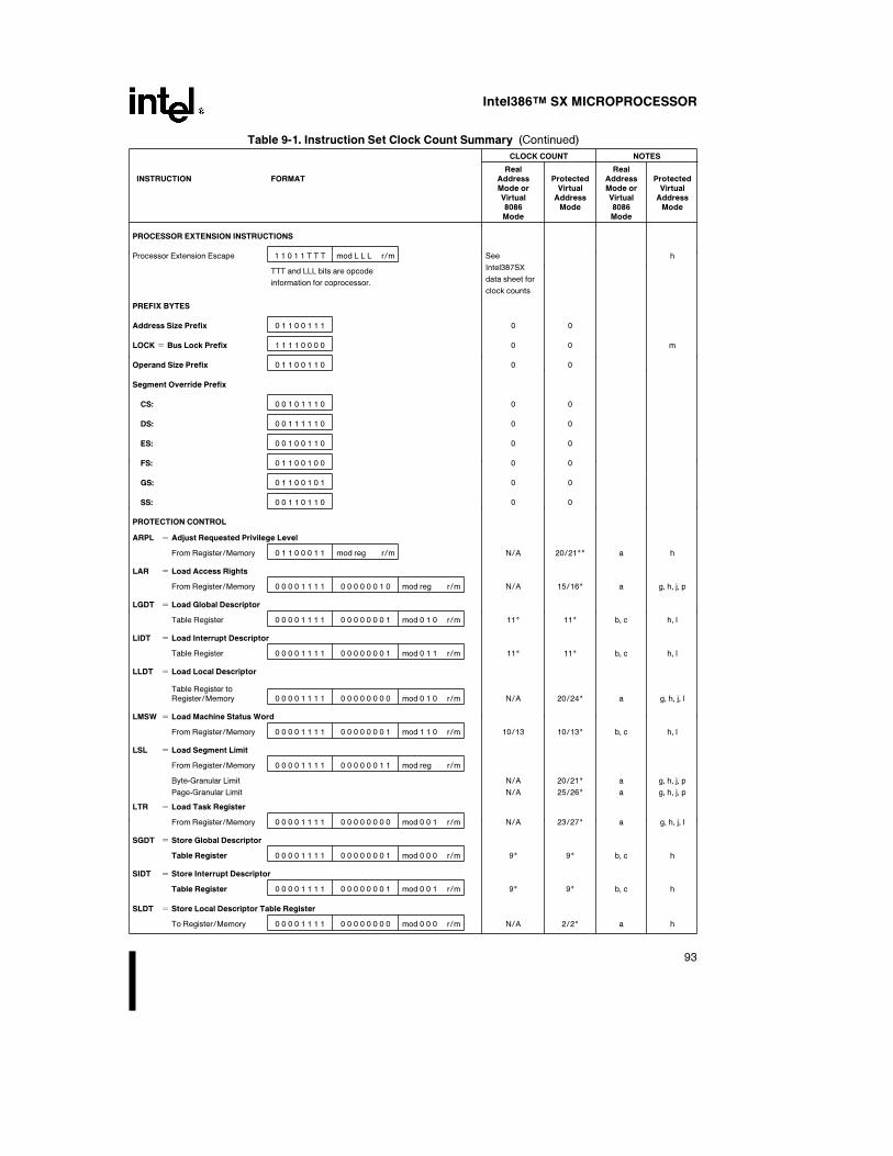
Intel386TM SX MICROPROCESSOR
Table 9-1. Instruction Set Clock Count Summary (Continued)
CLOCK COUNT NOTES
Real RealINSTRUCTION FORMAT Address Protected Address Protected
Mode or Virtual Mode or VirtualVirtual Address Virtual Address8086 Mode 8086 ModeMode Mode
PROCESSOR EXTENSION INSTRUCTIONS
Processor Extension Escape 1 1 0 1 1 T T T mod L L L r/m See h
TTT and LLL bits are opcode Intel387SX
information for coprocessor. data sheet for
clock counts
PREFIX BYTES
Address Size Prefix 0 1 1 0 0 1 1 1 0 0
LOCK e Bus Lock Prefix 1 1 1 1 0 0 0 0 0 0 m
Operand Size Prefix 0 1 1 0 0 1 1 0 0 0
Segment Override Prefix
CS: 0 0 1 0 1 1 1 0 0 0
DS: 0 0 1 1 1 1 1 0 0 0
ES: 0 0 1 0 0 1 1 0 0 0
FS: 0 1 1 0 0 1 0 0 0 0
GS: 0 1 1 0 0 1 0 1 0 0
SS: 0 0 1 1 0 1 1 0 0 0
PROTECTION CONTROL
ARPL e Adjust Requested Privilege Level
From Register/Memory 0 1 1 0 0 0 1 1 mod reg r/m N/A 20/21** a h
LAR e Load Access Rights
From Register/Memory 0 0 0 0 1 1 1 1 0 0 0 0 0 0 1 0 mod reg r/m N/A 15/16* a g, h, j, p
LGDT e Load Global Descriptor
Table Register 0 0 0 0 1 1 1 1 0 0 0 0 0 0 0 1 mod 0 1 0 r/m 11* 11* b, c h, l
LIDT e Load Interrupt Descriptor
Table Register 0 0 0 0 1 1 1 1 0 0 0 0 0 0 0 1 mod 0 1 1 r/m 11* 11* b, c h, l
LLDT e Load Local Descriptor
Table Register toRegister/Memory 0 0 0 0 1 1 1 1 0 0 0 0 0 0 0 0 mod 0 1 0 r/m N/A 20/24* a g, h, j, l
LMSW e Load Machine Status Word
From Register/Memory 0 0 0 0 1 1 1 1 0 0 0 0 0 0 0 1 mod 1 1 0 r/m 10/13 10/13* b, c h, l
LSL e Load Segment Limit
From Register/Memory 0 0 0 0 1 1 1 1 0 0 0 0 0 0 1 1 mod reg r/m
Byte-Granular Limit N/A 20/21* a g, h, j, p
Page-Granular Limit N/A 25/26* a g, h, j, p
LTR e Load Task Register
From Register/Memory 0 0 0 0 1 1 1 1 0 0 0 0 0 0 0 0 mod 0 0 1 r/m N/A 23/27* a g, h, j, l
SGDT e Store Global Descriptor
Table Register 0 0 0 0 1 1 1 1 0 0 0 0 0 0 0 1 mod 0 0 0 r/m 9* 9* b, c h
SIDT e Store Interrupt Descriptor
Table Register 0 0 0 0 1 1 1 1 0 0 0 0 0 0 0 1 mod 0 0 1 r/m 9* 9* b, c h
SLDT e Store Local Descriptor Table Register
To Register/Memory 0 0 0 0 1 1 1 1 0 0 0 0 0 0 0 0 mod 0 0 0 r/m N/A 2/2* a h
93

Intel386TM SX MICROPROCESSOR
Table 9-1. Instruction Set Clock Count Summary (Continued)
CLOCK COUNT NOTES
Real RealINSTRUCTION FORMAT Address Protected Address Protected
Mode or Virtual Mode or VirtualVirtual Address Virtual Address8086 Mode 8086 ModeMode Mode
PROTECTION CONTROL (Continued)
SMSW eStore MachineStatus Word 0 0 0 0 1 1 1 1 0 0 0 0 0 0 0 1 mod 1 0 0 r/m 2/2* 2/2* b, c h, l
STR eStore Task Register
To Register/Memory 0 0 0 0 1 1 1 1 0 0 0 0 0 0 0 0 mod 0 0 1 r/m N/A 2/2* a h
VERR eVerify Read Access
Register/Memory 0 0 0 0 1 1 1 1 0 0 0 0 0 0 0 0 mod 1 0 0 r/m N/A 10/11* a g, h, j, p
VERW e Verify Write Access 0 0 0 0 1 1 1 1 0 0 0 0 0 0 0 0 mod 1 0 1 r/m N/A 15/16* a g, h, j, p
INSTRUCTION NOTES FOR TABLE 9-1
Notes a through c apply to Real Address Mode only:a. This is a Protected Mode instruction. Attempted execution in Real Mode will result in exception 6 (invalid opcode).b. Exception 13 fault (general protection) will occur in Real Mode if an operand reference is made that partially or fullyextends beyond the maximum CS, DS, ES, FS or GS limit, FFFFH. Exception 12 fault (stack segment limit violation or notpresent) will occur in Real Mode if an operand reference is made that partially or fully extends beyond the maximum SS limit.c. This instruction may be executed in Real Mode. In Real Mode, its purpose is primarily to initialize the CPU for ProtectedMode.
Notes d through g apply to Real Address Mode and Protected Virtual Address Mode:d. The Intel386 SX CPU uses an early-out multiply algorithm. The actual number of clocks depends on the position of themost significant bit in the operand (multiplier).
Clock counts given are minimum to maximum. To calculate actual clocks use the following formula:Actual Clock e if m k l 0 then max ([log2 lml], 3) a b clocks:
if m e 0 then 3ab clocksIn this formula, m is the multiplier, andb e 9 for register to register,b e 12 for memory to register,b e 10 for register with immediate to register,b e 11 for memory with immediate to register.
e. An exception may occur, depending on the value of the operand.f. LOCKÝ is automatically asserted, regardless of the presence or absence of the LOCKÝ prefix.g. LOCKÝ is asserted during descriptor table accesses.
Notes h through s/t apply to Protected Virtual Address Mode only:h. Exception 13 fault (general protection violation) will occur if the memory operand in CS, DS, ES, FS or GS cannot be useddue to either a segment limit violation or access rights violation. If a stack limit is violated, an exception 12 (stack segmentlimit violation or not present) occurs.i. For segment load operations, the CPL, RPL, and DPL must agree with the privilege rules to avoid an exception 13 fault(general protection violation). The segment’s descriptor must indicate ‘‘present’’ or exception 11 (CS, DS, ES, FS, GS notpresent). If the SS register is loaded and a stack segment not present is detected, an exception 12 (stack segment limitviolation or not present) occurs.j. All segment descriptor accesses in the GDT or LDT made by this instruction will automatically assert LOCKÝ to maintaindescriptor integrity in multiprocessor systems.k. JMP, CALL, INT, RET and IRET instructions referring to another code segment will cause an exception 13 (generalprotection violation) if an applicable privilege rule is violated.l. An exception 13 fault occurs if CPL is greater than 0 (0 is the most privileged level).m. An exception 13 fault occurs if CPL is greater than IOPL.n. The IF bit of the flag register is not updated if CPL is greater than IOPL. The IOPL and VM fields of the flag register areupdated only if CPL e 0.o. The PE bit of the MSW (CR0) cannot be reset by this instruction. Use MOV into CR0 if desiring to reset the PE bit.p. Any violation of privilege rules as applied to the selector operand does not cause a protection exception; rather, the zeroflag is cleared.q. If the coprocessor’s memory operand violates a segment limit or segment access rights, an exception 13 fault (generalprotection exception) will occur before the ESC instruction is executed. An exception 12 fault (stack segment limit violationor not present) will occur if the stack limit is violated by the operand’s starting address.r. The destination of a JMP, CALL, INT, RET or IRET must be in the defined limit of a code segment or an exception 13 fault(general protection violation) will occur.s/t. The instruction will execute in s clocks if CPL s IOPL. If CPL l IOPL, the instruction will take t clocks.
94
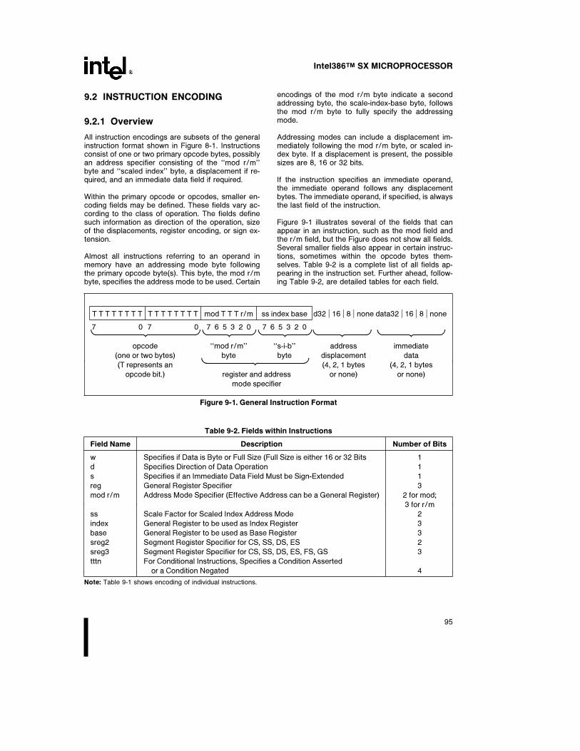
Intel386TM SX MICROPROCESSOR
9.2 INSTRUCTION ENCODING
9.2.1 Overview
All instruction encodings are subsets of the generalinstruction format shown in Figure 8-1. Instructionsconsist of one or two primary opcode bytes, possiblyan address specifier consisting of the ‘‘mod r/m’’byte and ‘‘scaled index’’ byte, a displacement if re-quired, and an immediate data field if required.
Within the primary opcode or opcodes, smaller en-coding fields may be defined. These fields vary ac-cording to the class of operation. The fields definesuch information as direction of the operation, sizeof the displacements, register encoding, or sign ex-tension.
Almost all instructions referring to an operand inmemory have an addressing mode byte followingthe primary opcode byte(s). This byte, the mod r/mbyte, specifies the address mode to be used. Certain
encodings of the mod r/m byte indicate a secondaddressing byte, the scale-index-base byte, followsthe mod r/m byte to fully specify the addressingmode.
Addressing modes can include a displacement im-mediately following the mod r/m byte, or scaled in-dex byte. If a displacement is present, the possiblesizes are 8, 16 or 32 bits.
If the instruction specifies an immediate operand,the immediate operand follows any displacementbytes. The immediate operand, if specified, is alwaysthe last field of the instruction.
Figure 9-1 illustrates several of the fields that canappear in an instruction, such as the mod field andthe r/m field, but the Figure does not show all fields.Several smaller fields also appear in certain instruc-tions, sometimes within the opcode bytes them-selves. Table 9-2 is a complete list of all fields ap-pearing in the instruction set. Further ahead, follow-ing Table 9-2, are detailed tables for each field.
T T T T T T T T T T T T T T T T mod T T T r/m ss index base d32 l 16 l 8 l none data32 l 16 l 8 l none
7 0 7 0 7 6 5 3 2 0 7 6 5 3 2 0X ä Y X ä Y X ä YX ä Y X ä Yopcode ‘‘mod r/m’’ ‘‘s-i-b’’ address immediate
(one or two bytes) byte byte displacement dataX ä Y(T represents an (4, 2, 1 bytes (4, 2, 1 bytes
opcode bit.) register and address or none) or none)
mode specifier
Figure 9-1. General Instruction Format
Table 9-2. Fields within Instructions
Field Name Description Number of Bits
w Specifies if Data is Byte or Full Size (Full Size is either 16 or 32 Bits 1
d Specifies Direction of Data Operation 1
s Specifies if an Immediate Data Field Must be Sign-Extended 1
reg General Register Specifier 3
mod r/m Address Mode Specifier (Effective Address can be a General Register) 2 for mod;
3 for r/m
ss Scale Factor for Scaled Index Address Mode 2
index General Register to be used as Index Register 3
base General Register to be used as Base Register 3
sreg2 Segment Register Specifier for CS, SS, DS, ES 2
sreg3 Segment Register Specifier for CS, SS, DS, ES, FS, GS 3
tttn For Conditional Instructions, Specifies a Condition Asserted
or a Condition Negated 4
Note: Table 9-1 shows encoding of individual instructions.
95

Intel386TM SX MICROPROCESSOR
9.2.2 32-Bit Extensions of theInstruction Set
With the Intel386 SX CPU, the 8086/80186/80286instruction set is extended in two orthogonal direc-tions: 32-bit forms of all 16-bit instructions are addedto support the 32-bit data types, and 32-bit address-ing modes are made available for all instructions ref-erencing memory. This orthogonal instruction set ex-tension is accomplished having a Default (D) bit inthe code segment descriptor, and by having 2 prefix-es to the instruction set.
Whether the instruction defaults to operations of16 bits or 32 bits depends on the setting of the D bitin the code segment descriptor, which gives the de-fault length (either 32 bits or 16 bits) for both oper-ands and effective addresses when executing thatcode segment. In the Real Address Mode or Virtual8086 Mode, no code segment descriptors are used,but a D value of 0 is assumed internally by theIntel386 SX CPU when operating in those modes(for 16-bit default sizes compatible with the 8086/80186/80286).
Two prefixes, the Operand Size Prefix and the Effec-tive Address Size Prefix, allow overriding individuallythe Default selection of operand size and effectiveaddress size. These prefixes may precede any op-code bytes and affect only the instruction they pre-cede. If necessary, one or both of the prefixes maybe placed before the opcode bytes. The presence ofthe Operand Size Prefix and the Effective AddressPrefix will toggle the operand size or the effectiveaddress size, respectively, to the value ‘‘opposite’’from the Default setting. For example, if the defaultoperand size is for 32-bit data operations, then pres-ence of the Operand Size Prefix toggles the instruc-tion to 16-bit data operation. As another example, ifthe default effective address size is 16 bits, pres-ence of the Effective Address Size prefix toggles theinstruction to use 32-bit effective address computa-tions.
These 32-bit extensions are available in all modes,including the Real Address Mode or the Virtual 8086Mode. In these modes the default is always 16 bits,so prefixes are needed to specify 32-bit operands oraddresses. For instructions with more than one pre-fix, the order of prefixes is unimportant.
Unless specified otherwise, instructions with 8-bitand 16-bit operands do not affect the contents ofthe high-order bits of the extended registers.
9.2.3 Encoding of Instruction Fields
Within the instruction are several fields indicatingregister selection, addressing mode and so on. Theexact encodings of these fields are defined immedi-ately ahead.
9.2.3.1 ENCODING OF OPERAND LENGTH (w)FIELD
For any given instruction performing a data opera-tion, the instruction is executing as a 32-bit operationor a 16-bit operation. Within the constraints of theoperation size, the w field encodes the operand sizeas either one byte or the full operation size, asshown in the table below.
Operand Size Operand Size
w Field During 16-Bit During 32-Bit
Data Operations Data Operations
0 8 Bits 8 Bits
1 16 Bits 32 Bits
9.2.3.2 ENCODING OF THE GENERALREGISTER (reg) FIELD
The general register is specified by the reg field,which may appear in the primary opcode bytes, or asthe reg field of the ‘‘mod r/m’’ byte, or as the r/mfield of the ‘‘mod r/m’’ byte.
Encoding of reg Field When w Field
is not Present in Instruction
Register Selected Register Selected
reg Field During 16-Bit During 32-Bit
Data Operations Data Operations
000 AX EAX
001 CX ECX
010 DX EDX
011 BX EBX
100 SP ESP
101 BP EBP
101 SI ESI
101 DI EDI
Encoding of reg Field When w Field
is Present in Instruction
Register Specified by reg Field
During 16-Bit Data Operations:
regFunction of w Field
(when w e 0) (when w e 1)
000 AL AX
001 CL CX
010 DL DX
011 BL BX
100 AH SP
101 CH BP
110 DH SI
111 BH DI
96

Intel386TM SX MICROPROCESSOR
Register Specified by reg Field
During 32-Bit Data Operations
regFunction of w Field
(when w e 0) (when w e 1)
000 AL EAX
001 CL ECX
010 DL EDX
011 BL EBX
100 AH ESP
101 CH EBP
110 DH ESI
111 BH EDI
9.2.3.3 ENCODING OF THE SEGMENTREGISTER (sreg) FIELD
The sreg field in certain instructions is a 2-bit fieldallowing one of the four 80286 segment registers tobe specified. The sreg field in other instructions is a3-bit field, allowing the Intel386 SX CPU FS and GSsegment registers to be specified.
2-Bit sreg2 Field
2-BitSegment
sreg2 FieldRegister
Selected
00 ES
01 CS
10 SS
11 DS
3-Bit sreg3 Field
3-BitSegment
sreg3 FieldRegister
Selected
000 ES
001 CS
010 SS
011 DS
100 FS
101 GS
110 do not use
111 do not use
9.2.3.4 ENCODING OF ADDRESS MODE
Except for special instructions, such as PUSH orPOP, where the addressing mode is pre-determined,the addressing mode for the current instruction isspecified by addressing bytes following the primaryopcode. The primary addressing byte is the ‘‘modr/m’’ byte, and a second byte of addressing informa-tion, the ‘‘s-i-b’’ (scale-index-base) byte, can bespecified.
The s-i-b byte (scale-index-base byte) is specifiedwhen using 32-bit addressing mode and the ‘‘modr/m’’ byte has r/m e 100 and mod e 00, 01 or 10.When the sib byte is present, the 32-bit addressingmode is a function of the mod, ss, index, and basefields.
The primary addressing byte, the ‘‘mod r/m’’ byte,also contains three bits (shown as TTT in Figure 8-1)sometimes used as an extension of the primary op-code. The three bits, however, may also be used asa register field (reg).
When calculating an effective address, either 16-bitaddressing or 32-bit addressing is used. 16-bit ad-dressing uses 16-bit address components to calcu-late the effective address while 32-bit addressinguses 32-bit address components to calculate the ef-fective address. When 16-bit addressing is used, the‘‘mod r/m’’ byte is interpreted as a 16-bit addressingmode specifier. When 32-bit addressing is used, the‘‘mod r/m’’ byte is interpreted as a 32-bit addressingmode specifier.
Tables on the following three pages define all en-codings of all 16-bit addressing modes and 32-bitaddressing modes.
97

Intel386TM SX MICROPROCESSOR
Encoding of 16-bit Address Mode with ‘‘mod r/m’’ Byte
mod r/m Effective Address
00 000 DS:[BXaSI]00 001 DS:[BXaDI]00 010 SS:[BPaSI]00 011 SS:[BPaDI]00 100 DS:[SI]00 101 DS:[DI]00 110 DS:d16
00 111 DS:[BX]
01 000 DS:[BXaSIad8]01 001 DS:[BXaDIad8]01 010 SS:[BPaSIad8]01 011 SS:[BPaDIad8]01 100 DS:[SIad8]01 101 DS:[DIad8]01 110 SS:[BPad8]01 111 DS:[BXad8]
mod r/m Effective Address
10 000 DS:[BXaSIad16]10 001 DS:[BXaDIad16]10 010 SS:[BPaSIad16]10 011 SS:[BPaDIad16]10 100 DS:[SIad16]10 101 DS:[DIad16]10 110 SS:[BPad16]10 111 DS:[BXad16]
11 000 registerÐsee below
11 001 registerÐsee below
11 010 registerÐsee below
11 011 registerÐsee below
11 100 registerÐsee below
11 101 registerÐsee below
11 110 registerÐsee below
11 111 registerÐsee below
Register Specified by r/m
During 16-Bit Data Operations
mod r/mFunction of w Field
(when we0) (when w e1)
11 000 AL AX
11 001 CL CX
11 010 DL DX
11 011 BL BX
11 100 AH SP
11 101 CH BP
11 110 DH SI
11 111 BH DI
Register Specified by r/m
During 32-Bit Data Operations
mod r/mFunction of w Field
(when we0) (when w e1)
11 000 AL EAX
11 001 CL ECX
11 010 DL EDX
11 011 BL EBX
11 100 AH ESP
11 101 CH EBP
11 110 DH ESI
11 111 BH EDI
98

Intel386TM SX MICROPROCESSOR
Encoding of 32-bit Address Mode with ‘‘mod r/m’’ byte (no ‘‘s-i-b’’ byte present):
mod r/m Effective Address
00 000 DS:[EAX]00 001 DS:[ECX]00 010 DS:[EDX]00 011 DS:[EBX]00 100 s-i-b is present
00 101 DS:d32
00 110 DS:[ESI]00 111 DS:[EDI]
01 000 DS:[EAXad8]01 001 DS:[ECXad8]01 010 DS:[EDXad8]01 011 DS:[EBXad8]01 100 s-i-b is present
01 101 SS:[EBPad8]01 110 DS:[ESIad8]01 111 DS:[EDIad8]
mod r/m Effective Address
10 000 DS:[EAXad32]10 001 DS:[ECXad32]10 010 DS:[EDXad32]10 011 DS:[EBXad32]10 100 s-i-b is present
10 101 SS:[EBPad32]10 110 DS:[ESIad32]10 111 DS:[EDIad32]
11 000 registerÐsee below
11 001 registerÐsee below
11 010 registerÐsee below
11 011 registerÐsee below
11 100 registerÐsee below
11 101 registerÐsee below
11 110 registerÐsee below
11 111 registerÐsee below
Register Specified by reg or r/m
during 16-Bit Data Operations:
mod r/mfunction of w field
(when we0) (when we1)
11 000 AL AX
11 001 CL CX
11 010 DL DX
11 011 BL BX
11 100 AH SP
11 101 CH BP
11 110 DH SI
11 111 BH DI
Register Specified by reg or r/m
during 32-Bit Data Operations:
mod r/mfunction of w field
(when we0) (when we1)
11 000 AL EAX
11 001 CL ECX
11 010 DL EDX
11 011 BL EBX
11 100 AH ESP
11 101 CH EBP
11 110 DH ESI
11 111 BH EDI
99
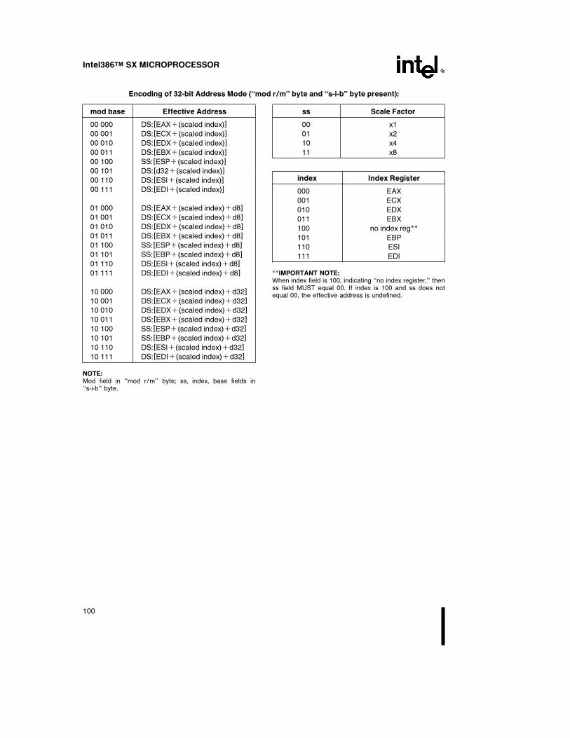
Intel386TM SX MICROPROCESSOR
Encoding of 32-bit Address Mode (‘‘mod r/m’’ byte and ‘‘s-i-b’’ byte present):
mod base Effective Address
00 000 DS:[EAXa(scaled index)]00 001 DS:[ECXa(scaled index)]00 010 DS:[EDXa(scaled index)]00 011 DS:[EBXa(scaled index)]00 100 SS:[ESPa(scaled index)]00 101 DS:[d32a(scaled index)]00 110 DS:[ESIa(scaled index)]00 111 DS:[EDIa(scaled index)]
01 000 DS:[EAXa(scaled index)ad8]01 001 DS:[ECXa(scaled index)ad8]01 010 DS:[EDXa(scaled index)ad8]01 011 DS:[EBXa(scaled index)ad8]01 100 SS:[ESPa(scaled index)ad8]01 101 SS:[EBPa(scaled index)ad8]01 110 DS:[ESIa(scaled index)ad8]01 111 DS:[EDIa(scaled index)ad8]
10 000 DS:[EAXa(scaled index)ad32]10 001 DS:[ECXa(scaled index)ad32]10 010 DS:[EDXa(scaled index)ad32]10 011 DS:[EBXa(scaled index)ad32]10 100 SS:[ESPa(scaled index)ad32]10 101 SS:[EBPa(scaled index)ad32]10 110 DS:[ESIa(scaled index)ad32]10 111 DS:[EDIa(scaled index)ad32]
NOTE:Mod field in ‘‘mod r/m’’ byte; ss, index, base fields in‘‘s-i-b’’ byte.
ss Scale Factor
00 x1
01 x2
10 x4
11 x8
index Index Register
000 EAX
001 ECX
010 EDX
011 EBX
100 no index reg**101 EBP
110 ESI
111 EDI
**IMPORTANT NOTE:When index field is 100, indicating ‘‘no index register,’’ thenss field MUST equal 00. If index is 100 and ss does notequal 00, the effective address is undefined.
100

Intel386TM SX MICROPROCESSOR
9.2.3.5 ENCODING OF OPERATION DIRECTION(d) FIELD
In many two-operand instructions the d field is pres-ent to indicate which operand is considered thesource and which is the destination.
d Direction of Operation
0 Register/Memory k- - Register‘‘reg’’ Field Indicates Source Operand;‘‘mod r/m’’ or ‘‘mod ss index base’’ IndicatesDestination Operand
1 Register k- - Register/Memory‘‘reg’’ Field Indicates Destination Operand;‘‘mod r/m’’ or ‘‘mod ss index base’’ IndicatesSource Operand
9.2.3.6 ENCODING OF SIGN-EXTEND (s) FIELD
The s field occurs primarily to instructions with im-mediate data fields. The s field has an effect only ifthe size of the immediate data is 8 bits and is beingplaced in a 16-bit or 32-bit destination.
sEffect on Effect on
Immediate Data8 Immediate Data 16l32
0 None None
1 Sign-Extend Data8 Noneto Fill 16-Bit or 32-BitDestination
9.2.3.7 ENCODING OF CONDITIONAL TEST(tttn) FIELD
For the conditional instructions (conditional jumpsand set on condition), tttn is encoded with n indicat-ing to use the condition (ne0) or its negation (ne1),and ttt giving the condition to test.
Mnemonic Condition tttn
O Overflow 0000NO No Overflow 0001B/NAE Below/Not Above or Equal 0010NB/AE Not Below/Above or Equal 0011E/Z Equal/Zero 0100NE/NZ Not Equal/Not Zero 0101BE/NA Below or Equal/Not Above 0110NBE/A Not Below or Equal/Above 0111S Sign 1000NS Not Sign 1001P/PE Parity/Parity Even 1010NP/PO Not Parity/Parity Odd 1011L/NGE Less Than/Not Greater or Equal 1100NL/GE Not Less Than/Greater or Equal 1101LE/NG Less Than or Equal/Greater Than 1110NLE/G Not Less or Equal/Greater Than 1111
9.2.3.8 ENCODING OF CONTROL OR DEBUGOR TEST REGISTER (eee) FIELD
For the loading and storing of the Control, Debugand Test registers.
When Interpreted as Control Register Field
eee Code Reg Name
000 CR0010 CR2011 CR3
Do not use any other encoding
When Interpreted as Debug Register Field
eee Code Reg Name
000 DR0001 DR1010 DR2011 DR3110 DR6111 DR7
Do not use any other encoding
When Interpreted as Test Register Field
eee Code Reg Name
110 TR6111 TR7
Do not use any other encoding
101

Intel386TM SX MICROPROCESSOR
DATA SHEET REVISION REVIEW
The following list represents key differences between this data sheet and the -007 version of the Intel386TM
SX microprocessor data sheet. Please review the summary carefully.
1. Table 5.7, E-Step revision identifier is added.
2. Table 7.3, ICC supply current for CLK2 e 40 MHz with 20 MHz Intel386 SX has a typical ICC of 180 mA.
3. Table 7.5, t4 CLK2 fall time and t5 CLK2 rise time have no minimum time for all speeds but maximum timefor all speeds is 8 ns.
4. Figure 7.11, CHMOS III characteristics for typical ICC has been taken out.
102