intel e8500 chipset external memory bridge (xmb) · 4.4.17 mc: memory control ... 4.4.26 cbc: chip...
TRANSCRIPT

Intel® E8500 Chipset eXternal Memory Bridge (XMB)Datasheet
March 2005
Document Number: 306746-001

2 Intel® E8500 Chipset eXternal Memory Bridge (XMB) Datasheet
INFORMATION IN THIS DOCUMENT IS PROVIDED IN CONNECTION WITH INTEL® PRODUCTS. NO LICENSE, EXPRESS OR IMPLIED, BY ESTOPPEL OR OTHERWISE, TO ANY INTELLECTUAL PROPERTY RIGHTS IS GRANTED BY THIS DOCUMENT. EXCEPT AS PROVIDED IN INTEL'S TERMS AND CONDITIONS OF SALE FOR SUCH PRODUCTS, INTEL ASSUMES NO LIABILITY WHATSOEVER, AND INTEL DISCLAIMS ANY EXPRESS OR IMPLIED WARRANTY, RELATING TO SALE AND/OR USE OF INTEL PRODUCTS INCLUDING LIABILITY OR WARRANTIES RELATING TO FITNESS FOR A PARTICULAR PURPOSE, MERCHANTABILITY, OR INFRINGEMENT OF ANY PATENT, COPYRIGHT OR OTHER INTELLECTUAL PROPERTY RIGHT. Intel products are not intended for use in medical, life saving, or life sustaining applications.
Intel may make changes to specifications and product descriptions at any time, without notice.
Designers must not rely on the absence or characteristics of any features or instructions marked "reserved" or "undefined." Intel reserves these for future definition and shall have no responsibility whatsoever for conflicts or incompatibilities arising from future changes to them.
The Intel® E8500 chipset eXternal Memory Bridge (XMB) chipset may contain design defects or errors known as errata which may cause the product to deviate from published specifications. Current characterized errata are available on request.
Contact your local Intel sales office or your distributor to obtain the latest specifications and before placing your product order.
I2C is a two-wire communications bus/protocol developed by Philips. SMBus is a subset of the I2C bus/protocol and was developed by Intel. Implementations of the I2C bus/protocol may require licenses from various entities, including Philips Electronics N.V. and North American Philips Corporation.
Intel, Pentium, Intel Xeon, Intel NetBurst, Intel SpeedStep, Intel Extended Memory 64 Technology and the Intel logo are trademarks or registered trademarks of Intel Corporation or its subsidiaries in the United States and other countries.
*Other names and brands may be claimed as the property of others.
Copyright © 2005, Intel Corporation

Intel® E8500 Chipset eXternal Memory Bridge (XMB) Datasheet 3
Contents1 Introduction.......................................................................................................................11
1.1 Intel® E8500 Chipset North Bridge (NB) Feature List .........................................121.1.1 Processor System Bus Support .............................................................121.1.2 Independent Memory Interface ..............................................................121.1.3 I/O Interfaces..........................................................................................121.1.4 Transaction Processing Capabilities ......................................................131.1.5 RASUM ..................................................................................................131.1.6 Package .................................................................................................14
1.2 XMB Feature List.................................................................................................141.2.1 DDR Memory Support ............................................................................141.2.2 IMI Support.............................................................................................141.2.3 RASUM Features ...................................................................................141.2.4 XMB Package.........................................................................................15
1.3 Terminology.........................................................................................................151.4 References ..........................................................................................................20
2 Overview ..........................................................................................................................212.1 Logical Pin Grouping ...........................................................................................22
2.1.1 Signal Grouping......................................................................................222.1.2 Quadrant Placement ..............................................................................22
2.2 Features ..............................................................................................................232.2.1 Independent Memory Interface ..............................................................232.2.2 Intelligent Memory Controller .................................................................242.2.3 DDR SDRAM..........................................................................................242.2.4 SMBus SPD Interface ............................................................................252.2.5 Reliability Availability and Serviceability.................................................26
2.3 PCI Configuration ................................................................................................262.3.1 Device Number.......................................................................................262.3.2 XMB PCI Functions ................................................................................27
2.4 XMB Queuing Structures.....................................................................................282.5 Packaging............................................................................................................29
3 Signal Description ............................................................................................................313.1 DDR Signals........................................................................................................323.2 Independent Memory Interface (IMI) Signals ......................................................343.3 Clocks..................................................................................................................343.4 Reset and Miscellaneous Signals .......................................................................353.5 Power Signals .....................................................................................................36
4 Register Description .........................................................................................................374.1 Access Mechanisms............................................................................................37
4.1.1 Data Value Conventions.........................................................................374.1.2 Non-Existent Register Bits .....................................................................384.1.3 Register Terminology .............................................................................38
4.2 Configuration Space Map....................................................................................39

4 Intel® E8500 Chipset eXternal Memory Bridge (XMB) Datasheet
4.3 PCI Function 0 - Identification Registers ............................................................. 444.3.1 VID: Vendor Identification Register (F0)................................................. 444.3.2 DID: Device Identification Register (F0) ................................................. 444.3.3 RID: Revision Identification Register (F0) .............................................. 444.3.4 CCR: Class Code Register (F0) ............................................................. 454.3.5 HDR: Header Type Register (F0)........................................................... 454.3.6 SVID: Subsystem Vendor Identification Register (F0) ........................... 454.3.7 SID: Subsystem Identity (F0) ................................................................. 46
4.4 PCI Function 1 Registers .................................................................................... 464.4.1 VID: Vendor Identification Register (F1)................................................. 464.4.2 DID: Device Identification Register (F1) ................................................. 464.4.3 RID: Revision Identification Register (F1) .............................................. 474.4.4 CCR: Class Code Register (F1) ............................................................. 474.4.5 HDR: Header Type Register (F1)........................................................... 484.4.6 SVID: Subsystem Vendor Identification Register (F1) ........................... 484.4.7 SID: Subsystem Identity (F1) ................................................................. 484.4.8 IMILINE: IMI Cache Line Size (F1)......................................................... 494.4.9 IMICHNK: IMI Chunk Size (F1) .............................................................. 504.4.10 IMICODE: IMI ECC Code Size (F1) ....................................................... 514.4.11 IMIOFF: IMI Read Return Offset (F1)..................................................... 524.4.12 IMIAPR: IMI Read Return Aperture (F1) ................................................ 534.4.13 DDRFRQ: DDR Frequency (F1)............................................................. 534.4.14 SPAD: Scratch Pad (F1) ........................................................................ 544.4.15 MTSTAT: Memory Test Status (F1) ....................................................... 544.4.16 XMBCFGNS: Memory Test and Scrub Register (F1)............................. 554.4.17 MC: Memory Control Settings (F1)......................................................... 564.4.18 MS: Memory Status (F1) ........................................................................ 574.4.19 IMIC: IMI Control (F1)............................................................................. 594.4.20 IMIS: IMI Status (F1) .............................................................................. 604.4.21 EMASK: Error Mask (F1)........................................................................ 604.4.22 DRT: DRAM Timing Register (F1).......................................................... 614.4.23 DRC: DRAM Controller Mode Register (F1) .......................................... 654.4.24 SPD: Serial Presence Detect Status Register (F1) ................................ 674.4.25 SPDCMD: Serial Presence Detect Command Register (F1) ................. 684.4.26 CBC: Chip Boot Configuration (F1) ........................................................ 684.4.27 REIMEMB: DIMM Address Error Isolation Information B
of Memory (F1)....................................................................................... 694.4.28 GPO: General Purpose Outputs (F1) ..................................................... 694.4.29 REIMEMA: DIMM Address Error Isolation Information A
of Memory (F1)....................................................................................... 704.4.30 FERR: First Error (F1) ............................................................................ 704.4.31 NERR: Successive Error (F1) ................................................................ 724.4.32 RECMEMA: DIMM Address Error Control Information A
of Memory (F1)....................................................................................... 744.4.33 RECMEXMB: DIMM Address Error Control Information B
of Memory (F1)....................................................................................... 744.4.34 REDMEM: Memory Read Data Error Log (F1)....................................... 754.4.35 ADRMEMA: IMI Address Error Control Information A (F1) .................... 754.4.36 ADRMEMB: IMI Address Error Control Information B (F1) .................... 76

Intel® E8500 Chipset eXternal Memory Bridge (XMB) Datasheet 5
4.4.37 RECXCFG: Correctable or Uncorrectable Error ControlInformation of Configuration Register (F1) .............................................76
4.4.38 RECXIMIA: Correctable or Uncorrectable Error InformationA of IMI (F1) ...........................................................................................77
4.4.39 RECXIMIB: Correctable or Uncorrectable Error InformationB of IMI (F1) ...........................................................................................77
4.4.40 RECXIMIC: Correctable or Uncorrectable Error InformationC of eXternal Mem. Interface (F1) ..........................................................78
4.4.41 UERRCNT: Uncorrectable Error Count (F1) ..........................................784.4.42 CERRCNT: Correctable Error Count (F1) ..............................................794.4.43 ERRPER: Error Period (F1) ...................................................................794.4.44 BADRAMA: Bad DRAM Marker A (F1) ..................................................804.4.45 BADRAMB: Bad DRAM Marker B (F1) ..................................................804.4.46 RECWBUF[1:0]: Uncorrectable Error Information
of Write Post Buffer 1/0 (F1)...................................................................814.4.47 TERR[7:0]: Memory Test Error Address and Data (F1) .........................814.4.48 CKDIS: DRAM CMDCLK Disable (F1) ...................................................834.4.49 DRAMISCTL: Miscellaneous DRAM DDR Cluster Control (F1) .............834.4.50 DDR2ODTC: DDR-II DRAM On-Die Termination Control (F1) ..............84
4.5 PCI Function 2 - Memory Interleaving Registers.................................................844.5.1 VID: Vendor Identification Register (F2).................................................844.5.2 DID: Device Identification Register (F2) .................................................844.5.3 RID: Revision Identification Register (F2) ..............................................854.5.4 CCR: Class Code Register (F2) .............................................................854.5.5 HDR: Header Type Register (F2) ...........................................................864.5.6 SVID: Subsystem Vendor Identification Register (F2) ...........................864.5.7 SID: Subsystem Identity (F2) .................................................................864.5.8 SAVCFG: Configuration Protection (F2) ................................................874.5.9 Sticky Registers......................................................................................874.5.10 TOLM: Top Of Low Memory (F2) ...........................................................884.5.11 IMIR[5:0]: IMI Interleave Range (F2)......................................................884.5.12 MTR[3:0]: Memory Technology Registers (F2) ......................................894.5.13 DMIR[4:0]: DIMM Interleave Range (F2)................................................914.5.14 RAID: RAID Memory (F2).......................................................................92
4.6 PCI Function 3 - DDR1 Initialization and Calibration(F3) ....................................924.6.1 VID: Vendor Identification Register (F3).................................................924.6.2 DID: Device Identification Register (F3) .................................................924.6.3 RID: Revision Identification Register (F3) ..............................................934.6.4 CCR: Class Code Register (F3) .............................................................934.6.5 HDR: Header Type Register (F3) ...........................................................934.6.6 SVID: Subsystem Vendor Identification Register (F3) ...........................944.6.7 SID: Subsystem Identity (F3) .................................................................944.6.8 DCALCSR: DCAL Control and Status (F3) ............................................954.6.9 DCALADDR: DCAL Address Register ...................................................994.6.10 DCALDATA[71:0]: DCAL Data Registers (F3) .....................................1004.6.11 DRRTC[1:0]: Receive Enable Reference Output Timing
Control Register (F3)............................................................................1034.6.12 DQSOFCSL[7:0] Low DQS Calibration Registers (F3) ........................1044.6.13 DQSOFCSM[7:0] Middle DQS Calibration Registers (F3) ...................1054.6.14 DQSOFCSH[7:0] High DQS Calibration Registers (F3) .......................105

6 Intel® E8500 Chipset eXternal Memory Bridge (XMB) Datasheet
4.7 PCI Function 4,5,6,7 - Reserved....................................................................... 1064.7.1 VID: Vendor Identification Register ...................................................... 1064.7.2 DID: Device Identification Register....................................................... 1064.7.3 RID: Revision Identification Register.................................................... 1064.7.4 CCR: Class Code Register................................................................... 1074.7.5 HDR: Header Type Register ................................................................ 1074.7.6 SVID: Subsystem Vendor Identification Register ................................. 108
5 System Address Map ..................................................................................................... 109
6 Functional Description.................................................................................................... 1116.1 Independent Memory Interface ......................................................................... 111
6.1.1 Outstanding Requests.......................................................................... 1116.1.2 Latency................................................................................................. 1116.1.3 Hot Add and Remove........................................................................... 1116.1.4 Initialization .......................................................................................... 1126.1.5 Outbound Interface .............................................................................. 1136.1.6 XMI Inbound Interface .......................................................................... 1136.1.7 In-band Error Signals ........................................................................... 1146.1.8 Flow Control ......................................................................................... 1156.1.9 Command Back Pressure .................................................................... 1156.1.10 Error Handling ...................................................................................... 116
6.2 Memory Controller............................................................................................. 1176.2.1 Reads................................................................................................... 1176.2.2 Writes ................................................................................................... 1186.2.3 Read/Write Arbitration .......................................................................... 1196.2.4 Starvation ............................................................................................. 1196.2.5 Memory Test and Initialization.............................................................. 1206.2.6 DDR Configuration Rules ..................................................................... 1206.2.7 Memory Capacity ................................................................................. 1216.2.8 DDR Features Supported..................................................................... 1216.2.9 Power Management ............................................................................. 126
6.3 DDR Channel .................................................................................................... 1276.3.1 Transfer Mode...................................................................................... 1276.3.2 Burst Operation .................................................................................... 1276.3.3 Invalid and Unsupported DIMM Transactions ...................................... 127
6.4 SMBus Port Description .................................................................................... 1276.4.1 Internal Access Mechanism ................................................................. 1286.4.2 SMBus Transaction Field Definitions ................................................... 1286.4.3 Unsupported Access Addresses .......................................................... 1316.4.4 SMB Transaction Pictograms............................................................... 132
6.5 SPD Interface.................................................................................................... 1346.5.1 SPD Asynchronous Handshake ........................................................... 1346.5.2 Clock Divider ........................................................................................ 1356.5.3 SIO Request Packet for SPD Random Read ....................................... 1356.5.4 SIO Request Packet for SPD Byte Write.............................................. 1366.5.5 SPD Protocols ...................................................................................... 1366.5.6 SPD Timeout ........................................................................................ 1366.5.7 DDR Channel DIMM Data Bit Mapping ................................................ 1366.5.8 DDR DIMM Sizing ................................................................................ 136

Intel® E8500 Chipset eXternal Memory Bridge (XMB) Datasheet 7
6.6 Reliability, Availability, and Serviceability ..........................................................1376.6.1 Independent Memory Interface ............................................................1376.6.2 Memory Subsystem Data Integrity .......................................................1376.6.3 Error Reporting.....................................................................................142
6.7 Clocking.............................................................................................................1456.7.1 Reference Clocks .................................................................................1456.7.2 RAM Clocking Support .........................................................................1456.7.3 JTAG ....................................................................................................1456.7.4 SMBus..................................................................................................1466.7.5 Serial Presence Detect.........................................................................1466.7.6 Clock Pins ............................................................................................1466.7.7 High-Frequency Clocking Support .......................................................146
6.8 Reset .................................................................................................................1476.8.1 Reset Types and Triggers ....................................................................1476.8.2 Reset Control .......................................................................................1486.8.3 Reset Sequences .................................................................................1486.8.4 Reset Sequence for a Normal IMI Reset..............................................1496.8.5 Reset Sequence for a Resync IMI Reset .............................................1496.8.6 JTAG Resets ........................................................................................1506.8.7 SMB Resets .........................................................................................150
7 Ballout/Pinout and Package Information ........................................................................1517.1 Intel® E8500 Chipset eXternal Memory Bridge (XMB) Ballout and Pinout.......1517.2 Intel® E8500 Chipset North Bridge (NB) Ballout and Pinout .............................1697.3 Intel® 6700PXH 64-bit PCI Hub Ballout and Pinout ..........................................1697.4 Intel® 80801EB I/O Controller Hub 5 (ICH5)
Ballout and Pinout .............................................................................................1697.5 Intel® E8500 Chipset eXternal Memory Bridge (XMB)
Mechanical Specifications .................................................................................1697.6 Intel® E8500 Chipset North Bridge (NB) Mechanical Specifications.................1707.7 Intel® 6700PXH 64-bit PCI Hub Mechanical Specifications ..............................1707.8 Intel® 82801EB I/O Controller Hub 5 (ICH5) Mechanical Specifications...........1707.9 XMB Package Trace Length Compensation .....................................................170

8 Intel® E8500 Chipset eXternal Memory Bridge (XMB) Datasheet
Figures1-1 Intel® E8500 Chipset System Block Diagram ..................................................... 112-1 XMB Overview Diagram...................................................................................... 212-2 Signal Grouping .................................................................................................. 222-3 XMB Quadrants................................................................................................... 232-4 XMB Queueing Structures .................................................................................. 286-1 DWORD Configuration Read Protocol (SMBus Block Write / Block Read,
PEC Disabled)................................................................................................... 1326-2 DWORD Configuration Write Protocol (SMBus Block Write, PEC Disabled).... 1326-3 DWORD Memory Read Protocol (SMBus Block Write / Bock Read,
PEC Disabled)................................................................................................... 1326-4 DWORD Memory Write Protocol....................................................................... 1326-5 DWORD Configuration Read Protocol (SMBus Word Write / Word Read,
PEC Disabled)................................................................................................... 1326-6 DWORD Configuration Write Protocol (SMBus Word Write, PEC Disabled) .... 1336-7 DWORD Memory Read Protocol (SMBus Word Write / Word Read,
PEC Disabled)................................................................................................... 1336-8 WORD Configuration Wrote Protocol (SMBus Byte Write, PEC Disabled)....... 1336-9 Random Byte Read Timing ............................................................................... 1356-10 Byte Write Register Timing ............................................................................... 1367-1 XMB Ballout (Top View) .................................................................................... 1517-2 XMB Ballout with Signal Names (Top View - Left Region)................................ 1527-3 XMB Ballout with Signal Names (Top View - Right Region) ............................. 153
Tables2-1 DDR 266MHz Memory Capacities ...................................................................... 242-2 DDR 333Mhz Memory Capacities ....................................................................... 242-3 DDR2 Memory Capacities................................................................................... 252-4 NB IMI Target Device IDs ................................................................................... 262-5 XMB PCI Functions............................................................................................. 272-6 XMB Packaging Parameters ............................................................................... 293-1 XMB Buffer Types ............................................................................................... 313-2 Buffer Signal Directions....................................................................................... 314-1 Access to “non-existent” Register Bits ................................................................ 384-2 Register Attributes Definitions............................................................................. 384-3 Function 0: Identification Registers ..................................................................... 394-4 Function 1: Miscellaneous Registers .................................................................. 404-5 Function 2: Memory Interleaving Registers......................................................... 414-6 Function 3: DDR Initialization and Calibration Registers .................................... 424-7 Functions 4, 5, 6 and 7: Reserved ...................................................................... 434-8 Timing Characteristics of ERRPER..................................................................... 794-9 MTERR Address and Data Format ..................................................................... 824-10 Register Types and Resets ................................................................................. 874-11 Interleaving of an Address is Governed by MIR[i] if ............................................ 884-12 DIMM Address Way-sensitivity ........................................................................... 914-13 Special DDR Commands .................................................................................... 964-14 Functional Characteristics of DCALCSR............................................................. 97

Intel® E8500 Chipset eXternal Memory Bridge (XMB) Datasheet 9
4-15 Functional Characteristics of DCALADDR ..........................................................994-16 Functional Characteristics of DCALDATA.........................................................1014-17 Register Number Mapping ................................................................................1046-1 IMI In-Band Signals ...........................................................................................1146-2 IMI Command Throttling Ratios.........................................................................1156-3 DDR Frequency Support ...................................................................................1216-4 SDRAM Signal Allocations for Different Technologies......................................1226-5 DDR Address Bit Mapping ................................................................................1236-6 Variable field mapping for DDR: System Bus Address to
DDR Command Map .........................................................................................1246-7 Variable field mapping for DDR: DDR Command to FSB Address Map ...........1256-8 DIMM Thermal Throttle Parameters..................................................................1266-9 8-Bank DIMM Electrical Throttle Policy .............................................................1266-10 SMBus Transaction Field Summary..................................................................1286-11 SPD Addressing ................................................................................................1346-12 SPD.DIV Clock Divider Frequency Table..........................................................1356-13 DDR Channel DIMM Data Bit Mapping .............................................................1366-14 Chip Select Mapping to Available DIMM Slots ..................................................1376-15 Errors Detected by the XMB..............................................................................1426-16 XMB Gear Ratios ..............................................................................................1456-17 Clock Pins and PLL Power Pins........................................................................1466-18 Reset Types and Triggers .................................................................................1476-1 JTAG Resets .....................................................................................................1507-1 XMB Pin List (by Ball Number)..........................................................................1547-2 XMB Pin List (By Pin Name) .............................................................................162

10 Intel® E8500 Chipset eXternal Memory Bridge (XMB) Datasheet
Revision History
§
Revision Number Description Date
-001 • Initial public release March 2005

Intel® E8500 Chipset eXternal Memory Bridge (XMB) Datasheet 11
1 Introduction
The Intel® E8500 chipset is a 4-way server chipset. The chipset is built architecturally around the Intel® E8500 chipset North Bridge (NB) and the eXternal Memory Bridge (XMB).
This document, the Intel® E8500 Chipset eXternal Memory Bridge (XMB) Datasheet, describes the features, modes and registers supported by the XMB component only. Additional details on the Intel® E8500 chipset North Bridge (NB) are provided in a separate document, the Intel® E8500 Chipset eXternal Memory Bridge (XMB) Datasheet. Contact an Intel Field representative for Intel®E8500 chipset platform design information.For details on any other platform component, please refer to the component’s respective documentation. This chapter is an introduction to the entire Intel® E8500 chipset platform.
.
Figure 1-1. Intel® E8500 Chipset System Block Diagram
Processor Processor Processor Processor
NBIMI_A
IMI_BIMI_D
IMI_C
ICH5
FSB B FSB A
XMBXMB
XMB XMB
HI 1.5

12 Intel® E8500 Chipset eXternal Memory Bridge (XMB) Datasheet
Introduction
1.1 Intel® E8500 Chipset North Bridge (NB) Feature List The NB is the center of the Intel® E8500 chipset architecture (refer to Figure 1-1). The NB provides the interconnect to:
• 64-bit Intel® Xeon™ processor MP via two 667 MHz system busses optimized for server applications
• XMB’s via four Independent Memory Interfaces (IMI)
• I/O components via one x4 and three x8 PCI Express* links and ICH5 via the HI 1.5
1.1.1 Processor System Bus Support• Supports up to four 64-bit Intel® Xeon™ processor MP via two system busses.
• Supports dual system busses (2 processors per bus) for improved data bandwidth and frequency
• Operation at 166/333/667 MHz (Bus Clock/Address/Data)
• Maintains coherency across both busses
• Double-pumped 40-bit address busses with ADS every other clock which provides an address bandwidth of 167 million addresses/second total
• Quad-pumped 64-bit data bus providing a bandwidth of 5.3 GB/s per bus
• In-Order-Queue depth of 12
• Support for up to 32 deferred transactions per bus
• Deferred Phase support for out-of-order completion
• Supports ECC protection on data signals and parity protection on address signals
1.1.2 Independent Memory Interface• 4 Independent Memory Interface (IMI) ports, each with up to 5.33 GB/s read bandwidth and
2.67 GB/s write bandwidth simultaneously
• 40-bit addressing supporting up to one terabyte (2 x 102 bytes) addressing (this is in excess of maximum physical memory supported by the Intel® E8500 chipset platform)
• Hot Plug support on each IMI
1.1.3 I/O InterfacesThe Intel® E8500 chipset relies on PCI Express to provide the interconnect between the NB and the I/O subsystem. The I/O subsystem is based on one x4 PCI Express link, three x8 PCI Express links (each of which can be split into two x4 links), and one HI 1.5 link.

Intel® E8500 Chipset eXternal Memory Bridge (XMB) Datasheet 13
Introduction
PCI Express*• One x4 and three x8 links. Each x8 link can be configured as two x4 links, for a maximum of
seven x4 links
• 1 GB/s bandwidth in each direction for x4 links and 2 GB/s for x8 links
• All ports support Hot Plug
HI 1.5• 8 bits wide, 4x 66 MHz transfer rate providing 266 MB/s
• Legacy I/O interconnection to ICH5. ICH5 features include:
— Integrated 10/100 Ethernet with ASF controller
— 32/33 PCI 2.3 Interface
— USB 2.0 Interface
— Super I/O
— Power Management
— I/O Interrupt Controller
— Dual 100/133 ATA Channel
— Dual SATA (Serial ATA) Channels
1.1.4 Transaction Processing Capabilities• 64 transactions processed concurrently
• 128-entry Central Data Cache (CDC) for write combining and write buffering
1.1.5 RASUM• ECC on all internal data paths
• Error Detection and Logging Registers on all interfaces
• CRC32 on PCI Express links
• Packet Level CRC on IMI’s
• IMI supports error recovery via read or write retry
— Transient DRAM read error recovery
— Wire failure support (8 bits of possible data corruption over 32 bytes of data)
• Hot Plug support on PCI Express and IMI ports
• SMBus and JTAG interfaces for system management
• Support for memory mirroring and memory RAID
• Parity protected Hub Interface (Address, Control & Data)

14 Intel® E8500 Chipset eXternal Memory Bridge (XMB) Datasheet
Introduction
1.1.6 Package• 1432-pin FC-BGA3 (42.5 x 42.5 mm) with a pin-pitch of 1.09 mm.
1.2 XMB Feature ListThe eXternal Memory Bridge (XMB) is an intelligent memory controller that bridges the IMI and DDR interfaces. Each XMB connects to one of the NB’s four IMI interfaces. The Intel® E8500 chipset may operate with 1 to 4 XMBs.
1.2.1 DDR Memory Support• Dual DDR memory channels operating in lockstep with four DIMM slots per channel
• DIMMS must be populated in pairs, and DIMMS within a pair must be identical
• Supports either DDR at 266 MHz or 333 Mhz or DDR2 at 400 Mhz
• Supports 256-Mb, 512-Mb, and 1-Gb technologies
• Registered ECC DIMMS required
• Integrated controller for reading DIMM SPD data
1.2.2 IMI Support• High speed point-to-point, differential, recovered clock interconnect
• 2.67 GB/s inbound and 5.33 GB/s outbound bandwidth
• Hot plug support
1.2.3 RASUM Features• ECC on all internal data paths
• Error Detection and Logging Registers on all interfaces
• Packet Level CRC on IMI’s
• IMI supports error recovery via read or write retry
— Transient DRAM read error recovery
— Wire failure support (8 bits of possible data corruption over 32 bytes of data)
• SMBus and JTAG interfaces for system management
• DIMM demand and patrol scrubbing
• DIMM sparing
• Intel® x8 Single Device Data Correction (x8 SDDC) technology

Intel® E8500 Chipset eXternal Memory Bridge (XMB) Datasheet 15
Introduction
1.2.4 XMB Package• 829-pin FC-BGA3 (37.5 x 37.5 mm) with a pin-pitch of 1.27 mm
1.3 Terminology
Term Description
Agent A logical device connected to a bus or shared interconnect that can either initiate accesses or be the target of accesses.
Asserted Signal is set to a level that represents logical true.
Asynchronous1. An event that causes a change in state with no relationship to a clock signal. 2. When applied to transactions or a stream of transactions, a classification for
those that do not require service within a fixed time interval.
Atomic operationA series of two or more transactions to a device by the same initiator which are guaranteed to complete without intervening accesses by a different master. Most commonly required for a read-modify-write (RMW) operation.
Bit Interleave,Address Bit Permuting
The way the bits in a cache line are mapped to DIMM rows, banks, and columns (DDR SDRAM) of memory.
Buffer1. A random access memory structure. 2. The term I/O buffer is also used to describe a low-level input receiver and
output driver combination.
Cache LineThe unit of memory that is copied to and individually tracked in a cache. Specifically, 64 bytes of data or instructions aligned on a 64-byte physical address boundary.
Cache Line Interleave The way a series of cache lines are mapped to DRAM devices.
Cfg Used as a qualifier for transactions that target PCI configuration address space.
Character The raw data Byte in an encoded system (e.g. the 8b value in a 8b/10b encoding scheme). This is the meaningful quantum of information to be transmitted or that is received across an encoded transmission path.
Coherent Transactions that ensure that the processor's view of memory through the cache is consistent with that obtained through the I/O subsystem.
Command The distinct phases, cycles, or packets that make up a transaction. Requests and Completions are referred to generically as Commands.
CompletionA packet, phase, or cycle used to terminate a Transaction on a interface, or within a component. A Completion will always refer to a preceding Request and may or may not include data and/or other information.
Core The internal base logic in the NB.
CRC
Cyclic Redundancy Check; A number derived from, and stored or transmitted with, a block of data in order to detect corruption. By recalculating the CRC and comparing it to the value originally transmitted, the receiver can detect some types of transmission errors.
Critical Word FirstThe Memory Interface specification constrains the XMB to deliver the words of a cache line in a particular order such that the word addressed in the request appears in the first data transfer.
DDR Double Data-Rate memory.
DDR Channel One electrical interface to one or more DIMMs, supporting 8 bytes of data and 1 byte of ECC.

16 Intel® E8500 Chipset eXternal Memory Bridge (XMB) Datasheet
Introduction
Deasserted Signal is set to a level that represents logical false.
DED Double-bit Error Detect.
Deferred Transaction
A processor bus Split Transaction. The requesting agent receives a Deferred Response which allows other transactions to occur on the bus. Later, the response agent completes the original request with a separate Deferred Reply transaction.
Delayed Transaction
A transaction where the target retries an initial request, but unknown to the initiator, forwards or services the request on behalf of the initiator and stores the completion or the result of the request. The original initiator subsequently re-issues the request and receives the stored completion.
DFM Design for Manufacturability.
DFT Design for Testability.
DIMM Dual-in-Line Memory Module. A packaging arrangement of memory devices on a socketable substrate.
DIMM Rank That set of SDRAMs on one DDR branch which provides the data packet.
DIMM Slot Receptacle (socket) for a DIMM. Also, the relative physical location of a specific DIMM on a DDR channel.
DIMM Stack A set of DIMMs that share data lines.
Direct Memory Access Method of accessing memory on a system without interrupting the processors on that system.
DMA See Direct Memory Access.
Downstream
Describes commands or data flowing away from the processor-memory complex and toward I/O. The terms Upstream and Downstream are never used to describe transactions as a whole. (e.g. Downstream data may be the result of an Outbound Write, or an Inbound Read. The Completion to an Inbound Read travels Downstream).
DRAM Page (Row) The DRAM cells selected by the Row Address.
DW A reference to 32 bits of data on a naturally aligned four-byte boundary (i.e. the least significant two bits of the address are 00b).
ECC Error Correcting Code.
Full Duplex A connection or channel that allows data or messages to be transmitted in opposite directions simultaneously.
GB/s Gigabytes per second (109 bytes per second).
Gb/s Gigabits per second (109 bits per second).
Half Duplex A connection or channel that allows data or messages to be transmitted in either direction, but not simultaneously.
HL1.5 The Intel proprietary hub interface that connects the NB to the ICH5.
Host This term is used synonymously with Processor.
I/O1. Input/Output. 2. When used as a qualifier to a transaction type, specifies that transaction
targets Intel architecture-specific I/O space. (e.g., I/O read).
Intel® ICH5 The I/O Controller Hub component that contains the legacy I/O functions. It communicates with the NB over a proprietary interconnect called Hub Interface.
Implicit Writeback A snoop initiated data transfer from the bus agent with the modified Cache Line to the memory controller due to an access to that line.
Term Description

Intel® E8500 Chipset eXternal Memory Bridge (XMB) Datasheet 17
Introduction
Inbound
A transaction where the request destination is the processor-memory complex and is sourced from I/O. The terms Inbound and Outbound refer to transactions as a whole and never to Requests or Completions in isolation. (e.g. An Inbound Read generates Downstream data, whereas an Inbound Write has Upstream data. Even more confusing, the Completion to an Inbound Read travels Downstream.)
Inbound (IB)/Outbound (OB)AKAUpstream/DownStream,Northbound/Southbound,Upbound/Downbound
Up, North, or Inbound is in the direction of the Independent Memory Interface, Down, South, or Outbound is in the direction of other I/O (SDRAM, SMBus). orInbound is towards the NB, Outbound is away from it.
InitiatorThe source of requests. [IBA] An agent sending a request packet on PCI Express* is referred to as the Initiator for that Transaction. The Initiator may receive a completion for the Request. [PCI Express]
Isochronous A classification of transactions or a stream of transactions that require service within a fixed time interval.
LayerA level of abstraction commonly used in interface specifications as a tool to group elements related to a basic function of the interface within a layer and to identify key interactions between layers.
Legacy Functional requirements handed down from previous chipsets or PC compatibility requirements from the past.
Line Cache line.
Line-AtomicallyAtomic operation on single cache lines. Operations on other lines proceed normally during the line-atomic operation. Other operations to the same cache line are suspended until the line-atomic operation is complete.
Link A full duplex transmission path between any two PCI Express devices.
LSb Least Significant Bit
LSB Least Significant Byte
Master A device or logical entity that is capable of initiating transactions. A Master is any potential Initiator.
Master Abort A response to an illegal request. Reads receive all 1s data. Writes have no effect.
MB/s Megabytes per second (106 bytes per second)
Mem Used as a qualifier for transactions that target memory space. (e.g. A Mem read to I/O)
Memory Issue Committing a request to DDR or, in the case of a read, returning the read header.
Mesochronous Distributed or common referenced clock
Metastability A characteristic of flip flops that describes the state where the output becomes non-deterministic. Most commonly caused by a setup or hold time violation.
MSb Most Significant Bit
MSB Most Significant Byte
MTBF Mean Time Between Failure
Non-Coherent Transactions that may cause the processor's view of memory through the cache to be different with that obtained through the I/O subsystem.
Term Description

18 Intel® E8500 Chipset eXternal Memory Bridge (XMB) Datasheet
Introduction
Outbound
A transaction where the request destination is I/O and is sourced from the processor-memory complex. The terms Inbound and Outbound refer to transactions as a whole and never to Requests or Completions in isolation. (e.g. An Outbound Read generates Upstream data, whereas an Outbound Write has Downstream data. Even more confusing, the Completion to an Outbound Read travels Upstream.)
Oword 128 bits of data on a naturally aligned 16-byte boundary (i.e. the least significant four bits of the address are 0000b). This is the native size of the MCH data path.
P2P Peer-to-Peer Transactions that occur between two devices independent of memory or the processor.
Packet The indivisible unit of data transfer and routing, consisting of a header, data, and CRC.
Page Miss (Empty Page)
An access to a page that is not buffered in sense amps and must be fetched from DRAM array. Address Bit Permuting Address bits are distributed among channel selects, DRAM selects, bank selects to so that a linear address stream accesses these resources in a certain sequence.
Page Replace Aka Page Miss, Row Hit/Page Miss.
An access to a row that has another page open. The page must be transferred back from the sense amps to the array, and the bank must be precharged.
PCI Bus
Peripheral Component Interconnect Local Bus. A 32-bit or 64-bit bus with multiplexed address and data lines that is primarily intended for use as an interconnect mechanism within a system between processor/memory and peripheral components or add-in cards.
PCI 2.3 compliant Refers to the PCI Local Bus Specification, Revision 2.3.
Plesiochronous
Each end of a link uses an independent clock reference. Support of this operational mode places restrictions on the absolute frequency difference, as specified by PCI Express, which can be tolerated between the two independent clock references.
Posted
A Transaction that is considered complete by the initiating agent or source before it actually completes at the Target of the Request or destination. All agents or devices handling the Request on behalf of the original Initiator must then treat the Transaction as being system visible from the initiating interface all the way to the final destination. Commonly refers to memory writes.
Push Model Method of messaging or data transfer that predominately uses writes instead of reads.
Queue A first-in first-out structure (FIFO).
RASUM Reliability, Availability, Serviceability, Usability, and Manageability.
Receiver
1. The Agent that receives a packet across an interface regardless of whether it is the ultimate destination of the packet.
2. More narrowly, the circuitry required to convert incoming signals from the physical medium to more perceptible forms.
Request A packet, phase, or cycle used to initiate a Transaction on a interface, or within a component.
ReservedThe contents or undefined states or information are not defined at this time. Using any reserved area is not permitted. Reserved register bits must have their values preserved.
RMW Read-Modify-Write operation
SDRAM Synchronous Dynamic Random Access Memory
SEC Single-bit Error Correct
Serial Presence Detect (aka I2C* protocol)
A 2-signal serial bus used to read and write Control registers in the SDRAM’s.
Term Description

Intel® E8500 Chipset eXternal Memory Bridge (XMB) Datasheet 19
Introduction
Simplex A connection or channel that allows data or messages to be transmitted in one direction only.
SMBusSystem Management Bus. Mastered by a system management controller to read and write configuration registers. Signaling and protocol are loosely based on I2C, limited to 100 kHz.
SnoopingA means of ensuring cache coherency by monitoring all memory accesses on a common multi-drop bus to determine if an access is to information resident within a cache.
Split Lock Sequence
A sequence of transactions that occurs when the target of a lock operation is split across a processor bus data alignment or Cache Line boundary, resulting in two read transactions and two write transactions to accomplish a read-modify-write operation.
Split Transaction A transaction that consists of distinct Request and Completion phases or packets that allow use of bus, or interconnect, by other transactions while the Target is servicing the Request.
SSTL Stub-Series Terminated Logic.
SymbolAn expanded and encoded representation of a data Byte in an encoded system (e.g. the 10-bit value in a 8-bit/10-bit encoding scheme). This is the value that is transmitted over the physical medium.
Symbol Time The amount of time required to transmit a symbol.
System BusProcessor-to-NB interface. The system bus in this document refers to operation at 166/333/667 MHz (Bus Clock/Address/Data). The system bus is not compatible with the P6 system bus.
Target A device that responds to bus Transactions. [PCI-X] The agent receiving a request packet is referred to as the Target for that Transaction. [PCI Express]
Tenured Transaction A transaction that holds the bus, or interconnect, until complete, effectively blocking all other transactions while the Target is servicing the Request.
TID Transaction Identifier; A multi-bit field used to uniquely identify a transaction. Commonly used to relate a Completion with its originating Request in a Split Transaction system.
NB Intel® E8500 chipset North Bridge (NB).
Transaction An overloaded term that represents an operation between two or more agents that can be comprised of multiple phases, cycles, or packets.
Transmitter
1. The Agent that sends a Packet across an interface regardless of whether it was the original generator of the packet. 2. More narrowly, the circuitry required to drive signals onto the physical medium.
Upstream
Describes commands or data flowing toward the processor-memory complex and away from I/O. The terms Upstream and Downstream are never used to describe transactions as a whole. (e.g. Upstream data may be the result of an Inbound Write, or an Outbound Read. The Completion to an Outbound Read travels Upstream.)
XMB Intel® E8500 chipset eXternal Memory Bridge (XMB)
Term Description

20 Intel® E8500 Chipset eXternal Memory Bridge (XMB) Datasheet
Introduction
1.4 ReferencesThis revision of the Intel® E8500 Chipset eXternal Memory Bridge (XMB) Datasheet is current with the following documents:
• Intel® E8500 Chipset North Bridge (NB) Datasheet
• Intel® E8500 Chipset North Bridge (NB) and eXternal Memory Bridge (XMB) Thermal/Mechanical Design Guide
• PCI Express Specification
• IEEE 1149.1a-1993 (JTAG)
• PCI Local Bus Specification, Rev 2.3
• Double Data Rate SDRAM Specification (JEDEC JESD79)
• System Management Bus (SMBus) Specification Version 2.0
§

Intel® E8500 Chipset eXternal Memory Bridge (XMB) Datasheet 21
2 Overview
This chapter provides an overview for the features and functionary of the Intel® E8500 chipset eXternal Memory Bridge (XMB). The XMB is a full featured memory controller (rather than a repeater hub). It supports 64-byte cache lines, DDR I and DDR2 SDRAM main memory, and communicates with the Intel® E8500 chipset North Bridge (NB) through the Independent Memory Interface (IMI).
This memory sub-system architecture requires that all memory control reside in the XMB, including memory request initiation, timing, refresh, scrubbing, sparing, configuration access, and power management.
The memory controller will re-order accesses to minimize bubbles due to timing conflicts.
A single XMB does not simultaneously support DDR I and DDR2.
Figure 2-1. XMB Overview Diagram
XMBDDR
ChannelA
IMI
DDRChannel
B

22 Intel® E8500 Chipset eXternal Memory Bridge (XMB) Datasheet
Overview
2.1 Logical Pin Grouping
2.1.1 Signal GroupingFigure 2-2 shows the XMB signal list. These signals are further described in Chapter 3, “Signal Description”.
2.1.2 Quadrant PlacementFigure 2-3 shows the placement of major signal quadrants on the XMB package.
Figure 2-2. Signal Grouping
IMI
IMI_RXP[9:0]IMI_RXN[9:0]IMI_TXP[9:0]IMI_TXN[9:0]IMI_LINKP[2:0]IMI_LINKN[2:0]IMI_RCOMP
DDR Channel A
SMBDATASMBCLKSPD_SMBCLK
SPD_SMBDATA
TDITDOTMSTRST#XDP_D[15:0]#
TCK
DDR_A_CAS#DDR_A_RAS#
DDR_A_WE#DDR_A_CS[7:0]
DDR_A_DQ[63:0]
DDR_A_MA[14:0]
DDR_A_CLK[3:0]#DDR_A_CKE[1:0]
DDR_A_DQS[17:0]
DDR_A_ODT[3:0]
DDR_SLWCRES
DDR_DRVCRES
DDR_CRESDDR_TCRES[1:0]
DDR_A_BA[2:0]
XDP_DSTBP#XDP_STBNP#XDP_BSY#XDP_CRESXDP_ODTCRESXDP_SLWCRES
P2V5/P1V8P1V5V3REFVSS
DDR_A_CLK[3:0]
DDR Common
SMBADDR[1:0]
Miscellaneous
VCCAPower
Clocks, ResetIMI_CLKPIMI_CLKN
PWRGOODRST#
Debug
DDR_A_DQS[17:0]#
DDR_A_VREF
DDR_A_CB[7:0]
DDR Channel B
DDR_B_CAS#DDR_B_RAS#
DDR_B_WE#DDR_B_CS[7:0]
DDR_B_DQ[63:0]
DDR_B_MA[14:0]
DDR_B_CLK[3:0]#DDR_B_CKE[1:0]
DDR_B_DQS[17:0]
DDR_B_ODT[3:0]
DDR_B_BA[2:0]
DDR_B_CLK[3:0]
DDR_B_DQS[17:0]#
DDR_B_VREF
DDR_B_CB[7:0]
IMI_VCCBGIMI_VSSBG
VSSA
IMI_FRAME
TESTLO
TESTHI
IMI_VCCAIMI_VSSA
GPO[9:0]

Intel® E8500 Chipset eXternal Memory Bridge (XMB) Datasheet 23
Overview
2.2 Features
2.2.1 Independent Memory Interface• One direct-connect XMB per IMI
• High speed point-to-point, differential, recovered clock interconnect
• 2.67 GB/s outbound (to the XMB) and 5.33 GB/s inbound (from the XMB)
• Hot plug support
See Section 6.1, “Independent Memory Interface” on page 6-111 for more information.
Figure 2-3. XMB Quadrants
AGAFAEADACABAA
YWVUTRPNMLKJHGFEDCBA
12
34
56
78
910
1112
1314
1516
1718
1920
2122
2324
2526
27
IM I
DDR/DDRIIA & B
2829
12
34
56
78
910
1112
1314
1516
1718
1920
2122
2324
2526
2728
29
AJAH
AGAFAEADACABAAYWVUTRPNMLKJHGFEDCBA
AJAH
CoreVoltage

24 Intel® E8500 Chipset eXternal Memory Bridge (XMB) Datasheet
Overview
2.2.2 Intelligent Memory Controller• 16-entry read request queue
• 16-entry write request queue
• Write/Write, Write/Read, and Read/Read order preservation
See Section 6.2, “Memory Controller” on page 6-117 for more information
2.2.3 DDR SDRAM• Two 266 MHz or 333 MHz DDR or 400 MHz DDR2 SDRAM DIMM channels operating in
lockstep. DDR1 and DDR2 not supported simultaneously.
• DDR DIMM Serial Presence Detection
• Supports 256, 512, and 1024 Mb devices in x4 and x8 configurations
• Supports from 512 MB (one rank of 256 Mb devices) to 32 GB (sixteen ranks of 1 Gb devices) of memory per XMB in 512 MB minimum increments
• 72-bit DDR SDRAM registered DIMMs required
• Memory Address Interleaving Support
Note: The configuration in Figure 2-2 and Figure 2-3 are only a small survey of possible configurations.
Note: For Table 2-2 due to loading considerations, the effective maximum memory capacity for DDR333 is half that of DDR266.
Table 2-1. DDR 266MHz Memory Capacities
Memory Technology DIMM Size (GB)
1 XMB(GB)
2 XMBs(GB)
3 XMBs(GB)
4 XMBs(GB)
4 XMBsSparing
(GB)
4 XMBsMirroring
(GB)
256 MbMax 1 (x4, DS) 8 16 24 32 24 16
Min 0.25 (x8, SS) 0.5 1 1.5 2 2 1
512 MbMax 2 (x4, DS) 16 32 48 64 48 32
Min 0.5 (x8, SS) 1 2 3 4 4 2
1 GbMax 4 (x4,DS) 32 64 96 128 96 64
Min 1 (x8 SS) 2 4 6 8 8 4
Table 2-2. DDR 333Mhz Memory Capacities (Sheet 1 of 2)
Memory Technology DIMM Size (GB)
1 XMB(GB)
2 XMBs(GB)
3 XMBs(GB)
4 XMBs(GB)
4 XMBsSparing
(GB)
4 XMBsMirroring
(GB)
256 MbMax 1 (x4, DS) 4 8 12 16 8 8
Min 0.25 (x8, SS) 0.5 1 1.5 2 2 1

Intel® E8500 Chipset eXternal Memory Bridge (XMB) Datasheet 25
Overview
Note: For Table 2-3, due to loading considerations, the effective maximum memory capacity for DDR2 is half that of DDR266.
See Section 6.3, “DDR Channel” on page 6-127 for more information
2.2.4 SMBus SPD Interface• One SMBus master interface for reading DIMM SPD data. See Section 6.4 for more
information.
512 MbMax 2 (x4, DS) 8 16 24 32 16 16
Min 0.5 (x8, SS) 1 2 3 4 4 2
1 GbMax 4 (x4,DS) 16 32 48 64 32 32
Min 1 (x8 SS) 2 4 6 8 8 4
Table 2-3. DDR2 Memory Capacities
Memory Technology DIMM Size (GB)
1 XMB(GB)
2 XMBs(GB)
3 XMBs(GB)
4 XMBs(GB)
4 XMBsSparing
(GB)
4 XMBsMirroring
(GB)
256 MbMax 1 (x4, SS) 4 8 12 16 12 8
Min 0.25 (x8 SS) 0.5 1 1.5 2 2 1
512 MbMax 1 (x4, SS) 8 16 24 32 24 16
Min 0.5 (x8, SS) 1 2 3 4 4 2
1 GbMax 2 (x4,SS) 16 32 48 64 48 32
Min 1 (x8 SS) 2 4 6 8 8 4
Table 2-2. DDR 333Mhz Memory Capacities (Sheet 2 of 2)
Memory Technology DIMM Size (GB)
1 XMB(GB)
2 XMBs(GB)
3 XMBs(GB)
4 XMBs(GB)
4 XMBsSparing
(GB)
4 XMBsMirroring
(GB)

26 Intel® E8500 Chipset eXternal Memory Bridge (XMB) Datasheet
Overview
2.2.5 Reliability Availability and Serviceability• x8 SDDC corrects any single failure in a x4 or x8 DRAM device.
• Internal data protection:
— End-to-end ECC
— Patrol scrubbing
— Demand scrubbing
— Pre-write-data-queue CRC input checking
— Write-data-queue parity output checking
• Error detection and logging
• DIMM Sparing reduces the number of available DIMMs per channel by one, reserving one DIMM for a “spare” which can be used in place of a failing DIMM by copying the correctable contents of the failing DIMM to the spare
• Sideband access to configuration registers via JTAG and SMBus
• Random-pattern and “all zeros” memory initialization and verification
• Hot Plug support on Independent Memory Interface
See Section 6.6, “Reliability, Availability, and Serviceability” on page 6-137 for more information.
2.3 PCI Configuration
2.3.1 Device NumberThe XMB sits on the virtual PCI Bus 0 for configuration purposes. The XMB will respond to any device number in a PCI configuration access issued over the IMI. The NB, however, assigns device number to the targets of its IMI ports as described in Table 2-4.
Table 2-4. NB IMI Target Device IDs
IMI Port PCI Device Number
A 9
B 11
C 13
D 15

Intel® E8500 Chipset eXternal Memory Bridge (XMB) Datasheet 27
Overview
2.3.2 XMB PCI FunctionsThe XMB is a PCI multifunction device. The functions are as follows:
Table 2-5. XMB PCI Functions
Function # Description
0 Identification
1 Miscellaneous
2 Memory Address Interleaving
3 DDR Initialization and Compensation
4 Reserved
5 Reserved
6 Reserved
7 Reserved

28 Intel® E8500 Chipset eXternal Memory Bridge (XMB) Datasheet
Overview
2.4 XMB Queuing Structures
Figure 2-6 is a conceptual depiction of the XMB’s queueing structures.
Requests entering the XMB are appropriately distributed to Read Address Queue or Write Address Queue.
The Read Address Queue (RdAdrQ) is a buffer that holds read requests until they are completed.
The Write Address Queue (WrAdrQ) is a buffer that holds write requests until they are completed.
The Write Data Buffer is a buffer that holds write data associated with a write request pending in the WrAdrQ until the write is issued to the channel.
Timing Check, Arbitration resolves ordering conflicts such as maintaining order between multiple writes to the same line. It also manages re-ordering requests to optimize memory performance.
Figure 2-4. XMB Queueing Structures
Write Data
TimingCheck
ArbitrationAddress
Rd AdrsWr Adrs
ProtocolEngine
Data Out
Data In
16 deepRdAdrQ
DRAM Channel1Adrs/Ctl
ReadData
DataSampling
DataSampling
DDR Channel 1Channel1 Data Strobes
DDR Channel 0Channel0 Data Strobes
DRAM Channel0Adrs/CtlAddress
Decode
16 x 64BWrite Data Buffers
1Rd, 1Wr Port
16 deepWrAdrQ

Intel® E8500 Chipset eXternal Memory Bridge (XMB) Datasheet 29
Overview
2.5 PackagingTable 2-6 lists some of the XMB packaging parameters.
§
Table 2-6. XMB Packaging Parameters
Parameter Value
Lands 829
Signals 431
Pitch 1.27mm pitch FCBGA
Dimensions 37.5mm x 37.5mm

30 Intel® E8500 Chipset eXternal Memory Bridge (XMB) Datasheet
Overview

Intel® E8500 Chipset eXternal Memory Bridge (XMB) Datasheet 31
3 Signal Description
This section provides a detailed description of the XMB signals. The signals are arranged in functional groups according to their associated interface. The states of all of the signals during reset are provided in the Section 6.8, “Reset” on page 6-147.
The terms assertion and de-assertion are used extensively when describing signals to avoid confusion when working with a mix of active-high and active-low signals. The term assert, or assertion, indicates that the signal is active, independent of whether the active level is represented by a high or low voltage. The term de-assert, or de-assertion, indicates that the signal is inactive.
Signal names may or may not have a “#” appended to them. The “#” symbol at the end of a signal name indicates that the active, or asserted state occurs when the signal is at a low voltage level. When “#” is not present after the signal name the signal is asserted when at the high voltage level.
Differential signal pairs adopt a “{P/N}” suffix to indicate the “positive” (P) or “negative” (N) signal in the pair. If a “#” is appended, it will be appended to both.
The following tables describes the signal types used in the XMB.
Please note that DDR signals in the XMB support both SSTL-2 and SSTL-18 signal types. These will be referred to in this chapter as type “SSTL”.
Table 3-1. XMB Buffer Types
Buffer Buffer Type Description
Scalable Differential 1.35v Scalable Copper interconnect Differential. GHz differential current-
mode derived-clock direct-coupled point-to-point interface
Differential HCSL Low voltage differential input clock
CMOS1.5 1.5v CMOS, push/pull, type I/O or I
CMOS3.3 OD 3.3v Open-Drain CMOS type I/O
SSTL-2 SSTL-2 DDR channel interface signal type.
SSTL-18 SSTL-18 DDR2 channel interface signal type
JTAG JTAG Open-Drain CMOS type I or O at 1.5V, without boundary scan logic
AGTL+ 1.35v Open drain Assisted Gunning Transceiver Logic+ interface. Similar to processor bus I/O, but at 1.35V
Table 3-2. Buffer Signal Directions
Direction Descriptions
I Input signal
O Output sIgnal
A Analog signal
I/O Bidirectional signal

32 Intel® E8500 Chipset eXternal Memory Bridge (XMB) Datasheet
Signal Description
3.1 DDR Signals
Signal Name Type Description
DDR_A_BA[2:0]O
SSTLDDR Channel A Bank Active: Used to select the bank within a rank.
DDR_A_CAS#O
SSTL
DDR Channel A Column Address Strobe: Used with DDR_A_CS#, DDR_A_RAS#, and DDR_A_WE# to specify the SDRAM command. These signals are used to latch the column and bank addresses on the DDR_A_MA and DDR_A_BA lines into SDRAM. Each signal can drive up to 8 SDRAM ranks.
DDR_A_CB[7:0]I/O
SSTLDDR Channel A Check Bits
DDR_A_CKE[1:0]O
SSTLDDR Channel A Clock Enable: This signals power-on initialization commands to all SDRAM ranks.
DDR_A_CLK[3:0]O
SSTLDDR Channel A Clock: One clock for each DIMM.
DDR_A_CLK[3:0]#O
SSTLDDR Channel A Clock Complement: One inverted clock for each DIMM.
DDR_A_CS[7:0]#O
SSTL
DDR Channel A Chip Select: These signals are used for selecting one of 8 SDRAM ranks. DDR_A_CS[0]# is used to select the first rank and DDR_A_CS[1]# is used to select a second rank if present, etc. to DDR_A_CS[7]# which selects the last rank.
DDR_A_DQ[63:0]I/O
SSTLDDR Channel A Data
DDR_A_DQS[17:0]I/O
SSTLDDR Channel A Data Strobe: Some of these signals also act as DQM pins for x8 memory configurations. See the JEDEC DDR and DDR2 specifications for more details.
DDR_A_DQS[17:0]#I/O
SSTLDDR Channel A Data Strobe Complement: Used in DDR2 only.
DDR_A_MA[14:0]O
SSTLDDR Channel A Address: Used for providing multiplexed row and column address to SDRAM. Each set of address pins can drive up to 8 SDRAM ranks.
DDR_A_ODT[3:0}O
SSTLDDR Channel A DIMM On-Die-Termination: Dynamic ODT enables for each DIMM on the channel.
DDR_A_RAS#O
SSTL
DDR Channel A Row Address Strobe: Used with DDR_A_CS#, DDR_A_CAS#, and DDR_A_WE# to specify the SDRAM command. Each signal can drive up to 8 SDRAM ranks. DDR_A_CS# selects the rank.
DDR_A_VREFI
AnalogDDR Channel A Voltage Reference
DDR_A_WE#O
SSTL
DDR Channel A Write Enable: Used with DDR_A_CS#, DDR_A_CAS#, and DDR_A_RAS# to specify the SDRAM command. These signals are used during the write and precharge operations of SDRAM. Each signal can drive up to 8 SDRAM ranks.
DDR_B_BA[2:0]O
SSTLDDR Channel B Bank Active: Used to select the bank within a rank.
DDR_B_CAS#O
SSTL
DDR Channel B Column Address Strobe: Used with DDR_B_CS#, DDR_B_RAS#, and DDR_B_WE# to specify the SDRAM command. These signals are used to latch the column and bank addresses on the DDR_B_MA and DDR_B_BA lines into SDRAM. Each signal can drive up to 8 SDRAM ranks.
DDR_B_CB[7:0]I/O
SSTLDDR Channel B Check Bits

Intel® E8500 Chipset eXternal Memory Bridge (XMB) Datasheet 33
Signal Description
DDR_B_CKE[1:0]O
SSTLDDR Channel B Clock Enable: This signals power-on initialization commands to all SDRAM ranks.
DDR_B_CLK[3:0]O
SSTLDDR Channel B Clock: One clock for each DIMM.
DDR_B_CLK[3:0]#I/O
SSTLDDR Channel B Clock Complement: One inverted clock for each DIMM.
DDR_B_CS[7:0]#O
SSTL
DDR Channel B Chip Select: These signals are used for selecting one of 8 SDRAM ranks. DDR_A_CS[0]# is used to select the first rank and DDR_B_CS[1]# is used to select a second rank if present, etc. to DDR_B_CS[7]# which selects the last rank.
DDR_B_DQ[63:0]I/O
SSTLDDR Channel B Data
DDR_B_DQS[17:0]I/O
SSTLDDR Channel B Data Strobe: Some of these signals also act as DQM pins for x8 memory configurations. See the JEDEC DDR and DDR2 specifications for more details.
DDR_B_DQS[17:0]#I/O
SSTLDDR Channel B Data Strobe Complement: Used in DDR2 only.
DDR_B_MA[14:0]O
SSTLDDR Channel B Address: Used for providing multiplexed row and column address to SDRAM. Each set of address pins can drive up to 8 SDRAM ranks.
DDR_B_ODT[3:0]O
SSTLDDR Channel B DIMM On-Die-Termination: Dynamic ODT enables for each DIMM on the channel.
DDR_B_RAS#O
SSTL
DDR Channel B Row Address Strobe: Used with DDR_B_CS#, DDR_B_CAS#, and DDR_B_WE# to specify the SDRA.M command. Each signal can drive up to 8 SDRAM ranks. DDR_B_CS# selects the rank.
DDR_B_VREFI
AnalogDDR Channel B Voltage Reference
DDR_B_WE#O
SSTL
DDR Channel B Write Enable: Used with DDR_B_CS#, DDR_B_CAS#, and DDR_B_RAS# to specify the SDRAM command. These signals are used during the write and precharge operations of SDRAM. Each signal can drive up to 8 SDRAM ranks.
DDR_CRESI
AnalogCompensation Common: Common (ground) pin for the DBSLWCRES and DBDRVCRES resistors.
DDR_DRVCRESI
AnalogDDR Drive Strength Compensation Resistor
DDR_SLWCRESI
AnalogDDR Driver Slew-Rate Compensation Resistor
DDR_TRES[1:0]I
AnalogDQS Threshold Resistors: Two terminals for connection to a resistor to determine DQS/DQS# threshold.
Signal Name Type Description

34 Intel® E8500 Chipset eXternal Memory Bridge (XMB) Datasheet
Signal Description
3.2 Independent Memory Interface (IMI) Signals
3.3 Clocks
Signal Name Type Description
IMI_FRAMEI
ScalableDifferentia
Independent Memory Interface Frame
IMI_ICOMPI Analog Independent Memory Interface Buffer Compensation
IMI_ICOMPO Analog Independent Memory Interface Buffer Compensation
IMI_LINKN[2:0]O
ScalableDifferentia
Independent Memory Interface Link Complement: The complement of sideband signals used in read commands.
IMI_LINKP[2:0]O
ScalableDifferential
Independent Memory Interface Link: Sideband signals used in read commands.
IMI_RXN[9:0]I
ScalableDifferential
Independent Memory Interface Inbound Complement: The complement of signals used for command and write operations.
IMI_RXP[9:0]I
ScalableDifferential
Independent Memory Interface Inbound: Signals used for command and write operations.
IMI_TXN[17:0]O
ScalableDifferential
Independent Memory Interface Outbound Complement: The complement of signals used for returning read data.
IMI_TXP[17:0]O
ScalableDifferential
Independent Memory Interface Outbound: Signals used for returning read data.
Signal Name Type Frequency Description
IMI_CLKPI
HCSL167 MHz Independent Memory Interface Clock: This is half of the differential
reference clock input to the XMB IMI, Core, and DDR PLLs.
IMI_CLKNI
HCSL167 MHz
Independent Memory Interface Clock Complement: This is the one half of the differential reference clock input to the XMB IMI, Core, and DDR PLLs.

Intel® E8500 Chipset eXternal Memory Bridge (XMB) Datasheet 35
Signal Description
3.4 Reset and Miscellaneous Signals
Signal Name Type Description
Reset Signals
PWRGOODI
CMOS3.3 ODPower Good: Clears the XMB. This signal is held low until all power supplies are within specification. This signal may be pulsed after power-up to completely reset the XMB.
RST#I
CMOS1.5Reset Input: This is the hard reset input to the XMB. This input is synchronized to IMI_CLK.
Miscellaneous Test
TESTHI (AA13)I
SSTLHigh Test Pin: Should be pulled high on customer platforms.
TESTLO (AA10, K16)
ICMOS1.5
Low Test Pin: Should be pulled low on customer platforms.
TESTLO (AA14)I
SSTLLow Test Pin: Should be pulled low in customer platforms.
XDP_CRESI
AnalogDebug Compensation Resistor Common: Ground reference for connection to the XTP_ODTCRES and XTP_SLWCRES compensation resistors.
XDP_D[15:0]#O
AGTL+Debug Data: Debug data signal. Includes clock/PLL debug signals.
XDP_DSTBN#O
AGTL+Negative Debug Bus Strobe: Used to transfer data. XDSTBP# is the positive strobe. Transfer occurs on the rising edges of XDSTBN#. The XMB drives XDSTBN#.
XDP_DSTBP#O
AGTL+Positive Debug Bus Strobe: Used to transfer data. XDSTBN# is the negative strobe. Transfer occurs on the falling edges of XDSTBP#. The XMB drives XDSTBP#.
XDP_ODTCRESI
AnalogDebug On-Die Termination Compensation Resistors: Compensation resistor that determines the processor bus on-die termination.
XDP_SLWCRESI
AnalogDebug Slew Rate Compensation Resistor: Compensation resistor that determines the processor bus driver slew rate.
RAS
GPIO[6:0], GPIO[9]O
CMOS3.3 ODGPIO: General Purpose Outputs.
GPIO[7]/DDR333#I/O
CMOS3.3 ODGPIO: General Purpose I/Os.Strap Option: Pull down during power-on with DDR333 memory risers, else don’t care.
GPIO[8]/DDR2#I/O
CMOS3.3 OD
GPIO: General Purpose I/Os.Strap Option: Pull down during power-on with DDR2 memory risers, pull up during power on for DDR memory risers.
SPD_SMBDATA[1:0]I/O
SSTL
SMBus Address: These pins determine the SMBus Address of the XMB. See Section 4.4.26, “CBC: Chip Boot Configuration (F1)” on page 4-68 for more information.
SMBCLKI/O
CMOS3.3 ODSMBus Clock
SMBDATAI/O
CMOS3.3 ODSMBus Address/Data

36 Intel® E8500 Chipset eXternal Memory Bridge (XMB) Datasheet
Signal Description
3.5 Power Signals
§
SPD_SMBCLKO
CMOS3.3 ODSerial Presence Detect SMBus Clock: Clock for DDR Serial Presence Detect.
SPDDATAI/O
CMOS3.3 ODSerial Presence Detect SMBus Address/Data
Test Access Port (JTAG)
TCKI
JTAGJTAG Test Clock: Clock input used to drive Test Access Port (TAP) state machine during test and debugging. This input may change asynchronous to HCLKIN{P,N}.
TDII
JTAGJTAG Test Data In: Data input for test mode. Used to serially shift data and instructions into TAP.
TDOO
JTAGJTAG Test Data Out: Data: Data output for test mode. Used to serially shift data out of the device.
TMSI
JTAGJTAG Test Mode Select: This signal is used to control the state of the TAP controller.
TRST#I
JTAGJTAG Test Reset: This signal resets the TAP controller logic. It should be pulled down unless TCK is active. This input may change asynchronous to HCLKIN{P,N}.
Reserved
Reserved Reserved Reserved: Reserved for future use. These pins should be left unconnected.
Signal Name Type Description
IMI_VCCBG Analog Independent Memory Interface VCC Band Gap: Band Gap Voltage.
IMI_VSSBG Analog Independent Memory Interface VSS Band Gap: Band Gap Voltage.
P1V5 Power 1.5 V Power
P2V5/P1V8 Power Variable DDR Power: Power for DDR drivers, 1.8 V and 2.5 V tolerant.
V3REF Power 3.3 V Reference for SMBus I/O
VCCAI
AnalogCore VCC: PLL Analog Voltage for the core PLL.
VCCA_IMII
AnalogIndependent Memory Interface VCC: PLL Analog Voltages for the Independent Memory Interface PLL.
VSS Power Ground
VSSAI
AnalogCore VSS: PLL Analog Voltage for the core PLL.
VSSA_IMII
AnalogIndependent Memory Interface VSS: Ground references for the Independent Memory Interface PLL.
Signal Name Type Description

Intel® E8500 Chipset eXternal Memory Bridge (XMB) Datasheet 37
4 Register Description
4.1 Access MechanismsThe Intel® E8500 chipset supports PCI configuration space access as defined in the PCI Local Bus Specification, revision 2.3. The internal registers of this chipset can be accessed in Byte, Word (16-bit), or Dword (32-bit) quantities, with the exception of CFGADR which can only be accessed as a Dword. All multi-byte numeric fields use “little-endian” ordering (i.e. lower addresses contain the least significant parts of the field). As a chipset (not a PCI device or bridge) the XMB is not fully compliant with this mechanism with respect to the standard registers (those with offsets 0-3Fh).
Configuration accesses are transported over the IMI as configuration read and write commands, which mimics the corresponding PCI commands. The XMB responds to any device number encoded in an IMI command. The XMB responds only to SMBus requests that match the NodeID. See Section 2.3.1, “Device Number” on page 2-26 for a description of the NodeID.
The XMB accepts configuration register reads and writes through 3 mechanisms: PCI configuration accesses, SMBus, and JTAG. The IMI controls 1 mechanism: PCI configuration accesses. There are 2 serial mechanisms: SMBus and JTAG. These mechanisms are described in Section 6.4, “SMBus Port Description” and Section 6.6, “Reliability, Availability, and Serviceability” . The 3 mechanisms are allowed equal access to configuration registers.
A retried access will have the same transaction ID as the previous access. A write with the same transaction ID as the previous access should be acknowledged and dropped. Registers do not incur read side-effects.
4.1.1 Data Value ConventionsWhen discussing data values used inside the component, the logical value is used. A data value described as “1101b” would appear as “1101b” on an active-high bus, and as “0010b” on an active-low bus. When discussing the assertion of a value on the actual signal, the physical value is used. (i.e. asserting an active-low signal produces a “0” value on the signal.)
When discussing data values used inside the component, the logical value is used; as an example, a data value described as “1101b” would appear as “1101b” on an active-high bus, and as “0010b” on an active-low bus. When discussing the assertion of a value on the actual signal, the physical value is used; as an example, asserting an active-low signal produces a “0” value on the signal.
Values with widths less than one nibble in size will use binary representation: for example 0101b. Signals with widths greater than one nibble will use hexidecimal notation: for example D467h. If a given hexidecimal value does not fit neatly into a 4-bit boundary, leading zeros will be added to the notation. For example, if a register field is 10 bits long, with a value in binary notation of 1001101010b, its representation would be 26Ah. If a value consists of only logical highs or lows, “All 1s” or “All 0s” may be used.

38 Intel® E8500 Chipset eXternal Memory Bridge (XMB) Datasheet
Register Description
4.1.2 Non-Existent Register BitsTo comply with the PCI specification, accesses to non-existent registers and bits will be treated as follows:
4.1.3 Register Terminology
Table 4-1. Access to “non-existent” Register Bits
Access to Writes Reads
Registers not listed Have no effect XMB returns all zeros
Reserved bits in registers Software must read-modify-write to preserve the value XMB returns all zeros
Table 4-2. Register Attributes Definitions
Attribute Abbreviation Description
Read Only RO The bit is set by the hardware only and software can only read the bit. Writes to the register have no effect.
Write Only WO The bit is not implemented as a bit. The write causes some hardware event to take place.
Read/Write RW The bit can be read or written by software.
Read/Write /Clear
RWC The bit can be either read or cleared by software. In order to clear this bit, the software must write a 1 to it. Writing a 0 to an RWC bit will have no effect.
Read/Write /Set RWS
The bit can be either read or set by software. In order to set this RWS bit, the software must write a one to it. Writing a 0 to an RWS bit will have no effect. Hardware will clear this bit.
Read/Write Lock RWL The bit can be read and written by software. Hardware or a configuration bit can
lock this bit and prevent it from being updated.
Read/Write Once
RWO
The bit can be read by software. It can also be written by software but the hardware prevents writing/setting it more than once without a prior hard reset. This protection applies on a bit-by-bit basis. For example, if the RWO field is 2 bits and only 1 bit is written, then the written bit cannot be rewritten (unless reset). The unwritten byte, however, can still be written once. This is a special form of RWL.
Read/Restricted Write
RRW The bit can be read by software. Only a restricted set of values can be written though an “init” configuration write from the IMI.
Sticky
All the above with “ST” appended to the end
The bit is “sticky” or unchanged by a IMI reset. These bits can only be defaulted by a PWRGOOD, power-up, or re-sync reset.
eXtraSticky
All of the above with an SX appended to the end
The bit is “sticky” or unchanged by an IMI reset. These bits can only be defaulted by a PWRGOOD or power-up reset.
Reserved RV
This bit is reserved for future expansion and must not be written to. The PCILocal Bus Specification Rev 2.3 requires that reserved bits must be preserved. Any software that modifies a register that contains a reserved bit is responsible for reading the register, modifying the desired bits, and writing back the result.

Intel® E8500 Chipset eXternal Memory Bridge (XMB) Datasheet 39
Register Description
4.2 Configuration Space Map
Table 4-3. Function 0: Identification RegistersDID VID 00h 80h
04h 84h
CCR RID 08h 88h
HDR 0Ch 8Ch
10h 90h
14h 94h
18h 98h
1Ch 9Ch
20h A0h
24h A4h
28h A8h
SID SVID 2Ch ACh
30h B0h
34h B4h
38h B8h
3Ch BCh
40h C0h
44h C4h
48h C8h
4Ch CCh
50h D0h
54h D4h
58h D8h
5Ch DCh
60h E0h
64h E4h
68h E8h
6Ch ECh
70h F0h
74h F4h
78h F8h
7Ch FCh

40 Intel® E8500 Chipset eXternal Memory Bridge (XMB) Datasheet
Register Description
Table 4-4. Function 1: Miscellaneous RegistersDID VID 00h SPD 80h
04h SPDCMD 84h
CCR RID 08h GPO REIMEMB CBC 88h
HDR 0Ch REIMEMA 8Ch
10h FERR 90h
14h NERR 94h
18h RECMEMA 98h
1Ch REDMEM RECMEMB 9Ch
20h ADRMEMA A0h
24h ADRMEMB A4h
28h RECXCFG A8h
SID SVID 2Ch RECXIMIA ACh
30h RECXIMIB B0h
34h RECXIMIC B4h
38h UERRCNT B8h
3Ch CERRCNT BCh
IMILINE 40h ERRPER C0h
IMICHNK 44h BADRAMA C4h
IMICODE 48h BADRAMB C8h
IMIOFF 4Ch RECWBUF0 CCh
IMIAPR 50h RECWBUF1 D0h
DDRFRQ 54h MTERR0 D4h
SPAD 58h MTERR0 D8h
XMBCFGNS MTSTAT 5Ch MTERR0 DCh
MC 60h MTERR0 E0h
MS 64h MTERR0 E4h
IMIC 68h MTERR0 E8h
IMIS 6Ch MTERR0 ECh
EMASK 70h MTERR0 F0h
74h CKDIS F4h
DRT 78h DRAMISCTL F8h
DRC 7Ch DDR2ODTC FCh

Intel® E8500 Chipset eXternal Memory Bridge (XMB) Datasheet 41
Register Description
Table 4-5. Function 2: Memory Interleaving RegistersDID VID 00h IMIR0 80h
04h IMIR1 84h
CCR RID 08h IMIR2 88h
HDR 0Ch IMIR3 8Ch
10h IMIR4 90h
14h IMIR5 94h
18h MTR1 MTR0 98h
1Ch MTR3 MTR2 9Ch
20h DMIR0 A0h
24h DMIR1 A4h
28h DMIR2 A8h
SID SVID 2Ch DMIR3 ACh
30h DMIR4 B0h
34h RAID B4h
38h B8h
3Ch BCh
40h C0h
44h C4h
48h C8h
4Ch CCh
50h D0h
54h D4h
58h D8h
5Ch DCh
SAVCFG 60h E0h
64h E4h
68h E8h
TOLM 6Ch ECh
70h F0h
74h F4h
78h F8h
7Ch FCh
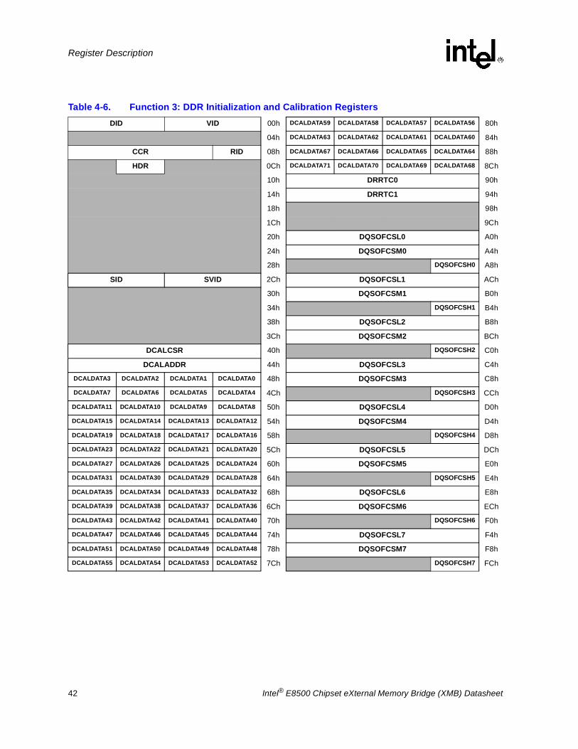
42 Intel® E8500 Chipset eXternal Memory Bridge (XMB) Datasheet
Register Description
Table 4-6. Function 3: DDR Initialization and Calibration RegistersDID VID 00h DCALDATA59 DCALDATA58 DCALDATA57 DCALDATA56 80h
04h DCALDATA63 DCALDATA62 DCALDATA61 DCALDATA60 84h
CCR RID 08h DCALDATA67 DCALDATA66 DCALDATA65 DCALDATA64 88h
HDR 0Ch DCALDATA71 DCALDATA70 DCALDATA69 DCALDATA68 8Ch
10h DRRTC0 90h
14h DRRTC1 94h
18h 98h
1Ch 9Ch
20h DQSOFCSL0 A0h
24h DQSOFCSM0 A4h
28h DQSOFCSH0 A8h
SID SVID 2Ch DQSOFCSL1 ACh
30h DQSOFCSM1 B0h
34h DQSOFCSH1 B4h
38h DQSOFCSL2 B8h
3Ch DQSOFCSM2 BCh
DCALCSR 40h DQSOFCSH2 C0h
DCALADDR 44h DQSOFCSL3 C4h
DCALDATA3 DCALDATA2 DCALDATA1 DCALDATA0 48h DQSOFCSM3 C8h
DCALDATA7 DCALDATA6 DCALDATA5 DCALDATA4 4Ch DQSOFCSH3 CCh
DCALDATA11 DCALDATA10 DCALDATA9 DCALDATA8 50h DQSOFCSL4 D0h
DCALDATA15 DCALDATA14 DCALDATA13 DCALDATA12 54h DQSOFCSM4 D4h
DCALDATA19 DCALDATA18 DCALDATA17 DCALDATA16 58h DQSOFCSH4 D8h
DCALDATA23 DCALDATA22 DCALDATA21 DCALDATA20 5Ch DQSOFCSL5 DCh
DCALDATA27 DCALDATA26 DCALDATA25 DCALDATA24 60h DQSOFCSM5 E0h
DCALDATA31 DCALDATA30 DCALDATA29 DCALDATA28 64h DQSOFCSH5 E4h
DCALDATA35 DCALDATA34 DCALDATA33 DCALDATA32 68h DQSOFCSL6 E8h
DCALDATA39 DCALDATA38 DCALDATA37 DCALDATA36 6Ch DQSOFCSM6 ECh
DCALDATA43 DCALDATA42 DCALDATA41 DCALDATA40 70h DQSOFCSH6 F0h
DCALDATA47 DCALDATA46 DCALDATA45 DCALDATA44 74h DQSOFCSL7 F4h
DCALDATA51 DCALDATA50 DCALDATA49 DCALDATA48 78h DQSOFCSM7 F8h
DCALDATA55 DCALDATA54 DCALDATA53 DCALDATA52 7Ch DQSOFCSH7 FCh
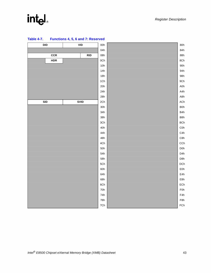
Intel® E8500 Chipset eXternal Memory Bridge (XMB) Datasheet 43
Register Description
Table 4-7. Functions 4, 5, 6 and 7: ReservedDID VID 00h 80h
04h 84h
CCR RID 08h 88h
HDR 0Ch 8Ch
10h 90h
14h 94h
18h 98h
1Ch 9Ch
20h A0h
24h A4h
28h A8h
SID SVID 2Ch ACh
30h B0h
34h B4h
38h B8h
3Ch BCh
40h C0h
44h C4h
48h C8h
4Ch CCh
50h D0h
54h D4h
58h D8h
5Ch DCh
60h E0h
64h E4h
68h E8h
6Ch ECh
70h F0h
74h F4h
78h F8h
7Ch FCh

44 Intel® E8500 Chipset eXternal Memory Bridge (XMB) Datasheet
Register Description
4.3 PCI Function 0 - Identification Registers
4.3.1 VID: Vendor Identification Register (F0)This register identifies Intel as the manufacturer of the XMB. Writes to this register have no effect.
4.3.2 DID: Device Identification Register (F0)This register combined with the Vendor Identification register uniquely identifies the XMB. Writes to this register have no effect.
4.3.3 RID: Revision Identification Register (F0)This register contains the revision number of the XMB.
Device: NodeIDFunction: 0Offset: 00-01h
Bit Attr Default Description
15:0 RO 8086h Vendor Identification NumberThe value assigned to Intel.
Device: NodeIDFunction: 0Offset: 02-03h
Bit Attr Default Description
15:0 RO 2600h Device Identification Number Identifies each function of the XMB
Device: NodeIDFunction: 0Offset: 08h
Bit Attr Default Description
7:0 RO 11hRevision Identification Number.“11h” = B1 stepping

Intel® E8500 Chipset eXternal Memory Bridge (XMB) Datasheet 45
Register Description
4.3.4 CCR: Class Code Register (F0)This register contains the Class Code for the XMB, specifying the device function.
4.3.5 HDR: Header Type Register (F0)This register identifies the header layout of the configuration space.
4.3.6 SVID: Subsystem Vendor Identification Register (F0)This register identifies the manufacturer of the system. This 16-bit register combined with the Device Identification Register uniquely identify any PCI device.
Device: NodeIDFunction: 0Offset: 09-0Bh
Bit Attr Default Description
23:16 RO 05hBase ClassThis field indicates the general device category. For the XMB, this field is hardwired to 05h, indicating it is a “memory controller”.
15:8 RO 00hSub-ClassThis field qualifies the Base Class, providing a more detailed specification of the device function. For the XMB, this field is hardwired to 00h, indicating it is a “RAM”.
7:0 RO 00h
Register-Level Programming InterfaceThis field identifies a specific programming interface (if any), that device independent software can use to interact with the device. There is no such interface defined for “memory controllers”.
Device: NodeIDFunction: 0Offset: 0E-0Fh
Bit Attr Default Description
7 RO 1b
Multi-function DeviceSelects whether this is a multi-function device, that may have alternative configuration layouts. The XMB has more than the 256 bytes of configuration registers allotted to a single function. Therefore, the XMB is defined to be a multifunction device, and this bit is hardwired to 1b.
6:0 RO All 0sConfiguration LayoutThis field identifies the format of the 10h through 3Fh space. The XMB uses header type “00”, and these bits are hardwired to 00h.
Device: NodeIDFunction: 0Offset: 2C-2Dh
Bit Attr Default Description
15:0 RWO 8086hVendor Identification NumberThe default value specifies Intel’s vendor ID. Each byte of this register will be writeable once. Second and successive writes to a byte will have no effect.

46 Intel® E8500 Chipset eXternal Memory Bridge (XMB) Datasheet
Register Description
4.3.7 SID: Subsystem Identity (F0)This register identifies the system.
4.4 PCI Function 1 Registers
4.4.1 VID: Vendor Identification Register (F1)This register identifies Intel as the manufacturer of the XMB. Writes to this register have no effect.
4.4.2 DID: Device Identification Register (F1)This register combined with the Vendor Identification register uniquely identifies the XMB. Writes to this register have no effect.
Device: Node_IDFunction: 0Offset: 2E-2Fh
Bit Attr Default Description
15:0 RWO 8086h Subsystem Identification NumberThe default value specifies Intel’s vendor ID. Each byte of this register will be writeable once. Second and successive writes to a byte will have no effect.
Device: NodeIDFunction: 1Offset: 00-01h
Bit Attr Default Description
15:0 RO 8086h Vendor Identification NumberThe value assigned to Intel.
Device: NodeIDFunction: 1Offset: 02-03h
Bit Attr Default Description
15:0 RO 2621h Device Identification NumberIdentifies each function of the XMB.

Intel® E8500 Chipset eXternal Memory Bridge (XMB) Datasheet 47
Register Description
4.4.3 RID: Revision Identification Register (F1)This register contains the revision number of the XMB.
4.4.4 CCR: Class Code Register (F1)This register contains the Class Code for the XMB, specifying the device function.
Device: NodeIDFunction: 1Offset: 08h
Bit Attr Default Description
7:0 RO 11hRevision Identification Number.“11h” = B1 stepping
Device: NodeIDFunction: 1Offset: 09-0Bh
Bit Attr Default Description
23:16 RO 05hBase ClassThis field indicates the general device category. For the XMB, this field is hardwired to 05h, indicating it is a “memory controller”.
15:8 RO 00hSub-ClassThis field qualifies the Base Class, providing a more detailed specification of the device function. For the XMB, this field is hardwired to 00h, indicating it is a “RAM”.
7:0 RO 00h
Register-Level Programming InterfaceThis field identifies a specific programming interface (if any), that device independent software can use to interact with the device. There is no such interface defined for “memory controllers”.

48 Intel® E8500 Chipset eXternal Memory Bridge (XMB) Datasheet
Register Description
4.4.5 HDR: Header Type Register (F1)This register identifies the header layout of the configuration space.
4.4.6 SVID: Subsystem Vendor Identification Register (F1)This register identifies the manufacturer of the system. This 16-bit register combined with the Device Identification Register uniquely identify any PCI device.
4.4.7 SID: Subsystem Identity (F1)This register identifies the system.
Device: NodeIDFunction: 1Offset: 0E-0Fh
Bit Attr Default Description
7 RO 1b
Multi-function DeviceSelects whether this is a multi-function device, that may have alternative configuration layouts. The XMB has more than the 256 bytes of configuration registers allotted to a single function. Therefore, the XMB is defined to be a multifunction device, and this bit is hardwired to 1b.
6:0 RO 00hConfiguration LayoutThis field identifies the format of the 10h through 3Fh space. The XMB uses header type “00”, and these bits are hardwired to 00h.
Device: NodeIDFunction: 1Offset: 2C-2Dh
Bit Attr Default Description
15:0 RWO 8086hVendor Identification NumberThe default value specifies Intel’s vendor ID. Each byte of this register will be writeable once. Second and successive writes to a byte will have no effect.
Device: Node_IDFunction: 1Offset: 2E-2Fh
Bit Attr Default Description
15:0 RWO 8086h Subsystem Identification Number The default value specifies Intel’s vendor ID. Each byte of this register will be writeable once. Second and successive writes to a byte will have no effect.

Intel® E8500 Chipset eXternal Memory Bridge (XMB) Datasheet 49
Register Description
4.4.8 IMILINE: IMI Cache Line Size (F1)This register reports the XMB’s cache line size. The XMB will return reads according to the value in LINE. If the XMB receives a legal LINE, it will acknowledge the “init” write to configuration address 00h, clear the RESPONSE bit, and update the LINE. If the XMB receives an illegal LINE, it will abort the “init” write, set the RESPONSE bit, and retain the previous LINE. IMI Chunk Size.
Device: NodeIDFunction: 1Offset: 40h
Bit Attr Default Description
7 RV 0b Reserved
6 RO 0b RESPONSE
5:0 RRW 00h LINE: Legal Cache line size
Encoding Description
0b Most recent update was an legal init write. Using most recent update.
1 Most recent update was an illegal init write. Retaining previous value.
Encoding Description
0b Specifies 64B
Other values Reserved
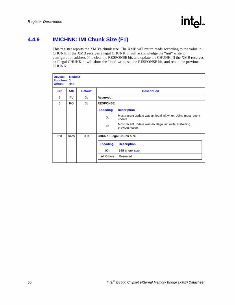
50 Intel® E8500 Chipset eXternal Memory Bridge (XMB) Datasheet
Register Description
4.4.9 IMICHNK: IMI Chunk Size (F1)This register reports the XMB’s chunk size. The XMB will return reads according to the value in CHUNK. If the XMB receives a legal CHUNK, it will acknowledge the “init” write to configuration address 04h, clear the RESPONSE bit, and update the CHUNK. If the XMB receives an illegal CHUNK, it will abort the “init” write, set the RESPONSE bit, and retain the previous CHUNK.
Device: NodeIDFunction: 1Offset: 44h
Bit Attr Default Description
7 RV 0b Reserved
6 RO 0b RESPONSE:
5:0 RRW 00h CHUNK: Legal Chunk size
Encoding Description
0b Most recent update was an legal init write. Using most recent update.
1b Most recent update was an illegal init write. Retaining previous value.
Encoding Description
00h 16B chunk size.
All Others Reserved

Intel® E8500 Chipset eXternal Memory Bridge (XMB) Datasheet 51
Register Description
4.4.10 IMICODE: IMI ECC Code Size (F1)This register reports the XMB’s ECC code. The XMB will return reads according to the value in CODE. If the XMB receives a legal CODE, it will acknowledge the “init” write to configuration address 08h, clear the RESPONSE bit, and update the CODE. If the XMB receives an illegal CODE, it will abort the “init” write, set the RESPONSE bit, and retain the previous CODE.
Device: NodeIDFunction: 1Offset: 48h
Bit Attr Default Description
7 RV 0b Reserved
6 RO 0b RESPONSE:
5:0 RRW 00h CODE: Legal Error Correction Code
Encoding Description
0b Most recent update was an legal init write. Using most recent update.
1 Most recent update was an illegal init write. Retaining previous value.
Encoding Description
03h This encoding specifies x8 SDDCAll Others Reserved

52 Intel® E8500 Chipset eXternal Memory Bridge (XMB) Datasheet
Register Description
4.4.11 IMIOFF: IMI Read Return Offset (F1)This register reports the XMB’s read return offset. The XMB returns reads according to the value in OFFSET. When the XMB receives a legal OFFSET, it acknowledges the “init” write to configuration address 0Ch, clears the RESPONSE bit, and updates the OFFSET. When the XMB receives an illegal OFFSET, it aborts the “init” write, sets the RESPONSE bit, and retains the previous OFFSET.
Device: NodeIDFunction: 1Offset: 4Ch
Bit Attr Default Description
7 RV 0b Reserved
6 RO 0b RESPONSE:
5:0 RRW 02h OFFSET: Legal Read Return offset
Encoding Description
0b Most recent update was an legal init write. Using most recent update.
1b Most recent update was an illegal init write. Retaining previous value.
Encoding Description
02h 2 packet delay. Only for configuration register accesses.XXh XX packet delay. Available for all access types.

Intel® E8500 Chipset eXternal Memory Bridge (XMB) Datasheet 53
Register Description
4.4.12 IMIAPR: IMI Read Return Aperture (F1)This register reports the XMB’s read return aperture. The XMB will return reads according to the value in APERTURE. If the XMB receives a legal APERTURE, it will acknowledge the “init” write to configuration address 10h, clear the RESPONSE bit, and update the APERTURE. If the XMB receives an illegal APERTURE, it will abort the “init” write, set the RESPONSE bit, and retain the previous APERTURE.
4.4.13 DDRFRQ: DDR Frequency (F1)This register defines the core and DDR frequencies and is based.
Device: NodeIDFunction: 1Offset: 50h
Bit Attr Default Description
7 RV 0b Reserved
6 RO 0b RESPONSE:
5:0 RRW 03h APERTURE: Legal Read Return Aperture
Encoding Description
0b Most recent update was an legal init write. Using most recent update.
1b Most recent update was an illegal init write. Retaining previous value.
Device: NodeIDFunction: 1Offset: 54h
Bit Attr Default Description
7:4 RV 0h Reserved
3:2 RO 0b NOW: DDR Frequency now.
1:0 RWLSX 0b NEXT: DDR Frequency after next reset
Encoding Core DDRCMD DDRDATA Technology
00b 266 MHz 133 MHz 266 MHz DDR 26601b 166 MHz 166 MHz 333 MHz DDR 333
10b 200 MHz 200 MHz 400 MHz DDR2 40011b Reserved
Encoding Core DDRCMD DDRDATA Technology
00b 266 MHz 133 MHz 266 MHz DDR 26601b 166 MHz 166 MHz 333 MHz DDR 33310b 200 MHz 200 MHz 400 MHz DDR2 40011b Reserved

54 Intel® E8500 Chipset eXternal Memory Bridge (XMB) Datasheet
Register Description
4.4.14 SPAD: Scratch Pad (F1)These bits have no effect upon the operation of the XMB. They are intended to be used by software for tracking changes in XMB state.
4.4.15 MTSTAT: Memory Test Status (F1)This register reflects the results of a fast verify.
Device: NodeIDFunction: 1Offset: 58-5Bh
Bit Attr Default Description
31:8 RW 000000hFREE:These bits are available for software definition.
7:0 RW 00hBADRANK: These bits are devoted to marking failed DIMM rank(s).
Device: NodeIDFunction: 1Offset: 5Dh
Bit Attr Default Description
7:2 RV All 0s Reserved
1 RWC 0b
CHANNEL1: DIMM on Channel 1 is badResult of running Fast Verify Mode in the XMBCFGNS register.
0 RWC 0b CHANNEL0: DIMM on Channel 0 is badResult of running Fast Verify Mode in the XMBCFGNS register.
Encoding Description
0b Good DIMM
1b Bad DIMM
Encoding Description
0b Good DIMM1b Bad DIMM

Intel® E8500 Chipset eXternal Memory Bridge (XMB) Datasheet 55
Register Description
4.4.16 XMBCFGNS: Memory Test and Scrub Register (F1) This register is used to control an engine that initializes, tests, and corrects errors in memory. Section 6.6.2.1, “Scrubbing” on page 6-137 describes scrub and Section 6.2.5, “Memory Test and Initialization” on page 6-120 describes test.
Device: NodeIDFunction: 1Offset: 5E-5Fh
Bit Attr Default Description
15:6 RV 00h Reserved
5:4 RW 00b
MTPAT: Memory Test Data Pattern Select This bit selects the data pattern for the Fast Write and Fast Verify modes (see definition for bits 2:1 in this register). The data pattern is propagated to the entire line as described in Section 6.2.5, “Memory Test and Initialization” on page 6-120.
3 RWC 0b
SCRBDONE: Scrub Complete The scrub unit will set this bit to 1 when it has completed scrubbing the selected memory segment and flushed scrub writes. The software should poll this bit after setting the Scrub Enable bit to determine when the selected operation has completed. Note: this bit is set each time the scrub unit completes a cycle though the selected memory segment. This bit is cleared by writing a '1'.
2:1 RW 00b
SCRBMODE: Scrub Mode Select These two bits determine the mode of operation that the scrubber unit is to run when Scrub Enable (bit 0) is set.
0 RW 0b
SCRBEN: Not preserved by SAVCFG. Scrub Enable. When set, this bit enables the scrubber to operate in the mode selected in bits 2:1 of this register. This bit must be cleared before enabling another Fast Write or Fast Verify operation.Clearing this bit resets the patrol scrub counters. This value is not preserved by SAVCFG.
Encoding Description
00b Zeros01b Random
10b Inverted random11b Reserved
Encoding Description
00b
Fast Write Mode - the XMB writes the data pattern selected in bits 4 and 5 of this register, at the fastest possible rate, walking randomly though the rank defined by the TEST_RANK field of Section 4.4.15, “MTSTAT: Memory Test Status (F1)” on page 4-54and then stopping.
01b Reserved.
10bPeriodic Scrub Mode - the XMB repeatedly walks though all memory defined by the MTR, where patrol scrubs occur every 16k core cycles.
11b
Fast Verify Mode - the XMB performs reads at the fastest possible rate, using the data value specified in bits 4:5 of this register, walking randomly though the rank defined by the TEST_RANK field of Section 4.4.15, “MTSTAT: Memory Test Status (F1)” on page 4-54, and then stopping.

56 Intel® E8500 Chipset eXternal Memory Bridge (XMB) Datasheet
Register Description
4.4.17 MC: Memory Control Settings (F1)Miscellaneous controls not implemented in other registers.
Device: NodeIDFunction: 1Offset: 60-63h
Bit Attr Default Description
31:23 RV 000h Reserved
22 RWC 0bWRTHROT: Write was throttledA write was either electrically or thermally throttled.
21 RWC 0bRDTHROT: Read was throttledA read was either electrically or thermally throttled.
20 RW 0b
ETHROT: 8-bank DIMM Electrical Throttling ModeAs enabled by MTR.THROTTLE:
See Table 6-9 “8-Bank DIMM Electrical Throttle Policy” on page 6-126.
19:16 RW 0h
SETH: Spare Error ThresholdA spare fail-over operation will commence when the DRC.SPAREN bit is set and a UERRCNT.RANK[i] and/or CERRCNT.RANK[i] count for one and only one rank hits this threshold.
15 RV 0bDDR1MODE: DDR1 ModeDDR technology is DDR1, Overrides default technology assumption in DDRFRQ.
14 RW 0b DEMSEN: Demand Scrub EnableEnables demand scrubbing.
13 RW 0b
SCRBALGO: Demand Scrub Algorithm
12 RW 0b
PSCRBALGO: Patrol Scrub Algorithm.
11 RW 0b
SSCRBALGO: Sparing Algorithm
10:9 RV 0h Reserved
Encoding Description
0b Aggressive Policy - 4 activates per 10 DDR_CLK’s1b Conservative Policy (more throttling) 4 activates per Trc
Encoding Description
0b Single device failure scrubbing algorithm1b Multiple device failure scrubbing algorithm
Encoding Description
0b Single device failure scrubbing algorithm
1b Multiple device failure scrubbing algorithm
Encoding Description
0b Single device failure scrubbing algorithm1b Multiple device failure scrubbing algorithm

Intel® E8500 Chipset eXternal Memory Bridge (XMB) Datasheet 57
Register Description
4.4.18 MS: Memory Status (F1)Miscellaneous status not reflected in other registers.
8 RW 0b
ISOLATE_DIMM: DIMM Isolation Mode.
7 RW 0b
THERMCAPEnables DDR thermal throttling. Limits DDR1 to 50% of full B/W, DDR2 to 62.5% full B/W, over a 100us period. See the NOW field in Section 4.4.43, “ERRPER: Error Period (F1)” .
6 RW 0b
WIPEWrites zeros to the failing DIMM during the sparing copy operation. Enabled by the “Spare Control Enable” bit in Section 4.4.23, “DRC: DRAM Controller Mode Register (F1)” .
5:3 RW 000b
SPRANKSpare rank. Target of the spare copy operation. This rank should not initially appear in a DMIR.RANK field. After the spare copy, the XMB will update the failed DMIR.RANK fields with this value. Enabled by the “Spare Control Enable” bit in Section 4.4.23, “DRC: DRAM Controller Mode Register (F1)” . Changes to this register will not be acknowledged by the hardware during a spare copy or wipe operation.
2:0 RW 000bTEST_RANKSelects the rank to be tested. Operates in conjunction with Section 4.4.16, “XMBCFGNS: Memory Test and Scrub Register (F1)” .
Device: NodeIDFunction: 1Offset: 60-63h
Bit Attr Default Description
Encoding Description
0bFast Write and Fast Verify scrub modes defined by the XMBCFGNS configuration register operate normally: over the entire rank.
1bFast Write and Fast Verify scrub modes defined by the XMBCFGNS configuration register generate a single access to the address stored in the RECMEM{A/B} configuration register.
Device: NodeIDFunction: 1Offset: 64-67h
Bit Attr Default Description
31:17 RV 0000h Reserved
16 RO 0b
LBTHR: Leaky Bucket Threshold Reached
15:11 RO 00h RQD: Read Queue DepthNumber of entries in the read queue.
Encoding Description
0b Leaky-bucket threshold not reached.
1bLeaky-bucket count matches MC.SETH. Generates an inband IMI “interrupt” signal. Cleared by reducing the offending count(s) in the UERRCNT/CERRCNT registers.

58 Intel® E8500 Chipset eXternal Memory Bridge (XMB) Datasheet
Register Description
10:6 RO 00hWQD: Write Queue DepthNumber of entries in the write post queue. When this is ‘0’, then the WP bit in this register is also ‘0’.
5 RO 0b
DSCIP: DIMM Sparing Copy In Progress0 - DIMM sparing copy not in progress.1 - DIMM sparing copy in progress. Set when DRC.SPAREN is set, and only one rank in UERRCNT/CERRCNT is at threshold. Remains set until SFO is set. Cleared when SFO is set.
4:2 RO 000bFR: Failed RankRank that was spared. Updated with the UERRCNT/FERRCNT rank that has reached threshold when DSCIP is set.
1 RO 0b
SFO: Spare Fail-Over
0 RO 0
WP: Writes Posted
Device: NodeIDFunction: 1Offset: 64-67h
Bit Attr Default Description
Encoding Description
0b Spare has not been substituted for failing DIMM rank.
1bSpare has been substituted for failing DIMM rank. Generates an inband IMI “Interrupt” signal. Cleared when DRC.SPAREN is cleared.
Encoding Description
0b All memory writes have been flushed. The WQD field in this register is “0”.
1b Memory writes are posted.

Intel® E8500 Chipset eXternal Memory Bridge (XMB) Datasheet 59
Register Description
4.4.19 IMIC: IMI Control (F1)This register reports XMB IMI status.
Device: NodeIDFunction: 1Offset: 68-6Bh
Bit Attr Default Description
31:26 RW 0Dh IMIPER:IMI Idle training periodThe IMI link requires periodic transitions to stay trained. IF IMIPER consecutive 16-bit windows occur on any of the 21 IMI outputs without the number of transitions specified by IMITRANS, the XMB will insert idle cycles in order to keep the link trained. There is a two-window latency before ideles are inserted. The default value of 13 (0Dh) insures that no more than 15 windows will occur between the idles.
25:22 RW 03h IMITRANS:Maximum Inbound Idle PeriodThis number of transitions must occur within a 16-bit window in order for an IMI output to stay trained. IF IMIPER consecutive 16-bit windows occur on any of the 21 IMI outputs without the number of transitions specified by IMITRANS, the XMB will insert idle cycles in order to keep the link trained.
21:16 RO 02h MOFFINIT:MOFF Initialization ValueThis field contains the value that the XMB will accept if written to the MOFF register. It is dependant on DDR type and ERRW value. The XMB will only accept this value if the MAPR register matches the value in MAPRINT.
15:14 RV 00h Reserved
13:8 RO 03hMAPRINT: MAPR Initialization ValueThis field contains the value that the XMB will accept if written to the MAPR register. It is dependent on DDR type and ERRW value.
7:4 RW 0BhWPQLLIM: Write Post Queue Lower LimitWhen the depth of the write post queue falls to WPQLLIM, the IMI releases stop-based flow control until the write post queue rises to WPQULIM.
3:0 RW Dh
WPQULIM: Write Post Queue Upper LimitWhen the depth of the write post queue rises to WPQULIM, the issue arbiter will hold pending IMI-initiated memory read requests until it issues a minimum of either four or WPQULIM writes to memory, and the IMI enforces stop-based flow control until the write post queue falls to WPQLLIM.

60 Intel® E8500 Chipset eXternal Memory Bridge (XMB) Datasheet
Register Description
4.4.20 IMIS: IMI Status (F1)This register reports XMB IMI status.
4.4.21 EMASK: Error Mask (F1)This register masks errors in the FERR and NERR registers. A ‘0’ in any field enables that error. A ‘1’ in any field masks (disables) that error. Multiple bits can be set in this register. An enabled error sets error status, updates error logs, and generates IMI signals. A masked error does not affect error status, error logs, or IMI signals.
Device: NodeIDFunction: 1Offset: 6Ch
Bit Attr Default Description
7:1 RV 00h Reserved
0 RO 0b LNKRDY: Link Ready
Encoding Description
0b IMI link is not ready.
1b IMI link is ready to accept requests and deliver responses.
Device: NodeIDFunction: 1Offset: 70h
Bit Attr Default Description
31:23 RV 00h Reserved
22 RW 1 X9: Fatal -- Write Post Buffer Parity Error
21 RW 1 X21: Fatal -- Detected Aliased Uncorrectable Errors
20 RW 1 IMI13: Uncorrectable -- Command Throttle Limit Exceeded
19 RW 1 X2: Uncorrectable -- Data ECC Error (Read)
18 RW 1 IMI1: Correctable -- Outbound CRC Error
17 RW 1 IMI5: Correctable -- Too Many Write Data packets
16 RW 1 IMI8: Correctable -- Unimplemented Command
15 RW 1 IMI9: Correctable -- Too Few Write Data packets
14 RW 1 IMI10: Correctable -- Memory Write Data Poisoned
13 RW 1 IMI12: Correctable -- Read Request Overflow
12 RW 0 IMI14: Correctable -- Rejected IMI write to “RRW” attributed registers
11 RW 1 IMI18: Correctable -- Configuration Write Data Poisoned
10 RW 1 X1: Correctable -- Data ECC Error (Request)
9 RW 1 X3: Correctable -- Patrol Scrub Error
8 RW 1 X4: UnCorrectable -- Data ECC Error (Patrol Scrub)
7 RW 1 X8: Correctable -- SPD Error (protocol)
6 RW 1 X10: Correctable -- Poisoned Data During DIMM Sparing Function

Intel® E8500 Chipset eXternal Memory Bridge (XMB) Datasheet 61
Register Description
4.4.22 DRT: DRAM Timing Register (F1)This register defines timing parameters that work with all DDR SDRAM’s in the memory subsystem. The parameters for these devices can be obtained by serial presence detect (see Section 6.4, “SMBus Port Description” on page 6-127). This register must be set to provide timings that satisfy the specifications of all SDRAM’s detected. If SDRAM’s present have different Tca’s, the maximum should be used to program this register. Consult the JEDEC DDR and DDR2 SDRAM specifications [7] [8] for the technology of the devices in use. An “DDR_CLK” is a command cycle, which is half the DDR rate.
5 RW 1 X11: Correctable -- Correctable Data Error during DIMM Sparing
4 RW 1 X12: Correctable -- Out-of-range Access (Read/Write)
3 RW 1 X13: Correctable -- Write Buffer Overflow
2 RW 1 X16: Correctable -- Memory Test Mismatch
1 RW 1 X17: Correctable -- More Than One IMI Config Command In Progress
0 RW 1 X22: Correctable -- Memory Request during Memory Test
Device: NodeIDFunction: 1Offset: 70h
Device: NodeIDFunction: 1Offset: 78-7Bh
Bit Attr Default Description
31 RV 0b Reserved
30 RW 0b TACA: Turn Around Cycle Add When set to 1, reads from DIMM3 to DIMM0 add an additional turn around cycle to avoid collisions.
29:28 RW 00b
B2BWR: Back To Back Write-Read Turn Around This field determines the minimum number of DDR_CLK’s between Write-Read data bursts. It applies to WR-RD pairs to any destinations (in same or different rows). The purpose of these bits is to control the turnaround time on the DQ bus. A value of 1 results in no bubble on the data bus.
Number of DDR_CLK’s at Specified DDR Frequencies
Encoding 266 MHz 333 MHz 400 MHz
00b Reserved Reserved Reserved01b 1 clock 1 clock 1 clock10b 2 clocks 2 clocks 2 clocks
11b Reserved Reserved 3 clocks

62 Intel® E8500 Chipset eXternal Memory Bridge (XMB) Datasheet
Register Description
27:26 RW 00b
B2BRW: Back-To-Back Read-Write Turn Around This field determines the data bubble duration between Read-Write data bursts. It applies to RD-WR pairs to any destinations (in same or different rows). The purpose of these bits is to control the turnaround time on the DQ bus. A value of 1 results in no bubble on the data bus.
25:24 RW 00b
B2BR: Back To Back Read Turn Around This field determines the data bubble duration between two reads destined to different ranks. The purpose of these bits is to control the turnaround time on the DQ bus. A value of 1 results in no bubble on the data bus.
23:22 RW 00b
TRFC: Auto refresh Cycle Time The required tCK cycles between/after auto refresh cycles to any particular DIMM.
21:20 RW 00b
TRRD: Trrd Row Delay The required row delay period between 2 activate commands accessing the same rank of a DIMM in tCK cycles.
Device: NodeIDFunction: 1Offset: 78-7Bh
Bit Attr Default Description
Number of DDR_CLK’s at Specified DDR Frequencies
Encoding 266 MHz 333 MHz 400 MHz
00b Reserved Reserved Reserved
01b 1 clock 1 clock 1 clock10b 2 clocks 2 clocks 2 clocks11b Reserved Reserved 3 clocks
Number of DDR_CLK’s at Specified DDR Frequencies
Encoding 266 MHz 333 MHz 400 MHz
00b Reserved Reserved Reserved01b 1 clock 1 clock 1 clock
10b 2 clocks 2 clocks 2 clocks11b Reserved Reserved 3 clocks
Number of DDR_CLK’s at Specified DDR Frequencies
Encoding 266 MHz 333 MHz 400 MHz
00b Reserved Reserved 15 clocks01b Reserved Reserved 21 clocks
10b 10 clocks 13 clocks 26 clocks11b 16 clocks 20 clocks 40 clocks
Number of DDR_CLK’s at Specified DDR Frequencies
Encoding 266 MHz 333 MHz 400 MHz
00b 1 clocks 1 clocks 1 clocks01b 2 clocks 2 clocks 2 clocks
10b 3 clocks 3 clocks 3 clocks11b Reserved Reserved 4 clocks

Intel® E8500 Chipset eXternal Memory Bridge (XMB) Datasheet 63
Register Description
19:18 RW 00b
TWTR: Internal Write to Read Command Delay
17:16 RV 0h Reserved
15:14 RW 00b
TRASMIN: This field controls the number of DRAM clocks to enforce as the ras cycle time in tCK cycles (also referred to as Trc).
13:12 RW 00b
TDAL: Tdal Write with Autoprecharge Recovery Delay Autoprecharge write recovery time plus precharge time. (Twr+Trp).
11:10 RW 00b
TRCD: Trcd RAS# to CAS# delay This bits controls the number of clocks inserted between a row activate command and a read or write command to that row in tCK cycles.
Device: NodeIDFunction: 1Offset: 78-7Bh
Bit Attr Default Description
Number of DDR_CLK’s at Specified DDR Frequencies
Encoding 266 MHz 333 MHz 400 MHz
00b 1 clocks 1 clocks 2 clocks01b 2 clocks 2 clocks Reserved
10b 3 clocks 3 clocks Reserved11b Reserved Reserved Reserved
Number of DDR_CLK’s at Specified DDR Frequencies
Encoding 266 MHz 333 MHz 400 MHz
00b Reserved Reserved Reserved01b 8 clocks Reserved 12 clocks
10b 9 clocks 10 clocks 13 clocks11b Reserved Reserved Reserved
Number of DDR_CLK’s at Specified DDR Frequencies
Encoding 266 MHz 333 MHz 400 MHz
00b 4 clocks Reserved 6 clocks01b 5 clocks 6 clocks 7 clocks10b Reserved Reserved Reserved
11b Reserved Reserved Reserved
Number of DDR_CLK’s at Specified DDR Frequencies
Encoding 266 MHz 333 MHz 400 MHz
00b Reserved Reserved Reserved01b 2 clocks 3 clocks 3 clocks10b 3 clocks 5 clocks 4 clocks11b 4 clocks 6 clocks 5 clocks

64 Intel® E8500 Chipset eXternal Memory Bridge (XMB) Datasheet
Register Description
9:8 RW 00b
TRP: Trp DRAM RAS# Precharge This bit controls the number of clocks that are inserted between a row precharge command and an activate command to the same row in tCK cycles.
7:6 RV 0h Reserved
5:4 RW 01b
TRRL: Read Round-Trip Latency Memory Subsystem Read Latency minus CAS latency. Measured from rising DDR_CLK edge when READ is driven on bus to the final rising HCLKIN edge before data is captured by XMB.
3:2 RW 01b
CASDLY: CAS# Latency The number of clocks between the rising edge used by DRAM’s to sample the Read Command and the rising edge that is used by the DRAM to drive read data.
Device: NodeIDFunction: 1Offset: 78-7Bh
Bit Attr Default Description
Number of DDR_CLK’s at Specified DDR Frequencies
Encoding 266 MHz 333 MHz 400 MHz
00b Reserved Reserved Reserved01b 2 clocks 2 clocks Reserved10b 3 clocks 3 clocks 3 clocks11b Reserved Reserved 4 clocks
Number of DDR_CLK’s at Specified DDR Frequencies
Encoding 266 MHz 333 MHz 400 MHz
00b 2.5 clocks 2.0 clocks 3.0 clocks
01b 3.0 clocks 3.0 clocks 4.0 clocks10b 2.0 clocks 4.0 clocks 2.0 clocks11b 3.5 clocks 5.0 clocks 5.0 clocks
Number of DDR_CLK’s at Specified DDR Frequencies
Encoding 266 MHz 333 MHz 400 MHz
00b 2.0 clocks 2.0 clocks Reserved01b 2.5 clocks 2.5 clocks 3.0 clocks
10b Reserved Reserved 4.0 clocks11b Reserved Reserved Reserved

Intel® E8500 Chipset eXternal Memory Bridge (XMB) Datasheet 65
Register Description
4.4.23 DRC: DRAM Controller Mode Register (F1)This register controls the mode of the DRAM Controller. An “DDR_CLK” is a command cycle, which is half the DDR rate.
1:0 RW 00b
B2BW: Back To Back Write Turn Around This field determines the minimum number of DDR_CLK’s between Write data bursts. It applies to WR pairs to any destinations (in same or different rows). The purpose of these bits is to control the turnaround time on the DQ bus. A value of 1 results in no bubble on the data bus It is expected that this setting will only be used in DDR2 mode with ODT in the event that ODT selections must change between ranks. The “11” encoding for DDR266 and DDR333 also sets the turnaround to the same rank to 4 to enable support for devices without concurrent autoprecharge.
Device: NodeIDFunction: 1Offset: 78-7Bh
Bit Attr Default Description
Number of DDR_CLK’s at Specified DDR Frequencies
Encoding 266 MHz 333 MHz 400 MHz
00b 0 clocks 0 clocks 0 clocks01b 1 clocks 1 clocks 1 clocks10b 2 clocks 2 clocks 3 clocks11b 2,4 clocks 2,4 clocks 0 clocks
Device: NodeIDFunction: 1Offset: 7C-7Fh
Bit Attr Default Description
31:30 RV 00b Reserved
29 RW 0bINITDONE: Initialization Complete This scratch bit communicates software state from the XMB to BIOS. BIOS sets this bit to 1 after initialization of the DRAM memory array is complete. This bit has no effect on XMB operation.
28 RW 0b
CKEN: CKE Enable Not preserved by SAVCFG.
27 RWST 0b
SRDISABLE:Disable DRAM self-refresh entry. When set, this bit prevents the XMB from sending a self-refresh entry command to the DIMMs at RST#. Instead, the DIMMs will be put into a power down mode.
26 RW 0b
OVLAPEN: Overlap enable
Encoding Description
0b CKE de-asserted.1b CKE asserted.
Encoding Description
0b Inhibits overlapped scheduling of row/col tenures.
1b Allows overlapped scheduling of activates prior to completing the outstanding column command.

66 Intel® E8500 Chipset eXternal Memory Bridge (XMB) Datasheet
Register Description
25 RW
0b TRCDEN: TRCD Enable
24:15 RV 000h Reserved
14:13 RW 00b
ODTZ: On-Die Termination Strength
12 RV 0b Reserved
11 RW 0b
DIFFDQSEN: Differential DQS EnableWhen cleared, DQSN strobe complement outputs are tri-stated and DQS receiver inputs are connected to DQSP and Vref. WHen set, DQSN outputs are enabled and DQS receiver inputs are connected to DQSP and DQSN.
10:8 RW 000b
RMS: Refresh Mode Select. Not preserved by SAVCFG.This field determines whether refresh is enabled and, if so, at what rate refreshes will be executed. When a value of “000” is written, the refresh counter is cleared.
7 RW 0b
RWPRDIS: Read/Write pointer reset disableDisables the resetting of DDR cluster FIF read and write pointers during normal operation that occurs when a READ command finishes executing and no additional READ commands are in process.
6 RW 0bDHG: DQS output half gainWhen set to 1, the amplifier gain is cut in half to support differential strobes for DDR2.
5:4 RV 00b Reserved
Device: NodeIDFunction: 1Offset: 7C-7Fh
Bit Attr Default Description
Encoding Description
0b Allows adding 1 DDR_CLK to TRCD if the controller believes this will help bandwidth.
1b Inhibits adding 1 DDR_CLK to TRCD.
Encoding Description
00 Reserved
01 Reserved10b Reserved11b 75 Ohms
Encoding Description
000b Refresh disabled. 001b Refresh enabled. Refresh interval 15.6 usec.010b Refresh enabled. Refresh interval 7.8 usec.011b Refresh enabled. Refresh interval 64 usec.
100b
Refresh enabled. Refresh interval:DDRFRQ.NOW.DDR_CLK’s.00 728.10 1,09211 1,456
101b Reserved110b Reserved
111b Refresh enabled. Refresh interval 64 DDR_CLKs (fast refresh mode).

Intel® E8500 Chipset eXternal Memory Bridge (XMB) Datasheet 67
Register Description
4.4.24 SPD: Serial Presence Detect Status Register (F1)This register provides the interface to the SPD bus (SCL and SDA signals) that is used to access the Serial Presence Detect EEPROM that defines the technology, configuration, and speed of the DIMMs controlled by the XMB. See Section 6.4, “SMBus Port Description” on page 6-127.
3 RW 0b
SPAREN: Spare Control Enable. Not preserved by SAVCFG. This bit when ‘1’ enables sparing, or when ‘0’ disables sparing. The SPRANK and WIPE fields of Section 4.4.15, “MTSTAT: Memory Test Status (F1)” define other characteristics of the sparing operation.
2:0 RV 000b Reserved
Device: NodeIDFunction: 1Offset: 7C-7Fh
Bit Attr Default Description
Device: NodeIDFunction: 1Offset: 80-81h
Bit Attr Default Description
15 RO 0b
RDO: Read Data ValidThis bit is set by the XMB when the Data field of this register receives read datafrom the SPD EEPROM after successful completion of an SPDR command. It iscleared by the XMB when a subsequent SPDR command is issued.
14 RO 0bWOD: Write Operation DoneThis bit is set by the XNB when a SPDW command has been completed on theSPD bus. It is cleared by the XMB when a subsequent SPDW command is issued.
13 RO 0b
SBE: SPD Bus ErrorThis bit is set by the XMB if it initiates an SPD bus transaction that does notcomplete successfully. It is cleared by the XMB when an SPDR or SPDW commandis issued.
12 RO 0bBUSY: Busy state.This bit is set by the XMB while an SPD command is executing.
11:8 RV 0h Reserved
7:0 RO 00hDATA: DataHolds data read from SPDR commands. Refer to Section 6.5.1, “SPD Asynchronous Handshake” .

68 Intel® E8500 Chipset eXternal Memory Bridge (XMB) Datasheet
Register Description
4.4.25 SPDCMD: Serial Presence Detect Command Register (F1)A write to this register initiates a DIMM EEPROM access through the SPD bus. See Section 6.4, “SMBus Port Description” on page 6-127.
4.4.26 CBC: Chip Boot Configuration (F1)This register reports the XMB SMBus Address.
Device: NodeIDFunction: 1Offset: 84-87h
Bit Attr Default Description
31:28 RW 1010b
DTI: Device Type IdentifierThis field specifies the device type identifier. Only devices with this device-type will respond to commands. “1010” specifies EEPROM’s. “0110” specifies a write-protect operation for an EEPROM. Other identifiers can be specified to target non-EEPROM devices on the SPD bus.
27 RV 0b Reserved
26:24 RW 000bSA: Slave AddressThis field identifies the DIMM EEPROM to be accessed through the SPD register according to Table 6-11 “SPD Addressing” on page 6-134.
23:16 RW 00hBA: Byte AddressThis field identifies the byte address to be accessed through the SPD register.
15:8 RW 00hDATA: DataHolds data to be written by SPDW commands. Refer to Section 6.5.1, “SPD Asynchronous Handshake” .
7:4 RW 000bDIV: Clock DividerSets the SPD bus clock frequency from 100 KHz to 4.3 KHz. Refer to Table 6-12 “SPD.DIV Clock Divider Frequency Table” on page 6-135.
3:1 RV 000b Reserved
0 RW 0bCMD: CommandWriting a ‘0’ to this bit initiates an SPDR command. Writing a ‘1’ to this bit initiates an SPDW command.
Device: NodeIDFunction: 1Offset: 88h
Bit Attr Default Description
7 RV 0b Reserved
6:2 RO 00010b SMBADDR: SMBus Address bits [6:2]
1:0 ROxxb
SMBADDR: SMBus Address bits [1:0]Value sampled from pins SMBA1 and SMBA0 at assertion of PWRGOOD.

Intel® E8500 Chipset eXternal Memory Bridge (XMB) Datasheet 69
Register Description
4.4.27 REIMEMB: DIMM Address Error Isolation Information B of Memory (F1)This register sets the bank address for the DIMM Isolation feature. It is organized to allow software to read the RECMEMB register and write its contents here without modification.
4.4.28 GPO: General Purpose Outputs (F1)This register drives the GPO[9:0] signals. It also saves the input state of pins 8:7 at PWRGOOD.
Device: NodeIDFunction: 1Offset: 89h
Bit Attr Default Description
7:6 RV 00b Reserved
5:3 RW 000b Bank
2:0 RV 000b Reserved
Device: NodeIDFunction: 1Offset: 8A-8Bh
Bit Attr Default Description
15 ROSX 1b
DDR Board: Input from the GPO8 at PWRGOOD
14 ROSX 1b
DDR Freq: Input from the GPO7 at PWRGOOD
13:10 RV 0h Reserved
9:0 RW 000h GPO: General Purpose Outputs
Encoding Description
0b DDR2 Memory riser present1b DDR Memory riser present
Encoding Description
0b DDR 333 Memory riser present1b DDR 266 Memory riser present

70 Intel® E8500 Chipset eXternal Memory Bridge (XMB) Datasheet
Register Description
4.4.29 REIMEMA: DIMM Address Error Isolation Information A of Memory (F1)This register sets the bank address for the DIMM Isolation feature. It is organized to allow software to read the RECMEMB register and write its contents here without modification.
4.4.30 FERR: First Error (F1)Errors are classified into two basic types: non-recoverable (fatal), and recoverable (uncorrectable and correctable). First errors are flagged in the FERR register. Multiple bits can be set in this register.
Unmasked “Fatal” errors generate “Fatal error” in-band IMI messages. Unmasked “Uncorrectable” errors generate “Uncorrectable error” in-band IMI messages. Unmasked “Correctable” errors generate “Correctable error” in-band IMI messages.
Associated with some of the errors flagged in the FERR register are control and data logs. A recoverable error log is the set of log registers that is updated by a recoverable error. A non-recoverable error log is the set of log registers that is updated by a non-recoverable error. Some log registers are updated by both recoverable and non-recoverable errors. Error log registers are not reliable unless an error associated with the log is reported in FERR.
Once a non-recoverable first error has been flagged (and logged), the log registers for that error remain locked until either 1) that bit in the FERR is cleared, 2) a power-up reset, 3) a PWRGOOD reset, or 4) a re-synchronizing RST#. Once a recoverable first error has been flagged (and logged), the log registers for that error cannot be over-written by another recoverable error until 1) that bit in the FERR is cleared, 2) a power-up reset, 3) a PWRGOOD reset, or 4) a re-synchronizing RST#. A recoverable error log can be over-written at any time by a subsequent non-recoverable error.
If errors associated with the same log register are detected simultaneously, the error with the more significant bit is flagged in FERR, and the others are flagged in NERR. Once a log register is locked, any subsequent error associated with that log register must be flagged only in the NERR register.
The following algorithm must be employed to properly associate FERR errors to their respective logs:
1. Read FERR
2. Read the log registers associated with errors recorded in FERR.
3. Read FERR again.
4. If higher-priority errors appeared in FERR that were associated with the same log registers that were captured, then read those log registers again.
Device: NodeIDFunction: 1Offset: 8C-8Fh
Bit Attr Default Description
31:29 RV 000b Reserved
26:14 RW 0000h RA: Row Address
13:0 RW 0000h CA: Column Address

Intel® E8500 Chipset eXternal Memory Bridge (XMB) Datasheet 71
Register Description
See Table 6-15 “Errors Detected by the XMB” on page 6-142 for detailed descriptions of each error, the response, what is logged, and the name of the log register.
Device: NodeIDFunction: 1Offset: 90-93h
Bit Attr Default Description
31:23 RV 000h Reserved
29:23 RV 00h Reserved
22 RWCST 0X9: Fatal -- Write Post Buffer Parity ErrorUpdate RECMEM{A/B}. Previously Posted Write is corrupted by XMB. XMB Functionality has been compromised.
21 RWCST 0 X21: Fatal -- Detected Aliased Uncorrectable ErrorsUpdate RECMEM{A/B}. XMB Functionality has been compromised.
20 RWCST 0 IMI13: Uncorrectable -- Command Throttle Limit Exceeded
19 RWCST 0 X2: Uncorrectable -- Data ECC Error (Read)Update RECMEM{A/B}. Update REDMEM if SAVCFG.SECURITY cleared.
18 RWCST 0IMI1: Correctable -- Outbound CRC ErrorUpdate RECXMI{A/B/C}. XMB flushes any write packet currently in progress. XMB drops data packets and re-aligns on the next write header.
17 RWCST 0IMI5: Correctable -- Too Many Write Data packetsXMB flushes any write packet currently in progress, and re-aligns write capture on the next write header.
16 RWCST 0
IMI8: Correctable -- Unimplemented CommandUpdate RECXMI{A/B/C}. If the command is recognizable as a read or write (a partial write, for example), the XMB aborts the command. Otherwise, the XMB ignores the command.
15 RWCST 0IMI9: Correctable --Too Few Write Data packetsXMB flushes any write packet currently in progress. XMB throws away data packets, and re-aligns write capture on the next write header.
14 RWCST 0 IMI10: Correctable -- Memory Write Data PoisonedIMI “poison” bit set. XMB poisons data written to memory.
13 RWCST 0 IMI12: Correctable -- Read Request OverflowUpdate ADRMEM{A/B}. XMB drops the read.
12 RWCST 0IMI14: Correctable -- Rejected IMI write to “RRW” attributed registersAbort and drop write, set the RESPONSE bit in the IMI configuration register, and update RECXCFG.
11 RWCST 0IMI18: Correctable -- Configuration Write Data PoisonedIMI “poison” bit set. XMB drops and aborts configuration write. Update RECXCFG with the access that was dropped.
10 RWCST 0
X1: Correctable -- Data ECC Error (Request)Update RECMEM{A/B}. Update REDMEM if SAVCFG.SECURITY cleared. Re-read. If re-read reveals a correctable error, then fix. The method for determining correctability of the error varies with MC.SCRBALGO.
9 RWCST 0X3: Correctable -- Patrol Scrub ErrorUpdate RECMEM{A/B}. Update REDMEM if SAVCFG.SECURITY cleared. Re-read. If re-read reveals a correctable error, then fix.
8 RWCST 0
X4: UnCorrectable -- Data ECC Error (Patrol Scrub)Do not include poisoned data.Update RECMEM{A/B}. Update REDMEM if SAVCFG.SECURITY cleared. Re-read. If re-read reveals a correctable error, then fix.
7 RWCST 0 X8: Correctable -- SPD Error (protocol)

72 Intel® E8500 Chipset eXternal Memory Bridge (XMB) Datasheet
Register Description
4.4.31 NERR: Successive Error (F1)This register is used to report successive errors. More than two bits can be set in this register. This register has the same format as the FERR register. See Table 6-15 “Errors Detected by the XMB” on page 6-142.
Unmasked “Fatal” errors generate “Fatal error” in-band IMI messages. Unmasked “Uncorrectable” errors generate “Uncorrectable error” in-band IMI messages. Unmasked “Correctable” errors generate “Correctable error” in-band IMI messages.
A first error may also cause a successive error to be logged in the NERR.
6 RWCST 0X10: Correctable -- Poisoned Data During DIMM Sparing FunctionUpdate RECMEM{A/B}. During Sparing Copy, the engine had to poison a location in the spare DIMM.
5 RWCST 0X11: Correctable -- Correctable Data Error during DIMM SparingUpdate RECMEM{A/B}. During Sparing Copy, the engine had to correct data location in the spare DIMM.
4 RWCST 0 X12: Correctable -- Out-of-range Access (Read/Write)Update ADRMEM{A/B}. Abort and drop write data. Abort read.
3 RWCST 0 X13: Correctable -- Write Buffer OverflowUpdate ADRMEM{A/B}. Drop the write command and data.
2 RWCST 0 X16: Correctable -- Memory Test MismatchUpdate MTSTAT and MTERR[7:0]
1 RWCST 0
X17: Correctable -- More Than One IMI Config Command In ProgressUpdate RECXCFG with the access that was dropped. Drop the second (offending) access. SMBus and JTAG requests concurrent with an IMI request do not cause this error and are not dropped.
0 RWCST 0 X22: Correctable -- Memory Request during Memory TestUpdate RECXMI{A/B/C}. XMB drops memory request, and any write data.
Device: NodeIDFunction: 1Offset: 90-93h
Bit Attr Default Description
Device: NodeIDFunction: 1Offset: 94-97h
31:22 RV 000h Reserved
22 RWCST 0b
X9: Fatal -- Write Post Buffer Parity ErrorPreviously Posted Write is corrupted by XMB. XMB Functionality has been compromised.
21 RWCST 0b X21: Fatal -- Detected Aliased Uncorrectable Errors
XMB Functionality has been compromised.
20 RWCST 0 IMI13: Uncorrectable -- Command Throttle Limit Exceeded
19 RWCST 0b
X2: Uncorrectable -- Data ECC Error (Read)Do not include poisoned data.Update REDMEM.
18 RWCST 0b
IMI1: Correctable -- Outbound CRC ErrorXMB must flush any write packet currently in progress. XMB drops data packets and re-aligns on the next write header.

Intel® E8500 Chipset eXternal Memory Bridge (XMB) Datasheet 73
Register Description
17 RWCST 0b
IMI5: Correctable -- Too Many Write PacketsXMB must flush any write packet currently in progress. XMB throws away data packets and re-aligns write capture on the next write header.
16 RWCST 0b
IMI8: Correctable -- Unimplemented CommandXMB must flush any partial write packets currently in progress. XMB throws away data packets and re-aligns write capture on the next write.
15 RWCST 0b
IMI9: Correctable -- Too Few Write PacketsXMB must flush any write packet currently in progress. XMB throws away data packets and re-aligns write capture on the next write header.
14 RWCST 0b IMI10: Correctable -- Memory Write Data Poisoned
IMI “poison” bit set. XMB poisons data written to memory.
13 RWCST 0b
IMI12: Correctable -- Read Request OverflowInbound IMI “abort” bit set. XMB drops the read.Update NRECMEM{A/B}.
12 RWCST 0b
IMI14: Correctable -- Rejected IMI write to “RRW” attributed registersAbort and drop write, set the RESPONSE bit in the IMI configuration register, and update RECXCFG.
11 RWCST 0b IMI18: Correctable -- Configuration Write Data Poisoned
IMI “poison” bit set. XMB drops and nacks configuration write.
10 RWCST 0b
X1: Correctable -- Data ECC Error (Request)Re-read. If re-read reveals a correctable error, then fix. The method for determining correctability of the error varies with MC.SCRBALGO.
9 RWCST 0b X3: Correctable -- Patrol Scrub Error
Re-read. If re-read reveals a correctable error, then fix.
8 RWCST 0b
X4: Correctable -- Data ECC Error (Patrol Scrub)Do not include poisoned data.Re-read. If re-read reveals a correctable error, then fix.
7 RWCST 0b X8: Correctable -- SPD Error (protocol)
6 RWCST 0b X10: Correctable -- Poisoned Data During DIMM Sparing Function
During Sparing Copy, the engine had to poison a location in the spare DIMM.
5 RWCST 0b X11: Correctable -- Correctable Data Error during DIMM Sparing
During Sparing Copy, the engine had to correct data location in the spare DIMM.
4 RWCST 0b X12: Uncorrectable -- Out-of-range Access (Read/Write)
Nack and drop write data.
3 RWCST 0b X13: Correctable -- Write Buffer Overflow
Drop and nack the write.
2 RWCST 0b X16: Correctable -- Memory Test Mismatch
1 RWCST 0b
X17: Correctable -- More Than One IMI Config Command In ProgressDrop and nack the second (offending) access. SMBus and JTAG requests concurrent with an IMI request do not cause this error and are not dropped.
0 RWCST 0b X22: Correctable -- Memory Request during Memory Test
Nack and drop write data.
Device: NodeIDFunction: 1Offset: 94-97h

74 Intel® E8500 Chipset eXternal Memory Bridge (XMB) Datasheet
Register Description
4.4.32 RECMEMA: DIMM Address Error Control Information Aof Memory (F1)This register latches control information for the first non-fatal memory error detected by the XMB. See Table 6-15 “Errors Detected by the XMB” on page 6-142 for a listing of the errors that use this log. The address of the error can be inferred from the MIR, DMIR, and MTR register settings. The contents of this register are only valid when one of the errors that set this register is logged in the FERR register.
4.4.33 RECMEXMB: DIMM Address Error Control Information Bof Memory (F1)This register latches control information for the first non-fatal memory error detected by the XMB. See Table 6-15 “Errors Detected by the XMB” on page 6-142 for a listing of the errors that use this log. The address of the error can be inferred from the MIR, DMIR, and MTR register settings. The contents of this register are only valid when one of the errors that set this register is logged in the FERR register.
Device: NodeIDFunction: 1Offset: 98-9Bh
Bit Attr Default Description
31:29 RV 000b Reserved
28:14 ROST 0000h RA: Row Address
13:0 ROST 0000h CA: Column Address
Device: NodeIDFunction: 1Offset: 9Ch
Bit Attr Default Description
7 ROST 0bMIRMISS: “A” address did not map into a valid interleave range.
6 RV 0b Reserved
5:3 ROST 000b BANK:
2:0 ROST 000b RANK:

Intel® E8500 Chipset eXternal Memory Bridge (XMB) Datasheet 75
Register Description
4.4.34 REDMEM: Memory Read Data Error Log (F1)This register latches data information for the first memory read error detected by the XMB. See Table 6-15 “Errors Detected by the XMB” on page 6-142 for a listing of the errors that use this log. The contents of this register are only valid when a correctable memory read or scrub error is logged in the FERR. The contents of this register should not change until the bit is cleared from the FERR register.
The code used to protect memory is the x8 SDDC code described in a future revision of this document.
4.4.35 ADRMEMA: IMI Address Error Control Information A (F1)This register latches control information for the first incompletely-decoded memory address error detected by the XMB. See Table 6-15 “Errors Detected by the XMB” on page 6-142 for a listing of the errors that use this log. The contents of this register are only valid when one of the errors that set this register is logged in the FERR register.
Device: NodeIDFunction: 1Offset: 9D-9Fh
Bit Attr Default Description
23:16 ROST 00hBITSINERRA: This field contains the 1st symbols indicated by the LOCATOR and LINEPART. The upper four bits contain the 2nd burst, and the lower four bits contain the 1st burst.
15:8 ROST 00hBITSINERRB:This field contains the 2nd symbols indicated by the LOCATOR and LINEPART. The upper four bits contain the 2nd burst, and the lower four bits contain the 1st burst.
7 RV 0b Reserved
6 ROST 0b
LINEPART:
5 RV 0b Reserved
4:0 ROST 00h LOCATOR: This field indicates the physical x8 location (or adjacent x4 locations) in error. The encoding is 17 down to 0, with 17 down to 9 the physical locations of x8 parts on DIMM channel 1, and 8 down to 0 the physical locations of x8 parts on DIMM channel 0.
Encoding Bytes
0b [31:0]1b [63:32]
Device: NodeIDFunction: 1Offset: A0-A3h
Bit Attr Default Description
31:0 ROST All 0’s AL: “A” Address bits [37:6]Updated on MIR miss or write buffer overflow.

76 Intel® E8500 Chipset eXternal Memory Bridge (XMB) Datasheet
Register Description
4.4.36 ADRMEMB: IMI Address Error Control Information B (F1)This register latches control information for the first incompletely-decoded memory address error detected by the XMB. See Table 6-15 “Errors Detected by the XMB” on page 6-142 for a listing of the errors that use this log. The contents of this register are only valid when one of the errors that set this register is logged in the FERR register.
4.4.37 RECXCFG: Correctable or Uncorrectable Error ControlInformation of Configuration Register (F1)This register latches control information for the first non-fatal configuration error detected by the XMB. See Table 6-15 “Errors Detected by the XMB” on page 6-142 for a listing of the errors that use this log. The contents of this register are only valid when one of the errors that set this register is logged in the FERR register.
Device: NodeIDFunction: 1Offset: A4h
Bit Attr Default Description
7:4 RV 00h Reserved
3 ROST 0b SALIAS: “S” address exceeds physical rank size.
2 ROST 0b MIRMISS: “A” address exceeded MIR limits.Set on MIR miss.
1:0 ROST 00b AH: “A” Address bits [39:38]Updated on MIR miss or write buffer overflow.
Device: NodeIDFunction: 1Offset: AA-ABh
Bit Attr Default Description
15:13 RV 000b Reserved
12:10 ROST 000b FUNCTION:
9:8 ROST 00b SIZE:
7:0 ROST 0h REGISTER:
Encoding Description
00b 1 byte01b 2 byte10b 3 byte11b 4 byte
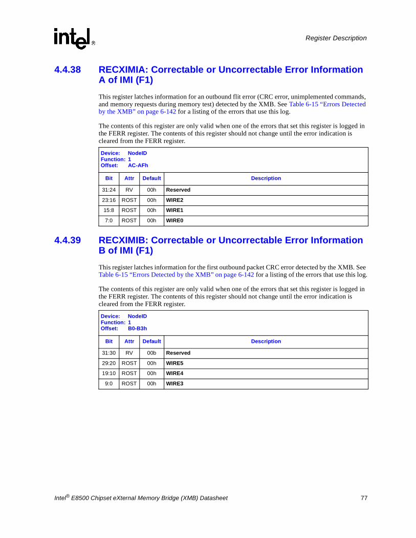
Intel® E8500 Chipset eXternal Memory Bridge (XMB) Datasheet 77
Register Description
4.4.38 RECXIMIA: Correctable or Uncorrectable Error InformationA of IMI (F1)This register latches information for an outbound flit error (CRC error, unimplemented commands, and memory requests during memory test) detected by the XMB. See Table 6-15 “Errors Detected by the XMB” on page 6-142 for a listing of the errors that use this log.
The contents of this register are only valid when one of the errors that set this register is logged in the FERR register. The contents of this register should not change until the error indication is cleared from the FERR register.
4.4.39 RECXIMIB: Correctable or Uncorrectable Error InformationB of IMI (F1)This register latches information for the first outbound packet CRC error detected by the XMB. See Table 6-15 “Errors Detected by the XMB” on page 6-142 for a listing of the errors that use this log.
The contents of this register are only valid when one of the errors that set this register is logged in the FERR register. The contents of this register should not change until the error indication is cleared from the FERR register.
Device: NodeIDFunction: 1Offset: AC-AFh
Bit Attr Default Description
31:24 RV 00h Reserved
23:16 ROST 00h WIRE2
15:8 ROST 00h WIRE1
7:0 ROST 00h WIRE0
Device: NodeIDFunction: 1Offset: B0-B3h
Bit Attr Default Description
31:30 RV 00b Reserved
29:20 ROST 00h WIRE5
19:10 ROST 00h WIRE4
9:0 ROST 00h WIRE3

78 Intel® E8500 Chipset eXternal Memory Bridge (XMB) Datasheet
Register Description
4.4.40 RECXIMIC: Correctable or Uncorrectable Error InformationC of eXternal Mem. Interface (F1)This register latches information for the first outbound packet CRC error detected by the XMB. See Table 6-15 “Errors Detected by the XMB” on page 6-142 for a listing of the errors that use this log.
The contents of this register are only valid when one of the errors that set this register is logged in the FERR register. The contents of this register should not change until the error indication is cleared from the FERR register.
4.4.41 UERRCNT: Uncorrectable Error Count (F1)This register implements the “leaky-bucket” counters for uncorrectable errors for each rank. Each field “limits” at a value of “15” (“1111”). Non-zero counts are decremented when the ERRPER threshold is reached by the error period counter. Counts start to increment only when MC.MSETH is set to a non-zero value. Counts are frozen at the threshold defined by MC.SETH and set the MS.LBTHR bit. Writing a value of “1111” clears and thaws the count. Changing MC.SETH has no effect upon a frozen count.
Device: NodeIDFunction: 1Offset: B4-B7h
Bit Attr Default Description
31:24 ROST 00h WIRE9
23:16 ROST 00h WIRE8
15:8 ROST 00h WIRE7
7:0 ROST 00h WIRE6
Device: NodeIDFunction: 1Offset: B8-BBh
Bit Attr Default Description
31:28 RWCST 0h RANK7: Error Count for Rank 7.
27:24 RWCST 0h RANK6: Error Count for Rank 6.
23:20 RWCST 0h RANK5: Error Count for Rank 5.
19:16 RWCST 0h RANK4: Error Count for Rank 4.
15:12 RWCST 0h RANK3: Error Count for Rank 3.
11:8 RWCST 0h RANK2: Error Count for Rank 2.
7:4 RWCST 0h RANK1: Error Count for Rank 1.
3:0 RWCST 0h RANK0: Error Count for Rank 0.

Intel® E8500 Chipset eXternal Memory Bridge (XMB) Datasheet 79
Register Description
4.4.42 CERRCNT: Correctable Error Count (F1)This register implements the “leaky-bucket” counters for correctable errors for each rank. Each field “limits” at a value of “15” (“1111”). Non-zero counts are decremented when the ERRPER threshold is reached by the error period counter. Counts start to increment only when MC.MSETH is set to a non-zero value. Counts are frozen at the threshold defined by MC.SETH and set the MS.LBTHR bit. Writing a value of “1111” clears and thaws the count. Changing MC.SETH has no effect upon a frozen count.
4.4.43 ERRPER: Error Period (F1)Non-zero UERRCNT and CERRCNT counts are decremented when the error period counter reaches this threshold. The error period counter is cleared on reset or when it reaches this threshold. The error period counter increments every 65,536 cycles. Table 4-8 indicates the timing characteristics of this register:
Device: NodeIDFunction: 1Offset: BC-BFh
Bit Attr Default Description
31:28 RWCST 0h RANK7: Error Count for Rank 7.
27:24 RWCST 0h RANK6: Error Count for Rank 6.
23:20 RWCST 0h RANK5: Error Count for Rank 5.
19:16 RWCST 0h RANK4: Error Count for Rank 4.
15:12 RWCST 0h RANK3: Error Count for Rank 3.
11:8 RWCST 0h RANK2: Error Count for Rank 2.
7:4 RWCST 0h RANK1: Error Count for Rank 1.
3:0 RWCST 0h RANK0: Error Count for Rank 0.
Table 4-8. Timing Characteristics of ERRPER
DDR Frequency Per Increment Maximum Period
DDR1 266MHz 245.76 µs 12 days, 5 hours, 12 minutes, 11.162 seconds
DDR1 333MHz 393.22 µs 19 days, 13 hours, 7 minutes, 29.859 seconds
DDR2 400MHz 327.68 µs 16 days, 6 hours, 56 minutes, 14.883 seconds
Device: NodeIDFunction: 1Offset: C0-C3h
Bit Attr Default Description
31:0 RW All 0s THRESH: UERRCNT / CERRCNT decrement threshold.

80 Intel® E8500 Chipset eXternal Memory Bridge (XMB) Datasheet
Register Description
4.4.44 BADRAMA: Bad DRAM Marker A (F1)This register implements “failed-device” markers for the enhanced demand scrub algorithm (MC.SCRBALGO = ‘1’). Hardware “marks” bad devices. The “mark” is a number between 1 and 18 inclusive. A value of “00000” indicates an “un-marked” rank: all RAM’s are presumed “good”. An adjacent pair of x4 DRAM’s is treated as a single x8 DRAM.
4.4.45 BADRAMB: Bad DRAM Marker B (F1)This register implements “failed-device” markers for the enhanced demand scrub algorithm (MC.SCRBALGO = ‘1’). Hardware “marks” bad devices. The “mark” is a number between 1 and 18 inclusive. A value of “00000” indicates an “un-marked” rank: all DRAM’s are presumed “good”. An adjacent pair of x4 DRAM’s is treated as a single x8 DRAM.
Device: NodeIDFunction: 1Offset: C4-C7h
Bit Attr Default Description
31:30 RV 00b Reserved
29:25 RWCST 00h RANK5: Bad device in Rank 5.
24:20 RWCST 00h RANK4: Bad device in Rank 4.
19:15 RWCST 00h RANK3: Bad device in Rank 3.
14:10 RWCST 00h RANK2: Bad device in Rank 2.
9:5 RWCST 00h RANK1: Bad device in Rank 1.
4:0 RWCST 00h RANK0: Bad device in Rank 0.
Device: NodeIDFunction: 1Offset: C8-CAh
Bit Attr Default Description
15:10 RV 00h Reserved
9:5 RWCST 00h RANK7: Bad device in Rank 7.
4:0 RWCST 00h RANK6: Bad device in Rank 6.

Intel® E8500 Chipset eXternal Memory Bridge (XMB) Datasheet 81
Register Description
4.4.46 RECWBUF[1:0]: Uncorrectable Error Information of Write Post Buffer 1/0 (F1)This register contains information logged by the XMB when a write post buffer parity error occurs. See Table 6-15 “Errors Detected by the XMB” on page 6-142 a listing of the errors that use this log.
The contents of this register are only valid when one of the errors that set this register is logged in the FERR register. The contents of this register should not change until the error indication is cleared from the FERR register.
4.4.47 TERR[7:0]: Memory Test Error Address and Data (F1)These eight 4-byte registers store the first 4 failing addresses found during memory test. 28 address bits are stored, including the bank, row, and column with the exception of the two column LSBs that define the chunk ordering of a burst on the data bus. The address is stored in a TBD format. In addition to the address, there is a fail status bit for each nibble of the data bus. The address and data format for the first failure stored in MTERR0/1 is shown in the table below. Subsequent errors are stored in the other registers in the same format.
Device: NodeIDFunction: 1Offset: D0-D3h, CC-CFh
Bit Attr Default Description
31:18 RV 0000h Reserved
17:6 ROST 000h PARSYND: Parity Syndrome.
5:1 ROST 00h RAMADDR: Buffer Entry Containing the Error.
0 ROST 0 HALF: Most Significant 72 Bits Contained the Error.
Device: NodeIDFunction: 1Offset: F0h, ECh, E8h, E4h, E0h, DCh, D8h, D4h
Bit Attr Default Description
31:0 RWC 0000h MTERRSee table below for format.

82 Intel® E8500 Chipset eXternal Memory Bridge (XMB) Datasheet
Register Description
Table 4-9. MTERR Address and Data FormatMTERR Address and Data format
Bit MTERR1 MTERR0
31
Address[27:0]Physical DRAM address
packed in {bank, col[msb:lsb+2], row} order.
Number of bits in bank, col, and row are defined
by MTR[3:0] csr
DDR_B_DQS15 Fail
30 DDR_B_DQS6 Fail
29 DDR_B_DQS14 Fail
28 DDR_B_DQS5 Fail
27 DDR_B_DQS13 Fail
26 DDR_B_DQS4 Fail
25 DDR_B_DQS12 Fail
24 DDR_B_DQS3 Fail
23 DDR_B_DQS11 Fail
22 DDR_B_DQS2 Fail
21 DDR_B_DQS10 Fail
20 DDR_B_DQS1 Fail
19 DDR_B_DQS9 Fail
18 DDR_B_DQS0 Fail
17 DDR_A_DQS17 Fail
16 DDR_A_DQS8 Fail
15 DDR_A_DQS16 Fail
14 DDR_A_DQS7 Fail
13 DDR_A_DQS15 Fail
12 DDR_A_DQS6 Fail
11 DDR_A_DQS14 Fail
10 DDR_A_DQS5 Fail
9 DDR_A_DQS13 Fail
8 DDR_A_DQS4 Fail
7 DDR_A_DQS12 Fail
6 DDR_A_DQS3 Fail
5 DDR_A_DQS11 Fail
4 DDR_A_DQS2 Fail
3 DDR_B_DQS17 Fail DDR_A_DQS10 Fail
2 DDR_B_DQS8 Fail DDR_A_DQS1 Fail
1 DDR_B_DQS16 Fail DDR_A_DQS9 Fail
0 DDR_B_DQS7 Fail DDR_A_DQS0 Fail

Intel® E8500 Chipset eXternal Memory Bridge (XMB) Datasheet 83
Register Description
4.4.48 CKDIS: DRAM CMDCLK Disable (F1)
4.4.49 DRAMISCTL: Miscellaneous DRAM DDR Cluster Control (F1)
Device: NodeIDFunction: 1Offset: F4h
Bit Attr Default Description
7:4 RWST Fh CKDIS: Disables DRAM CMDCLK/CMDCLK# pairs 3 to 0. These bits tri-state the clock pairs when set.
3:0 RWST Fh CKDISRST: Disables DRAM CMDCLK/CMDCLK# pairs 3 to 0 at MPRESET. These bits tri-state the clock pairs at MPRESET when set.
Device: NodeIDFunction: 1Offset: F8-FBh
Bit Attr Default Description
31:27 RW 09h DRVOVR: Enable drive override on all ddr drivers:
26 RW 0 Reserved
25 RV 0 Reserved
24 RW 0 Reserved
23 RW 0 Reserved
22 RW 0 Reserved
21 RW 0 SLVBYP: Sets all DLL delay elements to minimum values, bypasses DLL slave delays for strobe calibration
20 RV 0 Reserved
19:17 RW 000 CH0SLVLEN: Coarse control for ch0 DQS slave delays
16:14 RW 000 CH1SLVLEN: Coarse control for ch1 DQS slave delays
13:12 RW 00 MASTLEN: Coarse control for master DLLs
11:8 RW 0h MASTMIX: Fine control for master DLLs
7:4 RW 0h VREF: Vref selection
3:0 RV 0h Reserved
Encoding Description
1xnnnb Override compensation selecting nnn legs.
0nnnnbEnable compensation with impedance Rodt/(k/2), where Rodtis the resistance value between XMB pins DBDRVCRES and DBCRES0, and where k=0nnnn.

84 Intel® E8500 Chipset eXternal Memory Bridge (XMB) Datasheet
Register Description
4.4.50 DDR2ODTC: DDR-II DRAM On-Die Termination Control (F1)
4.5 PCI Function 2 - Memory Interleaving Registers
4.5.1 VID: Vendor Identification Register (F2)This register identifies Intel as the manufacturer of the XMB. Writes to this register have no effect.
4.5.2 DID: Device Identification Register (F2)This register combined with the Vendor Identification register uniquely identifies the XMB. Writes to this register have no effect.
Device: NodeIDFunction: 1Offset: FC-FFh
Bit Attr Default Description
31:28 RW 0h R3ODTWR: DODT[3:0] bus for write access with CS6 or CS1 asserted
27:24 RW 0h R3ODTRD: DODT[3:0] bus for read access with CS6 or CS1 asserted
23:20 RW 0h R2ODTWR: DODT[3:0] bus for write access with CS4 or CS3 asserted
19:16 RW 0h R2ODTRD: DODT[3:0] bus for read access with CS4 or CS3 asserted
15:12 RW 0h R1ODTWR: DODT[3:0] bus for write access with CS2
11:8 RW 0h R1ODTRD: DODT[3:0] bus for read access with CS2
7:4 RW 0h R0ODTWR: DODT[3:0] bus for write access with CS0
3:0 RW 0h R0ODTRD: DODT[3:0] bus for read access with CS0
Device: NodeIDFunction: 2Offset: 00-01h
Bit Attr Default Description
15:0 RO 8086h Vendor Identification NumberThe value assigned to Intel.
Device: NodeIDFunction: 2Offset: 02-03h
Bit Attr Default Description
15:0 RO 2622h Device Identification Number Identifies each function of the XMB

Intel® E8500 Chipset eXternal Memory Bridge (XMB) Datasheet 85
Register Description
4.5.3 RID: Revision Identification Register (F2)This register contains the revision number of the XMB.
4.5.4 CCR: Class Code Register (F2)This register contains the Class Code for the XMB, specifying the device function.
Device: NodeIDFunction: 2Offset: 08h
Bit Attr Default Description
7:0 RO 11h Revision Identification Number.“11h” = B1 stepping
Device: NodeIDFunction: 2Offset: 09-0Bh
Bit Attr Default Description
23:16 RO 05h Base Class.This field indicates the general device category. For the XMB, this field is hardwired to 05h, indicating it is a “memory controller”.
15:8 RO 00h Sub-Class.This field qualifies the Base Class, providing a more detailed specification of the device function. For the XMB, this field is hardwired to 00h, indicating it is a “RAM”.
7:0 RO 00h Register-Level Programming Interface.This field identifies a specific programming interface (if any), that device independent software can use to interact with the device. There is no such interface defined for “memory controllers”.

86 Intel® E8500 Chipset eXternal Memory Bridge (XMB) Datasheet
Register Description
4.5.5 HDR: Header Type Register (F2)This register identifies the header layout of the configuration space.
4.5.6 SVID: Subsystem Vendor Identification Register (F2)This register identifies the manufacturer of the system. This 16-bit register combined with the Device Identification Register uniquely identify any PCI device.
4.5.7 SID: Subsystem Identity (F2)This register identifies the system.
Device: NodeIDFunction: 2Offset: 0E-0Fh
Bit Attr Default Description
7 RO 1b Multi-function Device.Selects whether this is a multi-function device, that may have alternative configuration layouts. The XMB has more than the 256 bytes of configuration registers allotted to a single function. Therefore, the XMB is defined to be a multifunction device, and this bit is hardwired to 1b.
6:0 RO All 0s Configuration Layout.This field identifies the format of the 10h through 3Fh space. The XMB uses header type “00”, and these bits are hardwired to 00h.
Device: NodeIDFunction: 2Offset: 2C-2Dh
Bit Attr Default Description
15:0 RWO 8086h Vendor Identification Number.The default value specifies Intel’s vendor ID. Each byte of this register will be writeable once. Second and successive writes to a byte will have no effect.
Device: Node_IDFunction: 2Offset: 2E-2Fh
Bit Attr Default Description
15:0 RWO 8086h Subsystem Identification Number: The default value specifies Intel’s vendor ID. Each byte of this register will be writeable once. Second and successive writes to a byte will have no effect.

Intel® E8500 Chipset eXternal Memory Bridge (XMB) Datasheet 87
Register Description
4.5.8 SAVCFG: Configuration Protection (F2)This register controls resource maintenance and access.
4.5.9 Sticky RegistersIn general, registers are set to default values by resets. However, not all resets affect all registers in the same way. Some registers behave differently based on the value of the SAVCFG bit. The following table summarizes
In the descriptions above, a “maybe sticky” register is considered “not sticky” if SAVCFG is low and is considered “sticky” if SAVCFG is high.
Dev ice:NodeIDFunction: 2Offset: 60h
Bit Attr Default Description
7:3 RV 00h Reserved
2 RWST 0 CFGLOCK: Restrict Access to all registersWhen this bit is set, writes through JTAG or SMBus to all registers are inhibited.XMB ensures that an IMI command to set CFGLOCK takes effect before a subsequent JTAG or SMBus command has a chance to clear it.
1 RW 0 SAVCFG: Preserve ConfigurationWhen this bit is set, most configuration registers with a RW attribute are not defaulted by IMI reset. When this bit is set, the DDRFRQ register is locked; writes from any interface to DDRFRQ are inhibited. This bit is cleared by IMI reset. Therefore, software must set it after IMI reset if this behavior is desired for the next IMI reset.This bit is cleared when DDRFRQ.NEXT!= DDRFRQ.NOW.
0 RWST 0 SECURITY: Restrict Access to function 2 registersWhen this bit is set, writes through JTAG or SMBus to registers mapped to function 2 are inhibited.
Table 4-10. Register Types and Resets
RegisterType
For SAVCFG = 0Reset By
For SAVCFG = 1Reset By Examples
notsticky
Any IMI ResetPowerGood Reset
Most flip-flops which are not in configuration registers.RO fields in configuration registers.
RRW fields in configuration registers.
stickyIMI Resync ResetPowerGood Reset
*ST fields in configuration registers
maybesticky
Any IMI ResetPowerGood Reset
IMI Resync ResetPowerGood Reset
Most RW, RWC, RWS, RWL, and RWOfields in configuration registers.
extrasticky PowerGood Reset
Registers which run on XCLK.DDRFRQ.NEXT
JTAG Test Reset Registers which run on TCLK.

88 Intel® E8500 Chipset eXternal Memory Bridge (XMB) Datasheet
Register Description
4.5.10 TOLM: Top Of Low Memory (F2)This register defines the MMIO gap. See Section 4.5.11, “IMIR[5:0]: IMI Interleave Range (F2)” on page 4-88.
Whereas the MIR.LIMIT’s are adjustable, TOLM establishes a fixed limit at 4 GB.
4.5.11 IMIR[5:0]: IMI Interleave Range (F2)These registers define this XMB’s interleave participation in IMI space. See the MIR address translation algorithm in Section 6.2.8.5, “Address Translation” on page 6-122.
Each register defines a range. If the IMI (A) address falls in the range defined by an IMIR, the ways fields in that IMIR define the number and interleave position of this XMB’s IMI way participation. In 64B mode, the way-sensitive address bits are A[7:6]. In 128B mode, the way-sensitive address bits are A[8:7]. The way function for {1 way set, 2 cube-adjacent ways set, 2 cube-non-adjacent ways set, 4 ways set} is {“00”, “10”, “01”, “11”} respectively. Matching addresses participate in the corresponding ways. Enabling exactly 3 ways is illegal.
Compensation for a non-4GB MMIO gap size is performed by adjusting the limit of each range upward if it is above TOLM as shown in Table 4-11.
Device: NodeIDFunction: 2Offset: 6Ch
Bit Attr Default Description
15:12 RW 0h TOLMThis field corresponds to A[31:28]. 0 = 4 GB, “1111” = 3.75 GB, and so on down to “0001” corresponds to 0.25GB.
11:1 RV 000h Reserved
0 RW 0b ACHKSDIS:Alias Checks Disable. When this field is “1”, all memory aliasing checks are disabled.
Table 4-11. Interleaving of an Address is Governed by MIR[i] if
Limit above TOLM? Match MIR[i] if
MIR[i].LIMIT[3:0] <= TOLM[3:0] MIR[i].LIMIT[9:0] > A[37:28] >= MIR[i-1].LIMIT[9:0]
MIR[i].LIMIT[3:0] > TOLM[3:0] MIR[i].LIMIT[9:0] + 10H - TOLM[3:0] > A[37:28] >=max(MIR[i-1]a.LIMIT[9:0], 4GB)
NOTE:a. for MIR[0], MIR[i-1] is defined to be 0.

Intel® E8500 Chipset eXternal Memory Bridge (XMB) Datasheet 89
Register Description
4.5.12 MTR[3:0]: Memory Technology Registers (F2)These registers define the organization of the DIMMs. There is one MTR for each pair of slots comprising either one or two ranks. The parameters for these devices can be obtained by serial presence detect (see Section 6.4, “SMBus Port Description” on page 6-127).
Device: NodeIDFunction: 2Offset: 80-81h, 84-85h, 88-89h, 8C-8Fh, 90-91h, 94-95h
Bit Attr Default Description
15 RV 0 Reserved
14:4 RW 000h LIMITThis field defines the highest address in the range A[38:28] prior to modification by the TOLM register. (A[38] is ignored).
3 RW 0b WAY3Memory requests participate in this MIR range if this bit is set and (the bitwise AND (the way-sensitive address bits matched against “11”) OR with the way function) is ‘1’.
2 RW 0b WAY2Memory requests participate in this MIR range if this bit is set and (the bitwise “and” of (the way-sensitive address bits matched against “10”) “or”d with the way function) is ‘1’.
1 RW 0b WAY1Memory requests participate in this MIR range if this bit is set and ((the bitwise “and” of ((the way-sensitive address bits matched against “01”) “or”d with the way function) is ‘1’.
0 RW 0b WAY0Memory requests participate in this MIR range if this bit is set and (the bitwise “and” of (the way-sensitive address bits matched against “00”) “or”d with the way function) is ‘1’.
Device: NodeIDFunction: 2Offset: 98-99h, 9A-9Bh, 9C-9Dh, 9E-9Fh
Bit Attr Default Description
15:9 RV 00h Reserved
8 RW 0b PRESENT: DIMM’s are presentThis bit is set if both DIMM’s are present and their technologies are compatible.
7 RW 0b
THROTTLE: Technology - Electrical ThrottleDefines the electrical throttling policy for these (eight-banked) DIMM’s.
Encoding Description
0b All banks may be open simultaneously
1b No more than four banks may be open simultaneously
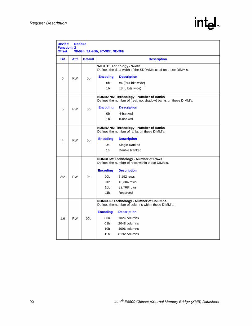
90 Intel® E8500 Chipset eXternal Memory Bridge (XMB) Datasheet
Register Description
6 RW 0b
WIDTH: Technology - WidthDefines the data width of the SDRAM’s used on these DIMM’s.
5 RW 0b
NUMBANK: Technology - Number of BanksDefines the number of (real, not shadow) banks on these DIMM’s.
4 RW 0b
NUMRANK: Technology - Number of RanksDefines the number of ranks on these DIMM’s.
3:2 RW 0b
NUMROW: Technology - Number of RowsDefines the number of rows within these DIMM’s.
1:0 RW 00b
NUMCOL: Technology - Number of Columns Defines the number of columns within these DIMM’s.
Device: NodeIDFunction: 2Offset: 98-99h, 9A-9Bh, 9C-9Dh, 9E-9Fh
Bit Attr Default Description
Encoding Description
0b x4 (four bits wide)1b x8 (8 bits wide)
Encoding Description
0b 4-banked1b 8-banked
Encoding Description
0b Single Ranked1b Double Ranked
Encoding Description
00b 8,192 rows
01b 16,384 rows10b 32,768 rows11b Reserved
Encoding Description
00b 1024 columns01b 2048 columns10b 4096 columns11b 8192 columns

Intel® E8500 Chipset eXternal Memory Bridge (XMB) Datasheet 91
Register Description
4.5.13 DMIR[4:0]: DIMM Interleave Range (F2)These registers define rank participation in various DIMM interleaves. See the DMIR translation algorithm in Section 6.2.8.5, “Address Translation” on page 6-122.
Each register defines a range. If the Memory (M) address falls in the range defined by an adjacent pair of DMIR.LIMIT’s, the ways fields in the upper DMIR define the number and interleave position of ranks’ way participation. Table 4-12 shows how the way-sensitive bits are selected based on presence of 4-bank DIMMs and cache-line size. (If all DIMMs are 8-bank, no 4-bank DIMMs are present.) The way function for {all ranks equal (1 way), 2 cube-adjacent ranks equal but unequal to other ranks (2 way), 2 cube-non-adjacent equal but unequal to other ranks (2 way), all ranks unequal (4 way)} is {“00”, “10”, “01”, “11”} respectively. Matching addresses participate in the corresponding ways. The combination of two equal ranks with three unequal ranks is illegal.
Table 4-12. DIMM Address Way-sensitivity
4-bank DIMM’s present? Cache-Line size way-sensitive M’s
Yes64B [9:8]
128B[10:9]
No64B
128B [11:10]
Device: NodeIDFunction: 2Offset: A0-A3h, A4-A7h, A8-ABh, AC-Afh, B0-B3h
Bit Attr Default Description
31:23 RV 000h Reserved
22:16 RW 00h LIMITThis field defines the highest address in the range. Memory requests participate in this DMIR range if LIMIT[i] > M[35:29] >= LIMIT[i-1]. For i = 0, LIMIT[i-1]=0.
15:13 RV 000b Reserved
12 RW 0b ENABLE
11:9 RW 000b RANK3Defines which rank participates in WAY3.
8:6 RW 000b RANK2Defines which rank participates in WAY2.
5:3 RW 000b RANK1Defines which rank participates in WAY1.
2:0 RW 000b RANK0Defines which rank participates in WAY0.
Encoding Description
0b Memory requests participate in this DMIR range.1b Memory requests do not participate in this DMIR range.

92 Intel® E8500 Chipset eXternal Memory Bridge (XMB) Datasheet
Register Description
4.5.14 RAID: RAID Memory (F2)This register enables RAID functionality on XMB.
4.6 PCI Function 3 - DDR1 Initialization and Calibration(F3)
4.6.1 VID: Vendor Identification Register (F3)This register identifies Intel as the manufacturer of the XMB. Writes to this register have no effect.
4.6.2 DID: Device Identification Register (F3)This register combined with the Vendor Identification register uniquely identifies the XMB. Writes to this register have no effect.
Device: NodeIDFunction: 2Offset: B4h
Bit Attr Default Description
7:1 RV 00h Reserved
0 RW 0ENABLESetting this field places XMB in RAID mode.
Device: NodeIDFunction: 3Offset: 00-01h
Bit Attr Default Description
15:0 RO 8086h Vendor Identification NumberThe value assigned to Intel.
Device: NodeIDFunction: 3Offset: 02-03h
Bit Attr Default Description
15:0 RO 2623h Device Identification Number Identifies each function of the XMB

Intel® E8500 Chipset eXternal Memory Bridge (XMB) Datasheet 93
Register Description
4.6.3 RID: Revision Identification Register (F3)This register contains the revision number of the XMB.
4.6.4 CCR: Class Code Register (F3)This register contains the Class Code for the XMB, specifying the device function.
4.6.5 HDR: Header Type Register (F3)This register identifies the header layout of the configuration space.
Device: NodeIDFunction: 3Offset: 08h
Bit Attr Default Description
7:0 RO 11h Revision Identification Number.“11h” = B1 stepping
Device: NodeIDFunction: 3Offset: 09-0Bh
Bit Attr Default Description
23:16 RO 05h Base Class.This field indicates the general device category. For the XMB, this field is hardwired to 05h, indicating it is a “memory controller”.
15:8 RO 00h Sub-Class.This field qualifies the Base Class, providing a more detailed specification of the device function. For the XMB, this field is hardwired to 00h, indicating it is a “RAM”.
7:0 RO 00h Register-Level Programming Interface.This field identifies a specific programming interface (if any), that device independent software can use to interact with the device. There is no such interface defined for “memory controllers”.
Device: NodeIDFunction: 3Offset: 0E-0Fh
Bit Attr Default Description
7 RO 1b Multi-function Device.Selects whether this is a multi-function device, that may have alternative configuration layouts. The XMB has more than the 256 bytes of configuration registers allotted to a single function. Therefore, the XMB is defined to be a multifunction device, and this bit is hardwired to 1b.
6:0 RO All 0s Configuration Layout.This field identifies the format of the 10h through 3Fh space. The XMB uses header type “00”, and these bits are hardwired to 00h.

94 Intel® E8500 Chipset eXternal Memory Bridge (XMB) Datasheet
Register Description
4.6.6 SVID: Subsystem Vendor Identification Register (F3)This register identifies the manufacturer of the system. This 16-bit register combined with the Device Identification Register uniquely identify any PCI device.
4.6.7 SID: Subsystem Identity (F3)This register identifies the system.
Device: NodeIDFunction: 3Offset: 2C-2Dh
Bit Attr Default Description
15:0 RWO 8086h Vendor Identification Number.The default value specifies Intel’s vendor ID. Each byte of this register will be writeable once. Second and successive writes to a byte will have no effect.
Device: Node_IDFunction: 3Offset: 2E-2Fh
Bit Attr Default Description
15:0 RWO 8086h Subsystem Identification Number: The default value specifies Intel’s vendor ID. Each byte of this register will be writeable once. Second and successive writes to a byte will have no effect.

Intel® E8500 Chipset eXternal Memory Bridge (XMB) Datasheet 95
Register Description
4.6.8 DCALCSR: DCAL Control and Status (F3)
Device: NodeIDFunction: 3Offset: 40-43h
Bit Attr Default Description
31 RWS 0b START: Start Operation. Not preserved by SAVCFG.When set to 1 by software, the operation selected by the dcalcsr.opcode is initiated. Hardware clears this bit when the operation is complete.
30:28 RW 000b FAIL: Completion Status.
27:24 RV 0h Reserved
23 RW 0b ALLP: All passesApplies only to Receive enable, DQS cal
22:20 RW 000b CS: Chip selectApplies only to NOP, Refresh, Precharge all, MRS/EMRS, Receive enable, and DQS cal.
19 RV 0b Reserved
18:16 RW 000b PATTERN: Data pattern for DQS cal and I/O loopback. This sets the burst length 4 pattern for a nibble of data. This pattern is replicated on all nibbles of the data bus.
15 RV 0b Reserved
14:4 RW 000h OPMODS: Operation modifiers
Encoding Description
000b Passx11 Unsupported dcalcsr.opcode1xx Fail
Encoding Description
0b Single pass1b All passes
Encoding Description
000b F > 0 > F > 0001b 0 > F > 0 > F010b A > 5 > A > 5011b 5 > A > 5 > A100b C > 3 > C > 3101b 3 > C > 3 > C
110b 9 > 6 > 9 > 6111b 6 > 9 > 6 > 9

96 Intel® E8500 Chipset eXternal Memory Bridge (XMB) Datasheet
Register Description
3:0 RW 0h OPCODE:
Table 4-13. Special DDR Commands
Command RAS# CAS# WE# BA[1:0] A[13:0] Description
MRS L L L 00 MRS Opcode Mode Register Set Commands:DLL ResetBurst Type/LengthCAS LatencytWR (Write Recovery Time)
EMRS L L L 01 EMRS Opcode
Extended Mode Register Set Commands:DQS# Enable/DisableRDQS Enable/DisableDLL Enable/DisableAdditive Latency
Auto (CBR)
Refresh
L L H XX X Auto Refresh Command:Required for JEDEC initialization sequence.
NOP H H H XX X
Pre-Charge All
Banks
L H L XX A10 = H, X otherwise
Device: NodeIDFunction: 3Offset: 40-43h
Bit Attr Default Description
Encoding Description
0000b NOP
0001b Refresh0010b Pre-Charge0011b MRS/EMRS0100b Receive Enable1110b Error Monitor
All Others Reserved

Intel® E8500 Chipset eXternal Memory Bridge (XMB) Datasheet 97
Register Description
Lightly shaded regions of Table 4-14 indicate bits that are modified by the hardware during DCAL operation.
Table 4-14. Functional Characteristics of DCALCSR
Bit NOP Refresh Pre-charge
MRS / EMRS
Receive Enable
DQS Cal I/O Lpbk DLL BIST ErrorMonitor
31 Start
30
Fail29
28
27
26
25 Channel select24
23 All passes
22
Chip Select21
20
19
18
Data pattern select17
16
15 Disable FIFO reset
14 DLLSlavelength Single
pass DLL slave length
and delay
13
12 Pass2
11Single
pass DLL delay Cycle
wait to allow
master DLL’s to
lock
PTR
10Read
pointer9
Receive enabledelay
used in singlepass
8
7Receive enabledelay
6
5
4
3
Opcode2
1
0

98 Intel® E8500 Chipset eXternal Memory Bridge (XMB) Datasheet
Register Description
DCALCSR OPMODS in Receive enable mode
Bit Description
9:4 Receive enable delay used in single pass: This sets the delay of the strobe receiver enable signal when single pass is selected. The delay is in terms of CMDCLK cycles. The lower 3 bits set the fractional delay from 3/8 to 10/8 of a cycle, and the upper 3 bits select whole cycle delays. The whole cycle delays are measured from the issue of a READ command from the core to the issue of the enable signal from the core. These parameters are varied automatically in all pass mode.
DCALCSR OPMODS in DQS cal mode
Bit Description
11:8 Fine DLL delay: Provides fine adjustment of the DLL delay.
DCALCSR OPMODS in I/O loopback mode
Bit Description
14:8 Single pass DLL slave length and delay: This sets both the DLL slave length and DLL delay when single pass mode is selected. Both these parameters are varied automatically when all pass mode is selected.
6:4 Receive enable delay: This sets the fractional cycle delay of the strobe receiver enable signal. The delay can be set from 3/8 to 2 1/4 CMDCLK cycles.
DCALCSR OPMODS in DLL BIST mode
Bit Description
12 Pass2: When single pass mode is selected, this bit controls whether the 1st or 2nd pass of the DLL BIST algorithm is executed. Setting this bit to 1 selects the 2nd pass.
11:4 Cycle wait to allow master DLL’s to lock: This sets the number of core cycles to wait after the DCALADDR.MASTLEN/MIX values are sent to the DLL’s before issuing the biststart signal from the core to put the slave elements in self oscillation mode.
DCALCSR OPMODS in Error monitor mode
Bit Description
10:8 Read pointer: This sets the DDR cluster inbound data fifo read pointer when the PTR bit is set to zero. In this mode fifo contents from this one pointer location is read into the core and stored in the DCALDATA registers.
6 PTR: When set to 1 the error monitor reads the DDR cluster inbound data fifo write pointer setting into the core and stores it in the DCALDATA registers.

Intel® E8500 Chipset eXternal Memory Bridge (XMB) Datasheet 99
Register Description
4.6.9 DCALADDR: DCAL Address RegisterTable 4-15. Functional Characteristics of DCALADDR
Bit NOP, Refresh, Precharge, MRS/EMRS, Receive Enable, DQS Cal
I/O Lpbk DLL BIST Error Monitor,
31
30
29
Row Address 13:0
Pass2 Masterlen28
27
Pass2 Mastermix26
25
24
23
22
21
Max delta first to last DLL delay
Pass1 Masterlen20
19
Pass1 Mastermix18
17
16
15
14
Pass2 Slavelen13
Column Address 12, 11, 9:2
Max first all fail
DLL delay
12
11
Pass2 Slavemix10
9
8
7
6Pass1 Slavelen
5
Min First fail DLL delay
4
3
Pass1 Slavelen2
Bank Address 2:01
0
Device: NodeIDFunction: 3Offset: 44-47h
Bit Attr Default Description
31:0 RW 0000_0000h DCALADDR: DCAL Address and Other Information Based on Opcode.

100 Intel® E8500 Chipset eXternal Memory Bridge (XMB) Datasheet
Register Description
4.6.10 DCALDATA[71:0]: DCAL Data Registers (F3)
Device: NodeIDFunction: 3Offset: 48h - 8Fh
Bit Attr Default Description
7:0 RW 00h DCALDATA: DCAL Data and Other Information Based on Opcode.
I/O Loopback DCALDATA “All Fail” byte detail
Bit Description
7 All fail found: All data in burst fails at associated nibble. When set, no further updates are made in this byte.
6 Last all fail found: This bit indicates that the byte was the last to have its “All fail found” bit set. This will be the largest recorded slavelen/mix (bits 5 to 0) of any “All fail” byte.
5:4 Slavelen when bit 7 is set.
3:0 Slavemix when bit 7 is set.
I/O Loopback DCALDATA “1st Fail” byte detail
Bit Description
7 1st fail found: At least one bit in a burst fails at the associated nibble. When set, no further updates are made in this byte.
6 First 1st fail: This bit indicates that the byte was the first to have its “1st fail found” bit set. This will be the smallest recorded slavelen/mix (bits 5 to 0) of any “1st fail” byte.
5:4 Slavelen when bit 7 is set.
3:0 Slavemix when bit 7 is set.

Intel® E8500 Chipset eXternal Memory Bridge (XMB) Datasheet 101
Register Description
Lightly shaded regions of Table 4-16 indicate bits that are modified by the hardware during DCAL operation.
Table 4-16. Functional Characteristics of DCALDATA
Byte NOP, Refresh, Pre-charge MRS / EMRS Receive
Enable DQS Cal I/O Lpbk DLL BIST Error MonitorDCALCSR.PTR=1
Error MonitorDCALCSR.PTR=0
71 Adjust 1_17 Wrptr high Pass[15:0] 1_17
All Fail 1_17 DQS17 counter70 Adjust 1_8 Wrptr low 1st Fail 1_17
69 Adjust 0_17 Ch1 OR’d Pass[15:0] 1_8
All Fail 1_8 DQS8 counter Ch1 OR’d68 Adjust 0_8 Ch0 OR’d 1st Fail 1_8 Ch0 OR’d67 Drive 1_17 Wrptr 1_17 Pass[15:0]
0_17All Fail 0_17 DQS16
counterWrptr 1_17 Ch1 late CB
66 Drive 1_8 Wrptr 1_8 1st Fail 0_17 Wrptr 1_8 Ch1 early CB65 Drive 0_17 Wrptr 0_17 Pass[15:0]
0_8All Fail 0_8 DQS7 counter Wrptr 0_17 Ch0 late CB
64 Drive 0_8 Wrptr 0_8 1st Fail 0_8 Wrptr 0_8 Ch0 early CB63 Adjust 1_16 Wrptr 1_16 Pass[15:0]
1_16All Fail 1_16 DQS15
counterWrptr 1_16
62 Adjust 1_7 Wrptr 1_7 1st Fail 1_16 Wrptr 1_761 Adjust 1_14 Wrptr 1_14 Pass[15:0]
1_14All Fail 1_14 DQS6 counter Wrptr 1_14
60 Adjust 1_5 Wrptr 1_5 1st Fail 1_14 Wrptr 1_559 Adjust 1_12 Wrptr 1_12 Pass[15:0]
1_12All Fail 1_12 DQS14
counterWrptr 1_12
58 Adjust 1_3 Wrptr 1_3 1st Fail 1_12 Wrptr 1_357 Adjust 1_10 Wrptr 1_10 Pass[15:0]
1_10All Fail 1_10 DQS5 counter Wrptr 1_10
56 Adjust 1_1 Wrptr 1_1 1st Fail 1_10 Wrptr 1_155 Adjust 1_15 Wrptr 1_15 Pass[15:0]
1_15All Fail 1_15 DQS13
counterWrptr 1_15
54 Adjust 1_6 Wrptr 1_6 1st Fail 1_15 Wrptr 1_653 Adjust 1_13 Wrptr 1_13 Pass[15:0]
1_13All Fail 1_13 DQS4 counter Wrptr 1_13
52 Adjust 1_4 Wrptr 1_4 1st Fail 1_13 Wrptr 1_451 Adjust 1_11 Wrptr 1_11 Pass[15:0]
1_11All Fail 1_11 DQS12
counterWrptr 1_11
50 Adjust 1_2 Wrptr 1_2 1st Fail 1_11 Wrptr 1_249 Adjust 1_9 Wrptr 1_9 Pass[15:0]
1_9All Fail 1_9 DQS3 counter Wrptr 1_9
48 Adjust 1_0 Wrptr 1_0 1st Fail 1_9 Wrptr 1_047 Adjust 0_16 Wrptr 0_16 Pass[15:0]
0_16All Fail 0_16 DQS11 counter Wrptr 0_16
46 Adjust 0_7 Wrptr 0_7 1st Fail 0_16 Wrptr 0_745 Adjust 0_14 Wrptr 0_14 Pass[15:0]
0_14All Fail 0_14 DQS2 counter Wrptr 0_14
44 Adjust 0_5 Wrptr 0_5 1st Fail 0_14 Wrptr 0_543 Adjust 0_12 Wrptr 0_12 Pass[15:0]
0_12All Fail 0_12 DQS10
counterWrptr 0_12
42 Adjust 0_3 Wrptr 0_3 1st Fail 0_12 Wrptr 0_341 Adjust 0_10 Wrptr 0_10 Pass[15:0]
0_10All Fail 0_10 DQS1 counter Wrptr 0_10
40 Adjust 0_1 Wrptr 0_1 1st Fail 0_10 Wrptr 0_139 Adjust 0_15 Wrptr 0_15 Pass[15:0]
0_15All Fail 0_15 DQS9 counter Wrptr 0_15
38 Adjust 0_6 Wrptr 0_6 1st Fail 0_15 Wrptr 0_637 Adjust 0_13 Wrptr 0_13 Pass[15:0]
0_13All Fail 0_13 DQS0 counter Wrptr 0_13
36 Adjust 0_4 Wrptr 0_4 1st Fail 0_13 Wrptr 0_435 Adjust 0_11 Wrptr 0_11 Pass[15:0]
0_11All Fail 0_11 Core interval
counterWrptr 0_11
34 Adjust 0_2 Wrptr 0_2 1st Fail 0_11 Wrptr 0_233 Adjust 0_9 Wrptr 0_9 Pass[15:0]
0_9All Fail 0_9 Core counter Wrptr 0_9
32 Adjust 0_0 Wrptr 0_0 1st Fail 0_9 Wrptr 0_031 Drive 1_16
Ch1 DQS Sampled
High
Pass[15:0] 1_7
All Fail 1_7
First edge counters, First edge status,
Terminal count in process bits,
Fail vectors, Pass window shift register, and 2nd pass
minimum count
Ch1 late DQ
30 Drive 1_7 1st Fail 1_729 Drive 1_14 Pass[15:0]
1_5All Fail 1_5
28 Drive 1_5 1st Fail 1_527 Drive 1_12 Pass[15:0]
1_3All Fail 1_3
26 Drive 1_3 1st Fail 1_325 Drive 1_10 Pass[15:0]
1_1All Fail 1_1
24 Drive 1_1 1st Fail 1_123 Drive 1_15
Ch1 DQS Sampled
Low
Pass[15:0] 1_6
All Fail 1_6
Ch1 early DQ
22 Drive 1_6 1st Fail 1_621 Drive 1_13 Pass[15:0]
1_4All Fail 1_4
20 Drive 1_4 1st Fail 1_419 Drive1_11 Pass[15:0]
1_2All Fail 1_2
18 Drive 1_2 1st Fail 1_217 Drive 1_9 Pass[15:0]
1_0All Fail 1_0
16 Drive 1_0 1st Fail 1_015 Drive 0_16
Ch0 DQS Sampled
High
Pass[15:0] 0_7
All Fail 0_7
Ch0 late DQ
14 Drive0 _7 1st Fail 0_713 Drive 0_14 Pass[15:0]
0_5All Fail 0_5
12 Drive 0_5 1st Fail 0_511 Drive 0_12 Pass[15:0]
0_3All Fail 0_3
10 Drive 0_3 1st Fail 0_39 Drive 0_10 Pass[15:0]
0_1All Fail 0_1 Terminal DQS
count8 Drive 0_1 1st Fail 0_17 Drive 0_15
Ch0 Sampled
Low
Pass[15:0] 0_6
All Fail 0_6 2nd pass delta count
Ch0 early DQ
6 Drive 0_6 1st Fail 0_65 Drive 0_13 Pass[15:0]
0_4All Fail 0_4 2nd pass offset4 Drive 0_4 1st Fail 0_4
3 Drive 0_11 Pass[15:0] 0_2
All Fail 0_2 1st pass delta count2 Drive 0_2 1st Fail 0_2
1 Drive 0_9 Pass[15:0] 0_0
All Fail 0_0 1st passminimum count0 Drive 0_0 1st Fail 0_0

102 Intel® E8500 Chipset eXternal Memory Bridge (XMB) Datasheet
Register Description
DCALDATA is a set of general-purpose data registers that are used by most of the DCAL operations. It consists of 72 Bytes of storage that are read/writeable through configuration registers. In addition, several of the operations have the ability to write all or portions of these registers.
DLL BIST DCALDATA bytes 31 to 8 detail
Bit Bytes 31 to 28
Bytes 27 to 24
Bytes 23 to 20
Bytes 19 to 16
Bytes 15 to 12
Bytes 11 to 8
31
DQS17 first edge counter
DQS8 first edgecounter
DQS16 first edge counter
DQS7 first edge counter
DQS15 first edgecounter
DQS6 first edge counter
30
29
28
27
DQS14 first edge counter
DQS5 first edgecounter
DQS13 first edge counter
DQS4 first edge counter
DQS12 first edgecounter
DQS3 first edge counter
26
25
24
23
DQS11 first edge counter
DQS2 first edgecounter
DQS10 first edge counter
DQS1 first edge counter
DQS9 first edgecounter
DQS0 first edge counter
22
21
20
19 DQS17 first edge fail
DQS16 first edge fail
DQS15 first edge fail
DQS14 first edge fail
DQS12 first edge fail
DQS10 first edge fail
18 DQS8 first edge fail DQS7 first edge fail DQS6 first edge fail DQS5 first edge fail DQS3 first edge fail DQS1 first edge fail
17 DQS17 in process Ch1 DQS17 fail Ch0 DQS17 fail DQS13 first edge fail
DQS11 first edge fail DQS9 first edge fail
16 DQS8 in process Ch1 DQS8 fail Ch0 DQS8 fail DQS4 first edge fail DQS2 first edge fail DQS0 first edge fail
15 DQS16 in process Ch1 DQS16 fail Ch0 DQS16 fail
Passwindow shift register
2nd pass minimum count writtenduring 1st pass
DQSterminal count
14 DQS7 in process Ch1 DQS7 fail Ch0 DQS7 fail
13 DQS15 in process Ch1 DQS15 fail Ch0 DQS15 fail
12 DQS6 in process Ch1 DQS6 fail Ch0 DQS6 fail
11 DQS14 in process Ch1 DQS14 fail Ch0 DQS14 fail
10 DQS5 in process Ch1 DQS5 fail Ch0 DQS5 fail
9 DQS13 in process Ch1 DQS13 fail Ch0 DQS13 fail
8 DQS4 in process Ch1 DQS4 fail Ch0 DQS4 fail
7 DQS12 in process Ch1 DQS12 fail Ch0 DQS12 fail
6 DQS3 in process Ch1 DQS3 fail Ch0 DQS3 fail
5 DQS11 in process Ch1 DQS11 fail Ch0 DQS11 fail
4 DQS2 in process Ch1 DQS2 fail Ch0 DQS2 fail
3 DQS10 in process Ch1 DQS10 fail Ch0 DQS10 fail
2 DQS1 in process Ch1 DQS1 fail Ch0 DQS1 fail
1 DQS9 in process Ch1 DQS9 fail Ch0 DQS9 fail
0 DQS0 in process Ch1 DQS0 fail Ch0 DQS0 fail

Intel® E8500 Chipset eXternal Memory Bridge (XMB) Datasheet 103
Register Description
This register is used for the following purposes:
• Receive Enable Calibration: Two expected write pointer values are written by software. The rest of the register space is written by hardware and read by software. The expected write pointers are compared against the “or” of all the write pointers read out of the DDR cluster FIFO’s. The sampled high/low fields are written with the compare results at each of 64 different strobe receiver enable settings. This data is used to set the DRRTC0/1 registers.
• DQS Calibration: The entire register space is written with test results by hardware and read by software. There are two bytes of test results for each strobe, one bit for each possible setting of the fine on chip strobe delay called Slavemix. This data is used to set the DQSOFCSL/M/H registers.
• Error Monitor: The register space is used differently depending on the error monitor mode bit DCALCSR.PTR. When PTR is set to one, the DDR cluster FIFO contents at one read pointer address are read out of the cluster and stored in half of the register space. When PTR is set to zero, write pointer information is read out of the cluster and stored in the same format as for Receiver Enable Calibration.
4.6.11 DRRTC[1:0]: Receive Enable Reference Output TimingControl Register (F3)This register determines DQS input buffer enable timing delay. A proper selection will delay the start of the DQS input receiver enable window so that it coincides with the middle of the DQS pre-amble. Enabling the window before or after the pre-amble would cause valid DQS edges to be missed or invalid edges or noise to be received.
This register controls the enable delay with a minimum of 2.375 CMDCLK’s and a maximum of 10.25 CMDCLK’s, in 0.125 CMDCLK increments. The delay is measured from the clock edge that a READ command sent from the core is received in the DDR cluster to the time the DDR cluster DQS input receiver is enabled. The total delay can be broken into the number of whole CMDCLK cycles counted in the core, and the number of fractional CMDCLK increments counted in the DDR cluster. The three LSB’s of the RCVEN field sets the number of fractional increments from 0.375 to 1.25 CMDCLK’s. The upper three MSB’s of RCVEN set the number of CMDCLK cycles counted in the core before sending the enable and fractional control signals to the cluster.
In DDR1 mode where 8-ranks are supported, the strobes are calibrated by “socket”, so adjacent rank pairs use the same delay. In DDR2 mode, where the maximum number of ranks is limited to 4 due to system considerations, there is a unique delay for each rank for all valid DIMM loading configurations. The two channels spanning the ranks are calibrated separately.
Device: NodeIDFunction: 3Offset: 94-97h, 90-93h
Bit Attr Default Description
31:30 RV 00b Reserved
29:24 RW 00h RCVEN3: RCVEN Delay Code, Channel 1/0DDR1 Mode: selected by CS6 and CS7DDR2 Mode: selected by CS6 and CS1
23:22 RV 00b Reserved

104 Intel® E8500 Chipset eXternal Memory Bridge (XMB) Datasheet
Register Description
4.6.12 DQSOFCSL[7:0] Low DQS Calibration Registers (F3)The DQSOFCS{L/M/H}[7:0] registers contain 4-bit delays necessary for proper capture of the DQS and DQS# read strobes received by the DDR channels. The “Description” fields of each table enumerate the strobes that are calibrated by the corresponding delay value.
In DDR mode where 8-ranks are supported, the strobes are calibrated by “socket”, so adjacent rank pairs use the same offset, as shown in Table 4-17. In DDR2 mode, where the maximum number of ranks is limited to 4 due to system considerations, there is a unique offset for each rank for all valid DIMM loading configurations. The two channels spanning the ranks are calibrated separately.
21:16 RW 00h RCVEN2: RCVEN Delay Code, Channel 1/0DDR1 Mode: selected by CS4 and CS5DDR2 Mode: selected by CS4 and CS3
15:14 RV 00b Reserved
13:8 RW 00h RCVEN1: RCVEN Delay Code, Channel 1/0DDR1 Mode: selected by CS2 and CS3DDR2 Mode: selected by CS2
7:6 RV 00b Reserved
5:0 RW 00h RCVEN0: RCVEN Delay Code, Channel 1/0DDR1 Mode: selected by CS0 and CS1DDR2 Mode: selected by CS0
Device: NodeIDFunction: 3Offset: 94-97h, 90-93h
Bit Attr Default Description
Table 4-17. Register Number Mapping
Register Channel DDR-I Mode CS Mapping DDR-II Mode CS Mapping
0
0
0 & 1 0
1 2 & 3 2
2 4 & 5 4 & 3
3 6 & 7 6 & 1
4
1
0 & 1 0
5 2 & 3 2
6 4 & 5 4 & 3
7 6 & 7 6 & 1

Intel® E8500 Chipset eXternal Memory Bridge (XMB) Datasheet 105
Register Description
4.6.13 DQSOFCSM[7:0] Middle DQS Calibration Registers (F3)
4.6.14 DQSOFCSH[7:0] High DQS Calibration Registers (F3)
Device: NodeIDFunction: 3Offset: F4-F7h, E8-EBh, DC-DFh, D0-D3h, C4-C7h, B8-EBh, AC-AFh, A0-A3h
Bit Attr Default Description
31:28 RW 0h DQS7: Offset
27:24 RW 0h DQS6: Offset
23:20 RW 0h DQS5: Offset
19:16 RW 0h DQS4: Offset
15:12 RW 0h DQS3: Offset
11:8 RW 0h DQS2: Offset
7:4 RW 0h DQS1: Offset
3:0 RW 0h DQS0: Offset
Device: NodeIDFunction: 3Offset: F8-FBh, EC-EFh, E0-E3h, D4-D7h, C8-CBh, BC-BFh, B0-B3h, A4-A7h
Bit Attr Default Description
31:28 RW 0h DQS15: Offset
27:24 RW 0h DQS14: Offset
23:20 RW 0h DQS13: Offset
19:16 RW 0h DQS12: Offset
15:12 RW 0h DQS11: Offset
11:8 RW 0h DQS10: Offset
7:4 RW 0h DQS9: Offset
3:0 RW 0h DQS8: Offset
Device: NodeIDFunction: 3Offset: FCh, F0h, E4h, D8h, CCh, C0h, B4h, A8h
Bit Attr Default Description
7:4 RW 0h DQS17: Offset
3:0 RW 0h DQS16: Offset

106 Intel® E8500 Chipset eXternal Memory Bridge (XMB) Datasheet
Register Description
4.7 PCI Function 4,5,6,7 - Reserved
4.7.1 VID: Vendor Identification Register This register identifies Intel as the manufacturer of the XMB. Writes to this register have no effect.
4.7.2 DID: Device Identification Register This register combined with the Vendor Identification register uniquely identifies the XMB. Writes to this register have no effect.
4.7.3 RID: Revision Identification Register This register contains the revision number of the XMB.
Device: NodeIDFunction: 4, 5, 6, 7Offset: 00-01h
Bit Attr Default Description
15:0 RO 8086h Vendor Identification NumberThe value assigned to Intel.
Device: NodeIDFunction: 4, 5, 6, 7Offset: 02-03h
Bit Attr Default Description
15:0 RO See description
Device Identification Number Identifies each function of the XMB
Function Device Number
4 2624h5 2625h6 2626h7 2627h
Device: NodeIDFunction: 4, 5, 6, 7Offset: 08h
Bit Attr Default Description
7:0 RO 11h Revision Identification Number.“11h” = B1 stepping

Intel® E8500 Chipset eXternal Memory Bridge (XMB) Datasheet 107
Register Description
4.7.4 CCR: Class Code Register This register contains the Class Code for the XMB, specifying the device function.
4.7.5 HDR: Header Type Register This register identifies the header layout of the configuration space.
Device: NodeIDFunction: 4, 5, 6, 7Offset: 09-0Bh
Bit Attr Default Description
23:16 RO 05h Base Class.This field indicates the general device category. For the XMB, this field is hardwired to 05h, indicating it is a “memory controller”.
15:8 RO 00h Sub-Class.This field qualifies the Base Class, providing a more detailed specification of the device function. For the XMB, this field is hardwired to 00h, indicating it is a “RAM”.
7:0 RO 00h Register-Level Programming Interface.This field identifies a specific programming interface (if any), that device independent software can use to interact with the device. There is no such interface defined for “memory controllers”.
Device: NodeIDFunction: 4, 5, 6, 7Offset: 0E-0Fh
Bit Attr Default Description
7 RO 1b Multi-function Device.Selects whether this is a multi-function device, that may have alternative configuration layouts. The XMB has more than the 256 bytes of configuration registers allotted to a single function. Therefore, the XMB is defined to be a multifunction device, and this bit is hardwired to 1b.
6:0 RO All 0s Configuration Layout.This field identifies the format of the 10h through 3Fh space. The XMB uses header type “00”, and these bits are hardwired to 00h.

108 Intel® E8500 Chipset eXternal Memory Bridge (XMB) Datasheet
Register Description
4.7.6 SVID: Subsystem Vendor Identification Register This register identifies the manufacturer of the system. This 16-bit register combined with the Device Identification Register uniquely identify any PCI device.
§
Device: NodeIDFunction: 4, 5, 6, 7Offset: 2C-2Dh
Bit Attr Default Description
15:0 RWO 8086h Vendor Identification Number.The default value specifies Intel’s vendor ID. Each byte of this register will be writeable once. Second and successive writes to a byte will have no effect.

Intel® E8500 Chipset eXternal Memory Bridge (XMB) Datasheet 109
5 System Address Map
The system address map is defined in Chapter 5 of the latest version of the Intel® E8500 Chipset North Bridge (NB) Datasheet.
§

110 Intel® E8500 Chipset eXternal Memory Bridge (XMB) Datasheet
System Address Map

Intel® E8500 Chipset eXternal Memory Bridge (XMB) Datasheet 111
6 Functional Description
This chapter describes the operation of the major functional units of the Intel® E8500 chipset eXternal Memory Bridge (XMB).
6.1 Independent Memory InterfaceThis section defines the XMB’s Independent Memory Interface (IMI). The IMI is a packet-based point-to-point chip interconnect between the XMB and NB. It’s a fully simultaneous bi-directional interface with a write bandwidth to the XMB of 2.67 GB/s and a read bandwidth from the XMB of 5.33 GB/s
The inbound data path consists of 16 data bits, 2 ECC bits and 3 link bits. The outbound data path consists of 10 bits of data and CRC, and link information.
6.1.1 Outstanding RequestsThe XMB supports a maximum of 16 pending read and 16 pending write requests over the IMI.
Stop-based write flow control will be exercised when the write queue depth is greater than or equal to MC.WPQLIM. The XMB can accept (16 - MIC.WPQULIM) more writes after this threshold is reached.
6.1.2 LatencyAt full speed, the XMB guarantees that any memory transaction is completed within 8 µs after accepting the request from the IMI.
6.1.3 Hot Add and RemoveThe hot add and remove functions are largely controlled by the Intel® E8500 chipset North Bridge (NB) and at the platform level. The XMB does not provide explicit support for hot add and remove, except for the following:
For hot removal, within 200 ns of the assertion of RST#, the IMI outbound drivers and termination will turn off. The XMB.IMI expects the IMI inbound interface to remain valid for at least 100 ns after the assertion of RST# to guarantee that spurious errors are not logged before reset. PWRGOOD should be de-asserted before the removal of power.
For hot removal and addition, PWRGOOD and RST# should follow normal power off/on sequencing, as described in “Reset” on page 6-147 of this document.

112 Intel® E8500 Chipset eXternal Memory Bridge (XMB) Datasheet
Functional Description
6.1.4 InitializationThe NB and XMB implementations share much of the initialization design. Other portions of initialization are NB-specific, as NB controls add and removal, and RAID across multiple IMI link. See the Intel® E8500 Chipset North Bridge (NB) Datasheet for more information on the initialization sequence. The following sections discuss the XMB specific implementation.
6.1.4.1 Physical and Link Layer Initialization
The initialization sequence is triggered by the de-assertion of RST#.
The XMB implements one global count-down timer for the entire initialization sequence. If the timer reaches zero before the link comes up, the link will be forced into a Reset state. The only way to remove XMB from this state is to reset the XMB (i.e. assert, then de-assert, RST#).
This timer is a programmable register, IMILNKINIT.TMRCOUNT. The default value will count 10ms. If the value needs to be changed, and the link is not up, then it cannot be written in configuration address space, but must be written via JTAG or SMBUS. The register is sticky across resets.
The XMB does not support a low power state if port presence detection fails. Assertion of RST# (except for certain test modes) will turn off the drivers and the termination.
6.1.4.2 Parameter Passing (MAPR and MOFF)
Immediately after the IMI link comes up, the XMB.IMI will be in a default state in which the MOFF register will contain the value 2, and the MAPR register will contain the value 7. Only configuration space accesses will be supported at this time. Memory space reads will be ignored. Configuration read returns will use a header offset value of 2.
Link initialization must be completed by passing operating parameters from the NB to the XMB through the IMI.
The only values XMB supports for MLINE (cache-line size), XMBNK (critical chunk size), and MCODE (ECC code), are 0, 0, and 3, respectively. The value 0 for MLINE encodes the value 64bytes, and the value 0 for XMBNK encodes the value 16bytes. The value 3 for MCODE is the encoding for the x8 SDDC ECC code used by XMB. These are the default values for these registers, and there is no need to pass these parameters. If any value other than a supported value is written, the configuration write will terminate with a Write Abort, and the value in the register will not be changed.
The values that need to be set to complete link initialization are the values for MAPR (aperture), and MOFF (header offset).
To complete link initialization, software must read the values from MIC.MAPRINIT and MIC.MOFFINIT and write them into MAPR and MOFF. MAPR must be written first, followed by MOFF. Until MOFF has been changed from the value 2, memory reads will be ignored. After MOFF has been written with a supported value, the link will return both configuration return data and memory read return data using the new header offset and aperture.
If any value other than the supported value for MAPR is written, the configuration write will terminate with a Write Abort, and the value in the MAPR register will not be changed.

Intel® E8500 Chipset eXternal Memory Bridge (XMB) Datasheet 113
Functional Description
If any value other than the supported value for MOFF is written, or, if the MAPR register does not already contain the supported value for MAPR when MOFF is written, the configuration write to MOFF will terminate with a Write Abort, and the value in the MOFF register will not be changed.
6.1.5 Outbound InterfaceThe XMB IMI outbound interface receives commands and data packets from the NB and performs CRC error checking on them. packets with CRC errors are dropped and logged, and may result in transaction timeouts. All commands received without CRC errors will have a response (read return, read abort, write ack or write abort) generated at the IMI inbound interface.
Write data can be accepted at the full link bandwidth.
6.1.5.1 Configuration Commands
All configuration registers on the XMB are 1-4 bytes. The XMB IMI supports 0-4 byte writes to configuration registers, using any combination of the four least significant byte mask bits. Byte mask bits are ignored on configuration reads.
6.1.6 XMI Inbound InterfaceThe XMB IMI inbound interface generates responses to all commands received on the outbound interface. Read commands will be acknowledged with either read return data, or a Read Abort. Write commands will be acknowledged with either a Write Ack or a Write Abort. In addition, the inbound interface will deliver in-band signals which are not associated with a specific transaction and training idles (when necessary) to maintain the required transition density on the IMI link.
6.1.6.1 Read Returns and Aborts
Read returns consist of a header and a full cache-line of data and ECC. Data and ECC are taken from the DIMMs and delivered with no modification. If ECC indicates an error, the error is not corrected before sending the data to the NB.IMI.
The ECC code is chosen and laid out such that in addition to the coverage provided for a failed memory component, it provides coverage of single wire faults on the IMI link.
The first 32 bytes of read return data will be returned in contiguous packets, uninterrupted by idle packets. The second 32 bytes of read return data will also be returned in contiguous packets, uninterrupted by idle packets. There may or may not be idle packets between the first 32 bytes and second 32 bytes of data. Idle packets will always be generated in pairs, i.e. there will always be an even number of contiguous idle packets.
Configuration Reads always return a full cache-line worth of data (64 bytes), with the 4 bytes of configuration register data as the least significant four bytes. In addition, XMB IMI will return configuration data in bytes 0-3, 4-7, 8-11, 12-15, 32-35, 36-39, 40-43, and 44-47 of the 64 byte data return to assist NB in placing the data on the FSB. The remaining data bytes will be all zeros.
Read aborts are indicated by a bit in the link layer, and contain all ones in the data bytes with valid ECC. See the Intel® E8500 Chipset North Bridge (NB) Datasheet for more information about the generation and handling of read aborts.

114 Intel® E8500 Chipset eXternal Memory Bridge (XMB) Datasheet
Functional Description
6.1.6.2 Write Acknowledgments and Aborts
Write acknowledgments for Memory Writes are generated after the write has been posted to the XMB write request queue. This happens after receipt of a valid write command followed by a full cache-line of error free data. Write acknowledgments for Memory Writes are generated at the full bandwidth of the Memory Writes, so no flow control on outstanding writes is necessary. The maximum number of outstanding (non-acknowledged) writes depends on the round-trip latency from the NB.IMI sending the last data flit to the NB.IMI receiving and decoding the Write Acknowledgement.
If the Memory Write cannot be posted, then a Write Abort will be generated. See the Intel® E8500 Chipset North Bridge (NB) Datasheet for more information about the generation and handling of write aborts.
Write acknowledgements for Configuration Writes are generated after the data has been successfully written to the configuration register.
Configuration Writes will not generate Write Aborts, except for the special cases involved with IMI initialization, discussed in Section 6.1.4, “Initialization” .
6.1.7 In-band Error SignalsIn addition to Memory and Configuration Read Returns and Write Acknowledgements, the inbound interface can deliver in-band asynchronous signals. They are used to signal error events or other events that are not associated with a specific transaction.
Delivery of certain in-band signals is assured by repetition until the source of the in-band signal is cleared. Table 6-1 shows which in-band signals are sent only once for each event that triggers them, and which ones are sent repeated until the source is cleared:
Table 6-1. IMI In-Band Signals
Signal[4:0]Encoding Signal Repeated Source
0h Correctable Error Yes {FERR | NERR}.Correctable
1h Uncorrectable Error Yes {FERR | NERR}.Uncorrectable
2h Fatal Error Yes {FERR | NERR}.Fatal
4h Second Read Return Header No Read Data
11h Interrupt Yes MC.{LBTHR | SFO}
12h Reserved Yes Reserved
18h Refresh Cycle Complete No Refresh
1Ch Reserved Yes
Reserved1Dh Reserved Yes
1Eh Reserved Yes
1Fh Reserved Yes

Intel® E8500 Chipset eXternal Memory Bridge (XMB) Datasheet 115
Functional Description
6.1.8 Flow ControlXMB IMI supports flow control. This section describes a few implementation specific details.
6.1.8.1 Command Throttling
Commands cannot necessarily be accepted at the full link bandwidth. The rate at which commands can be accepted is a function of the XMB core frequency. Table 6-2 specifies IMI command throttling values to prevent command buffer over-run. The ratio of NB.IMI_Throttle_Cmds to NB.IMI_Throttle_Duration must be less than or equal to the ratio of XMB.IMI_Throttle_Cmds to XMB.IMI_Throttle_Duration.
6.1.9 Command Back Pressure
6.1.9.1 Flow Control of Memory Reads
XMB support a maximum of 16 outstanding Memory Reads. If additional read requests are received above this limit, they may be discarded and logged.
6.1.9.2 Max Outstanding Memory Writes
Write acknowledgments for Memory Writes are generated after the write has been posted to the XMB write request queue. This happens after receipt of a valid write command followed by a full cache-line of error free data. Since write acknowledgments for Memory Writes are generated at the full bandwidth of the Memory Writes, the maximum number of outstanding (non-acknowledged) writes depends on the round-trip latency from the NB.IMI sending the last data flit to the NB.IMI receiving and decoding the Write Acknowledgement. See the Intel® E8500 Chipset North Bridge (NB) Datasheet for more details.
6.1.9.3 Go Bit
XMB can store up to 16 posted writes (writes that have been acknowledged, but not yet completed). Flow control for the posted write queue is provided by the go bit, as described below.
Go bit assertion is controlled by IMIC.WPQLLIM and IMIC.WPQULIM, programmable thresholds for the posted write queue. Correct values for these thresholds depend on the maximum number of write commands that the XMB can receive after the XMB decides to stop memory writes. This is a function of the round trip latency from the cycle in which XMB IMI decides to assert the go bit through the cycle, through the NB.IMI decoding the go bit and stopping issue of write commands, to the XMB receiving the remaining write commands in flight.
The correct value of the MIC.WPQLLIM and the MIC.WPQULIM will depend on the reaction time of the NB.IMI.
Table 6-2. IMI Command Throttling Ratios
DDR Frequency IMI Frequency XMB Core Frequency XMI_Throttle_Cmds XMI_Throttle_Duration
266 MHz 2.67 GHz 266 MHz 4 5
333 MHz 2.67 GHz 167 MHz 1 2
400 MHz 2.67 GHz 200 MHz 3 5

116 Intel® E8500 Chipset eXternal Memory Bridge (XMB) Datasheet
Functional Description
6.1.9.4 Flow Control of Configuration Commands
Only one configuration command can be outstanding at a time, and the toggle bit (TT) is used to detect retried configuration commands. If the XMB receives a configuration read with the same toggle bit value as the previous configuration command, it will assume this is a retried read, and will return the previously sent configuration data without re-accessing the configuration registers. If the XMB receives a configuration write with the same toggle bit value as the previous configuration command it will assume this is a retried write, and will acknowledge the write without performing it.
6.1.10 Error HandlingIMI outbound commands and data, inbound data, data in the DIMMs, and data in transit through XMB are protected by a number of different mechanisms described in “Reliability, Availability, and Serviceability” on page 6-137.
In general, for error types on an IMI command that are likely to be transient, the error is logged, and the command is not acknowledged. The command will time-out, and the IMI.NB should retry the command. For error types that would likely persist through a retry, the XMB.IMI will terminate the command with a read abort or write abort. NB can be programmed to respond to aborts in a number of different ways, but will not retry an aborted command.
If Memory Write data is marked as “poisoned”, the write will be acknowledged, the data will be poisoned in memory, and an error will be logged. If Configuration Write data is marked as “poisoned”, the write will be aborted and an error will be logged.
Logged errors will cause in-band signals to be generated on the inbound IMI interface, as described in Section 4.4.30, “FERR: First Error (F1)” on page 4-70 of this document.
The following errors will be logged, and the command will be allowed to time-out.• Outbound CRC Error• Too many or too few write data packets (likely associated with outbound CRC error)• Read request overflow• Write post queue overflow• More than one configuration command in progress
The following errors will cause either a read abort or a write abort.• Device Commands• Partial Memory Writes• Rejected IMI write to “rrw” register (likely issued during IMI initialization sequence)• Configuration Write with poisoned data• Out-of-range memory access
The following error will be logged as an uncorrectable error.• Command Throttle Limit Exceeded
The following error will be logged as a correctable error.• Memory Write with poisoned data
The above list of errors is not a complete list of XMB errors, but includes all errors related to the XMI.

Intel® E8500 Chipset eXternal Memory Bridge (XMB) Datasheet 117
Functional Description
6.2 Memory Controller
6.2.1 Reads
6.2.1.1 Read Decoding
The first request is decoded for interleave range, then decoded for targeted memory resources: (DIMM rank, SDRAM bank, SDRAM row, and SDRAM column). If a read is not in any range enforced by the MIRs, TOLM, DMIRs, or MTRs (a “MIR miss”, see Section 4.5.11, “IMIR[5:0]: IMI Interleave Range (F2)” ; Section 4.5.10, “TOLM: Top Of Low Memory (F2)” ; Section 4.5.13, “DMIR[4:0]: DIMM Interleave Range (F2)” ; and Section 4.5.12, “MTR[3:0]: Memory Technology Registers (F2)” ), all 1s is returned for data with legal ECC, the “memory command out of range” bit in the FERR configuration register is set, and an in-band error signal is sent to the IMI. A demand scrub will not be invoked.
6.2.1.2 Read to Same Line as Posted Write
After decode, the read address is compared against the posted writes waiting in the write request buffer. If there is a match, the write will be issued before the read. The read will be marked as unavailable. When the write is issued, the read will be marked as available.
6.2.1.3 Read Issue in Idle Case
If the write queue is empty, no spare copy is in progress, no scrub is in progress, no refresh is in progress, and no older enqueued read request is awaiting issue, then the read is issued without a timing conflict check to the DDR.
6.2.1.4 Read Cancellation
Read cancel commands will be supported by dropping them without generating an error. As long as the read being cancelled is not dropped for any other reason, a normal read response will serve as the read cancel command response.
6.2.1.5 Read Queueing
There is a 16-entry read re-order queue. Read requests from the IMI must not over-run the read queue. A read return header acts as notification that an entry in the read queue is vacant.
6.2.1.6 Read Re-ordering
Requests with resource conflicts are not issued. Requests with the same opportunity for issue within one command cycles are not re-ordered. The oldest request that is within one command (DDR_CLK) cycle of being free of resource conflicts will be issued.

118 Intel® E8500 Chipset eXternal Memory Bridge (XMB) Datasheet
Functional Description
6.2.2 Writes
6.2.2.1 Write Decoding
Writes are first decoded for interleave range, then for targeted memory resources (DIMM rank, SDRAM bank, SDRAM row, and SDRAM column). If the write is not in any range enforced by the MIRs, TOLM, DMIRs, or MTRs (a “MIR miss”, see Section 4.5.11, “IMIR[5:0]: IMI Interleave Range (F2)” ; Section 4.5.10, “TOLM: Top Of Low Memory (F2)” ; Section 4.5.13, “DMIR[4:0]: DIMM Interleave Range (F2)” ; and Section 4.5.12, “MTR[3:0]: Memory Technology Registers (F2)” ), the write is aborted, the “memory command out of range” bit in the FERR configuration register is set, and an in-band error signal is sent to the IMI.
6.2.2.2 Write to Same Line as Queued Read
Order is not guaranteed because the IMI must maintain order until a read is returned. The read could hit either the write (new value) or memory (old value).
6.2.2.3 Write Issue in Idle Case
If the read queue is empty, no spare copy is in progress, no scrub is in progress, no refresh is in progress, and no older enqueued write request is awaiting issue then the write is issued without timing conflict check to DDR.
6.2.2.4 Write Posting
All valid writes are posted. Posting accomplishes two goals:
• Optimizes read latency: writes can be held until reads drain.
• Reduces read/write bubbles on DDR: all pending writes can be flushed with no bubbles.
The Write post queue can hold 16 write requests. All posted writes are guaranteed to complete as long as the memory controller stops accepting reads.
Once the Memory Controller posts a write, it guarantees that data is provided to subsequent reads as if the write to memory had already taken place. Only one write to any address is posted, a new write to the same address as an existing write overwrites the existing write. A write request is removed from the write post queue upon issue, preventing write ordering errors (e.g. read after write).
6.2.2.5 Write Re-ordering
The XMB will re-order writes to avoid busy banks. Requests with timing conflicts are not issued. To increase write bandwidth, writes may be reordered to reduce the number of rank turnaround cycles.
6.2.2.6 Write Flushing
In absence of reads, the write queue will naturally drain to empty. This is indicated when the MC.WIP configuration bit is cleared.

Intel® E8500 Chipset eXternal Memory Bridge (XMB) Datasheet 119
Functional Description
6.2.2.7 Write Errors
Erroneous write data will be dropped. The write request will be aborted. A non-fatal error will be logged.
6.2.3 Read/Write ArbitrationThe following algorithm describes the read/write arbitration policy on the internal XMB queues.
if the request queues are not emptythen
....if there are only three unused entries in the write request queue and
........there are no pending burst reads or writes
....then set the write burst counter to four
....if a read can be issued and
........(a write cannot be issued or
.........there are no pending burst writes)
....then
........issue a read
........if this was a burst read
........then decrement the read burst counter
....else
........if a write can be issued
........then
............issue a write
............if this was a burst write
............then decrement the write burst counter
............if the write burst counter is zero
............then set the read burst counter to four
........end if
....end if
end if
6.2.4 StarvationA valid IMI request is guaranteed to issue within 8 µs to avoid starvation.

120 Intel® E8500 Chipset eXternal Memory Bridge (XMB) Datasheet
Functional Description
6.2.5 Memory Test and InitializationDDR requires an elaborate calibration sequence. Hence, memory is not available at reset. Therefore, the XMB does not set usable default values for memory configuration registers.
After calibration, the XMB can autonomously test individual DIMM ranks through the XMBCFGNS and MC.TEST_RANK configuration registers. The memory test sequence will initialize memory with legal ECC values.
The engine performs two passes. On the first pass, it writes the entire segment. On the second pass, it reads and tests the entire segment. The two passes are initiated through manipulation of the XMBCFGNS register. An initialization or DIMM wipe can be performed by running the first pass only.
Addresses are generated pseudo-randomly or sequentially. The sequential mode is enabled with the XMBCFGNS.SEQMODE bit, and steps through each address in each bank sequentially. Because the banks are interleaved, this mode is the fastest (highest bandwidth) and is recommended when only the first pass initialization is needed.
The default address generation mode is pseudo-random. The seed (initial value) is fixed. The maximal length of the sequence is the size of the rank defined by its MTR configuration register. The address is applied directly to the RAS, CAS, and BANK signals.
Data can be zero, pseudo-random, or inverted pseudo-random. The inverted pseudo-random pattern inverts the data generated by the pseudo-random pattern. The same address and data is generated for reads and writes. An MTR that specifies a rank size that is larger than the physical (actual) size of its rank can be used effectively to wipe the rank. However, unless every line in the rank is written with the same value, false errors will appear during the verification pass.
Errors are logged. The failing DIMM is flagged in the MTSTAT configuration register during the fast verify mode of operation specified by the XMBCFGNS configuration register. Additional failure information including the first four failing addresses and failing DQS location is logged in the MTERR registers.
6.2.6 DDR Configuration RulesThe XMB features up to 4 DIMMs (up to eight ranks) per channel for a total of 8 DIMMs.
6.2.6.1 Permissible Configurations
• All DIMMs must be either DDR1 or DDR2.
• The memory upgrade granularity is 2 DIMMs: one on each DDR channel. Single-channel operation is not supported.
• Both DDR channels’ slots covering any rank must hold the same type (in ALL respects, i.e. manufacturing, speed, timing, organization) of the DIMM.
• Up to four different types (capacity or configuration) of DIMMs can be installed. The same type of DIMM does not need to be installed in each rank. If DDR 266 MHz and DDR 333 MHz are mixed on the same memory riser, the channel will run at 266 MHz.
• Electrical considerations restrict DIMM placement to be contiguous starting with the farthest slot. Please note that only these configurations will be validated.

Intel® E8500 Chipset eXternal Memory Bridge (XMB) Datasheet 121
Functional Description
• Defective ranks in any position may be logically disabled by removing them from the DMIR configuration registers.
• DIMMs with different timing parameters can be installed together, but only one set of aggressively sufficient timings will be applied to all. As a consequence, faster DIMMs will be operated at timings supported by the slowest DIMM.
• DIMMs must be registered ECC.
6.2.7 Memory CapacityMemory capacity information is covered in Section 2.2.3, “DDR SDRAM” on page 2-24.
6.2.8 DDR Features Supported
6.2.8.1 Posted CAS
Posted CAS timing is not used.
6.2.8.2 Frequency Support
Table 6-3 indicates the maximum level of support provided to various DDR frequencies:
6.2.8.3 Refresh
Regardless of the number of DIMMs installed, the XMB will default to issue at least 8 refreshes per period defined by the DRC.RMS configuration register field. The 8 refreshes cycle through all eight DIMM ranks.
6.2.8.4 Access Size
All data XMB transfers, both across the IMI and to DDR DRAM, are 64 Bytes.
This data is transferred across the IMI in a packet format.
On the DDR interface, identical addresses are issued to both channels and data is transferred in afour-cycle burst.
Table 6-3. DDR Frequency Support
IMI
Type Supported frequency
DDR 266 266MHz
DDR 333 333MHz
DDR2 400 400MHz
DDR2 533 400MHz

122 Intel® E8500 Chipset eXternal Memory Bridge (XMB) Datasheet
Functional Description
6.2.8.5 Address Translation
The Memory Interleave Range (MIR’s) configuration registers define the XMB’s participation in interleaves across multiple IMIs by translating the 39-bit IMI space into a 36-bit Memory (denoted as “M”) space. This memory translation will be described in a future version of this document.
6.2.8.6 Rank Selection
The DMIRs (See Section 4.5.13, “DMIR[4:0]: DIMM Interleave Range (F2)” ) assign cache lines to DIMM ranks across DIMM interleaves. DIMM ranks are activated by Chip Selects (Denoted by “CS”) according to an algorithm described in a future version of this document.
6.2.8.7 DDR Address Bit Mapping
System bus address signals are assigned to SDRAM Row, Column, and Bank signals. The mapping scheme is arranged to minimize the delay associated with address bit mapping.
The minimum configuration is 512 MB (two DDR channels containing one DIMM with nine 32Mx8 SDRAM devices). The maximum configuration is 32 GB (each DDR channel containing four double-ranked DIMMs with 18 256Mx4 devices.
Fixed Field
Table 6-5 shows address bit mapping for various DDR technologies. In order to minimize address mapping hardware, as many address bits as possible are directly mapped to SDRAM row and SDRAM column bits in the Fixed field. Note that Column[9,8,2] and Row[14:13] do not appear in the Fixed field as they must appear in the variable field for some cases. Since the size of the minimum memory access is 64 bytes, S[5:4] are mapped to Column[1:0], S[3] selects the DDR channel, and S[2:0] select the byte from the DDR channel. The XMB always sets Column[10] to indicate auto-precharge, and it is never mapped to any address bit. All data packets have the same data bit mapping.
Table 6-4. SDRAM Signal Allocations for Different Technologies
Technology Organization SDRAM Row bits SDRAM Column lines SDRAM Bank lines
256Mb32Mx8
RA12-RA0CA9-CA0
B1-B0
64Mx4CA11,CA9-CA0
512Mb
64Mx8RA12-RA0
RA13-RA0 CA9-CA0
128Mx4RA12-RA0 CA12-CA11,CA9-CA0
RA13-RA0CA11,CA9-CA0
1Gb128Mx8
RA13-RA0256Mx4 CA12,CA11,CA9-CA0
1Gb128Mx8
RA13-RA0CA9-CA0
B2-B0256Mx4 CA11,CA9-CA0

Intel® E8500 Chipset eXternal Memory Bridge (XMB) Datasheet 123
Functional Description
Variable Field
Table 6-6 shows how system bus address bits are mapped to SDRAM Banks, Columns, and Rows that are included in an interleave. Because bits [32:25] require (by far) the largest amount of decoding, extra cycles are provided by mapping them to Column signals. Column[2] is mapped to bit [6] for 128-byte lines so that the second 64-byte access hits the same page as the first.
The maximum DDR configuration has four DIMM pairs. Therefore, each DIMM pair is assigned one of the four MTR configuration registers.
Table 6-6 presents the signal breakdowns for various memory configurations.
Accesses to different SDRAM banks within the same device will not have timing dependencies. Accesses to different DIMM ranks on the same branch will have to wait for a bus turnaround. Accesses to different rows in the same SDRAM bank will have to wait for a precharge
Accesses to different SDRAM banks within the same device will have to wait for a row delay. Accesses to different DIMM ranks on the same branch will have to wait for a bus turnaround. Accesses to different rows in the same SDRAM bank will have to wait for a precharge.
Table 6-5. DDR Address Bit Mapping
Field “S” Address Bit SDRAM: Row (“R”), Column (“C”), or Bank (“B”) Signals
Fixed Field
22 R12
21 R11
20 R10
19 R9
18 R8
17 R7
16 R6
15 R5
14 R4
13 R3
12 R2
11 R1
10 R0
7 B1
Variable Field [32:23,9:8,6] See Table 6-6 “Variable field mapping for DDR: System Bus Address to DDR Command Map” on page 6-124

124 Intel® E8500 Chipset eXternal Memory Bridge (XMB) Datasheet
Functional Description
Table 6-6. Variable field mapping for DDR: System Bus Address to DDR Command Map
DDR size 256Mb 512Mb 1Gb
DDR width (b) x8 x4 x8 x4 x8 x4
Rank size512MB
1GB 2GB 4GB
Banks 4 8 4 8
Line size (B) 64
128
64
128
64
128
64
128
64
128
64
128
64
128
64
128
DDR Command
Signals
TOTAL 25 26 27 28
“R” Signals 13 14
“C” Signals 10 11 12 11 10 12 11
“B” Signals 2 3 2 3
“S” Address to DDR
Command SignalMap
C12 S30
S31
C11 S29 S30
S30
S31
C9 S28 S29
S30
S29
S30
C8 S27 S28
S29
S28
S29
C7 S26 S27
S28
S27
S28
C6 S25 S26
S27
S26
S27
C5 S24 S25
S26
S25
S26
C4 S23 S24
S25
S24
S25
C3 S9 S24 S9 S
24
C2 S8
S6
S8
S6
S8
S6
S8
S6
S8
S6
S9
S6
S8
S6
S9
S6
R14
R13 S23
B2 S8
S9
S8
S9
B0 S6
S8
S6
S8
S6
S8
S6
S8
S6
S8
S6
S8
S6
S8
S6
S8

Intel® E8500 Chipset eXternal Memory Bridge (XMB) Datasheet 125
Functional Description
Some signals (Column[12:11], Row[14:13], Bank[2]) are only required to address a given technology (the number of SDRAM rows, SDRAM columns, or branches specified by the MTR configuration register). These signals are not mapped to an address bit under all conditions. The extra Column and Row bits are only required for larger technologies.
Table 6-7. Variable field mapping for DDR: DDR Command to FSB Address Map
DDR size 256Mb 512Mb 1Gb
DDR width (b) x8 x4 x8 x4 x8 x4
Rank size512MB
1GB 2GB 4GB
Banks 4 8 4 8
Line size (B) 64
128
64
128
64
128
64
128
64
128
64
128
64
128
64
128
DDR Command
Signals
TOTAL 25 26 27 28
“R” Signals 13 14
“C” Signals 10 11 12 11 10 12 11
“B” Signals 2 3 2 3
DDR Command Signal to
“S”Address
Map
S32
S31 C12
C11
S30 C12
C11 C9 C
11 C9
S29 C11 C9 C8 C9 C8
S28 C9 C8 C7 C8 C7
S27 C8 C7 C6 C7 C6
S26 C7 C6 C5 C6 C5
S25 C6 C5 C4 C5 C4
S24 C5 C4 C3 C4 C3
S23 C4 R13
S9 C3 C2
B2 C3 C
2B2
S8 C2
B0
C2
B0
C2
B0
C2
B0
C2
B0
B2
B0
C2
B0
B2
B0
S6 B0
C2
B0
C2
B0
C2
B0
C2
B0
C2
B0
C2
B0
C2
B0
C2
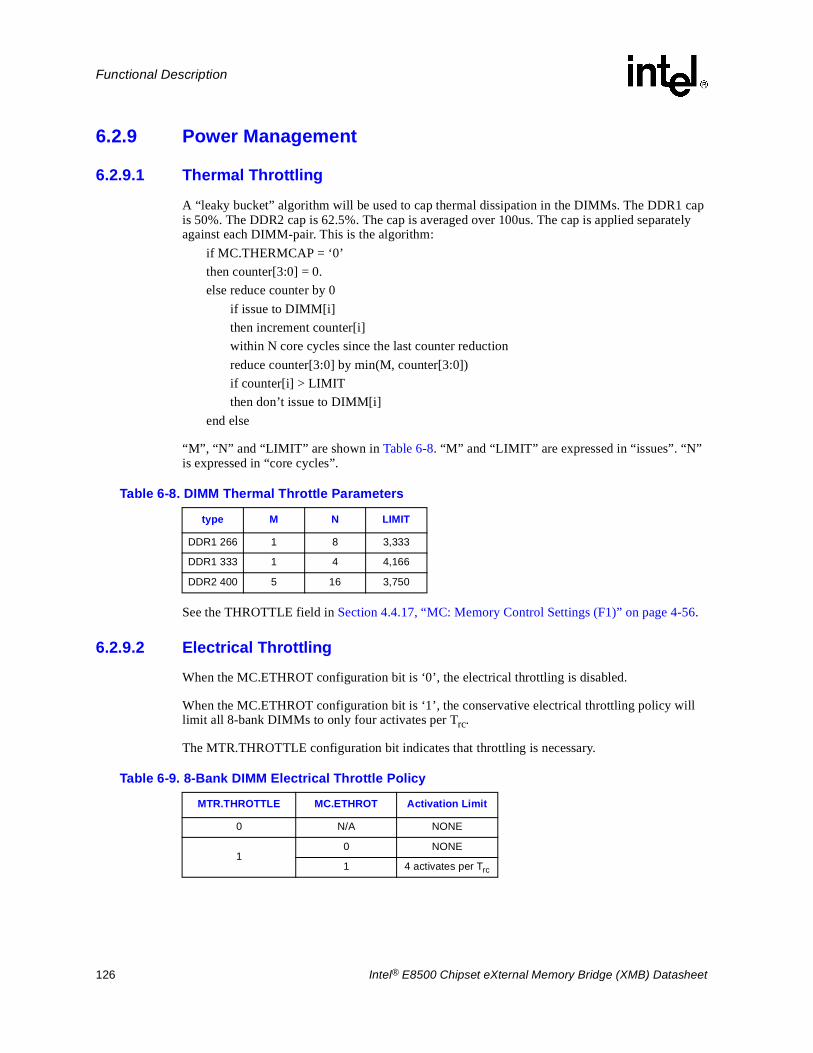
126 Intel® E8500 Chipset eXternal Memory Bridge (XMB) Datasheet
Functional Description
6.2.9 Power Management
6.2.9.1 Thermal Throttling
A “leaky bucket” algorithm will be used to cap thermal dissipation in the DIMMs. The DDR1 cap is 50%. The DDR2 cap is 62.5%. The cap is averaged over 100us. The cap is applied separately against each DIMM-pair. This is the algorithm:
if MC.THERMCAP = ‘0’then counter[3:0] = 0.else reduce counter by 0
if issue to DIMM[i]then increment counter[i]within N core cycles since the last counter reductionreduce counter[3:0] by min(M, counter[3:0])if counter[i] > LIMITthen don’t issue to DIMM[i]
end else
“M”, “N” and “LIMIT” are shown in Table 6-8. “M” and “LIMIT” are expressed in “issues”. “N” is expressed in “core cycles”.
See the THROTTLE field in Section 4.4.17, “MC: Memory Control Settings (F1)” on page 4-56.
6.2.9.2 Electrical Throttling
When the MC.ETHROT configuration bit is ‘0’, the electrical throttling is disabled.
When the MC.ETHROT configuration bit is ‘1’, the conservative electrical throttling policy will limit all 8-bank DIMMs to only four activates per Trc.
The MTR.THROTTLE configuration bit indicates that throttling is necessary.
Table 6-8. DIMM Thermal Throttle Parameters
type M N LIMIT
DDR1 266 1 8 3,333
DDR1 333 1 4 4,166
DDR2 400 5 16 3,750
Table 6-9. 8-Bank DIMM Electrical Throttle Policy
MTR.THROTTLE MC.ETHROT Activation Limit
0 N/A NONE
10 NONE
1 4 activates per Trc

Intel® E8500 Chipset eXternal Memory Bridge (XMB) Datasheet 127
Functional Description
6.3 DDR Channel
6.3.1 Transfer ModeEach DDR SDRAM DIMM is programmed to use a DIMM burst-length of 32 bytes (4 transfers) across each DDR channel. The Mode Register of each SDRAM must be programmed for a burst length of 4, and sequential mode.
6.3.2 Burst OperationThe XMB supports only 32-byte DIMM burst operation on each channel.
Since DDR2 does not support 16-byte burst operation, neither does the XMB support it for DDR1.
6.3.3 Invalid and Unsupported DIMM TransactionsThe XMB does not support or prevent cycle combinations where data interruption or early termination (as defined in the “DDR JEDEC Spec” [1]) would result. Further, the XMB does not prevent or support any combination of transactions that create bus contention (i.e. where multiple DIMMs would be required to drive data simultaneously onto a DDR channel). Also, since the XMB does not support the Burst Stop DDR command, it does not provide a mechanism to interrupt writes for reads. The XMB provides a precharge command, but does not support early read or write termination due to precharge.
6.4 SMBus Port DescriptionThe XMB provides a System Management Bus (SMBus) Revision 2.0 compliant target interface, which provides direct access to all XMB configuration register space. SMBus access is available to all internal configuration registers, regardless of whether the register in question is normally accessed via the memory-mapped mechanism or the standard configuration mechanism. This provides for highly flexible platform management architectures, particularly given a baseboard management controller (BMC) with an integrated network interface controller (NIC) function.
The SMBus interface consists of two interface pins; one a clock, and the other serial data. Multiple initiator and target devices may be electrically present on the same bus. Each target recognizes a start signaling semantic, and recognizes its own 7-bit address to identify pertinent bus traffic. In the XMB, the five most significant bits of the address are hard-coded to 00010b. The 2 least significant bits of the address are strapped to the value of the SMBA1 and SMBA0 pins, respectively.
The protocol allows for traffic to stop in “mid sentence,” requiring all targets to tolerate and properly “clean up” in the event of an access sequence that is abandoned by the initiator prior to normal completion. The XMB is compliant with this requirement.
The protocol includes “wait states” on read and write operations which the XMB takes advantage of to keep the bus busy during internal configuration space accesses.

128 Intel® E8500 Chipset eXternal Memory Bridge (XMB) Datasheet
Functional Description
6.4.1 Internal Access MechanismAll SMBus accesses to internal register space are initiated via a write to the CMD byte. Any register writes received by the XMB while a command is already in progress will receive a NAK to prevent spurious operation. The master is no longer expected to poll the CMD byte to prevent the obliteration of a command in progress prior to issuing further writes. The SMBus access will be delayed by stretching the clock until the data is delivered. Note that per the System Management Bus (SMBus) Specification, Rev 2.0, this can not be longer than 25 ms. To set up an internal access, the four ADDR bytes are programmed followed by a command indicator to execute a read or write. Depending on the type of access, these four bytes indicate either the Bus number, Device, Function, Extended Register Offset, and Register Offset, or the memory-mapped region selected and the address within the region. The configuration type access not only utilizes the traditional bus number, device, function, and register offset, but also uses an extended register offset which expands the addressable register space from 256 bytes to 4 Kbytes. The memory-mapped type access redefines these bytes to be a memory-mapped region selection byte, a filler byte which today is all zeroes, and then the memory address within the region. Note that the filler byte is currently not utilized but enforces that both types of accesses have the same number of address bytes, and allows for future expansion.
It is perfectly legal for an SMBus access to be requested while an IMI-initiated access is already in progress. The XMB supports “wait your turn” arbitration to resolve all collisions and overlaps, such that the access that reaches the configuration ring arbiter first will be serviced first while the conflicting access is held off. An absolute tie at the arbiter will be resolved in favor of the IMI. Note that SMBus accesses must be allowed to proceed even if the internal XMB transaction handling hardware and one or more of the other external XMB interfaces are hung or otherwise unresponsive.
6.4.2 SMBus Transaction Field DefinitionsThe SMBus target port has its own set of fields which the XMB sets when receiving an SMBus transaction. They are not directly accessible by any means for any device.
Table 6-10. SMBus Transaction Field Summary
Position Mnemonic Field Name
Register Mode Memory Mapped Mode
1 CMD Command
2 BYTCNT Byte Count
3 ADDR3 Bus Number Destination Memory
4 ADDR2 Device / Function Number Address Offset [23:16]
5 ADDR1 Extended Register Number Address Offset [15:8]
6 ADDR0 Register Number Address Offset [7:0]
7 DATA3 Fourth Data Byte [31:24]
8 DATA2 Third Data Byte [23:16]
9 DATA1 Second Data Byte [15:8]
10 DATA0 First Data Byte [7:0]
11 STS Status, only for reads

Intel® E8500 Chipset eXternal Memory Bridge (XMB) Datasheet 129
Functional Description
NOTE: Table 6-10 indicates the sequence of data as it is presented on the SMBUS following the byte address of the XMB itself. This is not to necessarily indicate any specific register stack or array implemented in the XMB. Note that the fields can take on different meanings depending on whether it is a configuration or memory-mapped access type. The command indicates how to interpret the bytes.
6.4.2.1 Command Field
The command field indicates the type and size of transfer. All configuration accesses from the SMBus port are initiated by this field. While a command is in progress, all future writes or reads will be NACK’d by the XMB to avoid having registers overwritten while in use. The two command size fields allows for more flexibility on how the data payload is transferred, both internally and externally. The begin and end bits support the breaking of the transaction up into smaller transfers, by defining the start and finish of an overall transfer.
Position Description
7
Begin Transaction Indicator.0 = Current transaction is NOT the first of a read or write sequence.1 = Current transaction is the first of a read or write sequence. On a single transaction sequence
this bit is set along with the End Transaction Indicator.
6
End Transaction Indicator.0 = Current transaction is NOT the last of a read or write sequence.1 = Current transaction is the last of a read or write sequence. On a single transaction sequence
this bit is set along with the Begin Transaction Indicator.
5
Address Mode. Indicates whether memory or configuration space is being accessed in this SMBus sequence.0 = Memory Mapped Mode1 = Configuration Register Mode
4
Packet Error Code (PEC) Enable. When set, each transaction in the sequence ends with an extra CRC byte. The XMB would check for CRC on writes and generate CRC on reads. PEC is not supported by the XMB.0 = Disable1 = Not Supported
3:2
Internal Command Size. All accesses are naturally aligned to the access width. This field specifies the internal command to be issued by the SMBus slave logic to the XMB core.00 = Read Dword01 = Write Byte10 = Write Word11 = Write Dword
1:0
SMBus Command Size. This field specifies the SMBus command to be issued on the SMBus. This field is used as an indication of the length of the transfer so that the slave knows when to expect the PEC packet (if enabled).00 = Byte01 = Word10 = DWord11 = Reserved

130 Intel® E8500 Chipset eXternal Memory Bridge (XMB) Datasheet
Functional Description
6.4.2.2 Byte Count Field
The byte count field indicates the number of bytes following the byte count field when performing a write or when setting up for a read. The byte count is also used when returning data to indicate the following number of bytes (including the status byte) which are returned prior to the data. Note that the byte count is only transmitted for block type accesses on SMBus. SMBus word or byte accesses do not use the byte count.
6.4.2.3 Address Byte 3 Field
This field should be programmed with the Bus Number of the desired configuration register in the lower 5 bits for a configuration access. For a memory-mapped access, this field selects which memory-map region is being accessed. In contrast to how some earlier XMBs operated, there is no status bit to poll to see if a transfer is currently in progress, because by definition if the transfer completed then the task is done. The clock stretch is used to guarantee the transfer is truly complete.
The XMB does not support access to other logical bus numbers via the SMBus port. All registers “attached” to the configuration mechanism SMBus has access to are all on logical bus#0. The XMB makes use of this knowledge to implement a modified usage of the Bus Number register providing access to internal registers outside of the PCI compatible configuration window.
6.4.2.4 Address Byte 2 Field
This field indicates the Device Number & Function Number of the desired configuration register if for a configuration type access, otherwise it should be set to zero.
6.4.2.5 Address Byte 1 Field
This field indicates the upper address bits for the register with the 4K region. Whether it is a configuration or memory-map type of access, only the lower bit positions are utilized, the upper four bits are ignored.
Position Description
7:0 Byte Count. Number of bytes following the byte count for a transaction.
Position Configuration Register Mode Description Memory Mapped Mode Description
7:5 Ignored. Memory map region to access.01h = DMA08h = DDR09h = CHAPOthers = Reserved
4:0Bus Number. Must be zero: the SMBus port can only access devices on the XMB and all devices are bus zero.
Position Configuration Register Mode Description Memory Mapped Mode Description
7:3 Device Number. Can only be devices on the XMB.Zeros used for padding.
2:0 Function Number.
Position Description
7:4 Ignored.
3:0 Extended Register Number. Upper address bits for the 4K region of register offset.

Intel® E8500 Chipset eXternal Memory Bridge (XMB) Datasheet 131
Functional Description
6.4.2.6 Address Byte 0 Field
This field indicates the lower eight address bits for the register with the 4K region, regardless whether it is a configuration or memory-map type of access.
6.4.2.7 Data Field
This field is used to receive read data or to provide write data associated with the desired register.
At the completion of a read command, this field will contain the data retrieved from the selected register. All reads will return an entire aligned DWord (32 bits) of data.
The appropriate number of byte(s) of this 32 bit field should be written with the desired write data prior to issuing a write command. For a byte write only bits 7:0 will be used, for a DWord write only bits 15:0 will be used, and for a DWord write all 32 bits will be used.
6.4.2.8 Status Field
For a read cycle, the data is preceded by a byte of status. The following table shows how these bits are defined.
6.4.3 Unsupported Access AddressesIt is possible for an SMBus master to program an unsupported bit combination into the ADDR registers. The XMB does not support such usage, and may not gracefully terminate such accesses.
Position Description
7:0 Register Offset.
Position Description
31:24 Byte 3 (DATA3). Data bits [31:24] for DWord.23:16 Byte 2 (DATA2). Data bits [23:16] for DWord.
15:8 Byte 1 (DATA1). Data bits [15:8] for DWord and Word.7:0 Byte 0 (DATA0). Data bits [7:0] for DWord, Word and Byte.
Position Description
7Internal Timeout.0 = SMBus request is completed within 2 ms internally1 = SMBus request is not completed in 2 ms internally.
6 Ignored.
5Internal Master Abort.0 = No Internal Master Abort Detected.1 = Detected an Internal Master Abort.
4Internal Target Abort.0 = No Internal Target Abort Detected.1 = Detected an Internal Target Abort.
3:1 Ignored.
0Successful.0 = The last SMBus transaction was not completed successfully.1 = The last SMBus transaction was completed successfully.

132 Intel® E8500 Chipset eXternal Memory Bridge (XMB) Datasheet
Functional Description
6.4.4 SMB Transaction PictogramsSince the new SMB target interface is of enterprise origin, it is more complex than the original SMB target interface of desktop origin. The following figures demonstrate the different types of transactions and how they can be broken up into multiple smaller transfers.
Figure 6-1. DWORD Configuration Read Protocol (SMBus Block Write / Block Read,PEC Disabled)
Figure 6-2. DWORD Configuration Write Protocol (SMBus Block Write, PEC Disabled)
Figure 6-3. DWORD Memory Read Protocol (SMBus Block Write / Bock Read, PEC Disabled)
Figure 6-4. DWORD Memory Write Protocol
Figure 6-5. DWORD Configuration Read Protocol (SMBus Word Write / Word Read,PEC Disabled)
S 0001_0xx W A Cmd = 11000010 ASr 0001_0xx R A Byte Count = 5 A Status A Data[31:24] A Data[23:16] A Data[15:8] A Data[7:0]
S 0001_0xx W A Cmd = 11000010 A Byte Count = 4 A Bus Number A Device/Function A Reg Number[15:0] A
Reg Number [7:0]CLOCK
STRETCH A P
N P
A
S 0001_0xx W A Cmd = 11001110 A Byte Count = 8 A Bus Number A Device/Function A Reg Number[15:8] A Reg Number [7:0] A Data[31:24]
Data[23:16] A Data[16:8] A Data[7:0] CLOCKSTRETCH A P
S 0001_0xx W A Cmd = 11100010 A Byte Count = 4 A Destination Mem A Add Offset[23:16] A Add Offset[15:8] A
S 0001_0xx W A Cmd = 11100010 ASr 0001_0xx R A Byte Count = 5 A Status A Data[31:24] A Data[23:16] A Data[15:8] A Data[7:0] N P
Add Offset[7:0] CLOCKSTRETCH A P
A
S 0001_0xx W A Cmd = 11101110 A Byte Count = 8 A Destination Mem A Add Offset[23:16] A Add Offset[15:8] A Add Ofset[7:0]
Data[23:16] A Data[16:8] A Data[7:0]CLOCK
STRETCH A P
A Data[31:24]
S 0001_0xx W A Cmd = 10000001 A Bus Number A Device/Function
S 0001_0xx W A Cmd = 01000001 A Register Num[15:8]
A P
S 0001_0xx W A Cmd = 10000001Sr 0001_0xx R A Status
S 0001_0xx W A Cmd = 00000001 ASr 0001_0xx R A Data[23:16] A Data[15:8] P
AA Data[31:24] P
A Register Num[7:0] CLOCK STRETCH A P
S 0001_0xx W A Cmd = 01000000 ASr 0001_0xx R A Data[7:0] P
N
N
N

Intel® E8500 Chipset eXternal Memory Bridge (XMB) Datasheet 133
Functional Description
Figure 6-6. DWORD Configuration Write Protocol (SMBus Word Write, PEC Disabled)
Figure 6-7. DWORD Memory Read Protocol (SMBus Word Write / Word Read, PEC Disabled)
Figure 6-8. WORD Configuration Wrote Protocol (SMBus Byte Write, PEC Disabled)
S 0001_0xx W A Cmd = 10001101 A Bus Number A Device/Function
S 0001_0xx W A Cmd = 00001101 A Register Num[15:8]
A P
A Register Num[7:0] A P
CLOCK STRETCH A P
S 0001_0xx W A Cmd = 00001101 A Data[31:24] A Data[23:16] A P
S 0001_0xx W A Cmd = 01001101 A Data[15:8] A Data[7:0]
S 0001_0xx W A Cmd = 10101101 A Dest Mem A Add Offset[23:16]
S 0001_0xx W A Cmd = 00101101 A Add Offset[15:8]
A P
A Add Offset[7:0] A P
CLOCK STRETCH A P
S 0001_0xx W A Cmd = 00101101 A Data[31:24] A Data[23:16] A P
S 0001_0xx W A Cmd = 01101101 A Data[15:8] A Data[7:0]
S 0001_0xx W A Cmd = 01100001 A Add Offset[15:8]
S 0001_0xx W A Cmd = 10100001Sr 0001_0xx R A Status
S 0001_0xx W A Cmd = 00100001 ASr 0001_0xx R A Data[23:16] A Data[15:8] N P
AA Data[31:24] N P
A Add Offset[7:0] CLOCK STRETCH A P
S 0001_0xx W A Cmd = 01100000 ASr 0001_0xx R A Data[7:0] PN
S 0001_0xx W A Cmd = 10001000 A Bus Number
Device/Function
S 0001_0xx W A Cmd = 00001000 A Register Num[15:8]
A P
A P
CLOCK STRETCH A P
S 0001_0xx W A Cmd = 00001000 A Data[W:X] A P
S 0001_0xx W A Cmd = 01001000 A Data[Y:Z]
S 0001_0xx W A Cmd = 00001000 A PA
S 0001_0xx W A Cmd = 00001000 A Register Num[7:0] A P
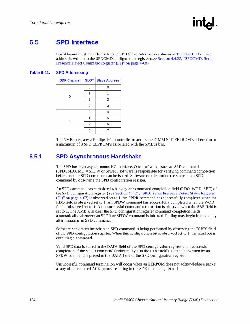
134 Intel® E8500 Chipset eXternal Memory Bridge (XMB) Datasheet
Functional Description
6.5 SPD InterfaceBoard layout must map chip selects to SPD Slave Addresses as shown in Table 6-11. The slave address is written to the SPDCMD configuration register (see Section 4.4.25, “SPDCMD: Serial Presence Detect Command Register (F1)” on page 4-68).
The XMB integrates a Phillips I2C* controller to access the DIMM SPD EEPROM’s. There can be a maximum of 8 SPD EEPROM’s associated with the SMBus bus.
6.5.1 SPD Asynchronous HandshakeThe SPD bus is an asynchronous I2C interface. Once software issues an SPD command (SPDCMD.CMD = SPDW or SPDR), software is responsible for verifying command completion before another SPD command can be issued. Software can determine the status of an SPD command by observing the SPD configuration register.
An SPD command has completed when any one command completion field (RDO, WOD, SBE) of the SPD configuration register (See Section 4.4.24, “SPD: Serial Presence Detect Status Register (F1)” on page 4-67) is observed set to 1. An SPDR command has successfully completed when the RDO field is observed set to 1. An SPDW command has successfully completed when the WOD field is observed set to 1. An unsuccessful command termination is observed when the SBE field is set to 1. The XMB will clear the SPD configuration register command completion fields automatically whenever an SPDR or SPDW command is initiated. Polling may begin immediately after initiating an SPD command.
Software can determine when an SPD command is being performed by observing the BUSY field of the SPD configuration register. When this configuration bit is observed set to 1, the interface is executing a command.
Valid SPD data is stored in the DATA field of the SPD configuration register upon successful completion of the SPDR command (indicated by 1 in the RDO field). Data to be written by an SPDW command is placed in the DATA field of the SPD configuration register.
Unsuccessful command termination will occur when an EERPOM does not acknowledge a packet at any of the required ACK points, resulting in the SDE field being set to 1.
Table 6-11. SPD Addressing
DDR Channel SLOT Slave Address
0
0 0
1 1
2 2
3 3
1
0 4
1 5
2 6
3 7

Intel® E8500 Chipset eXternal Memory Bridge (XMB) Datasheet 135
Functional Description
6.5.2 Clock DividerThe SPD configuration register contains a clock divider field (DIV). With a 1 MHz SPDCLK, Table 6-12 provides the available SPDCLK frequency settings:
6.5.3 SIO Request Packet for SPD Random ReadUpon receiving the SPDR command, the XMB generates the Random Read Register I2C command sequence as shown in Figure 6-9. The returned data is then stored in the XMB SPD configuration register in bits [7:0], and the RDO field is set to ‘1’ by the XMB to indicate that the data is present and that the command has completed without error (see Section 4.4.24, “SPD: Serial Presence Detect Status Register (F1)” on page 4-67).
Table 6-12. SPD.DIV Clock Divider Frequency Table
DIV SPDCLK Frequency (KHz) Frequency Scaler
0 100 10
1 38.5 26
2 23.9 42
3 17.2 58
4 13.5 74
5 11.1 90
6 9.4 106
7 8.2 122
8 7.3 138
9 6.5 154
10 5.9 170
11 5.4 186
12 5 202
13 4.6 218
14 4.3 234
15 4 250
Figure 6-9. Random Byte Read Timing
ACK
SA7
R/
W
C0
C1
C2
SPD0
SPD1
SPD2
SPD3
S
SPD3
SPD2
SACK
SA0
SA1
SA2
SA3
SA4
SA5
SA6
ACK
C0
C1
C2
SPD0
SPD1
NACK
PR/
W
Slave Address Byte Address Slave Address DATA

136 Intel® E8500 Chipset eXternal Memory Bridge (XMB) Datasheet
Functional Description
6.5.4 SIO Request Packet for SPD Byte WriteUpon receiving the SPDW command, the XMB generates the Byte Write Register I2C command sequence as shown in Figure 6-10. The XMB indicates that the SIO command has completed by setting the WOD bit of the SPD configuration register to 1 (see Section 4.4.24, “SPD: Serial Presence Detect Status Register (F1)” on page 4-67).
6.5.5 SPD ProtocolsThe XMB supports the Random Byte Read and Byte Write SMBus protocols.
6.5.6 SPD TimeoutIf there is an error in the transaction, such that the SPD EEPROM does not signal an acknowledge the transaction will time out. The XMB will discard the cycle and set the SBE bit of the SPD configuration register to 1 to indicate this error (see Section 4.4.24, “SPD: Serial Presence Detect Status Register (F1)” on page 4-67). The timeout counter within the XMB begins counting after the last bit of data is transferred to the DIMM, while the XMB waits for a response.
6.5.7 DDR Channel DIMM Data Bit Mapping
6.5.8 DDR DIMM SizingDIMM sizing is performed by using the SPD interface to interrogate the DIMM SPD logic to determine DIMM population and characteristics. The mapping between the DIMM slave address and DIMM chip selects is provided in Table 6-14 and Table 6-11.
Board layout must map chip selects to DIMMs on each DDR channel as shown in Table 6-14.Multiple chip selects per slot indicate opportunity for stacked (dual-rank) DIMMs. Slots accepting dual-rank DIMMs populated with single-rank DIMMs must use the lower (even) chip-selects.
Figure 6-10. Byte Write Register Timing
ACK
SA7
R/
W
C0
C1
C2
SPD0
SPD1
SPD2
SPD3
SACK
SA0
SA1
SA2
SA3
SA4
SA5
SA6
ACK
P
Slave Address Byte Address DATA
Table 6-13. DDR Channel DIMM Data Bit Mapping
DDR Channel DIMM
DQ[63:0] DQ[63:0]
DQ[71:64] CB[7:0]

Intel® E8500 Chipset eXternal Memory Bridge (XMB) Datasheet 137
Functional Description
6.6 Reliability, Availability, and ServiceabilityThe XMB provides data integrity throughout the component. In general the validity of a transaction and data are checked as the transaction is received from the interface.
• Independent Memory Interface (IMI) - the interface uses CRC protection.
• DDR Memory Subsystem - the memory subsystem uses a SDDC algorithm to provide protection across the DIMM Rank. The x8 SDDC will support x8 DRAM devices.
Data entering the write data buffer is protected by CRC12. Data exiting the write data buffer is protected by parity. Inbound data is protected by the same memory SDDC code used in the memory subsystem.
6.6.1 Independent Memory InterfaceThe Independent Memory Interface protects all transfers with a combination packet based CRC and /or SDDC. CRC 12 is used for the outgoing packets. The inbound interface path uses a combination x8 SDDC for data and CRC 8 for link information.
6.6.2 Memory Subsystem Data IntegrityThe XMB will employ a SDDC algorithm for the memory subsystem that will recover from a x8 component failure. The x8 SDDC is a 32-byte two-phase code.
6.6.2.1 Scrubbing
A scrub corrects and logs a correctable memory error, and logs uncorrectable memory errors. A four-byte ECC is attached to each 32-byte “payload”. An error is detected when the 36-bytes read from memory is not a legal code-word. The error is corrected by modifying either the ECC or the payload or both and writing both the ECC and payload back to memory.
Scrubbing will be disabled by default. It will also be disabled during memory test (see Section 6.2.5, “Memory Test and Initialization” ).
Table 6-14. Chip Select Mapping to Available DIMM Slots
SLOTS CS#[0] CS#[1] CS#[2 CS#[3] CS#[4] CS#[5] CS#[6] CS#[7]
4
01
23
3 NC
2 NC
1 NC

138 Intel® E8500 Chipset eXternal Memory Bridge (XMB) Datasheet
Functional Description
6.6.2.2 Patrol Scrubbing
To enable this function, the XMBCFGNS.SCRBEN configuration bit must be set.
The scrub unit starts at DIMM Rank 0 / Address 0 upon reset. Every 16k core cycles the unit will scrub one cache line and then increment the address one cache line. Using this method, roughly 64GBytes of memory behind the XMB can be completely scrubbed every day.
Error logs include RAS/CAS/BANK/RANK and x8 device location for a correctable error.
6.6.2.3 Normal
This patrol-scrub mode is in effect when the MC.PSCRBALGO configuration bit is cleared. This setting is appropriate when the memory is solely composed of x4 DRAMs.
An erroneous read will be logged and re-read. If the re-read is correctable, it is corrected (scrubbed) in memory. A conflicting read or write request pending issue will be held until the scrub is finished.
6.6.2.4 Enhanced
This patrol-scrub mode is in effect when the MC.PSCRBALGO configuration bit is set. This setting is appropriate when the memory contains any x8 DRAMs.
This mode checks for aliasing errors (see the Demand Scrubbing section below for an explanation). A correctable read that is determined to be a possible alias is logged as an uncorrectable, and a correctable re-read that is determined to be a possible alias is not corrected.
6.6.2.5 Demand Scrubbing
To enable this function, the MC.DEMSEN configuration bit must be set.
Erroneous read data will be returned to the IMI. Error logs include RAS/CAS/BANK/RANK and x8 device location for a correctable error.
6.6.2.6 Normal
This demand-scrub mode is in effect when the MC.SCRBALGO configuration bit is cleared. This setting is appropriate when the memory is solely composed of x4 DRAMs.
An erroneous read is logged. If it was correctable, it is re-read. If the re-read is correctable, it is corrected (scrubbed) in memory. A conflicting read or write request pending issue after the re-read will be held until the scrub is either completed or aborted (because the re-read was not correctable).

Intel® E8500 Chipset eXternal Memory Bridge (XMB) Datasheet 139
Functional Description
6.6.2.7 Enhanced
This demand-scrub mode is in effect when the MC.SCRBALGO configuration bit is set. This setting is appropriate when the memory contains any x8 DRAMs.
if the first read had an uncorrectable errorthen log an uncorrectable error
if the first read had a correctable errorthen....log a correctable error
....if a different bad device had been previously marked in the same rank as the first read and
........the weight of one of the symbols of the first read was greater than zero and
........the weight of the other symbol of the first read was greater than zero
....then log fatal error X21
....else
........issue a second read
........if the second read had an uncorrectable error
........then log fatal error X21
........if the second read had a correctable error
........then correct (scrub) it in memory
....... if the second read was correctable and the weight of one of the symbols of the first read was greater than zero and the weight of the other symbol of the first read was greater than zero....... then
...........issue a third read
............if the third read was correctable with errors in both symbols
............then mark the bad device in the BADRAM{A/B} configuration register
............if the third read had an uncorrectable error
............then log fatal error X21
........end if
....end if
end if
A conflicting read or write request pending issue after the second read will be held until the scrub is either completed or aborted (because the second read was not correctable).

140 Intel® E8500 Chipset eXternal Memory Bridge (XMB) Datasheet
Functional Description
6.6.2.8 Normal DIMM Sparing
At configuration time, a DIMM rank is set aside to replace a defective DIMM rank. When the error rate for a failing DIMM rank reaches a pre-determined threshold, the MS.LBTHR configuration bit is set the XMB will issue an “interrupt” in-band IMI signal and initiate a spare copy. While the copy engine is line-atomically reading locations from the failing DIMM rank and writing them to the spare, system reads will be serviced from the failing DIMM rank, and system writes will be written to both the failing DIMM rank and the spare DIMM rank.
An erroneous copy read will be logged appropriately. If correctable, it is corrected (scrubbed) in the spare rank. If uncorrectable, it is poisoned in the spare rank.
If the MC.SSCRBALGO configuration bit is set, correctable errors that are regarded as possible aliases (see Demand Scrubbing for an explanation), are logged as uncorrectable and poisoned in the spare rank.
A conflicting read or write request pending issue after the re-read will be held until the line is either scrubbed or poisoned.
At the completion of the copy, the failing DIMM rank is disabled and the “spared” DIMM rank will be used in its place. The XMB will change the rank numbers in the DMIRs from the failing rank to the spare rank.
This mechanism requires no software support once it has been enabled by designating the spare rank through the MC.SPRANK configuration register field and enabling sparing by setting the DRT.SPAREN configuration bit. Hardware will detect the threshold-initiated fail-over, accomplish the copy, and off-line the “failed” DIMM rank once the copy has completed. This is accomplished autonomously by the memory control subsystem. The MS.SFO configuration bit is set and an “interrupt” in-band IMI signal is issued indicating that a sparing event has completed.
6.6.2.9 Failure Rate Algorithm
The XMB tracks the number of failures per DIMM Rank. The failure rate per rank will be tracked for both correctable and uncorrectable errors. The method to track the error rate will employ a leaky bucket algorithm.
The failure rate target is programmable for the XMB and has two components to the calculations. These are as follows:
• Failure count at which the copy engine is enabled to copy the image from the failing DIMM Rank to the spare. The failure count is programmable from 1 to 15 in the MC.SETH configuration register field.
• Rate at which the count will be decremented (see Section 4.4.43, “ERRPER: ERROR Period” on page 80). There is one free-running error period timer per XMB. At a core frequency of down to 166 MHz this provides the ability to have “drip” out of the bucket at a highly granular programmable rate with periods up to 16 days. The 32-bit error period counter leverages a 16-bit pre-scalar.
Each DIMM rank has two 4-bit error counters, one counter for correctable errors and the other for uncorrectable errors (see Section 4.4.41, “UERRCNT: Uncorrectable Error Count (F1)” on page 4-78 and Section 4.4.42, “CERRCNT: Correctable Error Count (F1)” on page 4-79).
• When an error is detected the appropriate counter is iterated.

Intel® E8500 Chipset eXternal Memory Bridge (XMB) Datasheet 141
Functional Description
• When the error period counter reaches a terminal count and the error counter is non-zero and the error counter is not frozen, then the error counter is decremented.
• When an error counter reaches its threshold then the sparing copy engine is enabled to copy the memory image from the failing to the spare rank.
6.6.2.10 XMB Copy Engine
The copy engine is enabled by the “Spare Control Enable” bit in Section 4.4.23, “DRC: DRAM Controller Mode Register (F1)” on page 4-65.
The XMB copy engine will be passed which DIMM rank to read (the rank that has reached threshold in the UERRCNT or CERRCNT configuration register) and which DIMM rank to write (the rank designated by the MC.SPRANK configuration register field, See Section 4.4.17, “MC: Memory Control Settings (F1)” on page 4-56). The copy engine will start at DIMM address “0” of the DIMM rank. It will read from the failing rank, and write to the spare rank.
An erroneous copy read will be logged appropriately and re-read from the failing rank. If the re-read is correctable, it is corrected (scrubbed) in the spare rank. If the re-read is uncorrectable, it is poisoned in the spare rank.
A conflicting read or write request pending issue after the re-read will be held until the line is either scrubbed or poisoned.
During this time all IMI writes destined to the failing DIMM are written to both DIMMs. At the completion of the copy the spare will become the operational rank after it has been refreshed. It should be noted that if the spare rank is larger, locations not covered by the DMIR.LIMIT’s are unusable.
The length of the copy is defined by the minimum size of either the spare or the failing DIMM rank.
During copy, system accesses will be allocated 8 out of 10 DDR_CLK’s available for memory issue. The copy engine will absorb 2 out of every 10 consecutive DDR_CLK’s available for memory issue. The following “parasitic” processes absorb DDR_CLK’s unavailable for memory issue:
• Thermal throttles
• Electrical throttles
• Patrol scrubs
• Demand scrubs
• Refreshes
It is possible for the copy engine to “wipe” the failing DIMM rank locations. This can be defined by the WIPE configuration bit described in Section 4.4.17, “MC: Memory Control Settings (F1)” on page 4-56. The length of the wipe is the size of the failing DIMM rank.

142 Intel® E8500 Chipset eXternal Memory Bridge (XMB) Datasheet
Functional Description
6.6.2.11 Zero-Overhead Sparing
The XMB supports zero-overhead sparing. After graceful degradation has de-allocated memory, a larger, equal, or smaller spare DIMM rank which has been “freed up” by de-allocation can be designated by software to replace a failing DIMM rank. The copy operation is identical to DIMM sparing with the following exceptions:
• MC.SPRANK is not designated until memory has been de-allocated.
• DRC.SPAREN is not set until MC.SPRANK has been designated.
• One and only one UERRCNT / CERRCNT count should be at threshold. Hardware will not commence a spare copy if multiple error counts are at threshold.
6.6.3 Error ReportingThe error reporting for the XMB is comprised of the status (FERR and NERR configuration registers), error log (recoverable and nonrecoverable configuration registers), and the error signaling mechanism over the IMI interface.
6.6.3.1 Error Status and Log Configuration Registers
Error status configuration registers are provided: FERR (first error status register), and NERR (Next & Subsequent error status register). First fatal and/or first non-fatal errors are flagged in the FERR configuration register. Subsequent errors are indicated in the NERR configuration register. Associated with some of the errors flagged in the FERR configuration register are control and data logs. The IMI logging configuration registers are RECIMI and RECXCFG.
The contents of FERR and NERR are “sticky” across a reset (while PWRGOOD remains asserted). This provides the ability for firmware to perform diagnostics across reboots. Note that only the contents of FERR affects the update of the error log configuration registers.
Table 6-15. Errors Detected by the XMB (Sheet 1 of 3)
ERR# Error Name ErrorType
Log Register Cause / Actions
Memory Interface Errors
IMI1 Outbound CRC Error Corr RECIMI XMB must flush any write packet currently in progress. XMB throws away data packets and re-aligns on the next write header.
IMI2 NA
IMI3 NA
IMI4 NA
IMI5 Too many write data packets Corr N/AXMB must flush any write packet currently in progress. XMB throws away data packets and re-aligns on the next write header.
IMI6 NA
IMI7 NA
IMI8 Un-implemented Command Error Corr RECIMI XMB will signal a Corr. Error and log error. XMB must provide a NACK response.

Intel® E8500 Chipset eXternal Memory Bridge (XMB) Datasheet 143
Functional Description
IMI9 Too few write data packets Corr N/AXMB must flush any write packet currently in progress. XMB throws away data packets and re-aligns on the next write header.
IM10
Memory write data poisoned. TheNB has poisoned the packet that contains the error and written the data to memory
Corr N/A XMB will poison the 32 byte codeword in memory.
IMI11 NA
IMI12 Read Request Overflow Corr RECMEM(A/B)
XMB aborted read that overflowed read request queue. Log that event occurred (XMB and NB).
IMI13 Command Throttle Limit Exceeded UnCorr N/A Log that event occurred (XMB).
IMI14 Rejected IMI write to “RRW” attributed registers Corr RECXCFG Log that event occurred.
IMI15 NA
IMI16 NA
IMI17 NA
IMI18
Config write data poisoned. The NB has poisoned the packet that contains the error and written the data to config.
Corr RECXCFG XMB will drop and NACK. Update RECXCFG with the access that was dropped.
XMB and Memory Subsystem
X1 Correctable Data ECC Error (Request) Corr
RECMEM(A/B)&
REDMEM((if XMB not
secure)
Reread location and fix if still in error.Note to software: check CERRCNT to determine error threshold reached.
X2Multi-bit Data ECC Error (Request)(Do not Include Poisoned Data)
UnCorr
RECMEM(A/B &
REDMEM((if XMB not
secure)
Reread location and fix if correctable else leave as is in memory.Note to software: check UERRCNT to determine error threshold reached.
X3 Correctable Patrol Scrub Error Corr
RECMEM(A/B &
REDMEM((if XMB not
secure)
Reread location and fix if still in error.
X4Multi-bit Data ECC Error (Scrub)(Do not Include Poisoned Data)
Corr
RECMEM(A/B &
REDMEM((if XMB not
secure)
Reread location and fix if correctable else leave as is in memory.
X5 N/A N/A N/A N/A
X6 N/A N/A N/A N/A
X7 N/A N/A N/A N/A
X8 SPD Error (protocol) Corr N/A XMB to log/signal the error occurred.
X9 Write Post Buffer Parity Error Fatal RECMEM(A/B
Previously Posted Write is corrupted by XMB. XMB Functionality has been compromised.
Table 6-15. Errors Detected by the XMB (Sheet 2 of 3)
ERR# Error Name Error Type
Log Register Cause / Actions

144 Intel® E8500 Chipset eXternal Memory Bridge (XMB) Datasheet
Functional Description
6.6.3.2 Error Logs
For some errors, control and/or data logs are provided. The “non-recoverable” error logs are used to log information associated with first fatal errors. The “recoverable” error logs are used for first correctable and uncorrectable errors.
Once a first error for a type (fatal, correctable, uncorrectable) of error has been flagged (and logged), the log configuration registers for that error type remain fixed until either 1) any errors in the FERR configuration register for which the log is valid are cleared or 2) a power-on or PWRGOOD reset.
6.6.3.3 Error Signaling
Associated with each of the FERR/NERR configuration registers are signal codes over the IMI port to signal to the NB that an error has occurred. If not masked (EMASK configuration register), this signal will reflect the error status of the XMB.
The signal mechanism for communicating asynchronous signals from the XMB to the NB is in the IMI inbound link layer control information. Valid signal codes used by the XMB include:
• 3 virtual signals for error notification, these being, FATAL, Uncorrectable Error, and Correctable Error.
• 2 virtual signals for actions, these being MCERROR and ICHRST.
X10 UnCorrectable Data Error during DIMM Sparing Function Corr RECMEM(A
/BDuring Sparing Copy, the engine had to poison a location in the spare DIMM.
X11 Correctable Data Error during DIMM Sparing Function Corr RECMEM(A
/BDuring Sparing Copy, the engine had to correct data location in the spare DIMM.
X12 Out of Range Access (Read/Write) Corr RECMEM(A/B Capture Requesting Address.
X13 Write Buffer Overflow Corr RECMEM(A/B Drop Writes and Log the Address.
X14 N/A N/A N/A N/A
X15 N/A N/A N/A N/A
X16 Memory Test Mismatch Corr MTSTAT Indicate mismatching DIMM in MTSTAT.
X17 More than one IMI Config Command Outstanding Corr RECXCFG Log that event occurred. Abort transaction.
X18 N/A N/A N/A N/A
X19 N/A N/A N/A N/A
X20 N/A N/A N/A N/A
X21 Detected Aliased Device + SBE uncorrectable error Fatal RECMEM(A
/B Log Address.
X22 Received a Memory Request during memory initialization Corr RECMEM(A
/B Issue NAK response, drop request.
Table 6-15. Errors Detected by the XMB (Sheet 3 of 3)
ERR# Error Name ErrorType
Log Register Cause / Actions

Intel® E8500 Chipset eXternal Memory Bridge (XMB) Datasheet 145
Functional Description
6.6.3.4 Errors and Resets
Spurious errors are not recorded during reset. No error is captured (or later signaled over the IMI port) due-to or during-a reset.
6.7 Clocking
6.7.1 Reference ClocksThe IMI_CLK reference clock, operating 167 MHz, is supplied to the XMB. This is the IMI and Core PLLs’ reference clock. The clock frequency is common to both IMI agents (NB and XMB), but no phase matching between them is required to achieve optimum performance.
Synchronous clock gearing is employed between the IMI and the core. However, synchronous subsystems must scale across frequency sweeps at the same gear ratios chosen for nominal operation (that includes the core, IMI, and DDR). The JTAG asynchronous subsystem need not scale. The gear ratios are shown in Table 6-16.
6.7.2 RAM Clocking SupportThe DDR command clocks (DDR_{A,B}_CLK, DDR_{A,B}_CLK#) are generated by the DDR PLL. They operate at 1/2X the core frequency for 266 MHz DDR1, and at 1X the core frequency for 333 MHz DDR1 and 400MHz DDR2. The write strobes operate at the same frequency as DDR_CLK. Write data and check bits are aligned to both the rising and falling edges of the write strobe.
The source-synchronous read strobes operate at the same rates as the write strobes. Each read strobe will be individually aligned with its portion of the data and check bits.
6.7.3 JTAGTCK is asynchronous to the core clock. For private TAP configuration register accesses, one TCK cycle is a minimum of 10 core cycles. The TCK high time is a minimum of 5 core cycles in duration. The TCK low time is a minimum of 5 core cycles in duration. The possibility of metastability during private configuration register access is mitigated by circuit design. A metastability hardened synchronizer will guarantee an MTBF greater than 107 years.
For public TAP configuration register accesses, TCK operates independently of the core clock.
Table 6-16. XMB Gear Ratios
IMI Frequency DDR Frequency Core Frequency IMI: Core Core : DDR
2.67GHz 266 MHz 266MHz 10 : 1 1 : 1
2.67GHz 333 MHz 167 MHz 16 : 1 1 : 2
2.67GHz 400 MHz 200MHz 40 : 3 1 : 2

146 Intel® E8500 Chipset eXternal Memory Bridge (XMB) Datasheet
Functional Description
6.7.4 SMBusThe SMBus clock is synchronized to the core clock. Data is driven into the XMB with respect to the serial clock signal. Data received on the data signal with respect to the clock signal will be synchronized to the core using a metastability hardened synchronizer guaranteeing an MTBF greater than 107 years. The serial clock can not be active until 10 mS after RST## de-assertion. When inactive, the serial clock should be deasserted (High). The serial clock frequency is 100 KHz.
6.7.5 Serial Presence DetectThe transmitted 100 KHz serial presence detect clock is derived from the core clock.
6.7.6 Clock Pins
6.7.7 High-Frequency Clocking Support
6.7.7.1 Power-on Defaults
The core and DDR domains support 266-MHz DDR operation at power-up. These domains can be re-programmed through the DDRSPD configuration register to support DDR 333 and DDR2 400 frequencies by a hard re-sync reset.
Table 6-17. Clock Pins and PLL Power Pins
Pin Name Pin Description
IMI_CLKP IMI clock
IMI_CLKN IMI clock (Complement)
VCCA_IMI[1:0] analog power supply for IMI PLL
VSSA_IMI[1:0] analog ground for IMI PLL
VCCA analog power supply for Core PLL
VSSA analog ground for Core PLL
TCK XDP clock
SPDCLK DIMM serial presence detect I2C clock
SMBCLK SMBus clock
XDP_DSTBP Debug bus strobe
XDP_DSTBN Debug bus strobe (Complement)
DDR_{A,B}_CLK[3:0] DDR clocks
DDR_{A,B}_CLK[3:0]# DDR clocks (Complements)
DDR_{A,B}_DQS[17:0] DDR data strobes
DDR_{A,B}_DQS[17:0]# DDR data strobes (Complements)

Intel® E8500 Chipset eXternal Memory Bridge (XMB) Datasheet 147
Functional Description
6.7.7.2 Spread Spectrum Support
The XMB PLL will support Spread Spectrum Clocking (SSC). SSC is a frequency modulation technique for EMI reduction. Instead of maintaining a constant frequency, SSC modulates the clock frequency/period along a predetermined path (i.e. the modulation profile).The XMB is designed to support a nominal modulation frequency of 30 kHz with a downspread percentage of 0.5%.
6.7.7.3 Stop Clock
The PLLs in the XMB cannot be stopped.
6.7.7.4 Jitter
The IMI clock is produced by a PLL that multiplies the IMI_CLK frequency by 16x. The multi-GHz clock requires an ultra-clean source, ruling out all but specifically crafted low-jitter clock synthesizers.
Strong recommendation: IMI_CLK cycle-to-cycle jitter delivered to the package ball should be less than or equal to 50ps (±25ps). HCLKIN cycle-to-cycle jitter delivered to the package ball must be less than 150ps (±75ps).
6.7.7.5 PLL Lock Time
All PLLs should lock within 1 mS of PWRGOOD signal assertion or hard re-sync RST# signal assertion. The reference clocks must be stable on the assertion of PWRGOOD. The assertion of the PWRGOOD or hard re-sync RST# signal initiates the PLL lock process. External clocks dependent on PLLs are DDR clocks and strobes, serial presence detect clock, and SMBus clock. Many JTAG private configuration registers are dependent on core PLL-generated clocks.
6.8 Reset
6.8.1 Reset Types and TriggersTable 6-18 shows the different types of reset supported by the XMB and the trigger to achieve each type.
Table 6-18. Reset Types and Triggers (Sheet 1 of 2)
Type Trigger
Power-up Core power supply energized
Power Good PWRGOOD de-asserted
Re-syncRST# asserted with DDRFRQ.NEXT != DDRFRQ>NOW

148 Intel® E8500 Chipset eXternal Memory Bridge (XMB) Datasheet
Functional Description
6.8.2 Reset ControlResetting of the XMB chip is directly controlled by four input signals. PWRGOOD indicates when power (and reference clock) are stable. RST# allows the NB.IMI to reset the XMB. The IMI_FRAME pad is used to reset the XMB in a repeatable fashion. TRST# resets the JTAG logic which runs on TCLK. Additional details about these signals are given below.
6.8.2.1 PWRGOOD
The board should hold the PWRGOOD low until power and reference clock have stabilized. This resets most of the chip to a safe initial state. The PLLs and TAP are not reset. When PWRGOOD goes high, logic resets the main PLL and waits for RST# to be deasserted. Before power goes away, PWRGOOD should be pulled low.
6.8.2.2 IMI_RESET#
This active low signal is driven by the NB.IMI end of the IMI bus. It must be asserted (driven low) while PWRGOOD is low and can be deasserted after the main XMB PLL has finished resetting. Whenever the NB.IMI wants to reset the XMB, it de-asserts and then reasserts this signal.
6.8.2.3 IMI_FRAME
This signal allows the IMI.NB to reset the XMB in a repeatable fashion. If the NB.IMI drives IMI_FRAME with a framing signal, the XMB will reset itself in a predictable way relative to the framing signal. This allows the NB.IMI and XMB to behave repeatably after a reset.
6.8.2.4 TRST#
This active low signal resets the logic which runs on TCLK. This includes the TAP, boundary scan ring and some other JTAG scan rings. In a normal system, this input should either be pulled low or connected to PWRGOOD.
6.8.3 Reset SequencesThe PWRGOOD, RST# and TRST# signals all start out low. This causes all internal resets to be asserted.
After power comes up and IMI_CLK stabilizes, the PLLs start generating clocks. At this time, the phase relations between the clocks are not guaranteed to be correct.
IMIRST# asserted with DDRFRQ.NEXT = DDRFRQ>NOW
JTAG XDP_TRST# assertion or reset command though JTAG protocol:
SMBus Reset command though SMBus
Table 6-18. Reset Types and Triggers (Sheet 2 of 2)
Type Trigger

Intel® E8500 Chipset eXternal Memory Bridge (XMB) Datasheet 149
Functional Description
PWRGOOD rises. This releases the reset on the logic running on IMI_CLK. The chip waits until for between 2.5 and 4.0 uS max. PWRGOOD must remain stable during this time. If it falls, the wait starts again until a stable high occurs.
The chip starts looking at IMI_FRAME to bring the internal clocks into alignment with the IMI_FRAME signal.
At this point, the chip waits for RST# to rise. When it does, the internal resets are deasserted for all clock domains except TCLK.
6.8.4 Reset Sequence for a Normal IMI ResetThe chip is running with the PWRGOOD and RST# signals both high.
The NB.IMI drops the RST# signal indicating that it wants to reset the chip.
The memory controller shuts itself down and indicates that it is ready for reset.
Reset is asserted for all “not sticky” registers.
The PLL remains in lock. To guarantee repeatable operation a GO bit must appear on IMI_FRAME. This will reset the PLL to bring the internal clocks into alignment with the IMI_FRAME signal.
At this point, the chip waits for RST# to rise. When it does, the internal resets are deasserted for all clock domains except TCLK.
6.8.5 Reset Sequence for a Resync IMI ResetThe chip is running with the PWRGOOD and RST# signals both high.
The IMI.NB drops the RST# signal indicating that it wants to reset the chip.
The memory controller shuts itself down and indicates that it is ready for reset.
DDRFRQ.NOW and DDRFRQ.NEXT are different so a frequency change will occur.
Reset is asserted for all “sticky” and “not sticky” registers. Reset is not asserted for “extra sticky” registers.
DDRFRQ.NOW is updated from DDRFRQ.NEXT. This changes the PLL configuration bits, and may cause the PLL to lose lock. The chip waits from 2.5 to 4.0 uS to assure that the PLL has re-locked.
To guarantee repeatable operation a GO bit must appear on IMI_FRAME after the PLL has re-locked. This will reset the PLL to bring the internal clocks into alignment with the IMI_FRAME signal.
At this point, the chip waits for RST# to rise. When it does, the internal resets are deasserted for all clock domains except TCLK.

150 Intel® E8500 Chipset eXternal Memory Bridge (XMB) Datasheet
Functional Description
6.8.6 JTAG ResetsVarious resets affect various areas of the JTAG circuitry. This is summarized in the following table
:
6.8.7 SMB ResetsThe SMB protocol includes resets which reset the state of the SMB controller. SMB resets have no effect on the rest of the XMB.
§
Table 6-1. JTAG Resets
JTAGArea
Reset by:
PowerGood Reset(PWRGOOD = 0)
IMI Reset(RESET# = 0)
Test Reset(TRST# = 0)
TAP Reset(TMS = 1 for
5 TCLK cycles)
TAPController - - Yes Yes
BoundaryScanChain
- - - -
Chainsclocked by
t_clk- - Yes -
Chainsclocked by
core_clkYes Yes - -

Intel® E8500 Chipset eXternal Memory Bridge (XMB) Datasheet 151
7 Ballout/Pinout and Package Information
7.1 Intel® E8500 Chipset eXternal Memory Bridge (XMB) Ballout and PinoutThe XMB ballout documents the location of the signals on the package for the two DDR/DDR2 memory channels, the Independent Memory Interface (IMI), and the various power, ground, and reference pins.
Figure 7-1. XMB Ballout (Top View)
AGAFAEADACABAA
YWVUTRPNMLKJHGFEDCBA
12
34
56
78
910
1112
1314
1516
1718
1920
2122
2324
2526
27
IMI
DDR/DDR2A & B
2829
12
34
56
78
910
1112
1314
1516
1718
1920
2122
2324
2526
2728
29
AJAH
AGAFAEADACABAAYWVUTRPNMLKJHGFEDCBA
AJAH
CoreVoltage

152 Intel® E8500 Chipset eXternal Memory Bridge (XMB) Datasheet
Ballout/Pinout and Package Information
Figure 7-2. XMB Ballout with Signal Names (Top View - Left Region)
1 2 3 4 5 6 7 8 9 10 11 12 13 14 15
A0 0 P2V5 /
P1V8DDR_B_M
A6 VSS DDR_B_CB4 VSS DDR_B_D
QS17P2V5 / P1V8
DDR_B_CB6 VSS DDR_A_CL
K0 VSS DDR_A_CLK2
P2V5 / P1V8
A
B0 VSS DDR_B_M
A7DDR_B_M
A5DDR_B_M
A4DDR_B_M
A3DDR_B_CB
5DDR_B_CB
0DDR_B_D
QS17#DDR_B_D
QS8#DDR_B_CB
7DDR_B_CB
3DDR_A_CL
K0#DDR_A_CL
K3DDR_A_CL
K2# B
CVSS DDR_B_M
A9DDR_B_M
A11DDR_B_M
A8P2V5 / P1V8
DDR_B_MA2 VSS DDR_B_CB
1 VSS DDR_B_DQS8
P2V5 / P1V8
DDR_B_CB2 VSS DDR_A_CL
K3# VSSC
D
DDR_A_MA1 VSS DDR_B_M
A12DDR_B_M
A14 VSS DDR_B_DQ30
DDR_B_MA1 VSS DDR_B_D
Q26DDR_B_D
Q31DDR_B_D
Q27 VSS DDR_A_CLK1
DDR_A_CLK1# VSS
D
E
DDR_A_MA2
DDR_B_CKE0
P2V5 / P1V8
DDR_B_BA2
DDR_B_DQ25
P2V5 / P1V8
DDR_B_DQS3#
DDR_B_DQS3
P2V5 / P1V8
DDR_A_DQ30 VSS DDR_A_CB
4P2V5 / P1V8
DDR_B_CLK3#
DDR_B_CLK3 E
F
P2V5 / P1V8
DDR_B_CKE1
DDR_B_DQ19 VSS DDR_A_DQ
29DDR_A_DQ
25 VSS DDR_B_DQS12
DDR_B_DQS12# VSS DDR_A_DQ
26P2V5 / P1V8
DDR_A_DQS17 VSS RESERVED
F
G
DDR_A_MA3 VSS DDR_B_D
Q23DDR_B_D
Q18 VSS DDR_B_DQ24
DDR_A_DQ24 VSS DDR_B_D
Q29DDR_B_D
Q28 VSS DDR_A_CB6
DDR_A_DQS17#
DDR_A_DQS8# VSS
G
H
DDR_A_MA4
DDR_B_DQ22 VSS DDR_A_DQ
18DDR_A_DQ
23P2V5 / P1V8
DDR_A_DQ19
DDR_A_DQS12#
P2V5 / P1V8
DDR_A_DQ31
DDR_A_DQ27 VSS P2V5 /
P1V8DDR_A_DQ
S8DDR_A_CB
0 H
JVSS DDR_B_D
QS2DDR_B_D
QS2#P2V5 / P1V8
DDR_A_DQ22
DDR_A_DQS2 VSS DDR_A_DQ
S12DDR_A_DQ
S3 VSS DDR_A_DQ28
DDR_A_CB5
DDR_A_CB1 VSS DDR_A_CB
7 J
K
DDR_A_MA5
P2V5 / P1V8
DDR_B_DQS11#
DDR_B_DQS11 VSS DDR_A_DQ
S11#DDR_A_DQ
S2# VSS DDR_A_DQS3# VSS P2V5 /
P1V8 RESERVED VSS VSS VSSK
L
DDR_A_MA6
DDR_B_DQ17 VSS DDR_B_D
Q21DDR_A_DQ
S11 VSS DDR_A_DQ17
XDP_DSTBP
P2V5 / P1V8 VSS P1V5 VSS P1V5 VSS P1V5
L
MVSS DDR_B_D
Q16DDR_B_D
Q20 VSS DDR_A_DQ21
DDR_A_DQ16
P2V5 / P1V8
XDP_DSTBN XDP_D8# P1V5 VSS P1V5 VSS P1V5 VSS
M
N
DDR_A_MA8
P2V5 / P1V8
DDR_B_DQ11
DDR_B_DQ10
P2V5 / P1V8
DDR_A_DQ20
DDR_A_DQ11 VSS XDP_D0# VSS P1V5 VSS P1V5 VSS P1V5
N
P
DDR_A_MA7
DDR_B_DQ15 VSS DDR_B_D
Q14DDR_A_DQ
10 VSS DDR_A_DQ15 XDP_D9# XDP_D1# P1V5 VSS P1V5 VSS P1V5 VSS
P
R
P2V5 / P1V8
DDR_B_DQS1
DDR_B_DQS1# VSS DDR_A_DQ
14DDR_A_DQ
S1 VSS XDP_D10# XDP_D2# VSS P1V5 VSS P1V5 VSS P1V5R
T
DDR_A_MA11 VSS DDR_B_D
QS10#DDR_B_D
QS10P2V5 / P1V8
DDR_A_DQS10#
DDR_A_DQS1# XDP_D11# XDP_D3# P1V5 VSS P1V5 VSS P1V5 VSS
T
U
DDR_A_MA9
DDR_B_DQ9 VSS DDR_B_D
Q13DDR_A_DQ
S10 VSS DDR_A_DQ9 XDP_D12# XDP_D4# VSS P1V5 VSS P1V5 VSS P1V5
U
VVSS DDR_B_D
Q12DDR_B_D
Q8P2V5 / P1V8
DDR_A_DQ13
DDR_A_DQ12 VSS XDP_D13# XDP_D5# P1V5 VSS P1V5 VSS P1V5 VSS
V
W
DDR_A_MA12
P2V5 / P1V8
DDR_B_DQ3
DDR_B_DQ7 VSS DDR_A_DQ
8DDR_A_DQ
3 XDP_D14# XDP_D6# VSS P1V5 VSS P1V5 VSS P1V5W
Y
DDR_A_BA2
DDR_B_DQ2 VSS DDR_B_D
Q6DDR_A_DQ
7P2V5 / P1V8
DDR_A_DQ2 XDP_D15# XDP_D7# P1V5 VSS P1V5 VSS P1V5 VSS
Y
AA
P2V5 / P1V8
DDR_B_DQS0
DDR_B_DQS0# VSS DDR_A_DQ
6DDR_A_DQ
S0 VSS RST# PWRGOOD TESTLO IMI_FRAME VSS TETSHI TESTLO VSS
AA
AB
DDR_A_MA14 VSS DDR_B_D
QS9#DDR_B_D
QS9P2V5 / P1V8
DDR_A_DQS0# RESERVED TESTLO TESTHI VSS P1V5 VSS VSS VSS VSS
AB
AC
DDR_A_CKE0
DDR_B_DQ1 VSS DDR_B_D
Q5DDR_A_DQ
S9# VSS VSS P1V5 IMI_TXP15 IMI_TXN15 VSS IMI_RXP9 IMI_RXN9 P1V5 IMI_RXP6AC
ADVSS DDR_B_D
Q0DDR_B_D
Q4P2V5 / P1V8
DDR_A_DQS9 VSS IMI_LINKP
1IMI_LINKN
1 VSS IMI_TXP13 IMI_TXN13 P1V5 IMI_RXP8 IMI_RXN8 VSSAD
AE
DDR_A_CKE1 VSS DDR_A_DQ
5DDR_A_DQ
1 VSS P1V5 VSS IMI_TXP17 IMI_TXN17 P1V5 IMI_TXP11 IMI_TXN11 VSS IMI_RXP7 IMI_RXN7AE
AF
DDR_B_VREF
DDR_A_DQ4
DDR_A_DQ0 VSS VSS IMI_LINKP
2IMI_LINKN
2 P1V5 IMI_TXP14 IMI_TXN14 VSS IMI_TXP9 IMI_TXN9 P1V5 IMI_TXP6AF
AG
P2V5 / P1V8
DDR_A_VREF VSS RESERVED RESERVED VSS IMI_LINKP
0IMI_LINKN
0 VSS IMI_TXP12 IMI_TXN12 P1V5 IMI_TXP8 IMI_TXN8 VSSAG
AH0 VSS RESERVED RESERVED VSS P1V5 VSS IMI_TXP16 IMI_TXN16 P1V5 IMI_TXP10 IMI_TXN10 VSS IMI_TXP7 IMI_TXN7
AH
AJ0 0 VSS XDP_CRES XDP_ODTC
RESXDP_SLW
CRES P1V5 VSS P1V5 VSS P1V5 VSS P1V5 VSS P1V5AJ
1 2 3 4 5 6 7 8 9 10 11 12 13 14 15

Intel® E8500 Chipset eXternal Memory Bridge (XMB) Datasheet 153
Ballout/Pinout and Package Information
Figure 7-3. XMB Ballout with Signal Names (Top View - Right Region)
16 17 18 19 20 21 22 23 24 25 26 27 28 29
A
DDR_A_MA0 VSS DDR_A_BA
1 VSS DDR_A_RAS#
P2V5 / P1V8
DDR_A_CAS# VSS DDR_B_M
A13 VSS DDR_B_ODT3 VSS 0 0
A
B
DDR_B_CLK2#
DDR_A_MA10
DDR_B_MA0
DDR_A_BA0
DDR_B_BA1
DDR_A_WE#
DDR_B_WE#
DDR_B_CAS#
DDR_A_MA13
DDR_A_ODT1
DDR_B_ODT1
DDR_B_ODT2 VSS 0
B
C
DDR_B_CLK2
P2V5 / P1V8 VSS P2V5 /
P1V8DDR_B_BA
0 VSS DDR_B_RAS# VSS DDR_A_OD
T3P2V5 / P1V8
DDR_A_ODT2
DDR_A_ODT0
DDR_B_ODT0 VSS
C
D
DDR_B_CLK1#
DDR_B_CLK1
DDR_B_MA10 VSS DDR_B_DQ
32 RESERVED VSS DDR_B_DQ34 RESERVED VSS DDR_B_DQ
39 RESERVED P2V5 / P1V8
DDR_A_CS6#
D
E
GPO8/DDR2# VSS GPO9 DDR_B_DQ
36DDR_B_DQ
37 VSS DDR_B_DQS4#
DDR_B_DQS4
P2V5 / P1V8
DDR_B_DQ38
DDR_B_DQ35 VSS DDR_B_DQ
44DDR_A_CS
7#E
F
P2V5 / P1V8
DDR_B_CLK0#
DDR_B_CLK0 VSS P2V5 /
P1V8DDR_B_DQ
S13DDR_B_DQ
S13# VSS DDR_A_DQ38
DDR_A_DQ34 VSS DDR_B_DQ
45DDR_B_DQ
40P2V5 / P1V8
F
G
DDR_A_CB3
GPO7/DDR333# VSS GPO6 DDR_A_DQ
36DDR_B_DQ
33 VSS DDR_A_DQS4#
DDR_A_DQ39
P2V5 / P1V8
DDR_B_DQ41
DDR_B_DQS14 VSS DDR_B_CS
6#G
H
DDR_A_CB2 VSS GPO5 VSS DDR_A_DQ
32P2V5 / P1V8
DDR_A_DQS13
DDR_A_DQS4 VSS DDR_A_DQ
35DDR_A_DQ
44 VSS DDR_B_DQS14#
DDR_B_CS7#
H
J
P2V5 / P1V8 GPO4 GPO3 GPO2 VSS DDR_A_DQ
37DDR_A_DQ
S13# VSS DDR_A_DQ45
DDR_A_DQ40
P2V5 / P1V8
DDR_B_DQS5#
DDR_B_DQS5 VSS
J
KTESTLO GPO1 VSS GPO0 VSS DDR_A_DQ
33P2V5 / P1V8
DDR_A_DQS14
DDR_A_DQ41 VSS DDR_B_DQ
46DDR_B_DQ
42 VSS DDR_A_CS4# K
LVSS P1V5 VSS P1V5 VSS RESERVED VSS DDR_A_DQ
S14# VSS DDR_A_DQS5#
DDR_B_DQ47
P2V5 / P1V8
DDR_B_DQ43
DDR_A_CS5#
L
MP1V5 VSS P1V5 VSS P1V5 RESERVED RESERVED P2V5 /
P1V8DDR_A_DQ
46DDR_A_DQ
S5 VSS DDR_B_DQ52
DDR_B_DQ53 VSS
M
NVSS P1V5 VSS P1V5 VSS RESERVED VSS DDR_A_DQ
47DDR_A_DQ
42 VSS DDR_B_DQ48
DDR_B_DQ49
P2V5 / P1V8
DDR_B_CS4#
N
PVCCA VSSA P1V5 VSS P1V5 RESERVED RESERVED DDR_A_DQ
52P2V5 / P1V8
DDR_A_DQ43
DDR_B_DQS15
DDR_B_DQS15# VSS DDR_B_CS
5#P
RVSS P1V5 VSS P1V5 VSS RESERVED RESERVED VSS DDR_A_DQ
48DDR_A_DQ
53 VSS DDR_B_DQS6
DDR_B_DQS6#
P2V5 / P1V8
R
TIMI_VCCA VSS P1V5 VSS P1V5 RESERVED RESERVED DDR_A_DQ
S15DDR_A_DQ
49P2V5 / P1V8
DDR_B_DQ55
DDR_B_DQ54 VSS DDR_A_CS
2#T
UIMI_VSSA P1V5 VSS P1V5 VSS RESERVED RESERVED DDR_A_DQ
S15# VSS DDR_A_DQS6#
DDR_B_DQ51 VSS DDR_B_DQ
50DDR_A_CS
3#U
V
IMI_VCCBG IMI_VSSBG P1V5 VSS P1V5 RESERVED RESERVED VSS DDR_A_DQ
54DDR_A_DQ
S6P2V5 / P1V8
DDR_B_DQ61
DDR_B_DQ60 VSS
V
WVSS P1V5 VSS P1V5 VSS RESERVED RESERVED DDR_A_DQ
50DDR_A_DQ
55 VSS DDR_B_DQ57
DDR_B_DQ56 VSS DDR_B_CS
2#W
YP1V5 VSS P1V5 VSS P1V5 RESERVED RESERVED DDR_A_DQ
60 VSS DDR_A_DQ51
P2V5 / P1V8
DDR_B_DQS16#
DDR_B_DQS16
DDR_B_CS3# Y
AAIMI_CLKP IMI_CLKN VSS SMBA1 SMBA0 RESERVED RESERVED P2V5 /
P1V8DDR_A_DQ
61DDR_A_DQ
56 VSS DDR_B_DQS7
DDR_B_DQS7#
P2V5 / P1V8
AA
ABVSS SMBDATA SMBCLK VSS RESERVED VSS P2V5 /
P1V8DDR_A_DQ
57DDR_A_DQ
S16 VSS DDR_B_DQ63
DDR_B_DQ62 VSS DDR_A_CS
0# AB
ACIMI_RXN6 VSS IMI_RXP3 IMI_RXN3 VSS TRST# TDO VSS P2V5 /
P1V8DDR_A_DQ
S16#DDR_A_DQ
S7# VSS DDR_B_DQ58
DDR_A_CS1# AC
ADIMI_RXP5 IMI_RXN5 P1V5 IMI_RXP2 IMI_RXN2 VSS TDI TMS VSS DDR_A_DQ
62P2V5 / P1V8
DDR_A_DQS7
DDR_B_DQ59 VSS
AD
AEP1V5 IMI_RXP4 IMI_RXN4 VSS IMI_RXP1 IMI_RXN1 VSS TCK RESERVED P2V5 /
P1V8DDR_A_DQ
63DDR_A_DQ
58 VSS DDR_B_CS0# AE
AFIMI_TXN6 VSS IMI_TXP3 IMI_TXN3 P1V5 IMI_RXP0 IMI_RXN0 VSS VSS DDR_CRES VSS P2V5 /
P1V8DDR_A_DQ
59DDR_B_CS
1# AF
AGIMI_TXP5 IMI_TXN5 P1V5 IMI_TXP2 IMI_TXN2 VSS IMI_TXP0 IMI_TXN0 VSS DDR_TRES
1DDR_TRES
0SPD_SMB
CLKSPD_SMB
DATA VSSAG
AHP1V5 IMI_TXP4 IMI_TXN4 VSS IMI_TXP1 IMI_TXN1 P1V5 IMI_ICOMP
IIMI_ICOMP
O VSS DDR_SLWCRES
DDR_DRVCRES VSS 0
AH
AJVSS P1V5 VSS P1V5 VSS P1V5 VSS P1V5 VSS P1V5 V3REF VSS 0 0
AJ16 17 18 19 20 21 22 23 24 25 26 27 28 29
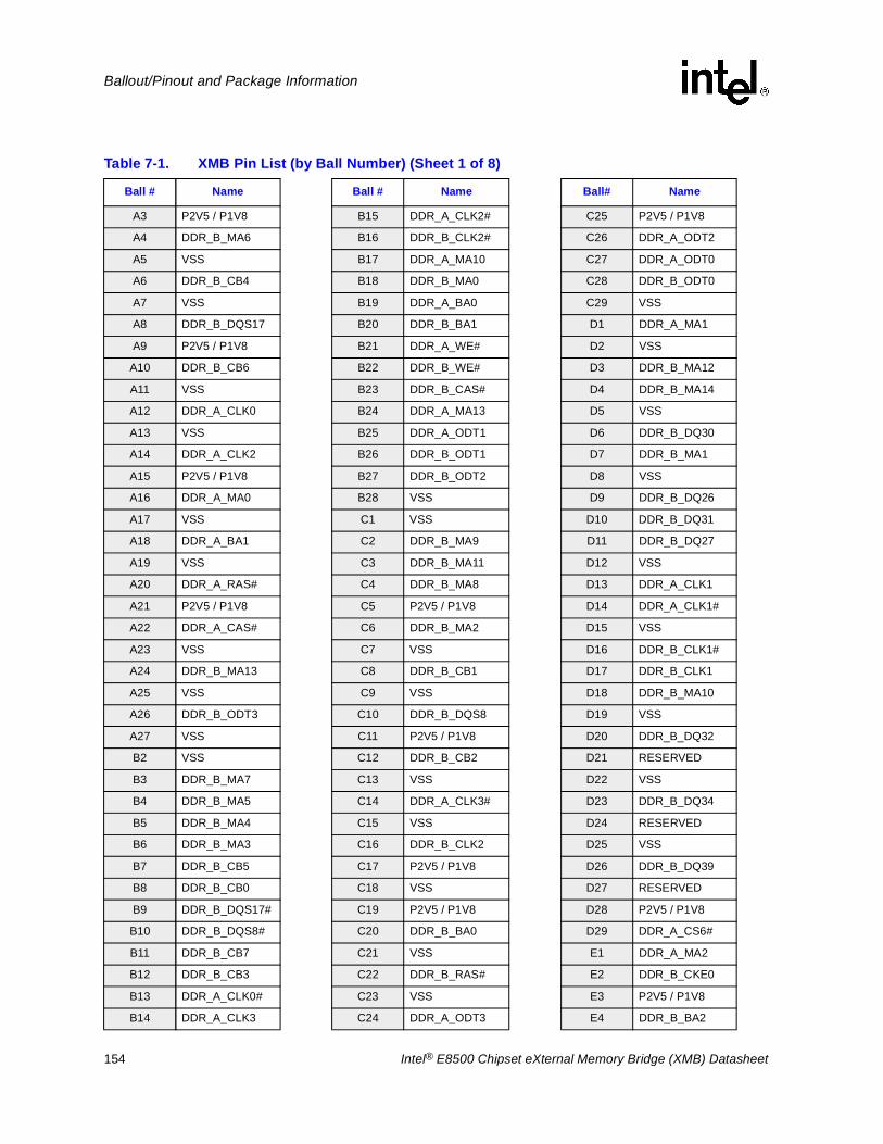
154 Intel® E8500 Chipset eXternal Memory Bridge (XMB) Datasheet
Ballout/Pinout and Package Information
Table 7-1. XMB Pin List (by Ball Number) (Sheet 1 of 8)
Ball # Name Ball # Name Ball# Name
A3 P2V5 / P1V8 B15 DDR_A_CLK2# C25 P2V5 / P1V8
A4 DDR_B_MA6 B16 DDR_B_CLK2# C26 DDR_A_ODT2
A5 VSS B17 DDR_A_MA10 C27 DDR_A_ODT0
A6 DDR_B_CB4 B18 DDR_B_MA0 C28 DDR_B_ODT0
A7 VSS B19 DDR_A_BA0 C29 VSS
A8 DDR_B_DQS17 B20 DDR_B_BA1 D1 DDR_A_MA1
A9 P2V5 / P1V8 B21 DDR_A_WE# D2 VSS
A10 DDR_B_CB6 B22 DDR_B_WE# D3 DDR_B_MA12
A11 VSS B23 DDR_B_CAS# D4 DDR_B_MA14
A12 DDR_A_CLK0 B24 DDR_A_MA13 D5 VSS
A13 VSS B25 DDR_A_ODT1 D6 DDR_B_DQ30
A14 DDR_A_CLK2 B26 DDR_B_ODT1 D7 DDR_B_MA1
A15 P2V5 / P1V8 B27 DDR_B_ODT2 D8 VSS
A16 DDR_A_MA0 B28 VSS D9 DDR_B_DQ26
A17 VSS C1 VSS D10 DDR_B_DQ31
A18 DDR_A_BA1 C2 DDR_B_MA9 D11 DDR_B_DQ27
A19 VSS C3 DDR_B_MA11 D12 VSS
A20 DDR_A_RAS# C4 DDR_B_MA8 D13 DDR_A_CLK1
A21 P2V5 / P1V8 C5 P2V5 / P1V8 D14 DDR_A_CLK1#
A22 DDR_A_CAS# C6 DDR_B_MA2 D15 VSS
A23 VSS C7 VSS D16 DDR_B_CLK1#
A24 DDR_B_MA13 C8 DDR_B_CB1 D17 DDR_B_CLK1
A25 VSS C9 VSS D18 DDR_B_MA10
A26 DDR_B_ODT3 C10 DDR_B_DQS8 D19 VSS
A27 VSS C11 P2V5 / P1V8 D20 DDR_B_DQ32
B2 VSS C12 DDR_B_CB2 D21 RESERVED
B3 DDR_B_MA7 C13 VSS D22 VSS
B4 DDR_B_MA5 C14 DDR_A_CLK3# D23 DDR_B_DQ34
B5 DDR_B_MA4 C15 VSS D24 RESERVED
B6 DDR_B_MA3 C16 DDR_B_CLK2 D25 VSS
B7 DDR_B_CB5 C17 P2V5 / P1V8 D26 DDR_B_DQ39
B8 DDR_B_CB0 C18 VSS D27 RESERVED
B9 DDR_B_DQS17# C19 P2V5 / P1V8 D28 P2V5 / P1V8
B10 DDR_B_DQS8# C20 DDR_B_BA0 D29 DDR_A_CS6#
B11 DDR_B_CB7 C21 VSS E1 DDR_A_MA2
B12 DDR_B_CB3 C22 DDR_B_RAS# E2 DDR_B_CKE0
B13 DDR_A_CLK0# C23 VSS E3 P2V5 / P1V8
B14 DDR_A_CLK3 C24 DDR_A_ODT3 E4 DDR_B_BA2

Intel® E8500 Chipset eXternal Memory Bridge (XMB) Datasheet 155
Ballout/Pinout and Package Information
E5 DDR_B_DQ25 F14 VSS G23 DDR_A_DQS4#
E6 P2V5 / P1V8 F15 RESERVED G24 DDR_A_DQ39
E7 DDR_B_DQS3# F16 P2V5 / P1V8 G25 P2V5 / P1V8
E8 DDR_B_DQS3 F17 DDR_B_CLK0# G26 DDR_B_DQ41
E9 P2V5 / P1V8 F18 DDR_B_CLK0 G27 DDR_B_DQS14
E10 DDR_A_DQ30 F19 VSS G28 VSS
E11 VSS F20 P2V5 / P1V8 G29 DDR_B_CS6#
E12 DDR_A_CB4 F21 DDR_B_DQS13 H1 DDR_A_MA4
E13 P2V5 / P1V8 F22 DDR_B_DQS13# H2 DDR_B_DQ22
E14 DDR_B_CLK3# F23 VSS H3 VSS
E15 DDR_B_CLK3 F24 DDR_A_DQ38 H4 DDR_A_DQ18
E16 GPO8/DDR2# F25 DDR_A_DQ34 H5 DDR_A_DQ23
E17 VSS F26 VSS H6 P2V5 / P1V8
E18 GPO9 F27 DDR_B_DQ45 H7 DDR_A_DQ19
E19 DDR_B_DQ36 F28 DDR_B_DQ40 H8 DDR_A_DQS12#
E20 DDR_B_DQ37 F29 P2V5 / P1V8 H9 P2V5 / P1V8
E21 VSS G1 DDR_A_MA3 H10 DDR_A_DQ31
E22 DDR_B_DQS4# G2 VSS H11 DDR_A_DQ27
E23 DDR_B_DQS4 G3 DDR_B_DQ23 H12 VSS
E24 P2V5 / P1V8 G4 DDR_B_DQ18 H13 P2V5 / P1V8
E25 DDR_B_DQ38 G5 VSS H14 DDR_A_DQS8
E26 DDR_B_DQ35 G6 DDR_B_DQ24 H15 DDR_A_CB0
E27 VSS G7 DDR_A_DQ24 H16 DDR_A_CB2
E28 DDR_B_DQ44 G8 VSS H17 VSS
E29 DDR_A_CS7# G9 DDR_B_DQ29 H18 GPO5
F1 P2V5 / P1V8 G10 DDR_B_DQ28 H19 VSS
F2 DDR_B_CKE1 G11 VSS H20 DDR_A_DQ32
F3 DDR_B_DQ19 G12 DDR_A_CB6 H21 P2V5 / P1V8
F4 VSS G13 DDR_A_DQS17# H22 DDR_A_DQS13
F5 DDR_A_DQ29 G14 DDR_A_DQS8# H23 DDR_A_DQS4
F6 DDR_A_DQ25 G15 VSS H24 VSS
F7 VSS G16 DDR_A_CB3 H25 DDR_A_DQ35
F8 DDR_B_DQS12 G17 GPO7/DDR333# H26 DDR_A_DQ44
F9 DDR_B_DQS12# G18 VSS H27 VSS
F10 VSS G19 GPO6 H28 DDR_B_DQS14#
F11 DDR_A_DQ26 G20 DDR_A_DQ36 H29 DDR_B_CS7#
F12 P2V5 / P1V8 G21 DDR_B_DQ33 J1 VSS
F13 DDR_A_DQS17 G22 VSS J2 DDR_B_DQS2
Table 7-1. XMB Pin List (by Ball Number) (Sheet 2 of 8)
Ball # Name Ball # Name Ball# Name

156 Intel® E8500 Chipset eXternal Memory Bridge (XMB) Datasheet
Ballout/Pinout and Package Information
J3 DDR_B_DQS2# K12 RESERVED L21 RESERVED
J4 P2V5 / P1V8 K13 VSS L22 VSS
J5 DDR_A_DQ22 K14 VSS L23 DDR_A_DQS14#
J6 DDR_A_DQS2 K15 VSS L24 VSS
J7 VSS K16 TESTLO L25 DDR_A_DQS5#
J8 DDR_A_DQS12 K17 GPO1 L26 DDR_B_DQ47
J9 DDR_A_DQS3 K18 VSS L27 P2V5 / P1V8
J10 VSS K19 GPO0 L28 DDR_B_DQ43
J11 DDR_A_DQ28 K20 VSS L29 DDR_A_CS5#
J12 DDR_A_CB5 K21 DDR_A_DQ33 M1 VSS
J13 DDR_A_CB1 K22 P2V5 / P1V8 M2 DDR_B_DQ16
J14 VSS K23 DDR_A_DQS14 M3 DDR_B_DQ20
J15 DDR_A_CB7 K24 DDR_A_DQ41 M4 VSS
J16 P2V5 / P1V8 K25 VSS M5 DDR_A_DQ21
J17 GPO4 K26 DDR_B_DQ46 M6 DDR_A_DQ16
J18 GPO3 K27 DDR_B_DQ42 M7 P2V5 / P1V8
J19 GPO2 K28 VSS M8 XDP_DSTBN
J20 VSS K29 DDR_A_CS4# M9 XDP_D8#
J21 DDR_A_DQ37 L1 DDR_A_MA6 M10 P1V5
J22 DDR_A_DQS13# L2 DDR_B_DQ17 M11 VSS
J23 VSS L3 VSS M12 P1V5
J24 DDR_A_DQ45 L4 DDR_B_DQ21 M13 VSS
J25 DDR_A_DQ40 L5 DDR_A_DQS11 M14 P1V5
J26 P2V5 / P1V8 L6 VSS M15 VSS
J27 DDR_B_DQS5# L7 DDR_A_DQ17 M16 P1V5
J28 DDR_B_DQS5 L8 XDP_DSTBP M17 VSS
J29 VSS L9 P2V5 / P1V8 M18 P1V5
K1 DDR_A_MA5 L10 VSS M19 VSS
K2 P2V5 / P1V8 L11 P1V5 M20 P1V5
K3 DDR_B_DQS11# L12 VSS M21 RESERVED
K4 DDR_B_DQS11 L13 P1V5 M22 RESERVED
K5 VSS L14 VSS M23 P2V5 / P1V8
K6 DDR_A_DQS11# L15 P1V5 M24 DDR_A_DQ46
K7 DDR_A_DQS2# L16 VSS M25 DDR_A_DQS5
K8 VSS L17 P1V5 M26 VSS
K9 DDR_A_DQS3# L18 VSS M27 DDR_B_DQ52
K10 VSS L19 P1V5 M28 DDR_B_DQ53
K11 P2V5 / P1V8 L20 VSS M29 VSS
Table 7-1. XMB Pin List (by Ball Number) (Sheet 3 of 8)
Ball # Name Ball # Name Ball# Name

Intel® E8500 Chipset eXternal Memory Bridge (XMB) Datasheet 157
Ballout/Pinout and Package Information
N1 DDR_A_MA8 P10 P1V5 R19 P1V5
N2 P2V5 / P1V8 P11 VSS R20 VSS
N3 DDR_B_DQ11 P12 P1V5 R21 RESERVED
N4 DDR_B_DQ10 P13 VSS R22 RESERVED
N5 P2V5 / P1V8 P14 P1V5 R23 VSS
N6 DDR_A_DQ20 P15 VSS R24 DDR_A_DQ48
N7 DDR_A_DQ11 P16 VCCA R25 DDR_A_DQ53
N8 VSS P17 VSSA R26 VSS
N9 XDP_D0# P18 P1V5 R27 DDR_B_DQS6
N10 VSS P19 VSS R28 DDR_B_DQS6#
N11 P1V5 P20 P1V5 R29 P2V5 / P1V8
N12 VSS P21 RESERVED T1 DDR_A_MA11
N13 P1V5 P22 RESERVED T2 VSS
N14 VSS P23 DDR_A_DQ52 T3 DDR_B_DQS10#
N15 P1V5 P24 P2V5 / P1V8 T4 DDR_B_DQS10
N16 VSS P25 DDR_A_DQ43 T5 P2V5 / P1V8
N17 P1V5 P26 DDR_B_DQS15 T6 DDR_A_DQS10#
N18 VSS P27 DDR_B_DQS15# T7 DDR_A_DQS1#
N19 P1V5 P28 VSS T8 XDP_D11#
N20 VSS P29 DDR_B_CS5# T9 XDP_D3#
N21 RESERVED R1 P2V5 / P1V8 T10 P1V5
N22 VSS R2 DDR_B_DQS1 T11 VSS
N23 DDR_A_DQ47 R3 DDR_B_DQS1# T12 P1V5
N24 DDR_A_DQ42 R4 VSS T13 VSS
N25 VSS R5 DDR_A_DQ14 T14 P1V5
N26 DDR_B_DQ48 R6 DDR_A_DQS1 T15 VSS
N27 DDR_B_DQ49 R7 VSS T16 VCCA_IMI
N28 P2V5 / P1V8 R8 XDP_D10# T17 VSS
N29 DDR_B_CS4# R9 XDP_D2# T18 P1V5
P1 DDR_A_MA7 R10 VSS T19 VSS
P2 DDR_B_DQ15 R11 P1V5 T20 P1V5
P3 VSS R12 VSS T21 RESERVED
P4 DDR_B_DQ14 R13 P1V5 T22 RESERVED
P5 DDR_A_DQ10 R14 VSS T23 DDR_A_DQS15
P6 VSS R15 P1V5 T24 DDR_A_DQ49
P7 DDR_A_DQ15 R16 VSS T25 P2V5 / P1V8
P8 XDP_D9# R17 P1V5 T26 DDR_B_DQ55
P9 XDP_D1# R18 VSS T27 DDR_B_DQ54
Table 7-1. XMB Pin List (by Ball Number) (Sheet 4 of 8)
Ball # Name Ball # Name Ball# Name

158 Intel® E8500 Chipset eXternal Memory Bridge (XMB) Datasheet
Ballout/Pinout and Package Information
T28 VSS V8 XDP_D13# W17 P1V5
T29 DDR_A_CS2# V9 XDP_D5# W18 VSS
U1 DDR_A_MA9 V10 P1V5 W19 P1V5
U2 DDR_B_DQ9 V11 VSS W20 VSS
U3 VSS V12 P1V5 W21 RESERVED
U4 DDR_B_DQ13 V13 VSS W22 RESERVED
U5 DDR_A_DQS10 V14 P1V5 W23 DDR_A_DQ50
U6 VSS V15 VSS W24 DDR_A_DQ55
U7 DDR_A_DQ9 V16 IMI_VCCBG W25 VSS
U8 XDP_D12# V17 IMI_VSSBG W26 DDR_B_DQ57
U9 XDP_D4# V18 P1V5 W27 DDR_B_DQ56
U10 VSS V19 VSS W28 VSS
U11 P1V5 V20 P1V5 W29 DDR_B_CS2#
U12 VSS V21 RESERVED Y1 DDR_A_BA2
U13 P1V5 V22 RESERVED Y2 DDR_B_DQ2
U14 VSS V23 VSS Y3 VSS
U15 P1V5 V24 DDR_A_DQ54 Y4 DDR_B_DQ6
U16 VSSA_IMI V25 DDR_A_DQS6 Y5 DDR_A_DQ7
U17 P1V5 V26 P2V5 / P1V8 Y6 P2V5 / P1V8
U18 VSS V27 DDR_B_DQ61 Y7 DDR_A_DQ2
U19 P1V5 V28 DDR_B_DQ60 Y8 XDP_D15#
U20 VSS V29 VSS Y9 XDP_D7#
U21 RESERVED W1 DDR_A_MA12 Y10 P1V5
U22 RESERVED W2 P2V5 / P1V8 Y11 VSS
U23 DDR_A_DQS15# W3 DDR_B_DQ3 Y12 P1V5
U24 VSS W4 DDR_B_DQ7 Y13 VSS
U25 DDR_A_DQS6# W5 VSS Y14 P1V5
U26 DDR_B_DQ51 W6 DDR_A_DQ8 Y15 VSS
U27 VSS W7 DDR_A_DQ3 Y16 P1V5
U28 DDR_B_DQ50 W8 XDP_D14# Y17 VSS
U29 DDR_A_CS3# W9 XDP_D6# Y18 P1V5
V1 VSS W10 VSS Y19 VSS
V2 DDR_B_DQ12 W11 P1V5 Y20 P1V5
V3 DDR_B_DQ8 W12 VSS Y21 RESERVED
V4 P2V5 / P1V8 W13 P1V5 Y22 RESERVED
V5 DDR_A_DQ13 W14 VSS Y23 DDR_A_DQ60
V6 DDR_A_DQ12 W15 P1V5 Y24 VSS
V7 VSS W16 VSS Y25 DDR_A_DQ51
Table 7-1. XMB Pin List (by Ball Number) (Sheet 5 of 8)
Ball # Name Ball # Name Ball# Name

Intel® E8500 Chipset eXternal Memory Bridge (XMB) Datasheet 159
Ballout/Pinout and Package Information
Y26 P2V5 / P1V8 AB6 DDR_A_DQS0# AC15 IMI_RXP6
Y27 DDR_B_DQS16# AB7 RESERVED AC16 IMI_RXN6
Y28 DDR_B_DQS16 AB8 TESTLO AC17 VSS
Y29 DDR_B_CS3# AB9 TESTHI AC18 IMI_RXP3
AA1 P2V5 / P1V8 AB10 VSS AC19 IMI_RXN3
AA2 DDR_B_DQS0 AB11 P1V5 AC20 VSS
AA3 DDR_B_DQS0# AB12 VSS AC21 TRST#
AA4 VSS AB13 VSS AC22 TDO
AA5 DDR_A_DQ6 AB14 VSS AC23 VSS
AA6 DDR_A_DQS0 AB15 VSS AC24 P2V5 / P1V8
AA7 VSS AB16 VSS AC25 DDR_A_DQS16#
AA8 RST# AB17 SMBDATA AC26 DDR_A_DQS7#
AA9 PWRGOOD AB18 SMBCLK AC27 VSS
AA10 TESTLO AB19 VSS AC28 DDR_B_DQ58
AA11 IMI_FRAME AB20 RESERVED AC29 DDR_A_CS1#
AA12 VSS AB21 VSS AD1 VSS
AA13 TESTHI AB22 P2V5 / P1V8 AD2 DDR_B_DQ0
AA14 TESTLO AB23 DDR_A_DQ57 AD3 DDR_B_DQ4
AA15 VSS AB24 DDR_A_DQS16 AD4 P2V5 / P1V8
AA16 IMI_CLKP AB25 VSS AD5 DDR_A_DQS9
AA17 IMI_CLKN AB26 DDR_B_DQ63 AD6 VSS
AA18 VSS AB27 DDR_B_DQ62 AD7 IMI_LINKP1
AA19 SMBA1 AB28 VSS AD8 IMI_LINKN1
AA20 SMBA0 AB29 DDR_A_CS0# AD9 VSS
AA21 RESERVED AC1 DDR_A_CKE0 AD10 IMI_TXP13
AA22 RESERVED AC2 DDR_B_DQ1 AD11 IMI_TXN13
AA23 P2V5 / P1V8 AC3 VSS AD12 P1V5
AA24 DDR_A_DQ61 AC4 DDR_B_DQ5 AD13 IMI_RXP8
AA25 DDR_A_DQ56 AC5 DDR_A_DQS9# AD14 IMI_RXN8
AA26 VSS AC6 VSS AD15 VSS
AA27 DDR_B_DQS7 AC7 VSS AD16 IMI_RXP5
AA28 DDR_B_DQS7# AC8 P1V5 AD17 IMI_RXN5
AA29 P2V5 / P1V8 AC9 IMI_TXP15 AD18 P1V5
AB1 DDR_A_MA14 AC10 IMI_TXN15 AD19 IMI_RXP2
AB2 VSS AC11 VSS AD20 IMI_RXN2
AB3 DDR_B_DQS9# AC12 IMI_RXP9 AD21 VSS
AB4 DDR_B_DQS9 AC13 IMI_RXN9 AD22 TDI
AB5 P2V5 / P1V8 AC14 P1V5 AD23 TMS
Table 7-1. XMB Pin List (by Ball Number) (Sheet 6 of 8)
Ball # Name Ball # Name Ball# Name

160 Intel® E8500 Chipset eXternal Memory Bridge (XMB) Datasheet
Ballout/Pinout and Package Information
AD24 VSS AF4 VSS AG13 IMI_TXP8
AD25 DDR_A_DQ62 AF5 VSS AG14 IMI_TXN8
AD26 P2V5 / P1V8 AF6 IMI_LINKP2 AG15 VSS
AD27 DDR_A_DQS7 AF7 IMI_LINKN2 AG16 IMI_TXP5
AD28 DDR_B_DQ59 AF8 P1V5 AG17 IMI_TXN5
AD29 VSS AF9 IMI_TXP14 AG18 P1V5
AE1 DDR_A_CKE1 AF10 IMI_TXN14 AG19 IMI_TXP2
AE2 VSS AF11 VSS AG20 IMI_TXN2
AE3 DDR_A_DQ5 AF12 IMI_TXP9 AG21 VSS
AE4 DDR_A_DQ1 AF13 IMI_TXN9 AG22 IMI_TXP0
AE5 VSS AF14 P1V5 AG23 IMI_TXN0
AE6 P1V5 AF15 IMI_TXP6 AG24 VSS
AE7 VSS AF16 IMI_TXN6 AG25 DDR_TRES1
AE8 IMI_TXP17 AF17 VSS AG26 DDR_TRES0
AE9 IMI_TXN17 AF18 IMI_TXP3 AG27 SPD_SMBCLK
AE10 P1V5 AF19 IMI_TXN3 AG28 SPD_SMBDATA
AE11 IMI_TXP11 AF20 P1V5 AG29 VSS
AE12 IMI_TXN11 AF21 IMI_RXP0 AH2 VSS
AE13 VSS AF22 IMI_RXN0 AH3 RESERVED
AE14 IMI_RXP7 AF23 VSS AH4 RESERVED
AE15 IMI_RXN7 AF24 VSS AH5 VSS
AE16 P1V5 AF25 DDR_CRES AH6 P1V5
AE17 IMI_RXP4 AF26 VSS AH7 VSS
AE18 IMI_RXN4 AF27 P2V5 / P1V8 AH8 IMI_TXP16
AE19 VSS AF28 DDR_A_DQ59 AH9 IMI_TXN16
AE20 IMI_RXP1 AF29 DDR_B_CS1# AH10 P1V5
AE21 IMI_RXN1 AG1 P2V5 / P1V8 AH11 IMI_TXP10
AE22 VSS AG2 DDR_A_VREF AH12 IMI_TXN10
AE23 TCK AG3 VSS AH13 VSS
AE24 RESERVED AG4 RESERVED AH14 IMI_TXP7
AE25 P2V5 / P1V8 AG5 RESERVED AH15 IMI_TXN7
AE26 DDR_A_DQ63 AG6 VSS AH16 P1V5
AE27 DDR_A_DQ58 AG7 IMI_LINKP0 AH17 IMI_TXP4
AE28 VSS AG8 IMI_LINKN0 AH18 IMI_TXN4
AE29 DDR_B_CS0# AG9 VSS AH19 VSS
AF1 DDR_B_VREF AG10 IMI_TXP12 AH20 IMI_TXP1
AF2 DDR_A_DQ4 AG11 IMI_TXN12 AH21 IMI_TXN1
AF3 DDR_A_DQ0 AG12 P1V5 AH22 P1V5
Table 7-1. XMB Pin List (by Ball Number) (Sheet 7 of 8)
Ball # Name Ball # Name Ball# Name

Intel® E8500 Chipset eXternal Memory Bridge (XMB) Datasheet 161
Ballout/Pinout and Package Information
AH23 IMI_ICOMPI AJ8 VSS AJ19 P1V5
AH24 IMI_ICOMPO AJ9 P1V5 AJ20 VSS
AH25 VSS AJ10 VSS AJ21 P1V5
AH26 DDR_SLWCRES AJ11 P1V5 AJ22 VSS
AH27 DDR_DRVCRES AJ12 VSS AJ23 P1V5
AH28 VSS AJ13 P1V5 AJ24 VSS
AJ3 VSS AJ14 VSS AJ25 P1V5
AJ4 XDP_CRES AJ15 P1V5 AJ26 V3REF
AJ5 XDP_ODTCRES AJ16 VSS AJ27 VSS
AJ6 XDP_SLWCRES AJ17 P1V5
AJ7 P1V5 AJ18 VSS
Table 7-1. XMB Pin List (by Ball Number) (Sheet 8 of 8)
Ball # Name Ball # Name Ball# Name

162 Intel® E8500 Chipset eXternal Memory Bridge (XMB) Datasheet
Ballout/Pinout and Package Information
Table 7-2. XMB Pin List (By Pin Name) (Sheet 1 of 8)
Ball # Name Ball # Name Ball# Name
B19 DDR_A_BA0 W6 DDR_A_DQ8 M24 DDR_A_DQ46
A18 DDR_A_BA1 U7 DDR_A_DQ9 N23 DDR_A_DQ47
Y1 DDR_A_BA2 P5 DDR_A_DQ10 R24 DDR_A_DQ48
A22 DDR_A_CAS# N7 DDR_A_DQ11 T24 DDR_A_DQ49
H15 DDR_A_CB0 V6 DDR_A_DQ12 W23 DDR_A_DQ50
J13 DDR_A_CB1 V5 DDR_A_DQ13 Y25 DDR_A_DQ51
H16 DDR_A_CB2 R5 DDR_A_DQ14 P23 DDR_A_DQ52
G16 DDR_A_CB3 P7 DDR_A_DQ15 R25 DDR_A_DQ53
E12 DDR_A_CB4 M6 DDR_A_DQ16 V24 DDR_A_DQ54
J12 DDR_A_CB5 L7 DDR_A_DQ17 W24 DDR_A_DQ55
G12 DDR_A_CB6 H4 DDR_A_DQ18 AA25 DDR_A_DQ56
J15 DDR_A_CB7 H7 DDR_A_DQ19 AB23 DDR_A_DQ57
AC1 DDR_A_CKE0 N6 DDR_A_DQ20 AE27 DDR_A_DQ58
AE1 DDR_A_CKE1 M5 DDR_A_DQ21 AF28 DDR_A_DQ59
A12 DDR_A_CLK0 J5 DDR_A_DQ22 Y23 DDR_A_DQ60
B13 DDR_A_CLK0# H5 DDR_A_DQ23 AA24 DDR_A_DQ61
D13 DDR_A_CLK1 G7 DDR_A_DQ24 AD25 DDR_A_DQ62
D14 DDR_A_CLK1# F6 DDR_A_DQ25 AE26 DDR_A_DQ63
A14 DDR_A_CLK2 F11 DDR_A_DQ26 AA6 DDR_A_DQS0
B15 DDR_A_CLK2# H11 DDR_A_DQ27 AB6 DDR_A_DQS0#
B14 DDR_A_CLK3 J11 DDR_A_DQ28 R6 DDR_A_DQS1
C14 DDR_A_CLK3# F5 DDR_A_DQ29 T7 DDR_A_DQS1#
AB29 DDR_A_CS0# E10 DDR_A_DQ30 J6 DDR_A_DQS2
AC29 DDR_A_CS1# H10 DDR_A_DQ31 K7 DDR_A_DQS2#
T29 DDR_A_CS2# H20 DDR_A_DQ32 J9 DDR_A_DQS3
U29 DDR_A_CS3# K21 DDR_A_DQ33 K9 DDR_A_DQS3#
K29 DDR_A_CS4# F25 DDR_A_DQ34 H23 DDR_A_DQS4
L29 DDR_A_CS5# H25 DDR_A_DQ35 G23 DDR_A_DQS4#
D29 DDR_A_CS6# G20 DDR_A_DQ36 M25 DDR_A_DQS5
E29 DDR_A_CS7# J21 DDR_A_DQ37 L25 DDR_A_DQS5#
AF3 DDR_A_DQ0 F24 DDR_A_DQ38 V25 DDR_A_DQS6
AE4 DDR_A_DQ1 G24 DDR_A_DQ39 U25 DDR_A_DQS6#
Y7 DDR_A_DQ2 J25 DDR_A_DQ40 AD27 DDR_A_DQS7
W7 DDR_A_DQ3 K24 DDR_A_DQ41 AC26 DDR_A_DQS7#
AF2 DDR_A_DQ4 N24 DDR_A_DQ42 H14 DDR_A_DQS8
AE3 DDR_A_DQ5 P25 DDR_A_DQ43 G14 DDR_A_DQS8#
AA5 DDR_A_DQ6 H26 DDR_A_DQ44 AD5 DDR_A_DQS9
Y5 DDR_A_DQ7 J24 DDR_A_DQ45 AC5 DDR_A_DQS9#

Intel® E8500 Chipset eXternal Memory Bridge (XMB) Datasheet 163
Ballout/Pinout and Package Information
U5 DDR_A_DQS10 C20 DDR_B_BA0 V3 DDR_B_DQ8
T6 DDR_A_DQS10# B20 DDR_B_BA1 U2 DDR_B_DQ9
L5 DDR_A_DQS11 E4 DDR_B_BA2 N4 DDR_B_DQ10
K6 DDR_A_DQS11# B23 DDR_B_CAS# N3 DDR_B_DQ11
J8 DDR_A_DQS12 B8 DDR_B_CB0 V2 DDR_B_DQ12
H8 DDR_A_DQS12# C8 DDR_B_CB1 U4 DDR_B_DQ13
H22 DDR_A_DQS13 C12 DDR_B_CB2 P4 DDR_B_DQ14
J22 DDR_A_DQS13# B12 DDR_B_CB3 P2 DDR_B_DQ15
K23 DDR_A_DQS14 A6 DDR_B_CB4 M2 DDR_B_DQ16
L23 DDR_A_DQS14# B7 DDR_B_CB5 L2 DDR_B_DQ17
T23 DDR_A_DQS15 A10 DDR_B_CB6 G4 DDR_B_DQ18
U23 DDR_A_DQS15# B11 DDR_B_CB7 F3 DDR_B_DQ19
AB24 DDR_A_DQS16 E2 DDR_B_CKE0 M3 DDR_B_DQ20
AC25 DDR_A_DQS16# F2 DDR_B_CKE1 L4 DDR_B_DQ21
F13 DDR_A_DQS17 F18 DDR_B_CLK0 H2 DDR_B_DQ22
G13 DDR_A_DQS17# F17 DDR_B_CLK0# G3 DDR_B_DQ23
A16 DDR_A_MA0 D17 DDR_B_CLK1 G6 DDR_B_DQ24
D1 DDR_A_MA1 D16 DDR_B_CLK1# E5 DDR_B_DQ25
E1 DDR_A_MA2 C16 DDR_B_CLK2 D9 DDR_B_DQ26
G1 DDR_A_MA3 B16 DDR_B_CLK2# D11 DDR_B_DQ27
H1 DDR_A_MA4 E15 DDR_B_CLK3 G10 DDR_B_DQ28
K1 DDR_A_MA5 E14 DDR_B_CLK3# G9 DDR_B_DQ29
L1 DDR_A_MA6 AE29 DDR_B_CS0# D6 DDR_B_DQ30
P1 DDR_A_MA7 AF29 DDR_B_CS1# D10 DDR_B_DQ31
N1 DDR_A_MA8 W29 DDR_B_CS2# D20 DDR_B_DQ32
U1 DDR_A_MA9 Y29 DDR_B_CS3# G21 DDR_B_DQ33
B17 DDR_A_MA10 N29 DDR_B_CS4# D23 DDR_B_DQ34
T1 DDR_A_MA11 P29 DDR_B_CS5# E26 DDR_B_DQ35
W1 DDR_A_MA12 G29 DDR_B_CS6# E19 DDR_B_DQ36
B24 DDR_A_MA13 H29 DDR_B_CS7# E20 DDR_B_DQ37
AB1 DDR_A_MA14 AD2 DDR_B_DQ0 E25 DDR_B_DQ38
C27 DDR_A_ODT0 AC2 DDR_B_DQ1 D26 DDR_B_DQ39
B25 DDR_A_ODT1 Y2 DDR_B_DQ2 F28 DDR_B_DQ40
C26 DDR_A_ODT2 W3 DDR_B_DQ3 G26 DDR_B_DQ41
C24 DDR_A_ODT3 AD3 DDR_B_DQ4 K27 DDR_B_DQ42
A20 DDR_A_RAS# AC4 DDR_B_DQ5 L28 DDR_B_DQ43
AG2 DDR_A_VREF Y4 DDR_B_DQ6 E28 DDR_B_DQ44
B21 DDR_A_WE# W4 DDR_B_DQ7 F27 DDR_B_DQ45
Table 7-2. XMB Pin List (By Pin Name) (Sheet 2 of 8)
Ball # Name Ball # Name Ball# Name

164 Intel® E8500 Chipset eXternal Memory Bridge (XMB) Datasheet
Ballout/Pinout and Package Information
K26 DDR_B_DQ46 T4 DDR_B_DQS10 AF25 DDR_CRES
L26 DDR_B_DQ47 T3 DDR_B_DQS10# AH27 DDR_DRVCRES
N26 DDR_B_DQ48 K4 DDR_B_DQS11 AH26 DDR_SLWCRES
N27 DDR_B_DQ49 K3 DDR_B_DQS11# AG26 DDR_TRES0
U28 DDR_B_DQ50 F8 DDR_B_DQS12 AG25 DDR_TRES1
U26 DDR_B_DQ51 F9 DDR_B_DQS12# K19 GPO0
M27 DDR_B_DQ52 F21 DDR_B_DQS13 K17 GPO1
M28 DDR_B_DQ53 F22 DDR_B_DQS13# J19 GPO2
T27 DDR_B_DQ54 G27 DDR_B_DQS14 J18 GPO3
T26 DDR_B_DQ55 H28 DDR_B_DQS14# J17 GPO4
W27 DDR_B_DQ56 P26 DDR_B_DQS15 H18 GPO5
W26 DDR_B_DQ57 P27 DDR_B_DQS15# G19 GPO6
AC28 DDR_B_DQ58 Y28 DDR_B_DQS16 G17 GPO7/DDR333#
AD28 DDR_B_DQ59 Y27 DDR_B_DQS16# E16 GPO8/DDR2#
V28 DDR_B_DQ60 A8 DDR_B_DQS17 E18 GPO9
V27 DDR_B_DQ61 B9 DDR_B_DQS17# AA17 IMI_CLKN
AB27 DDR_B_DQ62 B18 DDR_B_MA0 AA16 IMI_CLKP
AB26 DDR_B_DQ63 D7 DDR_B_MA1 AA11 IMI_FRAME
AA2 DDR_B_DQS0 C6 DDR_B_MA2 AH23 IMI_ICOMPI
AA3 DDR_B_DQS0# B6 DDR_B_MA3 AH24 IMI_ICOMPO
R2 DDR_B_DQS1 B5 DDR_B_MA4 AG8 IMI_LINKN0
R3 DDR_B_DQS1# B4 DDR_B_MA5 AG7 IMI_LINKP0
J2 DDR_B_DQS2 A4 DDR_B_MA6 AD8 IMI_LINKN1
J3 DDR_B_DQS2# B3 DDR_B_MA7 AD7 IMI_LINKP1
E8 DDR_B_DQS3 C4 DDR_B_MA8 AF7 IMI_LINKN2
E7 DDR_B_DQS3# C2 DDR_B_MA9 AF6 IMI_LINKP2
E23 DDR_B_DQS4 D18 DDR_B_MA10 AF22 IMI_RXN0
E22 DDR_B_DQS4# C3 DDR_B_MA11 AF21 IMI_RXP0
J28 DDR_B_DQS5 D3 DDR_B_MA12 AE21 IMI_RXN1
J27 DDR_B_DQS5# A24 DDR_B_MA13 AE20 IMI_RXP1
R27 DDR_B_DQS6 D4 DDR_B_MA14 AD20 IMI_RXN2
R28 DDR_B_DQS6# C28 DDR_B_ODT0 AD19 IMI_RXP2
AA27 DDR_B_DQS7 B26 DDR_B_ODT1 AC19 IMI_RXN3
AA28 DDR_B_DQS7# B27 DDR_B_ODT2 AC18 IMI_RXP3
C10 DDR_B_DQS8 A26 DDR_B_ODT3 AE18 IMI_RXN4
B10 DDR_B_DQS8# C22 DDR_B_RAS# AE17 IMI_RXP4
AB4 DDR_B_DQS9 AF1 DDR_B_VREF AD17 IMI_RXN5
AB3 DDR_B_DQS9# B22 DDR_B_WE# AD16 IMI_RXP5
Table 7-2. XMB Pin List (By Pin Name) (Sheet 3 of 8)
Ball # Name Ball # Name Ball# Name
Intel® E8500 Chipset eXternal Memory Bridge (XMB) Datasheet 165
Ballout/Pinout and Package Information
AC16 IMI_RXN6 AC10 IMI_TXN15 L13 P1V5
AC15 IMI_RXP6 AC9 IMI_TXP15 L15 P1V5
AE15 IMI_RXN7 AH9 IMI_TXN16 L17 P1V5
AE14 IMI_RXP7 AH8 IMI_TXP16 L19 P1V5
AD14 IMI_RXN8 AE9 IMI_TXN17 M10 P1V5
AD13 IMI_RXP8 AE8 IMI_TXP17 M12 P1V5
AC13 IMI_RXN9 T16 IMI_VCCA M14 P1V5
AC12 IMI_RXP9 V16 IMI_VCCBG M16 P1V5
AG23 IMI_TXN0 U16 IMI_VSSA M18 P1V5
AG22 IMI_TXP0 V17 IMI_VSSBG M20 P1V5
AH21 IMI_TXN1 AB11 P1V5 N11 P1V5
AH20 IMI_TXP1 AC8 P1V5 N13 P1V5
AG20 IMI_TXN2 AC14 P1V5 N15 P1V5
AG19 IMI_TXP2 AD12 P1V5 N17 P1V5
AF19 IMI_TXN3 AD18 P1V5 N19 P1V5
AF18 IMI_TXP3 AE6 P1V5 P10 P1V5
AH18 IMI_TXN4 AE10 P1V5 P12 P1V5
AH17 IMI_TXP4 AE16 P1V5 P14 P1V5
AG17 IMI_TXN5 AF14 P1V5 P18 P1V5
AG16 IMI_TXP5 AF8 P1V5 P20 P1V5
AF16 IMI_TXN6 AF20 P1V5 R11 P1V5
AF15 IMI_TXP6 AG12 P1V5 R13 P1V5
AH15 IMI_TXN7 AG18 P1V5 R15 P1V5
AH14 IMI_TXP7 AH6 P1V5 R17 P1V5
AG14 IMI_TXN8 AH10 P1V5 R19 P1V5
AG13 IMI_TXP8 AH16 P1V5 T10 P1V5
AF13 IMI_TXN9 AH22 P1V5 T12 P1V5
AF12 IMI_TXP9 AJ7 P1V5 T14 P1V5
AH12 IMI_TXN10 AJ9 P1V5 T18 P1V5
AH11 IMI_TXP10 AJ11 P1V5 T20 P1V5
AE12 IMI_TXN11 AJ13 P1V5 U11 P1V5
AE11 IMI_TXP11 AJ15 P1V5 U13 P1V5
AG11 IMI_TXN12 AJ17 P1V5 U15 P1V5
AG10 IMI_TXP12 AJ19 P1V5 U17 P1V5
AD11 IMI_TXN13 AJ21 P1V5 U19 P1V5
AD10 IMI_TXP13 AJ23 P1V5 V10 P1V5
AF10 IMI_TXN14 AJ25 P1V5 V12 P1V5
AF9 IMI_TXP14 L11 P1V5 V14 P1V5
Table 7-2. XMB Pin List (By Pin Name) (Sheet 4 of 8)
Ball # Name Ball # Name Ball# Name

166 Intel® E8500 Chipset eXternal Memory Bridge (XMB) Datasheet
Ballout/Pinout and Package Information
V18 P1V5 E24 P2V5 / P1V8 AB20 RESERVED
V20 P1V5 F1 P2V5 / P1V8 AE24 RESERVED
W11 P1V5 F12 P2V5 / P1V8 AG4 RESERVED
W13 P1V5 F16 P2V5 / P1V8 AG5 RESERVED
W15 P1V5 F20 P2V5 / P1V8 AH3 RESERVED
W17 P1V5 F29 P2V5 / P1V8 AH4 RESERVED
W19 P1V5 G25 P2V5 / P1V8 D21 RESERVED
Y10 P1V5 H6 P2V5 / P1V8 D24 RESERVED
Y12 P1V5 H9 P2V5 / P1V8 D27 RESERVED
Y14 P1V5 H13 P2V5 / P1V8 F15 RESERVED
Y16 P1V5 H21 P2V5 / P1V8 K12 RESERVED
Y18 P1V5 J4 P2V5 / P1V8 L21 RESERVED
Y20 P1V5 J16 P2V5 / P1V8 M21 RESERVED
A3 P2V5 / P1V8 J26 P2V5 / P1V8 M22 RESERVED
A9 P2V5 / P1V8 K2 P2V5 / P1V8 N21 RESERVED
A15 P2V5 / P1V8 K11 P2V5 / P1V8 P21 RESERVED
A21 P2V5 / P1V8 K22 P2V5 / P1V8 P22 RESERVED
AA1 P2V5 / P1V8 L9 P2V5 / P1V8 R21 RESERVED
AA23 P2V5 / P1V8 L27 P2V5 / P1V8 R22 RESERVED
AA29 P2V5 / P1V8 M7 P2V5 / P1V8 T21 RESERVED
AB5 P2V5 / P1V8 M23 P2V5 / P1V8 T22 RESERVED
AB22 P2V5 / P1V8 N2 P2V5 / P1V8 U21 RESERVED
AC24 P2V5 / P1V8 N5 P2V5 / P1V8 U22 RESERVED
AD4 P2V5 / P1V8 N28 P2V5 / P1V8 V21 RESERVED
AD26 P2V5 / P1V8 P24 P2V5 / P1V8 V22 RESERVED
AE25 P2V5 / P1V8 R1 P2V5 / P1V8 W21 RESERVED
AF27 P2V5 / P1V8 R29 P2V5 / P1V8 W22 RESERVED
AG1 P2V5 / P1V8 T5 P2V5 / P1V8 Y21 RESERVED
C5 P2V5 / P1V8 T25 P2V5 / P1V8 Y22 RESERVED
C11 P2V5 / P1V8 V4 P2V5 / P1V8 AA8 RST#
C17 P2V5 / P1V8 V26 P2V5 / P1V8 AA20 SMBA0
C19 P2V5 / P1V8 W2 P2V5 / P1V8 AA19 SMBA1
C25 P2V5 / P1V8 Y6 P2V5 / P1V8 AB18 SMBCLK
D28 P2V5 / P1V8 Y26 P2V5 / P1V8 AB17 SMBDATA
E3 P2V5 / P1V8 AA9 PWRGOOD AG27 SPD_SMBCLK
E6 P2V5 / P1V8 AA21 RESERVED AG28 SPD_SMBDATA
E9 P2V5 / P1V8 AA22 RESERVED AE23 TCK
E13 P2V5 / P1V8 AB7 RESERVED AD22 TDI
Table 7-2. XMB Pin List (By Pin Name) (Sheet 5 of 8)
Ball # Name Ball # Name Ball# Name

Intel® E8500 Chipset eXternal Memory Bridge (XMB) Datasheet 167
Ballout/Pinout and Package Information
AC22 TDO AC6 VSS AH13 VSS
AA13 TESTHI AC7 VSS AH19 VSS
AB9 TESTHI AC11 VSS AH25 VSS
AA10 TESTLO AC17 VSS AH28 VSS
AA14 TESTLO AC20 VSS AJ3 VSS
AB8 TESTLO AC23 VSS AJ8 VSS
K16 TESTLO AC27 VSS AJ10 VSS
AD23 TMS AD1 VSS AJ12 VSS
AC21 TRST# AD6 VSS AJ14 VSS
AJ26 V3REF AD9 VSS AJ16 VSS
P16 VCCA AD15 VSS AJ18 VSS
A5 VSS AD21 VSS AJ20 VSS
A7 VSS AD24 VSS AJ22 VSS
A11 VSS AD29 VSS AJ24 VSS
A13 VSS AE2 VSS AJ27 VSS
A17 VSS AE5 VSS B2 VSS
A19 VSS AE7 VSS B28 VSS
A23 VSS AE13 VSS C1 VSS
A25 VSS AE19 VSS C7 VSS
A27 VSS AE22 VSS C9 VSS
AA4 VSS AE28 VSS C13 VSS
AA7 VSS AF4 VSS C15 VSS
AA12 VSS AF5 VSS C18 VSS
AA15 VSS AF11 VSS C21 VSS
AA18 VSS AF17 VSS C23 VSS
AA26 VSS AF23 VSS C29 VSS
AB2 VSS AF24 VSS D2 VSS
AB10 VSS AF26 VSS D5 VSS
AB12 VSS AG3 VSS D8 VSS
AB13 VSS AG6 VSS D12 VSS
AB14 VSS AG9 VSS D15 VSS
AB15 VSS AG15 VSS D19 VSS
AB16 VSS AG21 VSS D22 VSS
AB19 VSS AG24 VSS D25 VSS
AB21 VSS AG29 VSS E11 VSS
AB25 VSS AH2 VSS E17 VSS
AB28 VSS AH5 VSS E21 VSS
AC3 VSS AH7 VSS E27 VSS
Table 7-2. XMB Pin List (By Pin Name) (Sheet 6 of 8)
Ball # Name Ball # Name Ball# Name

168 Intel® E8500 Chipset eXternal Memory Bridge (XMB) Datasheet
Ballout/Pinout and Package Information
F4 VSS L3 VSS R12 VSS
F7 VSS L6 VSS R14 VSS
F10 VSS L10 VSS R16 VSS
F14 VSS L12 VSS R18 VSS
F19 VSS L14 VSS R20 VSS
F23 VSS L16 VSS R23 VSS
F26 VSS L18 VSS R26 VSS
G2 VSS L20 VSS T2 VSS
G5 VSS L22 VSS T11 VSS
G8 VSS L24 VSS T13 VSS
G11 VSS M1 VSS T15 VSS
G15 VSS M4 VSS T17 VSS
G18 VSS M11 VSS T19 VSS
G22 VSS M13 VSS T28 VSS
G28 VSS M15 VSS U3 VSS
H3 VSS M17 VSS U6 VSS
H12 VSS M19 VSS U10 VSS
H17 VSS M26 VSS U12 VSS
H19 VSS M29 VSS U14 VSS
H24 VSS N8 VSS U18 VSS
H27 VSS N10 VSS U20 VSS
J1 VSS N12 VSS U24 VSS
J7 VSS N14 VSS U27 VSS
J10 VSS N16 VSS V1 VSS
J14 VSS N18 VSS V7 VSS
J20 VSS N20 VSS V11 VSS
J23 VSS N22 VSS V13 VSS
J29 VSS N25 VSS V15 VSS
K5 VSS P3 VSS V19 VSS
K8 VSS P6 VSS V23 VSS
K10 VSS P11 VSS V29 VSS
K13 VSS P13 VSS W5 VSS
K14 VSS P15 VSS W10 VSS
K15 VSS P19 VSS W12 VSS
K18 VSS P28 VSS W14 VSS
K20 VSS R4 VSS W16 VSS
K25 VSS R7 VSS W18 VSS
K28 VSS R10 VSS W20 VSS
Table 7-2. XMB Pin List (By Pin Name) (Sheet 7 of 8)
Ball # Name Ball # Name Ball# Name

Intel® E8500 Chipset eXternal Memory Bridge (XMB) Datasheet 169
Ballout/Pinout and Package Information
7.2 Intel® E8500 Chipset North Bridge (NB) Ballout and PinoutFor detailed information about the NB ballout and pin list, refer to the Intel® E8500 Chipset North Bridge (NB) Datasheet.
7.3 Intel® 6700PXH 64-bit PCI Hub Ballout and PinoutFor detailed information about the Intel 6700PXH 64-bit PCI Hub ballout and pin list, refer to the Intel® 6700PXH 64-bit PCI Hub Datasheet.
7.4 Intel® 80801EB I/O Controller Hub 5 (ICH5) Ballout and PinoutFor detailed information about the ICH5 ballout and pin list, refer to the Intel® 82801EB I/O Controller Hub 5 (ICH5) and Intel® 82801ER I/O Controller Hub 5 R (ICH5R) Datasheet.
7.5 Intel® E8500 Chipset eXternal Memory Bridge (XMB) Mechanical SpecificationsFor detailed information about the XMB mechanical specifications, refer to the Intel® E8500 Chipset North Bridge (NB) and eXternal Memory Bridge (XMB) Thermal/Mechanical Design Guidelines.
W25 VSS N9 XDP_D0# T8 XDP_D11#
W28 VSS P9 XDP_D1# U8 XDP_D12#
Y3 VSS R9 XDP_D2# V8 XDP_D13#
Y11 VSS T9 XDP_D3# W8 XDP_D14#
Y13 VSS U9 XDP_D4# Y8 XDP_D15#
Y15 VSS V9 XDP_D5# M8 XDP_DSTBN
Y17 VSS W9 XDP_D6# L8 XDP_DSTBP
Y19 VSS Y9 XDP_D7# AJ5 XDP_ODTCRES
Y24 VSS M9 XDP_D8# AJ6 XDP_SLWCRES
P17 VSSA P8 XDP_D9#
AJ4 XDP_CRES R8 XDP_D10#
Table 7-2. XMB Pin List (By Pin Name) (Sheet 8 of 8)
Ball # Name Ball # Name Ball# Name

170 Intel® E8500 Chipset eXternal Memory Bridge (XMB) Datasheet
Ballout/Pinout and Package Information
7.6 Intel® E8500 Chipset North Bridge (NB) Mechanical SpecificationsFor detailed information about the NB mechanical specifications, refer to the Intel® E8500 Chipset North Bridge (NB) and eXternal Memory Bridge (XMB) Thermal/Mechanical Design Guidelines.
7.7 Intel® 6700PXH 64-bit PCI Hub Mechanical SpecificationsFor detailed information about the Intel 6700PXH 64-bit PCI Hub mechanical specifications, refer to the Intel® 6700PXH Thermal/Mechanical Design Guide.
7.8 Intel® 82801EB I/O Controller Hub 5 (ICH5) Mechanical SpecificationsFor detailed information about the ICH5 mechanical specifications, refer to the Intel® 82801EB I/O Controller Hub 5 (ICH5) and Intel® 82801ER I/O Controller Hub 5 R (ICH5R) Thermal Design Guide.
7.9 XMB Package Trace Length CompensationTrace lengths for critical signal groups have been matched appropriately on the package such that motherboard tuning compensation is not required.
§